US7915602B2 - Phase change memory device and fabrication method thereof - Google Patents
Phase change memory device and fabrication method thereofDownload PDFInfo
- Publication number
- US7915602B2 US7915602B2US12/379,825US37982509AUS7915602B2US 7915602 B2US7915602 B2US 7915602B2US 37982509 AUS37982509 AUS 37982509AUS 7915602 B2US7915602 B2US 7915602B2
- Authority
- US
- United States
- Prior art keywords
- phase change
- insulating layer
- heater electrode
- memory device
- change memory
- Prior art date
- Legal status (The legal status is an assumption and is not a legal conclusion. Google has not performed a legal analysis and makes no representation as to the accuracy of the status listed.)
- Expired - Fee Related, expires
Links
- 230000008859changeEffects0.000titleclaimsabstractdescription51
- 238000000034methodMethods0.000titledescription13
- 238000004519manufacturing processMethods0.000titledescription11
- 239000012782phase change materialSubstances0.000claimsabstractdescription44
- 239000000463materialSubstances0.000claimsdescription24
- 238000010438heat treatmentMethods0.000abstractdescription19
- 239000011810insulating materialSubstances0.000abstractdescription18
- 230000010354integrationEffects0.000abstractdescription3
- 239000010410layerSubstances0.000description49
- 229910052581Si3N4Inorganic materials0.000description14
- 238000005530etchingMethods0.000description14
- 230000015654memoryEffects0.000description14
- 239000011229interlayerSubstances0.000description12
- WFKWXMTUELFFGS-UHFFFAOYSA-NtungstenChemical compound[W]WFKWXMTUELFFGS-UHFFFAOYSA-N0.000description12
- 229910052721tungstenInorganic materials0.000description12
- 239000010937tungstenSubstances0.000description12
- 238000009792diffusion processMethods0.000description11
- HQVNEWCFYHHQES-UHFFFAOYSA-Nsilicon nitrideChemical compoundN12[Si]34N5[Si]62N3[Si]51N64HQVNEWCFYHHQES-UHFFFAOYSA-N0.000description9
- NRTOMJZYCJJWKI-UHFFFAOYSA-NTitanium nitrideChemical compound[Ti]#NNRTOMJZYCJJWKI-UHFFFAOYSA-N0.000description8
- VYPSYNLAJGMNEJ-UHFFFAOYSA-NSilicium dioxideChemical compoundO=[Si]=OVYPSYNLAJGMNEJ-UHFFFAOYSA-N0.000description7
- 239000010936titaniumSubstances0.000description7
- 238000001312dry etchingMethods0.000description6
- 239000007772electrode materialSubstances0.000description6
- RTAQQCXQSZGOHL-UHFFFAOYSA-NTitaniumChemical compound[Ti]RTAQQCXQSZGOHL-UHFFFAOYSA-N0.000description5
- 230000006870functionEffects0.000description5
- 239000004065semiconductorSubstances0.000description5
- 239000000758substrateSubstances0.000description5
- 229910052719titaniumInorganic materials0.000description5
- 150000004770chalcogenidesChemical class0.000description4
- 230000009467reductionEffects0.000description4
- 229910052814silicon oxideInorganic materials0.000description4
- 238000003860storageMethods0.000description4
- 239000011800void materialSubstances0.000description4
- 230000006872improvementEffects0.000description3
- 239000012535impuritySubstances0.000description3
- 238000000206photolithographyMethods0.000description3
- 230000008569processEffects0.000description3
- 229910005537GaSeTeInorganic materials0.000description2
- 239000004020conductorSubstances0.000description2
- 239000011669seleniumSubstances0.000description2
- 229910000763AgInSbTeInorganic materials0.000description1
- ZOXJGFHDIHLPTG-UHFFFAOYSA-NBoronChemical compound[B]ZOXJGFHDIHLPTG-UHFFFAOYSA-N0.000description1
- 229910005542GaSbInorganic materials0.000description1
- 229910005872GeSbInorganic materials0.000description1
- 229910005898GeSnInorganic materials0.000description1
- 229910005900GeTeInorganic materials0.000description1
- OAICVXFJPJFONN-UHFFFAOYSA-NPhosphorusChemical compound[P]OAICVXFJPJFONN-UHFFFAOYSA-N0.000description1
- 229910017629Sb2Te3Inorganic materials0.000description1
- 229910018321SbTeInorganic materials0.000description1
- 229910018219SeTeInorganic materials0.000description1
- BUGBHKTXTAQXES-UHFFFAOYSA-NSeleniumChemical compound[Se]BUGBHKTXTAQXES-UHFFFAOYSA-N0.000description1
- 229910006905SnSb2Te4Inorganic materials0.000description1
- 229910004284Te81Ge15Sb2S2Inorganic materials0.000description1
- 229910045601alloyInorganic materials0.000description1
- 239000000956alloySubstances0.000description1
- 230000004888barrier functionEffects0.000description1
- 229910002056binary alloyInorganic materials0.000description1
- 229910052796boronInorganic materials0.000description1
- 239000012141concentrateSubstances0.000description1
- 230000007423decreaseEffects0.000description1
- -1for exampleSubstances0.000description1
- 229910052732germaniumInorganic materials0.000description1
- GNPVGFCGXDBREM-UHFFFAOYSA-Ngermanium atomChemical compound[Ge]GNPVGFCGXDBREM-UHFFFAOYSA-N0.000description1
- 230000020169heat generationEffects0.000description1
- 229910052738indiumInorganic materials0.000description1
- WPYVAWXEWQSOGY-UHFFFAOYSA-Nindium antimonideChemical compound[Sb]#[In]WPYVAWXEWQSOGY-UHFFFAOYSA-N0.000description1
- APFVFJFRJDLVQX-UHFFFAOYSA-Nindium atomChemical compound[In]APFVFJFRJDLVQX-UHFFFAOYSA-N0.000description1
- 239000012212insulatorSubstances0.000description1
- 150000002500ionsChemical class0.000description1
- 229910052751metalInorganic materials0.000description1
- 239000002184metalSubstances0.000description1
- 238000000059patterningMethods0.000description1
- 229910052698phosphorusInorganic materials0.000description1
- 239000011574phosphorusSubstances0.000description1
- 238000005498polishingMethods0.000description1
- 230000001681protective effectEffects0.000description1
- 229910002059quaternary alloyInorganic materials0.000description1
- 229910052711seleniumInorganic materials0.000description1
- FESBVLZDDCQLFY-UHFFFAOYSA-NseteChemical compound[Te]=[Se]FESBVLZDDCQLFY-UHFFFAOYSA-N0.000description1
- 238000005549size reductionMethods0.000description1
- 230000007480spreadingEffects0.000description1
- 238000003892spreadingMethods0.000description1
- 239000000126substanceSubstances0.000description1
- 229910052714telluriumInorganic materials0.000description1
- PORWMNRCUJJQNO-UHFFFAOYSA-Ntellurium atomChemical compound[Te]PORWMNRCUJJQNO-UHFFFAOYSA-N0.000description1
- 229910002058ternary alloyInorganic materials0.000description1
Images


Classifications
- H—ELECTRICITY
- H10—SEMICONDUCTOR DEVICES; ELECTRIC SOLID-STATE DEVICES NOT OTHERWISE PROVIDED FOR
- H10N—ELECTRIC SOLID-STATE DEVICES NOT OTHERWISE PROVIDED FOR
- H10N70/00—Solid-state devices having no potential barriers, and specially adapted for rectifying, amplifying, oscillating or switching
- H10N70/801—Constructional details of multistable switching devices
- H10N70/841—Electrodes
- H10N70/8418—Electrodes adapted for focusing electric field or current, e.g. tip-shaped
- H—ELECTRICITY
- H10—SEMICONDUCTOR DEVICES; ELECTRIC SOLID-STATE DEVICES NOT OTHERWISE PROVIDED FOR
- H10B—ELECTRONIC MEMORY DEVICES
- H10B63/00—Resistance change memory devices, e.g. resistive RAM [ReRAM] devices
- H10B63/30—Resistance change memory devices, e.g. resistive RAM [ReRAM] devices comprising selection components having three or more electrodes, e.g. transistors
- H—ELECTRICITY
- H10—SEMICONDUCTOR DEVICES; ELECTRIC SOLID-STATE DEVICES NOT OTHERWISE PROVIDED FOR
- H10N—ELECTRIC SOLID-STATE DEVICES NOT OTHERWISE PROVIDED FOR
- H10N70/00—Solid-state devices having no potential barriers, and specially adapted for rectifying, amplifying, oscillating or switching
- H10N70/011—Manufacture or treatment of multistable switching devices
- H—ELECTRICITY
- H10—SEMICONDUCTOR DEVICES; ELECTRIC SOLID-STATE DEVICES NOT OTHERWISE PROVIDED FOR
- H10N—ELECTRIC SOLID-STATE DEVICES NOT OTHERWISE PROVIDED FOR
- H10N70/00—Solid-state devices having no potential barriers, and specially adapted for rectifying, amplifying, oscillating or switching
- H10N70/20—Multistable switching devices, e.g. memristors
- H10N70/231—Multistable switching devices, e.g. memristors based on solid-state phase change, e.g. between amorphous and crystalline phases, Ovshinsky effect
- H—ELECTRICITY
- H10—SEMICONDUCTOR DEVICES; ELECTRIC SOLID-STATE DEVICES NOT OTHERWISE PROVIDED FOR
- H10N—ELECTRIC SOLID-STATE DEVICES NOT OTHERWISE PROVIDED FOR
- H10N70/00—Solid-state devices having no potential barriers, and specially adapted for rectifying, amplifying, oscillating or switching
- H10N70/801—Constructional details of multistable switching devices
- H10N70/821—Device geometry
- H10N70/826—Device geometry adapted for essentially vertical current flow, e.g. sandwich or pillar type devices
- H—ELECTRICITY
- H10—SEMICONDUCTOR DEVICES; ELECTRIC SOLID-STATE DEVICES NOT OTHERWISE PROVIDED FOR
- H10N—ELECTRIC SOLID-STATE DEVICES NOT OTHERWISE PROVIDED FOR
- H10N70/00—Solid-state devices having no potential barriers, and specially adapted for rectifying, amplifying, oscillating or switching
- H10N70/801—Constructional details of multistable switching devices
- H10N70/841—Electrodes
- H10N70/8413—Electrodes adapted for resistive heating
- H—ELECTRICITY
- H10—SEMICONDUCTOR DEVICES; ELECTRIC SOLID-STATE DEVICES NOT OTHERWISE PROVIDED FOR
- H10N—ELECTRIC SOLID-STATE DEVICES NOT OTHERWISE PROVIDED FOR
- H10N70/00—Solid-state devices having no potential barriers, and specially adapted for rectifying, amplifying, oscillating or switching
- H10N70/801—Constructional details of multistable switching devices
- H10N70/881—Switching materials
- H10N70/882—Compounds of sulfur, selenium or tellurium, e.g. chalcogenides
- H10N70/8828—Tellurides, e.g. GeSbTe
Definitions
- the present inventionrelates to a phase change memory device and fabrication method thereof, and more particularly to improvement of heater electrode configuration for heating a phase change material.
- phase change random access memory(hereinafter referred to as PRAM) which uses the change of resistance value of phase change material has been developed (refer to Japanese Patent Laid-Open Nos. 2006-179778 and 2003-332529).
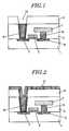
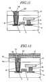
- FIG. 13illustrates a memory cell structure (cross-sectional view) of a conventional PRAM.
- An MOS transistor and a storage device with phase change materialare formed on semiconductor substrate 31 .
- Reference numeral 32denotes a gate electrode of the transistor, and diffusion layers 33 and 34 doped with n-type impurity function as source and drain regions of the transistor. Gate electrode 32 functions as a word line for memory cell selection.
- Interlayer insulating film 35is formed on the gate electrode.
- Heater electrode 38is connected to diffusion layer 33 .
- Phase change material layer 39is formed on heater electrode 38
- upper electrode 40is formed on phase change material layer 39 .
- phase change material layer 39is partially heated. This heating causes phase change in the vicinity of phase boundary between phase change material layer 39 and heater electrode 38 , and thus a change in series electrical resistance occurs. In this case, the region where the phase change occurs is illustrated as phase change region 41 in FIG. 13 .
- Ground (GND) line 37is connected via contact plug 36 to another diffusion layer 34 of the transistor.
- a storage deviceis comprised of heater electrode 38 , phase change material layer 39 and upper electrode 40 , and the storage device is connected via the MOS transistor to the GND line, whereby one memory cell is constructed.
- phase change material layer 39With GND line 37 connected to the ground and the transistor in an ON state, when a pulse voltage is applied to upper electrode 40 , electric current flows in a current path including upper electrode 40 , phase change material layer 39 , heater electrode 38 , diffusion layer 33 , transistor channel, diffusion layer 34 and GND line 37 . Such a passage of electric current causes generation of heat (Joule heat) in heater electrode 38 and thus phase change material layer 39 is partially heated, causing phase change. As a result, a change in electrical resistance value occurs.
- the phase change materialcan be set to a crystalline state (Set state) having a low resistance or a noncrystalline state (Reset state) having a high resistance. After the completion of heating, the state can be maintained. Consequently, data can be recorded (held) in a desired memory cell by using the change in electrical resistance.
- heater electrode 38is directly connected to diffusion layer 33 .
- tungsten (W) or the likecan be used; but in order to implement ohmic contact with the diffusion layer, for example, titanium (Ti) is deposited on a lowermost layer part, and subsequently titanium nitride (TiN) acting as barrier metal is deposited thereon, and then tungsten for infilling is deposited thereon.
- Tititanium
- TiNtitanium nitride
- the current densityincreases to improve the heating efficiency.
- the depth of the heater electrodeis increased, it is difficult to form a small heater electrode diameter under processing constraints. Accordingly, a large amount of current has to be provided for causing phase change. Consequently, the current ability of the transistor had to be raised.
- the size of the transistorincreases, leading to an increase in cell size. Furthermore, consumption current also increases.
- FIG. 14illustrates a memory cell structure of another conventional PRAM in which improvements have been made for the above problems.
- heater electrode 38 of FIG. 13is replaced with a stacked structure of contact plug 42 and heater electrode 46 .
- Contact plug 42is, similarly to heater electrode 38 of FIG. 13 , formed of three layers of titanium, titanium nitride and tungsten.
- Heater electrode 46is formed of tungsten or the like, and connected to an upper part of contact plug 42 .
- the height of heater electrode 46can be set lower than the structure of FIG. 13 and thus the heater diameter can be set smaller.
- the heater diameteris limited by the resolution of photolithography in patterning.
- opening 44is patterned by photolithography and thereafter side wall 45 is formed using an insulating film so that the heater diameter is reduced, the thickness of the side wall is limited by the bottom diameter of opening 44 .
- opening 44 for heater electrode and side wall 45are formed by anisotropic dry etching, in the case of microscopic contact hole, it is difficult to form a perfectly perpendicular side surface. More specifically, the side surface of opening 44 has a tapered shape, thereby becoming the bottom diameter smaller than the upper diameter. Consequently, the film thickness of side wall 45 should be reduced so that the bottom of opening 44 is not closed. Accordingly, it is difficult to reduce the upper part diameter of heater electrode 46 to a desired size.
- phase change region 41is formed in contact with a planar part on the heater electrode. Accordingly, heat and current (electron) diffuses (the arrow indicated by “H”) toward the upper electrode and thus the current density does not increase. Consequently, the heating efficiency of the heater electrode is low; in order to reach a desired temperature, a large amount of current was needed. Further, since the planar upper surface of the heater electrode is in contact with the phase change material, phase change region 41 also extends widely. Accordingly, heat amount to be added till the completion of the phase change increases to cause the phase change in a large area. This is also a factor of increasing an amount of the applied current.
- Japanese Patent Laid-Open No. 2003-332529describes a structure in which a combined electrode is formed by arranging a conductive material to cover dielectric mandrel being regular pyramid-shaped or cone-shaped insulator, and only the peak of the combined electrode is made to protrude from the dielectric layer covering the combined electrode, so that the area of contact between phase change material and heater electrode is reduced.
- this structureincludes the dielectric mandrel, and thus phase change region cannot be formed directly on a contact from a transistor formed in the lower part. As a result, the degree of integration cannot be raised, so it is difficult to reduce the chip size of device.
- phase change memory devicein which the contact area between phase change material and heater electrode can be reduced to suppress current required for heating and also the phase change region can be formed directly on the contact to raise the degree of integration.
- phase change memory deviceincluding:
- phase change material layer
- a heater electrodehaving a lower part and an upper part, and the lower part surrounded by a first insulating layer and the upper part protruding the first insulating layer and having a sharp configuration and a tip end coupled to the phase change layer.
- the upper part of the heater electrodehas a sharp configuration, and only the tip end thereof is in contact with the phase change material. Accordingly, the heating efficiency of the phase change material layer by the heater electrode improves, and thus current required for heating can be suppressed.
- the heater electrodeis connected to a source or drain region of transistor via a contact plug. Consequently, when a material having a higher resistance than a conductive material forming the contact plug is used only for the heater electrode, the heating efficiency is further improved.
- the present inventionallows suppressing of current required for heating the phase change material. Consequently, current consumption reduction and memory cell transistor size reduction (chip area reduction) can be accomplished.
- FIGS. 1 to 8are each a sectional view for describing steps in a fabrication method of a phase change memory device according to one exemplary embodiment of the present invention
- FIG. 9is a sectional view for describing the phase change memory device according to the one exemplary embodiment of the present invention.
- FIGS. 10 and 11are each a sectional view for describing steps in a fabrication method of a phase change memory device according to another exemplary embodiment of the present invention.
- FIG. 12is a sectional view for describing the phase change memory device according to another exemplary embodiment of the present invention.
- FIG. 13is a sectional view of a phase change memory device according to a first related art.
- FIG. 14is a sectional view of a phase change memory device according to a second related art.
- the second insulating material covering the sharp configuration of the heater electrodemay be formed in a configuration of side wall on the side surface of the sharp configuration on the side wall composed of the first insulating material, or formed on the whole upper surface of the side wall composed of the first insulating material.
- the phase change memory device of the present inventionmay include: a contact plug coupled between a bottom of the heater electrode and an active switching device, such as a transistor; and an upper electrode in contact with an upper surface of the phase change material layer, and the heater electrode may be constructed using a material having a greater resistance than the contact plug to raise the heating efficiency.
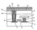
- FIG. 9is a sectional view of a PRAM memory cell according to one exemplary embodiment.
- An MOS transistor acting as an active switching deviceis formed on p-type semiconductor substrate 1 .
- Gate electrode 2 of the transistorfunctions as a word line for memory cell selection.
- Diffusion layer regions 3 and 4contain n-type impurity such as phosphorus and function as a source and drain regions of the transistor, respectively.
- Contact plug 8is connected to diffusion layer region 3 .
- Ground (GND) line 7is connected via contact plug 6 to diffusion layer region 4 .
- Heater electrode 14is arranged in contact with contact plug 8 .
- the upper part of heater electrode 14has a sharpened configuration (sharp configuration) and only the tip end thereof is in contact with phase change material layer 17 .
- Upper electrode 18is arranged in contact with phase change material layer 17 on an upper surface of phase change material layer 17 .
- Heater electrode 14has a sharpened configuration in its upper part, and the side surface thereof except for a part of the tip end thereof is covered with side wall 16 using insulating film. Consequently, only the microscopic region being a part of the sharpened tip end in the upper part of heater electrode 14 functions as a heater in contact with phase change material layer 17 . Accordingly, the current concentrates in the tip end of heater electrode 14 , so the current density increases and thus the heating efficiency improves. This allows lowering of the current value required for causing phase change. Consequently, it is possible to cause phase change using small current. Also, phase change region 19 formed in this way is smaller than the region according to related art.
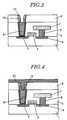
- gate electrode 2 of the MOS transistor, diffusion layer regions 3 and 4 , interlayer insulating film 5 , contact plugs 6 and 8 , and ground line 7are, using known means, formed on semiconductor substrate 1 .
- Contact plugs 6 and 8are formed of three layers of titanium, titanium nitride and tungsten stacked upwardly in this order. The surface of contact plug 8 is flattened by CMP (Chemical Mechanical Polishing).
- Interlayer insulating film 9is formed on contact plug 8 by use of silicon oxide film (SiO 2 ) or the like and thereafter opening 10 for forming the heater electrode is arranged.
- insulating film 11is formed using a first insulating material such as silicon nitride film (Si 3 N 4 )).
- the thickness of insulating film 11is set so that opening 10 is not completely filled.
- anisotropic dry etchingis subjected to insulating film 11 to form side wall 12 on a side surface of opening 10 .
- tungsten filmis deposited as heater electrode material 13 to fill a void surrounded by side wall 12 .
- heater electrode material 13is polished by CMP to expose an upper surface of side wall 12 , whereby a smooth surface is formed.
- side wall 12is partly removed by anisotropic dry etching to lower the surface of side wall 12 .
- the dry etching conditionsare set so that the speed of etching silicon nitride film forming side wall 12 is higher than the speed of etching tungsten forming heater material 13 and silicon oxide film forming interlayer insulating film 9 .
- heater material 13has a configuration in which the upper part of heater material 13 protrudes from side wall 12 .
- etching gas ionalso collides with a side surface of heater material 13 and thus removal by etching also continues in the side surface of the heater material.
- the upper side surface of heater material 13comes to have a longer time exposed to etching gas compared with the lower side surface thereof. Consequently, a tapered configuration is formed in which the diameter of the upper part is smaller than that of the lower part.
- the void surrounded by side wall 12 for filling heater material 13is very small, for example, 50 to 60 nm in diameter, so finally heater electrode 14 is formed which has a configuration with its tip end sharpened (sharp configuration).
- a second insulating materialsuch as silicon nitride is deposited approximately 10 nm to form insulating film 15 .
- heater electrode 14has a configuration with its tip end exposed alone.
- phase change material layer 17 and upper electrode 18are sequentially deposited. More specifically, as the phase change material, chalcogenide material may be used, for example.
- chalcogenide materialmeans alloy containing one or more of germanium (Ge), stibium (Sb), tellurium (Te), indium (In), selenium (Se) and the like.
- chalcogenide materialexamples include binary alloys such as GaSb, InSb, InSe Sb 2 Te 3 and GeTe, ternary alloys such as Ge 2 Sb 2 Te 5 , InSbTe, GaSeTe (GST), SnSb 2 Te 4 and InSbGe, and quaternary alloys such as AgInSbTe, (GeSn)SbTe GeSb(SeTe) and Te 81 Ge 15 Sb 2 S 2 .
- binary alloyssuch as GaSb, InSb, InSe Sb 2 Te 3 and GeTe
- ternary alloyssuch as Ge 2 Sb 2 Te 5 , InSbTe, GaSeTe (GST), SnSb 2 Te 4 and InSbGe
- quaternary alloyssuch as AgInSbTe, (GeSn)SbTe GeSb(SeTe) and Te 81 Ge 15 Sb 2 S 2 .
- titanium (Ti), titanium nitride (TiN) or laminated layer film of titanium and titanium nitridemay be used, for example.
- protective insulating filmis formed on upper electrode 18 , or an upper wiring layer is further formed, whereby the fabrication of the inventive PRAM memory cell is completed.
- the area of contact between phase change material layer 17 and heater electrode 14is reduced, so the current density increases, allowing more efficient heating of phase change material layer 17 .
- the area of contact between phase change material layer 17 and heater electrode 14decreases, the spreading width of the region (reference numeral 19 of FIG. 9 ) where phase change occurs can be suppressed.
- the phase change regionis reduced, so phase change can be accomplished using smaller heat quantity than related art. Consequently, current consumption can be significantly suppressed.
- phase changecan be made by smaller current ability of the memory cell transistor, allowing reduction in transistor size and reduction in chip area.
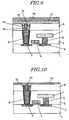
- FIGS. 10 to 12A second exemplary embodiment will be described with reference to FIGS. 10 to 12 .
- insulating film 20 of a second insulating material such as silicon nitrideis deposited 30 nm or more to completely fill the recess on side wall 12 formed in the step of FIG. 6 .
- insulating film 20is polished by dry etching or CMP to expose only the tip end-of heater electrode 14 .
- phase change material layer 17 and upper electrode 18are sequentially deposited, whereby a structure according to the second exemplary embodiment is provided.
- phase change material layer 17is in contact with heater electrode 14 only at the sharp tip end of heater electrode 14 . Consequently, the contact area is reduced compared to related art, so the current density increases, allowing more efficient heating of phase change material layer 17 by use of smaller current.
- tungstenis used for both the material forming the upper layer of contact plug 8 and the material forming the heater electrode.
- a higher-resistant materialmay be alternatively used only for the heater electrode.
- titanium nitrideTiN
- the heat generation of the heater electrodeincreases in proportion to the resistance value of heater electrode. Accordingly, when titanium nitride of a higher resistance value than tungsten is used, a desired heater temperature can be provided by a smaller current.
- a high-resistant material other than titanium nitridemay be used for both the first exemplary embodiment and the second exemplary embodiment.
- the processing for sharpening the upper part of the heater electrodeis implemented by properly setting the conditions for etching side wall 12 depending on the electrode material used.
- a structuremay be used in which n-type well is formed in the p-type semiconductor substrate and an MOS transistor is arranged in the n-type well, and impurity such as boron is used in the source and drain region to form a p-type Mos transistor.
- impuritysuch as boron
- phase change materialany material for which the resistance is varied by heating may be used; thus a material other than chalcogenide may be used.
- silicon nitride filmwas used, but the present invention is not limited thereto; for example, silicon oxide film used for the interlayer insulating film may also be used for the second insulating material.
- the present inventionrelates to a fabrication method for the phase change memory device.
- the fabrication methodis used for the phase change memory device comprising a phase change material layer and a heater electrode to heat the phase change material layer and thereby varying the resistance value of the phase change material layer to store data.
- the fabrication methodincludes:
- the second insulating materialcan be formed as film having a thickness such that the recessis not completely filled, and can be formed in a configuration of side wall on a side surface of the sharp configuration when a part of the tip end of the sharp configuration is exposed.
- the second insulating materialis formed as film to completely fill the recess and is flattened, whereby a part of the tip end of the sharp configuration is exposed.
- the process (f)is preferably for etching the interlayer insulating film, the first insulating material and the heater electrode all at once, and the etching is preferably carried out under conditions that the etching speed for the first insulating material is higher than that for the interlayer insulating film, and the etching speed for the heater electrode is higher than that for the interlayer insulating film and lower than that for the first insulating material.
- the voidis preferably smaller in width. relative to the resolution of photolithography.
- the fabrication methodcan further include forming a contact plug before the process (a), wherein in the process (b), the opening is formed so that at least a part of the upper surface of the contact plug is exposed.
- the heater electrodeis preferably made of a material having a higher resistance than the contact plug.
- the fabrication methodcan further include forming an MOS transistor, wherein the contact plug is connected to either a source or drain region of the MOS transistor.
Landscapes
- Engineering & Computer Science (AREA)
- Manufacturing & Machinery (AREA)
- Semiconductor Memories (AREA)
Abstract
Description
Claims (9)
Applications Claiming Priority (2)
| Application Number | Priority Date | Filing Date | Title |
|---|---|---|---|
| JP2008-051946 | 2008-03-03 | ||
| JP2008051946AJP2009212202A (en) | 2008-03-03 | 2008-03-03 | Phase change memory device and fabrication method thereof |
Publications (2)
| Publication Number | Publication Date |
|---|---|
| US20090218557A1 US20090218557A1 (en) | 2009-09-03 |
| US7915602B2true US7915602B2 (en) | 2011-03-29 |
Family
ID=41012478
Family Applications (1)
| Application Number | Title | Priority Date | Filing Date |
|---|---|---|---|
| US12/379,825Expired - Fee RelatedUS7915602B2 (en) | 2008-03-03 | 2009-03-03 | Phase change memory device and fabrication method thereof |
Country Status (2)
| Country | Link |
|---|---|
| US (1) | US7915602B2 (en) |
| JP (1) | JP2009212202A (en) |
Cited By (16)
| Publication number | Priority date | Publication date | Assignee | Title |
|---|---|---|---|---|
| US20120051123A1 (en)* | 2010-08-26 | 2012-03-01 | Micron Technology, Inc. | Phase change memory structures and methods |
| US20130137237A1 (en)* | 2009-09-18 | 2013-05-30 | Kabushiki Kaisha Toshiba | Semiconductor memory device and method of manufacturing the same |
| US20130285003A1 (en)* | 2012-04-30 | 2013-10-31 | Micron Technology, Inc. | Phase Change Memory Cells And Methods Of Forming Phase Change Memory Cells |
| US8975148B2 (en) | 2011-11-17 | 2015-03-10 | Micron Technology, Inc. | Memory arrays and methods of forming memory cells |
| US8994489B2 (en) | 2011-10-19 | 2015-03-31 | Micron Technology, Inc. | Fuses, and methods of forming and using fuses |
| US9118004B2 (en) | 2011-03-23 | 2015-08-25 | Micron Technology, Inc. | Memory cells and methods of forming memory cells |
| US9136467B2 (en) | 2012-04-30 | 2015-09-15 | Micron Technology, Inc. | Phase change memory cells and methods of forming phase change memory cells |
| US9252188B2 (en) | 2011-11-17 | 2016-02-02 | Micron Technology, Inc. | Methods of forming memory cells |
| US9299930B2 (en) | 2011-11-17 | 2016-03-29 | Micron Technology, Inc. | Memory cells, integrated devices, and methods of forming memory cells |
| US9343506B2 (en) | 2014-06-04 | 2016-05-17 | Micron Technology, Inc. | Memory arrays with polygonal memory cells having specific sidewall orientations |
| US9362494B2 (en) | 2014-06-02 | 2016-06-07 | Micron Technology, Inc. | Array of cross point memory cells and methods of forming an array of cross point memory cells |
| US9553262B2 (en) | 2013-02-07 | 2017-01-24 | Micron Technology, Inc. | Arrays of memory cells and methods of forming an array of memory cells |
| US9881971B2 (en) | 2014-04-01 | 2018-01-30 | Micron Technology, Inc. | Memory arrays |
| US10396125B2 (en) | 2014-11-07 | 2019-08-27 | Micron Technology, Inc. | Cross-point memory and methods for fabrication of same |
| US11038106B1 (en) | 2019-11-22 | 2021-06-15 | International Business Machines Corporation | Phase change memory cell with a metal layer |
| US11910731B2 (en) | 2021-02-10 | 2024-02-20 | International Business Machines Corporation | Embedded heater in a phase change memory material |
Families Citing this family (22)
| Publication number | Priority date | Publication date | Assignee | Title |
|---|---|---|---|---|
| US7768812B2 (en) | 2008-01-15 | 2010-08-03 | Micron Technology, Inc. | Memory cells, memory cell programming methods, memory cell reading methods, memory cell operating methods, and memory devices |
| US8211743B2 (en) | 2008-05-02 | 2012-07-03 | Micron Technology, Inc. | Methods of forming non-volatile memory cells having multi-resistive state material between conductive electrodes |
| US8134137B2 (en) | 2008-06-18 | 2012-03-13 | Micron Technology, Inc. | Memory device constructions, memory cell forming methods, and semiconductor construction forming methods |
| US9343665B2 (en) | 2008-07-02 | 2016-05-17 | Micron Technology, Inc. | Methods of forming a non-volatile resistive oxide memory cell and methods of forming a non-volatile resistive oxide memory array |
| US8470635B2 (en)* | 2009-11-30 | 2013-06-25 | Micron Technology, Inc. | Keyhole-free sloped heater for phase change memory |
| US8411477B2 (en) | 2010-04-22 | 2013-04-02 | Micron Technology, Inc. | Arrays of vertically stacked tiers of non-volatile cross point memory cells, methods of forming arrays of vertically stacked tiers of non-volatile cross point memory cells, and methods of reading a data value stored by an array of vertically stacked tiers of non-volatile cross point memory cells |
| US8427859B2 (en) | 2010-04-22 | 2013-04-23 | Micron Technology, Inc. | Arrays of vertically stacked tiers of non-volatile cross point memory cells, methods of forming arrays of vertically stacked tiers of non-volatile cross point memory cells, and methods of reading a data value stored by an array of vertically stacked tiers of non-volatile cross point memory cells |
| US8530875B1 (en)* | 2010-05-06 | 2013-09-10 | Micron Technology, Inc. | Phase change memory including ovonic threshold switch with layered electrode and methods for forming same |
| US8289763B2 (en) | 2010-06-07 | 2012-10-16 | Micron Technology, Inc. | Memory arrays |
| US8351242B2 (en) | 2010-09-29 | 2013-01-08 | Micron Technology, Inc. | Electronic devices, memory devices and memory arrays |
| US8759809B2 (en) | 2010-10-21 | 2014-06-24 | Micron Technology, Inc. | Integrated circuitry comprising nonvolatile memory cells having platelike electrode and ion conductive material layer |
| US8796661B2 (en) | 2010-11-01 | 2014-08-05 | Micron Technology, Inc. | Nonvolatile memory cells and methods of forming nonvolatile memory cell |
| US8526213B2 (en) | 2010-11-01 | 2013-09-03 | Micron Technology, Inc. | Memory cells, methods of programming memory cells, and methods of forming memory cells |
| US9454997B2 (en) | 2010-12-02 | 2016-09-27 | Micron Technology, Inc. | Array of nonvolatile memory cells having at least five memory cells per unit cell, having a plurality of the unit cells which individually comprise three elevational regions of programmable material, and/or having a continuous volume having a combination of a plurality of vertically oriented memory cells and a plurality of horizontally oriented memory cells; array of vertically stacked tiers of nonvolatile memory cells |
| US8431458B2 (en) | 2010-12-27 | 2013-04-30 | Micron Technology, Inc. | Methods of forming a nonvolatile memory cell and methods of forming an array of nonvolatile memory cells |
| US8791447B2 (en) | 2011-01-20 | 2014-07-29 | Micron Technology, Inc. | Arrays of nonvolatile memory cells and methods of forming arrays of nonvolatile memory cells |
| US8488365B2 (en) | 2011-02-24 | 2013-07-16 | Micron Technology, Inc. | Memory cells |
| US8537592B2 (en) | 2011-04-15 | 2013-09-17 | Micron Technology, Inc. | Arrays of nonvolatile memory cells and methods of forming arrays of nonvolatile memory cells |
| US9166158B2 (en) | 2013-02-25 | 2015-10-20 | Micron Technology, Inc. | Apparatuses including electrodes having a conductive barrier material and methods of forming same |
| JP2015002283A (en)* | 2013-06-17 | 2015-01-05 | ピーエスフォー ルクスコ エスエイアールエルPS4 Luxco S.a.r.l. | Semiconductor device and manufacturing method therefor |
| US10490742B2 (en) | 2017-08-28 | 2019-11-26 | Taiwan Seminconductor Manufacturing Co., Ltd. | Method for forming a phase change memory (PCM) cell with a low deviation contact area between a heater and a phase change element |
| JP6487090B1 (en)* | 2018-03-19 | 2019-03-20 | 株式会社東芝 | Nonvolatile memory device and manufacturing method thereof |
Citations (15)
| Publication number | Priority date | Publication date | Assignee | Title |
|---|---|---|---|---|
| US6147395A (en)* | 1996-10-02 | 2000-11-14 | Micron Technology, Inc. | Method for fabricating a small area of contact between electrodes |
| US6534368B2 (en)* | 1997-01-28 | 2003-03-18 | Micron Technology, Inc. | Integrated circuit memory cell having a small active area and method of forming same |
| JP2003332529A (en) | 2002-04-04 | 2003-11-21 | Hewlett Packard Co <Hp> | Multiple electrode of low heat loss and small area of contact surface for phase change medium memory device |
| US7012273B2 (en)* | 2003-08-14 | 2006-03-14 | Silicon Storage Technology, Inc. | Phase change memory device employing thermal-electrical contacts with narrowing electrical current paths |
| US7049623B2 (en)* | 2002-12-13 | 2006-05-23 | Ovonyx, Inc. | Vertical elevated pore phase change memory |
| US20060138473A1 (en) | 2004-12-24 | 2006-06-29 | Elpida Memory Inc. | Semiconductor device and manufacturing method thereof |
| US7374174B2 (en)* | 2004-12-22 | 2008-05-20 | Micron Technology, Inc. | Small electrode for resistance variable devices |
| US7394087B2 (en)* | 2004-08-17 | 2008-07-01 | Samsung Electronics Co., Ltd. | Phase-changeable memory devices and methods of forming the same |
| US7488981B2 (en)* | 2003-12-30 | 2009-02-10 | Samsung Electronics Co., Ltd. | Memory devices having sharp-tipped phase change layer patterns |
| US7498064B2 (en)* | 2004-08-02 | 2009-03-03 | Samsung Electronics Co., Ltd. | Laser reflowing of phase changeable memory element to close a void therein |
| US7554144B2 (en)* | 2006-04-17 | 2009-06-30 | Macronix International Co., Ltd. | Memory device and manufacturing method |
| US7569846B2 (en)* | 2005-05-07 | 2009-08-04 | Samsung Electronics Co., Ltd. | Phase-change memory device including nanowires and method of manufacturing the same |
| US7692176B2 (en)* | 2004-08-17 | 2010-04-06 | Samsung Electronics Co., Ltd. | Phase-changeable memory devices including an adiabatic layer |
| US7704787B2 (en)* | 2003-02-24 | 2010-04-27 | Samsung Electronics Co., Ltd. | Methods for fabricating phase changeable memory devices |
| US7835177B2 (en)* | 2005-12-21 | 2010-11-16 | Industrial Technology Research Institute | Phase change memory cell and method of fabricating |
Family Cites Families (2)
| Publication number | Priority date | Publication date | Assignee | Title |
|---|---|---|---|---|
| DE102005025209B4 (en)* | 2004-05-27 | 2011-01-13 | Samsung Electronics Co., Ltd., Suwon | Semiconductor memory device, electronic system and method for manufacturing a semiconductor memory device |
| KR20070028604A (en)* | 2004-06-30 | 2007-03-12 | 코닌클리즈케 필립스 일렉트로닉스 엔.브이. | Electrical apparatus having a layer of conductive material contacted by nanowires and manufacturing method thereof |
- 2008
- 2008-03-03JPJP2008051946Apatent/JP2009212202A/ennot_activeCeased
- 2009
- 2009-03-03USUS12/379,825patent/US7915602B2/ennot_activeExpired - Fee Related
Patent Citations (17)
| Publication number | Priority date | Publication date | Assignee | Title |
|---|---|---|---|---|
| US6147395A (en)* | 1996-10-02 | 2000-11-14 | Micron Technology, Inc. | Method for fabricating a small area of contact between electrodes |
| US6534368B2 (en)* | 1997-01-28 | 2003-03-18 | Micron Technology, Inc. | Integrated circuit memory cell having a small active area and method of forming same |
| JP2003332529A (en) | 2002-04-04 | 2003-11-21 | Hewlett Packard Co <Hp> | Multiple electrode of low heat loss and small area of contact surface for phase change medium memory device |
| US6670628B2 (en) | 2002-04-04 | 2003-12-30 | Hewlett-Packard Company, L.P. | Low heat loss and small contact area composite electrode for a phase change media memory device |
| US7049623B2 (en)* | 2002-12-13 | 2006-05-23 | Ovonyx, Inc. | Vertical elevated pore phase change memory |
| US7704787B2 (en)* | 2003-02-24 | 2010-04-27 | Samsung Electronics Co., Ltd. | Methods for fabricating phase changeable memory devices |
| US7012273B2 (en)* | 2003-08-14 | 2006-03-14 | Silicon Storage Technology, Inc. | Phase change memory device employing thermal-electrical contacts with narrowing electrical current paths |
| US7488981B2 (en)* | 2003-12-30 | 2009-02-10 | Samsung Electronics Co., Ltd. | Memory devices having sharp-tipped phase change layer patterns |
| US7498064B2 (en)* | 2004-08-02 | 2009-03-03 | Samsung Electronics Co., Ltd. | Laser reflowing of phase changeable memory element to close a void therein |
| US7692176B2 (en)* | 2004-08-17 | 2010-04-06 | Samsung Electronics Co., Ltd. | Phase-changeable memory devices including an adiabatic layer |
| US7394087B2 (en)* | 2004-08-17 | 2008-07-01 | Samsung Electronics Co., Ltd. | Phase-changeable memory devices and methods of forming the same |
| US7374174B2 (en)* | 2004-12-22 | 2008-05-20 | Micron Technology, Inc. | Small electrode for resistance variable devices |
| JP2006179778A (en) | 2004-12-24 | 2006-07-06 | Elpida Memory Inc | Semiconductor device and its manufacturing method |
| US20060138473A1 (en) | 2004-12-24 | 2006-06-29 | Elpida Memory Inc. | Semiconductor device and manufacturing method thereof |
| US7569846B2 (en)* | 2005-05-07 | 2009-08-04 | Samsung Electronics Co., Ltd. | Phase-change memory device including nanowires and method of manufacturing the same |
| US7835177B2 (en)* | 2005-12-21 | 2010-11-16 | Industrial Technology Research Institute | Phase change memory cell and method of fabricating |
| US7554144B2 (en)* | 2006-04-17 | 2009-06-30 | Macronix International Co., Ltd. | Memory device and manufacturing method |
Cited By (34)
| Publication number | Priority date | Publication date | Assignee | Title |
|---|---|---|---|---|
| US20130137237A1 (en)* | 2009-09-18 | 2013-05-30 | Kabushiki Kaisha Toshiba | Semiconductor memory device and method of manufacturing the same |
| US8835241B2 (en)* | 2009-09-18 | 2014-09-16 | Kabushiki Kaisha Toshiba | Method of manufacturing a semiconductor memory device |
| US8243506B2 (en)* | 2010-08-26 | 2012-08-14 | Micron Technology, Inc. | Phase change memory structures and methods |
| US8493772B2 (en) | 2010-08-26 | 2013-07-23 | Micron Technology, Inc. | Phase change memory structures and methods |
| US20120051123A1 (en)* | 2010-08-26 | 2012-03-01 | Micron Technology, Inc. | Phase change memory structures and methods |
| US9118004B2 (en) | 2011-03-23 | 2015-08-25 | Micron Technology, Inc. | Memory cells and methods of forming memory cells |
| US9236566B2 (en) | 2011-03-23 | 2016-01-12 | Micron Technology, Inc. | Memory cells and methods of forming memory cells |
| US11222762B2 (en) | 2011-10-19 | 2022-01-11 | Micron Technology, Inc. | Fuses, and methods of forming and using fuses |
| US10290456B2 (en) | 2011-10-19 | 2019-05-14 | Micron Technology, Inc. | Methods of forming and using fuses |
| US9514905B2 (en) | 2011-10-19 | 2016-12-06 | Micron Technology, Inc. | Fuses, and methods of forming and using fuses |
| US8994489B2 (en) | 2011-10-19 | 2015-03-31 | Micron Technology, Inc. | Fuses, and methods of forming and using fuses |
| US9893277B2 (en) | 2011-11-17 | 2018-02-13 | Micron Technology, Inc. | Memory arrays and methods of forming memory cells |
| US8975148B2 (en) | 2011-11-17 | 2015-03-10 | Micron Technology, Inc. | Memory arrays and methods of forming memory cells |
| US10069067B2 (en) | 2011-11-17 | 2018-09-04 | Micron Technology, Inc. | Memory arrays and methods of forming memory cells |
| US9252188B2 (en) | 2011-11-17 | 2016-02-02 | Micron Technology, Inc. | Methods of forming memory cells |
| US9299930B2 (en) | 2011-11-17 | 2016-03-29 | Micron Technology, Inc. | Memory cells, integrated devices, and methods of forming memory cells |
| US9570677B2 (en) | 2011-11-17 | 2017-02-14 | Micron Technology, Inc. | Memory cells, integrated devices, and methods of forming memory cells |
| US8765555B2 (en)* | 2012-04-30 | 2014-07-01 | Micron Technology, Inc. | Phase change memory cells and methods of forming phase change memory cells |
| US9076963B2 (en)* | 2012-04-30 | 2015-07-07 | Micron Technology, Inc. | Phase change memory cells and methods of forming phase change memory cells |
| US20130285003A1 (en)* | 2012-04-30 | 2013-10-31 | Micron Technology, Inc. | Phase Change Memory Cells And Methods Of Forming Phase Change Memory Cells |
| US9136467B2 (en) | 2012-04-30 | 2015-09-15 | Micron Technology, Inc. | Phase change memory cells and methods of forming phase change memory cells |
| US20140252302A1 (en)* | 2012-04-30 | 2014-09-11 | Micron Technology, Inc. | Phase Change Memory Cells And Methods Of Forming Phase Change Memory Cells |
| US9773977B2 (en) | 2012-04-30 | 2017-09-26 | Micron Technology, Inc. | Phase change memory cells |
| US9553262B2 (en) | 2013-02-07 | 2017-01-24 | Micron Technology, Inc. | Arrays of memory cells and methods of forming an array of memory cells |
| US9881971B2 (en) | 2014-04-01 | 2018-01-30 | Micron Technology, Inc. | Memory arrays |
| US10332934B2 (en) | 2014-04-01 | 2019-06-25 | Micron Technology, Inc. | Memory arrays and methods of forming memory arrays |
| US9362494B2 (en) | 2014-06-02 | 2016-06-07 | Micron Technology, Inc. | Array of cross point memory cells and methods of forming an array of cross point memory cells |
| US9673393B2 (en) | 2014-06-04 | 2017-06-06 | Micron Technology, Inc. | Methods of forming memory arrays |
| US9917253B2 (en) | 2014-06-04 | 2018-03-13 | Micron Technology, Inc. | Methods of forming memory arrays |
| US9343506B2 (en) | 2014-06-04 | 2016-05-17 | Micron Technology, Inc. | Memory arrays with polygonal memory cells having specific sidewall orientations |
| US10396125B2 (en) | 2014-11-07 | 2019-08-27 | Micron Technology, Inc. | Cross-point memory and methods for fabrication of same |
| US10680037B2 (en) | 2014-11-07 | 2020-06-09 | Micron Technology, Inc. | Cross-point memory and methods for fabrication of same |
| US11038106B1 (en) | 2019-11-22 | 2021-06-15 | International Business Machines Corporation | Phase change memory cell with a metal layer |
| US11910731B2 (en) | 2021-02-10 | 2024-02-20 | International Business Machines Corporation | Embedded heater in a phase change memory material |
Also Published As
| Publication number | Publication date |
|---|---|
| JP2009212202A (en) | 2009-09-17 |
| US20090218557A1 (en) | 2009-09-03 |
Similar Documents
| Publication | Publication Date | Title |
|---|---|---|
| US7915602B2 (en) | Phase change memory device and fabrication method thereof | |
| US8901009B2 (en) | Methods of manufacturing semiconductor devices | |
| US7067837B2 (en) | Phase-change memory devices | |
| US8426967B2 (en) | Scaled-down phase change memory cell in recessed heater | |
| US7728319B2 (en) | Vertical phase change memory cell and methods for manufacturing thereof | |
| US7838860B2 (en) | Integrated circuit including vertical diode | |
| US20070063180A1 (en) | Electrically rewritable non-volatile memory element and method of manufacturing the same | |
| US7868312B2 (en) | Semiconductor memory device and manufacturing method thereof | |
| US9219231B2 (en) | Phase change memory cells with surfactant layers | |
| CN1787224A (en) | Manufacturing method of memory element, memory element and phase-change memory element | |
| US8648326B2 (en) | Phase change memory electrode with sheath for reduced programming current | |
| CN101877384B (en) | Low Operating Current Phase Change Memory Element Structure | |
| US7545019B2 (en) | Integrated circuit including logic portion and memory portion | |
| US20110089394A1 (en) | Semiconductor device | |
| USRE45580E1 (en) | Phase-change nonvolatile memory and manufacturing method therefor | |
| KR20130012385A (en) | Semiconductor device and method for manufacturing the same | |
| US20140301137A1 (en) | Phase-change memory device having phase-change region divided into multi layers and operating method thereof | |
| TWI726023B (en) | Memory device | |
| US20090108248A1 (en) | Integrated circuit including doped semiconductor line having conductive cladding | |
| US8853660B2 (en) | Semiconductor memory devices having lower and upper interconnections, selection components and memory components | |
| US8254166B2 (en) | Integrated circuit including doped semiconductor line having conductive cladding | |
| JP2011216768A (en) | Semiconductor device, and method of manufacturing the same | |
| KR101078718B1 (en) | Phase change RAM device and method of manufacturing the same |
Legal Events
| Date | Code | Title | Description |
|---|---|---|---|
| AS | Assignment | Owner name:ELPIDA MEMORY, INC., JAPAN Free format text:ASSIGNMENT OF ASSIGNORS INTEREST;ASSIGNOR:SATO, NATSUKI;REEL/FRAME:022388/0689 Effective date:20090225 | |
| FEPP | Fee payment procedure | Free format text:PAYOR NUMBER ASSIGNED (ORIGINAL EVENT CODE: ASPN); ENTITY STATUS OF PATENT OWNER: LARGE ENTITY | |
| STCF | Information on status: patent grant | Free format text:PATENTED CASE | |
| AS | Assignment | Owner name:ELPIDA MEMORY INC., JAPAN Free format text:SECURITY AGREEMENT;ASSIGNOR:PS4 LUXCO S.A.R.L.;REEL/FRAME:032414/0261 Effective date:20130726 | |
| AS | Assignment | Owner name:PS4 LUXCO S.A.R.L., LUXEMBOURG Free format text:ASSIGNMENT OF ASSIGNORS INTEREST;ASSIGNOR:ELPIDA MEMORY, INC.;REEL/FRAME:032896/0727 Effective date:20130726 | |
| FPAY | Fee payment | Year of fee payment:4 | |
| FEPP | Fee payment procedure | Free format text:PAYER NUMBER DE-ASSIGNED (ORIGINAL EVENT CODE: RMPN); ENTITY STATUS OF PATENT OWNER: LARGE ENTITY Free format text:PAYOR NUMBER ASSIGNED (ORIGINAL EVENT CODE: ASPN); ENTITY STATUS OF PATENT OWNER: LARGE ENTITY | |
| AS | Assignment | Owner name:PS5 LUXCO S.A.R.L., LUXEMBOURG Free format text:ASSIGNMENT OF ASSIGNORS INTEREST;ASSIGNOR:PS4 LUXCO S.A.R.L.;REEL/FRAME:039818/0506 Effective date:20130829 Owner name:LONGITUDE SEMICONDUCTOR S.A.R.L., LUXEMBOURG Free format text:CHANGE OF NAME;ASSIGNOR:PS5 LUXCO S.A.R.L.;REEL/FRAME:039793/0880 Effective date:20131112 | |
| AS | Assignment | Owner name:LONGITUDE LICENSING LIMITED, IRELAND Free format text:ASSIGNMENT OF ASSIGNORS INTEREST;ASSIGNOR:LONGITUDE SEMICONDUCTOR S.A.R.L.;REEL/FRAME:046865/0667 Effective date:20180731 | |
| FEPP | Fee payment procedure | Free format text:MAINTENANCE FEE REMINDER MAILED (ORIGINAL EVENT CODE: REM.); ENTITY STATUS OF PATENT OWNER: LARGE ENTITY | |
| LAPS | Lapse for failure to pay maintenance fees | Free format text:PATENT EXPIRED FOR FAILURE TO PAY MAINTENANCE FEES (ORIGINAL EVENT CODE: EXP.); ENTITY STATUS OF PATENT OWNER: LARGE ENTITY | |
| STCH | Information on status: patent discontinuation | Free format text:PATENT EXPIRED DUE TO NONPAYMENT OF MAINTENANCE FEES UNDER 37 CFR 1.362 | |
| FP | Lapsed due to failure to pay maintenance fee | Effective date:20190329 |