US7911044B2 - RF module package for releasing stress - Google Patents
RF module package for releasing stressDownload PDFInfo
- Publication number
- US7911044B2 US7911044B2US11/647,448US64744806AUS7911044B2US 7911044 B2US7911044 B2US 7911044B2US 64744806 AUS64744806 AUS 64744806AUS 7911044 B2US7911044 B2US 7911044B2
- Authority
- US
- United States
- Prior art keywords
- substrate
- dice
- die
- rdl
- package
- Prior art date
- Legal status (The legal status is an assumption and is not a legal conclusion. Google has not performed a legal analysis and makes no representation as to the accuracy of the status listed.)
- Active, expires
Links
- 239000000758substrateSubstances0.000claimsabstractdescription74
- 229910001020Au alloyInorganic materials0.000claimsabstractdescription7
- 238000009826distributionMethods0.000claimsabstractdescription5
- 229910000881Cu alloyInorganic materials0.000claimsabstractdescription4
- 229910000990Ni alloyInorganic materials0.000claimsabstractdescription4
- 229910045601alloyInorganic materials0.000claimsabstractdescription3
- 239000000956alloySubstances0.000claimsabstractdescription3
- 239000002184metalSubstances0.000claimsdescription38
- 229910052751metalInorganic materials0.000claimsdescription38
- 239000000463materialSubstances0.000claimsdescription30
- 238000000034methodMethods0.000claimsdescription24
- 239000011521glassSubstances0.000claimsdescription8
- JBRZTFJDHDCESZ-UHFFFAOYSA-NAsGaChemical compound[As]#[Ga]JBRZTFJDHDCESZ-UHFFFAOYSA-N0.000claimsdescription7
- 239000004593EpoxySubstances0.000claimsdescription7
- XUIMIQQOPSSXEZ-UHFFFAOYSA-NSiliconChemical compound[Si]XUIMIQQOPSSXEZ-UHFFFAOYSA-N0.000claimsdescription7
- 239000000919ceramicSubstances0.000claimsdescription5
- 238000001816coolingMethods0.000claimsdescription5
- 239000010703siliconSubstances0.000claimsdescription5
- 229910052710siliconInorganic materials0.000claimsdescription5
- 239000010949copperSubstances0.000description22
- 229910000679solderInorganic materials0.000description10
- 239000011248coating agentSubstances0.000description8
- 238000000576coating methodMethods0.000description8
- 230000035882stressEffects0.000description8
- 230000001351cycling effectEffects0.000description7
- 238000009713electroplatingMethods0.000description7
- 230000017525heat dissipationEffects0.000description7
- 238000004544sputter depositionMethods0.000description5
- 239000003989dielectric materialSubstances0.000description4
- 238000005516engineering processMethods0.000description4
- 238000004519manufacturing processMethods0.000description4
- 239000004065semiconductorSubstances0.000description4
- 238000012360testing methodMethods0.000description4
- 238000001039wet etchingMethods0.000description4
- 239000003990capacitorSubstances0.000description3
- 239000013013elastic materialSubstances0.000description3
- 239000011888foilSubstances0.000description3
- 239000003292glueSubstances0.000description3
- 229920002379silicone rubberPolymers0.000description3
- 239000004945silicone rubberSubstances0.000description3
- 230000008646thermal stressEffects0.000description3
- 239000004642PolyimideSubstances0.000description2
- 230000015572biosynthetic processEffects0.000description2
- 229910052802copperInorganic materials0.000description2
- 238000011161developmentMethods0.000description2
- 230000009477glass transitionEffects0.000description2
- 238000013007heat curingMethods0.000description2
- 238000004806packaging method and processMethods0.000description2
- 229920001721polyimidePolymers0.000description2
- 229920001296polysiloxanePolymers0.000description2
- 239000002904solventSubstances0.000description2
- 229910021654trace metalInorganic materials0.000description2
- JYEUMXHLPRZUAT-UHFFFAOYSA-N1,2,3-triazineChemical compoundC1=CN=NN=C1JYEUMXHLPRZUAT-UHFFFAOYSA-N0.000description1
- XQUPVDVFXZDTLT-UHFFFAOYSA-N1-[4-[[4-(2,5-dioxopyrrol-1-yl)phenyl]methyl]phenyl]pyrrole-2,5-dioneChemical compoundO=C1C=CC(=O)N1C(C=C1)=CC=C1CC1=CC=C(N2C(C=CC2=O)=O)C=C1XQUPVDVFXZDTLT-UHFFFAOYSA-N0.000description1
- 241001133184Colletotrichum agavesSpecies0.000description1
- RYGMFSIKBFXOCR-UHFFFAOYSA-NCopperChemical compound[Cu]RYGMFSIKBFXOCR-UHFFFAOYSA-N0.000description1
- 229910001069Ti alloyInorganic materials0.000description1
- 238000003848UV Light-CuringMethods0.000description1
- 238000004458analytical methodMethods0.000description1
- 238000004140cleaningMethods0.000description1
- 238000004891communicationMethods0.000description1
- 239000002131composite materialSubstances0.000description1
- 150000001875compoundsChemical class0.000description1
- KPUWHANPEXNPJT-UHFFFAOYSA-NdisiloxaneChemical class[SiH3]O[SiH3]KPUWHANPEXNPJT-UHFFFAOYSA-N0.000description1
- 229920001971elastomerPolymers0.000description1
- 238000005530etchingMethods0.000description1
- 238000013100final testMethods0.000description1
- 229910052737goldInorganic materials0.000description1
- 238000001459lithographyMethods0.000description1
- 239000000203mixtureSubstances0.000description1
- 238000012986modificationMethods0.000description1
- 230000004048modificationEffects0.000description1
- 238000012858packaging processMethods0.000description1
- 239000004033plasticSubstances0.000description1
- 238000007747platingMethods0.000description1
- 229920003192poly(bis maleimide)Polymers0.000description1
- 229920000642polymerPolymers0.000description1
- 238000007639printingMethods0.000description1
- 238000012545processingMethods0.000description1
- 230000005855radiationEffects0.000description1
- 229920005989resinPolymers0.000description1
- 239000011347resinSubstances0.000description1
- 229920002050silicone resinPolymers0.000description1
Images


Classifications
- H—ELECTRICITY
- H01—ELECTRIC ELEMENTS
- H01L—SEMICONDUCTOR DEVICES NOT COVERED BY CLASS H10
- H01L23/00—Details of semiconductor or other solid state devices
- H01L23/12—Mountings, e.g. non-detachable insulating substrates
- H—ELECTRICITY
- H01—ELECTRIC ELEMENTS
- H01L—SEMICONDUCTOR DEVICES NOT COVERED BY CLASS H10
- H01L23/00—Details of semiconductor or other solid state devices
- H01L23/52—Arrangements for conducting electric current within the device in operation from one component to another, i.e. interconnections, e.g. wires, lead frames
- H01L23/538—Arrangements for conducting electric current within the device in operation from one component to another, i.e. interconnections, e.g. wires, lead frames the interconnection structure between a plurality of semiconductor chips being formed on, or in, insulating substrates
- H01L23/5389—Arrangements for conducting electric current within the device in operation from one component to another, i.e. interconnections, e.g. wires, lead frames the interconnection structure between a plurality of semiconductor chips being formed on, or in, insulating substrates the chips being integrally enclosed by the interconnect and support structures
- H—ELECTRICITY
- H01—ELECTRIC ELEMENTS
- H01L—SEMICONDUCTOR DEVICES NOT COVERED BY CLASS H10
- H01L23/00—Details of semiconductor or other solid state devices
- H01L23/34—Arrangements for cooling, heating, ventilating or temperature compensation ; Temperature sensing arrangements
- H01L23/46—Arrangements for cooling, heating, ventilating or temperature compensation ; Temperature sensing arrangements involving the transfer of heat by flowing fluids
- H01L23/467—Arrangements for cooling, heating, ventilating or temperature compensation ; Temperature sensing arrangements involving the transfer of heat by flowing fluids by flowing gases, e.g. air
- H—ELECTRICITY
- H01—ELECTRIC ELEMENTS
- H01L—SEMICONDUCTOR DEVICES NOT COVERED BY CLASS H10
- H01L23/00—Details of semiconductor or other solid state devices
- H01L23/58—Structural electrical arrangements for semiconductor devices not otherwise provided for, e.g. in combination with batteries
- H01L23/64—Impedance arrangements
- H01L23/66—High-frequency adaptations
- H—ELECTRICITY
- H01—ELECTRIC ELEMENTS
- H01L—SEMICONDUCTOR DEVICES NOT COVERED BY CLASS H10
- H01L24/00—Arrangements for connecting or disconnecting semiconductor or solid-state bodies; Methods or apparatus related thereto
- H01L24/01—Means for bonding being attached to, or being formed on, the surface to be connected, e.g. chip-to-package, die-attach, "first-level" interconnects; Manufacturing methods related thereto
- H01L24/18—High density interconnect [HDI] connectors; Manufacturing methods related thereto
- H01L24/23—Structure, shape, material or disposition of the high density interconnect connectors after the connecting process
- H01L24/24—Structure, shape, material or disposition of the high density interconnect connectors after the connecting process of an individual high density interconnect connector
- H—ELECTRICITY
- H01—ELECTRIC ELEMENTS
- H01L—SEMICONDUCTOR DEVICES NOT COVERED BY CLASS H10
- H01L24/00—Arrangements for connecting or disconnecting semiconductor or solid-state bodies; Methods or apparatus related thereto
- H01L24/80—Methods for connecting semiconductor or other solid state bodies using means for bonding being attached to, or being formed on, the surface to be connected
- H01L24/82—Methods for connecting semiconductor or other solid state bodies using means for bonding being attached to, or being formed on, the surface to be connected by forming build-up interconnects at chip-level, e.g. for high density interconnects [HDI]
- H—ELECTRICITY
- H01—ELECTRIC ELEMENTS
- H01L—SEMICONDUCTOR DEVICES NOT COVERED BY CLASS H10
- H01L25/00—Assemblies consisting of a plurality of semiconductor or other solid state devices
- H01L25/16—Assemblies consisting of a plurality of semiconductor or other solid state devices the devices being of types provided for in two or more different subclasses of H10B, H10D, H10F, H10H, H10K or H10N, e.g. forming hybrid circuits
- H—ELECTRICITY
- H01—ELECTRIC ELEMENTS
- H01L—SEMICONDUCTOR DEVICES NOT COVERED BY CLASS H10
- H01L2224/00—Indexing scheme for arrangements for connecting or disconnecting semiconductor or solid-state bodies and methods related thereto as covered by H01L24/00
- H01L2224/01—Means for bonding being attached to, or being formed on, the surface to be connected, e.g. chip-to-package, die-attach, "first-level" interconnects; Manufacturing methods related thereto
- H01L2224/18—High density interconnect [HDI] connectors; Manufacturing methods related thereto
- H01L2224/23—Structure, shape, material or disposition of the high density interconnect connectors after the connecting process
- H01L2224/24—Structure, shape, material or disposition of the high density interconnect connectors after the connecting process of an individual high density interconnect connector
- H01L2224/241—Disposition
- H01L2224/24135—Connecting between different semiconductor or solid-state bodies, i.e. chip-to-chip
- H01L2224/24137—Connecting between different semiconductor or solid-state bodies, i.e. chip-to-chip the bodies being arranged next to each other, e.g. on a common substrate
- H—ELECTRICITY
- H01—ELECTRIC ELEMENTS
- H01L—SEMICONDUCTOR DEVICES NOT COVERED BY CLASS H10
- H01L2224/00—Indexing scheme for arrangements for connecting or disconnecting semiconductor or solid-state bodies and methods related thereto as covered by H01L24/00
- H01L2224/01—Means for bonding being attached to, or being formed on, the surface to be connected, e.g. chip-to-package, die-attach, "first-level" interconnects; Manufacturing methods related thereto
- H01L2224/26—Layer connectors, e.g. plate connectors, solder or adhesive layers; Manufacturing methods related thereto
- H01L2224/31—Structure, shape, material or disposition of the layer connectors after the connecting process
- H01L2224/32—Structure, shape, material or disposition of the layer connectors after the connecting process of an individual layer connector
- H01L2224/321—Disposition
- H01L2224/32151—Disposition the layer connector connecting between a semiconductor or solid-state body and an item not being a semiconductor or solid-state body, e.g. chip-to-substrate, chip-to-passive
- H01L2224/32221—Disposition the layer connector connecting between a semiconductor or solid-state body and an item not being a semiconductor or solid-state body, e.g. chip-to-substrate, chip-to-passive the body and the item being stacked
- H01L2224/32245—Disposition the layer connector connecting between a semiconductor or solid-state body and an item not being a semiconductor or solid-state body, e.g. chip-to-substrate, chip-to-passive the body and the item being stacked the item being metallic
- H—ELECTRICITY
- H01—ELECTRIC ELEMENTS
- H01L—SEMICONDUCTOR DEVICES NOT COVERED BY CLASS H10
- H01L2224/00—Indexing scheme for arrangements for connecting or disconnecting semiconductor or solid-state bodies and methods related thereto as covered by H01L24/00
- H01L2224/73—Means for bonding being of different types provided for in two or more of groups H01L2224/10, H01L2224/18, H01L2224/26, H01L2224/34, H01L2224/42, H01L2224/50, H01L2224/63, H01L2224/71
- H01L2224/732—Location after the connecting process
- H01L2224/73251—Location after the connecting process on different surfaces
- H01L2224/73267—Layer and HDI connectors
- H—ELECTRICITY
- H01—ELECTRIC ELEMENTS
- H01L—SEMICONDUCTOR DEVICES NOT COVERED BY CLASS H10
- H01L2924/00—Indexing scheme for arrangements or methods for connecting or disconnecting semiconductor or solid-state bodies as covered by H01L24/00
- H01L2924/01—Chemical elements
- H01L2924/01005—Boron [B]
- H—ELECTRICITY
- H01—ELECTRIC ELEMENTS
- H01L—SEMICONDUCTOR DEVICES NOT COVERED BY CLASS H10
- H01L2924/00—Indexing scheme for arrangements or methods for connecting or disconnecting semiconductor or solid-state bodies as covered by H01L24/00
- H01L2924/01—Chemical elements
- H01L2924/01006—Carbon [C]
- H—ELECTRICITY
- H01—ELECTRIC ELEMENTS
- H01L—SEMICONDUCTOR DEVICES NOT COVERED BY CLASS H10
- H01L2924/00—Indexing scheme for arrangements or methods for connecting or disconnecting semiconductor or solid-state bodies as covered by H01L24/00
- H01L2924/01—Chemical elements
- H01L2924/01015—Phosphorus [P]
- H—ELECTRICITY
- H01—ELECTRIC ELEMENTS
- H01L—SEMICONDUCTOR DEVICES NOT COVERED BY CLASS H10
- H01L2924/00—Indexing scheme for arrangements or methods for connecting or disconnecting semiconductor or solid-state bodies as covered by H01L24/00
- H01L2924/01—Chemical elements
- H01L2924/01019—Potassium [K]
- H—ELECTRICITY
- H01—ELECTRIC ELEMENTS
- H01L—SEMICONDUCTOR DEVICES NOT COVERED BY CLASS H10
- H01L2924/00—Indexing scheme for arrangements or methods for connecting or disconnecting semiconductor or solid-state bodies as covered by H01L24/00
- H01L2924/01—Chemical elements
- H01L2924/01027—Cobalt [Co]
- H—ELECTRICITY
- H01—ELECTRIC ELEMENTS
- H01L—SEMICONDUCTOR DEVICES NOT COVERED BY CLASS H10
- H01L2924/00—Indexing scheme for arrangements or methods for connecting or disconnecting semiconductor or solid-state bodies as covered by H01L24/00
- H01L2924/01—Chemical elements
- H01L2924/01029—Copper [Cu]
- H—ELECTRICITY
- H01—ELECTRIC ELEMENTS
- H01L—SEMICONDUCTOR DEVICES NOT COVERED BY CLASS H10
- H01L2924/00—Indexing scheme for arrangements or methods for connecting or disconnecting semiconductor or solid-state bodies as covered by H01L24/00
- H01L2924/01—Chemical elements
- H01L2924/01033—Arsenic [As]
- H—ELECTRICITY
- H01—ELECTRIC ELEMENTS
- H01L—SEMICONDUCTOR DEVICES NOT COVERED BY CLASS H10
- H01L2924/00—Indexing scheme for arrangements or methods for connecting or disconnecting semiconductor or solid-state bodies as covered by H01L24/00
- H01L2924/01—Chemical elements
- H01L2924/01047—Silver [Ag]
- H—ELECTRICITY
- H01—ELECTRIC ELEMENTS
- H01L—SEMICONDUCTOR DEVICES NOT COVERED BY CLASS H10
- H01L2924/00—Indexing scheme for arrangements or methods for connecting or disconnecting semiconductor or solid-state bodies as covered by H01L24/00
- H01L2924/01—Chemical elements
- H01L2924/01059—Praseodymium [Pr]
- H—ELECTRICITY
- H01—ELECTRIC ELEMENTS
- H01L—SEMICONDUCTOR DEVICES NOT COVERED BY CLASS H10
- H01L2924/00—Indexing scheme for arrangements or methods for connecting or disconnecting semiconductor or solid-state bodies as covered by H01L24/00
- H01L2924/01—Chemical elements
- H01L2924/01068—Erbium [Er]
- H—ELECTRICITY
- H01—ELECTRIC ELEMENTS
- H01L—SEMICONDUCTOR DEVICES NOT COVERED BY CLASS H10
- H01L2924/00—Indexing scheme for arrangements or methods for connecting or disconnecting semiconductor or solid-state bodies as covered by H01L24/00
- H01L2924/01—Chemical elements
- H01L2924/01074—Tungsten [W]
- H—ELECTRICITY
- H01—ELECTRIC ELEMENTS
- H01L—SEMICONDUCTOR DEVICES NOT COVERED BY CLASS H10
- H01L2924/00—Indexing scheme for arrangements or methods for connecting or disconnecting semiconductor or solid-state bodies as covered by H01L24/00
- H01L2924/01—Chemical elements
- H01L2924/01075—Rhenium [Re]
- H—ELECTRICITY
- H01—ELECTRIC ELEMENTS
- H01L—SEMICONDUCTOR DEVICES NOT COVERED BY CLASS H10
- H01L2924/00—Indexing scheme for arrangements or methods for connecting or disconnecting semiconductor or solid-state bodies as covered by H01L24/00
- H01L2924/01—Chemical elements
- H01L2924/01078—Platinum [Pt]
- H—ELECTRICITY
- H01—ELECTRIC ELEMENTS
- H01L—SEMICONDUCTOR DEVICES NOT COVERED BY CLASS H10
- H01L2924/00—Indexing scheme for arrangements or methods for connecting or disconnecting semiconductor or solid-state bodies as covered by H01L24/00
- H01L2924/01—Chemical elements
- H01L2924/01079—Gold [Au]
- H—ELECTRICITY
- H01—ELECTRIC ELEMENTS
- H01L—SEMICONDUCTOR DEVICES NOT COVERED BY CLASS H10
- H01L2924/00—Indexing scheme for arrangements or methods for connecting or disconnecting semiconductor or solid-state bodies as covered by H01L24/00
- H01L2924/01—Chemical elements
- H01L2924/01082—Lead [Pb]
- H—ELECTRICITY
- H01—ELECTRIC ELEMENTS
- H01L—SEMICONDUCTOR DEVICES NOT COVERED BY CLASS H10
- H01L2924/00—Indexing scheme for arrangements or methods for connecting or disconnecting semiconductor or solid-state bodies as covered by H01L24/00
- H01L2924/01—Chemical elements
- H01L2924/01087—Francium [Fr]
- H—ELECTRICITY
- H01—ELECTRIC ELEMENTS
- H01L—SEMICONDUCTOR DEVICES NOT COVERED BY CLASS H10
- H01L2924/00—Indexing scheme for arrangements or methods for connecting or disconnecting semiconductor or solid-state bodies as covered by H01L24/00
- H01L2924/013—Alloys
- H01L2924/014—Solder alloys
- H—ELECTRICITY
- H01—ELECTRIC ELEMENTS
- H01L—SEMICONDUCTOR DEVICES NOT COVERED BY CLASS H10
- H01L2924/00—Indexing scheme for arrangements or methods for connecting or disconnecting semiconductor or solid-state bodies as covered by H01L24/00
- H01L2924/095—Indexing scheme for arrangements or methods for connecting or disconnecting semiconductor or solid-state bodies as covered by H01L24/00 with a principal constituent of the material being a combination of two or more materials provided in the groups H01L2924/013 - H01L2924/0715
- H01L2924/097—Glass-ceramics, e.g. devitrified glass
- H01L2924/09701—Low temperature co-fired ceramic [LTCC]
- H—ELECTRICITY
- H01—ELECTRIC ELEMENTS
- H01L—SEMICONDUCTOR DEVICES NOT COVERED BY CLASS H10
- H01L2924/00—Indexing scheme for arrangements or methods for connecting or disconnecting semiconductor or solid-state bodies as covered by H01L24/00
- H01L2924/10—Details of semiconductor or other solid state devices to be connected
- H01L2924/102—Material of the semiconductor or solid state bodies
- H01L2924/1025—Semiconducting materials
- H01L2924/10251—Elemental semiconductors, i.e. Group IV
- H01L2924/10253—Silicon [Si]
- H—ELECTRICITY
- H01—ELECTRIC ELEMENTS
- H01L—SEMICONDUCTOR DEVICES NOT COVERED BY CLASS H10
- H01L2924/00—Indexing scheme for arrangements or methods for connecting or disconnecting semiconductor or solid-state bodies as covered by H01L24/00
- H01L2924/10—Details of semiconductor or other solid state devices to be connected
- H01L2924/102—Material of the semiconductor or solid state bodies
- H01L2924/1025—Semiconducting materials
- H01L2924/1026—Compound semiconductors
- H01L2924/1032—III-V
- H01L2924/10329—Gallium arsenide [GaAs]
- H—ELECTRICITY
- H01—ELECTRIC ELEMENTS
- H01L—SEMICONDUCTOR DEVICES NOT COVERED BY CLASS H10
- H01L2924/00—Indexing scheme for arrangements or methods for connecting or disconnecting semiconductor or solid-state bodies as covered by H01L24/00
- H01L2924/10—Details of semiconductor or other solid state devices to be connected
- H01L2924/11—Device type
- H01L2924/14—Integrated circuits
- H—ELECTRICITY
- H01—ELECTRIC ELEMENTS
- H01L—SEMICONDUCTOR DEVICES NOT COVERED BY CLASS H10
- H01L2924/00—Indexing scheme for arrangements or methods for connecting or disconnecting semiconductor or solid-state bodies as covered by H01L24/00
- H01L2924/15—Details of package parts other than the semiconductor or other solid state devices to be connected
- H01L2924/151—Die mounting substrate
- H01L2924/153—Connection portion
- H01L2924/1531—Connection portion the connection portion being formed only on the surface of the substrate opposite to the die mounting surface
- H01L2924/15311—Connection portion the connection portion being formed only on the surface of the substrate opposite to the die mounting surface being a ball array, e.g. BGA
- H—ELECTRICITY
- H01—ELECTRIC ELEMENTS
- H01L—SEMICONDUCTOR DEVICES NOT COVERED BY CLASS H10
- H01L2924/00—Indexing scheme for arrangements or methods for connecting or disconnecting semiconductor or solid-state bodies as covered by H01L24/00
- H01L2924/19—Details of hybrid assemblies other than the semiconductor or other solid state devices to be connected
- H01L2924/1901—Structure
- H01L2924/19011—Structure including integrated passive components
- H—ELECTRICITY
- H01—ELECTRIC ELEMENTS
- H01L—SEMICONDUCTOR DEVICES NOT COVERED BY CLASS H10
- H01L2924/00—Indexing scheme for arrangements or methods for connecting or disconnecting semiconductor or solid-state bodies as covered by H01L24/00
- H01L2924/19—Details of hybrid assemblies other than the semiconductor or other solid state devices to be connected
- H01L2924/1901—Structure
- H01L2924/1904—Component type
- H01L2924/19041—Component type being a capacitor
- H—ELECTRICITY
- H01—ELECTRIC ELEMENTS
- H01L—SEMICONDUCTOR DEVICES NOT COVERED BY CLASS H10
- H01L2924/00—Indexing scheme for arrangements or methods for connecting or disconnecting semiconductor or solid-state bodies as covered by H01L24/00
- H01L2924/19—Details of hybrid assemblies other than the semiconductor or other solid state devices to be connected
- H01L2924/1901—Structure
- H01L2924/1904—Component type
- H01L2924/19042—Component type being an inductor
- H—ELECTRICITY
- H01—ELECTRIC ELEMENTS
- H01L—SEMICONDUCTOR DEVICES NOT COVERED BY CLASS H10
- H01L2924/00—Indexing scheme for arrangements or methods for connecting or disconnecting semiconductor or solid-state bodies as covered by H01L24/00
- H01L2924/19—Details of hybrid assemblies other than the semiconductor or other solid state devices to be connected
- H01L2924/1901—Structure
- H01L2924/1904—Component type
- H01L2924/19043—Component type being a resistor
- H—ELECTRICITY
- H01—ELECTRIC ELEMENTS
- H01L—SEMICONDUCTOR DEVICES NOT COVERED BY CLASS H10
- H01L2924/00—Indexing scheme for arrangements or methods for connecting or disconnecting semiconductor or solid-state bodies as covered by H01L24/00
- H01L2924/30—Technical effects
- H01L2924/301—Electrical effects
- H01L2924/30105—Capacitance
- H—ELECTRICITY
- H01—ELECTRIC ELEMENTS
- H01L—SEMICONDUCTOR DEVICES NOT COVERED BY CLASS H10
- H01L2924/00—Indexing scheme for arrangements or methods for connecting or disconnecting semiconductor or solid-state bodies as covered by H01L24/00
- H01L2924/30—Technical effects
- H01L2924/301—Electrical effects
- H01L2924/3025—Electromagnetic shielding
- H—ELECTRICITY
- H01—ELECTRIC ELEMENTS
- H01L—SEMICONDUCTOR DEVICES NOT COVERED BY CLASS H10
- H01L2924/00—Indexing scheme for arrangements or methods for connecting or disconnecting semiconductor or solid-state bodies as covered by H01L24/00
- H01L2924/30—Technical effects
- H01L2924/35—Mechanical effects
- H01L2924/351—Thermal stress
Definitions
- This inventionrelates to a structure of package, and more particularly to a RF (radio frequency) module package with die receiving through-hole of substrate to improve the reliability and to reduce the device size.
- RFradio frequency
- the device densityis increased and the device dimension is reduced, continuously.
- the demand for the packaging or interconnecting techniques in such high density devicesis also increased to fit the situation mentioned above.
- an array of solder bumpsis formed on the surface of the die.
- the formation of the solder bumpsmay be carried out by using a solder composite material through a solder mask for producing a desired pattern of solder bumps.
- the function of chip packageincludes power distribution, signal distribution, heat dissipation, protection and support . . . and so on.
- the traditional package techniquefor example lead frame package, flex package, rigid package technique, can't meet the demand of producing smaller chip with high density elements on the chip.
- Wafer level packageis to be understood as meaning that the entire packaging and all the interconnections on the wafer as well as other processing steps are carried out before the singulation (dicing) into chips (dies).
- singulationsingulation
- the MCMmay also contain passive components, e.g. capacitors, inductors, and resistors.
- a typical arrangement for RF packageis an RF circuit chip and a capacitor mounted on the substrate.
- the substratecan be laminate, ceramic, silicon, or other appropriate material. It is because the rapid development of communication technology, the RF package is more important than ever.
- the requirements for the RF moduleincludes high circuit density, low electrical loss, excellent dimensional control, high heat dissipation, robust substrate, higher reliability on board and lower cost.
- the prior RF module packageemploys LTCC (low-temperature co-fired ceramic) and the disadvantage is listed as follows; Low On Board Reliability (TCT—temperature cycling test); Need extra metal plate for heat dissipation, Long manufacturing cycle; Higher manufacturing cost; IC need to be packaged in advance; Still need wire bonding or SMT (surface mount technology) process; Thick package body ( ⁇ 1.4 mm).
- TCTtemperature cycling test
- SMTsurface mount technology
- the present inventionprovides a RF module package to fit the requirement above.
- the object of the present inventionis to provide RF module package with excellent thermal dissipation, CTE performance and shrinkage size.
- An RF module packagecomprising: a substrate with a die receiving through holes and contact conductive pads and metal through holes; a conductive slice (foil) attached on a lower surface of said substrate; multiple dice disposed within said die receiving through hole and on said conductive slice; multiple dielectric stacking structure stacked on said multiple dice and said substrate; multiple re-distribution layers (RDL) formed (includes the inductors and resistors) within said multiple dielectric stacking structure and coupled to said dice; a top conductive layer formed over said multiple dielectric stacking structure. And heat sink materials (includes the Molecular cooling fans) are formed on said top conductive layer. Conductive bumps maybe coupled to said pluralities of terminal pads.
- FIG. 1illustrates a cross-sectional view of a structure of RF module package according to the present invention. (LGA type)
- FIG. 2illustrates a cross-sectional view of a structure of RF module package according to the present invention. (BGA type)
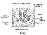
- FIG. 3illustrates a top view of a structure of RF module package according to the present invention.
- FIG. 4illustrates a top view of the RF module package according to the present invention.
- FIG. 5illustrates a top view of the RF module package according to the present invention.
- FIG. 6illustrates a bottom view of the RF module package according to the present invention.
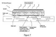
- FIG. 7illustrates a cross-sectional view of a structure of RF module package on board according to the present invention.
- the present inventiondiscloses a structure of RF module package utilizing a substrate having predetermined terminal contact metal pads 3 and metal through holes 15 formed thereon and a pre-formed die receiving through holes 4 formed into the substrate 2 .
- a multi-dice 6are (chip a, chip b and chip n) disposed within the die receiving through hole of the substrate, an elastic core paste material is filled into the space between dice, die edge and side wall of die receiving through hole of the substrate.
- a photosensitive materialis coated over the die and the pre-formed substrate (includes the core paste area).
- the material of the photosensitive materialis formed of elastic material.
- FIG. 1illustrates a cross-sectional view of RF module package in accordance with one embodiment of the present invention.
- the structureincludes a substrate 2 having a terminal contact metal pads 3 and metal through holes 15 (for organic substrate) and die receiving through holes 4 formed therein to receive multiple dice 6 .
- the multiple dice 6are including the silicon chips and gallium arsenic chips (GaAs)
- the through holes 4are formed from the upper surface of the substrate through the substrate to the lower surface.
- the through hole 4is pre-formed within the substrate 2 .
- a conductive slice (foil) 21is attached on the lower surface of the substrate 2 , preferably, the conductive slice 21 is formed by plating Cu or laminated Cu.
- the dice 6are disposed within the die receiving through holes 4 on the substrate 2 .
- contact pads (Bonding pads) 10are formed on the dice 6 .
- a first photosensitive layer or dielectric layer 12is formed over the multiple dice 6 and the upper surface of substrate and core paste 13 is filled within the space between the dice 6 , die edge and the sidewalls of the through holes 4 .
- Pluralities of openingsare formed within the dielectric layer 12 through the lithography process or exposure and develop procedure. The pluralities of openings are aligned to the contact pads or I/O pads 10 and terminal contact metal pads 3 on the substrate, respectively.
- the first RDL (redistribution layer) 14is formed on the first dielectric layer 12 by removing selected portions of metal layer formed over the layer 12 , wherein the first RDL 14 keep electrically connection with the dice 6 through the I/O pads 10 and terminal contact metal pads 3 . A part of the material of the first RDL will re-fills into the openings in the first dielectric layer 12 .
- the pads 3is coupled to the pads 18 (lower side of substrate) through the metal through hole 15 in the substrate 2 .
- a second dielectric layer 12 a with second RDL 14 a and a third dielectric layer 12 b with top metal layer 16are subsequently formed over the first dielectric layer 12 , thereby constructing a stacked interconnection structure with multi-layers RDL.
- the second RDL 14 acouples the dice through first RDL 14
- the top metal layer 16may couple to either first RDL 14 or second RDL 14 a.
- the layer 16is a conductive (metal or alloy) layer 16 that covers the third dielectric layer 12 b .
- a heat sink 17is formed atop the metal layer 16 for better thermal dissipation.
- the heat sink 17is mode of molecular cooling fan.
- the molecular groupsvibrate with more energy at higher surface temperature. The vibration can relax after emitting a phone, infrared radiation, allowing the substrate to release energy even when the surroundings are also warm.
- Terminal pads 18are located under the substrate 2 and connected to the first RDL 14 , 14 a , 16 and contact metal pads 3 of the substrate.
- the dielectric layer 12is formed atop of the multiple dice 6 and substrate 2 and refilling material such as elastic core paste. They act as buffer to absorb the thermal mechanical stress between the dice 6 and substrate 2 during temperature cycling due to the dielectric layer 12 is elastic property.
- the aforementioned structureconstructs LGA type package.
- the pads 3may be formed within the dielectric layer 12 , over the substrate 2 and maybe aligned to the terminal pad 18 .
- An alternative embodimentcan be seen in FIG. 2 , conductive balls 20 are formed on the terminal pads 18 . This type is called BGA type.
- the other partsare similar to FIG. 1 , therefore, the detailed description is omitted.
- the terminal pads 18act as the UBM (under ball metal) under the BGA scheme in the case.
- the material of the substrate 2is organic substrate likes epoxy type FR5, BT, PCB with defined through holes or Cu metal with pre etching circuit.
- the CTEis the same as the one of the mother board (PCB).
- the organic substrate with high Glass transition temperature (Tg)are epoxy type FR5 or BT (Bismaleimide triazine) type substrate.
- the Cu metal (CTE around 16)can be used also.
- the glass, ceramic, siliconcan be used as the substrate.
- the elastic core pasteis formed of silicone rubber elastic materials, it maybe the same with the die attached materials.
- the CTE (X/Y direction) of the epoxy type organic substrate (FR5/BT)is around 16 and the CTE of the tool for chip redistribution is around 5 to 8 by employing the glass materials as the tool.
- the FR5/BTis unlikely to return to original location after the temperature cycling (the temperature is close to Glass transition temperature Tg) that causes the die shift in panel form during the WLP process which needs several high temperature process.
- TgGlass transition temperature
- FIG. 3is the top view of RF module package.
- the packageincludes power amplifier, band pass filter, switch, low noise amplifier, integrated passive device (IPD) formed on the substrate.
- IPDintegrated passive device
- FIG. 4illustrates further embodiment of the present invention.
- a text, character, logomay be marked on the top metal layer 16 as shown in FIG. 5 .
- the top layercan be a ground shielding, heat sink.
- FIG. 6is the bottom view of the present invention.
- the dielectric layer 12 , 12 a , 12 bare preferably an elastic dielectric material which is made by silicone dielectric based materials comprising siloxane polymers (SINR), Dow Corning WL5000 series, and the combination thereof.
- the dielectric layeris made by a material comprising, polyimides (PI) or silicone resin.
- PIpolyimides
- the elastic dielectric layeris a kind of material with CTE larger than 100 (ppm/° C.), elongation rate about 40 percent (preferably 30 percent-50 percent), and the hardness of the material is between plastic and rubber.
- the thickness of the elastic dielectric layer 18depends on the stress accumulated in the RDL/dielectric layer interface during temperature cycling test.
- FIG. 7it illustrates the major portions that associate with the CTE issue.
- the silicon dice(CTE is ⁇ 2.3) is packaged inside the package.
- FR5 or BT organic epoxy type material(CTE ⁇ 16) is employed as the substrate and its CTE is the same as the PCB or Mother Board.
- the space (gap) between the dice and the substrateis filled with filling material (prefer the elastic core paste) to absorb the thermal mechanical stress due to CTE mismatching (between die and the epoxy type FR5/BT).
- the dielectric layers 12include elastic materials to absorb the stress between the die pads and the PCB.
- the RDL metalis Cu/Au materials and the CTE is around 16 that is the same as the PCB and organic substrate, and the UBM 18 of contact bump be located on the terminal contact metal pads 3 of substrate.
- the metal land of PCBis Cu composition metal, the CTE of Cu is around 16 that is match to the one of PCB. From the description above, the present invention may provide excellent CTE (fully matching in X/Y direction) solution for the WLP.
- CTE matching issue under the build up layers (PCB and substrate)is solved by the present scheme and it provides better reliability (no thermal stress in X/Y directions for terminal pads (solder balls/bumps) on the substrate during on board level condition) and the elastic DL is employed to absorb the Z direction stress.
- the space (gap) between chip edge and sidewall of through holes of substratecan be used to fill the elastic dielectric materials to absorb the mechanical/thermal stress.
- the material of the RDLs 14 , and 14 acomprise Ti/Cu/Au alloy or Ti/Cu/Ni/Au alloy; the thickness of the RDL 14 is between 2 um_and — 15 um.
- the Ti/Cu alloyis formed by sputtering technique also as seed metal layers, and the Cu/Au or Cu/Ni/Au alloy is formed by electroplating; exploiting the electro-plating process to form the RDL can make the RDL thick enough and better mechanical properties to withstand CTE mismatching during temperature cycling. If the structure of FO-WLP utilizes SINR as the elastic dielectric layer and Cu as the RDL, according the stress analysis not shown here, the stress accumulated in the RDL/dielectric layer interface is reduced.
- the structure and function of RDLs 14are used as the build in inductors and resistors, preferably, the inductors are located on the top of capacitors of IPD (integrated passive device), it can generates the best electrical performance to reduce the electrical loss; it is due to the low dielectric constant and control of thickness, space, line width of RDLs 14 ; preferably the metal thickness between 4 um to 10 um, metal space around 10 um and metal width around 12 um to get better electrical performance.
- the function of combine the conductive slice 21 (lower side of substrate) and top conductive layer 16are used for better thermal management and ground shielding; preferably, to use the sputtering the seed metal on the back-side of chips and electro-plating the Cu/Ni/Au to reach the thickness around 15 um to 25 um (the back side of chips are ground (GND) due to the chips (GaAs) with ground via holes on the back side), the conductive slice 21 may be solder join with ground pads of PCB to get the better heat dissipation and grounding.
- the top conductive layer 16is connecting to ground signal (GND); preferably, the material of conductive layer is Cu for better heat conductivity and ground shielding, it may be coated the heat sink materials to enhance the thermal management (preferably the molecular cooling fan to handle the heat dissipation).
- GNDground signal
- the material of conductive layeris Cu for better heat conductivity and ground shielding, it may be coated the heat sink materials to enhance the thermal management (preferably the molecular cooling fan to handle the heat dissipation).
- the RDLs 14fans out of the die and communicates toward the terminal pads.
- the dice 6is received within the pre-formed die receiving through hole of the substrate, thereby reducing the thickness of the package.
- the prior artviolates the rule to reduce the die package thickness.
- the package of the present inventionwill be thinner than the prior art.
- the substrateis pre-prepared before package.
- the through hole 4is pre-determined. Thus, the throughput will be improved than ever.
- the present inventiondiscloses a fan-out WLP with reduced thickness and good CTE matching performance.
- the present inventionincludes preparing a dicing sawed wafer in blue tape form (GaAs) and preparing the die redistribution tool (Glass base) with patterned glues and alignment pattern on the tool, followed by employing a pick and place with fine alignment system to pick and place the selected chips on the tool and patterned glues stick the die active surface.
- the substrateis bonding on the tool and patterned glues stick the substrate.
- a Vacuum printingis performed to print the core paste material (silicone rubber) into the gap between the die edge and the side wall of die through holes of substrate.
- the core pasteis cured and special solvent is used to release the panel wafer and tool. Thereafter, the panel wafer is cleaned.
- the seed metalis sputtered on the back side of the panel.
- PRis coating and forming the desired pattern. Electro-plating is performed to form the Cu/Ni/Au ( ⁇ 25 um).
- the PRis stripped and wet etching is used to form the ground metal Pads and terminal pads.
- the Glass Carrieris bounded on the back side of panel and UV curing is used to attached the Glass carrier and the Panel.
- the steps to form the RDLincludes:
- the Glass carrieris removed by special solvent and/or UV light; the panel is typing on the blue tape in flame type.
- the panel final testingis performed by using the flame type probing system.
- the panelsubstrate-FR5/BT is cut to separate the package unit.
- Elastic core paste(resin, epoxy compound, silicone rubber, etc.) is refilled the space between the dice edge and the sidewall of the through holes for thermal stress releasing buffer in the present invention, then, vacuum heat curing is applied.
- CTE mismatching issueis overcome during panel form process (using the glass carrier with lower CTE that close to silicon die) and the deepness between die and substrate FR5/BT is same level, the surface level of die (active surface side) and substrate can be the same after the die and substrate are attached on the glass carrier, and separated the panel wafer from the die redistribution tool. For example, as shown in FIGS. 1 and 2 , the top surface of the core paste 13 , the die 6 and the substrate 2 are at the same plane.
- silicone dielectric materialpreferably SINR
- substratepreferably FR45 or BT
- the contact padsare opened by using photo mask process only due to the dielectric layer (SINR) is photosensitive layer for opening the contacting open.
- the conductive slice (foil) materialis plated on the back-side of dice and substrate be solder join together with PCB.
- the reliability for both package and board levelis better than ever, especially, for the board level temperature cycling test, it was due to the CTE of substrate and PCB mother board are identical, hence, no thermal mechanical stress be applied on the solder bumps/balls; the previous failure mode (solder ball crack) during temperature cycling on board test were not obvious.
- the costis low and the process is simple. It is easy to form the multi-chips package too.
Landscapes
- Engineering & Computer Science (AREA)
- Microelectronics & Electronic Packaging (AREA)
- Computer Hardware Design (AREA)
- Power Engineering (AREA)
- Physics & Mathematics (AREA)
- Condensed Matter Physics & Semiconductors (AREA)
- General Physics & Mathematics (AREA)
- Cooling Or The Like Of Semiconductors Or Solid State Devices (AREA)
- Combinations Of Printed Boards (AREA)
Abstract
Description
- Cleaning the upper side of panel by wet/dry clean;
- Coating the dielectric layer 1 and open the bonding pads and metal contact pads on substrate (panel);
- Sputtering the Ti/Cu as seed metal layers;
- PR coating and to form the RDL pattern;
- Electro-plating Cu/Au (4 um˜10 um), and then stripping the PR and wet etching to form the first RDL trace metal;
- Coating the dielectric layer 2 and open the contact Vias;
- Sputtering the Ti/Cu as seed metal layer;
- PR coating and forming the RDL pattern (including the inductors);
- Electro-plating Cu/Au (4 um˜10 um), then removing PR and wet etching to form the second RDL trace metal;
- Coating the dielectric layer 3 (thick than 50 um) and opening the ground contact Vias;
- Sputtering the seed metal layers (Ti/Cu);
- PR coating and forming the top ground metal pattern;
- Electro-plating Cu/Au (˜15 um), PR strip and wet etching to form the ground pads on top (including the character of top mark);
- Coating the heat sink materials—molecular cooling fan on the top metal (<10 um) to enhance the heat dissipation.
- Low Cost: materials and process;
- Better performance on board Reliability (TCT);
- The CTE of Substrate FR5 matches to the one of PCB FR4 (˜16);
- Better Thermal Management—employing metal to handle heat dissipation; Copper thermal conductive k=380, LTCC k=3-5
- Using GaAs for IPD due to Low Electrical Loss, high Q;
- Dielectric materials: low k (<3), Dielectric constant for Ceramic k=3-5;
Claims (8)
Priority Applications (8)
| Application Number | Priority Date | Filing Date | Title |
|---|---|---|---|
| US11/647,448US7911044B2 (en) | 2006-12-29 | 2006-12-29 | RF module package for releasing stress |
| US11/980,498US20080157340A1 (en) | 2006-12-29 | 2007-10-31 | RF module package |
| TW096143922ATWI413231B (en) | 2006-12-29 | 2007-11-20 | Rf module package |
| SG200719012-7ASG144119A1 (en) | 2006-12-29 | 2007-12-26 | Rf module package |
| DE102007063301ADE102007063301A1 (en) | 2006-12-29 | 2007-12-27 | Radio frequency module package structure has substrate with die receiving perforations, conducting contacting connections and metallic perforations, where conducting disk is fixed under surface of substrate |
| JP2007340288AJP2008166821A (en) | 2006-12-29 | 2007-12-28 | RF module package and method for forming the same |
| KR1020070139925AKR20080063182A (en) | 2006-12-29 | 2007-12-28 | RF Module Package |
| CN200710300833XACN101211903B (en) | 2006-12-29 | 2007-12-29 | Encapsulation structure of radio frequency module and its forming method |
Applications Claiming Priority (1)
| Application Number | Priority Date | Filing Date | Title |
|---|---|---|---|
| US11/647,448US7911044B2 (en) | 2006-12-29 | 2006-12-29 | RF module package for releasing stress |
Related Child Applications (1)
| Application Number | Title | Priority Date | Filing Date |
|---|---|---|---|
| US11/980,498Continuation-In-PartUS20080157340A1 (en) | 2006-12-29 | 2007-10-31 | RF module package |
Publications (2)
| Publication Number | Publication Date |
|---|---|
| US20080157341A1 US20080157341A1 (en) | 2008-07-03 |
| US7911044B2true US7911044B2 (en) | 2011-03-22 |
Family
ID=39466024
Family Applications (1)
| Application Number | Title | Priority Date | Filing Date |
|---|---|---|---|
| US11/647,448Active2027-02-12US7911044B2 (en) | 2006-12-29 | 2006-12-29 | RF module package for releasing stress |
Country Status (6)
| Country | Link |
|---|---|
| US (1) | US7911044B2 (en) |
| JP (1) | JP2008166821A (en) |
| KR (1) | KR20080063182A (en) |
| CN (1) | CN101211903B (en) |
| DE (1) | DE102007063301A1 (en) |
| SG (1) | SG144119A1 (en) |
Cited By (11)
| Publication number | Priority date | Publication date | Assignee | Title |
|---|---|---|---|---|
| US20110042824A1 (en)* | 2009-08-20 | 2011-02-24 | Fujitsu Limited | Multi-chip module and method of manufacturing the same |
| US20120286408A1 (en)* | 2011-05-10 | 2012-11-15 | Conexant Systems, Inc. | Wafer level package with thermal pad for higher power dissipation |
| US20150311182A1 (en)* | 2014-04-24 | 2015-10-29 | SK Hynix Inc. | Semiconductor package and method for manufacturing the same |
| US9607966B2 (en) | 2012-03-27 | 2017-03-28 | Infineon Technologies Ag | Chip arrangement |
| US9793140B2 (en) | 2013-12-30 | 2017-10-17 | Taiwan Semiconductor Manufacturing Company, Ltd. | Staggered via redistribution layer (RDL) for a package and a method for forming the same |
| US20180012869A1 (en)* | 2011-03-31 | 2018-01-11 | Sony Semiconductor Solutions Corporation | Methods of forming bonded semiconductor structures, and semiconductor structures formed by such methods |
| US10177103B1 (en) | 2017-07-04 | 2019-01-08 | Samsung Electro-Mechanics Co., Ltd. | Fan-out semiconductor package |
| US11088079B2 (en)* | 2019-06-27 | 2021-08-10 | Taiwan Semiconductor Manufacturing Co., Ltd. | Package structure having line connected via portions |
| US11217874B2 (en) | 2019-04-15 | 2022-01-04 | Analog Devices, Inc. | Silicon cavity backed radiator structure |
| US12009274B2 (en) | 2021-02-16 | 2024-06-11 | Samsung Electronics Co., Ltd. | Semiconductor package including thermal exhaust pathway |
| US12021047B2 (en) | 2018-03-23 | 2024-06-25 | Taiwan Semiconductor Manufacturing Company, Ltd. | Semiconductor packages having a die, an encapsulant, and a redistribution structure |
Families Citing this family (57)
| Publication number | Priority date | Publication date | Assignee | Title |
|---|---|---|---|---|
| US7791191B2 (en)* | 2006-12-28 | 2010-09-07 | Sandisk Corporation | Semiconductor device having multiple die redistribution layer |
| US7560304B2 (en)* | 2006-12-28 | 2009-07-14 | Sandisk Corporation | Method of making a semiconductor device having multiple die redistribution layer |
| US7812434B2 (en)* | 2007-01-03 | 2010-10-12 | Advanced Chip Engineering Technology Inc | Wafer level package with die receiving through-hole and method of the same |
| US20080157398A1 (en)* | 2007-01-03 | 2008-07-03 | Advanced Chip Engineering Technology Inc. | Semiconductor device package having pseudo chips |
| KR100826989B1 (en)* | 2007-06-20 | 2008-05-02 | 주식회사 하이닉스반도체 | Semiconductor package and manufacturing method thereof |
| US8063469B2 (en)* | 2008-09-30 | 2011-11-22 | Infineon Technologies Ag | On-chip radio frequency shield with interconnect metallization |
| US7948064B2 (en) | 2008-09-30 | 2011-05-24 | Infineon Technologies Ag | System on a chip with on-chip RF shield |
| US8169059B2 (en)* | 2008-09-30 | 2012-05-01 | Infineon Technologies Ag | On-chip RF shields with through substrate conductors |
| US8889548B2 (en) | 2008-09-30 | 2014-11-18 | Infineon Technologies Ag | On-chip RF shields with backside redistribution lines |
| US8178953B2 (en)* | 2008-09-30 | 2012-05-15 | Infineon Technologies Ag | On-chip RF shields with front side redistribution lines |
| FR2937796A1 (en)* | 2008-10-29 | 2010-04-30 | St Microelectronics Grenoble | SEMICONDUCTOR DEVICE WITH PROTECTION SCREEN |
| JP5372579B2 (en)* | 2009-04-10 | 2013-12-18 | 新光電気工業株式会社 | Semiconductor device, manufacturing method thereof, and electronic device |
| CN101866892B (en)* | 2009-04-20 | 2011-12-07 | 财团法人工业技术研究院 | Chip layout structure and method |
| CN102054787B (en)* | 2010-10-21 | 2013-08-14 | 日月光半导体制造股份有限公司 | Stacked packaging structure and manufacturing method thereof |
| US8338294B2 (en) | 2011-03-31 | 2012-12-25 | Soitec | Methods of forming bonded semiconductor structures including two or more processed semiconductor structures carried by a common substrate, and semiconductor structures formed by such methods |
| CN102361028A (en)* | 2011-10-11 | 2012-02-22 | 日月光半导体制造股份有限公司 | Semiconductor package structure with multi-bump structure |
| CN103107103A (en)* | 2011-11-11 | 2013-05-15 | 北京大学深圳研究生院 | Reconfigurable operator array structure scale extension method based on wafer level packaging (WLP) form |
| CN103151316B (en)* | 2011-12-06 | 2017-10-20 | 北京大学深圳研究生院 | A kind of Expansion method of the reconfigurable operator array structure based on MCP package form |
| US9111949B2 (en) | 2012-04-09 | 2015-08-18 | Taiwan Semiconductor Manufacturing Company, Ltd. | Methods and apparatus of wafer level package for heterogeneous integration technology |
| US10373930B2 (en)* | 2012-08-10 | 2019-08-06 | Cyntec Co., Ltd | Package structure and the method to fabricate thereof |
| US8816500B2 (en)* | 2012-12-14 | 2014-08-26 | Infineon Technologies Ag | Semiconductor device having peripheral polymer structures |
| US9741655B2 (en)* | 2013-01-15 | 2017-08-22 | Silergy Semiconductor Technology (Hangzhou) Ltd | Integrated circuit common-mode filters with ESD protection and manufacturing method |
| KR101430349B1 (en)* | 2013-03-06 | 2014-08-13 | 인파크 테크놀러지 컴퍼니 리미티드 | Multifunction semiconductor package structure and method of manufacturing the same |
| CN105027278A (en)* | 2013-03-07 | 2015-11-04 | 住友电木株式会社 | Apparatus, composition for adhesive, and adhesive sheet |
| US8928117B1 (en)* | 2013-08-01 | 2015-01-06 | Taiwan Semiconductor Manufacturing Company, Ltd. | Multi-chip package structure and method of forming same |
| US8927412B1 (en)* | 2013-08-01 | 2015-01-06 | Taiwan Semiconductor Manufacturing Company, Ltd. | Multi-chip package and method of formation |
| CN104952839B (en)* | 2014-03-28 | 2018-05-04 | 恒劲科技股份有限公司 | Packaging device and manufacturing method thereof |
| CN105280574B (en)* | 2014-07-16 | 2018-12-04 | 日月光半导体制造股份有限公司 | Element embedded type packaging structure and manufacturing method thereof |
| TWI543323B (en)* | 2014-08-12 | 2016-07-21 | 矽品精密工業股份有限公司 | Interposer and method of manufacture |
| CN104241219B (en) | 2014-08-26 | 2019-06-21 | 日月光半导体制造股份有限公司 | Element embedded packaging structure and manufacturing method thereof |
| US9589927B2 (en)* | 2014-09-19 | 2017-03-07 | Nxp Usa, Inc. | Packaged RF amplifier devices with grounded isolation structures and methods of manufacture thereof |
| JP2016149743A (en) | 2015-02-15 | 2016-08-18 | スカイワークス ソリューションズ, インコーポレイテッドSkyworks Solutions, Inc. | Power amplifier reduced in size through elimination of matching network |
| US9893684B2 (en) | 2015-02-15 | 2018-02-13 | Skyworks Solutions, Inc. | Radio-frequency power amplifiers driven by boost converter |
| US9472484B2 (en)* | 2015-02-17 | 2016-10-18 | Avago Technologies General Ip (Singapore) Pte. Ltd. | Semiconductor structure having thermal backside core |
| CN105187014A (en)* | 2015-06-29 | 2015-12-23 | 苏州英诺迅科技股份有限公司 | GaAs and LDMOS/GaN hybrid integrated microwave power amplifier based on BT substrate |
| CN105428250B (en)* | 2015-11-25 | 2017-12-26 | 中国电子科技集团公司第二十九研究所 | A kind of method of ltcc substrate surface cavity planarization process |
| US9842820B1 (en)* | 2015-12-04 | 2017-12-12 | Altera Corporation | Wafer-level fan-out wirebond packages |
| WO2017111956A1 (en)* | 2015-12-22 | 2017-06-29 | Intel Corporation | Semiconductor package with electromagnetic interference shielding |
| US9904776B2 (en) | 2016-02-10 | 2018-02-27 | Taiwan Semiconductor Manufacturing Company, Ltd. | Fingerprint sensor pixel array and methods of forming same |
| US20180166356A1 (en)* | 2016-12-13 | 2018-06-14 | Globalfoundries Inc. | Fan-out circuit packaging with integrated lid |
| KR102009905B1 (en)* | 2017-02-21 | 2019-08-12 | 삼성전자주식회사 | Fan-out semiconductor package |
| TWI626724B (en)* | 2017-04-07 | 2018-06-11 | 思鷺科技股份有限公司 | Package structure |
| US10157864B1 (en) | 2017-07-27 | 2018-12-18 | Taiwan Semiconductor Manufacturing Co., Ltd. | Package structure and method of forming the same |
| DE112017007887T5 (en)* | 2017-09-29 | 2020-05-07 | Intel Corporation | ANTENNA PACKAGE WITH BALL MOUNT ARRAY TO CONNECT ANTENNA AND BASE SUBSTRATES |
| US10861814B2 (en)* | 2017-11-02 | 2020-12-08 | Taiwan Semiconductor Manufacturing Company, Ltd. | Integrated fan-out packages and methods of forming the same |
| CN108269791B (en)* | 2018-02-06 | 2023-12-08 | 深圳市傲科光电子有限公司 | Hybrid printed circuit board |
| TWI667871B (en)* | 2018-08-07 | 2019-08-01 | 國立交通大學 | Fan device |
| US20200243484A1 (en)* | 2019-01-30 | 2020-07-30 | Avago Technologies International Sales Pte. Limited | Radio frequency (rf) switch device including rf switch integrated circuit (ic) divided between sides of pcb |
| US10985101B2 (en)* | 2019-03-14 | 2021-04-20 | Taiwan Semiconductor Manufacturing Company, Ltd. | Semiconductor package and manufacturing method thereof |
| US11164804B2 (en)* | 2019-07-23 | 2021-11-02 | International Business Machines Corporation | Integrated circuit (IC) device package lid attach utilizing nano particle metallic paste |
| US11011448B2 (en) | 2019-08-01 | 2021-05-18 | Intel Corporation | IC package including multi-chip unit with bonded integrated heat spreader |
| US11503704B2 (en)* | 2019-12-30 | 2022-11-15 | General Electric Company | Systems and methods for hybrid glass and organic packaging for radio frequency electronics |
| CN113517200B (en) | 2020-05-27 | 2024-06-07 | 台湾积体电路制造股份有限公司 | Semiconductor device and method for forming the same |
| KR20220033636A (en)* | 2020-09-09 | 2022-03-17 | 삼성전자주식회사 | Semiconductor package |
| WO2022222015A1 (en)* | 2021-04-20 | 2022-10-27 | Huawei Technologies Co., Ltd. | Semiconductor package |
| US20230065844A1 (en)* | 2021-08-30 | 2023-03-02 | Taiwan Semiconductor Manufacturing Company, Ltd. | Semiconductor package and method of manufacturing the same |
| KR20230140244A (en) | 2022-03-29 | 2023-10-06 | 삼성전자주식회사 | Semiconductor package |
Citations (11)
| Publication number | Priority date | Publication date | Assignee | Title |
|---|---|---|---|---|
| US20020070443A1 (en)* | 2000-12-08 | 2002-06-13 | Xiao-Chun Mu | Microelectronic package having an integrated heat sink and build-up layers |
| US20050062147A1 (en)* | 2003-09-19 | 2005-03-24 | Casio Computer Co., Ltd. | Semiconductor device having heat dissipation layer |
| US20050121770A1 (en)* | 2003-12-05 | 2005-06-09 | Baek Seung D. | Wafer-level electronic modules with integral connector contacts and methods of fabricating the same |
| US20050212107A1 (en)* | 2004-03-29 | 2005-09-29 | Atsushi Kato | Circuit device and manufacturing method thereof |
| US20060087037A1 (en)* | 2004-10-22 | 2006-04-27 | Phoenix Precision Technology Corporation | Substrate structure with embedded chip of semiconductor package and method for fabricating the same |
| US7061113B2 (en)* | 2003-08-29 | 2006-06-13 | Oki Data Corporation | Semiconductor apparatus, led head, and image forming apparatus |
| US20070138603A1 (en)* | 2005-12-16 | 2007-06-21 | Lam Ken M | Apparatus and method incorporating discrete passive components in an electronic package |
| US20070166551A1 (en)* | 2006-01-13 | 2007-07-19 | Chhiu-Tsu Lin | Molecular fan |
| US20070187836A1 (en)* | 2006-02-15 | 2007-08-16 | Texas Instruments Incorporated | Package on package design a combination of laminate and tape substrate, with back-to-back die combination |
| US20080116564A1 (en)* | 2006-11-21 | 2008-05-22 | Advanced Chip Engineering Technology Inc. | Wafer level package with die receiving cavity and method of the same |
| US20080157340A1 (en)* | 2006-12-29 | 2008-07-03 | Advanced Chip Engineering Technology Inc. | RF module package |
- 2006
- 2006-12-29USUS11/647,448patent/US7911044B2/enactiveActive
- 2007
- 2007-12-26SGSG200719012-7Apatent/SG144119A1/enunknown
- 2007-12-27DEDE102007063301Apatent/DE102007063301A1/ennot_activeWithdrawn
- 2007-12-28KRKR1020070139925Apatent/KR20080063182A/ennot_activeCeased
- 2007-12-28JPJP2007340288Apatent/JP2008166821A/ennot_activeWithdrawn
- 2007-12-29CNCN200710300833XApatent/CN101211903B/enactiveActive
Patent Citations (11)
| Publication number | Priority date | Publication date | Assignee | Title |
|---|---|---|---|---|
| US20020070443A1 (en)* | 2000-12-08 | 2002-06-13 | Xiao-Chun Mu | Microelectronic package having an integrated heat sink and build-up layers |
| US7061113B2 (en)* | 2003-08-29 | 2006-06-13 | Oki Data Corporation | Semiconductor apparatus, led head, and image forming apparatus |
| US20050062147A1 (en)* | 2003-09-19 | 2005-03-24 | Casio Computer Co., Ltd. | Semiconductor device having heat dissipation layer |
| US20050121770A1 (en)* | 2003-12-05 | 2005-06-09 | Baek Seung D. | Wafer-level electronic modules with integral connector contacts and methods of fabricating the same |
| US20050212107A1 (en)* | 2004-03-29 | 2005-09-29 | Atsushi Kato | Circuit device and manufacturing method thereof |
| US20060087037A1 (en)* | 2004-10-22 | 2006-04-27 | Phoenix Precision Technology Corporation | Substrate structure with embedded chip of semiconductor package and method for fabricating the same |
| US20070138603A1 (en)* | 2005-12-16 | 2007-06-21 | Lam Ken M | Apparatus and method incorporating discrete passive components in an electronic package |
| US20070166551A1 (en)* | 2006-01-13 | 2007-07-19 | Chhiu-Tsu Lin | Molecular fan |
| US20070187836A1 (en)* | 2006-02-15 | 2007-08-16 | Texas Instruments Incorporated | Package on package design a combination of laminate and tape substrate, with back-to-back die combination |
| US20080116564A1 (en)* | 2006-11-21 | 2008-05-22 | Advanced Chip Engineering Technology Inc. | Wafer level package with die receiving cavity and method of the same |
| US20080157340A1 (en)* | 2006-12-29 | 2008-07-03 | Advanced Chip Engineering Technology Inc. | RF module package |
Cited By (16)
| Publication number | Priority date | Publication date | Assignee | Title |
|---|---|---|---|---|
| US8368230B2 (en)* | 2009-08-20 | 2013-02-05 | Fujitsu Limited | Electronic part and method of manufacturing the same |
| US20110042824A1 (en)* | 2009-08-20 | 2011-02-24 | Fujitsu Limited | Multi-chip module and method of manufacturing the same |
| US20180012869A1 (en)* | 2011-03-31 | 2018-01-11 | Sony Semiconductor Solutions Corporation | Methods of forming bonded semiconductor structures, and semiconductor structures formed by such methods |
| US10553562B2 (en)* | 2011-03-31 | 2020-02-04 | Sony Semiconductor Solutions Corporation | Methods of forming bonded semiconductor structures, and semiconductor structures formed by such methods |
| US20120286408A1 (en)* | 2011-05-10 | 2012-11-15 | Conexant Systems, Inc. | Wafer level package with thermal pad for higher power dissipation |
| US8552540B2 (en)* | 2011-05-10 | 2013-10-08 | Conexant Systems, Inc. | Wafer level package with thermal pad for higher power dissipation |
| US9607966B2 (en) | 2012-03-27 | 2017-03-28 | Infineon Technologies Ag | Chip arrangement |
| US9793140B2 (en) | 2013-12-30 | 2017-10-17 | Taiwan Semiconductor Manufacturing Company, Ltd. | Staggered via redistribution layer (RDL) for a package and a method for forming the same |
| US20150311182A1 (en)* | 2014-04-24 | 2015-10-29 | SK Hynix Inc. | Semiconductor package and method for manufacturing the same |
| US9406584B2 (en)* | 2014-04-24 | 2016-08-02 | SK Hynix Inc. | Semiconductor package and method for manufacturing the same |
| US10177103B1 (en) | 2017-07-04 | 2019-01-08 | Samsung Electro-Mechanics Co., Ltd. | Fan-out semiconductor package |
| US12021047B2 (en) | 2018-03-23 | 2024-06-25 | Taiwan Semiconductor Manufacturing Company, Ltd. | Semiconductor packages having a die, an encapsulant, and a redistribution structure |
| US11217874B2 (en) | 2019-04-15 | 2022-01-04 | Analog Devices, Inc. | Silicon cavity backed radiator structure |
| US11088079B2 (en)* | 2019-06-27 | 2021-08-10 | Taiwan Semiconductor Manufacturing Co., Ltd. | Package structure having line connected via portions |
| US11923310B2 (en) | 2019-06-27 | 2024-03-05 | Taiwan Semiconductor Manufacturing Company, Ltd. | Package structure including through via structures |
| US12009274B2 (en) | 2021-02-16 | 2024-06-11 | Samsung Electronics Co., Ltd. | Semiconductor package including thermal exhaust pathway |
Also Published As
| Publication number | Publication date |
|---|---|
| CN101211903B (en) | 2011-07-20 |
| JP2008166821A (en) | 2008-07-17 |
| DE102007063301A1 (en) | 2008-07-03 |
| KR20080063182A (en) | 2008-07-03 |
| SG144119A1 (en) | 2008-07-29 |
| CN101211903A (en) | 2008-07-02 |
| US20080157341A1 (en) | 2008-07-03 |
Similar Documents
| Publication | Publication Date | Title |
|---|---|---|
| US7911044B2 (en) | RF module package for releasing stress | |
| US20080157340A1 (en) | RF module package | |
| US8178964B2 (en) | Semiconductor device package with die receiving through-hole and dual build-up layers over both side-surfaces for WLP and method of the same | |
| US7812434B2 (en) | Wafer level package with die receiving through-hole and method of the same | |
| US8115297B2 (en) | Substrate structure with die embedded inside and dual build-up layers over both side surfaces and method of the same | |
| US7459729B2 (en) | Semiconductor image device package with die receiving through-hole and method of the same | |
| US8350377B2 (en) | Semiconductor device package structure and method for the same | |
| US7655501B2 (en) | Wafer level package with good CTE performance | |
| US8178963B2 (en) | Wafer level package with die receiving through-hole and method of the same | |
| US20080237828A1 (en) | Semiconductor device package with die receiving through-hole and dual build-up layers over both side-surfaces for wlp and method of the same | |
| US7763494B2 (en) | Semiconductor device package with multi-chips and method of the same | |
| US20080224306A1 (en) | Multi-chips package and method of forming the same | |
| US20080136002A1 (en) | Multi-chips package and method of forming the same | |
| CN110998828B (en) | Electronic package with integrated interconnect structure and method of making the same | |
| US20080116564A1 (en) | Wafer level package with die receiving cavity and method of the same | |
| US20080197469A1 (en) | Multi-chips package with reduced structure and method for forming the same | |
| US20080157358A1 (en) | Wafer level package with die receiving through-hole and method of the same | |
| JP2008252087A (en) | Semiconductor device package structure and method thereof | |
| KR20080075450A (en) | Wafer-level image sensor package with die receiving cavity and method thereof | |
| US20080251908A1 (en) | Semiconductor device package having multi-chips with side-by-side configuration and method of the same | |
| US7696055B2 (en) | Method for manufacturing passive device and semiconductor package using thin metal piece |
Legal Events
| Date | Code | Title | Description |
|---|---|---|---|
| AS | Assignment | Owner name:ADVANCED CHIP ENGINEERING TECHNOLOGY INC., TAIWAN Free format text:ASSIGNMENT OF ASSIGNORS INTEREST;ASSIGNORS:YANG, WEN-KUN;YU, CHUN-HUI;LIN, CHIHWEI;REEL/FRAME:018751/0918 Effective date:20061228 | |
| STCF | Information on status: patent grant | Free format text:PATENTED CASE | |
| FEPP | Fee payment procedure | Free format text:PAYOR NUMBER ASSIGNED (ORIGINAL EVENT CODE: ASPN); ENTITY STATUS OF PATENT OWNER: SMALL ENTITY | |
| FPAY | Fee payment | Year of fee payment:4 | |
| MAFP | Maintenance fee payment | Free format text:PAYMENT OF MAINTENANCE FEE, 8TH YR, SMALL ENTITY (ORIGINAL EVENT CODE: M2552); ENTITY STATUS OF PATENT OWNER: SMALL ENTITY Year of fee payment:8 | |
| MAFP | Maintenance fee payment | Free format text:PAYMENT OF MAINTENANCE FEE, 12TH YR, SMALL ENTITY (ORIGINAL EVENT CODE: M2553); ENTITY STATUS OF PATENT OWNER: SMALL ENTITY Year of fee payment:12 | |
| AS | Assignment | Owner name:ADL ENERGY CORP., TAIWAN Free format text:CHANGE OF NAME;ASSIGNOR:ADL ENGINEERING INC.;REEL/FRAME:064927/0462 Effective date:20220105 Owner name:ADL ENGINEERING INC., TAIWAN Free format text:MERGER;ASSIGNORS:ADL ENGINEERING INC.;ADVANCED CHIP ENGINEERING TECHNOLOGY INC.;REEL/FRAME:064926/0845 Effective date:20120613 | |
| AS | Assignment | Owner name:TAIWAN SEMICONDUCTOR MANUFACTURING COMPANY, LTD., TAIWAN Free format text:ASSIGNMENT OF ASSIGNORS INTEREST;ASSIGNOR:ADL ENERGY CORP.;REEL/FRAME:065957/0661 Effective date:20230914 |