US7910482B2 - Method of forming a finFET and structure - Google Patents
Method of forming a finFET and structureDownload PDFInfo
- Publication number
- US7910482B2 US7910482B2US12/130,158US13015808AUS7910482B2US 7910482 B2US7910482 B2US 7910482B2US 13015808 AUS13015808 AUS 13015808AUS 7910482 B2US7910482 B2US 7910482B2
- Authority
- US
- United States
- Prior art keywords
- layer
- box
- semiconductor material
- etch resistant
- oxide etch
- Prior art date
- Legal status (The legal status is an assumption and is not a legal conclusion. Google has not performed a legal analysis and makes no representation as to the accuracy of the status listed.)
- Expired - Fee Related, expires
Links
Images


Classifications
- H—ELECTRICITY
- H01—ELECTRIC ELEMENTS
- H01L—SEMICONDUCTOR DEVICES NOT COVERED BY CLASS H10
- H01L21/00—Processes or apparatus adapted for the manufacture or treatment of semiconductor or solid state devices or of parts thereof
- H01L21/02—Manufacture or treatment of semiconductor devices or of parts thereof
- H01L21/02041—Cleaning
- H01L21/02057—Cleaning during device manufacture
- H—ELECTRICITY
- H10—SEMICONDUCTOR DEVICES; ELECTRIC SOLID-STATE DEVICES NOT OTHERWISE PROVIDED FOR
- H10D—INORGANIC ELECTRIC SEMICONDUCTOR DEVICES
- H10D30/00—Field-effect transistors [FET]
- H10D30/01—Manufacture or treatment
- H10D30/021—Manufacture or treatment of FETs having insulated gates [IGFET]
- H10D30/024—Manufacture or treatment of FETs having insulated gates [IGFET] of fin field-effect transistors [FinFET]
- H10D30/0245—Manufacture or treatment of FETs having insulated gates [IGFET] of fin field-effect transistors [FinFET] by further thinning the channel after patterning the channel, e.g. using sacrificial oxidation on fins
Definitions
- This disclosurerelates generally to semiconductors, and more specifically, to transistors made using a fin.
- sidewall spacer formationis more involved than simply applying a conformal layer followed by an anisotropic etch.
- a protective layerwhich is under the sidewall spacer, is typically removed which, when performed, can also etch into an underlying oxide.
- FIG. 1is a cross section of a semiconductor device at a stage in processing according to an embodiment
- FIG. 2is a cross section of the semiconductor device of FIG. 1 at a subsequent stage in processing according to an embodiment
- FIG. 3is a cross section of the semiconductor device of FIG. 2 at a subsequent stage in processing according to an embodiment
- FIG. 4is a cross section of the semiconductor device of FIG. 3 at a subsequent stage in processing according to an embodiment
- FIG. 5is a cross section of the semiconductor device of FIG. 4 at a subsequent stage in processing according to an embodiment
- FIG. 6is a cross section of the semiconductor device of FIG. 5 at a subsequent stage in processing according to an embodiment
- FIG. 7is a cross section of the semiconductor device of FIG. 6 at a subsequent stage in processing according to an embodiment
- FIG. 8is a cross section of the semiconductor device of FIG. 7 at a subsequent stage in processing according to an embodiment
- FIG. 9is a cross section of the semiconductor device of FIG. 8 at a subsequent stage in processing according to an embodiment
- FIG. 10is a cross section of the semiconductor device of FIG. 9 at a subsequent stage in processing according to an embodiment
- FIG. 11is a cross section of the semiconductor device of FIG. 10 at a subsequent stage in processing according to an embodiment
- FIG. 12is a cross section of the semiconductor device of FIG. 11 at a subsequent stage in processing according to an embodiment
- FIG. 13is a cross section of the semiconductor device of FIG. 12 at a subsequent stage in processing according to an embodiment.
- FIG. 14is a cross section of the semiconductor device of FIG. 13 at a subsequent stage in processing according to an embodiment.
- a finis formed in a semiconductor layer over an oxide layer.
- a step of decoupled plasma nitridationis performed to form a thin layer of oxynitride on the top surface of the oxide layer.
- a subsequent clean of the finuses a material that is much more selective between the semiconductor layer and the layer of oxynitride than between the semiconductor layer and oxide. Thus, the clean does not undercut the fin.
- a gate dielectricis formed on the fin.
- a gateis formed over the gate dielectric.
- a sidewall spaceris formed along the gate. Subsequent processing associated with the sidewall spacer is also prevented from etching into the oxide layer by the oxynitride layer.
- FIG. 1Shown in FIG. 1 is a semiconductor device 10 comprising an oxide layer 12 and a semiconductor layer 14 on oxide layer 12 .
- a thick silicon layerwould commonly be under oxide layer 12 .
- the thickness of semiconductor layermay be about 100 nanometers.
- Semiconductor layer 14is a material from a fin can be made. Monocrystalline silicon is such an example.
- a fin, as used herein,is a semiconductor material that has a height above oxide layer 12 greater than its width and is of a material from which a channel of a MOS transistor may be formed. A fin may also be called a vertical semiconductor structure.
- Oxide layer 12may also be called a bottom oxide layer (BOX) because it is under semiconductor layer 14 .
- BOXbottom oxide layer
- Hard mask layer 16Shown in FIG. 2 is semiconductor device 10 after forming a hard mask layer 16 over semiconductor layer 14 and patterned photoresist 18 over hard mask layer 16 .
- Hard mask layer 16may be about 25 nanometers thick.
- Hard mask layer 16is preferably nitride and may further include a thin oxide layer under the nitride.
- semiconductor device 10Shown in FIG. 3 is semiconductor device 10 after transferring the pattern of patterned photoresist 18 to hard mask layer 16 . This leaves the patterned portion of hard mask layer 16 over semiconductor layer 14 . In this example, all of patterned photoresist 18 is removed in the transfer process, but it is also possible there will be some of patterned photoresist 18 remaining at this stage.
- semiconductor device 10after etching semiconductor layer 14 according to the patterned portion of hard mask layer 16 .
- This etchmay be a plasma etch using HBr which is highly selective between silicon and oxide so that the etch can be stopped with the assurance that semiconductor layer 14 is fully patterned as desired while minimal etching of oxide layer 12 has occurred.
- the resultis a fin as the remaining portion of semiconductor layer 14 which may be referenced as fin 14 .
- This etchis also highly selective with nitride so that the patterned portion of hard mask layer 16 remains also.
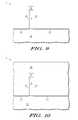
- FIG. 5Shown in FIG. 5 is semiconductor device 10 during a decoupled plasma nitridation (DPN) step 20 .
- DPNdecoupled plasma nitridation
- Thisis a process which separates nitrogen (N 2 ) into free radicals whereby energetic nitrogen atoms are vertically directed toward the surface of oxide layer 12 .
- N 2nitrogen
- 2000 wattsis generally the maximum power and that may be used for it is low enough to avoid very much depth of penetration.
- the desired depth for peak concentrationis about 0.5 nanometer.
- FIG. 6Shown FIG. 6 is semiconductor device 10 after an anneal which converts the combination of oxide and nitrogen to an oxynitride layer 22 along the surface of oxide layer 12 adjacent to fin 14 .
- Oxynitride layer 22preferably is nitrogen rich for about the first 0.5 nanometers from the surface and then reduces in nitrogen content.
- Oxynitride layer 22preferably becomes oxygen rich at least by 2.0 nanometers below the surface.
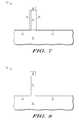
- FIG. 7Shown in FIG. 7 is semiconductor device 10 after growing a thin oxide layer 24 that may be about 2.0 nanometers thick around fin 14 .
- This oxide growthneither occurs on oxynitride layer 22 nor hard mask layer 16 .
- Oxide layer 24is for passivating the damage done to the surface of fin 14 during the etch where semiconductor layer 14 is patterned to form fin 14 .
- the amount of silicon of fin 14 that is consumed in the growthis about 1.0 nanometer.
- the resultis that the vertical surface of fin 14 is substantially aligned to the edge of oxynitride layer 22 .
- semiconductor device 10after removing oxide layer 24 .
- Thisis preferably performed with a wet etch such as hydrofluoric acid (HF).
- HFhydrofluoric acid
- the HFalso is in contact with oxynitride layer 22 .
- Oxynitride layer 22protects oxide layer 12 from the HF.
- the removal of oxide layer 24does not cause etching into oxide layer 12 and particularly prevents undercutting fin 14 . This avoids the possibility of stringers forming in an undercut under fin 14 .
- the removal of oxide layerleaves the sides of fin 14 in an undamaged condition.
- Gate dielectric 26may be an oxide grown at a relatively high temperature. With the sides of fin 14 being undamaged, gate dielectric 26 can be grown with high quality and may be quite thin. In this example, gate dielectric 26 may be 2.0 nanometers. As an alternative, gate dielectric 26 may be a high K dielectric and would be deposited. Even if gate dielectric 26 is a high K material, it is still beneficial for the sides of fin 14 to be as undamaged as possible.
- Gate material 28may be polysilicon and formed by a deposition followed by a step of chemical mechanical polishing (CMP). Gate material 28 may instead be a metal or a combination of conductive materials.
- CMPchemical mechanical polishing
- FIG. 11Shown in FIG. 11 is semiconductor device 10 after patterning gate material 28 to form a gate.
- the patterning as shown in FIG. 11shows a side of a gate that is an end point of the gate formed from patterning gate material 28 .
- FIG. 12Shown in FIG. 12 is semiconductor device 10 after forming a protective layer 31 around gate material 28 , including the side of the gate.
- Protective layer 31may be a deposited oxide so it extends over oxynitride layer 22 adjacent to the side of the gate.
- Protective layer 31may be oxide of about 5.0 nanometers in thickness.
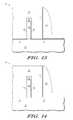
- FIG. 13Shown in FIG. 13 is semiconductor device 10 after forming a sidewall spacer 32 along the side of the gate.
- Sidewall spacer 32may be nitride.
- Sidewall spacer 32is useful in providing a mask for source/drain formation.
- FIG. 14Shown in FIG. 14 is semiconductor device 10 after removing protective layer 31 adjacent to the sidewall spacer 32 .
- Protective layer 31at the time of deposition is formed over areas that may require subsequent silicidation. In such case it is preferable that protective layer 31 be removed from those areas to be silicided without requiring a mask. Without using a mask, exposed protective layer 31 adjacent to sidewall spacer 32 is removed.
- protective layer 31being an oxide, which is the typical case, oxynitride layer 22 protects oxide layer 12 from being etched during the removal of the exposed portion of protective layer 31 .
- oxide layer 12Although likely to be less of a problem than undercutting fin 14 , it is still preferable that oxide layer 12 not be etched during the removal of the exposed portion of protective layer 31 .
- Oxynitride layer 22is thus useful for protecting oxide layer 14 from both the preparation for the gate dielectric formation and the removal of protective layer 31 .
- the methodincludes etching the semiconductor material layer to form a vertical semiconductor material structure overlying the BOX layer, leaving an exposed portion of the BOX layer.
- the methodfurther includes exposing a top surface of the exposed portion of the BOX layer to an oxide etch resistant species to form a thin oxide etch resistant layer overlying the exposed portion of the BOX layer.
- the methodmay further include forming a hard mask layer overlying the semiconductor material layer, forming a patterned photo resist layer overlying the hard mask layer, and using the patterned photo resist layer etching the hard mask layer to form a hard mask.
- the methodmay be further characterized by the etching the semiconductor material layer comprising using the hard mask to form the vertical semiconductor material structure overlying the BOX layer.
- the methodmay be further characterized by the vertical semiconductor material structure being a fin structure corresponding to a FinFET transistor.
- the methodmay be further characterized by the oxide etch resistant layer including Nitrogen.
- the methodmay be further characterized by the exposing step including exposing the exposed portion of the BOX layer to Nitrogen in a radio frequency plasma chamber.
- the methodmay be further characterized by the exposing step including using a decoupled plasma nitridation (DPN) process to expose the exposed portion of the BOX layer to Nitrogen.
- DPNdecoupled plasma nitridation
- the methodmay further include forming a sacrificial oxide layer on at least an exposed surface of the vertical semiconductor material structure and performing a hydro-fluoride (HF) clean to substantially remove the sacrificial oxide layer, wherein the thin oxide etch resistant layer protects the exposed portion of the BOX layer from the HF clean.
- the methodmay be further characterized by the exposing step being performed in a manner such that the thin oxide etch resistant layer has a thickness of less than 20 nanometers.
- the methodmay be further characterized by the exposing step being performed in a manner such that the thin oxide etch resistant layer has a Nitrogen concentration profile such that a top portion of the thin oxide etch resistant layer has a significantly higher concentration of Nitrogen than a bottom portion of the thin oxide etch resistant layer.
- the methodmay be further characterized by the exposing step being performed in a manner such that the thin oxide etch resistant layer has sufficient thickness to protect the underlying BOX layer from erosion caused by a subsequent wet cleaning steps.
- the methodincludes forming a hard mask layer overlying the semiconductor material layer.
- the methodfurther includes forming a patterned photo resist layer overlying the hard mask layer.
- the methodfurther includes using the patterned photo resist layer, etching the hard mask layer to form a hard mask.
- the methodfurther includes etching the semiconductor material layer, except for a portion of the semiconductor material layer underlying the hard mask to form a vertical semiconductor material structure overlying the BOX layer, leaving an exposed portion of the BOX layer.
- the methodfurther includes exposing a top surface of the exposed portion of the BOX layer to Nitrogen to form a thin oxide etch resistant layer overlying the exposed portion of the BOX layer.
- the methodfurther includes forming a sacrificial oxide layer on at least an exposed surface of the vertical semiconductor material structure.
- the methodfurther includes performing a hydro-fluoride (HF) clean to substantially remove the sacrificial oxide layer, wherein the thin oxide etch resistant layer protects the exposed portion of the BOX layer from the HF clean.
- the methodmay be further characterized by the vertical semiconductor material structure being a fin structure corresponding to a FinFET transistor.
- the methodmay be further characterized by the exposing step including exposing the exposed portion of the BOX layer to Nitrogen in a radio frequency plasma chamber.
- the methodmay be further characterized by the exposing step including using a decoupled plasma nitridation (DPN) process to expose the exposed portion of the BOX layer to Nitrogen.
- the methodmay be further characterized by the exposing step being performed in a manner such that the thin oxide etch resistant layer has a thickness of less than 20 nanometers.
- the methodmay be further characterized by the exposing step being performed in a manner such that the thin oxide etch resistant layer has a Nitrogen density concentration such that a top portion of the thin oxide etch resistant layer has a significantly higher concentration of Nitrogen than a bottom portion of the thin oxide etch resistant layer.
- the methodmay be further characterized by the exposing step being performed in a manner such that the thin oxide etch resistant layer has sufficient thickness to protect the underlying BOX layer from erosion caused by a subsequent wet cleaning steps.
- a semiconductor deviceformed using a wafer having a buried oxide (BOX) layer and a semiconductor material layer.
- the semiconductor deviceincludes a vertical semiconductor material structure formed overlying the BOX layer.
- the semiconductor devicefurther includes a thin oxide etch resistant layer formed over an exposed portion of the BOX layer, wherein the thin oxide etch resistant layer is formed to protect a portion of the BOX layer substantially underlying the vertical semiconductor material structure.
- the semiconductor devicemay further include a gate dielectric layer formed around at least a portion of the vertical semiconductor material structure, a gate material structure formed around at least a portion of the gate dielectric layer, a liner formed adjacent the gate material structure, wherein the liner is formed overlying an exposed portion of the thin oxide etch resistant layer, and a spacer formed adjacent the liner.
- the gateis shown as being over hard mask layer 16 , but hard mask layer 16 could be removed at a time prior to forming the gate dielectric. Accordingly, the specification and figures are to be regarded in an illustrative rather than a restrictive sense, and all such modifications are intended to be included within the scope of the present invention. Any benefits, advantages, or solutions to problems that are described herein with regard to specific embodiments are not intended to be construed as a critical, required, or essential feature or element of any or all the claims.
- Coupledis not intended to be limited to a direct coupling or a mechanical coupling.
Landscapes
- Engineering & Computer Science (AREA)
- Physics & Mathematics (AREA)
- Condensed Matter Physics & Semiconductors (AREA)
- General Physics & Mathematics (AREA)
- Manufacturing & Machinery (AREA)
- Computer Hardware Design (AREA)
- Microelectronics & Electronic Packaging (AREA)
- Power Engineering (AREA)
- Drying Of Semiconductors (AREA)
- Thin Film Transistor (AREA)
Abstract
Description
Claims (20)
Priority Applications (1)
| Application Number | Priority Date | Filing Date | Title |
|---|---|---|---|
| US12/130,158US7910482B2 (en) | 2008-05-30 | 2008-05-30 | Method of forming a finFET and structure |
Applications Claiming Priority (1)
| Application Number | Priority Date | Filing Date | Title |
|---|---|---|---|
| US12/130,158US7910482B2 (en) | 2008-05-30 | 2008-05-30 | Method of forming a finFET and structure |
Publications (2)
| Publication Number | Publication Date |
|---|---|
| US20090294919A1 US20090294919A1 (en) | 2009-12-03 |
| US7910482B2true US7910482B2 (en) | 2011-03-22 |
Family
ID=41378747
Family Applications (1)
| Application Number | Title | Priority Date | Filing Date |
|---|---|---|---|
| US12/130,158Expired - Fee RelatedUS7910482B2 (en) | 2008-05-30 | 2008-05-30 | Method of forming a finFET and structure |
Country Status (1)
| Country | Link |
|---|---|
| US (1) | US7910482B2 (en) |
Cited By (6)
| Publication number | Priority date | Publication date | Assignee | Title |
|---|---|---|---|---|
| US20130115777A1 (en)* | 2011-11-09 | 2013-05-09 | Yu-Cheng Tung | Manufacturing method for semiconductor structures |
| US8697536B1 (en) | 2012-11-27 | 2014-04-15 | International Business Machines Corporation | Locally isolated protected bulk finfet semiconductor device |
| US9053965B2 (en)* | 2013-03-14 | 2015-06-09 | International Business Machines Corporation | Partially isolated Fin-shaped field effect transistors |
| US9312273B2 (en) | 2013-12-02 | 2016-04-12 | International Business Machines Corporation | Structure and method to reduce crystal defects in epitaxial fin merge using nitride deposition |
| US9496282B2 (en) | 2013-12-02 | 2016-11-15 | International Business Machines Corporation | Structure and method to reduce crystal defects in epitaxial fin merge using nitride deposition |
| US9530659B2 (en) | 2014-05-02 | 2016-12-27 | International Business Machines Corporation | Structure for preventing buried oxide gouging during planar and FinFET Processing on SOI |
Families Citing this family (4)
| Publication number | Priority date | Publication date | Assignee | Title |
|---|---|---|---|---|
| TWI509709B (en)* | 2011-11-08 | 2015-11-21 | United Microelectronics Corp | Manufacturing method for semiconductor structures |
| US9755033B2 (en)* | 2014-06-13 | 2017-09-05 | Taiwan Semiconductor Manufacturing Co., Ltd. | Semiconductor device and method of forming vertical structure |
| US9324843B2 (en)* | 2014-09-05 | 2016-04-26 | International Business Machines Corporation | High germanium content silicon germanium fins |
| US9680018B2 (en) | 2015-09-21 | 2017-06-13 | International Business Machines Corporation | Method of forming high-germanium content silicon germanium alloy fins on insulator |
Citations (11)
| Publication number | Priority date | Publication date | Assignee | Title |
|---|---|---|---|---|
| US6583469B1 (en) | 2002-01-28 | 2003-06-24 | International Business Machines Corporation | Self-aligned dog-bone structure for FinFET applications and methods to fabricate the same |
| US6716685B2 (en)* | 2002-08-09 | 2004-04-06 | Micron Technology, Inc. | Methods for forming dual gate oxides |
| US6740549B1 (en)* | 2001-08-10 | 2004-05-25 | Integrated Device Technology, Inc. | Gate structures having sidewall spacers using selective deposition and method of forming the same |
| US6835609B1 (en) | 2003-09-17 | 2004-12-28 | Chartered Semiconductor Manufacturing Ltd. | Method of forming double-gate semiconductor-on-insulator (SOI) transistors |
| US6844238B2 (en) | 2003-03-26 | 2005-01-18 | Taiwan Semiconductor Manufacturing Co., Ltd | Multiple-gate transistors with improved gate control |
| US20050026429A1 (en) | 2003-08-01 | 2005-02-03 | Jhon-Jhy Liaw | Method and apparatus for providing an integrated active region on silicon-on-insulator devices |
| US6962843B2 (en)* | 2003-11-05 | 2005-11-08 | International Business Machines Corporation | Method of fabricating a finfet |
| US20060043502A1 (en)* | 2003-11-26 | 2006-03-02 | International Business Machines Corporation | Structure and method to fabricate finfet devices |
| US20060138552A1 (en)* | 2004-09-30 | 2006-06-29 | Brask Justin K | Nonplanar transistors with metal gate electrodes |
| US20070172996A1 (en)* | 2006-01-25 | 2007-07-26 | Leo Mathew | Method of forming a semiconductor device with decreased undercutting of semiconductor material |
| US20080171407A1 (en)* | 2007-01-17 | 2008-07-17 | Tokyo Electron Limited | Manufacturing method of fin-type field effect transistor |
- 2008
- 2008-05-30USUS12/130,158patent/US7910482B2/ennot_activeExpired - Fee Related
Patent Citations (13)
| Publication number | Priority date | Publication date | Assignee | Title |
|---|---|---|---|---|
| US6740549B1 (en)* | 2001-08-10 | 2004-05-25 | Integrated Device Technology, Inc. | Gate structures having sidewall spacers using selective deposition and method of forming the same |
| US6812075B2 (en) | 2002-01-28 | 2004-11-02 | International Business Machines Corporation | Self-aligned dog-bone structure for FinFET applications and methods to fabricate the same |
| US6583469B1 (en) | 2002-01-28 | 2003-06-24 | International Business Machines Corporation | Self-aligned dog-bone structure for FinFET applications and methods to fabricate the same |
| US6716685B2 (en)* | 2002-08-09 | 2004-04-06 | Micron Technology, Inc. | Methods for forming dual gate oxides |
| US6844238B2 (en) | 2003-03-26 | 2005-01-18 | Taiwan Semiconductor Manufacturing Co., Ltd | Multiple-gate transistors with improved gate control |
| US20050026429A1 (en) | 2003-08-01 | 2005-02-03 | Jhon-Jhy Liaw | Method and apparatus for providing an integrated active region on silicon-on-insulator devices |
| US6835609B1 (en) | 2003-09-17 | 2004-12-28 | Chartered Semiconductor Manufacturing Ltd. | Method of forming double-gate semiconductor-on-insulator (SOI) transistors |
| US6962843B2 (en)* | 2003-11-05 | 2005-11-08 | International Business Machines Corporation | Method of fabricating a finfet |
| US20060043502A1 (en)* | 2003-11-26 | 2006-03-02 | International Business Machines Corporation | Structure and method to fabricate finfet devices |
| US20060138552A1 (en)* | 2004-09-30 | 2006-06-29 | Brask Justin K | Nonplanar transistors with metal gate electrodes |
| US20070172996A1 (en)* | 2006-01-25 | 2007-07-26 | Leo Mathew | Method of forming a semiconductor device with decreased undercutting of semiconductor material |
| US7323373B2 (en) | 2006-01-25 | 2008-01-29 | Freescale Semiconductor, Inc. | Method of forming a semiconductor device with decreased undercutting of semiconductor material |
| US20080171407A1 (en)* | 2007-01-17 | 2008-07-17 | Tokyo Electron Limited | Manufacturing method of fin-type field effect transistor |
Cited By (11)
| Publication number | Priority date | Publication date | Assignee | Title |
|---|---|---|---|---|
| US20130115777A1 (en)* | 2011-11-09 | 2013-05-09 | Yu-Cheng Tung | Manufacturing method for semiconductor structures |
| US8546202B2 (en)* | 2011-11-09 | 2013-10-01 | United Microelectronics Corp. | Manufacturing method for semiconductor structures |
| US8697536B1 (en) | 2012-11-27 | 2014-04-15 | International Business Machines Corporation | Locally isolated protected bulk finfet semiconductor device |
| US8975675B2 (en) | 2012-11-27 | 2015-03-10 | International Business Machines Corporation | Locally isolated protected bulk FinFET semiconductor device |
| US9299617B2 (en) | 2012-11-27 | 2016-03-29 | Globalfoundries Inc. | Locally isolated protected bulk FinFET semiconductor device |
| US9053965B2 (en)* | 2013-03-14 | 2015-06-09 | International Business Machines Corporation | Partially isolated Fin-shaped field effect transistors |
| US9634000B2 (en) | 2013-03-14 | 2017-04-25 | International Business Machines Corporation | Partially isolated fin-shaped field effect transistors |
| US9312273B2 (en) | 2013-12-02 | 2016-04-12 | International Business Machines Corporation | Structure and method to reduce crystal defects in epitaxial fin merge using nitride deposition |
| US9472576B2 (en) | 2013-12-02 | 2016-10-18 | International Business Machines Corporation | Structure and method to reduce crystal defects in epitaxial fin merge using nitride deposition |
| US9496282B2 (en) | 2013-12-02 | 2016-11-15 | International Business Machines Corporation | Structure and method to reduce crystal defects in epitaxial fin merge using nitride deposition |
| US9530659B2 (en) | 2014-05-02 | 2016-12-27 | International Business Machines Corporation | Structure for preventing buried oxide gouging during planar and FinFET Processing on SOI |
Also Published As
| Publication number | Publication date |
|---|---|
| US20090294919A1 (en) | 2009-12-03 |
Similar Documents
| Publication | Publication Date | Title |
|---|---|---|
| US7910482B2 (en) | Method of forming a finFET and structure | |
| US9190518B2 (en) | Nonplanar device with thinned lower body portion and method of fabrication | |
| US7265059B2 (en) | Multiple fin formation | |
| US20110298098A1 (en) | Expitaxial fabrication of fins for finfet devices | |
| US20070210357A1 (en) | Mosfet having recessed channel and method of fabricating the same | |
| US20150380251A1 (en) | Block mask litho on high aspect ratio topography with minimal semiconductor material damage | |
| US20050127459A1 (en) | Novel gate structure and method of forming the gate dielectric with mini-spacer | |
| US7015089B2 (en) | Method to improve etching of resist protective oxide (RPO) to prevent photo-resist peeling | |
| US6727150B2 (en) | Methods of forming trench isolation within a semiconductor substrate including, Tshaped trench with spacers | |
| US6107140A (en) | Method of patterning gate electrode conductor with ultra-thin gate oxide | |
| US20060046487A1 (en) | Method of manufacturing a semiconductor device, and a semiconductor substrate | |
| US7611950B2 (en) | Method for forming shallow trench isolation in semiconductor device | |
| CN112151382B (en) | Semiconductor structure and forming method thereof | |
| JP2003197731A (en) | Method for forming isolation film of semiconductor element | |
| US20050170597A1 (en) | Semiconductor apparatus and method of manufacturing the same | |
| CN104701262B (en) | A kind of forming method of semiconductor devices | |
| JP2010021240A (en) | Manufacturing method of semiconductor device | |
| US6927106B2 (en) | Methods for fabricating a triple-gate MOSFET transistor | |
| CN100401530C (en) | Method for forming strained channel element | |
| US7416988B2 (en) | Semiconductor device and fabrication process thereof | |
| CN1197132C (en) | Wet chemical removal of silicon oxynitride material after gate etch process | |
| TWI879712B (en) | Semiconductor device and fabrication method thereof | |
| CN112635324B (en) | Semiconductor structure and forming method thereof | |
| JP3053009B2 (en) | Method for manufacturing semiconductor device | |
| CN109841527B (en) | Semiconductor structure and forming method thereof |
Legal Events
| Date | Code | Title | Description |
|---|---|---|---|
| AS | Assignment | Owner name:FREESCALE SEMICONDUCTOR, INC.,TEXAS Free format text:ASSIGNMENT OF ASSIGNORS INTEREST;ASSIGNORS:STEPHENS, TAB A.;MATHEW, LEO;VISHNUBHOLTA, LAKSHMANNA;AND OTHERS;SIGNING DATES FROM 20080523 TO 20080530;REEL/FRAME:021106/0806 Owner name:FREESCALE SEMICONDUCTOR, INC., TEXAS Free format text:ASSIGNMENT OF ASSIGNORS INTEREST;ASSIGNORS:STEPHENS, TAB A.;MATHEW, LEO;VISHNUBHOLTA, LAKSHMANNA;AND OTHERS;SIGNING DATES FROM 20080523 TO 20080530;REEL/FRAME:021106/0806 | |
| AS | Assignment | Owner name:CITIBANK, N.A.,NEW YORK Free format text:SECURITY AGREEMENT;ASSIGNOR:FREESCALE SEMICONDUCTOR, INC.;REEL/FRAME:021570/0449 Effective date:20080728 Owner name:CITIBANK, N.A., NEW YORK Free format text:SECURITY AGREEMENT;ASSIGNOR:FREESCALE SEMICONDUCTOR, INC.;REEL/FRAME:021570/0449 Effective date:20080728 | |
| AS | Assignment | Owner name:CITIBANK, N.A.,NEW YORK Free format text:SECURITY AGREEMENT;ASSIGNOR:FREESCALE SEMICONDUCTOR, INC.;REEL/FRAME:024085/0001 Effective date:20100219 Owner name:CITIBANK, N.A., NEW YORK Free format text:SECURITY AGREEMENT;ASSIGNOR:FREESCALE SEMICONDUCTOR, INC.;REEL/FRAME:024085/0001 Effective date:20100219 | |
| AS | Assignment | Owner name:CITIBANK, N.A., AS COLLATERAL AGENT,NEW YORK Free format text:SECURITY AGREEMENT;ASSIGNOR:FREESCALE SEMICONDUCTOR, INC.;REEL/FRAME:024397/0001 Effective date:20100413 Owner name:CITIBANK, N.A., AS COLLATERAL AGENT, NEW YORK Free format text:SECURITY AGREEMENT;ASSIGNOR:FREESCALE SEMICONDUCTOR, INC.;REEL/FRAME:024397/0001 Effective date:20100413 | |
| STCF | Information on status: patent grant | Free format text:PATENTED CASE | |
| AS | Assignment | Owner name:CITIBANK, N.A., AS NOTES COLLATERAL AGENT, NEW YORK Free format text:SECURITY AGREEMENT;ASSIGNOR:FREESCALE SEMICONDUCTOR, INC.;REEL/FRAME:030633/0424 Effective date:20130521 Owner name:CITIBANK, N.A., AS NOTES COLLATERAL AGENT, NEW YOR Free format text:SECURITY AGREEMENT;ASSIGNOR:FREESCALE SEMICONDUCTOR, INC.;REEL/FRAME:030633/0424 Effective date:20130521 | |
| AS | Assignment | Owner name:CITIBANK, N.A., AS NOTES COLLATERAL AGENT, NEW YORK Free format text:SECURITY AGREEMENT;ASSIGNOR:FREESCALE SEMICONDUCTOR, INC.;REEL/FRAME:031591/0266 Effective date:20131101 Owner name:CITIBANK, N.A., AS NOTES COLLATERAL AGENT, NEW YOR Free format text:SECURITY AGREEMENT;ASSIGNOR:FREESCALE SEMICONDUCTOR, INC.;REEL/FRAME:031591/0266 Effective date:20131101 | |
| FPAY | Fee payment | Year of fee payment:4 | |
| AS | Assignment | Owner name:FREESCALE SEMICONDUCTOR, INC., TEXAS Free format text:PATENT RELEASE;ASSIGNOR:CITIBANK, N.A., AS COLLATERAL AGENT;REEL/FRAME:037356/0553 Effective date:20151207 Owner name:FREESCALE SEMICONDUCTOR, INC., TEXAS Free format text:PATENT RELEASE;ASSIGNOR:CITIBANK, N.A., AS COLLATERAL AGENT;REEL/FRAME:037354/0719 Effective date:20151207 Owner name:FREESCALE SEMICONDUCTOR, INC., TEXAS Free format text:PATENT RELEASE;ASSIGNOR:CITIBANK, N.A., AS COLLATERAL AGENT;REEL/FRAME:037356/0143 Effective date:20151207 | |
| AS | Assignment | Owner name:MORGAN STANLEY SENIOR FUNDING, INC., MARYLAND Free format text:ASSIGNMENT AND ASSUMPTION OF SECURITY INTEREST IN PATENTS;ASSIGNOR:CITIBANK, N.A.;REEL/FRAME:037486/0517 Effective date:20151207 | |
| AS | Assignment | Owner name:MORGAN STANLEY SENIOR FUNDING, INC., MARYLAND Free format text:ASSIGNMENT AND ASSUMPTION OF SECURITY INTEREST IN PATENTS;ASSIGNOR:CITIBANK, N.A.;REEL/FRAME:037518/0292 Effective date:20151207 | |
| AS | Assignment | Owner name:NORTH STAR INNOVATIONS INC., CALIFORNIA Free format text:ASSIGNMENT OF ASSIGNORS INTEREST;ASSIGNOR:FREESCALE SEMICONDUCTOR, INC.;REEL/FRAME:037694/0264 Effective date:20151002 | |
| AS | Assignment | Owner name:NXP, B.V., F/K/A FREESCALE SEMICONDUCTOR, INC., NETHERLANDS Free format text:RELEASE BY SECURED PARTY;ASSIGNOR:MORGAN STANLEY SENIOR FUNDING, INC.;REEL/FRAME:040925/0001 Effective date:20160912 Owner name:NXP, B.V., F/K/A FREESCALE SEMICONDUCTOR, INC., NE Free format text:RELEASE BY SECURED PARTY;ASSIGNOR:MORGAN STANLEY SENIOR FUNDING, INC.;REEL/FRAME:040925/0001 Effective date:20160912 | |
| AS | Assignment | Owner name:NXP B.V., NETHERLANDS Free format text:RELEASE BY SECURED PARTY;ASSIGNOR:MORGAN STANLEY SENIOR FUNDING, INC.;REEL/FRAME:040928/0001 Effective date:20160622 | |
| AS | Assignment | Owner name:MORGAN STANLEY SENIOR FUNDING, INC., MARYLAND Free format text:CORRECTIVE ASSIGNMENT TO CORRECT THE REMOVE PATENTS 8108266 AND 8062324 AND REPLACE THEM WITH 6108266 AND 8060324 PREVIOUSLY RECORDED ON REEL 037518 FRAME 0292. ASSIGNOR(S) HEREBY CONFIRMS THE ASSIGNMENT AND ASSUMPTION OF SECURITY INTEREST IN PATENTS;ASSIGNOR:CITIBANK, N.A.;REEL/FRAME:041703/0536 Effective date:20151207 | |
| AS | Assignment | Owner name:TAIWAN SEMICONDUCTOR MANUFACTURING CO., LTD., TAIW Free format text:ASSIGNMENT OF ASSIGNORS INTEREST;ASSIGNOR:NORTH STAR INNOVATIONS INC.;REEL/FRAME:041717/0736 Effective date:20161006 | |
| FEPP | Fee payment procedure | Free format text:MAINTENANCE FEE REMINDER MAILED (ORIGINAL EVENT CODE: REM.); ENTITY STATUS OF PATENT OWNER: LARGE ENTITY | |
| AS | Assignment | Owner name:SHENZHEN XINGUODU TECHNOLOGY CO., LTD., CHINA Free format text:CORRECTIVE ASSIGNMENT TO CORRECT THE TO CORRECT THE APPLICATION NO. FROM 13,883,290 TO 13,833,290 PREVIOUSLY RECORDED ON REEL 041703 FRAME 0536. ASSIGNOR(S) HEREBY CONFIRMS THE THE ASSIGNMENT AND ASSUMPTION OF SECURITYINTEREST IN PATENTS.;ASSIGNOR:MORGAN STANLEY SENIOR FUNDING, INC.;REEL/FRAME:048734/0001 Effective date:20190217 | |
| LAPS | Lapse for failure to pay maintenance fees | Free format text:PATENT EXPIRED FOR FAILURE TO PAY MAINTENANCE FEES (ORIGINAL EVENT CODE: EXP.); ENTITY STATUS OF PATENT OWNER: LARGE ENTITY | |
| STCH | Information on status: patent discontinuation | Free format text:PATENT EXPIRED DUE TO NONPAYMENT OF MAINTENANCE FEES UNDER 37 CFR 1.362 | |
| FP | Lapsed due to failure to pay maintenance fee | Effective date:20190322 | |
| AS | Assignment | Owner name:TAIWAN SEMICONDUCTOR MANUFACTURING CO., LTD., TAIWAN Free format text:323.01(C) ASSIGNMENT OR CHANGE OF NAME IMPROPERLY FILED AND RECORDED BY ANOTHER PERSON AGAINST OWNER'S PATENT;ASSIGNOR:TAIWAN SEMICONDUCTOR MANUFACTURING CO., LTD.;REEL/FRAME:052459/0656 Effective date:20190924 | |
| AS | Assignment | Owner name:MORGAN STANLEY SENIOR FUNDING, INC., MARYLAND Free format text:CORRECTIVE ASSIGNMENT TO CORRECT THE REMOVE APPLICATION11759915 AND REPLACE IT WITH APPLICATION 11759935 PREVIOUSLY RECORDED ON REEL 037486 FRAME 0517. ASSIGNOR(S) HEREBY CONFIRMS THE ASSIGNMENT AND ASSUMPTION OF SECURITYINTEREST IN PATENTS;ASSIGNOR:CITIBANK, N.A.;REEL/FRAME:053547/0421 Effective date:20151207 | |
| AS | Assignment | Owner name:NXP B.V., NETHERLANDS Free format text:CORRECTIVE ASSIGNMENT TO CORRECT THE REMOVEAPPLICATION 11759915 AND REPLACE IT WITH APPLICATION11759935 PREVIOUSLY RECORDED ON REEL 040928 FRAME 0001. ASSIGNOR(S) HEREBY CONFIRMS THE RELEASE OF SECURITYINTEREST;ASSIGNOR:MORGAN STANLEY SENIOR FUNDING, INC.;REEL/FRAME:052915/0001 Effective date:20160622 | |
| AS | Assignment | Owner name:NXP, B.V. F/K/A FREESCALE SEMICONDUCTOR, INC., NETHERLANDS Free format text:CORRECTIVE ASSIGNMENT TO CORRECT THE REMOVEAPPLICATION 11759915 AND REPLACE IT WITH APPLICATION11759935 PREVIOUSLY RECORDED ON REEL 040925 FRAME 0001. ASSIGNOR(S) HEREBY CONFIRMS THE RELEASE OF SECURITYINTEREST;ASSIGNOR:MORGAN STANLEY SENIOR FUNDING, INC.;REEL/FRAME:052917/0001 Effective date:20160912 |