US7910392B2 - Method and system for assembling a solar cell package - Google Patents
Method and system for assembling a solar cell packageDownload PDFInfo
- Publication number
- US7910392B2 US7910392B2US12/060,801US6080108AUS7910392B2US 7910392 B2US7910392 B2US 7910392B2US 6080108 AUS6080108 AUS 6080108AUS 7910392 B2US7910392 B2US 7910392B2
- Authority
- US
- United States
- Prior art keywords
- region
- substrate member
- substrate
- peripheral region
- solar cell
- Prior art date
- Legal status (The legal status is an assumption and is not a legal conclusion. Google has not performed a legal analysis and makes no representation as to the accuracy of the status listed.)
- Expired - Fee Related, expires
Links
Images


Classifications
- H—ELECTRICITY
- H10—SEMICONDUCTOR DEVICES; ELECTRIC SOLID-STATE DEVICES NOT OTHERWISE PROVIDED FOR
- H10F—INORGANIC SEMICONDUCTOR DEVICES SENSITIVE TO INFRARED RADIATION, LIGHT, ELECTROMAGNETIC RADIATION OF SHORTER WAVELENGTH OR CORPUSCULAR RADIATION
- H10F19/00—Integrated devices, or assemblies of multiple devices, comprising at least one photovoltaic cell covered by group H10F10/00, e.g. photovoltaic modules
- H10F19/80—Encapsulations or containers for integrated devices, or assemblies of multiple devices, having photovoltaic cells
- B—PERFORMING OPERATIONS; TRANSPORTING
- B23—MACHINE TOOLS; METAL-WORKING NOT OTHERWISE PROVIDED FOR
- B23K—SOLDERING OR UNSOLDERING; WELDING; CLADDING OR PLATING BY SOLDERING OR WELDING; CUTTING BY APPLYING HEAT LOCALLY, e.g. FLAME CUTTING; WORKING BY LASER BEAM
- B23K26/00—Working by laser beam, e.g. welding, cutting or boring
- B23K26/02—Positioning or observing the workpiece, e.g. with respect to the point of impact; Aligning, aiming or focusing the laser beam
- B23K26/06—Shaping the laser beam, e.g. by masks or multi-focusing
- B23K26/064—Shaping the laser beam, e.g. by masks or multi-focusing by means of optical elements, e.g. lenses, mirrors or prisms
- B23K26/066—Shaping the laser beam, e.g. by masks or multi-focusing by means of optical elements, e.g. lenses, mirrors or prisms by using masks
- B23K26/0661—Shaping the laser beam, e.g. by masks or multi-focusing by means of optical elements, e.g. lenses, mirrors or prisms by using masks disposed on the workpiece
- B—PERFORMING OPERATIONS; TRANSPORTING
- B29—WORKING OF PLASTICS; WORKING OF SUBSTANCES IN A PLASTIC STATE IN GENERAL
- B29C—SHAPING OR JOINING OF PLASTICS; SHAPING OF MATERIAL IN A PLASTIC STATE, NOT OTHERWISE PROVIDED FOR; AFTER-TREATMENT OF THE SHAPED PRODUCTS, e.g. REPAIRING
- B29C65/00—Joining or sealing of preformed parts, e.g. welding of plastics materials; Apparatus therefor
- B29C65/02—Joining or sealing of preformed parts, e.g. welding of plastics materials; Apparatus therefor by heating, with or without pressure
- B29C65/14—Joining or sealing of preformed parts, e.g. welding of plastics materials; Apparatus therefor by heating, with or without pressure using wave energy, i.e. electromagnetic radiation, or particle radiation
- B29C65/1429—Joining or sealing of preformed parts, e.g. welding of plastics materials; Apparatus therefor by heating, with or without pressure using wave energy, i.e. electromagnetic radiation, or particle radiation characterised by the way of heating the interface
- B29C65/1435—Joining or sealing of preformed parts, e.g. welding of plastics materials; Apparatus therefor by heating, with or without pressure using wave energy, i.e. electromagnetic radiation, or particle radiation characterised by the way of heating the interface at least passing through one of the parts to be joined, i.e. transmission welding
- B—PERFORMING OPERATIONS; TRANSPORTING
- B29—WORKING OF PLASTICS; WORKING OF SUBSTANCES IN A PLASTIC STATE IN GENERAL
- B29C—SHAPING OR JOINING OF PLASTICS; SHAPING OF MATERIAL IN A PLASTIC STATE, NOT OTHERWISE PROVIDED FOR; AFTER-TREATMENT OF THE SHAPED PRODUCTS, e.g. REPAIRING
- B29C65/00—Joining or sealing of preformed parts, e.g. welding of plastics materials; Apparatus therefor
- B29C65/02—Joining or sealing of preformed parts, e.g. welding of plastics materials; Apparatus therefor by heating, with or without pressure
- B29C65/14—Joining or sealing of preformed parts, e.g. welding of plastics materials; Apparatus therefor by heating, with or without pressure using wave energy, i.e. electromagnetic radiation, or particle radiation
- B29C65/1496—Joining or sealing of preformed parts, e.g. welding of plastics materials; Apparatus therefor by heating, with or without pressure using wave energy, i.e. electromagnetic radiation, or particle radiation making use of masks
- B—PERFORMING OPERATIONS; TRANSPORTING
- B29—WORKING OF PLASTICS; WORKING OF SUBSTANCES IN A PLASTIC STATE IN GENERAL
- B29C—SHAPING OR JOINING OF PLASTICS; SHAPING OF MATERIAL IN A PLASTIC STATE, NOT OTHERWISE PROVIDED FOR; AFTER-TREATMENT OF THE SHAPED PRODUCTS, e.g. REPAIRING
- B29C65/00—Joining or sealing of preformed parts, e.g. welding of plastics materials; Apparatus therefor
- B29C65/02—Joining or sealing of preformed parts, e.g. welding of plastics materials; Apparatus therefor by heating, with or without pressure
- B29C65/14—Joining or sealing of preformed parts, e.g. welding of plastics materials; Apparatus therefor by heating, with or without pressure using wave energy, i.e. electromagnetic radiation, or particle radiation
- B29C65/16—Laser beams
- B29C65/1629—Laser beams characterised by the way of heating the interface
- B29C65/1635—Laser beams characterised by the way of heating the interface at least passing through one of the parts to be joined, i.e. laser transmission welding
- B—PERFORMING OPERATIONS; TRANSPORTING
- B29—WORKING OF PLASTICS; WORKING OF SUBSTANCES IN A PLASTIC STATE IN GENERAL
- B29C—SHAPING OR JOINING OF PLASTICS; SHAPING OF MATERIAL IN A PLASTIC STATE, NOT OTHERWISE PROVIDED FOR; AFTER-TREATMENT OF THE SHAPED PRODUCTS, e.g. REPAIRING
- B29C65/00—Joining or sealing of preformed parts, e.g. welding of plastics materials; Apparatus therefor
- B29C65/02—Joining or sealing of preformed parts, e.g. welding of plastics materials; Apparatus therefor by heating, with or without pressure
- B29C65/14—Joining or sealing of preformed parts, e.g. welding of plastics materials; Apparatus therefor by heating, with or without pressure using wave energy, i.e. electromagnetic radiation, or particle radiation
- B29C65/16—Laser beams
- B29C65/1629—Laser beams characterised by the way of heating the interface
- B29C65/1654—Laser beams characterised by the way of heating the interface scanning at least one of the parts to be joined
- B—PERFORMING OPERATIONS; TRANSPORTING
- B29—WORKING OF PLASTICS; WORKING OF SUBSTANCES IN A PLASTIC STATE IN GENERAL
- B29C—SHAPING OR JOINING OF PLASTICS; SHAPING OF MATERIAL IN A PLASTIC STATE, NOT OTHERWISE PROVIDED FOR; AFTER-TREATMENT OF THE SHAPED PRODUCTS, e.g. REPAIRING
- B29C65/00—Joining or sealing of preformed parts, e.g. welding of plastics materials; Apparatus therefor
- B29C65/02—Joining or sealing of preformed parts, e.g. welding of plastics materials; Apparatus therefor by heating, with or without pressure
- B29C65/14—Joining or sealing of preformed parts, e.g. welding of plastics materials; Apparatus therefor by heating, with or without pressure using wave energy, i.e. electromagnetic radiation, or particle radiation
- B29C65/16—Laser beams
- B29C65/1687—Laser beams making use of light guides
- B—PERFORMING OPERATIONS; TRANSPORTING
- B29—WORKING OF PLASTICS; WORKING OF SUBSTANCES IN A PLASTIC STATE IN GENERAL
- B29C—SHAPING OR JOINING OF PLASTICS; SHAPING OF MATERIAL IN A PLASTIC STATE, NOT OTHERWISE PROVIDED FOR; AFTER-TREATMENT OF THE SHAPED PRODUCTS, e.g. REPAIRING
- B29C65/00—Joining or sealing of preformed parts, e.g. welding of plastics materials; Apparatus therefor
- B29C65/02—Joining or sealing of preformed parts, e.g. welding of plastics materials; Apparatus therefor by heating, with or without pressure
- B29C65/14—Joining or sealing of preformed parts, e.g. welding of plastics materials; Apparatus therefor by heating, with or without pressure using wave energy, i.e. electromagnetic radiation, or particle radiation
- B29C65/16—Laser beams
- B29C65/1696—Laser beams making use of masks
- B—PERFORMING OPERATIONS; TRANSPORTING
- B29—WORKING OF PLASTICS; WORKING OF SUBSTANCES IN A PLASTIC STATE IN GENERAL
- B29C—SHAPING OR JOINING OF PLASTICS; SHAPING OF MATERIAL IN A PLASTIC STATE, NOT OTHERWISE PROVIDED FOR; AFTER-TREATMENT OF THE SHAPED PRODUCTS, e.g. REPAIRING
- B29C65/00—Joining or sealing of preformed parts, e.g. welding of plastics materials; Apparatus therefor
- B29C65/78—Means for handling the parts to be joined, e.g. for making containers or hollow articles, e.g. means for handling sheets, plates, web-like materials, tubular articles, hollow articles or elements to be joined therewith; Means for discharging the joined articles from the joining apparatus
- B29C65/7802—Positioning the parts to be joined, e.g. aligning, indexing or centring
- B29C65/7805—Positioning the parts to be joined, e.g. aligning, indexing or centring the parts to be joined comprising positioning features
- B29C65/7814—Positioning the parts to be joined, e.g. aligning, indexing or centring the parts to be joined comprising positioning features in the form of inter-cooperating positioning features, e.g. tenons and mortises
- B—PERFORMING OPERATIONS; TRANSPORTING
- B29—WORKING OF PLASTICS; WORKING OF SUBSTANCES IN A PLASTIC STATE IN GENERAL
- B29C—SHAPING OR JOINING OF PLASTICS; SHAPING OF MATERIAL IN A PLASTIC STATE, NOT OTHERWISE PROVIDED FOR; AFTER-TREATMENT OF THE SHAPED PRODUCTS, e.g. REPAIRING
- B29C66/00—General aspects of processes or apparatus for joining preformed parts
- B29C66/01—General aspects dealing with the joint area or with the area to be joined
- B29C66/02—Preparation of the material, in the area to be joined, prior to joining or welding
- B29C66/022—Mechanical pre-treatments, e.g. reshaping
- B29C66/0222—Mechanical pre-treatments, e.g. reshaping without removal of material, e.g. cleaning by air blowing or using brushes
- B—PERFORMING OPERATIONS; TRANSPORTING
- B29—WORKING OF PLASTICS; WORKING OF SUBSTANCES IN A PLASTIC STATE IN GENERAL
- B29C—SHAPING OR JOINING OF PLASTICS; SHAPING OF MATERIAL IN A PLASTIC STATE, NOT OTHERWISE PROVIDED FOR; AFTER-TREATMENT OF THE SHAPED PRODUCTS, e.g. REPAIRING
- B29C66/00—General aspects of processes or apparatus for joining preformed parts
- B29C66/01—General aspects dealing with the joint area or with the area to be joined
- B29C66/05—Particular design of joint configurations
- B29C66/10—Particular design of joint configurations particular design of the joint cross-sections
- B29C66/12—Joint cross-sections combining only two joint-segments; Tongue and groove joints; Tenon and mortise joints; Stepped joint cross-sections
- B29C66/124—Tongue and groove joints
- B29C66/1246—Tongue and groove joints characterised by the female part, i.e. the part comprising the groove
- B29C66/12461—Tongue and groove joints characterised by the female part, i.e. the part comprising the groove being rounded, i.e. U-shaped or C-shaped
- B—PERFORMING OPERATIONS; TRANSPORTING
- B29—WORKING OF PLASTICS; WORKING OF SUBSTANCES IN A PLASTIC STATE IN GENERAL
- B29C—SHAPING OR JOINING OF PLASTICS; SHAPING OF MATERIAL IN A PLASTIC STATE, NOT OTHERWISE PROVIDED FOR; AFTER-TREATMENT OF THE SHAPED PRODUCTS, e.g. REPAIRING
- B29C66/00—General aspects of processes or apparatus for joining preformed parts
- B29C66/01—General aspects dealing with the joint area or with the area to be joined
- B29C66/05—Particular design of joint configurations
- B29C66/10—Particular design of joint configurations particular design of the joint cross-sections
- B29C66/12—Joint cross-sections combining only two joint-segments; Tongue and groove joints; Tenon and mortise joints; Stepped joint cross-sections
- B29C66/124—Tongue and groove joints
- B29C66/1246—Tongue and groove joints characterised by the female part, i.e. the part comprising the groove
- B29C66/12463—Tongue and groove joints characterised by the female part, i.e. the part comprising the groove being tapered
- B—PERFORMING OPERATIONS; TRANSPORTING
- B29—WORKING OF PLASTICS; WORKING OF SUBSTANCES IN A PLASTIC STATE IN GENERAL
- B29C—SHAPING OR JOINING OF PLASTICS; SHAPING OF MATERIAL IN A PLASTIC STATE, NOT OTHERWISE PROVIDED FOR; AFTER-TREATMENT OF THE SHAPED PRODUCTS, e.g. REPAIRING
- B29C66/00—General aspects of processes or apparatus for joining preformed parts
- B29C66/01—General aspects dealing with the joint area or with the area to be joined
- B29C66/05—Particular design of joint configurations
- B29C66/20—Particular design of joint configurations particular design of the joint lines, e.g. of the weld lines
- B29C66/24—Particular design of joint configurations particular design of the joint lines, e.g. of the weld lines said joint lines being closed or non-straight
- B29C66/242—Particular design of joint configurations particular design of the joint lines, e.g. of the weld lines said joint lines being closed or non-straight said joint lines being closed, i.e. forming closed contours
- B29C66/2424—Particular design of joint configurations particular design of the joint lines, e.g. of the weld lines said joint lines being closed or non-straight said joint lines being closed, i.e. forming closed contours being a closed polygonal chain
- B29C66/24243—Particular design of joint configurations particular design of the joint lines, e.g. of the weld lines said joint lines being closed or non-straight said joint lines being closed, i.e. forming closed contours being a closed polygonal chain forming a quadrilateral
- B29C66/24244—Particular design of joint configurations particular design of the joint lines, e.g. of the weld lines said joint lines being closed or non-straight said joint lines being closed, i.e. forming closed contours being a closed polygonal chain forming a quadrilateral forming a rectangle
- B—PERFORMING OPERATIONS; TRANSPORTING
- B29—WORKING OF PLASTICS; WORKING OF SUBSTANCES IN A PLASTIC STATE IN GENERAL
- B29C—SHAPING OR JOINING OF PLASTICS; SHAPING OF MATERIAL IN A PLASTIC STATE, NOT OTHERWISE PROVIDED FOR; AFTER-TREATMENT OF THE SHAPED PRODUCTS, e.g. REPAIRING
- B29C66/00—General aspects of processes or apparatus for joining preformed parts
- B29C66/01—General aspects dealing with the joint area or with the area to be joined
- B29C66/347—General aspects dealing with the joint area or with the area to be joined using particular temperature distributions or gradients; using particular heat distributions or gradients
- B29C66/3474—General aspects dealing with the joint area or with the area to be joined using particular temperature distributions or gradients; using particular heat distributions or gradients perpendicular to the plane of the joint
- B—PERFORMING OPERATIONS; TRANSPORTING
- B29—WORKING OF PLASTICS; WORKING OF SUBSTANCES IN A PLASTIC STATE IN GENERAL
- B29C—SHAPING OR JOINING OF PLASTICS; SHAPING OF MATERIAL IN A PLASTIC STATE, NOT OTHERWISE PROVIDED FOR; AFTER-TREATMENT OF THE SHAPED PRODUCTS, e.g. REPAIRING
- B29C66/00—General aspects of processes or apparatus for joining preformed parts
- B29C66/50—General aspects of joining tubular articles; General aspects of joining long products, i.e. bars or profiled elements; General aspects of joining single elements to tubular articles, hollow articles or bars; General aspects of joining several hollow-preforms to form hollow or tubular articles
- B29C66/51—Joining tubular articles, profiled elements or bars; Joining single elements to tubular articles, hollow articles or bars; Joining several hollow-preforms to form hollow or tubular articles
- B29C66/54—Joining several hollow-preforms, e.g. half-shells, to form hollow articles, e.g. for making balls, containers; Joining several hollow-preforms, e.g. half-cylinders, to form tubular articles
- B—PERFORMING OPERATIONS; TRANSPORTING
- B29—WORKING OF PLASTICS; WORKING OF SUBSTANCES IN A PLASTIC STATE IN GENERAL
- B29C—SHAPING OR JOINING OF PLASTICS; SHAPING OF MATERIAL IN A PLASTIC STATE, NOT OTHERWISE PROVIDED FOR; AFTER-TREATMENT OF THE SHAPED PRODUCTS, e.g. REPAIRING
- B29C66/00—General aspects of processes or apparatus for joining preformed parts
- B29C66/80—General aspects of machine operations or constructions and parts thereof
- B29C66/83—General aspects of machine operations or constructions and parts thereof characterised by the movement of the joining or pressing tools
- B29C66/832—Reciprocating joining or pressing tools
- B29C66/8322—Joining or pressing tools reciprocating along one axis
- B—PERFORMING OPERATIONS; TRANSPORTING
- B29—WORKING OF PLASTICS; WORKING OF SUBSTANCES IN A PLASTIC STATE IN GENERAL
- B29C—SHAPING OR JOINING OF PLASTICS; SHAPING OF MATERIAL IN A PLASTIC STATE, NOT OTHERWISE PROVIDED FOR; AFTER-TREATMENT OF THE SHAPED PRODUCTS, e.g. REPAIRING
- B29C66/00—General aspects of processes or apparatus for joining preformed parts
- B29C66/90—Measuring or controlling the joining process
- B29C66/91—Measuring or controlling the joining process by measuring or controlling the temperature, the heat or the thermal flux
- B29C66/914—Measuring or controlling the joining process by measuring or controlling the temperature, the heat or the thermal flux by controlling or regulating the temperature, the heat or the thermal flux
- B29C66/9141—Measuring or controlling the joining process by measuring or controlling the temperature, the heat or the thermal flux by controlling or regulating the temperature, the heat or the thermal flux by controlling or regulating the temperature
- B29C66/91411—Measuring or controlling the joining process by measuring or controlling the temperature, the heat or the thermal flux by controlling or regulating the temperature, the heat or the thermal flux by controlling or regulating the temperature of the parts to be joined, e.g. the joining process taking the temperature of the parts to be joined into account
- B—PERFORMING OPERATIONS; TRANSPORTING
- B29—WORKING OF PLASTICS; WORKING OF SUBSTANCES IN A PLASTIC STATE IN GENERAL
- B29C—SHAPING OR JOINING OF PLASTICS; SHAPING OF MATERIAL IN A PLASTIC STATE, NOT OTHERWISE PROVIDED FOR; AFTER-TREATMENT OF THE SHAPED PRODUCTS, e.g. REPAIRING
- B29C66/00—General aspects of processes or apparatus for joining preformed parts
- B29C66/90—Measuring or controlling the joining process
- B29C66/91—Measuring or controlling the joining process by measuring or controlling the temperature, the heat or the thermal flux
- B29C66/919—Measuring or controlling the joining process by measuring or controlling the temperature, the heat or the thermal flux characterised by specific temperature, heat or thermal flux values or ranges
- B29C66/9192—Measuring or controlling the joining process by measuring or controlling the temperature, the heat or the thermal flux characterised by specific temperature, heat or thermal flux values or ranges in explicit relation to another variable, e.g. temperature diagrams
- B—PERFORMING OPERATIONS; TRANSPORTING
- B29—WORKING OF PLASTICS; WORKING OF SUBSTANCES IN A PLASTIC STATE IN GENERAL
- B29C—SHAPING OR JOINING OF PLASTICS; SHAPING OF MATERIAL IN A PLASTIC STATE, NOT OTHERWISE PROVIDED FOR; AFTER-TREATMENT OF THE SHAPED PRODUCTS, e.g. REPAIRING
- B29C66/00—General aspects of processes or apparatus for joining preformed parts
- B29C66/90—Measuring or controlling the joining process
- B29C66/92—Measuring or controlling the joining process by measuring or controlling the pressure, the force, the mechanical power or the displacement of the joining tools
- B29C66/924—Measuring or controlling the joining process by measuring or controlling the pressure, the force, the mechanical power or the displacement of the joining tools by controlling or regulating the pressure, the force, the mechanical power or the displacement of the joining tools
- B29C66/9241—Measuring or controlling the joining process by measuring or controlling the pressure, the force, the mechanical power or the displacement of the joining tools by controlling or regulating the pressure, the force, the mechanical power or the displacement of the joining tools by controlling or regulating the pressure, the force or the mechanical power
- B—PERFORMING OPERATIONS; TRANSPORTING
- B29—WORKING OF PLASTICS; WORKING OF SUBSTANCES IN A PLASTIC STATE IN GENERAL
- B29C—SHAPING OR JOINING OF PLASTICS; SHAPING OF MATERIAL IN A PLASTIC STATE, NOT OTHERWISE PROVIDED FOR; AFTER-TREATMENT OF THE SHAPED PRODUCTS, e.g. REPAIRING
- B29C66/00—General aspects of processes or apparatus for joining preformed parts
- B29C66/90—Measuring or controlling the joining process
- B29C66/92—Measuring or controlling the joining process by measuring or controlling the pressure, the force, the mechanical power or the displacement of the joining tools
- B29C66/929—Measuring or controlling the joining process by measuring or controlling the pressure, the force, the mechanical power or the displacement of the joining tools characterized by specific pressure, force, mechanical power or displacement values or ranges
- H—ELECTRICITY
- H10—SEMICONDUCTOR DEVICES; ELECTRIC SOLID-STATE DEVICES NOT OTHERWISE PROVIDED FOR
- H10F—INORGANIC SEMICONDUCTOR DEVICES SENSITIVE TO INFRARED RADIATION, LIGHT, ELECTROMAGNETIC RADIATION OF SHORTER WAVELENGTH OR CORPUSCULAR RADIATION
- H10F77/00—Constructional details of devices covered by this subclass
- H10F77/40—Optical elements or arrangements
- H10F77/42—Optical elements or arrangements directly associated or integrated with photovoltaic cells, e.g. light-reflecting means or light-concentrating means
- H10F77/488—Reflecting light-concentrating means, e.g. parabolic mirrors or concentrators using total internal reflection
- B—PERFORMING OPERATIONS; TRANSPORTING
- B29—WORKING OF PLASTICS; WORKING OF SUBSTANCES IN A PLASTIC STATE IN GENERAL
- B29C—SHAPING OR JOINING OF PLASTICS; SHAPING OF MATERIAL IN A PLASTIC STATE, NOT OTHERWISE PROVIDED FOR; AFTER-TREATMENT OF THE SHAPED PRODUCTS, e.g. REPAIRING
- B29C65/00—Joining or sealing of preformed parts, e.g. welding of plastics materials; Apparatus therefor
- B29C65/02—Joining or sealing of preformed parts, e.g. welding of plastics materials; Apparatus therefor by heating, with or without pressure
- B29C65/14—Joining or sealing of preformed parts, e.g. welding of plastics materials; Apparatus therefor by heating, with or without pressure using wave energy, i.e. electromagnetic radiation, or particle radiation
- B29C65/16—Laser beams
- B29C65/1629—Laser beams characterised by the way of heating the interface
- B29C65/1664—Laser beams characterised by the way of heating the interface making use of several radiators
- B—PERFORMING OPERATIONS; TRANSPORTING
- B29—WORKING OF PLASTICS; WORKING OF SUBSTANCES IN A PLASTIC STATE IN GENERAL
- B29C—SHAPING OR JOINING OF PLASTICS; SHAPING OF MATERIAL IN A PLASTIC STATE, NOT OTHERWISE PROVIDED FOR; AFTER-TREATMENT OF THE SHAPED PRODUCTS, e.g. REPAIRING
- B29C65/00—Joining or sealing of preformed parts, e.g. welding of plastics materials; Apparatus therefor
- B29C65/02—Joining or sealing of preformed parts, e.g. welding of plastics materials; Apparatus therefor by heating, with or without pressure
- B29C65/14—Joining or sealing of preformed parts, e.g. welding of plastics materials; Apparatus therefor by heating, with or without pressure using wave energy, i.e. electromagnetic radiation, or particle radiation
- B29C65/16—Laser beams
- B29C65/1629—Laser beams characterised by the way of heating the interface
- B29C65/1674—Laser beams characterised by the way of heating the interface making use of laser diodes
- B—PERFORMING OPERATIONS; TRANSPORTING
- B29—WORKING OF PLASTICS; WORKING OF SUBSTANCES IN A PLASTIC STATE IN GENERAL
- B29C—SHAPING OR JOINING OF PLASTICS; SHAPING OF MATERIAL IN A PLASTIC STATE, NOT OTHERWISE PROVIDED FOR; AFTER-TREATMENT OF THE SHAPED PRODUCTS, e.g. REPAIRING
- B29C65/00—Joining or sealing of preformed parts, e.g. welding of plastics materials; Apparatus therefor
- B29C65/02—Joining or sealing of preformed parts, e.g. welding of plastics materials; Apparatus therefor by heating, with or without pressure
- B29C65/14—Joining or sealing of preformed parts, e.g. welding of plastics materials; Apparatus therefor by heating, with or without pressure using wave energy, i.e. electromagnetic radiation, or particle radiation
- B29C65/16—Laser beams
- B29C65/1677—Laser beams making use of an absorber or impact modifier
- B29C65/1683—Laser beams making use of an absorber or impact modifier coated on the article
- B—PERFORMING OPERATIONS; TRANSPORTING
- B29—WORKING OF PLASTICS; WORKING OF SUBSTANCES IN A PLASTIC STATE IN GENERAL
- B29C—SHAPING OR JOINING OF PLASTICS; SHAPING OF MATERIAL IN A PLASTIC STATE, NOT OTHERWISE PROVIDED FOR; AFTER-TREATMENT OF THE SHAPED PRODUCTS, e.g. REPAIRING
- B29C66/00—General aspects of processes or apparatus for joining preformed parts
- B29C66/01—General aspects dealing with the joint area or with the area to be joined
- B29C66/02—Preparation of the material, in the area to be joined, prior to joining or welding
- B29C66/026—Chemical pre-treatments
- B—PERFORMING OPERATIONS; TRANSPORTING
- B29—WORKING OF PLASTICS; WORKING OF SUBSTANCES IN A PLASTIC STATE IN GENERAL
- B29C—SHAPING OR JOINING OF PLASTICS; SHAPING OF MATERIAL IN A PLASTIC STATE, NOT OTHERWISE PROVIDED FOR; AFTER-TREATMENT OF THE SHAPED PRODUCTS, e.g. REPAIRING
- B29C66/00—General aspects of processes or apparatus for joining preformed parts
- B29C66/01—General aspects dealing with the joint area or with the area to be joined
- B29C66/02—Preparation of the material, in the area to be joined, prior to joining or welding
- B29C66/028—Non-mechanical surface pre-treatments, i.e. by flame treatment, electric discharge treatment, plasma treatment, wave energy or particle radiation
- B—PERFORMING OPERATIONS; TRANSPORTING
- B29—WORKING OF PLASTICS; WORKING OF SUBSTANCES IN A PLASTIC STATE IN GENERAL
- B29C—SHAPING OR JOINING OF PLASTICS; SHAPING OF MATERIAL IN A PLASTIC STATE, NOT OTHERWISE PROVIDED FOR; AFTER-TREATMENT OF THE SHAPED PRODUCTS, e.g. REPAIRING
- B29C66/00—General aspects of processes or apparatus for joining preformed parts
- B29C66/70—General aspects of processes or apparatus for joining preformed parts characterised by the composition, physical properties or the structure of the material of the parts to be joined; Joining with non-plastics material
- B29C66/71—General aspects of processes or apparatus for joining preformed parts characterised by the composition, physical properties or the structure of the material of the parts to be joined; Joining with non-plastics material characterised by the composition of the plastics material of the parts to be joined
- B29C66/712—General aspects of processes or apparatus for joining preformed parts characterised by the composition, physical properties or the structure of the material of the parts to be joined; Joining with non-plastics material characterised by the composition of the plastics material of the parts to be joined the composition of one of the parts to be joined being different from the composition of the other part
- B—PERFORMING OPERATIONS; TRANSPORTING
- B29—WORKING OF PLASTICS; WORKING OF SUBSTANCES IN A PLASTIC STATE IN GENERAL
- B29C—SHAPING OR JOINING OF PLASTICS; SHAPING OF MATERIAL IN A PLASTIC STATE, NOT OTHERWISE PROVIDED FOR; AFTER-TREATMENT OF THE SHAPED PRODUCTS, e.g. REPAIRING
- B29C66/00—General aspects of processes or apparatus for joining preformed parts
- B29C66/70—General aspects of processes or apparatus for joining preformed parts characterised by the composition, physical properties or the structure of the material of the parts to be joined; Joining with non-plastics material
- B29C66/72—General aspects of processes or apparatus for joining preformed parts characterised by the composition, physical properties or the structure of the material of the parts to be joined; Joining with non-plastics material characterised by the structure of the material of the parts to be joined
- B29C66/723—General aspects of processes or apparatus for joining preformed parts characterised by the composition, physical properties or the structure of the material of the parts to be joined; Joining with non-plastics material characterised by the structure of the material of the parts to be joined being multi-layered
- B—PERFORMING OPERATIONS; TRANSPORTING
- B29—WORKING OF PLASTICS; WORKING OF SUBSTANCES IN A PLASTIC STATE IN GENERAL
- B29C—SHAPING OR JOINING OF PLASTICS; SHAPING OF MATERIAL IN A PLASTIC STATE, NOT OTHERWISE PROVIDED FOR; AFTER-TREATMENT OF THE SHAPED PRODUCTS, e.g. REPAIRING
- B29C66/00—General aspects of processes or apparatus for joining preformed parts
- B29C66/70—General aspects of processes or apparatus for joining preformed parts characterised by the composition, physical properties or the structure of the material of the parts to be joined; Joining with non-plastics material
- B29C66/73—General aspects of processes or apparatus for joining preformed parts characterised by the composition, physical properties or the structure of the material of the parts to be joined; Joining with non-plastics material characterised by the intensive physical properties of the material of the parts to be joined, by the optical properties of the material of the parts to be joined, by the extensive physical properties of the parts to be joined, by the state of the material of the parts to be joined or by the material of the parts to be joined being a thermoplastic or a thermoset
- B29C66/731—General aspects of processes or apparatus for joining preformed parts characterised by the composition, physical properties or the structure of the material of the parts to be joined; Joining with non-plastics material characterised by the intensive physical properties of the material of the parts to be joined, by the optical properties of the material of the parts to be joined, by the extensive physical properties of the parts to be joined, by the state of the material of the parts to be joined or by the material of the parts to be joined being a thermoplastic or a thermoset characterised by the intensive physical properties of the material of the parts to be joined
- B29C66/7316—Surface properties
- B29C66/73161—Roughness or rugosity
- B—PERFORMING OPERATIONS; TRANSPORTING
- B29—WORKING OF PLASTICS; WORKING OF SUBSTANCES IN A PLASTIC STATE IN GENERAL
- B29C—SHAPING OR JOINING OF PLASTICS; SHAPING OF MATERIAL IN A PLASTIC STATE, NOT OTHERWISE PROVIDED FOR; AFTER-TREATMENT OF THE SHAPED PRODUCTS, e.g. REPAIRING
- B29C66/00—General aspects of processes or apparatus for joining preformed parts
- B29C66/70—General aspects of processes or apparatus for joining preformed parts characterised by the composition, physical properties or the structure of the material of the parts to be joined; Joining with non-plastics material
- B29C66/73—General aspects of processes or apparatus for joining preformed parts characterised by the composition, physical properties or the structure of the material of the parts to be joined; Joining with non-plastics material characterised by the intensive physical properties of the material of the parts to be joined, by the optical properties of the material of the parts to be joined, by the extensive physical properties of the parts to be joined, by the state of the material of the parts to be joined or by the material of the parts to be joined being a thermoplastic or a thermoset
- B29C66/733—General aspects of processes or apparatus for joining preformed parts characterised by the composition, physical properties or the structure of the material of the parts to be joined; Joining with non-plastics material characterised by the intensive physical properties of the material of the parts to be joined, by the optical properties of the material of the parts to be joined, by the extensive physical properties of the parts to be joined, by the state of the material of the parts to be joined or by the material of the parts to be joined being a thermoplastic or a thermoset characterised by the optical properties of the material of the parts to be joined, e.g. fluorescence, phosphorescence
- B29C66/7336—General aspects of processes or apparatus for joining preformed parts characterised by the composition, physical properties or the structure of the material of the parts to be joined; Joining with non-plastics material characterised by the intensive physical properties of the material of the parts to be joined, by the optical properties of the material of the parts to be joined, by the extensive physical properties of the parts to be joined, by the state of the material of the parts to be joined or by the material of the parts to be joined being a thermoplastic or a thermoset characterised by the optical properties of the material of the parts to be joined, e.g. fluorescence, phosphorescence at least one of the parts to be joined being opaque, transparent or translucent to visible light
- B29C66/73365—General aspects of processes or apparatus for joining preformed parts characterised by the composition, physical properties or the structure of the material of the parts to be joined; Joining with non-plastics material characterised by the intensive physical properties of the material of the parts to be joined, by the optical properties of the material of the parts to be joined, by the extensive physical properties of the parts to be joined, by the state of the material of the parts to be joined or by the material of the parts to be joined being a thermoplastic or a thermoset characterised by the optical properties of the material of the parts to be joined, e.g. fluorescence, phosphorescence at least one of the parts to be joined being opaque, transparent or translucent to visible light at least one of the parts to be joined being transparent or translucent to visible light
- B—PERFORMING OPERATIONS; TRANSPORTING
- B29—WORKING OF PLASTICS; WORKING OF SUBSTANCES IN A PLASTIC STATE IN GENERAL
- B29C—SHAPING OR JOINING OF PLASTICS; SHAPING OF MATERIAL IN A PLASTIC STATE, NOT OTHERWISE PROVIDED FOR; AFTER-TREATMENT OF THE SHAPED PRODUCTS, e.g. REPAIRING
- B29C66/00—General aspects of processes or apparatus for joining preformed parts
- B29C66/70—General aspects of processes or apparatus for joining preformed parts characterised by the composition, physical properties or the structure of the material of the parts to be joined; Joining with non-plastics material
- B29C66/73—General aspects of processes or apparatus for joining preformed parts characterised by the composition, physical properties or the structure of the material of the parts to be joined; Joining with non-plastics material characterised by the intensive physical properties of the material of the parts to be joined, by the optical properties of the material of the parts to be joined, by the extensive physical properties of the parts to be joined, by the state of the material of the parts to be joined or by the material of the parts to be joined being a thermoplastic or a thermoset
- B29C66/739—General aspects of processes or apparatus for joining preformed parts characterised by the composition, physical properties or the structure of the material of the parts to be joined; Joining with non-plastics material characterised by the intensive physical properties of the material of the parts to be joined, by the optical properties of the material of the parts to be joined, by the extensive physical properties of the parts to be joined, by the state of the material of the parts to be joined or by the material of the parts to be joined being a thermoplastic or a thermoset characterised by the material of the parts to be joined being a thermoplastic or a thermoset
- B29C66/7392—General aspects of processes or apparatus for joining preformed parts characterised by the composition, physical properties or the structure of the material of the parts to be joined; Joining with non-plastics material characterised by the intensive physical properties of the material of the parts to be joined, by the optical properties of the material of the parts to be joined, by the extensive physical properties of the parts to be joined, by the state of the material of the parts to be joined or by the material of the parts to be joined being a thermoplastic or a thermoset characterised by the material of the parts to be joined being a thermoplastic or a thermoset characterised by the material of at least one of the parts being a thermoplastic
- B29C66/73921—General aspects of processes or apparatus for joining preformed parts characterised by the composition, physical properties or the structure of the material of the parts to be joined; Joining with non-plastics material characterised by the intensive physical properties of the material of the parts to be joined, by the optical properties of the material of the parts to be joined, by the extensive physical properties of the parts to be joined, by the state of the material of the parts to be joined or by the material of the parts to be joined being a thermoplastic or a thermoset characterised by the material of the parts to be joined being a thermoplastic or a thermoset characterised by the material of at least one of the parts being a thermoplastic characterised by the materials of both parts being thermoplastics
- B—PERFORMING OPERATIONS; TRANSPORTING
- B29—WORKING OF PLASTICS; WORKING OF SUBSTANCES IN A PLASTIC STATE IN GENERAL
- B29C—SHAPING OR JOINING OF PLASTICS; SHAPING OF MATERIAL IN A PLASTIC STATE, NOT OTHERWISE PROVIDED FOR; AFTER-TREATMENT OF THE SHAPED PRODUCTS, e.g. REPAIRING
- B29C66/00—General aspects of processes or apparatus for joining preformed parts
- B29C66/90—Measuring or controlling the joining process
- B29C66/91—Measuring or controlling the joining process by measuring or controlling the temperature, the heat or the thermal flux
- B29C66/919—Measuring or controlling the joining process by measuring or controlling the temperature, the heat or the thermal flux characterised by specific temperature, heat or thermal flux values or ranges
- B—PERFORMING OPERATIONS; TRANSPORTING
- B29—WORKING OF PLASTICS; WORKING OF SUBSTANCES IN A PLASTIC STATE IN GENERAL
- B29K—INDEXING SCHEME ASSOCIATED WITH SUBCLASSES B29B, B29C OR B29D, RELATING TO MOULDING MATERIALS OR TO MATERIALS FOR MOULDS, REINFORCEMENTS, FILLERS OR PREFORMED PARTS, e.g. INSERTS
- B29K2995/00—Properties of moulding materials, reinforcements, fillers, preformed parts or moulds
- B29K2995/0037—Other properties
- B29K2995/0072—Roughness, e.g. anti-slip
- B—PERFORMING OPERATIONS; TRANSPORTING
- B29—WORKING OF PLASTICS; WORKING OF SUBSTANCES IN A PLASTIC STATE IN GENERAL
- B29L—INDEXING SCHEME ASSOCIATED WITH SUBCLASS B29C, RELATING TO PARTICULAR ARTICLES
- B29L2031/00—Other particular articles
- B29L2031/30—Vehicles, e.g. ships or aircraft, or body parts thereof
- B29L2031/3055—Cars
- B29L2031/3061—Number plates
- B—PERFORMING OPERATIONS; TRANSPORTING
- B29—WORKING OF PLASTICS; WORKING OF SUBSTANCES IN A PLASTIC STATE IN GENERAL
- B29L—INDEXING SCHEME ASSOCIATED WITH SUBCLASS B29C, RELATING TO PARTICULAR ARTICLES
- B29L2031/00—Other particular articles
- B29L2031/756—Microarticles, nanoarticles
- Y—GENERAL TAGGING OF NEW TECHNOLOGICAL DEVELOPMENTS; GENERAL TAGGING OF CROSS-SECTIONAL TECHNOLOGIES SPANNING OVER SEVERAL SECTIONS OF THE IPC; TECHNICAL SUBJECTS COVERED BY FORMER USPC CROSS-REFERENCE ART COLLECTIONS [XRACs] AND DIGESTS
- Y02—TECHNOLOGIES OR APPLICATIONS FOR MITIGATION OR ADAPTATION AGAINST CLIMATE CHANGE
- Y02E—REDUCTION OF GREENHOUSE GAS [GHG] EMISSIONS, RELATED TO ENERGY GENERATION, TRANSMISSION OR DISTRIBUTION
- Y02E10/00—Energy generation through renewable energy sources
- Y02E10/50—Photovoltaic [PV] energy
- Y02E10/52—PV systems with concentrators
Definitions
- the present inventionrelates generally to solar energy techniques.
- the present inventionprovides a method and resulting device fabricated from a plurality of concentrating elements respectively coupled to a plurality of photovoltaic regions.
- concentrating elementsare coupled to a plurality of photovoltaic regions using one or more coupled structures.
- the present method and structureare directed to a laser sealing technique of a solar cell package apparatus.
- the inventionhas been applied to solar panels, commonly termed modules, but it would be recognized that the invention has a much broader range of applicability.
- Solar energypossesses many characteristics that are very desirable! Solar energy is renewable, clean, abundant, and often widespread. Certain technologies developed often capture solar energy, concentrate it, store it, and convert it into other useful forms of energy.
- Solar panelshave been developed to convert sunlight into energy.
- solar thermal panelsoften convert electromagnetic radiation from the sun into thermal energy for heating homes, running certain industrial processes, or driving high grade turbines to generate electricity.
- solar photovoltaic panelsconvert sunlight directly into electricity for a variety of applications.
- Solar panelsare generally composed of an array of solar cells, which are interconnected to each other. The cells are often arranged in series and/or parallel groups of cells in series. Accordingly, solar panels have great potential to benefit our nation, security, and human users. They can even diversify our energy requirements and reduce the world's dependence on oil and other potentially detrimental sources of energy.
- the present inventionrelates generally to solar energy techniques.
- the present inventionprovides a method and resulting device fabricated from a plurality of concentrating elements respectively coupled to a plurality of photovoltaic regions.
- concentrating elementsare coupled to a plurality of photovoltaic regions using one or more coupled structures.
- the present method and structureare directed to a laser sealing technique of a solar cell package apparatus.
- the inventionhas been applied to solar panels, commonly termed modules, but it would be recognized that the invention has a much broader range of applicability.
- the present inventionprovides a method for fabricating solar cell for a solar panel.
- the methodincludes providing a first substrate member comprising a plurality of photovoltaic strips thereon.
- the methodincludes providing an optical elastomer material overlying a portion of the first substrate member.
- the methodaligns a second substrate member comprising a plurality of optical concentrating elements thereon such that at least one of the optical concentrating elements is operably coupled to at least one of the plurality of photovoltaic strips.
- the second substrate membercomprises an aperture surface region and an exit surface region.
- the methodcouples the first substrate member to the second substrate member to form an interface region along a first peripheral region of the first substrate member and a second peripheral region of the second substrate member.
- the methodincludes blocking an inner region of the aperture surface region of the second substrate member while exposing the peripheral region of the aperture surface region of the second substrate member.
- the present inventionprovides A method for fabricating a solar cell free and separate from a solar panel.
- the methodincludes providing a first substrate member comprising a plurality of photovoltaic strips thereon, the first substrate member having a first peripheral region, the first peripheral region including a first flat region and a first structure region, the first structure region including a protruding structure.
- the methodalso includes providing an optical elastomer material overlying a portion of the first substrate member.
- the methodincludes providing a second substrate member having a second peripheral region, the second peripheral region including a second flat region and a second structure region, the second structure region including an indent structure.
- the methodincludes aligning the second substrate member comprising a plurality of optical concentrating elements thereon such that the first flat region of the first substrate mates with the second flat region of the second substrate and the first structure region, the second substrate member comprising an aperture surface region and an exit surface region.
- the methodalso includes coupling the first substrate member to the second substrate member to form a sealing region between the first peripheral region of the first substrate member and the second peripheral region of the second substrate member and to engage the first structure region of the first substrate to the second structure region of the second substrate.
- the present inventionprovides a solar cell package.
- the packageincludes a first substrate member comprising a plurality of photovoltaic strips thereon, the first substrate member having a first peripheral region, the first peripheral region including a first flat region and a first structure region, the first structure region comprising an protruding structure.
- the packagealso includes an optical elastomer material overlying a portion of the first substrate member.
- the packagealso includes a second substrate member having a second peripheral region, the second peripheral region including a second flat region and a second structure region, the second substrate being aligned such that the first flat region of the first substrate mates with the second flat region of the second substrate and the first structure region, the second substrate member comprising an aperture surface region and an exit surface region, the second structure region comprising an indent structure.
- the methodalso irradiates an entirety of the second peripheral region of the second substrate member using electromagnetic radiation to seal the interface region between the second substrate and the first substrate.
- the blockingselectively allows for irradiation of the second peripheral region of the second substrate member to seal the interface region.
- irradiating an entirety of the second peripheral region of the second substrate memberuses a flash or pulses of electromagnetic radiation to seal the interface region between the second substrate and the first substrate, while the inner region of the aperture surface region remains blocked using blocking material.
- the inventionprovides a system for manufacture of solar cells.
- the apparatushas a stage member, which can be a mechanical attachment member, vacuum member, or other suitable device.
- the apparatushas a first substrate member comprising a plurality of photovoltaic regions thereon provided on the stage member, an optical elastomer material overlying a portion of the first substrate member, an aligned second substrate member comprising a plurality of optical concentrating elements thereon such that at least one of the optical concentrating elements being operably coupled to at least one of the plurality of photovoltaic strips, the second substrate member comprising an aperture surface region and an exit surface region, and an interface region provided along a first peripheral region of the first substrate member and a second peripheral region of the second substrate member.
- a blocking memberis provided within an inner region of the aperture surface region of the second substrate member while exposing the peripheral region of the aperture surface region of the second substrate member.
- the apparatusalso has an irradiation source coupled to the stage member.
- the irradiation sourceis adapted to irradiate an entirety of the second peripheral region of the second substrate member using a flash or pulses of electromagnetic radiation to seal the interface region between the second substrate and the first substrate, while the inner region of the aperture surface region remains blocked using blocking material.
- the present techniqueprovides an easy to use process that relies upon conventional technology such as silicon materials, although other materials can also be used.
- the methodprovides a process that is compatible with conventional process technology without substantial modifications to conventional equipment and processes.
- the inventionprovides for an improved solar cell, which is less costly and easy to handle.
- Such solar celluses a plurality of photovoltaic regions, which are sealed within one or more substrate structures according to a preferred embodiment.
- the inventionprovides a method and completed solar cell structure using a plurality of photovoltaic strips free and clear from a module or panel assembly, which are provided during a later assembly process.
- one or more of the solar cellshave less silicon per area (e.g., 80% or less, 50% or less) than conventional solar cells.
- the present method and cell structuresare also light weight and not detrimental to building structures and the like. That is, the weight is about the same or slightly more than conventional solar cells at a module level according to a specific embodiment.
- the present solar cell using the plurality of photovoltaic stripscan be used as a “drop in” replacement of conventional solar cell structures. As a drop in replacement, the present solar cell can be used with conventional solar cell technologies for efficient implementation according to a preferred embodiment.
- the present method and systemprovide a way of sealing an interface region between two substrate members using an electromagnetic radiation source, which is relatively easy to use and cost effective.
- an electromagnetic radiation sourcewhich is relatively easy to use and cost effective.
- one or more of these benefitsmay be achieved.
- FIG. 1is a simplified diagram of a solar cell according to an embodiment of the present invention
- FIG. 2is a simplified diagram of solar cell concentrating elements according to an embodiment of the present invention.
- FIG. 2Ais a simplified side-view diagram of solar cell concentrating elements according to an embodiment of the present invention.
- FIGS. 3 , 3 A, and 3 Bare simplified flow diagrams illustrating a method of assembling a solar cell apparatus according to an embodiment of the present invention
- FIG. 4is a simplified diagram of coupling a back cover member to a concentrator member according to an embodiment of the present invention
- FIGS. 5 and 5Aare a simplified diagrams of irradiating peripheral regions of the concentrator member and back cover member to seal them together according to an embodiment of the present invention
- FIG. 6is a simplified side-view diagram of a concentrator member and a back cover according to an embodiment of the present invention.
- FIG. 7is a more detailed diagram of a back cover device and a concentrator device according to an embodiment of the present invention.
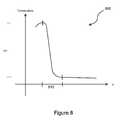
- FIG. 8is a simplified plot of temperature gradient in z direction in the seal region according to an embodiment of the present invention.
- the present inventionrelates generally to solar energy techniques.
- the present inventionprovides a method and resulting device fabricated from a plurality of concentrating elements respectively coupled to a plurality of photovoltaic regions.
- concentrating elementsare coupled to a plurality of photovoltaic regions using one or more coupled structures.
- the present method and structureare directed to a laser sealing technique of a solar cell package apparatus.
- the inventionhas been applied to solar panels, commonly termed modules, but it would be recognized that the invention has a much broader range of applicability.
- FIG. 1is a simplified diagram of a solar cell according to an embodiment of the present invention.
- This diagramis merely an example, which should not unduly limit the scope of the claims herein.
- One of ordinary skill in the artwould recognize other variations, modifications, and alternatives.
- the devicehas a back cover member 101 , which includes a surface area and a back area.
- the back cover memberalso has a plurality of sites, which are spatially disposed, for electrical members, such as bus bars, and a plurality of photovoltaic regions.
- the back covercan be free from any patterns and is merely provided for support and packaging.
- the devicehas a plurality of photovoltaic strips 105 , each of which is disposed overlying the surface area of the back cover member.
- the plurality of photovoltaic stripscorresponds to a cumulative area occupying a total photovoltaic spatial region, which is active and converts sunlight into electrical energy.
- An encapsulating material 115is overlying a portion of the back cover member. That is, an encapsulating material forms overlying the plurality of strips, and exposed regions of the back cover, and electrical members.
- the encapsulating materialcan be a single layer, multiple layers, or portions of layers, depending upon the application.
- the encapsulating materialcan be provided overlying a portion of the photovoltaic strips or a surface region of the front cover member, which would be coupled to the plurality of photovoltaic strips.
- a front cover member 121is coupled to the encapsulating material. That is, the front cover member is formed overlying the encapsulant to form a multilayered structure including at least the back cover, bus bars, plurality of photovoltaic strips, encapsulant, and front cover.
- the front coverincludes one or more concentrating elements, which concentrate (e.g., intensify per unit area) sunlight onto the plurality of photovoltaic strips. That is, each of the concentrating elements can be associated respectively with each of or at least one of the photovoltaic strips.
- an interface regionis provided along at least a peripheral region of the back cover member and the front cover member.
- the interface regionmay also be provided surrounding each of the strips or certain groups of the strips depending upon the embodiment.
- the devicehas a sealed region and is formed on at least the interface region to form an individual solar cell from the back cover member and the front cover member.
- the sealed regionmaintains the active regions, including photovoltaic strips, in a controlled environment free from external effects, such as weather, mechanical handling, environmental conditions, and other influences that may degrade the quality of the solar cell.
- the sealed region and/or sealed member(e.g., two substrates) protect certain optical characteristics associated with the solar cell and also protects and maintains any of the electrical conductive members, such as bus bars, interconnects, and the like.
- the sealed member structurethere can be other benefits achieved using the sealed member structure according to other embodiments.
- the total photovoltaic spatial regionoccupies a smaller spatial region than the surface area of the back cover. That is, the total photovoltaic spatial region uses less silicon than conventional solar cells for a given solar cell size. In a preferred embodiment, the total photovoltaic spatial region occupies about 80% and less of the surface area of the back cover for the individual solar cell. Depending upon the embodiment, the photovoltaic spatial region may also occupy about 70% and less or 60% and less or preferably 50% and less of the surface area of the back cover or given area of a solar cell. Of course, there can be other percentages that have not been expressly recited according to other embodiments.
- back cover memberand “front cover member” are provided for illustrative purposes, and not intended to limit the scope of the claims to a particular configuration relative to a spatial orientation according to a specific embodiment. Further details of each of the various elements in the solar cell can be found throughout the present specification and more particularly below.
- the present inventionprovides a packaged solar cell assembly being capable of stand-alone operation to generate power using the packaged solar cell assembly and/or with other solar cell assemblies.
- the packaged solar cell assemblyincludes rigid front cover member having a front cover surface area and a plurality of concentrating elements thereon.
- the rigid front cover memberconsists of a variety of materials.
- the rigid front coveris made of polymer material.
- the rigid front coveris made of transparent polymer material having a reflective index of about 1.4 or 1.42 or greater.
- the rigid front coverhas a Young's Modulus of a suitable range.
- Each of the concentrating elementshas a length extending from a first portion of the front cover surface area to a second portion of the front cover surface area.
- Each of the concentrating elementshas a width provided between the first portion and the second portion.
- Each of the concentrating elementshaving a first edge region coupled to a first side of the width and a second edge region provided on a second side of the width. The first edge region and the second edge region extend from the first portion of the front cover surface area to a second portion of the front cover surface area.
- the plurality of concentrating elementsis configured in a parallel manner extending from the first portion to the second portion.
- the embodimentmay further includes a first electrode member that is coupled to a first region of each of the plurality of photovoltaic strips and a second electrode member coupled to a second region of each of the plurality of photovoltaic strips.
- the solar cell assemblyadditionally includes a first electrode member coupled to a first region of each of the plurality of photovoltaic strips and a second electrode member coupled to a second region of each of the plurality of photovoltaic strips.
- the first electrodeincludes a first protruding portion extending from a first portion of the sandwiched assembly and the second electrode comprising a second protruding portion extending from a second portion of the sandwiched assembly.
- the present inventionprovides a solar cell apparatus.
- the solar cell apparatusincludes a backside substrate member comprising a backside surface region and an inner surface region.
- the backside substrate membercan be made from various materials.
- the backside memberis characterized by a polymer material.
- the present inventionprovides a solar cell apparatus that includes a backside substrate member.
- the backside substrate memberincludes a backside surface region and an inner surface region.
- the backside substrate memberis characterized by a width.
- the backside substrate memberis characterized by a length of about eight inches and less.
- the backside substrate memberis characterized by a width of about 8 inches and less and a length of more than 8 inches.
- there can be other variations, modifications, and alternatives. Further details of the solar cell assemblycan be found in U.S. patent application Ser. No. 11/445,993, commonly assigned, and hereby incorporated by reference herein.
- FIG. 2is a simplified diagram of solar cell concentrating elements 201 according to an embodiment of the present invention.
- This diagramis merely an example, which should not unduly limit the scope of the claims herein.
- One of ordinary skill in the artwould recognize other variations, modifications, and alternatives.
- each of the concentrating elements for the strip configurationincludes a trapezoidal shaped member 205 .
- Each of the trapezoidal shaped membershas a bottom surface 203 coupled to a pyramidal shaped region coupled to an upper region 207 .
- the upper regionis defined by surface 209 , which is co-extensive of the front cover.
- Each of the membersis spatially disposed and in parallel to each other according to a specific embodiment.
- the term “trapezoidal” or “pyramidal”may include embodiments with straight or curved or a combination of straight and curved walls according to embodiments of the present invention.
- the concentrating elementsmay be on the front cover, integrated into the front cover, and/or be coupled to the front cover according to embodiments of the present invention. Further details of the front cover with concentrating elements are provided more particularly below.
- a solar cell apparatusincludes a shaped concentrator device operably coupled to each of the plurality of photovoltaic strips.
- the shaped concentrator devicehas a first side and a second side.
- the solar cell apparatusincludes an aperture region provided on the first side of the shaped concentrator device.
- the concentrator deviceincludes a first side region and a second side region.
- the first side regionis characterized by a roughness of about 100 nanometers or 120 nanometers RMS and less
- the second side regionis characterized by a roughness of about 100 nanometers or 120 nanometers RMS and less.
- the roughnessis characterized by a dimension value of about 10% of a light wavelength derived from the aperture regions.
- the backside membercan have a pyramid-type shape.
- the solar cell apparatusincludes an exit region provided on the second side of the shaped concentrator device.
- the solar cell apparatusincludes a geometric concentration characteristic provided by a ratio of the aperture region to the exit region. The ratio can be characterized by a range from about 1.8 to about 4.5.
- the solar cell apparatusalso includes a polymer material characterizing the shaped concentrator device.
- the solar cell apparatusadditionally includes a refractive index of about 1.45 and greater characterizing the polymer material of the shaped concentrator device.
- the solar cell apparatusincludes a coupling material formed overlying each of the plurality of photovoltaic strips and coupling each of the plurality of photovoltaic regions to each of the concentrator devices.
- the coupling materialis characterized by a suitable Young's Modulus.
- the solar cell apparatusincludes a refractive index of about 1.45 and greater characterizing the coupling material coupling each of the plurality of photovoltaic regions to each of the concentrator device.
- the polymer materialis characterized by a thermal expansion constant that is suitable to withstand changes due to thermal expansion of elements of the solar cell apparatus.
- the plurality of concentrating elementshas a light entrance area (A 1 ) and a light exit area (A 2 ) such that A 2 /A 1 is 0.8 and less.
- the plurality of concentrating elementshas a light entrance area (A 1 ) and a light exit area (A 2 ) such that A 2 /A 1 is 0.8 and less, and the plurality of photovoltaic strips are coupled against the light exit area.
- the ratio of A 2 /A 1is about 0.5 and less.
- each of the concentrating elementshas a height of 7 mm or less.
- the sealed sandwiched assemblyhas a width ranging from about 100 millimeters to about 210 millimeters and a length ranging from about 100 millimeters to about 210 millimeters. In a specific embodiment, the sealed sandwiched assembly can even have a length of about 300 millimeters and greater.
- each of the concentrating elementshas a pair of sides. In a specific embodiment, each of the sides has a surface finish of 100 nanometers or less or 120 nanometers and less RMS. Of course, there can be other variations, modifications, and alternatives.
- FIG. 2Athe front cover has been illustrated using a side view 201 , which is similar to FIG. 2 .
- the front coveralso has a top-view illustration 210 .
- a section view 220 from “B-B”has also been illustrated.
- a detailed view “A” of at least two of the concentrating elements 230is also shown.
- the concentrating elementsare made of a suitable material.
- the concentrating elementscan be made of a polymer, glass, or other optically transparent materials, including any combination of these, and the like.
- the suitable materialis preferably environmentally stable and can withstand environmental temperatures, weather, and other “outdoor” conditions.
- the concentrating elementscan also include portions that are coated with an anti-reflective coating for improved efficiency. Coatings can also be used for improving a durability of the concentrating elements.
- the solar cell apparatusincludes a first reflective side provided between a first portion of the aperture region and a first portion of the exit region.
- the first reflective sideincludes a first polished surface of a portion of the polymer material.
- the first reflective sideis characterized by a surface roughness of about 120 nanometers RMS and less.
- the solar cell apparatusincludes a second reflective side provided between a second portion of the aperture region and a second portion of the exit region.
- the second reflective sidecomprises a second polished surface of a portion of the polymer material.
- the second reflective sideis characterized by a surface roughness of about 120 nanometers and less.
- the first reflective side and the second reflective sideprovide for total internal reflection of one or more photons provided from the aperture region.
- the solar cell apparatusincludes a geometric concentration characteristic provided by a ratio of the aperture region to the exit region. The ratio is characterized by a range from about 1.8 to about 4.5.
- the solar cell apparatusincludes a polymer material characterizing the shaped concentrator device, which includes the aperture region, exit region, first reflective side, and second reflective side. As an example, the polymer material is capable of being free from damaged caused by ultraviolet radiation.
- the solar cell apparatushas a refractive index of about 1.45 and greater characterizing the polymer material of the shaped concentrator device.
- the solar cell apparatusincludes a coupling material formed overlying each of the plurality of photovoltaic strips and coupling each of the plurality of photovoltaic regions to each of the concentrator devices.
- the solar cell apparatusadditionally includes one or more pocket regions facing each of the first reflective side and the second reflective side.
- the one or more pocket regionscan be characterized by a refractive index of about 1 to cause one or more photons from the aperture region to be reflected toward the exit region.
- each of the concentrating elementsis separated by a region having a notch structure of a predetermined size and shape according to a specific embodiment.
- notch structurescan be found throughout the present specification and more particularly below.
- FIG. 3is a simplified flow diagram illustrating a method of assembling a solar cell apparatus according to an embodiment of the present invention.
- the methodprovides a first substrate member (Step 302 ).
- the first substrate memberincludes a plurality of photovoltaic strips thereon.
- the methodprovides a second substrate member (Step 304 ) which includes a plurality of optical concentrating elements.
- the first substrate memberis aligned and couple to the second substrate member (Step 306 ).
- an inner region of the second substrate member(Step 308 ) is blocked from irradiation while a peripheral region remained exposed (Step 310 ).
- a pressureis applied (Step 314 ).
- the methodincludes irradiating the exposed peripheral region of the second substrate member (Step 312 ) and forming a melting region in an interface region between the first substrate member and the second substrate member. The melting region is used to seal peripheral interface between first substrate and second substrate (Step 316 ).
- the methodcontinues with other steps (Step 318 ) to complete the solar cell panel.
- FIG. 3Ais a simplified flow diagram illustrating a method of assembling a solar cell apparatus according to an embodiment of the present invention.
- the methodprovides a first substrate member (Step 302 ).
- the first substrate memberincludes a plurality of photovoltaic strips thereon.
- the methodprovides a second substrate member (Step 304 ) which includes a plurality of optical concentrating elements.
- the methodalso includes providing a high emissivity back cover device (Step 305 ).
- the first substrate memberis aligned and couple to the second substrate member (Step 306 ).
- an inner region of the second substrate member(Step 308 ) is blocked from irradiation while a peripheral region remained exposed (Step 310 ).
- a pressureis applied (Step 314 ).
- the methodincludes irradiating the exposed peripheral region of the second substrate member (Step 312 ) and forming a melting region in an interface region between the first substrate member and the second substrate member.
- laseris used for providing irradiation.
- the melting regionis used to seal peripheral interface between first substrate and second substrate (Step 316 ).
- the methodcontinues with other steps (Step 318 ) to complete the solar cell panel.
- FIG. 3Bis a simplified flow diagram illustrating a method of assembling a solar cell apparatus according to an embodiment of the present invention.
- the methodprovides a first substrate member (Step 302 ).
- the first substrate memberincludes a plurality of photovoltaic strips thereon.
- the methodprovides a second substrate member (Step 304 ) which includes a plurality of optical concentrating elements.
- the methodalso includes providing a high emissivity back cover device (Step 305 ).
- the first substrate memberis aligned and couple to the second substrate member (Step 306 ).
- a pressureis applied (Step 308 ).
- an inner region of the second substrate member(Step 310 ) is blocked from irradiation while a peripheral region remained exposed (Step 312 ).
- the methodincludes irradiating the exposed peripheral region of the second substrate member (Step 314 ) and forming a melting region in an interface region between the first substrate member and the second substrate member. The melting region is used to seal peripheral interface between first substrate and second substrate (Step 316 ). The method continues with other steps (Step 318 ) to complete the solar cell panel.
- FIG. 4is a simplified diagram of coupling 400 a back cover member 401 to a concentrator member 402 according to an embodiment of the present invention.
- This diagramis merely an example, which should not unduly limit the scope of the claims herein.
- the back cover member 401includes, a first peripheral region 404 , which has a protruding structure 406 and a first flat region in a portion of the first peripheral region.
- the concentrator memberincludes a second peripheral region 408 , which has an indent structure 410 and a second flat region in a portion of the second peripheral region.
- the protruding structure and the indent structureprovides a tongue and groove mechanism to couple the back cover member and the concentrator member. Additionally, the back cover member and the concentrator member may be aligned using the tongue and groove mechanism in a specific embodiment, the protruding structure 406 of the back cover member is aligned to a second peripheral region 408 of the concentrator member such that each of the plurality of photovoltaic strips is coupled to a concentrator element in the concentrator member. As shown in FIG. 4 , the coupled substrate member includes an interface region 412 formed from the first peripheral region and the second peripheral region. In a specific embodiment, the protruding structure 410 has a semi-circular cross section.
- the protruding structure 410has a diameter of about 10/1000 of an inch or less and runs along the second peripheral region of the concentrator member.
- the protruding structurecan be any shape, for example, the cross section can be rectangular, or other polygon shapes.
- the indent structurecan be shaped accordingly to mate with the protruding structure.
- the interface regionmay be subjected to a cleaning process to remove any material that may affect sealing of the substrate members.
- the cleaning processcan include using a suitable solvents or a combination of solvents followed by drying.
- the cleaning processmay include a plasma cleaning, or a blasting process to remove undesirable material.
- a plasma cleaningor a blasting process to remove undesirable material.
- a forceis provided to mechanically couple the aligned concentrator member to the back cover member.
- the forcemay be provided by a plate, fluid pressure, a clamp or any other suitable techniques. Further details of the applied force can be found through the present specification and particularly below. Of course there can be other variations, modifications, and alternatives.
- FIG. 5-7are simplified diagrams of joining the concentrator member and back cover member and to seal them together using an electromagnetic radiation according to an embodiment of the present invention. These diagrams are merely examples, which should not unduly limit the scope of the claims herein. One of ordinary skill in the art would recognize other variations, modifications, and alternatives.
- a stage member including a waveguide device 504is provided.
- the waveguide deviceincludes an inner waveguide 506 , an outer waveguide 508 , and an opening region 510 .
- the waveguide devicealso includes an upper surface region 512 and a back surface region 514 .
- the electromagnetic radiationis allowed to pass through the opening region of the waveguide device and blocked by the inner waveguide region and the outer waveguide region.
- the opening regionincludes a straight face region 518 and an oblique face region 520 .
- the straight face regionmay be a flat surface.
- the straight face regionmay also be a curved surface that is concave or convex depending on the application.
- the oblique face regionmay be a flat surface.
- the oblique face regionmay be a curved surface depending upon the application.
- the oblique face region and the straight face regionallow for a maximum transmission of the electromagnetic radiation through the opening region.
- the waveguide deviceis preferably made of a highly reflective material at least in the straight face region and the oblique face region.
- the waveguide deviceis made of a gold plated alloy.
- the alloymay be steel and/or other metal materials.
- the waveguide deviceis configured to allow for a concentration of the electromagnetic radiation to concentrate at a weld region 516 in the peripheral region in a specific embodiment. A top view of the waveguide device is shown in FIG. 5A . Of cause there can be other variations, modifications, and alternatives.
- the waveguide deviceis provided overlying the aperture region of the concentrator member.
- a force 522is applied on the front surface region of the waveguide device to mechanically couple the concentrator member to the back cover member to form the peripheral region as also shown in FIG. 5 .
- the mechanical forcecan be provided using air pressure or a weight such as a cylinder providing a pressure ranging from about 100 psi to about 200 psi. Other means of mechanical forces, such as an air pressure, may also be used. Of course there can be other variations, modifications, and alternatives.
- the coupled concentrator member and the back cover memberis irradiated using an electromagnetic radiation 602 .
- the electromagnetic radiationmay be provided using a energy source such as a laser source or a flash lamp or other suitable energy source.
- the electromagnetic radiationmay be provided using a laser (e.g., laser diode, tunable dye, etc.) having a suitable wavelength range and providing a suitable power range.
- the electromagnetic radiationis provided for a time period of about eight seconds or less and preferably 1-4 seconds. Effectively, the electromagnetic radiation traverses through the entire exposed peripheral region of at least the concentrator member of the coupled substrate within the entire time period and provides energy to cause a melt region 608 in the interface region while the inner region is blocked from the electromagnetic radiation.
- the electromagnetic radiation and/or laser energyis guided using one or more fiber optics 606 from a source 604 and through the opening region of the waveguide device to the peripheral region of the coupled substrate to provide energy to cause the melt region in the peripheral region.
- the source 604is a laser source.
- the laser sourceprovides pulses of energy and the one or more fiber optics are allowed to translate above the opening region of the waveguide device to provide energy to cause the melt region in the interface region of the coupled substrate members in a specific embodiment.
- the electromagnetic radiationcan be derived from Laser IRAM assembly systems Models 200 and 300 manufactured by Branson Ultrasonics Corp., 41 Eagle Rd., Danbury, Conn. 06813-1961, USA. Of course there can be other variations, modifications, and alternatives.
- the light/laser radiationtraverses through the entire thickness of the concentrator member, which can be a polymer component transmissive to light.
- the energyis absorbed at least by the back cover member at the interface region to cause a melt region 608 in the interface region.
- the back cover memberis made of a light absorbing material at least in the second peripheral region.
- the light absorbing materialabsorbs irradiation energy traversing at least the first peripheral region of the concentrator element, which is transparent, to cause heating and to form the melting region in the interface region.
- the light absorbing materialcan also be a light blocking material or include each of these characteristics.
- the light absorbing materialmay be provided in the interface region to absorb the irradiation energy to cause heating and forming the melt region in the interface region.
- the concentrator elementcan be made of an acrylic material characterized by a high transmisivity to light.
- the back cover membercan be a polymer having a high emmisivity.
- the back cover membercan be an acrylic material.
- the back cover membercan be a polycarbonate material.
- the irradiation energyheats the interface region to a temperature of about 110 Degree Celsius to about 115 Degree Celsius to cause the melt region configured to be light absorbing.
- E Branges from 90% to 95% of E, that is 90% to 95% of the energy is transmitted through the concentrator member and absorbed by the back cover member to cause the melt region in the peripheral region.
- the melt regionforms a seal region 702 for the back cover member and the concentrator member.
- FIG. 7is a simplified side-view diagram of a concentrator member and a back cover member according to an embodiment of the present invention. This diagram is merely an example, which should not unduly limit the scope of the claims herein. One of ordinary skill in the art would recognize other variations, modifications, and alternatives.
- the melt regionforms a seal region 702 for the back cover member and the concentrator member. A more detailed diagram of the seal region is also shown.
- the seal regionhas a width 704 of about 50 um or less and can include a protruded region 706 .
- the seal region providedis free of contaminations such as particulates or chemical species as may occur by other means.
- the seal regionmaintains the photovoltaic strips and electrical conducting element in a desired controlled environment and provides protection from elements such as moisture and others.
- the irradiation energycauses a temperature gradient within the interface region.
- acrylicas the material for the concentrator member and polycarbonate as the material for the back cover member as an example.
- the polycarbonateis designed to be light absorbing and the acrylic is designed to be transmissive.
- the energy transmitted through the first peripheral region of the concentrator memberprovides heat energy to increase the temperature of the interface region to about 105 Degree Celsius to about 120 Degree Celsius to cause the melt region.
- the temperature gradientis provided within a vertical distance in the interface region as illustrated in a simplified plot 800 in FIG. 8 . As shown, the temperature is provided on vertical axis and the vertical distance is provided on the horizontal axis. The temperature gradient is essentially provided within a vertical distance 701 as shown.
- the temperature gradientis provided within a vertical distance of about 40 micron to about 50 micron in the vertical direction. That is the thermal energy is provided within vertical distance 801 for a time period to form the melt region in a specific embodiment.
- the time periodis about eight seconds or less and preferably 4-6 seconds in a specific embodiment.
Landscapes
- Engineering & Computer Science (AREA)
- Mechanical Engineering (AREA)
- Physics & Mathematics (AREA)
- Optics & Photonics (AREA)
- Health & Medical Sciences (AREA)
- Electromagnetism (AREA)
- Toxicology (AREA)
- Thermal Sciences (AREA)
- Plasma & Fusion (AREA)
- Photovoltaic Devices (AREA)
Abstract
Description
E=EC+EB.
- where E is the energy provided by the electromagnetic radiation,
- ECis the energy absorbed by the concentrator member in the peripheral region, and
- EBis the energy absorbed by the back cover member in the peripheral region.
Claims (25)
Priority Applications (2)
| Application Number | Priority Date | Filing Date | Title |
|---|---|---|---|
| US12/060,801US7910392B2 (en) | 2007-04-02 | 2008-04-01 | Method and system for assembling a solar cell package |
| PCT/US2008/059167WO2008122046A2 (en) | 2007-04-02 | 2008-04-02 | Method and system for assembling a solar cell package |
Applications Claiming Priority (3)
| Application Number | Priority Date | Filing Date | Title |
|---|---|---|---|
| US90969207P | 2007-04-02 | 2007-04-02 | |
| US90969107P | 2007-04-02 | 2007-04-02 | |
| US12/060,801US7910392B2 (en) | 2007-04-02 | 2008-04-01 | Method and system for assembling a solar cell package |
Publications (2)
| Publication Number | Publication Date |
|---|---|
| US20080236664A1 US20080236664A1 (en) | 2008-10-02 |
| US7910392B2true US7910392B2 (en) | 2011-03-22 |
Family
ID=39792208
Family Applications (1)
| Application Number | Title | Priority Date | Filing Date |
|---|---|---|---|
| US12/060,801Expired - Fee RelatedUS7910392B2 (en) | 2007-04-02 | 2008-04-01 | Method and system for assembling a solar cell package |
Country Status (2)
| Country | Link |
|---|---|
| US (1) | US7910392B2 (en) |
| WO (1) | WO2008122046A2 (en) |
Cited By (1)
| Publication number | Priority date | Publication date | Assignee | Title |
|---|---|---|---|---|
| US20100173441A1 (en)* | 2007-02-15 | 2010-07-08 | Transform Solar Pty Ltd | Method for processing elongate substrates and substrate securing apparatus |
Families Citing this family (12)
| Publication number | Priority date | Publication date | Assignee | Title |
|---|---|---|---|---|
| US8227688B1 (en) | 2005-10-17 | 2012-07-24 | Solaria Corporation | Method and resulting structure for assembling photovoltaic regions onto lead frame members for integration on concentrating elements for solar cells |
| US7910822B1 (en) | 2005-10-17 | 2011-03-22 | Solaria Corporation | Fabrication process for photovoltaic cell |
| US7910392B2 (en) | 2007-04-02 | 2011-03-22 | Solaria Corporation | Method and system for assembling a solar cell package |
| US20090056806A1 (en)* | 2007-09-05 | 2009-03-05 | Solaria Corporation | Solar cell structure including a plurality of concentrator elements with a notch design and predetermined radii and method |
| US8119902B2 (en) | 2007-05-21 | 2012-02-21 | Solaria Corporation | Concentrating module and method of manufacture for photovoltaic strips |
| US7910035B2 (en) | 2007-12-12 | 2011-03-22 | Solaria Corporation | Method and system for manufacturing integrated molded concentrator photovoltaic device |
| US20100294338A1 (en)* | 2009-02-20 | 2010-11-25 | Solaria Corporation | Large Area Concentrator Lens Structure and Method |
| US20120024353A1 (en)* | 2009-03-03 | 2012-02-02 | Arkema France | Thermoformable photovoltaic backsheet |
| WO2012135333A1 (en)* | 2011-03-31 | 2012-10-04 | Dow Corning Corporation | Method of forming a photovoltaic cell module with a cell press |
| USD699176S1 (en) | 2011-06-02 | 2014-02-11 | Solaria Corporation | Fastener for solar modules |
| KR101791130B1 (en)* | 2016-11-18 | 2017-10-27 | 엘지전자 주식회사 | Solar cell module |
| CN111091444B (en)* | 2019-11-28 | 2023-09-26 | 西安隆基智能技术有限公司 | Solar cell matching method and device and electronic equipment |
Citations (244)
| Publication number | Priority date | Publication date | Assignee | Title |
|---|---|---|---|---|
| US2470618A (en) | 1946-03-26 | 1949-05-17 | Lawrence T Holden | Electrical apparatus |
| US3330700A (en) | 1963-06-17 | 1967-07-11 | Electro Optical Systems Inc | Solar-cell panels |
| US3446676A (en) | 1966-09-07 | 1969-05-27 | Webb James E | Solar battery with interconnecting means for plural cells |
| GB1187969A (en) | 1966-11-24 | 1970-04-15 | Pilkington Brothers Ltd | Improvements relating to the Manufacture of Glass in Sheet Form. |
| US3575721A (en) | 1965-04-26 | 1971-04-20 | Textron Inc | Solar cell arrays and connectors |
| US3597050A (en) | 1966-12-30 | 1971-08-03 | Glaverbel | Transparent article having modified radiation-transmitting properties |
| US3641354A (en) | 1967-03-08 | 1972-02-08 | Jack De Ment | Optical modulation by fluidic optics utilizing chromatic aberration |
| US3700714A (en) | 1971-06-24 | 1972-10-24 | Stephen B Hamilton | Curable compositions |
| US3819417A (en) | 1972-05-17 | 1974-06-25 | Communications Satellite Corp | Mechanically interlaced and electrically interconnected silicon solar cells |
| US3849880A (en) | 1969-12-12 | 1974-11-26 | Communications Satellite Corp | Solar cell array |
| US3951633A (en) | 1974-12-23 | 1976-04-20 | Combustion Engineering, Inc. | Method for producing patterned glass on a float ribbon |
| US3993505A (en) | 1975-05-27 | 1976-11-23 | Hughes Aircraft Company | Interconnector for components such as solar cells or the like |
| US3999283A (en) | 1975-06-11 | 1976-12-28 | Rca Corporation | Method of fabricating a photovoltaic device |
| US4029519A (en) | 1976-03-19 | 1977-06-14 | The United States Of America As Represented By The United States Energy Research And Development Administration | Solar collector having a solid transmission medium |
| US4056405A (en) | 1976-05-10 | 1977-11-01 | Solarex Corporation | Panel for solar energy cells |
| US4091798A (en) | 1977-02-03 | 1978-05-30 | Nasa | Non-tracking solar energy collector system |
| US4097308A (en) | 1977-04-28 | 1978-06-27 | Tideland Signal Corporation | Glass enclosed solar cell panel |
| US4106952A (en) | 1977-09-09 | 1978-08-15 | Kravitz Jerome H | Solar panel unit |
| US4118249A (en) | 1977-08-30 | 1978-10-03 | The United States Of America As Represented By The United States Department Of Energy | Modular assembly of a photovoltaic solar energy receiver |
| US4143234A (en) | 1976-11-08 | 1979-03-06 | Monsanto Company | Solar collector using total internal reflectance |
| US4166917A (en) | 1978-05-22 | 1979-09-04 | Corning Glass Works | Concentrating solar receiver |
| US4170507A (en) | 1977-12-27 | 1979-10-09 | Motorola, Inc. | Method for encapsulating a solar cell array |
| US4174978A (en) | 1978-05-11 | 1979-11-20 | Chubrikov Boris A | Semiconductor photovoltaic generator and method of fabricating thereof |
| US4193820A (en) | 1977-10-07 | 1980-03-18 | Organisation Europeenne De Recherches Spatiales | Interconnection device for solar cells |
| US4203646A (en) | 1978-05-17 | 1980-05-20 | Amp Incorporated | Clip for electrically connecting planar elements, such as solar cells, and the like, in series |
| US4239555A (en) | 1979-07-30 | 1980-12-16 | Mobil Tyco Solar Energy Corporation | Encapsulated solar cell array |
| US4257821A (en) | 1978-11-13 | 1981-03-24 | Trw Inc. | Universal solar cell/conductor junction element and solar panel embodying same |
| US4291191A (en) | 1979-07-03 | 1981-09-22 | Licentia Patent-Verwaltungs G.M.B.H. | Solar cell arrangement |
| US4293192A (en) | 1980-05-27 | 1981-10-06 | Bronstein Allen I | Solar reflector with flexible sheet tightly secured around form surfaces |
| US4295463A (en) | 1976-04-26 | 1981-10-20 | Citron Jeffrey M | Flexible V-shaped solar tracking concentrating solar energy collector |
| US4333447A (en) | 1980-06-04 | 1982-06-08 | Corning Glass Works | Solar receiver tube support |
| US4355478A (en)* | 1980-06-19 | 1982-10-26 | Armstrong Joe W | Method for making framed structures |
| US4361136A (en) | 1980-08-26 | 1982-11-30 | Linus Huang | Concentric solar collector |
| US4362903A (en) | 1980-12-29 | 1982-12-07 | General Electric Company | Electrical conductor interconnect providing solderable connections to hard-to-contact substrates, such as liquid crystal cells |
| US4404422A (en) | 1980-09-26 | 1983-09-13 | Unisearch Limited | High efficiency solar cell structure |
| US4440153A (en) | 1981-03-02 | 1984-04-03 | Imchemie Kunststoff Gmbh | Solar concentrator |
| US4449514A (en) | 1982-06-25 | 1984-05-22 | The United States Of America As Represented By The Administrator Of The National Aeronautics And Space Administration | Solar concentrator protective system |
| US4454371A (en) | 1981-12-03 | 1984-06-12 | The United States Of America As Represented By The Secretary Of The Air Force | Solar energy concentrator system |
| US4457297A (en) | 1982-03-08 | 1984-07-03 | Ford Aerospace & Communications Corp. | Modular solar concentrator |
| EP0029721B1 (en) | 1979-11-26 | 1984-07-25 | Exxon Research And Engineering Company | Solar cell modules |
| US4463749A (en) | 1982-03-08 | 1984-08-07 | Ford Aerospace & Communications Corporation | Modular solar concentrator |
| US4495360A (en) | 1982-04-30 | 1985-01-22 | General Electric Company | Ultraviolet light absorbing agents, method for making, compositions and articles containing same |
| US4511618A (en) | 1981-04-24 | 1985-04-16 | Glaverbel | Laminated reflective panels |
| US4562637A (en)* | 1983-06-22 | 1986-01-07 | Hitachi, Ltd. | Method of manufacturing solar battery |
| US4571812A (en) | 1984-02-16 | 1986-02-25 | Industrial Solar Technology | Method for making a solar concentrator and product |
| JPS6144741A (en) | 1984-08-10 | 1986-03-04 | Bridgestone Corp | Production of laminate |
| US4589191A (en) | 1983-10-20 | 1986-05-20 | Unisearch Limited | Manufacture of high efficiency solar cells |
| US4638110A (en) | 1985-06-13 | 1987-01-20 | Illuminated Data, Inc. | Methods and apparatus relating to photovoltaic semiconductor devices |
| US4663562A (en) | 1984-07-16 | 1987-05-05 | General Electric Company | Contrast enhancement structure for color cathode ray tube |
| US4668314A (en) | 1983-10-25 | 1987-05-26 | Casio Computer Co., Ltd. | Method of manufacturing a small electronic device |
| US4680074A (en) | 1984-05-16 | 1987-07-14 | Licentia Patent-Verwaltungs-Gmbh | Method for producing a carrier material for the solar cells of a solar generator |
| US4683154A (en) | 1985-08-19 | 1987-07-28 | The United States Of America As Represented By The United States Department Of Energy | Laser sealed vacuum insulation window |
| US4692557A (en) | 1986-10-16 | 1987-09-08 | Shell Oil Company | Encapsulated solar cell assemblage and method of making |
| US4691994A (en) | 1981-10-06 | 1987-09-08 | Afian Viktor V | Method for a solar concentrator manufacturing |
| US4697042A (en) | 1985-07-27 | 1987-09-29 | Telefunken Electronic Gmbh | Solar generator |
| US4711972A (en) | 1985-07-05 | 1987-12-08 | Entech, Inc. | Photovoltaic cell cover for use with a primary optical concentrator in a solar energy collector |
| US4830038A (en) | 1988-01-20 | 1989-05-16 | Atlantic Richfield Company | Photovoltaic module |
| US4848319A (en) | 1985-09-09 | 1989-07-18 | Minnesota Mining And Manufacturing Company | Refracting solar energy concentrator and thin flexible Fresnel lens |
| US4863224A (en) | 1981-10-06 | 1989-09-05 | Afian Viktor V | Solar concentrator and manufacturing method therefor |
| US4953577A (en) | 1989-07-06 | 1990-09-04 | Solarex Corporation | Spray encapsulation of photovoltaic modules |
| US4964713A (en) | 1987-12-08 | 1990-10-23 | Fraunhofer-Gesellschaft zur Forderund der Forschung E. V. | Concentrator arrangement |
| US4999059A (en) | 1989-08-11 | 1991-03-12 | Bagno Robert G | Universal solar concentrator panel |
| US5006179A (en) | 1989-05-24 | 1991-04-09 | Solarex Corporation | Interconnect for electrically connecting solar cells |
| US5011544A (en) | 1989-09-08 | 1991-04-30 | Solarex Corporation | Solar panel with interconnects and masking structure, and method |
| US5043198A (en) | 1988-04-18 | 1991-08-27 | Somar Corporation | Lightsafe masking film |
| WO1991018420A1 (en) | 1990-05-21 | 1991-11-28 | The Boeing Company | Panel for solar concentrators and tandem cell units |
| US5080725A (en) | 1987-12-17 | 1992-01-14 | Unisearch Limited | Optical properties of solar cells using tilted geometrical features |
| US5118361A (en) | 1990-05-21 | 1992-06-02 | The Boeing Company | Terrestrial concentrator solar cell module |
| US5153780A (en) | 1991-06-10 | 1992-10-06 | The United States Of America As Represented By The United States Department Of Energy | Method and apparatus for uniformly concentrating solar flux for photovoltaic applications |
| US5158618A (en) | 1990-02-09 | 1992-10-27 | Biophotonics, Inc. | Photovoltaic cells for converting light energy to electric energy and photoelectric battery |
| US5167724A (en) | 1991-05-16 | 1992-12-01 | The United States Of America As Represented By The United States Department Of Energy | Planar photovoltaic solar concentrator module |
| US5174275A (en) | 1991-11-21 | 1992-12-29 | Holland Beecher J | Wide-angle solar concentrator |
| US5180442A (en) | 1992-04-06 | 1993-01-19 | Eric Elias | Integration system for solar modules |
| US5180888A (en) | 1989-08-10 | 1993-01-19 | Casio Computer Co., Ltd. | Conductive bonding agent and a conductive connecting method |
| US5224978A (en) | 1990-12-21 | 1993-07-06 | Saint-Gobain Vitrage International | Method for making hot rolled diffusing glazings |
| US5240510A (en) | 1991-09-23 | 1993-08-31 | Development Products Inc. | Photovoltaic cell |
| US5245985A (en) | 1991-01-16 | 1993-09-21 | Holland Beecher J | Effective and simple solar concentrator |
| US5261970A (en) | 1992-04-08 | 1993-11-16 | Sverdrup Technology, Inc. | Optoelectronic and photovoltaic devices with low-reflectance surfaces |
| WO1994006046A1 (en) | 1992-09-04 | 1994-03-17 | The Australian National University | Optical reflector arrays and apparatus using such arrays |
| US5344496A (en) | 1992-11-16 | 1994-09-06 | General Dynamics Corporation, Space Systems Division | Lightweight solar concentrator cell array |
| US5356488A (en) | 1991-12-27 | 1994-10-18 | Rudolf Hezel | Solar cell and method for its manufacture |
| US5365920A (en) | 1989-03-01 | 1994-11-22 | Bomin Solar Gmbh & Co. Kg | Solar concentrator system |
| WO1995006330A1 (en) | 1993-08-20 | 1995-03-02 | Kinkaid Christopher P | Non-tracking solar concentrator heat sink and housing system |
| US5395070A (en) | 1993-11-30 | 1995-03-07 | Stirbl; Robert C. | Solar energy concentrator assembly and associated method |
| US5409520A (en) | 1992-11-25 | 1995-04-25 | Mitsui Kinzoku Kogyo Kabushiki Kaisha | Copper powder for solderable and electroconductive paints and process for producing the same |
| US5436725A (en) | 1993-10-12 | 1995-07-25 | Hughes Aircraft Company | Cofocal optical system for thickness measurements of patterned wafers |
| US5460659A (en) | 1993-12-10 | 1995-10-24 | Spectrolab, Inc. | Concentrating photovoltaic module and fabrication method |
| US5466301A (en) | 1994-06-29 | 1995-11-14 | Texas Instruments Incorporated | Solar cell having an output-increasing, protective cover |
| US5468304A (en) | 1994-03-14 | 1995-11-21 | Texas Instruments Incorporated | Output-increasing, protective cover for a solar cell |
| WO1995033220A1 (en) | 1994-05-31 | 1995-12-07 | The Australian National University | Lenses formed by arrays of reflectors |
| US5478402A (en)* | 1994-02-17 | 1995-12-26 | Ase Americas, Inc. | Solar cell modules and method of making same |
| US5498297A (en) | 1994-09-15 | 1996-03-12 | Entech, Inc. | Photovoltaic receiver |
| US5508205A (en) | 1994-03-29 | 1996-04-16 | Amoco/Enron Solar | Method of making and utilizing partially cured photovoltaic assemblies |
| US5517339A (en) | 1994-06-17 | 1996-05-14 | Northeast Photosciences | Method of manufacturing high efficiency, broad bandwidth, volume holographic elements and solar concentrators for use therewith |
| US5529054A (en) | 1994-06-20 | 1996-06-25 | Shoen; Neil C. | Solar energy concentrator and collector system and associated method |
| WO1996023115A1 (en) | 1995-01-26 | 1996-08-01 | Myles John F Iii | A roof module having an integral solar energy concentrator |
| US5542409A (en) | 1995-01-06 | 1996-08-06 | Sampayo; Eduardo A. | Solar concentrator system |
| WO1996024954A1 (en) | 1995-02-09 | 1996-08-15 | Solardyne Corporation | Non-tracking solar concentrator heat sink and housing system |
| US5564411A (en) | 1995-01-26 | 1996-10-15 | Myles, Iii; John F. | Roof module having an integral solar energy concentrator |
| US5616186A (en) | 1995-09-18 | 1997-04-01 | Jx Crystals Inc. | Thermophotovoltaic electric generator using low bandgap photovoltaic cells with a hydrocarbon burner and enhanced catalytic infrared emitter |
| US5660644A (en) | 1995-06-19 | 1997-08-26 | Rockwell International Corporation | Photovoltaic concentrator system |
| US5665607A (en) | 1993-06-11 | 1997-09-09 | Mitsubishi Denki Kabushiki Kaisha | Method for producing thin film solar cell |
| US5707459A (en) | 1993-06-24 | 1998-01-13 | Canon Kabushiki Kaisha | Solar cell module provided with a heat-fused portion |
| US5709833A (en) | 1994-06-22 | 1998-01-20 | Husky Injection Molding Systems Ltd. | Pivoting workpiece removal method |
| WO1998003823A1 (en) | 1996-07-22 | 1998-01-29 | Stirling Thermal Motors, Inc. | Solar energy diffuser |
| US5735966A (en) | 1995-05-15 | 1998-04-07 | Luch; Daniel | Substrate structures for integrated series connected photovoltaic arrays and process of manufacture of such arrays |
| US5782993A (en) | 1996-06-28 | 1998-07-21 | Ponewash; Jackie | Photovoltaic cells having micro-embossed optical enhancing structures |
| WO1998032164A1 (en) | 1997-01-21 | 1998-07-23 | Boral Energy Limited | A method of producing thin silicon films |
| US5787878A (en) | 1996-09-23 | 1998-08-04 | Ratliff, Jr.; George D. | Solar concentrator |
| US5790304A (en) | 1993-05-10 | 1998-08-04 | Optical Coating Laboratory, Inc. | Self-healing UV-barrier coating for flexible polymer substrate |
| US5840147A (en) | 1995-06-07 | 1998-11-24 | Edison Welding Institute | Plastic joining method |
| US5846444A (en) | 1995-10-03 | 1998-12-08 | Corning Incorporated | Surface treatment of glass |
| US5851309A (en) | 1996-04-26 | 1998-12-22 | Kousa; Paavo | Directing and concentrating solar energy collectors |
| US5865905A (en) | 1996-09-30 | 1999-02-02 | Boeing North American, Inc. | Rolled film solar concentrator |
| WO1999005462A1 (en) | 1997-07-25 | 1999-02-04 | Arch Development Corporation | Nontracking solar concentrators |
| US5877874A (en) | 1995-08-24 | 1999-03-02 | Terrasun L.L.C. | Device for concentrating optical radiation |
| US5882434A (en) | 1996-10-15 | 1999-03-16 | United Solar Technologies, Inc. | Solar concentrator having an offset parabolic configuration |
| DE29823351U1 (en) | 1998-03-10 | 1999-05-06 | Vegla Vereinigte Glaswerke Gmbh, 52066 Aachen | Glazing to control the transmission of light |
| US5915170A (en) | 1994-09-20 | 1999-06-22 | Tessera, Inc. | Multiple part compliant interface for packaging of a semiconductor chip and method therefor |
| US5919316A (en) | 1997-06-27 | 1999-07-06 | The United States Of America As Represented By The Secretary Of The Air Force | Spacecraft solar array design to control differential charging |
| US5936777A (en) | 1996-10-31 | 1999-08-10 | Lightpath Technologies, Inc. | Axially-graded index-based couplers for solar concentrators |
| US5959787A (en) | 1995-06-06 | 1999-09-28 | The Boeing Company | Concentrating coverglass for photovoltaic cells |
| US5964216A (en) | 1997-10-10 | 1999-10-12 | Deutsches Zentrum Fuer Luft- Und Raumfahrt E.V. | Trough-type parabolic concentrator |
| US6008449A (en) | 1997-08-19 | 1999-12-28 | Cole; Eric D. | Reflective concentrating solar cell assembly |
| US6020553A (en) | 1994-10-09 | 2000-02-01 | Yeda Research And Development Co., Ltd. | Photovoltaic cell system and an optical structure therefor |
| US6034322A (en) | 1999-07-01 | 2000-03-07 | Space Systems/Loral, Inc. | Solar cell assembly |
| US6049035A (en) | 1997-09-18 | 2000-04-11 | Sanyo Electric Co., Ltd. | Photovoltaic device |
| US6057505A (en) | 1997-11-21 | 2000-05-02 | Ortabasi; Ugur | Space concentrator for advanced solar cells |
| US6074614A (en) | 1995-06-07 | 2000-06-13 | Molecular Devices Corporation | Multi-assay plate cover for elimination of meniscus |
| US6084175A (en) | 1993-05-20 | 2000-07-04 | Amoco/Enron Solar | Front contact trenches for polycrystalline photovoltaic devices and semi-conductor devices with buried contacts |
| US6091017A (en) | 1999-08-23 | 2000-07-18 | Composite Optics Incorporated | Solar concentrator array |
| US6093757A (en) | 1995-12-19 | 2000-07-25 | Midwest Research Institute | Composition and method for encapsulating photovoltaic devices |
| US6092392A (en) | 1997-04-30 | 2000-07-25 | Agfa-Gevaert, N.V. | Process for producing thin glass on roll |
| US6107564A (en) | 1997-11-18 | 2000-08-22 | Deposition Sciences, Inc. | Solar cell cover and coating |
| EP1030376A1 (en) | 1999-02-18 | 2000-08-23 | Sharp Kabushiki Kaisha | Solar cell module and solar cell panel |
| US6118067A (en) | 1998-11-20 | 2000-09-12 | Swales Aerospace | Method and apparatus for improved solar concentration arrays |
| US6134784A (en) | 1999-08-27 | 2000-10-24 | Photovoltaics International, Llc | Method of making solar collectors by in-situ encapsulation of solar cells |
| US6150602A (en) | 1999-05-25 | 2000-11-21 | Hughes Electronics Corporation | Large area solar cell extended life interconnect |
| WO2000074147A1 (en) | 1999-05-28 | 2000-12-07 | Terrasun, Llc | Device for concentrating optical radiation |
| WO2000079593A1 (en) | 1999-06-21 | 2000-12-28 | Aec-Able Engineering Co., Inc. | Solar cell array |
| US6167724B1 (en) | 1998-05-15 | 2001-01-02 | The Boc Group Plc | Pump |
| US6242685B1 (en) | 1999-03-25 | 2001-06-05 | Kaneka Corporation | Structure and method of installing photovoltaic module |
| WO2001051962A2 (en) | 2000-01-07 | 2001-07-19 | Midwest Research Institute | Multi-facet concentrator of solar setup for irradiating the objects placed in a target plane with solar light |
| US6264510B1 (en) | 1997-05-28 | 2001-07-24 | Harness System Technologies Research Ltd. | Laser-welded bus bar structure |
| US6274402B1 (en) | 1999-12-30 | 2001-08-14 | Sunpower Corporation | Method of fabricating a silicon solar cell |
| US6293803B1 (en) | 2000-02-09 | 2001-09-25 | Trw Inc. | Zee electrical interconnect |
| US6294723B2 (en) | 1998-02-26 | 2001-09-25 | Hitachi, Ltd. | Photovoltaic device, photovoltaic module and establishing method of photovoltaic system |
| US6309901B1 (en) | 1997-10-24 | 2001-10-30 | Agfa-Gevaert | Use of glass laminate as a substrate in semiconductor devices |
| US6315575B1 (en) | 1999-03-10 | 2001-11-13 | Sharp Kabushiki Kaisha | Interconnector electrically connecting plurality of electronic device elements, fabrication method thereof, and join apparatus thereof |
| US6320116B1 (en) | 1997-09-26 | 2001-11-20 | Evergreen Solar, Inc. | Methods for improving polymeric materials for use in solar cell applications |
| US6323415B1 (en) | 1998-09-18 | 2001-11-27 | Hitachi, Ltd. | Light concentrator photovoltaic module method of manufacturing same and light concentrator photovoltaic system |
| US6333458B1 (en) | 1999-11-26 | 2001-12-25 | The Trustees Of Princeton University | Highly efficient multiple reflection photosensitive optoelectronic device with optical concentrator |
| US6333457B1 (en) | 2000-08-29 | 2001-12-25 | Sunpower Corporation | Edge passivated silicon solar/photo cell and method of manufacture |
| US6337283B1 (en) | 1999-12-30 | 2002-01-08 | Sunpower Corporation | Method of fabricating a silicon solar cell |
| EP1174342A1 (en) | 2000-07-20 | 2002-01-23 | Université de Liège | Solar concentrator |
| WO2001055650A3 (en) | 2000-01-20 | 2002-02-21 | Bd Systems Llc | Self tracking, wide angle, solar concentrators |
| US6359209B1 (en) | 2000-02-23 | 2002-03-19 | Hughes Electronics Corporation | Solar panel and solar cell having in-plane solar cell interconnect with integrated diode tab |
| US6365823B1 (en) | 1997-06-20 | 2002-04-02 | Kaneka Corporation | Solar cell module and manufacturing method thereof |
| US6387726B1 (en) | 1999-12-30 | 2002-05-14 | Sunpower Corporation | Method of fabricating a silicon solar cell |
| US6395972B1 (en) | 2000-11-09 | 2002-05-28 | Trw Inc. | Method of solar cell external interconnection and solar cell panel made thereby |
| WO2001090661A3 (en) | 2000-05-24 | 2002-05-30 | Scott Frazier | Double reflecting solar concentrator |
| WO2002045143A1 (en) | 2000-11-29 | 2002-06-06 | Origin Energy Retail Limited | Semiconductor wafer processing to increase the usable planar surface area |
| US20020075579A1 (en) | 2000-12-18 | 2002-06-20 | Vasylyev Sergiy Victorovich | Apparatus for collecting and converting radiant energy |
| US6423568B1 (en) | 1999-12-30 | 2002-07-23 | Sunpower Corporation | Method of fabricating a silicon solar cell |
| US6429037B1 (en) | 1998-06-29 | 2002-08-06 | Unisearch Limited | Self aligning method for forming a selective emitter and metallization in a solar cell |
| US6433913B1 (en) | 1996-03-15 | 2002-08-13 | Gentex Corporation | Electro-optic device incorporating a discrete photovoltaic device and method and apparatus for making same |
| US6437236B2 (en) | 2000-01-24 | 2002-08-20 | Sumitomo Wiring Systems, Ltd. | Solar cell panel |
| US6440769B2 (en) | 1999-11-26 | 2002-08-27 | The Trustees Of Princeton University | Photovoltaic device with optical concentrator and method of making the same |
| US6441297B1 (en) | 1998-03-13 | 2002-08-27 | Steffen Keller | Solar cell arrangement |
| WO2002075225A2 (en) | 2001-03-16 | 2002-09-26 | Duke Solar Energy, Llc | Nonimaging solar concentrator with uniform irradiance |
| US20020139414A1 (en) | 2001-03-30 | 2002-10-03 | Vasylyev Sergiy Victorovich | Non-imaging system for radiant energy flux transformation |
| US6479744B1 (en) | 1997-12-22 | 2002-11-12 | Canon Kabushiki Kaisha | Photovoltaic device module |
| EP1261039A1 (en) | 2001-05-23 | 2002-11-27 | Université de Liège | Solar concentrator |
| US20030016539A1 (en) | 2000-03-16 | 2003-01-23 | Minano Juan C. | High efficiency non-imaging optics |
| US20030021897A1 (en) | 2001-07-12 | 2003-01-30 | Matsushita Electric Industrial Co., Ltd. | Screen printing apparatus and method of screen printing |
| US20030037814A1 (en) | 2001-08-24 | 2003-02-27 | Cohen Gilbert E. | Multiple reflector solar concentrators and systems |
| US20030037569A1 (en) | 2001-03-20 | 2003-02-27 | Mehran Arbab | Method and apparatus for forming patterned and/or textured glass and glass articles formed thereby |
| US6528718B2 (en) | 2000-09-11 | 2003-03-04 | Sharp Kabushiki Kaisha | Solar battery module |
| EP1131586B1 (en) | 1998-11-11 | 2003-03-19 | Phos Energy Inc. | Solar energy concentrator and converter |
| WO2003022578A1 (en) | 2001-09-11 | 2003-03-20 | The Australian National University | Solar energy concentrating assembly and sub-components thereof |
| US20030074976A1 (en) | 2001-09-04 | 2003-04-24 | Jalees Ahmad | Method and system for determining crack nucleation of a part subject to fretting fatigue |
| US20030081333A1 (en) | 1997-07-25 | 2003-05-01 | Roland Winston | Performance improvements of symmetry-breaking reflector structures in nonimaging devices |
| US20030095340A1 (en) | 2001-10-09 | 2003-05-22 | Atwater Harry A. | Nonimaging concentrator lens arrays and microfabrication of the same |
| WO2003047004A1 (en) | 2001-11-29 | 2003-06-05 | Origin Energy Solar Pty Ltd | Semiconductor texturing process |
| WO2003049201A1 (en) | 2001-12-04 | 2003-06-12 | Origin Energy Solar Pty Ltd | Method of making thin silicon sheets for solar cells |
| US20030121542A1 (en) | 2000-03-30 | 2003-07-03 | Wolfgang Harneit | Method for producing a solar module with thin-film solar cells which are series-connected in an integrated manner and solar modules produced according to the method, especially using concentrator modules |
| US20030156337A1 (en) | 2002-02-19 | 2003-08-21 | Mark Davidson | Mini-optics solar energy concentrator |
| US6609836B1 (en) | 2002-09-17 | 2003-08-26 | The United States Of America As Represented By The Secretary Of The Navy | Method for coupling fiber optic elements |
| US6617505B2 (en) | 2000-11-21 | 2003-09-09 | Sharp Kabushiki Kaisha | Solar battery module, replacement solar cell, and method of replacing solar cell |
| US6619282B1 (en) | 2002-05-16 | 2003-09-16 | R. Michael Murtha | Solar concentrating liquid lightguide |
| US20030201007A1 (en) | 2002-04-24 | 2003-10-30 | Fraas Lewis M. | Planar solar concentrator power module |
| US20030228114A1 (en) | 2002-06-11 | 2003-12-11 | Zakaryae Fathi | Methods and apparatus of joining optically coupled optoelectronic and fiber optic components using electromagnetic radiation |
| US20030228417A1 (en) | 2002-03-29 | 2003-12-11 | Sanyo Electric Co., Ltd. | Evaporation method and manufacturing method of display device |
| US20040004216A1 (en) | 1997-01-15 | 2004-01-08 | Formfactor, Inc. | Test assembly including a test die for testing a semiconductor product die |
| US6700054B2 (en) | 1998-07-27 | 2004-03-02 | Sunbear Technologies, Llc | Solar collector for solar energy systems |
| US20040084077A1 (en) | 2001-09-11 | 2004-05-06 | Eric Aylaian | Solar collector having an array of photovoltaic cells oriented to receive reflected light |
| US20040092668A1 (en) | 2001-09-14 | 2004-05-13 | Yujiro Kawaguchi | Resin composition for optical-semiconductor encapsulation |
| EP1427025A2 (en) | 2002-11-28 | 2004-06-09 | Eastman Kodak Company | A photovoltaic device and a manufacturing method thereof |
| US20040108813A1 (en) | 2002-11-28 | 2004-06-10 | Fujitsu Limited | Light-emitting tube array display device |
| US20040123895A1 (en) | 2002-10-22 | 2004-07-01 | Sunray Technologies, Inc. | Diffractive structures for the redirection and concentration of optical radiation |
| US20040194820A1 (en) | 2000-01-20 | 2004-10-07 | Steven Barone | Self tracking, wide angle solar concentrators |
| US6809250B2 (en) | 2001-08-10 | 2004-10-26 | Astrium Gmbh | Repaired solar panel and method of preparing same |
| US6815070B1 (en) | 1999-04-30 | 2004-11-09 | Schott Spezialglas Gmbh | Polymer-coated thin glass film substrates |
| US20040229394A1 (en) | 1998-10-13 | 2004-11-18 | Dai Nippon Printing Co., Ltd. | Protective sheet for solar battery module, method of fabricating the same and solar battery module |
| WO2004100252A1 (en) | 2003-05-09 | 2004-11-18 | Origin Energy Solar Pty Ltd | Separating and assembling semiconductor strips |
| US6822157B2 (en) | 2001-10-15 | 2004-11-23 | Sharp Kabushiki Kaisha | Thin film solar battery module |
| US20040243364A1 (en) | 2002-05-22 | 2004-12-02 | Wendelin Timothy J. | Method and system for modeling solar optics |
| US20040246605A1 (en) | 2003-03-04 | 2004-12-09 | Stiles Michael R. | Poly-conical reflectors for collecting, concentrating, and projecting light rays |
| US6829908B2 (en) | 2002-02-27 | 2004-12-14 | Corning Incorporated | Fabrication of inclusion free homogeneous glasses |
| US6849797B2 (en) | 1999-06-30 | 2005-02-01 | Catalysts & Chemicals Industries Co., Ltd. | Photovoltaic cell |
| US20050081909A1 (en) | 2003-10-20 | 2005-04-21 | Paull James B. | Concentrating solar roofing shingle |
| US20050081908A1 (en) | 2003-03-19 | 2005-04-21 | Stewart Roger G. | Method and apparatus for generation of electrical power from solar energy |
| US20050087294A1 (en) | 2003-10-22 | 2005-04-28 | Mario Rabinowitz | Manufacturing transparent mirrored mini-balls for solar energy concentration and analogous applications |
| US20050133082A1 (en) | 2003-12-20 | 2005-06-23 | Konold Annemarie H. | Integrated solar energy roofing construction panel |
| US6958868B1 (en) | 2004-03-29 | 2005-10-25 | John George Pender | Motion-free tracking solar concentrator |
| WO2006015430A1 (en) | 2004-08-09 | 2006-02-16 | The Australian National University | Solar cell (sliver) sub-module formation |
| EP1630875A2 (en) | 2004-08-24 | 2006-03-01 | General Electric Company (a New York Corporation) | Photovoltaic laminate backplane with optical concentrator |
| US20060054211A1 (en) | 2004-09-13 | 2006-03-16 | Meyers Mark M | Photovoltaic modules for solar concentrator |
| US20060099833A1 (en) | 2002-09-10 | 2006-05-11 | Saint-Gobain Glass France | Connecting device for a multilayer flat element equipped with electrical functional elements and flat element |
| US20060105897A1 (en) | 2001-10-15 | 2006-05-18 | Hoya Corporation | Optical glass, glass material for press molding, optical element, and method of manufacturing same |
| US7055519B2 (en) | 2003-12-10 | 2006-06-06 | United Technologies Corporation | Solar collector and method |
| US7071134B2 (en) | 2001-09-05 | 2006-07-04 | Nippon Sheet Glass Company, Limited | High transmittance glass sheet and method of manufacturing the same |
| WO2006089540A2 (en) | 2005-02-28 | 2006-08-31 | Osram Opto Semiconductors Gmbh | Method for producing an optical, radiation-emitting component and optical, radiation-emitting component |
| US20060207646A1 (en) | 2003-07-07 | 2006-09-21 | Christine Terreau | Encapsulation of solar cells |
| US20060235717A1 (en) | 2005-04-18 | 2006-10-19 | Solaria Corporation | Method and system for manufacturing solar panels using an integrated solar cell using a plurality of photovoltaic regions |
| WO2006123194A1 (en) | 2005-05-16 | 2006-11-23 | Natko Urli | Stationary photovoltaic module with low concentration ratio of solar radiation |
| US20060266406A1 (en) | 2004-06-09 | 2006-11-30 | Tom Faust | Devulcanized photovoltaic roofing tiles |
| US7144598B2 (en) | 2002-12-17 | 2006-12-05 | Vision-Ease Lens | Rapid, thermally cured, back side mar resistant and antireflective coating for ophthalmic lenses |
| US20060272698A1 (en) | 2005-06-06 | 2006-12-07 | Durvasula Ravi S | Photovoltaic concentrator for solar energy system |
| WO2006128417A1 (en) | 2005-06-03 | 2006-12-07 | Solartec Ag | Concentrator photovoltaic device, pv concentrator module formed therefrom and production process therefor |
| WO2006133126A2 (en) | 2005-06-06 | 2006-12-14 | Solaria Corporation | Method and system for integrated solar cell using a plurality of photovoltaic regions |
| US20060283495A1 (en) | 2005-06-06 | 2006-12-21 | Solaria Corporation | Method and system for integrated solar cell using a plurality of photovoltaic regions |
| US20070056626A1 (en) | 2005-09-12 | 2007-03-15 | Solaria Corporation | Method and system for assembling a solar cell using a plurality of photovoltaic regions |
| WO2007036199A2 (en) | 2005-09-30 | 2007-04-05 | Solartec Ag | Concentrator photovoltaic device, photovoltaic device for use therein and production method therefor |
| US20070153354A1 (en) | 2005-12-22 | 2007-07-05 | Solbeam, Inc. | Minimizing lensing in electro-optic prisms |
| US7250209B2 (en) | 2002-01-25 | 2007-07-31 | Sumitomo Bakelite Co., Ltd. | Transparent composite composition |
| US7282240B1 (en) | 1998-04-21 | 2007-10-16 | President And Fellows Of Harvard College | Elastomeric mask and use in fabrication of devices |
| US20070251568A1 (en) | 2006-04-26 | 2007-11-01 | Palo Alto Research Center Incorporated | Beam Integration For Concentrating Solar Collector |
| US20080060696A1 (en) | 2006-09-12 | 2008-03-13 | Delta Electronics, Inc. | Energy collecting system |
| US20080236664A1 (en) | 2007-04-02 | 2008-10-02 | Solaria Corporation | Method and system for assembling a solar cell package |
| US20080236650A1 (en) | 2005-07-26 | 2008-10-02 | Solaria Corporation | Method and system for manufacturing solar panels using an integrated solar cell using a plurality of photovoltaic regions |
| US20080236655A1 (en) | 2007-03-29 | 2008-10-02 | Baldwin Daniel F | Solar module manufacturing processes |
| US20080241479A1 (en) | 2005-10-21 | 2008-10-02 | Saint-Gobain Glass France | Antifouling Material and Production Method thereof |
| US20080314438A1 (en) | 2007-06-20 | 2008-12-25 | Alan Anthuan Tran | Integrated concentrator photovoltaics and water heater |
Family Cites Families (9)
| Publication number | Priority date | Publication date | Assignee | Title |
|---|---|---|---|---|
| US633457A (en)* | 1898-05-31 | 1899-09-19 | William Hotze | Hair-drying comb. |
| US1848319A (en)* | 1926-12-01 | 1932-03-08 | Clifford Mfg Co | Method and apparatus for exhausting and sealing metallic bellows |
| US4097230A (en)* | 1976-10-08 | 1978-06-27 | Eastman Kodak Company | Method for transferring heat-transferable dyes |
| US5133780A (en)* | 1990-08-09 | 1992-07-28 | Crs Sirrine Engineers, Inc. | Apparatus for fixed bed coal gasification |
| US5733382A (en)* | 1995-12-18 | 1998-03-31 | Hanoka; Jack I. | Solar cell modules and method of making same |
| IL156245A0 (en)* | 2000-12-22 | 2004-01-04 | Dca Design Int Ltd | Drive mechanism for an injection device |
| US6535712B2 (en)* | 2001-07-06 | 2003-03-18 | Hewlett-Packard Company | Gloss control method and apparatus with disposable toner cartridges containing clear toners |
| US6626415B1 (en)* | 2001-07-20 | 2003-09-30 | Rafael A. Aguila | Valve assembly |
| US6686263B1 (en)* | 2002-12-09 | 2004-02-03 | Advanced Micro Devices, Inc. | Selective formation of top memory electrode by electroless formation of conductive materials |
- 2008
- 2008-04-01USUS12/060,801patent/US7910392B2/ennot_activeExpired - Fee Related
- 2008-04-02WOPCT/US2008/059167patent/WO2008122046A2/enactiveApplication Filing
Patent Citations (289)
| Publication number | Priority date | Publication date | Assignee | Title |
|---|---|---|---|---|
| US2470618A (en) | 1946-03-26 | 1949-05-17 | Lawrence T Holden | Electrical apparatus |
| US3330700A (en) | 1963-06-17 | 1967-07-11 | Electro Optical Systems Inc | Solar-cell panels |
| US3575721A (en) | 1965-04-26 | 1971-04-20 | Textron Inc | Solar cell arrays and connectors |
| US3446676A (en) | 1966-09-07 | 1969-05-27 | Webb James E | Solar battery with interconnecting means for plural cells |
| GB1187969A (en) | 1966-11-24 | 1970-04-15 | Pilkington Brothers Ltd | Improvements relating to the Manufacture of Glass in Sheet Form. |
| US3597050A (en) | 1966-12-30 | 1971-08-03 | Glaverbel | Transparent article having modified radiation-transmitting properties |
| US3641354A (en) | 1967-03-08 | 1972-02-08 | Jack De Ment | Optical modulation by fluidic optics utilizing chromatic aberration |
| US3874931A (en) | 1969-12-12 | 1975-04-01 | Communications Satellite Corp | Solar cell array |
| US3849880A (en) | 1969-12-12 | 1974-11-26 | Communications Satellite Corp | Solar cell array |
| US3700714A (en) | 1971-06-24 | 1972-10-24 | Stephen B Hamilton | Curable compositions |
| US3819417A (en) | 1972-05-17 | 1974-06-25 | Communications Satellite Corp | Mechanically interlaced and electrically interconnected silicon solar cells |
| US3951633A (en) | 1974-12-23 | 1976-04-20 | Combustion Engineering, Inc. | Method for producing patterned glass on a float ribbon |
| US3993505A (en) | 1975-05-27 | 1976-11-23 | Hughes Aircraft Company | Interconnector for components such as solar cells or the like |
| US3999283A (en) | 1975-06-11 | 1976-12-28 | Rca Corporation | Method of fabricating a photovoltaic device |
| US4029519A (en) | 1976-03-19 | 1977-06-14 | The United States Of America As Represented By The United States Energy Research And Development Administration | Solar collector having a solid transmission medium |
| US4295463A (en) | 1976-04-26 | 1981-10-20 | Citron Jeffrey M | Flexible V-shaped solar tracking concentrating solar energy collector |
| US4056405A (en) | 1976-05-10 | 1977-11-01 | Solarex Corporation | Panel for solar energy cells |
| US4143234A (en) | 1976-11-08 | 1979-03-06 | Monsanto Company | Solar collector using total internal reflectance |
| US4122833A (en) | 1977-02-03 | 1978-10-31 | Lovelace Alan M Acting Adminis | Non-tracking solar energy collector system |
| US4091798A (en) | 1977-02-03 | 1978-05-30 | Nasa | Non-tracking solar energy collector system |
| US4097308A (en) | 1977-04-28 | 1978-06-27 | Tideland Signal Corporation | Glass enclosed solar cell panel |
| US4118249A (en) | 1977-08-30 | 1978-10-03 | The United States Of America As Represented By The United States Department Of Energy | Modular assembly of a photovoltaic solar energy receiver |
| US4106952A (en) | 1977-09-09 | 1978-08-15 | Kravitz Jerome H | Solar panel unit |
| US4193820A (en) | 1977-10-07 | 1980-03-18 | Organisation Europeenne De Recherches Spatiales | Interconnection device for solar cells |
| US4170507A (en) | 1977-12-27 | 1979-10-09 | Motorola, Inc. | Method for encapsulating a solar cell array |
| US4174978A (en) | 1978-05-11 | 1979-11-20 | Chubrikov Boris A | Semiconductor photovoltaic generator and method of fabricating thereof |
| US4203646A (en) | 1978-05-17 | 1980-05-20 | Amp Incorporated | Clip for electrically connecting planar elements, such as solar cells, and the like, in series |
| US4166917A (en) | 1978-05-22 | 1979-09-04 | Corning Glass Works | Concentrating solar receiver |
| US4257821A (en) | 1978-11-13 | 1981-03-24 | Trw Inc. | Universal solar cell/conductor junction element and solar panel embodying same |
| US4291191A (en) | 1979-07-03 | 1981-09-22 | Licentia Patent-Verwaltungs G.M.B.H. | Solar cell arrangement |
| US4239555A (en) | 1979-07-30 | 1980-12-16 | Mobil Tyco Solar Energy Corporation | Encapsulated solar cell array |
| EP0029721B1 (en) | 1979-11-26 | 1984-07-25 | Exxon Research And Engineering Company | Solar cell modules |
| US4293192A (en) | 1980-05-27 | 1981-10-06 | Bronstein Allen I | Solar reflector with flexible sheet tightly secured around form surfaces |
| US4333447A (en) | 1980-06-04 | 1982-06-08 | Corning Glass Works | Solar receiver tube support |
| US4355478A (en)* | 1980-06-19 | 1982-10-26 | Armstrong Joe W | Method for making framed structures |
| US4361136A (en) | 1980-08-26 | 1982-11-30 | Linus Huang | Concentric solar collector |
| US4404422A (en) | 1980-09-26 | 1983-09-13 | Unisearch Limited | High efficiency solar cell structure |
| US4362903A (en) | 1980-12-29 | 1982-12-07 | General Electric Company | Electrical conductor interconnect providing solderable connections to hard-to-contact substrates, such as liquid crystal cells |
| US4440153A (en) | 1981-03-02 | 1984-04-03 | Imchemie Kunststoff Gmbh | Solar concentrator |
| US4511618A (en) | 1981-04-24 | 1985-04-16 | Glaverbel | Laminated reflective panels |
| US4863224A (en) | 1981-10-06 | 1989-09-05 | Afian Viktor V | Solar concentrator and manufacturing method therefor |
| US4691994A (en) | 1981-10-06 | 1987-09-08 | Afian Viktor V | Method for a solar concentrator manufacturing |
| US4454371A (en) | 1981-12-03 | 1984-06-12 | The United States Of America As Represented By The Secretary Of The Air Force | Solar energy concentrator system |
| US4463749A (en) | 1982-03-08 | 1984-08-07 | Ford Aerospace & Communications Corporation | Modular solar concentrator |
| US4457297A (en) | 1982-03-08 | 1984-07-03 | Ford Aerospace & Communications Corp. | Modular solar concentrator |
| US4495360A (en) | 1982-04-30 | 1985-01-22 | General Electric Company | Ultraviolet light absorbing agents, method for making, compositions and articles containing same |
| US4449514A (en) | 1982-06-25 | 1984-05-22 | The United States Of America As Represented By The Administrator Of The National Aeronautics And Space Administration | Solar concentrator protective system |
| US4562637A (en)* | 1983-06-22 | 1986-01-07 | Hitachi, Ltd. | Method of manufacturing solar battery |
| US4589191A (en) | 1983-10-20 | 1986-05-20 | Unisearch Limited | Manufacture of high efficiency solar cells |
| US4668314A (en) | 1983-10-25 | 1987-05-26 | Casio Computer Co., Ltd. | Method of manufacturing a small electronic device |
| US4571812A (en) | 1984-02-16 | 1986-02-25 | Industrial Solar Technology | Method for making a solar concentrator and product |
| US4680074A (en) | 1984-05-16 | 1987-07-14 | Licentia Patent-Verwaltungs-Gmbh | Method for producing a carrier material for the solar cells of a solar generator |
| US4663562A (en) | 1984-07-16 | 1987-05-05 | General Electric Company | Contrast enhancement structure for color cathode ray tube |
| JPS6144741A (en) | 1984-08-10 | 1986-03-04 | Bridgestone Corp | Production of laminate |
| US4638110A (en) | 1985-06-13 | 1987-01-20 | Illuminated Data, Inc. | Methods and apparatus relating to photovoltaic semiconductor devices |
| US4711972A (en) | 1985-07-05 | 1987-12-08 | Entech, Inc. | Photovoltaic cell cover for use with a primary optical concentrator in a solar energy collector |
| US4697042A (en) | 1985-07-27 | 1987-09-29 | Telefunken Electronic Gmbh | Solar generator |
| US4683154A (en) | 1985-08-19 | 1987-07-28 | The United States Of America As Represented By The United States Department Of Energy | Laser sealed vacuum insulation window |
| US4848319A (en) | 1985-09-09 | 1989-07-18 | Minnesota Mining And Manufacturing Company | Refracting solar energy concentrator and thin flexible Fresnel lens |
| US4692557A (en) | 1986-10-16 | 1987-09-08 | Shell Oil Company | Encapsulated solar cell assemblage and method of making |
| US4964713A (en) | 1987-12-08 | 1990-10-23 | Fraunhofer-Gesellschaft zur Forderund der Forschung E. V. | Concentrator arrangement |
| US5080725A (en) | 1987-12-17 | 1992-01-14 | Unisearch Limited | Optical properties of solar cells using tilted geometrical features |
| US4830038A (en) | 1988-01-20 | 1989-05-16 | Atlantic Richfield Company | Photovoltaic module |
| US5043198A (en) | 1988-04-18 | 1991-08-27 | Somar Corporation | Lightsafe masking film |
| US5365920A (en) | 1989-03-01 | 1994-11-22 | Bomin Solar Gmbh & Co. Kg | Solar concentrator system |
| US5006179A (en) | 1989-05-24 | 1991-04-09 | Solarex Corporation | Interconnect for electrically connecting solar cells |
| US4953577A (en) | 1989-07-06 | 1990-09-04 | Solarex Corporation | Spray encapsulation of photovoltaic modules |
| US5180888A (en) | 1989-08-10 | 1993-01-19 | Casio Computer Co., Ltd. | Conductive bonding agent and a conductive connecting method |
| US4999059A (en) | 1989-08-11 | 1991-03-12 | Bagno Robert G | Universal solar concentrator panel |
| US5011544A (en) | 1989-09-08 | 1991-04-30 | Solarex Corporation | Solar panel with interconnects and masking structure, and method |
| US5158618A (en) | 1990-02-09 | 1992-10-27 | Biophotonics, Inc. | Photovoltaic cells for converting light energy to electric energy and photoelectric battery |
| WO1991018420A1 (en) | 1990-05-21 | 1991-11-28 | The Boeing Company | Panel for solar concentrators and tandem cell units |
| US5118361A (en) | 1990-05-21 | 1992-06-02 | The Boeing Company | Terrestrial concentrator solar cell module |
| US5224978A (en) | 1990-12-21 | 1993-07-06 | Saint-Gobain Vitrage International | Method for making hot rolled diffusing glazings |
| US5245985A (en) | 1991-01-16 | 1993-09-21 | Holland Beecher J | Effective and simple solar concentrator |
| US5167724A (en) | 1991-05-16 | 1992-12-01 | The United States Of America As Represented By The United States Department Of Energy | Planar photovoltaic solar concentrator module |
| US5153780A (en) | 1991-06-10 | 1992-10-06 | The United States Of America As Represented By The United States Department Of Energy | Method and apparatus for uniformly concentrating solar flux for photovoltaic applications |
| US5240510A (en) | 1991-09-23 | 1993-08-31 | Development Products Inc. | Photovoltaic cell |
| US5174275A (en) | 1991-11-21 | 1992-12-29 | Holland Beecher J | Wide-angle solar concentrator |
| US5356488A (en) | 1991-12-27 | 1994-10-18 | Rudolf Hezel | Solar cell and method for its manufacture |
| US5449626A (en) | 1991-12-27 | 1995-09-12 | Hezel; Rudolf | Method for manufacture of a solar cell |
| US5180442A (en) | 1992-04-06 | 1993-01-19 | Eric Elias | Integration system for solar modules |
| US5261970A (en) | 1992-04-08 | 1993-11-16 | Sverdrup Technology, Inc. | Optoelectronic and photovoltaic devices with low-reflectance surfaces |
| WO1994006046A1 (en) | 1992-09-04 | 1994-03-17 | The Australian National University | Optical reflector arrays and apparatus using such arrays |
| US5344496A (en) | 1992-11-16 | 1994-09-06 | General Dynamics Corporation, Space Systems Division | Lightweight solar concentrator cell array |
| US5409520A (en) | 1992-11-25 | 1995-04-25 | Mitsui Kinzoku Kogyo Kabushiki Kaisha | Copper powder for solderable and electroconductive paints and process for producing the same |
| US5790304A (en) | 1993-05-10 | 1998-08-04 | Optical Coating Laboratory, Inc. | Self-healing UV-barrier coating for flexible polymer substrate |
| US6084175A (en) | 1993-05-20 | 2000-07-04 | Amoco/Enron Solar | Front contact trenches for polycrystalline photovoltaic devices and semi-conductor devices with buried contacts |
| US5665607A (en) | 1993-06-11 | 1997-09-09 | Mitsubishi Denki Kabushiki Kaisha | Method for producing thin film solar cell |
| US5707459A (en) | 1993-06-24 | 1998-01-13 | Canon Kabushiki Kaisha | Solar cell module provided with a heat-fused portion |
| WO1995006330A1 (en) | 1993-08-20 | 1995-03-02 | Kinkaid Christopher P | Non-tracking solar concentrator heat sink and housing system |
| US5436725A (en) | 1993-10-12 | 1995-07-25 | Hughes Aircraft Company | Cofocal optical system for thickness measurements of patterned wafers |
| US5395070A (en) | 1993-11-30 | 1995-03-07 | Stirbl; Robert C. | Solar energy concentrator assembly and associated method |
| US5460659A (en) | 1993-12-10 | 1995-10-24 | Spectrolab, Inc. | Concentrating photovoltaic module and fabrication method |
| US5478402A (en)* | 1994-02-17 | 1995-12-26 | Ase Americas, Inc. | Solar cell modules and method of making same |
| US5468304A (en) | 1994-03-14 | 1995-11-21 | Texas Instruments Incorporated | Output-increasing, protective cover for a solar cell |
| US5508205A (en) | 1994-03-29 | 1996-04-16 | Amoco/Enron Solar | Method of making and utilizing partially cured photovoltaic assemblies |
| WO1995033220A1 (en) | 1994-05-31 | 1995-12-07 | The Australian National University | Lenses formed by arrays of reflectors |
| US5517339A (en) | 1994-06-17 | 1996-05-14 | Northeast Photosciences | Method of manufacturing high efficiency, broad bandwidth, volume holographic elements and solar concentrators for use therewith |
| US5529054A (en) | 1994-06-20 | 1996-06-25 | Shoen; Neil C. | Solar energy concentrator and collector system and associated method |
| US5709833A (en) | 1994-06-22 | 1998-01-20 | Husky Injection Molding Systems Ltd. | Pivoting workpiece removal method |
| US5466301A (en) | 1994-06-29 | 1995-11-14 | Texas Instruments Incorporated | Solar cell having an output-increasing, protective cover |
| US5498297A (en) | 1994-09-15 | 1996-03-12 | Entech, Inc. | Photovoltaic receiver |
| US5915170A (en) | 1994-09-20 | 1999-06-22 | Tessera, Inc. | Multiple part compliant interface for packaging of a semiconductor chip and method therefor |
| US6020553A (en) | 1994-10-09 | 2000-02-01 | Yeda Research And Development Co., Ltd. | Photovoltaic cell system and an optical structure therefor |
| US5542409A (en) | 1995-01-06 | 1996-08-06 | Sampayo; Eduardo A. | Solar concentrator system |
| US5564411A (en) | 1995-01-26 | 1996-10-15 | Myles, Iii; John F. | Roof module having an integral solar energy concentrator |
| WO1996023115A1 (en) | 1995-01-26 | 1996-08-01 | Myles John F Iii | A roof module having an integral solar energy concentrator |
| WO1996024954A1 (en) | 1995-02-09 | 1996-08-15 | Solardyne Corporation | Non-tracking solar concentrator heat sink and housing system |
| US5735966A (en) | 1995-05-15 | 1998-04-07 | Luch; Daniel | Substrate structures for integrated series connected photovoltaic arrays and process of manufacture of such arrays |
| US6091020A (en) | 1995-06-06 | 2000-07-18 | The Boeing Company | Photovoltaic cells having a concentrating coverglass with broadened tracking angle |
| US5959787A (en) | 1995-06-06 | 1999-09-28 | The Boeing Company | Concentrating coverglass for photovoltaic cells |
| US5840147A (en) | 1995-06-07 | 1998-11-24 | Edison Welding Institute | Plastic joining method |
| US6074614A (en) | 1995-06-07 | 2000-06-13 | Molecular Devices Corporation | Multi-assay plate cover for elimination of meniscus |
| US5660644A (en) | 1995-06-19 | 1997-08-26 | Rockwell International Corporation | Photovoltaic concentrator system |
| US5877874A (en) | 1995-08-24 | 1999-03-02 | Terrasun L.L.C. | Device for concentrating optical radiation |
| US5616186A (en) | 1995-09-18 | 1997-04-01 | Jx Crystals Inc. | Thermophotovoltaic electric generator using low bandgap photovoltaic cells with a hydrocarbon burner and enhanced catalytic infrared emitter |
| US5846444A (en) | 1995-10-03 | 1998-12-08 | Corning Incorporated | Surface treatment of glass |
| US6093757A (en) | 1995-12-19 | 2000-07-25 | Midwest Research Institute | Composition and method for encapsulating photovoltaic devices |
| US6433913B1 (en) | 1996-03-15 | 2002-08-13 | Gentex Corporation | Electro-optic device incorporating a discrete photovoltaic device and method and apparatus for making same |
| US5851309A (en) | 1996-04-26 | 1998-12-22 | Kousa; Paavo | Directing and concentrating solar energy collectors |
| US5782993A (en) | 1996-06-28 | 1998-07-21 | Ponewash; Jackie | Photovoltaic cells having micro-embossed optical enhancing structures |
| WO1998003823A1 (en) | 1996-07-22 | 1998-01-29 | Stirling Thermal Motors, Inc. | Solar energy diffuser |
| US5787878A (en) | 1996-09-23 | 1998-08-04 | Ratliff, Jr.; George D. | Solar concentrator |
| US5865905A (en) | 1996-09-30 | 1999-02-02 | Boeing North American, Inc. | Rolled film solar concentrator |
| US5882434A (en) | 1996-10-15 | 1999-03-16 | United Solar Technologies, Inc. | Solar concentrator having an offset parabolic configuration |
| US5936777A (en) | 1996-10-31 | 1999-08-10 | Lightpath Technologies, Inc. | Axially-graded index-based couplers for solar concentrators |
| US6825052B2 (en) | 1997-01-15 | 2004-11-30 | Formfactor, Inc. | Test assembly including a test die for testing a semiconductor product die |
| US20040004216A1 (en) | 1997-01-15 | 2004-01-08 | Formfactor, Inc. | Test assembly including a test die for testing a semiconductor product die |
| AU743826B2 (en) | 1997-01-21 | 2002-02-07 | Origin Energy Retail Limited | A method of producing thin silicon films |
| WO1998032164A1 (en) | 1997-01-21 | 1998-07-23 | Boral Energy Limited | A method of producing thin silicon films |
| US6092392A (en) | 1997-04-30 | 2000-07-25 | Agfa-Gevaert, N.V. | Process for producing thin glass on roll |
| US6264510B1 (en) | 1997-05-28 | 2001-07-24 | Harness System Technologies Research Ltd. | Laser-welded bus bar structure |
| US6761598B2 (en) | 1997-05-28 | 2004-07-13 | Autonetworks Technologies, Ltd. | Bus bar structure |
| US6365823B1 (en) | 1997-06-20 | 2002-04-02 | Kaneka Corporation | Solar cell module and manufacturing method thereof |
| US5919316A (en) | 1997-06-27 | 1999-07-06 | The United States Of America As Represented By The Secretary Of The Air Force | Spacecraft solar array design to control differential charging |
| US20020018308A1 (en) | 1997-07-25 | 2002-02-14 | Roland Winston | Light transmission device |
| WO1999005462A1 (en) | 1997-07-25 | 1999-02-04 | Arch Development Corporation | Nontracking solar concentrators |
| US20030081333A1 (en) | 1997-07-25 | 2003-05-01 | Roland Winston | Performance improvements of symmetry-breaking reflector structures in nonimaging devices |
| US6676263B2 (en) | 1997-07-25 | 2004-01-13 | The University Of Chicago | Performance improvements of symmetry-breaking reflector structures in nonimaging devices |
| US6008449A (en) | 1997-08-19 | 1999-12-28 | Cole; Eric D. | Reflective concentrating solar cell assembly |
| US6049035A (en) | 1997-09-18 | 2000-04-11 | Sanyo Electric Co., Ltd. | Photovoltaic device |
| US6320116B1 (en) | 1997-09-26 | 2001-11-20 | Evergreen Solar, Inc. | Methods for improving polymeric materials for use in solar cell applications |
| US5964216A (en) | 1997-10-10 | 1999-10-12 | Deutsches Zentrum Fuer Luft- Und Raumfahrt E.V. | Trough-type parabolic concentrator |
| US6309901B1 (en) | 1997-10-24 | 2001-10-30 | Agfa-Gevaert | Use of glass laminate as a substrate in semiconductor devices |
| US6107564A (en) | 1997-11-18 | 2000-08-22 | Deposition Sciences, Inc. | Solar cell cover and coating |
| US6057505A (en) | 1997-11-21 | 2000-05-02 | Ortabasi; Ugur | Space concentrator for advanced solar cells |
| US6252155B1 (en) | 1997-11-21 | 2001-06-26 | Ugur Ortabasi | Space concentrator for advanced solar cells |
| US6479744B1 (en) | 1997-12-22 | 2002-11-12 | Canon Kabushiki Kaisha | Photovoltaic device module |
| US6294723B2 (en) | 1998-02-26 | 2001-09-25 | Hitachi, Ltd. | Photovoltaic device, photovoltaic module and establishing method of photovoltaic system |
| DE29823351U1 (en) | 1998-03-10 | 1999-05-06 | Vegla Vereinigte Glaswerke Gmbh, 52066 Aachen | Glazing to control the transmission of light |
| US6441297B1 (en) | 1998-03-13 | 2002-08-27 | Steffen Keller | Solar cell arrangement |
| US7282240B1 (en) | 1998-04-21 | 2007-10-16 | President And Fellows Of Harvard College | Elastomeric mask and use in fabrication of devices |
| US6167724B1 (en) | 1998-05-15 | 2001-01-02 | The Boc Group Plc | Pump |
| US6429037B1 (en) | 1998-06-29 | 2002-08-06 | Unisearch Limited | Self aligning method for forming a selective emitter and metallization in a solar cell |
| EP1112597B1 (en) | 1998-06-29 | 2004-03-03 | Unisearch Limited | A self aligning method for forming a selective emitter and metallization in a solar cell |
| US6700054B2 (en) | 1998-07-27 | 2004-03-02 | Sunbear Technologies, Llc | Solar collector for solar energy systems |
| US6323415B1 (en) | 1998-09-18 | 2001-11-27 | Hitachi, Ltd. | Light concentrator photovoltaic module method of manufacturing same and light concentrator photovoltaic system |
| US20040229394A1 (en) | 1998-10-13 | 2004-11-18 | Dai Nippon Printing Co., Ltd. | Protective sheet for solar battery module, method of fabricating the same and solar battery module |
| US7309831B2 (en) | 1998-10-13 | 2007-12-18 | Dai Nippon Printing Co., Ltd | Protective sheet for solar battery module, method of fabricating the same and solar battery module |
| EP1131586B1 (en) | 1998-11-11 | 2003-03-19 | Phos Energy Inc. | Solar energy concentrator and converter |
| US6666207B1 (en) | 1998-11-11 | 2003-12-23 | Prometheus Technology, Inc. | Solar energy concentrator and converter |
| US6118067A (en) | 1998-11-20 | 2000-09-12 | Swales Aerospace | Method and apparatus for improved solar concentration arrays |
| EP1030376A1 (en) | 1999-02-18 | 2000-08-23 | Sharp Kabushiki Kaisha | Solar cell module and solar cell panel |
| US6315575B1 (en) | 1999-03-10 | 2001-11-13 | Sharp Kabushiki Kaisha | Interconnector electrically connecting plurality of electronic device elements, fabrication method thereof, and join apparatus thereof |
| US6242685B1 (en) | 1999-03-25 | 2001-06-05 | Kaneka Corporation | Structure and method of installing photovoltaic module |
| US6815070B1 (en) | 1999-04-30 | 2004-11-09 | Schott Spezialglas Gmbh | Polymer-coated thin glass film substrates |
| US6150602A (en) | 1999-05-25 | 2000-11-21 | Hughes Electronics Corporation | Large area solar cell extended life interconnect |
| US6274860B1 (en) | 1999-05-28 | 2001-08-14 | Terrasun, Llc | Device for concentrating optical radiation |
| WO2000074147A1 (en) | 1999-05-28 | 2000-12-07 | Terrasun, Llc | Device for concentrating optical radiation |
| WO2000079593A1 (en) | 1999-06-21 | 2000-12-28 | Aec-Able Engineering Co., Inc. | Solar cell array |
| US20040016454A1 (en) | 1999-06-21 | 2004-01-29 | Aec-Able Engineering Co., Inc. | Solar cell array |
| US6849797B2 (en) | 1999-06-30 | 2005-02-01 | Catalysts & Chemicals Industries Co., Ltd. | Photovoltaic cell |
| US6034322A (en) | 1999-07-01 | 2000-03-07 | Space Systems/Loral, Inc. | Solar cell assembly |
| US6091017A (en) | 1999-08-23 | 2000-07-18 | Composite Optics Incorporated | Solar concentrator array |
| US6134784A (en) | 1999-08-27 | 2000-10-24 | Photovoltaics International, Llc | Method of making solar collectors by in-situ encapsulation of solar cells |
| US6333458B1 (en) | 1999-11-26 | 2001-12-25 | The Trustees Of Princeton University | Highly efficient multiple reflection photosensitive optoelectronic device with optical concentrator |
| US6440769B2 (en) | 1999-11-26 | 2002-08-27 | The Trustees Of Princeton University | Photovoltaic device with optical concentrator and method of making the same |
| US6337283B1 (en) | 1999-12-30 | 2002-01-08 | Sunpower Corporation | Method of fabricating a silicon solar cell |
| US6423568B1 (en) | 1999-12-30 | 2002-07-23 | Sunpower Corporation | Method of fabricating a silicon solar cell |
| US6387726B1 (en) | 1999-12-30 | 2002-05-14 | Sunpower Corporation | Method of fabricating a silicon solar cell |
| US6274402B1 (en) | 1999-12-30 | 2001-08-14 | Sunpower Corporation | Method of fabricating a silicon solar cell |
| WO2001051962A2 (en) | 2000-01-07 | 2001-07-19 | Midwest Research Institute | Multi-facet concentrator of solar setup for irradiating the objects placed in a target plane with solar light |
| US20040194820A1 (en) | 2000-01-20 | 2004-10-07 | Steven Barone | Self tracking, wide angle solar concentrators |
| WO2001055650A3 (en) | 2000-01-20 | 2002-02-21 | Bd Systems Llc | Self tracking, wide angle, solar concentrators |
| US20030015233A1 (en) | 2000-01-20 | 2003-01-23 | Stephen Barone | Self tracking, wide angle, solar concentrators |
| US6700055B2 (en) | 2000-01-20 | 2004-03-02 | Bd Systems, Llc | Self tracking, wide angle, solar concentrators |
| US6437236B2 (en) | 2000-01-24 | 2002-08-20 | Sumitomo Wiring Systems, Ltd. | Solar cell panel |
| US6293803B1 (en) | 2000-02-09 | 2001-09-25 | Trw Inc. | Zee electrical interconnect |
| US6359209B1 (en) | 2000-02-23 | 2002-03-19 | Hughes Electronics Corporation | Solar panel and solar cell having in-plane solar cell interconnect with integrated diode tab |
| US20030016539A1 (en) | 2000-03-16 | 2003-01-23 | Minano Juan C. | High efficiency non-imaging optics |
| US6639733B2 (en) | 2000-03-16 | 2003-10-28 | Light Prescriptions Innovators, Llc. | High efficiency non-imaging optics |
| US20030121542A1 (en) | 2000-03-30 | 2003-07-03 | Wolfgang Harneit | Method for producing a solar module with thin-film solar cells which are series-connected in an integrated manner and solar modules produced according to the method, especially using concentrator modules |
| US7019207B2 (en) | 2000-03-30 | 2006-03-28 | Hahn-Meitner-Institut Berlin Gmbh. | Method for producing a solar module with thin-film solar cells which are series-connected in an integrated manner and solar modules produced according to the method, especially using concentrator modules |
| WO2001090661A3 (en) | 2000-05-24 | 2002-05-30 | Scott Frazier | Double reflecting solar concentrator |
| WO2002008058A1 (en) | 2000-07-20 | 2002-01-31 | Universite De Liege | Solar concentrator |
| EP1174342A1 (en) | 2000-07-20 | 2002-01-23 | Université de Liège | Solar concentrator |
| US6528716B2 (en) | 2000-07-20 | 2003-03-04 | Universite De Liege | Solar concentrator |
| US20020007845A1 (en) | 2000-07-20 | 2002-01-24 | Jean-Paul Collette | Solar concentrator |
| US6333457B1 (en) | 2000-08-29 | 2001-12-25 | Sunpower Corporation | Edge passivated silicon solar/photo cell and method of manufacture |
| US6528718B2 (en) | 2000-09-11 | 2003-03-04 | Sharp Kabushiki Kaisha | Solar battery module |
| US6395972B1 (en) | 2000-11-09 | 2002-05-28 | Trw Inc. | Method of solar cell external interconnection and solar cell panel made thereby |
| US6617505B2 (en) | 2000-11-21 | 2003-09-09 | Sharp Kabushiki Kaisha | Solar battery module, replacement solar cell, and method of replacing solar cell |
| US7595543B2 (en) | 2000-11-29 | 2009-09-29 | Australian National University | Semiconductor processing method for increasing usable surface area of a semiconductor wafer |
| US20040097012A1 (en) | 2000-11-29 | 2004-05-20 | Weber Klaus Johannes | Semiconductor wafer processing to increase the usable planar surface area |
| EP1342259A1 (en) | 2000-11-29 | 2003-09-10 | Origin Energy Retail Limited | Semiconductor wafer processing to increase the usable planar surface area |
| WO2002045143A1 (en) | 2000-11-29 | 2002-06-06 | Origin Energy Retail Limited | Semiconductor wafer processing to increase the usable planar surface area |
| US20020075579A1 (en) | 2000-12-18 | 2002-06-20 | Vasylyev Sergiy Victorovich | Apparatus for collecting and converting radiant energy |
| WO2002075225A2 (en) | 2001-03-16 | 2002-09-26 | Duke Solar Energy, Llc | Nonimaging solar concentrator with uniform irradiance |
| US20030037569A1 (en) | 2001-03-20 | 2003-02-27 | Mehran Arbab | Method and apparatus for forming patterned and/or textured glass and glass articles formed thereby |
| US6620995B2 (en) | 2001-03-30 | 2003-09-16 | Sergiy Victorovich Vasylyev | Non-imaging system for radiant energy flux transformation |
| US20020139414A1 (en) | 2001-03-30 | 2002-10-03 | Vasylyev Sergiy Victorovich | Non-imaging system for radiant energy flux transformation |
| US6903261B2 (en) | 2001-05-23 | 2005-06-07 | Universite De Liege | Solar concentrator |
| EP1261039A1 (en) | 2001-05-23 | 2002-11-27 | Université de Liège | Solar concentrator |
| WO2002095838A1 (en) | 2001-05-23 | 2002-11-28 | Universite De Liege | Solar concentrator |
| US20040134531A1 (en) | 2001-05-23 | 2004-07-15 | Serge Habraken | Solar concentrator |
| US20030021897A1 (en) | 2001-07-12 | 2003-01-30 | Matsushita Electric Industrial Co., Ltd. | Screen printing apparatus and method of screen printing |
| US6641868B2 (en) | 2001-07-12 | 2003-11-04 | Matsushita Electric Industrial Co., Ltd. | Screen printing apparatus and method of screen printing |
| US6809250B2 (en) | 2001-08-10 | 2004-10-26 | Astrium Gmbh | Repaired solar panel and method of preparing same |
| US20030037814A1 (en) | 2001-08-24 | 2003-02-27 | Cohen Gilbert E. | Multiple reflector solar concentrators and systems |
| WO2003019083A1 (en) | 2001-08-24 | 2003-03-06 | Solar Roof International Llc | Multiple reflector solar concentrators and systems |
| US20030074976A1 (en) | 2001-09-04 | 2003-04-24 | Jalees Ahmad | Method and system for determining crack nucleation of a part subject to fretting fatigue |
| US7071134B2 (en) | 2001-09-05 | 2006-07-04 | Nippon Sheet Glass Company, Limited | High transmittance glass sheet and method of manufacturing the same |
| US20040084077A1 (en) | 2001-09-11 | 2004-05-06 | Eric Aylaian | Solar collector having an array of photovoltaic cells oriented to receive reflected light |
| WO2003022578A1 (en) | 2001-09-11 | 2003-03-20 | The Australian National University | Solar energy concentrating assembly and sub-components thereof |
| US7423083B2 (en) | 2001-09-14 | 2008-09-09 | Sumitomo Chemical Company Limited | Photosemiconductor encapsulant of epoxy group-containing (meth) acrylic polymer and alicyclic anhydride |
| US20040092668A1 (en) | 2001-09-14 | 2004-05-13 | Yujiro Kawaguchi | Resin composition for optical-semiconductor encapsulation |
| US20030095340A1 (en) | 2001-10-09 | 2003-05-22 | Atwater Harry A. | Nonimaging concentrator lens arrays and microfabrication of the same |
| US6804062B2 (en) | 2001-10-09 | 2004-10-12 | California Institute Of Technology | Nonimaging concentrator lens arrays and microfabrication of the same |
| US20060105897A1 (en) | 2001-10-15 | 2006-05-18 | Hoya Corporation | Optical glass, glass material for press molding, optical element, and method of manufacturing same |
| US6822157B2 (en) | 2001-10-15 | 2004-11-23 | Sharp Kabushiki Kaisha | Thin film solar battery module |
| WO2003047004A1 (en) | 2001-11-29 | 2003-06-05 | Origin Energy Solar Pty Ltd | Semiconductor texturing process |
| EP1461834A1 (en) | 2001-11-29 | 2004-09-29 | Origin Energy Solar Pty.Ltd | Semiconductor texturing process |
| US20050070059A1 (en) | 2001-12-04 | 2005-03-31 | Blakers Andrew William | Method of making thin silicon sheets for solar cells |
| WO2003049201A1 (en) | 2001-12-04 | 2003-06-12 | Origin Energy Solar Pty Ltd | Method of making thin silicon sheets for solar cells |
| US7250209B2 (en) | 2002-01-25 | 2007-07-31 | Sumitomo Bakelite Co., Ltd. | Transparent composite composition |
| US20040021964A1 (en) | 2002-02-19 | 2004-02-05 | Mario Rabinowitz | Mini-optics solar energy concentrator |
| US20030156337A1 (en) | 2002-02-19 | 2003-08-21 | Mark Davidson | Mini-optics solar energy concentrator |
| US6612705B1 (en) | 2002-02-19 | 2003-09-02 | Mark Davidson | Mini-optics solar energy concentrator |
| US6843573B2 (en) | 2002-02-19 | 2005-01-18 | Mario Rabinowitz | Mini-optics solar energy concentrator |
| WO2003107078A2 (en) | 2002-02-19 | 2003-12-24 | Mark Davidson | Mini-optics solar energy concentrator |
| US6829908B2 (en) | 2002-02-27 | 2004-12-14 | Corning Incorporated | Fabrication of inclusion free homogeneous glasses |
| US20030228417A1 (en) | 2002-03-29 | 2003-12-11 | Sanyo Electric Co., Ltd. | Evaporation method and manufacturing method of display device |
| US20030201007A1 (en) | 2002-04-24 | 2003-10-30 | Fraas Lewis M. | Planar solar concentrator power module |
| US6619282B1 (en) | 2002-05-16 | 2003-09-16 | R. Michael Murtha | Solar concentrating liquid lightguide |
| US20040243364A1 (en) | 2002-05-22 | 2004-12-02 | Wendelin Timothy J. | Method and system for modeling solar optics |
| US6758609B2 (en) | 2002-06-11 | 2004-07-06 | Lambda Technologies | Methods and apparatus of joining optically coupled optoelectronic and fiber optic components using electromagnetic radiation |
| US20030228114A1 (en) | 2002-06-11 | 2003-12-11 | Zakaryae Fathi | Methods and apparatus of joining optically coupled optoelectronic and fiber optic components using electromagnetic radiation |
| US20060099833A1 (en) | 2002-09-10 | 2006-05-11 | Saint-Gobain Glass France | Connecting device for a multilayer flat element equipped with electrical functional elements and flat element |
| US7156666B2 (en) | 2002-09-10 | 2007-01-02 | Saint-Gobain Glass France | Connecting device for a multilayer flat element equipped with electrical functional elements and flat element |
| US6609836B1 (en) | 2002-09-17 | 2003-08-26 | The United States Of America As Represented By The Secretary Of The Navy | Method for coupling fiber optic elements |
| US20040123895A1 (en) | 2002-10-22 | 2004-07-01 | Sunray Technologies, Inc. | Diffractive structures for the redirection and concentration of optical radiation |
| US7190110B2 (en) | 2002-11-28 | 2007-03-13 | Fujitsu Limited | Light-emitting tube array display device |
| US20040108813A1 (en) | 2002-11-28 | 2004-06-10 | Fujitsu Limited | Light-emitting tube array display device |
| EP1427025A2 (en) | 2002-11-28 | 2004-06-09 | Eastman Kodak Company | A photovoltaic device and a manufacturing method thereof |
| US7144598B2 (en) | 2002-12-17 | 2006-12-05 | Vision-Ease Lens | Rapid, thermally cured, back side mar resistant and antireflective coating for ophthalmic lenses |
| US20040246605A1 (en) | 2003-03-04 | 2004-12-09 | Stiles Michael R. | Poly-conical reflectors for collecting, concentrating, and projecting light rays |
| US20050081908A1 (en) | 2003-03-19 | 2005-04-21 | Stewart Roger G. | Method and apparatus for generation of electrical power from solar energy |
| WO2004100252A1 (en) | 2003-05-09 | 2004-11-18 | Origin Energy Solar Pty Ltd | Separating and assembling semiconductor strips |
| US20060207646A1 (en) | 2003-07-07 | 2006-09-21 | Christine Terreau | Encapsulation of solar cells |
| US20050081909A1 (en) | 2003-10-20 | 2005-04-21 | Paull James B. | Concentrating solar roofing shingle |
| US20050087294A1 (en) | 2003-10-22 | 2005-04-28 | Mario Rabinowitz | Manufacturing transparent mirrored mini-balls for solar energy concentration and analogous applications |
| US7055519B2 (en) | 2003-12-10 | 2006-06-06 | United Technologies Corporation | Solar collector and method |
| US20050133082A1 (en) | 2003-12-20 | 2005-06-23 | Konold Annemarie H. | Integrated solar energy roofing construction panel |
| US6958868B1 (en) | 2004-03-29 | 2005-10-25 | John George Pender | Motion-free tracking solar concentrator |
| US20060266406A1 (en) | 2004-06-09 | 2006-11-30 | Tom Faust | Devulcanized photovoltaic roofing tiles |
| WO2006015430A1 (en) | 2004-08-09 | 2006-02-16 | The Australian National University | Solar cell (sliver) sub-module formation |
| EP1630875A2 (en) | 2004-08-24 | 2006-03-01 | General Electric Company (a New York Corporation) | Photovoltaic laminate backplane with optical concentrator |
| US20060054211A1 (en) | 2004-09-13 | 2006-03-16 | Meyers Mark M | Photovoltaic modules for solar concentrator |
| WO2006089540A2 (en) | 2005-02-28 | 2006-08-31 | Osram Opto Semiconductors Gmbh | Method for producing an optical, radiation-emitting component and optical, radiation-emitting component |
| US20080197376A1 (en) | 2005-02-28 | 2008-08-21 | Braune Bert | Method for Producing an Optical, Radiation-Emitting Component and Optical, Radiation-Emitting Component |
| US20060235717A1 (en) | 2005-04-18 | 2006-10-19 | Solaria Corporation | Method and system for manufacturing solar panels using an integrated solar cell using a plurality of photovoltaic regions |
| WO2006123194A1 (en) | 2005-05-16 | 2006-11-23 | Natko Urli | Stationary photovoltaic module with low concentration ratio of solar radiation |
| WO2006128417A1 (en) | 2005-06-03 | 2006-12-07 | Solartec Ag | Concentrator photovoltaic device, pv concentrator module formed therefrom and production process therefor |
| US20070095386A1 (en) | 2005-06-06 | 2007-05-03 | Solaria Corporation | Method and system for integrated solar cell using a plurality of photovoltaic regions |
| EP1732141A1 (en) | 2005-06-06 | 2006-12-13 | The General Electric Company | Optical concentrator for solar cells |
| US20060283495A1 (en) | 2005-06-06 | 2006-12-21 | Solaria Corporation | Method and system for integrated solar cell using a plurality of photovoltaic regions |
| WO2006133126A2 (en) | 2005-06-06 | 2006-12-14 | Solaria Corporation | Method and system for integrated solar cell using a plurality of photovoltaic regions |
| US20060272698A1 (en) | 2005-06-06 | 2006-12-07 | Durvasula Ravi S | Photovoltaic concentrator for solar energy system |
| US20080236650A1 (en) | 2005-07-26 | 2008-10-02 | Solaria Corporation | Method and system for manufacturing solar panels using an integrated solar cell using a plurality of photovoltaic regions |
| US20070056626A1 (en) | 2005-09-12 | 2007-03-15 | Solaria Corporation | Method and system for assembling a solar cell using a plurality of photovoltaic regions |
| WO2007036199A2 (en) | 2005-09-30 | 2007-04-05 | Solartec Ag | Concentrator photovoltaic device, photovoltaic device for use therein and production method therefor |
| US20080241479A1 (en) | 2005-10-21 | 2008-10-02 | Saint-Gobain Glass France | Antifouling Material and Production Method thereof |
| US20070153354A1 (en) | 2005-12-22 | 2007-07-05 | Solbeam, Inc. | Minimizing lensing in electro-optic prisms |
| US20070251568A1 (en) | 2006-04-26 | 2007-11-01 | Palo Alto Research Center Incorporated | Beam Integration For Concentrating Solar Collector |
| US20080060696A1 (en) | 2006-09-12 | 2008-03-13 | Delta Electronics, Inc. | Energy collecting system |
| US20080236655A1 (en) | 2007-03-29 | 2008-10-02 | Baldwin Daniel F | Solar module manufacturing processes |
| US20080236664A1 (en) | 2007-04-02 | 2008-10-02 | Solaria Corporation | Method and system for assembling a solar cell package |
| US20080314438A1 (en) | 2007-06-20 | 2008-12-25 | Alan Anthuan Tran | Integrated concentrator photovoltaics and water heater |
Non-Patent Citations (58)
| Title |
|---|
| "3M Glass Bubbles", Product Catalogue for 3M Energy and Advance Materials, Feb. 18, 2009, pp. 1-3. |
| "Emissivity Values for Common Materials". http://www.infrared-thermography.com/material-1.htm retrieved on Apr. 2, 2010.* |
| ACLAR Fluropolymer Film by SPI Supplies, http://web.archive.org/web/20021022180352/http://www.2spi.com/catalog/photo/acalr-film.shtml, 3 pages, 2000. |
| Andreev et al., "Concentrator PV Modules of "All-Glass" Design With Modified Structure;" Paper 3P-C3-72 presented at WCPEC-3, Osaka Japan; May 11-18, 2003; 4 pages. |
| Boedeker Plastics, Inc.: Acrylic Polymethyl-MethAcrylate PMMA datasheet, http://www.boedeker.com/acryl.html; May 7,1999; pp. 1-2. |
| Breeze, A.J., et al., "Improving power efficiencies in polymer-polymer blend photvoltaics", Solar Energy Materials & Solar Cells, 83, 2004, pp. 263-271. |
| International Search Report and Written Opinion for PCT Patent Application No. PCT/US2006/21803, dated Aug. 30, 2007, 21 pages. |
| International Search Report and Written Opinion for PCT Patent Application No. PCT/US2006/35793, mailed May 10, 2007, 8 pages. |
| International Search Report and Written Opinion for PCT Patent Application No. PCT/US2008/059170 mailed Aug. 6, 2008, 8 pages. |
| International Search Report and Written Opinion for PCT Patent Application No. PCT/US2008/064132 mailed Aug. 15, 2008, 8 pages. |
| International Search Report and Written Opinion for PCT Patent Application No. PCT/US2008/075134 mailed Dec. 5, 2008, 9 pages. |
| International Search Report and Written Opinion for PCT Patent Application No. PCT/US2008/71127, mailed Oct. 22, 2008, 9 pages. |
| International Search Report and Written Opinion for PCT Patent Application No. PCT/US2010/024943, mailed Apr. 22, 2010, 9 pages. |
| International Search Report and Written Opinion of PCT Application No. PCT/US 08/59167, date of mailing Dec. 8, 2008, 11 pages total. |
| International Search Report and Written Opinion of PCT Patent Application No. PCT/US2006/29164, mailed Jun. 5, 2008, 16 pages. |
| King et al. "Photovoltaic Module Performance and Durability Following Long-Term Field Exposure", Prog. Photovol: Res. and Appl., vol. 8, No. 2, p. 241-256 (May 23, 2000). |
| Marayuma, T., et al. "Wedge-shaped light concentrator using total internal reflection", Solar Energy Materials & Solar Cells, 57, (1999), pp. 75-83. |
| Nitto Denko, Web page: http://www.nitto.com/ product/datasheet/037/index.html as updated on Apr. 18, 2005 from Internet Archive, 2 pages. |
| Office Action dated Mar. 31, 2010 for U.S. Appl. No. 11/753,546, 10 pages. |
| Office Action for U.S. Appl. No. 11/0402,490 dated Mar. 3, 2009, 18 pages. |
| Office Action for U.S. Appl. No. 11/0402,490 dated Oct. 30, 2009, 12 pages. |
| Office Action for U.S. Appl. No. 11/252,399 dated Aug. 20, 2008, 16 pages. |
| Office Action for U.S. Appl. No. 11/252,399 dated Dec. 4, 2009, 22 pages. |
| Office Action for U.S. Appl. No. 11/252,399 dated Jun. 2, 2009, 17 pages. |
| Office Action for U.S. Appl. No. 11/252,425 dated Jul. 9, 2008, 15 pages. |
| Office Action for U.S. Appl. No. 11/252,425 dated Mar. 19, 2009, 6 pages. |
| Office Action for U.S. Appl. No. 11/252,425 dated Oct. 16, 2009, 6 pages. |
| Office Action for U.S. Appl. No. 11/253,182 dated Feb. 5, 2010, 6 pages. |
| Office Action for U.S. Appl. No. 11/253,182 dated Jan. 8, 2009, 14 pages. |
| Office Action for U.S. Appl. No. 11/253,202 dated Aug. 31, 2009, 22 pages. |
| Office Action for U.S. Appl. No. 11/253,202 dated Feb. 19, 2009, 19 pages. |
| Office Action for U.S. Appl. No. 11/253,418 dated Sep. 11, 2009, 19 pages. |
| Office Action for U.S. Appl. No. 11/254,041 dated Jan. 26, 2010, 8 pages. |
| Office Action for U.S. Appl. No. 11/254,114 dated Feb. 2, 2010, 10 pages. |
| Office Action for U.S. Appl. No. 11/290,313 dated April 15, 2010, 10 pages. |
| Office Action for U.S. Appl. No. 11/290,313 dated Sep. 21, 2009, 7 pages. |
| Office Action for U.S. Appl. No. 11/354,530 dated Jan. 6, 2010, 7 pages. |
| Office Action for U.S. Appl. No. 11/445,933 dated Apr. 14, 2010, 7 pages. |
| Office Action for U.S. Appl. No. 11/445,933 dated Oct. 14, 2009, 8 pages. |
| Office Action for U.S. Appl. No. 11/445,948 dated April 15, 2010, 27 pages. |
| Office Action for U.S. Appl. No. 11/445,948 dated May 22, 2009, 18 pages. |
| Office Action for U.S. Appl. No. 11/493,380 dated Feb. 17, 2009, 24 pages. |
| Office Action for U.S. Appl. No. 11/493,380 dated Jul. 22, 2009, 22 pages. |
| Office Action for U.S. Appl. No. 11/493,380 dated May 30, 2008, 25 pages. |
| Office Action for U.S. Appl. No. 11/841,899 of Mar. 11, 2008, 18 pages. |
| Office Action for U.S. Appl. No. 12/136,572 dated Feb. 4, 2010, 15 pages. |
| Office Action for U.S. Appl. No. 12/136,574 dated Dec. 29, 2008, 9 pages. |
| Office Action for U.S. Appl. No. 12/136,574 dated Jan. 12, 2010, 15 pages. |
| Office Action for U.S. Appl. No. 12/136,574 dated Jun. 8, 2009, 10 pages. |
| Office Action for U.S. Appl. No. 12/136,577 dated Jun. 8, 2009, 12 pages. |
| Office Action for U.S. Appl. No. 12/136,581 dated Feb. 4, 2010, 13 pages. |
| Office Action for U.S. Appl. No. 12/167,198 dated Dec. 19, 2008, 15 pages. |
| Office Action for U.S. Appl. No. 12/332,340 dated Apr. 26, 2010, 17 pages. |
| Pern et al, "Photothermal Stability of an E-Beam Pre-Crosslinked EVA Encapsulant and Its Performance Degradation on a-Si Submodules", NREL/CP-520-31026, Oct. 2001, Lakewood, Colorado, 4 pages. |
| Petrie, "Additives in Radiation (EB/UV) Cured Adhesive Formulations" www.specialchem4adhesives.com, Oct. 14, 2002, 6 pages. |
| Photovoltaic/Solar Panel Laminations; MADICO, http://www.madico.com/specialty-pv.asp; Jun. 11, 2007; pp. 1-2. |
| Solar Electricity Beginner Notes, Sun Wind Solar; Jan. 8, 2004; http://www.sunwindsolar.com/a-lessons/solar-beginner-notes.html; pp. 1-2. |
| Wells, G.M., et al. "Effects of mirror surface roughness on exposure field uniformity in synchrontron x-ray lithography", American Vacuum Society, J. Vac. Sci. Technol., 1991, pp. 3227-3231. |
Cited By (1)
| Publication number | Priority date | Publication date | Assignee | Title |
|---|---|---|---|---|
| US20100173441A1 (en)* | 2007-02-15 | 2010-07-08 | Transform Solar Pty Ltd | Method for processing elongate substrates and substrate securing apparatus |
Also Published As
| Publication number | Publication date |
|---|---|
| WO2008122046A3 (en) | 2009-01-29 |
| US20080236664A1 (en) | 2008-10-02 |
| WO2008122046A2 (en) | 2008-10-09 |
Similar Documents
| Publication | Publication Date | Title |
|---|---|---|
| US7910392B2 (en) | Method and system for assembling a solar cell package | |
| US8242351B2 (en) | Solar cell structure including a plurality of concentrator elements with a notch design and predetermined radii and method | |
| US20060283495A1 (en) | Method and system for integrated solar cell using a plurality of photovoltaic regions | |
| US8049098B2 (en) | Notch structure for concentrating module and method of manufacture using photovoltaic strips | |
| US20100282317A1 (en) | Method and system for assembling a solar cell using a plurality of photovoltaic regions | |
| US8119902B2 (en) | Concentrating module and method of manufacture for photovoltaic strips | |
| EP2194584A1 (en) | Solar cell, concentrator photovoltaic module, concentrator photovoltaic unit and solar cell manufacturing method | |
| CN202930412U (en) | Optoelectronic device with shaped concentrator member | |
| JP2013545260A (en) | Focused solar induction module | |
| US20120295388A1 (en) | Large area concentrator lens structure and method | |
| EP1902475A2 (en) | Method and system for integrated solar cell using a plurality of photovoltaic regions | |
| US20090188563A1 (en) | Solar Cell Structure Including A Plurality of Concentrator Elements With A Notch Design and Predetermined Radii and Method | |
| US20100282316A1 (en) | Solar Cell Concentrator Structure Including A Plurality of Glass Concentrator Elements With A Notch Design | |
| US7910035B2 (en) | Method and system for manufacturing integrated molded concentrator photovoltaic device | |
| WO2008122047A1 (en) | Solar cell structure including a plurality of concentrator elements with a notch design and predetermined radii and method | |
| US20090151770A1 (en) | Method and material for coupling solar concentrators and photovoltaic devices | |
| US8168884B2 (en) | Solar cell structure including a plurality of concentrator elements with a notch design and predetermined radii and method | |
| CN102714250A (en) | Device for concentrating and converting solar energy | |
| WO2012026572A1 (en) | Light-condensing device, light power generation device, and photothermal conversion device | |
| US8173890B2 (en) | Solar cell structure including a plurality of concentrator elements with a notch design and predetermined RADII and method | |
| US20080236651A1 (en) | Solar cell concentrator structure including a plurality of concentrator elements with a notch design and method having a predetermined efficiency | |
| US8227688B1 (en) | Method and resulting structure for assembling photovoltaic regions onto lead frame members for integration on concentrating elements for solar cells | |
| US20110017264A1 (en) | Thermal management method and device for solar concentrator systems | |
| KR102506156B1 (en) | Solar Cell Module with Holes and Method for Manufacturing the Same | |
| US8409898B1 (en) | Assembly system for photovoltaic packages |
Legal Events
| Date | Code | Title | Description |
|---|---|---|---|
| AS | Assignment | Owner name:SOLARIA CORPORATION, CALIFORNIA Free format text:ASSIGNMENT OF ASSIGNORS INTEREST;ASSIGNORS:GIBSON, KEVIN R.;REGLOS, RAMON ROSAL;REEL/FRAME:021123/0770;SIGNING DATES FROM 20080505 TO 20080529 Owner name:SOLARIA CORPORATION, CALIFORNIA Free format text:ASSIGNMENT OF ASSIGNORS INTEREST;ASSIGNORS:GIBSON, KEVIN R.;REGLOS, RAMON ROSAL;SIGNING DATES FROM 20080505 TO 20080529;REEL/FRAME:021123/0770 | |
| AS | Assignment | Owner name:VENTURE LENDING & LEASING IV, INC., CALIFORNIA Free format text:SECURITY AGREEMENT;ASSIGNOR:SOLARIA CORPORATION;REEL/FRAME:023099/0619 Effective date:20090803 Owner name:VENDING LENDING & LEASING V, INC., CALIFORNIA Free format text:SECURITY AGREEMENT;ASSIGNOR:SOLARIA CORPORATION;REEL/FRAME:023099/0619 Effective date:20090803 Owner name:VENTURE LENDING & LEASING IV, INC.,CALIFORNIA Free format text:SECURITY AGREEMENT;ASSIGNOR:SOLARIA CORPORATION;REEL/FRAME:023099/0619 Effective date:20090803 Owner name:VENDING LENDING & LEASING V, INC.,CALIFORNIA Free format text:SECURITY AGREEMENT;ASSIGNOR:SOLARIA CORPORATION;REEL/FRAME:023099/0619 Effective date:20090803 | |
| AS | Assignment | Owner name:VENTURE LENDING & LEASING V, INC., CALIFORNIA Free format text:SECURITY AGREEMENT;ASSIGNOR:THE SOLARIA CORPORATION;REEL/FRAME:026723/0767 Effective date:20110727 Owner name:VENTURE LENDING & LEASING VI, INC., CALIFORNIA Free format text:SECURITY AGREEMENT;ASSIGNOR:THE SOLARIA CORPORATION;REEL/FRAME:026723/0767 Effective date:20110727 | |
| FEPP | Fee payment procedure | Free format text:PAYOR NUMBER ASSIGNED (ORIGINAL EVENT CODE: ASPN); ENTITY STATUS OF PATENT OWNER: SMALL ENTITY | |
| REMI | Maintenance fee reminder mailed | ||
| LAPS | Lapse for failure to pay maintenance fees | ||
| STCH | Information on status: patent discontinuation | Free format text:PATENT EXPIRED DUE TO NONPAYMENT OF MAINTENANCE FEES UNDER 37 CFR 1.362 | |
| FP | Lapsed due to failure to pay maintenance fee | Effective date:20150322 | |
| AS | Assignment | Owner name:THE SOLARIA CORPORATION, CALIFORNIA Free format text:RELEASE BY SECURED PARTY;ASSIGNORS:VENTURE LENDING & LEASING V, INC.;VENTURE LENDING & LEASING VI, INC.;REEL/FRAME:065022/0249 Effective date:20230925 Owner name:THE SOLARIA CORPORATION (AKA SOLARIA CORPORATION), CALIFORNIA Free format text:RELEASE BY SECURED PARTY;ASSIGNORS:VENTURE LENDING & LEASING IV, INC.;VENTURE LENDING & LEASING V, INC.;REEL/FRAME:065022/0446 Effective date:20230925 | |
| AS | Assignment | Owner name:SOLARCA, LLC, CALIFORNIA Free format text:PARTIAL RELEASE OF SECURITY INTEREST IN PATENTS;ASSIGNOR:KLINE HILL PARTNERS FUND LP;REEL/FRAME:065191/0835 Effective date:20231006 | |
| AS | Assignment | Owner name:MAXEON SOLAR PTE. LTD., SINGAPORE Free format text:ASSIGNMENT OF ASSIGNORS INTEREST;ASSIGNOR:SOLARCA LLC;REEL/FRAME:068741/0096 Effective date:20231006 |