US7910267B1 - Method and system for providing optical proximity correction for structures such as a PMR nose - Google Patents
Method and system for providing optical proximity correction for structures such as a PMR noseDownload PDFInfo
- Publication number
- US7910267B1 US7910267B1US12/333,699US33369908AUS7910267B1US 7910267 B1US7910267 B1US 7910267B1US 33369908 AUS33369908 AUS 33369908AUS 7910267 B1US7910267 B1US 7910267B1
- Authority
- US
- United States
- Prior art keywords
- detached
- feature
- corner
- correction
- optical mask
- Prior art date
- Legal status (The legal status is an assumption and is not a legal conclusion. Google has not performed a legal analysis and makes no representation as to the accuracy of the status listed.)
- Expired - Fee Related, expires
Links
- 230000003287optical effectEffects0.000titleclaimsabstractdescription100
- 238000000034methodMethods0.000titleclaimsdescription20
- 230000005670electromagnetic radiationEffects0.000description13
- 230000000694effectsEffects0.000description10
- 238000001459lithographyMethods0.000description10
- 230000001151other effectEffects0.000description5
- 229920002120photoresistant polymerPolymers0.000description5
- 239000012212insulatorSubstances0.000description4
- 238000004519manufacturing processMethods0.000description2
- 239000010453quartzSubstances0.000description2
- VYPSYNLAJGMNEJ-UHFFFAOYSA-Nsilicon dioxideInorganic materialsO=[Si]=OVYPSYNLAJGMNEJ-UHFFFAOYSA-N0.000description2
- 239000000758substrateSubstances0.000description2
- 230000002411adverseEffects0.000description1
- 230000003247decreasing effectEffects0.000description1
- 239000000463materialSubstances0.000description1
- 238000000206photolithographyMethods0.000description1
- 239000012780transparent materialSubstances0.000description1
- 238000001429visible spectrumMethods0.000description1
Images


Classifications
- G—PHYSICS
- G03—PHOTOGRAPHY; CINEMATOGRAPHY; ANALOGOUS TECHNIQUES USING WAVES OTHER THAN OPTICAL WAVES; ELECTROGRAPHY; HOLOGRAPHY
- G03F—PHOTOMECHANICAL PRODUCTION OF TEXTURED OR PATTERNED SURFACES, e.g. FOR PRINTING, FOR PROCESSING OF SEMICONDUCTOR DEVICES; MATERIALS THEREFOR; ORIGINALS THEREFOR; APPARATUS SPECIALLY ADAPTED THEREFOR
- G03F1/00—Originals for photomechanical production of textured or patterned surfaces, e.g., masks, photo-masks, reticles; Mask blanks or pellicles therefor; Containers specially adapted therefor; Preparation thereof
- G03F1/36—Masks having proximity correction features; Preparation thereof, e.g. optical proximity correction [OPC] design processes
Definitions
- FIG. 1depicts air-bearing surface (ABS) view of a conventional perpendicular magnetic recording (PMR) transducer 10 used in recording a PMR media (not shown).
- the conventional PMR transducer 10is typically used as a write head in a merged head including the conventional PMR transducer 10 and a read head.
- the conventional PMR transducer 10includes a conventional first pole (P 1 ) 12 , insulator 14 , insulator 16 , a conventional PMR pole (main pole) 18 , write gap 20 , and shield 22 .
- the PMR pole 18has a negative angle, ⁇ .
- the top of the conventional PMR pole 18is wider than the bottom of the PMR pole 18 .
- FIG. 2depicts a conventional optical mask 30 for fabricating a portion of an electronic device, such as the conventional pole 18 of the conventional PMR transducer 10 .
- the conventional optical mask 30is used to transfer the pattern of the conventional optical mask 30 to a photoresist mask, and thus to the conventional PMR transducer 10 .
- the conventional optical mask 30has a shape corresponding to the shape desired to be developed. Consequently, the optical mask 30 includes a region 32 corresponding to a nose region, corners 34 A and 34 B, and a flare angle, ⁇ .
- the region 32might be transparent, while the remaining regions are opaque. In another implementation, the conventional optical mask 30 may be opaque in the region 32 and transparent in the remaining regions.
- FIG. 3depicts a conventional resist mask 40 formed using the conventional optical mask 30 .
- a layer of resist(not shown) is typically spun onto the surface of the conventional PMR transducer 10 .
- the photoresist layeris developed using the conventional optical mask 30 to block a portion of the light used as well as light of the appropriate wavelength.
- the conventional resist mask 40is developed from the layer of photoresist. Because of the use of the conventional mask 30 , the conventional resist mask 40 includes a trench having a nose region 42 and arcs 44 A and 44 B.
- the conventional resist mask 40covers a portion of the conventional PMR transducer 10 during fabrication, allowing the conventional PMR pole 18 to be formed therein.
- FIG. 4depicts a top view of a portion of the conventional pole 18 .
- the conventional PMR pole 18terminates in a nose 19 .
- the conventional PMR pole 18thus flares outward from the nose 19 at a flare angle, ⁇ , forming corners 21 A and 21 B.
- the flare angle, ⁇is typically desired to be approximately one hundred and fifty degrees.
- the conventional mask 30 and conventional resist mask 40may be used to form the conventional PMR pole 18 , there are drawbacks.
- the shape of the nose 19may not be well controlled.
- the conventional mask 30includes relatively sharp corners 34 A and 34 B, the corresponding regions of the conventional resist mask, arcs 44 A and 44 B, are rounded. It is believed that this rounding is due to optical proximity effects during exposure of the resist mask 40 . Even though the desired obtuse angle, ⁇ , may be achieved, the rounding adversely affects the PMR pole 18 . Because of the rounding in the regions 44 A and 44 B, the conventional PMR pole 18 also has rounded corners 21 A and 21 B, respectively.
- Rounding of the corners 21 A and 21 Bresults in variations in the nose 19 .
- variations in the write track width and shape of the pole 18may result. Consequently, performance of the PMR transducer 10 , as well as the performance of other electronic devices also desired to have sharper corners, may suffer.
- An optical mask for providing a pattern for portion of an electronic device, such as a magnetic recording transducerincludes a device feature and at least one detached correction feature.
- the device featureincludes a corner corresponding to a device corner of the pattern.
- the device cornerhas an angle of greater than zero degrees and less than one hundred eighty degrees.
- the at least one detached correction featureresides in proximity to but is physically separated from the corner. Each of the at least one detached correction feature is sub-resolution.
- FIG. 1depicts an ABS view of a conventional PMR pole for a conventional PMR transducer.
- FIG. 2depicts a conventional OPTICAL mask used in forming the conventional PMR pole.
- FIG. 3depicts a conventional resist mask fabricated using the conventional mask.
- FIG. 4depicts a top view of a conventional pole of a PMR transducer.
- FIG. 5depicts an exemplary embodiment of an optical mask used in fabricating structures having a corner, such as a PMR pole.
- FIG. 6depicts another exemplary embodiment of an optical mask used in fabricating structures having a corner, such as a PMR pole.
- FIG. 7depicts another exemplary embodiment of an optical mask used in fabricating structures having a corner, such as a PMR pole.
- FIG. 8depicts another exemplary embodiment of an optical mask used in fabricating structures having a corner, such as a PMR pole.
- FIG. 9depicts another exemplary embodiment of an optical mask used in fabricating structures having a corner, such as a PMR pole.
- FIG. 10is a flow chart depicting an exemplary embodiment of a method for forming structures having a corner, such as a PMR pole.
- FIG. 11depicts an exemplary embodiment of a photoresist mask used in fabricating structures having a corner, such as a PMR pole and formed using an exemplary embodiment of the mask.
- FIG. 12depicts an ABS view of an exemplary embodiment of a PMR transducer.
- FIG. 13depicts a top view of an exemplary embodiment of a PMR pole.
- FIG. 5depicts an exemplary embodiment of an optical mask 100 used in fabricating electronic devices having a corner, such as a PMR pole of a magnetic transducer.
- the optical mask 100is used in fabricating the PMR pole.
- the optical mask 100may be used in fabricating other electronic devices.
- the mask 100is termed an optical mask because electromagnetic radiation is used in connection with the optical mask 100 . Consequently, the optical mask 100 need not be limited to use with the visible spectrum.
- the optical mask 100includes a pattern for providing the device.
- the patternincludes a device feature 101 .
- the edges of the device feature 101are shown in solid lines.
- the device feature 101 shownis opaque and may be formed of a material such as Cr on an underlying quartz substrate.
- the remaining portions of the mask 100 shownmay be transparent, for example including the underlying quartz substrate.
- the device feature 101may be transparent and a remaining portion of the optical mask 100 may be opaque.
- the device feature 101 of the mask 100includes a nose region 102 and corners 104 A and 104 B. Each corner 104 A and 104 B has a flare angle, ⁇ , associated with it.
- the flare angle, ⁇is greater than zero degrees and less than one hundred eighty degrees. In other embodiments, the flare angle may be different. For example, in some embodiments, the flare angle might be at least one hundred ten degrees and not more than one hundred sixty degrees. Also shown are dotted lines which indicated that portions of the feature 101 may have other angles associated with them.
- the mask 100also includes rectangular detached correction feature 106 .
- the detached correction feature 106corresponds to the corners 104 A and 104 B.
- the correction feature 106is considered to be detached because the correction feature is not physically connected to the corner 104 A or the corner 104 B, for which the correction feature 106 is desired to provide optical proximity effect correction.
- the detached correction feature 106is a bar, or rectangle.
- other shapesincluding shapes that may include curves, might be used.
- the shapes usedmay or may not be symmetric, depending upon the desired correction.
- the location of the detached correction feature 106is shown as symmetric because it is centrally located between the corners 104 A and 104 B.
- the detached correction featuremay not be symmetrically located.
- the correction feature 106is an aperture in the device feature 101 .
- the detached correction feature 106may be opaque and at least partially surrounded by transparent material.
- the detached correction feature 106is sub-resolution in size for the electromagnetic radiation being used in performing lithography with the optical mask 100 .
- the width and length of the detached correction feature 106are such that the detached correction feature is not printed on the mask (not shown in FIG. 5 ).
- the length of the detached correction feature 106is not more than three hundred to four hundred nanometers and the width is significantly less than the length.
- the widthmay be not more than one hundred nanometers.
- the lengthmay be different.
- the length of the detached correction feature 106may be larger if the width is sufficiently small that the detached correction feature 106 is still not printed.
- the detached correction featureis in proximity to the corner(s) 104 A/ 104 B for which optical proximity correction is desired.
- the bottom of the detached correction feature 106is not more than thirty nanometers above the apex of the corners 104 A and 104 B.
- the location, size, and/or other aspects of the detached correction feature 106depends upon the device being fabricated and the desired optical correction.
- the size of the device, the size of the angles for the corners, and other features of the devicemay be accounted for in determining the size, location, and/or shape of the detached correction feature 116 .
- the detached correction feature 106is depicted, other correction features might also be provided.
- rectangular or other shaped serifsmay be attached to the corner(s) 104 A and/or 104 B in order to improve the correction provided by the detached correction feature 106 .
- the detached correction feature 106modulates the intensity of the electromagnetic radiation used in performing lithography using the optical mask 100 .
- the intensity of electromagnetic radiationmay be increased in some regions and decreased in others. At least one effect of the modulation in intensity is to improve the sharpness of the corners in a mask and device that correspond to the corners 104 A and 104 B. Other effects might but need not include improvement in other edges of the device feature 101 .
- FIG. 6depicts another exemplary embodiment of an optical mask 110 used in fabricating electronic devices including structures having a corner, such as a PMR pole.
- FIG. 6is not drawn to scale.
- the optical mask 110corresponds to the optical mask 100 . Consequently, analogous components have similar labels.
- the optical mask 110thus includes a device feature 111 including a nose region 112 , corners 114 A and 114 B, and detached correction feature 116 corresponding to device feature 101 including a nose region 102 , corners 104 A and 104 B, and detached correction feature 106 , respectively.
- the optical mask 110 , device feature 111 , nose region 112 , corners 114 A and 114 B, and detached correction feature 116may have analogous structures, functions, and limitations as corresponding to mask 100 , device feature 101 including nose region 102 , corners 104 A and 104 B, and detached correction feature 106 , respectively.
- the mask 110also includes the detached correction feature 116 , which is shown as an aperture in opaque device feature 111 .
- the detached correction feature 116might be opaque and at least partially surrounded by transparent regions.
- the detached correction feature 116corresponds to the corners 114 A and 114 B.
- the correction feature 116is detached because it is not physically connected to the corner 114 A or the corner 114 B, for which it is desired to provide optical proximity effect correction.
- the detached correction feature 116is an oval.
- other shapesincluding but not limited to circles and other curved shapes, may be used.
- the shapes usedmay or may not be symmetric, depending upon the desired correction.
- the detached correction feature 116is shown as symmetrically located.
- the detached correction feature 116may not be symmetrically located between the corners 114 A and 114 B.
- the detached correction feature 116is sub-resolution in size for the electromagnetic radiation being used in performing lithography with the optical mask 110 .
- the width and length of the detached correction feature 116are such that the detached correction feature 116 is not printed on the mask (not shown in FIG. 6 ).
- the width of the detached correction feature 116is not more than one hundred nanometers.
- the detached correction featureis in proximity to the corner(s) 114 A/ 114 B for which optical proximity correction is desired.
- the bottom of the detached correction feature 116is not more than thirty nanometers above the apex of the corners 114 A and 114 B.
- the location and/or aspects of the detached correction feature 116may depend upon the device being fabricated and the desired optical correction. For example, the size of the device, the size of the angles for the corners, and other features of the device may be accounted for in determining the size and/or shape of the detached correction feature 116 .
- the only the detached correction feature 116is depicted, other correction features might also be provided.
- the detached correction feature 116modulates the intensity of the electromagnetic radiation used in performing lithography using the optical mask 110 . At least one effect of the modulation in intensity is to improve the sharpness of the corners in a mask and device that correspond to the corners 114 A and 114 B. Other effects might but need not include improvements to other portions of the device feature 111 .
- FIG. 7depicts another exemplary embodiment of an optical mask 120 used in fabricating structures having a corner, such as a PMR pole.
- the optical mask 120corresponds to the optical masks 100 / 110 . Consequently, analogous components have similar labels.
- the optical mask 120thus includes a device feature 121 including a nose region 122 , corners 124 A and 124 B, and detached correction feature 126 corresponding to device features 101 / 111 including nose regions 102 / 112 , corners 104 A/ 114 A and 104 B/ 114 B, and detached correction features 106 / 116 , respectively.
- the optical mask 120 , device feature 121 , nose region 122 , corners 124 A and 124 B, and detached correction feature 126may have analogous structures, functions, and limitations as corresponding to masks 100 / 110 , device features 101 / 111 including nose regions 102 / 112 , corners 104 A/ 114 A and 104 B/ 114 B, and detached correction feature 106 / 116 , respectively.
- the detached correction feature 126is shown as an aperture in opaque device feature 121 . However, in another embodiment, the detached correction feature 126 might be opaque and at least partially surrounded by transparent regions.
- the detached correction feature 126corresponds to the corners 124 A and 124 B and is detached because it is not physically connected to the corner 124 A or the corner 124 B.
- the detached correction feature 126is an asymmetric trapezoid. However, other shapes may be used.
- the detached correction featureis asymmetric in both shape and placement. However, the shape and/or location may or may not be symmetric, depending upon the desired correction.
- the detached correction feature 126is sub-resolution in size for the electromagnetic radiation being used in performing lithography with the optical mask 120 .
- the width and length of the detached correction feature 126are such that the detached correction feature 126 is not printed on the mask (not shown in FIG. 7 ).
- the width of the detached correction feature 122is not more than one hundred nanometers.
- the detached correction featureis in proximity to the corner(s) 124 A/ 124 B for which optical proximity correction is desired.
- the bottom of the detached correction feature 126is not more than thirty nanometers above the apex of the corners 124 A and 124 B.
- the location and/or aspects of the detached correction feature 126may depend upon the device being fabricated and the desired optical correction.
- the only the detached correction feature 126is depicted, other correction features might also be provided.
- the detached correction feature 126modulates the intensity of the electromagnetic radiation used in performing lithography using the optical mask 120 . At least one effect of the modulation in intensity is to improve the sharpness of the corners in a mask and device that correspond to the corners 124 A and 124 B. Other effects might but need not include improvements to other portions of the device feature 121 .
- FIG. 8depicts another exemplary embodiment of an optical mask 130 used in fabricating structures having a corner, such as a PMR pole.
- the optical mask 130corresponds to the optical masks 100 / 110 / 120 . Consequently, analogous components have similar labels.
- the optical mask 130thus includes a device feature 131 including a nose region 132 , corners 134 A and 134 B, and detached correction features 136 , 137 , and 138 corresponding to device features 101 / 111 / 121 including nose regions 102 / 112 / 122 , corners 104 A/ 114 A/ 124 A and 104 B/ 114 B/ 124 B, and detached correction features 106 / 116 / 126 , respectively.
- the optical mask 130 , device feature 131 , nose region 132 , corners 134 A and 134 B, and detached correction features 136may have analogous structures, functions, and limitations as corresponding to masks 100 / 110 / 120 , device features 101 / 111 / 121 including nose regions 102 / 112 / 122 , corners 104 A/ 114 A/ 124 A and 104 B/ 114 B/ 124 B, and detached correction feature 106 / 116 / 126 , respectively.
- detached correction features 136 , 137 , and 138there are multiple detached correction features 136 , 137 , and 138 .
- the detached correction features 136 , 137 , and 138are shown as apertures in opaque device feature 131 . However, in another embodiment, the detached correction features 136 , 137 , and 138 might be opaque and at least partially surrounded by transparent regions.
- the detached correction features 136 , 137 , and 138correspond to the corners 134 A and 134 B. These features 136 , 137 , and 138 are detached because they are not physically connected to the corner 134 A or the corner 134 B. Although shown as rectangles, other shapes may be used for any or all of the detached correction features 136 , 137 , and/or 138 .
- the detached correction features 136 , 137 , and 138are symmetric in both shape and placement.
- the correction features 137 and 138have the same size and shape and are substantially equally spaced from the detached correction feature 136 .
- the shape and/or placement of any of the detached correction features 136 , 137 , and/or 138may or may not be symmetric.
- Each of the detached correction features 136 , 137 , and 138is sub-resolution in size for the electromagnetic radiation being used in performing lithography with the optical mask 130 .
- the width and length of the detached correction features 136 , 137 , and 138are such that they are not printed on the mask (not shown in FIG. 8 ).
- the detached correction features 136 , 137 , and 138are in proximity to the corner(s) 134 A/ 134 B for which optical proximity correction is desired.
- the bottom of the closest detached correction feature 136is not more than thirty nanometers above the apex of the corners 134 A and 134 B.
- the location and/or aspects of the detached correction feature 136may depend upon the device being fabricated and the desired optical correction.
- the detached correction features 136 , 137 , and 138modulate the intensity of the electromagnetic radiation used in performing lithography using the optical mask 130 .
- At least one effect of the modulation in intensityis to improve the sharpness of the corners in a mask and device that correspond to the corners 134 A and 134 B.
- Other effectsmight but need not include improvements to other portions of the device feature 131 .
- FIG. 9depicts another exemplary embodiment of an optical mask 140 used in fabricating structures having a corner, such as a PMR pole. For clarity, FIG. 9 is not drawn to scale.
- the optical mask 140corresponds to the optical masks 100 / 110 / 120 / 130 . Consequently, analogous components have similar labels.
- the optical mask 140thus includes a device feature 141 including a nose region 142 , corners 144 A and 144 B, and detached correction feature 146 corresponding to device features 101 / 111 / 121 / 131 including nose regions 102 / 112 / 122 / 132 , corners 104 A/ 114 A/ 124 A/ 134 A and 104 B/ 114 B/ 124 B/ 134 B, and detached correction features 106 / 116 / 126 / 136 , 137 , and 138 , respectively.
- the optical mask 140 , device feature 141 , nose region 142 , corners 144 A and 144 B, and detached correction feature 146may have analogous structures, functions, and limitations as corresponding to masks 100 / 110 / 120 / 130 , device features 101 / 111 / 121 / 131 including nose regions 102 / 112 / 122 / 132 , corners 104 A/ 114 A/ 124 A/ 134 A and 104 B/ 114 B/ 124 B/ 134 B, and detached correction feature 106 / 116 / 126 / 136 , 137 , and 138 , respectively.
- the detached correction feature 146is shown as an aperture in opaque device feature 141 . However, in another embodiment, the detached correction feature 146 might be opaque and at least partially surrounded by transparent regions.
- the detached correction feature 146corresponds to the corners 144 A and 144 B and is considered detached because it is not physically connected to the corner 144 A or the corner 144 B. This is true even though the detached correction feature 146 is attached to another feature. In particular, the detached correction feature 146 is attached to corner 147 (shown in dotted lines), but not physically directly connected to the corners 144 A and 144 B.
- the detached correction feature 146is a symmetric shape. However, other shapes may be used. In the embodiment shown, the detached correction feature is also symmetric in placement.
- the detached correction feature 146is also sub-resolution in size for the electromagnetic radiation being used in performing lithography with the optical mask 140 .
- the width and length of the detached correction feature 146are such that the detached correction feature 146 is not printed on the mask (not shown in FIG. 9 ).
- the location and/or aspects of the detached correction feature 146may depend upon the device being fabricated and the desired optical correction.
- the detached correction feature 146operates in an analogous manner to other detached correction features, by modulating the intensity of the electromagnetic radiation used in performing lithography. At least one effect of the modulation in intensity is to improve the sharpness of the corners in a mask and device that correspond to the corners 144 A and 144 B. Other effects might but need not include improvements to other portions of the device feature 141
- the masks 100 , 110 , 120 , 130 , and 140may be used.
- Each of the masks 100 , 110 , 120 , 130 , and 140uses detached correction features 106 , 116 , 126 , 136 - 138 , and 146 .
- the detached correction features 106 , 116 , 126 , 136 - 138 , and 146improve the sharpness of corners 104 A, 104 B, 114 A, 114 B, 124 A, 124 B, 134 A, 134 B, 144 A, and 144 B. Consequently, photolithography and electronic devices formed using the masks 100 , 110 , 120 , 130 , and 140 may be improved.
- optical proximity effectscan be reduced or eliminated.
- rounding of the corner of the resist mask corresponding to the corner of the maskmay be reduced. Consequently, the geometry of the structure being formed may be closer to what is desired.
- a PMR pole formedmay have the desired track width and shape.
- FIG. 10is a flow chart depicting an exemplary embodiment of a method 150 for forming structures having a corner, such as a PMR pole, using optical mask(s) having detached correction features.
- An optical maskis provided, via step 152 .
- the maskincludes at least one corner that corresponds to an angle of greater than zero and less than one hundred eighty degrees.
- such a cornermay be one or more of the corners 104 A, 104 B, 114 A, 114 B, 124 A, 124 B, 134 A, 134 B, 144 A, and 144 B.
- the maskincludes at least one detached correction feature, such as the feature 106 , 116 , 126 , 136 - 138 , and/or 146 .
- the detached correction feature(s) 106 , 116 , 126 , 136 - 138 , and/or 146are not physically connected to the corners 104 A, 104 B, 114 A, 114 B, 124 A, 124 B, 134 A, 134 B, 144 A, and 144 B for which the detached correction feature(s) 106 , 116 , 126 , 136 - 138 , and/or 146 are desired to provide optical correction.
- the detached correction features 106 , 116 , 126 , 136 - 138 , and/or 146may be attached to another feature of the mask.
- the correction feature(s)are also sub-resolution in size.
- the pattern in the optical maskis optically transferred from the mask to a resist layer to provide a resist mask, via step 154 .
- Optical transferincludes exposing the resist layer to electromagnetic radiation, with portions of the resist layer covered by the mask 100 , 110 , 120 , 130 , and/or 140 .
- the optical mask 100 , 110 , 120 , 130 , and/or 140may be used.
- FIG. 11depicts an exemplary embodiment of a photoresist mask 160 used in fabricating structures having a corner, such as a PMR pole and formed using an exemplary embodiment of the mask 100 , 110 , 120 , 130 , and/or 140 .
- the mask 160may be formed using step 154 of the method 150 .
- the mask 160includes device feature 161 having a nose 162 and corners 164 A and 164 B that correspond to the device feature 101 / 111 / 121 / 131 / 141 having nose 102 / 112 / 122 / 132 / 142 and corners 104 A/ 114 A/ 124 A/ 134 A/ 144 A and 104 B/ 114 B/ 124 B/ 134 B/ 144 B, respectively.
- the corners 164 A and 164 B, with angle ⁇are significantly sharper than in the conventional mask 40 .
- the mask 160contains no features corresponding to the detached correction features 106 / 116 / 126 / 136 - 138 / 146 . This is because the detached correction features 106 / 116 / 126 / 136 - 138 / 146 are sub-resolution in size.
- a portion of the magnetic recording transduceris formed using the resist mask, via step 156 .
- a PMR polemay be formed using the resist mask in step 156 .
- the resist maskmay include a line that is defined using the mask. The line may be used in forming the PMR pole. Alternatively, a trench may be formed.
- the mask 100 , 110 , 120 , 130 , and/or 140 and the resist mask 160may be used in forming other structures, such as conductive lines.
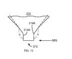
- FIGS. 12-13depict an exemplary embodiment of a PMR transducer formed using one or more of the optical masks 100 , 110 , 120 , 130 , and 140 , resist mask 160 , and the method 150 , particularly step 156 .
- FIG. 12depicts an ABS view of an exemplary embodiment of a PMR transducer 200 .
- FIG. 13depicts a top view of an exemplary embodiment of the PMR pole.
- the method 150 and optical masks 100 , 110 , 120 , 130 , and 140might be used for other electronic devices.
- the device features 101 , 111 , 121 , 131 , and 141may have different configurations.
- the PMR transducer 200 shown in FIGS. 12-13is typically used as a write head in a merged head including the PMR transducer 200 and a read head.
- the PMR transducer 200includes a first pole 202 , insulator 204 , insulator 206 , a PMR pole (main pole) 210 , write gap 208 , and a top shield 209 .
- the PMR pole 210has a negative angle, ⁇ . Thus, the top of the PMR pole 210 is wider than the bottom of the PMR pole 210 . Near the ABS, the PMR pole 210 terminates in a nose 212 .
- the PMR pole 210thus flares outward from the nose 212 at a flare angle, ⁇ , forming corners 214 A and 214 B.
- the flare anglemay be between approximately one hundred ten degrees and one hundred sixty degrees in one embodiment. In another embodiment, the flare angle may be approximately one hundred and fifty degrees.
- optical proximity effectsmay be reduced or eliminated for the mask 160 and thus the PMR pole 210 .
- the corners 214 A and 214 B of the PMR pole 210may have significantly less rounding. Consequently, the geometry of the nose 212 may be closer to what is desired.
- the control of the track width of the PMR transducer 200 and the geometry of the nose 212may be improved. Consequently, performance and/or reliability of the magnetic transducer formed.
- the method 150 , masks 100 / 110 / 120 / 130 / 140 , and resist mask 160may be extended to other structures in a magnetic recording transducer, or other electronic devices, which include corners. As a result, performance of the magnetic transducer, as well as other electronic devices, may be further enhanced.
- a method and system for providing a mask and, therefore, a portion of a magnetic recording transducerhas been disclosed. Using the method and system, a structure having sharper corners, improved geometry control and, therefore, a better defined track width has been described.
Landscapes
- Physics & Mathematics (AREA)
- General Physics & Mathematics (AREA)
- Preparing Plates And Mask In Photomechanical Process (AREA)
Abstract
Description
Claims (26)
Priority Applications (1)
| Application Number | Priority Date | Filing Date | Title |
|---|---|---|---|
| US12/333,699US7910267B1 (en) | 2008-12-12 | 2008-12-12 | Method and system for providing optical proximity correction for structures such as a PMR nose |
Applications Claiming Priority (1)
| Application Number | Priority Date | Filing Date | Title |
|---|---|---|---|
| US12/333,699US7910267B1 (en) | 2008-12-12 | 2008-12-12 | Method and system for providing optical proximity correction for structures such as a PMR nose |
Publications (1)
| Publication Number | Publication Date |
|---|---|
| US7910267B1true US7910267B1 (en) | 2011-03-22 |
Family
ID=43741734
Family Applications (1)
| Application Number | Title | Priority Date | Filing Date |
|---|---|---|---|
| US12/333,699Expired - Fee RelatedUS7910267B1 (en) | 2008-12-12 | 2008-12-12 | Method and system for providing optical proximity correction for structures such as a PMR nose |
Country Status (1)
| Country | Link |
|---|---|
| US (1) | US7910267B1 (en) |
Cited By (131)
| Publication number | Priority date | Publication date | Assignee | Title |
|---|---|---|---|---|
| US8830628B1 (en) | 2009-02-23 | 2014-09-09 | Western Digital (Fremont), Llc | Method and system for providing a perpendicular magnetic recording head |
| US8879207B1 (en) | 2011-12-20 | 2014-11-04 | Western Digital (Fremont), Llc | Method for providing a side shield for a magnetic recording transducer using an air bridge |
| US8883017B1 (en) | 2013-03-12 | 2014-11-11 | Western Digital (Fremont), Llc | Method and system for providing a read transducer having seamless interfaces |
| US8917581B1 (en) | 2013-12-18 | 2014-12-23 | Western Digital Technologies, Inc. | Self-anneal process for a near field transducer and chimney in a hard disk drive assembly |
| US8923102B1 (en) | 2013-07-16 | 2014-12-30 | Western Digital (Fremont), Llc | Optical grating coupling for interferometric waveguides in heat assisted magnetic recording heads |
| US8947985B1 (en) | 2013-07-16 | 2015-02-03 | Western Digital (Fremont), Llc | Heat assisted magnetic recording transducers having a recessed pole |
| US8953422B1 (en) | 2014-06-10 | 2015-02-10 | Western Digital (Fremont), Llc | Near field transducer using dielectric waveguide core with fine ridge feature |
| US8958272B1 (en) | 2014-06-10 | 2015-02-17 | Western Digital (Fremont), Llc | Interfering near field transducer for energy assisted magnetic recording |
| US8970988B1 (en) | 2013-12-31 | 2015-03-03 | Western Digital (Fremont), Llc | Electric gaps and method for making electric gaps for multiple sensor arrays |
| US8971160B1 (en) | 2013-12-19 | 2015-03-03 | Western Digital (Fremont), Llc | Near field transducer with high refractive index pin for heat assisted magnetic recording |
| US8976635B1 (en) | 2014-06-10 | 2015-03-10 | Western Digital (Fremont), Llc | Near field transducer driven by a transverse electric waveguide for energy assisted magnetic recording |
| US8980109B1 (en) | 2012-12-11 | 2015-03-17 | Western Digital (Fremont), Llc | Method for providing a magnetic recording transducer using a combined main pole and side shield CMP for a wraparound shield scheme |
| US8982508B1 (en) | 2011-10-31 | 2015-03-17 | Western Digital (Fremont), Llc | Method for providing a side shield for a magnetic recording transducer |
| US8988812B1 (en) | 2013-11-27 | 2015-03-24 | Western Digital (Fremont), Llc | Multi-sensor array configuration for a two-dimensional magnetic recording (TDMR) operation |
| US8984740B1 (en) | 2012-11-30 | 2015-03-24 | Western Digital (Fremont), Llc | Process for providing a magnetic recording transducer having a smooth magnetic seed layer |
| US8988825B1 (en) | 2014-02-28 | 2015-03-24 | Western Digital (Fremont, LLC | Method for fabricating a magnetic writer having half-side shields |
| US8995087B1 (en) | 2006-11-29 | 2015-03-31 | Western Digital (Fremont), Llc | Perpendicular magnetic recording write head having a wrap around shield |
| US8993217B1 (en) | 2013-04-04 | 2015-03-31 | Western Digital (Fremont), Llc | Double exposure technique for high resolution disk imaging |
| US9001467B1 (en) | 2014-03-05 | 2015-04-07 | Western Digital (Fremont), Llc | Method for fabricating side shields in a magnetic writer |
| US9001628B1 (en) | 2013-12-16 | 2015-04-07 | Western Digital (Fremont), Llc | Assistant waveguides for evaluating main waveguide coupling efficiency and diode laser alignment tolerances for hard disk |
| US8997832B1 (en) | 2010-11-23 | 2015-04-07 | Western Digital (Fremont), Llc | Method of fabricating micrometer scale components |
| US9007879B1 (en) | 2014-06-10 | 2015-04-14 | Western Digital (Fremont), Llc | Interfering near field transducer having a wide metal bar feature for energy assisted magnetic recording |
| US9007719B1 (en) | 2013-10-23 | 2015-04-14 | Western Digital (Fremont), Llc | Systems and methods for using double mask techniques to achieve very small features |
| US9007725B1 (en) | 2014-10-07 | 2015-04-14 | Western Digital (Fremont), Llc | Sensor with positive coupling between dual ferromagnetic free layer laminates |
| US9013836B1 (en) | 2013-04-02 | 2015-04-21 | Western Digital (Fremont), Llc | Method and system for providing an antiferromagnetically coupled return pole |
| US9042058B1 (en) | 2013-10-17 | 2015-05-26 | Western Digital Technologies, Inc. | Shield designed for middle shields in a multiple sensor array |
| US9042051B2 (en) | 2013-08-15 | 2015-05-26 | Western Digital (Fremont), Llc | Gradient write gap for perpendicular magnetic recording writer |
| US9042057B1 (en) | 2013-01-09 | 2015-05-26 | Western Digital (Fremont), Llc | Methods for providing magnetic storage elements with high magneto-resistance using Heusler alloys |
| US9042052B1 (en) | 2014-06-23 | 2015-05-26 | Western Digital (Fremont), Llc | Magnetic writer having a partially shunted coil |
| US9042208B1 (en) | 2013-03-11 | 2015-05-26 | Western Digital Technologies, Inc. | Disk drive measuring fly height by applying a bias voltage to an electrically insulated write component of a head |
| US9053735B1 (en) | 2014-06-20 | 2015-06-09 | Western Digital (Fremont), Llc | Method for fabricating a magnetic writer using a full-film metal planarization |
| US9064528B1 (en) | 2013-05-17 | 2015-06-23 | Western Digital Technologies, Inc. | Interferometric waveguide usable in shingled heat assisted magnetic recording in the absence of a near-field transducer |
| US9064527B1 (en) | 2013-04-12 | 2015-06-23 | Western Digital (Fremont), Llc | High order tapered waveguide for use in a heat assisted magnetic recording head |
| US9065043B1 (en) | 2012-06-29 | 2015-06-23 | Western Digital (Fremont), Llc | Tunnel magnetoresistance read head with narrow shield-to-shield spacing |
| US9064507B1 (en) | 2009-07-31 | 2015-06-23 | Western Digital (Fremont), Llc | Magnetic etch-stop layer for magnetoresistive read heads |
| US9070381B1 (en) | 2013-04-12 | 2015-06-30 | Western Digital (Fremont), Llc | Magnetic recording read transducer having a laminated free layer |
| US9082423B1 (en) | 2013-12-18 | 2015-07-14 | Western Digital (Fremont), Llc | Magnetic recording write transducer having an improved trailing surface profile |
| US9087527B1 (en) | 2014-10-28 | 2015-07-21 | Western Digital (Fremont), Llc | Apparatus and method for middle shield connection in magnetic recording transducers |
| US9087534B1 (en) | 2011-12-20 | 2015-07-21 | Western Digital (Fremont), Llc | Method and system for providing a read transducer having soft and hard magnetic bias structures |
| US9093639B2 (en) | 2012-02-21 | 2015-07-28 | Western Digital (Fremont), Llc | Methods for manufacturing a magnetoresistive structure utilizing heating and cooling |
| US9104107B1 (en) | 2013-04-03 | 2015-08-11 | Western Digital (Fremont), Llc | DUV photoresist process |
| US9111558B1 (en) | 2014-03-14 | 2015-08-18 | Western Digital (Fremont), Llc | System and method of diffractive focusing of light in a waveguide |
| US9111564B1 (en) | 2013-04-02 | 2015-08-18 | Western Digital (Fremont), Llc | Magnetic recording writer having a main pole with multiple flare angles |
| US9111550B1 (en) | 2014-12-04 | 2015-08-18 | Western Digital (Fremont), Llc | Write transducer having a magnetic buffer layer spaced between a side shield and a write pole by non-magnetic layers |
| US9123362B1 (en) | 2011-03-22 | 2015-09-01 | Western Digital (Fremont), Llc | Methods for assembling an electrically assisted magnetic recording (EAMR) head |
| US9123374B1 (en) | 2015-02-12 | 2015-09-01 | Western Digital (Fremont), Llc | Heat assisted magnetic recording writer having an integrated polarization rotation plate |
| US9123359B1 (en) | 2010-12-22 | 2015-09-01 | Western Digital (Fremont), Llc | Magnetic recording transducer with sputtered antiferromagnetic coupling trilayer between plated ferromagnetic shields and method of fabrication |
| US9123358B1 (en) | 2012-06-11 | 2015-09-01 | Western Digital (Fremont), Llc | Conformal high moment side shield seed layer for perpendicular magnetic recording writer |
| US9135937B1 (en) | 2014-05-09 | 2015-09-15 | Western Digital (Fremont), Llc | Current modulation on laser diode for energy assisted magnetic recording transducer |
| US9135930B1 (en) | 2014-03-06 | 2015-09-15 | Western Digital (Fremont), Llc | Method for fabricating a magnetic write pole using vacuum deposition |
| US9142233B1 (en) | 2014-02-28 | 2015-09-22 | Western Digital (Fremont), Llc | Heat assisted magnetic recording writer having a recessed pole |
| US9147408B1 (en) | 2013-12-19 | 2015-09-29 | Western Digital (Fremont), Llc | Heated AFM layer deposition and cooling process for TMR magnetic recording sensor with high pinning field |
| US9147404B1 (en) | 2015-03-31 | 2015-09-29 | Western Digital (Fremont), Llc | Method and system for providing a read transducer having a dual free layer |
| US9153255B1 (en) | 2014-03-05 | 2015-10-06 | Western Digital (Fremont), Llc | Method for fabricating a magnetic writer having an asymmetric gap and shields |
| US9183854B2 (en) | 2014-02-24 | 2015-11-10 | Western Digital (Fremont), Llc | Method to make interferometric taper waveguide for HAMR light delivery |
| US9190085B1 (en) | 2014-03-12 | 2015-11-17 | Western Digital (Fremont), Llc | Waveguide with reflective grating for localized energy intensity |
| US9190079B1 (en) | 2014-09-22 | 2015-11-17 | Western Digital (Fremont), Llc | Magnetic write pole having engineered radius of curvature and chisel angle profiles |
| US9194692B1 (en) | 2013-12-06 | 2015-11-24 | Western Digital (Fremont), Llc | Systems and methods for using white light interferometry to measure undercut of a bi-layer structure |
| US9202480B2 (en) | 2009-10-14 | 2015-12-01 | Western Digital (Fremont), LLC. | Double patterning hard mask for damascene perpendicular magnetic recording (PMR) writer |
| US9202493B1 (en) | 2014-02-28 | 2015-12-01 | Western Digital (Fremont), Llc | Method of making an ultra-sharp tip mode converter for a HAMR head |
| US9213322B1 (en) | 2012-08-16 | 2015-12-15 | Western Digital (Fremont), Llc | Methods for providing run to run process control using a dynamic tuner |
| US9214172B2 (en) | 2013-10-23 | 2015-12-15 | Western Digital (Fremont), Llc | Method of manufacturing a magnetic read head |
| US9214169B1 (en) | 2014-06-20 | 2015-12-15 | Western Digital (Fremont), Llc | Magnetic recording read transducer having a laminated free layer |
| US9214165B1 (en) | 2014-12-18 | 2015-12-15 | Western Digital (Fremont), Llc | Magnetic writer having a gradient in saturation magnetization of the shields |
| US9230565B1 (en) | 2014-06-24 | 2016-01-05 | Western Digital (Fremont), Llc | Magnetic shield for magnetic recording head |
| US9236560B1 (en) | 2014-12-08 | 2016-01-12 | Western Digital (Fremont), Llc | Spin transfer torque tunneling magnetoresistive device having a laminated free layer with perpendicular magnetic anisotropy |
| US9245543B1 (en) | 2010-06-25 | 2016-01-26 | Western Digital (Fremont), Llc | Method for providing an energy assisted magnetic recording head having a laser integrally mounted to the slider |
| US9245562B1 (en) | 2015-03-30 | 2016-01-26 | Western Digital (Fremont), Llc | Magnetic recording writer with a composite main pole |
| US9245545B1 (en) | 2013-04-12 | 2016-01-26 | Wester Digital (Fremont), Llc | Short yoke length coils for magnetic heads in disk drives |
| US9251813B1 (en) | 2009-04-19 | 2016-02-02 | Western Digital (Fremont), Llc | Method of making a magnetic recording head |
| US9263071B1 (en) | 2015-03-31 | 2016-02-16 | Western Digital (Fremont), Llc | Flat NFT for heat assisted magnetic recording |
| US9263067B1 (en) | 2013-05-29 | 2016-02-16 | Western Digital (Fremont), Llc | Process for making PMR writer with constant side wall angle |
| US9269382B1 (en) | 2012-06-29 | 2016-02-23 | Western Digital (Fremont), Llc | Method and system for providing a read transducer having improved pinning of the pinned layer at higher recording densities |
| US9275657B1 (en) | 2013-08-14 | 2016-03-01 | Western Digital (Fremont), Llc | Process for making PMR writer with non-conformal side gaps |
| US9280990B1 (en) | 2013-12-11 | 2016-03-08 | Western Digital (Fremont), Llc | Method for fabricating a magnetic writer using multiple etches |
| US9286919B1 (en) | 2014-12-17 | 2016-03-15 | Western Digital (Fremont), Llc | Magnetic writer having a dual side gap |
| US9287494B1 (en) | 2013-06-28 | 2016-03-15 | Western Digital (Fremont), Llc | Magnetic tunnel junction (MTJ) with a magnesium oxide tunnel barrier |
| US9305583B1 (en) | 2014-02-18 | 2016-04-05 | Western Digital (Fremont), Llc | Method for fabricating a magnetic writer using multiple etches of damascene materials |
| US9312064B1 (en) | 2015-03-02 | 2016-04-12 | Western Digital (Fremont), Llc | Method to fabricate a magnetic head including ion milling of read gap using dual layer hard mask |
| US9318130B1 (en) | 2013-07-02 | 2016-04-19 | Western Digital (Fremont), Llc | Method to fabricate tunneling magnetic recording heads with extended pinned layer |
| US9336814B1 (en) | 2013-03-12 | 2016-05-10 | Western Digital (Fremont), Llc | Inverse tapered waveguide for use in a heat assisted magnetic recording head |
| US9343086B1 (en) | 2013-09-11 | 2016-05-17 | Western Digital (Fremont), Llc | Magnetic recording write transducer having an improved sidewall angle profile |
| US9343098B1 (en) | 2013-08-23 | 2016-05-17 | Western Digital (Fremont), Llc | Method for providing a heat assisted magnetic recording transducer having protective pads |
| US9343087B1 (en) | 2014-12-21 | 2016-05-17 | Western Digital (Fremont), Llc | Method for fabricating a magnetic writer having half shields |
| US9349392B1 (en) | 2012-05-24 | 2016-05-24 | Western Digital (Fremont), Llc | Methods for improving adhesion on dielectric substrates |
| US9349394B1 (en) | 2013-10-18 | 2016-05-24 | Western Digital (Fremont), Llc | Method for fabricating a magnetic writer having a gradient side gap |
| US9361913B1 (en) | 2013-06-03 | 2016-06-07 | Western Digital (Fremont), Llc | Recording read heads with a multi-layer AFM layer methods and apparatuses |
| US9361914B1 (en) | 2014-06-18 | 2016-06-07 | Western Digital (Fremont), Llc | Magnetic sensor with thin capping layer |
| US9368134B1 (en) | 2010-12-16 | 2016-06-14 | Western Digital (Fremont), Llc | Method and system for providing an antiferromagnetically coupled writer |
| US9384765B1 (en) | 2015-09-24 | 2016-07-05 | Western Digital (Fremont), Llc | Method and system for providing a HAMR writer having improved optical efficiency |
| US9384763B1 (en) | 2015-03-26 | 2016-07-05 | Western Digital (Fremont), Llc | Dual free layer magnetic reader having a rear bias structure including a soft bias layer |
| US9396743B1 (en) | 2014-02-28 | 2016-07-19 | Western Digital (Fremont), Llc | Systems and methods for controlling soft bias thickness for tunnel magnetoresistance readers |
| US9396742B1 (en) | 2012-11-30 | 2016-07-19 | Western Digital (Fremont), Llc | Magnetoresistive sensor for a magnetic storage system read head, and fabrication method thereof |
| US9406331B1 (en) | 2013-06-17 | 2016-08-02 | Western Digital (Fremont), Llc | Method for making ultra-narrow read sensor and read transducer device resulting therefrom |
| US9424866B1 (en) | 2015-09-24 | 2016-08-23 | Western Digital (Fremont), Llc | Heat assisted magnetic recording write apparatus having a dielectric gap |
| US9431039B1 (en) | 2013-05-21 | 2016-08-30 | Western Digital (Fremont), Llc | Multiple sensor array usable in two-dimensional magnetic recording |
| US9431032B1 (en) | 2013-08-14 | 2016-08-30 | Western Digital (Fremont), Llc | Electrical connection arrangement for a multiple sensor array usable in two-dimensional magnetic recording |
| US9431038B1 (en) | 2015-06-29 | 2016-08-30 | Western Digital (Fremont), Llc | Method for fabricating a magnetic write pole having an improved sidewall angle profile |
| US9431031B1 (en) | 2015-03-24 | 2016-08-30 | Western Digital (Fremont), Llc | System and method for magnetic transducers having multiple sensors and AFC shields |
| US9431047B1 (en) | 2013-05-01 | 2016-08-30 | Western Digital (Fremont), Llc | Method for providing an improved AFM reader shield |
| US9437251B1 (en) | 2014-12-22 | 2016-09-06 | Western Digital (Fremont), Llc | Apparatus and method having TDMR reader to reader shunts |
| US9443541B1 (en) | 2015-03-24 | 2016-09-13 | Western Digital (Fremont), Llc | Magnetic writer having a gradient in saturation magnetization of the shields and return pole |
| US9441938B1 (en) | 2013-10-08 | 2016-09-13 | Western Digital (Fremont), Llc | Test structures for measuring near field transducer disc length |
| US9449625B1 (en) | 2014-12-24 | 2016-09-20 | Western Digital (Fremont), Llc | Heat assisted magnetic recording head having a plurality of diffusion barrier layers |
| US9449621B1 (en) | 2015-03-26 | 2016-09-20 | Western Digital (Fremont), Llc | Dual free layer magnetic reader having a rear bias structure having a high aspect ratio |
| US9472216B1 (en) | 2015-09-23 | 2016-10-18 | Western Digital (Fremont), Llc | Differential dual free layer magnetic reader |
| US9484051B1 (en) | 2015-11-09 | 2016-11-01 | The Provost, Fellows, Foundation Scholars and the other members of Board, of the College of the Holy and Undivided Trinity of Queen Elizabeth near Dublin | Method and system for reducing undesirable reflections in a HAMR write apparatus |
| US9508372B1 (en) | 2015-06-03 | 2016-11-29 | Western Digital (Fremont), Llc | Shingle magnetic writer having a low sidewall angle pole |
| US9508363B1 (en) | 2014-06-17 | 2016-11-29 | Western Digital (Fremont), Llc | Method for fabricating a magnetic write pole having a leading edge bevel |
| US9508365B1 (en) | 2015-06-24 | 2016-11-29 | Western Digital (Fremont), LLC. | Magnetic reader having a crystal decoupling structure |
| US9530443B1 (en) | 2015-06-25 | 2016-12-27 | Western Digital (Fremont), Llc | Method for fabricating a magnetic recording device having a high aspect ratio structure |
| US9564150B1 (en) | 2015-11-24 | 2017-02-07 | Western Digital (Fremont), Llc | Magnetic read apparatus having an improved read sensor isolation circuit |
| US9595273B1 (en) | 2015-09-30 | 2017-03-14 | Western Digital (Fremont), Llc | Shingle magnetic writer having nonconformal shields |
| US9646639B2 (en) | 2015-06-26 | 2017-05-09 | Western Digital (Fremont), Llc | Heat assisted magnetic recording writer having integrated polarization rotation waveguides |
| US9666214B1 (en) | 2015-09-23 | 2017-05-30 | Western Digital (Fremont), Llc | Free layer magnetic reader that may have a reduced shield-to-shield spacing |
| US9721595B1 (en) | 2014-12-04 | 2017-08-01 | Western Digital (Fremont), Llc | Method for providing a storage device |
| US9740805B1 (en) | 2015-12-01 | 2017-08-22 | Western Digital (Fremont), Llc | Method and system for detecting hotspots for photolithographically-defined devices |
| US9741366B1 (en) | 2014-12-18 | 2017-08-22 | Western Digital (Fremont), Llc | Method for fabricating a magnetic writer having a gradient in saturation magnetization of the shields |
| US9754611B1 (en) | 2015-11-30 | 2017-09-05 | Western Digital (Fremont), Llc | Magnetic recording write apparatus having a stepped conformal trailing shield |
| US9767831B1 (en) | 2015-12-01 | 2017-09-19 | Western Digital (Fremont), Llc | Magnetic writer having convex trailing surface pole and conformal write gap |
| US9786301B1 (en) | 2014-12-02 | 2017-10-10 | Western Digital (Fremont), Llc | Apparatuses and methods for providing thin shields in a multiple sensor array |
| US9799351B1 (en) | 2015-11-30 | 2017-10-24 | Western Digital (Fremont), Llc | Short yoke length writer having assist coils |
| US9812155B1 (en) | 2015-11-23 | 2017-11-07 | Western Digital (Fremont), Llc | Method and system for fabricating high junction angle read sensors |
| US9842615B1 (en) | 2015-06-26 | 2017-12-12 | Western Digital (Fremont), Llc | Magnetic reader having a nonmagnetic insertion layer for the pinning layer |
| US9858951B1 (en) | 2015-12-01 | 2018-01-02 | Western Digital (Fremont), Llc | Method for providing a multilayer AFM layer in a read sensor |
| US9881638B1 (en) | 2014-12-17 | 2018-01-30 | Western Digital (Fremont), Llc | Method for providing a near-field transducer (NFT) for a heat assisted magnetic recording (HAMR) device |
| US9934811B1 (en) | 2014-03-07 | 2018-04-03 | Western Digital (Fremont), Llc | Methods for controlling stray fields of magnetic features using magneto-elastic anisotropy |
| US9953670B1 (en) | 2015-11-10 | 2018-04-24 | Western Digital (Fremont), Llc | Method and system for providing a HAMR writer including a multi-mode interference device |
| US10037770B1 (en) | 2015-11-12 | 2018-07-31 | Western Digital (Fremont), Llc | Method for providing a magnetic recording write apparatus having a seamless pole |
| US10074387B1 (en) | 2014-12-21 | 2018-09-11 | Western Digital (Fremont), Llc | Method and system for providing a read transducer having symmetric antiferromagnetically coupled shields |
| US20240027892A1 (en)* | 2022-07-22 | 2024-01-25 | Western Digital Technologies, Inc. | Method of making a hard disk drive write pole using a tri-tone attenuated phase shift mask |
Citations (19)
| Publication number | Priority date | Publication date | Assignee | Title |
|---|---|---|---|---|
| US5242770A (en) | 1992-01-16 | 1993-09-07 | Microunity Systems Engineering, Inc. | Mask for photolithography |
| US5849440A (en)* | 1996-07-02 | 1998-12-15 | Motorola, Inc. | Process for producing and inspecting a lithographic reticle and fabricating semiconductor devices using same |
| US6127071A (en) | 1999-06-22 | 2000-10-03 | International Business Machines Corporation | Serif mask design for correcting severe corner rounding and line end shortening in lithography |
| US6178066B1 (en) | 1998-05-27 | 2001-01-23 | Read-Rite Corporation | Method of fabricating an improved thin film device having a small element with well defined corners |
| US6255130B1 (en)* | 1998-11-19 | 2001-07-03 | Samsung Electronics Co., Ltd. | Thin film transistor array panel and a method for manufacturing the same |
| US6255040B1 (en)* | 1999-03-24 | 2001-07-03 | Tdk Corporation | Method of manufacturing thin film magnetic head |
| US6280887B1 (en) | 2000-03-02 | 2001-08-28 | International Business Machines Corporation | Complementary and exchange mask design methodology for optical proximity correction in microlithography |
| US20020157081A1 (en) | 2001-02-28 | 2002-10-24 | Xuelong Shi | Method of identifying an extreme interaction pitch region, methods of designing mask patterns and manufacturing masks, device manufacturing methods and computer programs |
| US6492078B1 (en) | 1999-02-16 | 2002-12-10 | Sony Corporation | Correcting method of exposure pattern, exposure method, exposure system, photomask and semiconductor device |
| US6497825B1 (en) | 1999-09-08 | 2002-12-24 | Tdk Corporation | Manufacturing method of thin-film magnetic head |
| US7141338B2 (en) | 2002-11-12 | 2006-11-28 | Infineon Technologies Ag | Sub-resolution sized assist features |
| US20060269848A1 (en)* | 2005-05-31 | 2006-11-30 | Fujitsu Limited | Exposure mask and method of manufacturing the same, and semiconductor device manufacturing method |
| US20070134597A1 (en) | 2005-12-08 | 2007-06-14 | Headway Technologies, Inc. | Process to form an isolated trench image in photoresist |
| US7252909B2 (en) | 2002-04-18 | 2007-08-07 | Taiwan Semiconductor Manufacturing Co., Ltd. | Method to reduce CD non-uniformity in IC manufacturing |
| US20070279802A1 (en) | 2006-05-31 | 2007-12-06 | Headway Technologies, Inc. | Magnetic head and method of manufacturing same, and method of forming patterned layer |
| US20080073718A1 (en)* | 2006-09-27 | 2008-03-27 | Young-Wook Lee | Mask for forming a thin-film transistor, thin-film transistor substrate manufactured using the same and method of manufacturing a thin-film transistor substrate using the same |
| US20080206656A1 (en)* | 2003-06-30 | 2008-08-28 | Asml Masktools B.V. | Scattering bar OPC application method for sub-half wavelength lithography patterning |
| US20090068572A1 (en)* | 2007-09-10 | 2009-03-12 | Beijing Boe Optoelectronics Technology Co., Ltd.. | Gray scale mask |
| US7736823B1 (en)* | 2007-05-11 | 2010-06-15 | Western Digital (Fremont), Llc | Method and system for providing optical proximity correction for structures such as a PMR nose |
- 2008
- 2008-12-12USUS12/333,699patent/US7910267B1/ennot_activeExpired - Fee Related
Patent Citations (20)
| Publication number | Priority date | Publication date | Assignee | Title |
|---|---|---|---|---|
| US5242770A (en) | 1992-01-16 | 1993-09-07 | Microunity Systems Engineering, Inc. | Mask for photolithography |
| US5849440A (en)* | 1996-07-02 | 1998-12-15 | Motorola, Inc. | Process for producing and inspecting a lithographic reticle and fabricating semiconductor devices using same |
| US6178066B1 (en) | 1998-05-27 | 2001-01-23 | Read-Rite Corporation | Method of fabricating an improved thin film device having a small element with well defined corners |
| US6255130B1 (en)* | 1998-11-19 | 2001-07-03 | Samsung Electronics Co., Ltd. | Thin film transistor array panel and a method for manufacturing the same |
| US6492078B1 (en) | 1999-02-16 | 2002-12-10 | Sony Corporation | Correcting method of exposure pattern, exposure method, exposure system, photomask and semiconductor device |
| US6255040B1 (en)* | 1999-03-24 | 2001-07-03 | Tdk Corporation | Method of manufacturing thin film magnetic head |
| US6127071A (en) | 1999-06-22 | 2000-10-03 | International Business Machines Corporation | Serif mask design for correcting severe corner rounding and line end shortening in lithography |
| US6497825B1 (en) | 1999-09-08 | 2002-12-24 | Tdk Corporation | Manufacturing method of thin-film magnetic head |
| US6280887B1 (en) | 2000-03-02 | 2001-08-28 | International Business Machines Corporation | Complementary and exchange mask design methodology for optical proximity correction in microlithography |
| US7100145B2 (en) | 2001-02-28 | 2006-08-29 | Asml Masktools B.V. | Method of identifying an extreme interaction pitch region, methods of designing mask patterns and manufacturing masks, device manufacturing methods and computer programs |
| US20020157081A1 (en) | 2001-02-28 | 2002-10-24 | Xuelong Shi | Method of identifying an extreme interaction pitch region, methods of designing mask patterns and manufacturing masks, device manufacturing methods and computer programs |
| US7252909B2 (en) | 2002-04-18 | 2007-08-07 | Taiwan Semiconductor Manufacturing Co., Ltd. | Method to reduce CD non-uniformity in IC manufacturing |
| US7141338B2 (en) | 2002-11-12 | 2006-11-28 | Infineon Technologies Ag | Sub-resolution sized assist features |
| US20080206656A1 (en)* | 2003-06-30 | 2008-08-28 | Asml Masktools B.V. | Scattering bar OPC application method for sub-half wavelength lithography patterning |
| US20060269848A1 (en)* | 2005-05-31 | 2006-11-30 | Fujitsu Limited | Exposure mask and method of manufacturing the same, and semiconductor device manufacturing method |
| US20070134597A1 (en) | 2005-12-08 | 2007-06-14 | Headway Technologies, Inc. | Process to form an isolated trench image in photoresist |
| US20070279802A1 (en) | 2006-05-31 | 2007-12-06 | Headway Technologies, Inc. | Magnetic head and method of manufacturing same, and method of forming patterned layer |
| US20080073718A1 (en)* | 2006-09-27 | 2008-03-27 | Young-Wook Lee | Mask for forming a thin-film transistor, thin-film transistor substrate manufactured using the same and method of manufacturing a thin-film transistor substrate using the same |
| US7736823B1 (en)* | 2007-05-11 | 2010-06-15 | Western Digital (Fremont), Llc | Method and system for providing optical proximity correction for structures such as a PMR nose |
| US20090068572A1 (en)* | 2007-09-10 | 2009-03-12 | Beijing Boe Optoelectronics Technology Co., Ltd.. | Gray scale mask |
Cited By (154)
| Publication number | Priority date | Publication date | Assignee | Title |
|---|---|---|---|---|
| US8995087B1 (en) | 2006-11-29 | 2015-03-31 | Western Digital (Fremont), Llc | Perpendicular magnetic recording write head having a wrap around shield |
| US8830628B1 (en) | 2009-02-23 | 2014-09-09 | Western Digital (Fremont), Llc | Method and system for providing a perpendicular magnetic recording head |
| US9251813B1 (en) | 2009-04-19 | 2016-02-02 | Western Digital (Fremont), Llc | Method of making a magnetic recording head |
| US9064507B1 (en) | 2009-07-31 | 2015-06-23 | Western Digital (Fremont), Llc | Magnetic etch-stop layer for magnetoresistive read heads |
| US9202480B2 (en) | 2009-10-14 | 2015-12-01 | Western Digital (Fremont), LLC. | Double patterning hard mask for damascene perpendicular magnetic recording (PMR) writer |
| US9245543B1 (en) | 2010-06-25 | 2016-01-26 | Western Digital (Fremont), Llc | Method for providing an energy assisted magnetic recording head having a laser integrally mounted to the slider |
| US8997832B1 (en) | 2010-11-23 | 2015-04-07 | Western Digital (Fremont), Llc | Method of fabricating micrometer scale components |
| US9159345B1 (en) | 2010-11-23 | 2015-10-13 | Western Digital (Fremont), Llc | Micrometer scale components |
| US9672847B2 (en) | 2010-11-23 | 2017-06-06 | Western Digital (Fremont), Llc | Micrometer scale components |
| US9368134B1 (en) | 2010-12-16 | 2016-06-14 | Western Digital (Fremont), Llc | Method and system for providing an antiferromagnetically coupled writer |
| US9123359B1 (en) | 2010-12-22 | 2015-09-01 | Western Digital (Fremont), Llc | Magnetic recording transducer with sputtered antiferromagnetic coupling trilayer between plated ferromagnetic shields and method of fabrication |
| US9123362B1 (en) | 2011-03-22 | 2015-09-01 | Western Digital (Fremont), Llc | Methods for assembling an electrically assisted magnetic recording (EAMR) head |
| US8982508B1 (en) | 2011-10-31 | 2015-03-17 | Western Digital (Fremont), Llc | Method for providing a side shield for a magnetic recording transducer |
| US9087534B1 (en) | 2011-12-20 | 2015-07-21 | Western Digital (Fremont), Llc | Method and system for providing a read transducer having soft and hard magnetic bias structures |
| US8879207B1 (en) | 2011-12-20 | 2014-11-04 | Western Digital (Fremont), Llc | Method for providing a side shield for a magnetic recording transducer using an air bridge |
| US9093639B2 (en) | 2012-02-21 | 2015-07-28 | Western Digital (Fremont), Llc | Methods for manufacturing a magnetoresistive structure utilizing heating and cooling |
| US9349392B1 (en) | 2012-05-24 | 2016-05-24 | Western Digital (Fremont), Llc | Methods for improving adhesion on dielectric substrates |
| US9940950B2 (en) | 2012-05-24 | 2018-04-10 | Western Digital (Fremont), Llc | Methods for improving adhesion on dielectric substrates |
| US9123358B1 (en) | 2012-06-11 | 2015-09-01 | Western Digital (Fremont), Llc | Conformal high moment side shield seed layer for perpendicular magnetic recording writer |
| US9269382B1 (en) | 2012-06-29 | 2016-02-23 | Western Digital (Fremont), Llc | Method and system for providing a read transducer having improved pinning of the pinned layer at higher recording densities |
| US9412400B2 (en) | 2012-06-29 | 2016-08-09 | Western Digital (Fremont), Llc | Tunnel magnetoresistance read head with narrow shield-to-shield spacing |
| US9065043B1 (en) | 2012-06-29 | 2015-06-23 | Western Digital (Fremont), Llc | Tunnel magnetoresistance read head with narrow shield-to-shield spacing |
| US9213322B1 (en) | 2012-08-16 | 2015-12-15 | Western Digital (Fremont), Llc | Methods for providing run to run process control using a dynamic tuner |
| US8984740B1 (en) | 2012-11-30 | 2015-03-24 | Western Digital (Fremont), Llc | Process for providing a magnetic recording transducer having a smooth magnetic seed layer |
| US9396742B1 (en) | 2012-11-30 | 2016-07-19 | Western Digital (Fremont), Llc | Magnetoresistive sensor for a magnetic storage system read head, and fabrication method thereof |
| US8980109B1 (en) | 2012-12-11 | 2015-03-17 | Western Digital (Fremont), Llc | Method for providing a magnetic recording transducer using a combined main pole and side shield CMP for a wraparound shield scheme |
| US9042057B1 (en) | 2013-01-09 | 2015-05-26 | Western Digital (Fremont), Llc | Methods for providing magnetic storage elements with high magneto-resistance using Heusler alloys |
| US9042208B1 (en) | 2013-03-11 | 2015-05-26 | Western Digital Technologies, Inc. | Disk drive measuring fly height by applying a bias voltage to an electrically insulated write component of a head |
| US9336814B1 (en) | 2013-03-12 | 2016-05-10 | Western Digital (Fremont), Llc | Inverse tapered waveguide for use in a heat assisted magnetic recording head |
| US8883017B1 (en) | 2013-03-12 | 2014-11-11 | Western Digital (Fremont), Llc | Method and system for providing a read transducer having seamless interfaces |
| US9013836B1 (en) | 2013-04-02 | 2015-04-21 | Western Digital (Fremont), Llc | Method and system for providing an antiferromagnetically coupled return pole |
| US9111564B1 (en) | 2013-04-02 | 2015-08-18 | Western Digital (Fremont), Llc | Magnetic recording writer having a main pole with multiple flare angles |
| US9104107B1 (en) | 2013-04-03 | 2015-08-11 | Western Digital (Fremont), Llc | DUV photoresist process |
| US8993217B1 (en) | 2013-04-04 | 2015-03-31 | Western Digital (Fremont), Llc | Double exposure technique for high resolution disk imaging |
| US9064527B1 (en) | 2013-04-12 | 2015-06-23 | Western Digital (Fremont), Llc | High order tapered waveguide for use in a heat assisted magnetic recording head |
| US9245545B1 (en) | 2013-04-12 | 2016-01-26 | Wester Digital (Fremont), Llc | Short yoke length coils for magnetic heads in disk drives |
| US9070381B1 (en) | 2013-04-12 | 2015-06-30 | Western Digital (Fremont), Llc | Magnetic recording read transducer having a laminated free layer |
| US9431047B1 (en) | 2013-05-01 | 2016-08-30 | Western Digital (Fremont), Llc | Method for providing an improved AFM reader shield |
| US9064528B1 (en) | 2013-05-17 | 2015-06-23 | Western Digital Technologies, Inc. | Interferometric waveguide usable in shingled heat assisted magnetic recording in the absence of a near-field transducer |
| US9431039B1 (en) | 2013-05-21 | 2016-08-30 | Western Digital (Fremont), Llc | Multiple sensor array usable in two-dimensional magnetic recording |
| US9263067B1 (en) | 2013-05-29 | 2016-02-16 | Western Digital (Fremont), Llc | Process for making PMR writer with constant side wall angle |
| US9361913B1 (en) | 2013-06-03 | 2016-06-07 | Western Digital (Fremont), Llc | Recording read heads with a multi-layer AFM layer methods and apparatuses |
| US9406331B1 (en) | 2013-06-17 | 2016-08-02 | Western Digital (Fremont), Llc | Method for making ultra-narrow read sensor and read transducer device resulting therefrom |
| US9287494B1 (en) | 2013-06-28 | 2016-03-15 | Western Digital (Fremont), Llc | Magnetic tunnel junction (MTJ) with a magnesium oxide tunnel barrier |
| US9318130B1 (en) | 2013-07-02 | 2016-04-19 | Western Digital (Fremont), Llc | Method to fabricate tunneling magnetic recording heads with extended pinned layer |
| US8947985B1 (en) | 2013-07-16 | 2015-02-03 | Western Digital (Fremont), Llc | Heat assisted magnetic recording transducers having a recessed pole |
| US8923102B1 (en) | 2013-07-16 | 2014-12-30 | Western Digital (Fremont), Llc | Optical grating coupling for interferometric waveguides in heat assisted magnetic recording heads |
| US9431032B1 (en) | 2013-08-14 | 2016-08-30 | Western Digital (Fremont), Llc | Electrical connection arrangement for a multiple sensor array usable in two-dimensional magnetic recording |
| US9275657B1 (en) | 2013-08-14 | 2016-03-01 | Western Digital (Fremont), Llc | Process for making PMR writer with non-conformal side gaps |
| US9042051B2 (en) | 2013-08-15 | 2015-05-26 | Western Digital (Fremont), Llc | Gradient write gap for perpendicular magnetic recording writer |
| US9343098B1 (en) | 2013-08-23 | 2016-05-17 | Western Digital (Fremont), Llc | Method for providing a heat assisted magnetic recording transducer having protective pads |
| US9343086B1 (en) | 2013-09-11 | 2016-05-17 | Western Digital (Fremont), Llc | Magnetic recording write transducer having an improved sidewall angle profile |
| US9441938B1 (en) | 2013-10-08 | 2016-09-13 | Western Digital (Fremont), Llc | Test structures for measuring near field transducer disc length |
| US9042058B1 (en) | 2013-10-17 | 2015-05-26 | Western Digital Technologies, Inc. | Shield designed for middle shields in a multiple sensor array |
| US9349394B1 (en) | 2013-10-18 | 2016-05-24 | Western Digital (Fremont), Llc | Method for fabricating a magnetic writer having a gradient side gap |
| US9830936B2 (en) | 2013-10-23 | 2017-11-28 | Western Digital (Fremont), Llc | Magnetic read head with antiferromagentic layer |
| US9007719B1 (en) | 2013-10-23 | 2015-04-14 | Western Digital (Fremont), Llc | Systems and methods for using double mask techniques to achieve very small features |
| US9214172B2 (en) | 2013-10-23 | 2015-12-15 | Western Digital (Fremont), Llc | Method of manufacturing a magnetic read head |
| US8988812B1 (en) | 2013-11-27 | 2015-03-24 | Western Digital (Fremont), Llc | Multi-sensor array configuration for a two-dimensional magnetic recording (TDMR) operation |
| US9194692B1 (en) | 2013-12-06 | 2015-11-24 | Western Digital (Fremont), Llc | Systems and methods for using white light interferometry to measure undercut of a bi-layer structure |
| US9280990B1 (en) | 2013-12-11 | 2016-03-08 | Western Digital (Fremont), Llc | Method for fabricating a magnetic writer using multiple etches |
| US9001628B1 (en) | 2013-12-16 | 2015-04-07 | Western Digital (Fremont), Llc | Assistant waveguides for evaluating main waveguide coupling efficiency and diode laser alignment tolerances for hard disk |
| US9082423B1 (en) | 2013-12-18 | 2015-07-14 | Western Digital (Fremont), Llc | Magnetic recording write transducer having an improved trailing surface profile |
| US8917581B1 (en) | 2013-12-18 | 2014-12-23 | Western Digital Technologies, Inc. | Self-anneal process for a near field transducer and chimney in a hard disk drive assembly |
| US8971160B1 (en) | 2013-12-19 | 2015-03-03 | Western Digital (Fremont), Llc | Near field transducer with high refractive index pin for heat assisted magnetic recording |
| US9147408B1 (en) | 2013-12-19 | 2015-09-29 | Western Digital (Fremont), Llc | Heated AFM layer deposition and cooling process for TMR magnetic recording sensor with high pinning field |
| US8970988B1 (en) | 2013-12-31 | 2015-03-03 | Western Digital (Fremont), Llc | Electric gaps and method for making electric gaps for multiple sensor arrays |
| US9305583B1 (en) | 2014-02-18 | 2016-04-05 | Western Digital (Fremont), Llc | Method for fabricating a magnetic writer using multiple etches of damascene materials |
| US9183854B2 (en) | 2014-02-24 | 2015-11-10 | Western Digital (Fremont), Llc | Method to make interferometric taper waveguide for HAMR light delivery |
| US9202493B1 (en) | 2014-02-28 | 2015-12-01 | Western Digital (Fremont), Llc | Method of making an ultra-sharp tip mode converter for a HAMR head |
| US9396743B1 (en) | 2014-02-28 | 2016-07-19 | Western Digital (Fremont), Llc | Systems and methods for controlling soft bias thickness for tunnel magnetoresistance readers |
| US9142233B1 (en) | 2014-02-28 | 2015-09-22 | Western Digital (Fremont), Llc | Heat assisted magnetic recording writer having a recessed pole |
| US8988825B1 (en) | 2014-02-28 | 2015-03-24 | Western Digital (Fremont, LLC | Method for fabricating a magnetic writer having half-side shields |
| US9153255B1 (en) | 2014-03-05 | 2015-10-06 | Western Digital (Fremont), Llc | Method for fabricating a magnetic writer having an asymmetric gap and shields |
| US9001467B1 (en) | 2014-03-05 | 2015-04-07 | Western Digital (Fremont), Llc | Method for fabricating side shields in a magnetic writer |
| US9349393B2 (en) | 2014-03-05 | 2016-05-24 | Western Digital (Fremont), Llc | Magnetic writer having an asymmetric gap and shields |
| US9135930B1 (en) | 2014-03-06 | 2015-09-15 | Western Digital (Fremont), Llc | Method for fabricating a magnetic write pole using vacuum deposition |
| US9934811B1 (en) | 2014-03-07 | 2018-04-03 | Western Digital (Fremont), Llc | Methods for controlling stray fields of magnetic features using magneto-elastic anisotropy |
| US9495984B2 (en) | 2014-03-12 | 2016-11-15 | Western Digital (Fremont), Llc | Waveguide with reflective grating for localized energy intensity |
| US9190085B1 (en) | 2014-03-12 | 2015-11-17 | Western Digital (Fremont), Llc | Waveguide with reflective grating for localized energy intensity |
| US9111558B1 (en) | 2014-03-14 | 2015-08-18 | Western Digital (Fremont), Llc | System and method of diffractive focusing of light in a waveguide |
| US9135937B1 (en) | 2014-05-09 | 2015-09-15 | Western Digital (Fremont), Llc | Current modulation on laser diode for energy assisted magnetic recording transducer |
| US8976635B1 (en) | 2014-06-10 | 2015-03-10 | Western Digital (Fremont), Llc | Near field transducer driven by a transverse electric waveguide for energy assisted magnetic recording |
| US9311952B2 (en) | 2014-06-10 | 2016-04-12 | Western Digital (Fremont), Llc | Interfering near field transducer for energy assisted magnetic recording |
| US9159346B1 (en) | 2014-06-10 | 2015-10-13 | Western Digital (Fremont), Llc | Near field transducer using dielectric waveguide core with fine ridge feature |
| US8953422B1 (en) | 2014-06-10 | 2015-02-10 | Western Digital (Fremont), Llc | Near field transducer using dielectric waveguide core with fine ridge feature |
| US9007879B1 (en) | 2014-06-10 | 2015-04-14 | Western Digital (Fremont), Llc | Interfering near field transducer having a wide metal bar feature for energy assisted magnetic recording |
| US8958272B1 (en) | 2014-06-10 | 2015-02-17 | Western Digital (Fremont), Llc | Interfering near field transducer for energy assisted magnetic recording |
| US9508363B1 (en) | 2014-06-17 | 2016-11-29 | Western Digital (Fremont), Llc | Method for fabricating a magnetic write pole having a leading edge bevel |
| US9361914B1 (en) | 2014-06-18 | 2016-06-07 | Western Digital (Fremont), Llc | Magnetic sensor with thin capping layer |
| US9053735B1 (en) | 2014-06-20 | 2015-06-09 | Western Digital (Fremont), Llc | Method for fabricating a magnetic writer using a full-film metal planarization |
| US9214169B1 (en) | 2014-06-20 | 2015-12-15 | Western Digital (Fremont), Llc | Magnetic recording read transducer having a laminated free layer |
| US9042052B1 (en) | 2014-06-23 | 2015-05-26 | Western Digital (Fremont), Llc | Magnetic writer having a partially shunted coil |
| US9230565B1 (en) | 2014-06-24 | 2016-01-05 | Western Digital (Fremont), Llc | Magnetic shield for magnetic recording head |
| US9190079B1 (en) | 2014-09-22 | 2015-11-17 | Western Digital (Fremont), Llc | Magnetic write pole having engineered radius of curvature and chisel angle profiles |
| US9007725B1 (en) | 2014-10-07 | 2015-04-14 | Western Digital (Fremont), Llc | Sensor with positive coupling between dual ferromagnetic free layer laminates |
| US9087527B1 (en) | 2014-10-28 | 2015-07-21 | Western Digital (Fremont), Llc | Apparatus and method for middle shield connection in magnetic recording transducers |
| US9786301B1 (en) | 2014-12-02 | 2017-10-10 | Western Digital (Fremont), Llc | Apparatuses and methods for providing thin shields in a multiple sensor array |
| US9721595B1 (en) | 2014-12-04 | 2017-08-01 | Western Digital (Fremont), Llc | Method for providing a storage device |
| US10008222B2 (en) | 2014-12-04 | 2018-06-26 | Western Digital (Fremont), Llc | Stripe height lapping control structures for a multiple sensor array |
| US9111550B1 (en) | 2014-12-04 | 2015-08-18 | Western Digital (Fremont), Llc | Write transducer having a magnetic buffer layer spaced between a side shield and a write pole by non-magnetic layers |
| US10460751B2 (en) | 2014-12-04 | 2019-10-29 | Western Digital (Fremont), Llc | Stripe height lapping control structures for a multiple sensor array |
| US9705072B2 (en) | 2014-12-08 | 2017-07-11 | Western Digital (Fremont), Llc | Spin transfer torque tunneling magnetoresistive device having a laminated free layer with perpendicular magnetic anisotropy |
| US9236560B1 (en) | 2014-12-08 | 2016-01-12 | Western Digital (Fremont), Llc | Spin transfer torque tunneling magnetoresistive device having a laminated free layer with perpendicular magnetic anisotropy |
| US9286919B1 (en) | 2014-12-17 | 2016-03-15 | Western Digital (Fremont), Llc | Magnetic writer having a dual side gap |
| US9881638B1 (en) | 2014-12-17 | 2018-01-30 | Western Digital (Fremont), Llc | Method for providing a near-field transducer (NFT) for a heat assisted magnetic recording (HAMR) device |
| US10553241B2 (en) | 2014-12-17 | 2020-02-04 | Western Digital Technologies, Inc. | Near-field transducer (NFT) for a heat assisted magnetic recording (HAMR) device |
| US9741366B1 (en) | 2014-12-18 | 2017-08-22 | Western Digital (Fremont), Llc | Method for fabricating a magnetic writer having a gradient in saturation magnetization of the shields |
| US9214165B1 (en) | 2014-12-18 | 2015-12-15 | Western Digital (Fremont), Llc | Magnetic writer having a gradient in saturation magnetization of the shields |
| US9343087B1 (en) | 2014-12-21 | 2016-05-17 | Western Digital (Fremont), Llc | Method for fabricating a magnetic writer having half shields |
| US10074387B1 (en) | 2014-12-21 | 2018-09-11 | Western Digital (Fremont), Llc | Method and system for providing a read transducer having symmetric antiferromagnetically coupled shields |
| US9437251B1 (en) | 2014-12-22 | 2016-09-06 | Western Digital (Fremont), Llc | Apparatus and method having TDMR reader to reader shunts |
| US9449625B1 (en) | 2014-12-24 | 2016-09-20 | Western Digital (Fremont), Llc | Heat assisted magnetic recording head having a plurality of diffusion barrier layers |
| US9123374B1 (en) | 2015-02-12 | 2015-09-01 | Western Digital (Fremont), Llc | Heat assisted magnetic recording writer having an integrated polarization rotation plate |
| US9312064B1 (en) | 2015-03-02 | 2016-04-12 | Western Digital (Fremont), Llc | Method to fabricate a magnetic head including ion milling of read gap using dual layer hard mask |
| US9443541B1 (en) | 2015-03-24 | 2016-09-13 | Western Digital (Fremont), Llc | Magnetic writer having a gradient in saturation magnetization of the shields and return pole |
| US9754613B2 (en) | 2015-03-24 | 2017-09-05 | Western Digital (Fremont), Llc | Method for AFC shields for multiple sensor magnetic transducers and magnetic transducers having multiple sensors and AFC shields |
| US9431031B1 (en) | 2015-03-24 | 2016-08-30 | Western Digital (Fremont), Llc | System and method for magnetic transducers having multiple sensors and AFC shields |
| US10115419B2 (en) | 2015-03-24 | 2018-10-30 | Western Digital (Fremont), Llc | Method for AFC shields for multiple sensor magnetic transducers and magnetic transducers having multiple sensors and AFC shields |
| US9384763B1 (en) | 2015-03-26 | 2016-07-05 | Western Digital (Fremont), Llc | Dual free layer magnetic reader having a rear bias structure including a soft bias layer |
| US9922672B1 (en) | 2015-03-26 | 2018-03-20 | Western Digital (Fremont), Llc | Dual free layer magnetic reader having a rear bias structure having a high aspect ratio |
| US9449621B1 (en) | 2015-03-26 | 2016-09-20 | Western Digital (Fremont), Llc | Dual free layer magnetic reader having a rear bias structure having a high aspect ratio |
| US9245562B1 (en) | 2015-03-30 | 2016-01-26 | Western Digital (Fremont), Llc | Magnetic recording writer with a composite main pole |
| US9147404B1 (en) | 2015-03-31 | 2015-09-29 | Western Digital (Fremont), Llc | Method and system for providing a read transducer having a dual free layer |
| US9263071B1 (en) | 2015-03-31 | 2016-02-16 | Western Digital (Fremont), Llc | Flat NFT for heat assisted magnetic recording |
| US9508372B1 (en) | 2015-06-03 | 2016-11-29 | Western Digital (Fremont), Llc | Shingle magnetic writer having a low sidewall angle pole |
| US9508365B1 (en) | 2015-06-24 | 2016-11-29 | Western Digital (Fremont), LLC. | Magnetic reader having a crystal decoupling structure |
| US9530443B1 (en) | 2015-06-25 | 2016-12-27 | Western Digital (Fremont), Llc | Method for fabricating a magnetic recording device having a high aspect ratio structure |
| US9842615B1 (en) | 2015-06-26 | 2017-12-12 | Western Digital (Fremont), Llc | Magnetic reader having a nonmagnetic insertion layer for the pinning layer |
| US10037773B2 (en) | 2015-06-26 | 2018-07-31 | Western Digital (Fremont), Llc | Heat assisted magnetic recording writer having integrated polarization rotation waveguides |
| US10242700B2 (en) | 2015-06-26 | 2019-03-26 | Western Digital (Fremont), Llc | Magnetic reader having a nonmagnetic insertion layer for the pinning layer |
| US9646639B2 (en) | 2015-06-26 | 2017-05-09 | Western Digital (Fremont), Llc | Heat assisted magnetic recording writer having integrated polarization rotation waveguides |
| US9431038B1 (en) | 2015-06-29 | 2016-08-30 | Western Digital (Fremont), Llc | Method for fabricating a magnetic write pole having an improved sidewall angle profile |
| US10121501B2 (en) | 2015-09-23 | 2018-11-06 | Western Digital (Fremont), Llc | Free layer magnetic reader that may have a reduced shield-to-shield spacing |
| US9666214B1 (en) | 2015-09-23 | 2017-05-30 | Western Digital (Fremont), Llc | Free layer magnetic reader that may have a reduced shield-to-shield spacing |
| US9472216B1 (en) | 2015-09-23 | 2016-10-18 | Western Digital (Fremont), Llc | Differential dual free layer magnetic reader |
| US9384765B1 (en) | 2015-09-24 | 2016-07-05 | Western Digital (Fremont), Llc | Method and system for providing a HAMR writer having improved optical efficiency |
| US9424866B1 (en) | 2015-09-24 | 2016-08-23 | Western Digital (Fremont), Llc | Heat assisted magnetic recording write apparatus having a dielectric gap |
| US9595273B1 (en) | 2015-09-30 | 2017-03-14 | Western Digital (Fremont), Llc | Shingle magnetic writer having nonconformal shields |
| US9484051B1 (en) | 2015-11-09 | 2016-11-01 | The Provost, Fellows, Foundation Scholars and the other members of Board, of the College of the Holy and Undivided Trinity of Queen Elizabeth near Dublin | Method and system for reducing undesirable reflections in a HAMR write apparatus |
| US9953670B1 (en) | 2015-11-10 | 2018-04-24 | Western Digital (Fremont), Llc | Method and system for providing a HAMR writer including a multi-mode interference device |
| US10381029B2 (en) | 2015-11-10 | 2019-08-13 | Western Digital (Fremont), Llc | Method and system for providing a HAMR writer including a multi-mode interference device |
| US10037770B1 (en) | 2015-11-12 | 2018-07-31 | Western Digital (Fremont), Llc | Method for providing a magnetic recording write apparatus having a seamless pole |
| US9812155B1 (en) | 2015-11-23 | 2017-11-07 | Western Digital (Fremont), Llc | Method and system for fabricating high junction angle read sensors |
| US9564150B1 (en) | 2015-11-24 | 2017-02-07 | Western Digital (Fremont), Llc | Magnetic read apparatus having an improved read sensor isolation circuit |
| US10121495B2 (en) | 2015-11-30 | 2018-11-06 | Western Digital (Fremont), Llc | Magnetic recording write apparatus having a stepped conformal trailing shield |
| US9799351B1 (en) | 2015-11-30 | 2017-10-24 | Western Digital (Fremont), Llc | Short yoke length writer having assist coils |
| US9754611B1 (en) | 2015-11-30 | 2017-09-05 | Western Digital (Fremont), Llc | Magnetic recording write apparatus having a stepped conformal trailing shield |
| US9740805B1 (en) | 2015-12-01 | 2017-08-22 | Western Digital (Fremont), Llc | Method and system for detecting hotspots for photolithographically-defined devices |
| US9858951B1 (en) | 2015-12-01 | 2018-01-02 | Western Digital (Fremont), Llc | Method for providing a multilayer AFM layer in a read sensor |
| US9767831B1 (en) | 2015-12-01 | 2017-09-19 | Western Digital (Fremont), Llc | Magnetic writer having convex trailing surface pole and conformal write gap |
| US9997177B2 (en) | 2015-12-01 | 2018-06-12 | Western Digital (Fremont), Llc | Magnetic writer having convex trailing surface pole and conformal write gap |
| US20240027892A1 (en)* | 2022-07-22 | 2024-01-25 | Western Digital Technologies, Inc. | Method of making a hard disk drive write pole using a tri-tone attenuated phase shift mask |
| US12411403B2 (en)* | 2022-07-22 | 2025-09-09 | Western Digital Technologies, Inc. | Method of making a hard disk drive write pole using a tri-tone attenuated phase shift mask |
Similar Documents
| Publication | Publication Date | Title |
|---|---|---|
| US7910267B1 (en) | Method and system for providing optical proximity correction for structures such as a PMR nose | |
| US7736823B1 (en) | Method and system for providing optical proximity correction for structures such as a PMR nose | |
| KR100283408B1 (en) | Mask for semiconductor device | |
| US6737199B1 (en) | Using new pattern fracturing rules for optical proximity correction mask-making to improve critical dimension uniformity | |
| US7785666B1 (en) | Methods for fabricating a magnetic recording device | |
| JP4991729B2 (en) | Method and system for pattern generation based on multiple forms of design data | |
| CN103620497B (en) | Mask plate | |
| US20150380016A1 (en) | Magnetic head for perpendicular magnetic recording including angled side shields surfaces | |
| JPH11307424A (en) | Semiconductor manufacturing method and manufacturing apparatus, and semiconductor device manufactured thereby | |
| JP2003187542A (en) | Method of manufacturing suspension for magnetic head | |
| US9406318B2 (en) | Magnetic head for perpendicular magnetic recording including two side shields and main pole including lower protrusion | |
| CN104656366A (en) | Photomask, manufacturing method thereof, pattern transfer method, and manufacturing method of display device | |
| US10586558B1 (en) | Magnetic head including a main pole and a write shield | |
| JP5597403B2 (en) | Charged particle beam drawing apparatus and charged particle beam drawing method | |
| US11635679B1 (en) | Alternating phase shift mask | |
| JP4346467B2 (en) | Mask pattern forming method and magnetic read head etching method | |
| TW200842509A (en) | Hybrid mask and method of forming same | |
| US20090108305A1 (en) | Semiconductor having a corner compensation feature and method | |
| JP2007219436A (en) | Exposure mask, method for forming resist pattern and method for forming thin film pattern | |
| JP2007279373A (en) | Forming method for resist pattern and manufacturing method for perpendicular magnetic recording head | |
| US20030039892A1 (en) | Method of optical proximity correction | |
| US20110097602A1 (en) | External field robustness of read/write head shields | |
| JPS63232318A (en) | Fine pattern formation method | |
| US20100075235A1 (en) | Writing pattern producing method, photomask manufacturing method, and semiconductor device manufacturing method | |
| US7067220B2 (en) | Pattern compensation techniques for charged particle lithographic masks |
Legal Events
| Date | Code | Title | Description |
|---|---|---|---|
| AS | Assignment | Owner name:WESTERN DIGITAL (FREMONT), LLC, CALIFORNIA Free format text:ASSIGNMENT OF ASSIGNORS INTEREST;ASSIGNORS:ZENG, XIANZHONG;SUN, HAI;YUAN, HONGPING;AND OTHERS;REEL/FRAME:022122/0040 Effective date:20081212 | |
| STCF | Information on status: patent grant | Free format text:PATENTED CASE | |
| FPAY | Fee payment | Year of fee payment:4 | |
| SULP | Surcharge for late payment | ||
| AS | Assignment | Owner name:JPMORGAN CHASE BANK, N.A., AS COLLATERAL AGENT, IL Free format text:SECURITY AGREEMENT;ASSIGNOR:WESTERN DIGITAL (FREMONT), LLC;REEL/FRAME:038710/0845 Effective date:20160512 Owner name:JPMORGAN CHASE BANK, N.A., AS COLLATERAL AGENT, IL Free format text:SECURITY AGREEMENT;ASSIGNOR:WESTERN DIGITAL (FREMONT), LLC;REEL/FRAME:038744/0755 Effective date:20160512 Owner name:U.S. BANK NATIONAL ASSOCIATION, AS COLLATERAL AGEN Free format text:SECURITY AGREEMENT;ASSIGNOR:WESTERN DIGITAL (FREMONT), LLC;REEL/FRAME:038744/0675 Effective date:20160512 | |
| AS | Assignment | Owner name:WESTERN DIGITAL (FREMONT), LLC, CALIFORNIA Free format text:RELEASE BY SECURED PARTY;ASSIGNOR:U.S. BANK NATIONAL ASSOCIATION, AS COLLATERAL AGENT;REEL/FRAME:045501/0158 Effective date:20180227 | |
| FEPP | Fee payment procedure | Free format text:MAINTENANCE FEE REMINDER MAILED (ORIGINAL EVENT CODE: REM.); ENTITY STATUS OF PATENT OWNER: LARGE ENTITY | |
| LAPS | Lapse for failure to pay maintenance fees | Free format text:PATENT EXPIRED FOR FAILURE TO PAY MAINTENANCE FEES (ORIGINAL EVENT CODE: EXP.); ENTITY STATUS OF PATENT OWNER: LARGE ENTITY | |
| STCH | Information on status: patent discontinuation | Free format text:PATENT EXPIRED DUE TO NONPAYMENT OF MAINTENANCE FEES UNDER 37 CFR 1.362 | |
| FP | Lapsed due to failure to pay maintenance fee | Effective date:20190322 | |
| AS | Assignment | Owner name:WESTERN DIGITAL TECHNOLOGIES, INC., CALIFORNIA Free format text:ASSIGNMENT OF ASSIGNORS INTEREST;ASSIGNOR:WESTERN DIGITAL (FREMONT), LLC;REEL/FRAME:050450/0582 Effective date:20190508 | |
| AS | Assignment | Owner name:WESTERN DIGITAL TECHNOLOGIES, INC., CALIFORNIA Free format text:RELEASE OF SECURITY INTEREST AT REEL 038710 FRAME 0845;ASSIGNOR:JPMORGAN CHASE BANK, N.A.;REEL/FRAME:058965/0445 Effective date:20220203 Owner name:WESTERN DIGITAL (FREMONT), LLC, CALIFORNIA Free format text:RELEASE OF SECURITY INTEREST AT REEL 038710 FRAME 0845;ASSIGNOR:JPMORGAN CHASE BANK, N.A.;REEL/FRAME:058965/0445 Effective date:20220203 |