US7908427B2 - Non-volatile memory devices and control and operation thereof - Google Patents
Non-volatile memory devices and control and operation thereofDownload PDFInfo
- Publication number
- US7908427B2 US7908427B2US12/387,058US38705809AUS7908427B2US 7908427 B2US7908427 B2US 7908427B2US 38705809 AUS38705809 AUS 38705809AUS 7908427 B2US7908427 B2US 7908427B2
- Authority
- US
- United States
- Prior art keywords
- block
- erase
- flash memory
- redundant
- address
- Prior art date
- Legal status (The legal status is an assumption and is not a legal conclusion. Google has not performed a legal analysis and makes no representation as to the accuracy of the status listed.)
- Expired - Fee Related, expires
Links
Images


Classifications
- G—PHYSICS
- G06—COMPUTING OR CALCULATING; COUNTING
- G06F—ELECTRIC DIGITAL DATA PROCESSING
- G06F12/00—Accessing, addressing or allocating within memory systems or architectures
- G06F12/02—Addressing or allocation; Relocation
- G06F12/0223—User address space allocation, e.g. contiguous or non contiguous base addressing
- G06F12/023—Free address space management
- G06F12/0238—Memory management in non-volatile memory, e.g. resistive RAM or ferroelectric memory
- G06F12/0246—Memory management in non-volatile memory, e.g. resistive RAM or ferroelectric memory in block erasable memory, e.g. flash memory
- G—PHYSICS
- G11—INFORMATION STORAGE
- G11C—STATIC STORES
- G11C29/00—Checking stores for correct operation ; Subsequent repair; Testing stores during standby or offline operation
- G11C29/70—Masking faults in memories by using spares or by reconfiguring
- G11C29/76—Masking faults in memories by using spares or by reconfiguring using address translation or modifications
- G—PHYSICS
- G11—INFORMATION STORAGE
- G11C—STATIC STORES
- G11C16/00—Erasable programmable read-only memories
- G11C16/02—Erasable programmable read-only memories electrically programmable
- G11C16/04—Erasable programmable read-only memories electrically programmable using variable threshold transistors, e.g. FAMOS
- G—PHYSICS
- G11—INFORMATION STORAGE
- G11C—STATIC STORES
- G11C29/00—Checking stores for correct operation ; Subsequent repair; Testing stores during standby or offline operation
- G11C29/70—Masking faults in memories by using spares or by reconfiguring
- G11C29/78—Masking faults in memories by using spares or by reconfiguring using programmable devices
- G11C29/80—Masking faults in memories by using spares or by reconfiguring using programmable devices with improved layout
- G11C29/808—Masking faults in memories by using spares or by reconfiguring using programmable devices with improved layout using a flexible replacement scheme
- G—PHYSICS
- G11—INFORMATION STORAGE
- G11C—STATIC STORES
- G11C29/00—Checking stores for correct operation ; Subsequent repair; Testing stores during standby or offline operation
- G11C29/70—Masking faults in memories by using spares or by reconfiguring
- G11C29/78—Masking faults in memories by using spares or by reconfiguring using programmable devices
- G11C29/80—Masking faults in memories by using spares or by reconfiguring using programmable devices with improved layout
- G11C29/816—Masking faults in memories by using spares or by reconfiguring using programmable devices with improved layout for an application-specific layout
- G11C29/82—Masking faults in memories by using spares or by reconfiguring using programmable devices with improved layout for an application-specific layout for EEPROMs
Definitions
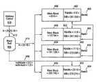
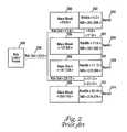
- erase blocks 502are not specific to the memory array bank 504 being addressed by the access in the Flash memory of FIG. 5 , if a memory array bank 504 accumulates defective erase blocks 502 it can be repaired with erase blocks 502 from other memory array banks 504 . This allows the use of erase block replacement schemes that are not constrained by the structure of the memory device or its internal bank structure.
Landscapes
- Engineering & Computer Science (AREA)
- Theoretical Computer Science (AREA)
- Physics & Mathematics (AREA)
- General Engineering & Computer Science (AREA)
- General Physics & Mathematics (AREA)
- For Increasing The Reliability Of Semiconductor Memories (AREA)
- Read Only Memory (AREA)
- Techniques For Improving Reliability Of Storages (AREA)
Abstract
Description
Claims (10)
Priority Applications (3)
| Application Number | Priority Date | Filing Date | Title |
|---|---|---|---|
| US12/387,058US7908427B2 (en) | 2002-07-19 | 2009-04-27 | Non-volatile memory devices and control and operation thereof |
| US13/035,580US8145832B2 (en) | 2002-07-19 | 2011-02-25 | Non-volatile memory devices and control and operation thereof |
| US13/399,587US9213630B2 (en) | 2002-07-19 | 2012-02-17 | Non-volatile memory devices and control and operation thereof |
Applications Claiming Priority (3)
| Application Number | Priority Date | Filing Date | Title |
|---|---|---|---|
| US10/199,725US7123512B2 (en) | 2002-07-19 | 2002-07-19 | Contiguous block addressing scheme |
| US11/581,887US7546440B2 (en) | 2002-07-19 | 2006-10-17 | Non-volatile memory devices and control and operation thereof |
| US12/387,058US7908427B2 (en) | 2002-07-19 | 2009-04-27 | Non-volatile memory devices and control and operation thereof |
Related Parent Applications (1)
| Application Number | Title | Priority Date | Filing Date |
|---|---|---|---|
| US11/581,887ContinuationUS7546440B2 (en) | 2002-07-19 | 2006-10-17 | Non-volatile memory devices and control and operation thereof |
Related Child Applications (1)
| Application Number | Title | Priority Date | Filing Date |
|---|---|---|---|
| US13/035,580ContinuationUS8145832B2 (en) | 2002-07-19 | 2011-02-25 | Non-volatile memory devices and control and operation thereof |
Publications (2)
| Publication Number | Publication Date |
|---|---|
| US20100030949A1 US20100030949A1 (en) | 2010-02-04 |
| US7908427B2true US7908427B2 (en) | 2011-03-15 |
Family
ID=30443390
Family Applications (8)
| Application Number | Title | Priority Date | Filing Date |
|---|---|---|---|
| US10/199,725Expired - LifetimeUS7123512B2 (en) | 2002-07-19 | 2002-07-19 | Contiguous block addressing scheme |
| US11/207,105Expired - LifetimeUS7154782B2 (en) | 2002-07-19 | 2005-08-18 | Contiguous block addressing scheme |
| US11/207,017Expired - LifetimeUS7154781B2 (en) | 2002-07-19 | 2005-08-18 | Contiguous block addressing scheme |
| US11/206,529Expired - LifetimeUS7154780B2 (en) | 2002-07-19 | 2005-08-18 | Contiguous block addressing scheme |
| US11/581,887Expired - LifetimeUS7546440B2 (en) | 2002-07-19 | 2006-10-17 | Non-volatile memory devices and control and operation thereof |
| US12/387,058Expired - Fee RelatedUS7908427B2 (en) | 2002-07-19 | 2009-04-27 | Non-volatile memory devices and control and operation thereof |
| US13/035,580Expired - Fee RelatedUS8145832B2 (en) | 2002-07-19 | 2011-02-25 | Non-volatile memory devices and control and operation thereof |
| US13/399,587Expired - Fee RelatedUS9213630B2 (en) | 2002-07-19 | 2012-02-17 | Non-volatile memory devices and control and operation thereof |
Family Applications Before (5)
| Application Number | Title | Priority Date | Filing Date |
|---|---|---|---|
| US10/199,725Expired - LifetimeUS7123512B2 (en) | 2002-07-19 | 2002-07-19 | Contiguous block addressing scheme |
| US11/207,105Expired - LifetimeUS7154782B2 (en) | 2002-07-19 | 2005-08-18 | Contiguous block addressing scheme |
| US11/207,017Expired - LifetimeUS7154781B2 (en) | 2002-07-19 | 2005-08-18 | Contiguous block addressing scheme |
| US11/206,529Expired - LifetimeUS7154780B2 (en) | 2002-07-19 | 2005-08-18 | Contiguous block addressing scheme |
| US11/581,887Expired - LifetimeUS7546440B2 (en) | 2002-07-19 | 2006-10-17 | Non-volatile memory devices and control and operation thereof |
Family Applications After (2)
| Application Number | Title | Priority Date | Filing Date |
|---|---|---|---|
| US13/035,580Expired - Fee RelatedUS8145832B2 (en) | 2002-07-19 | 2011-02-25 | Non-volatile memory devices and control and operation thereof |
| US13/399,587Expired - Fee RelatedUS9213630B2 (en) | 2002-07-19 | 2012-02-17 | Non-volatile memory devices and control and operation thereof |
Country Status (1)
| Country | Link |
|---|---|
| US (8) | US7123512B2 (en) |
Cited By (1)
| Publication number | Priority date | Publication date | Assignee | Title |
|---|---|---|---|---|
| US20090300277A1 (en)* | 2008-05-27 | 2009-12-03 | Micron Technology, Inc. | Devices and methods for operating a solid state drive |
Families Citing this family (61)
| Publication number | Priority date | Publication date | Assignee | Title |
|---|---|---|---|---|
| US7123512B2 (en)* | 2002-07-19 | 2006-10-17 | Micron Technology, Inc. | Contiguous block addressing scheme |
| JP4218406B2 (en)* | 2003-04-25 | 2009-02-04 | 富士フイルム株式会社 | Information recording and playback method |
| US6906961B2 (en)* | 2003-06-24 | 2005-06-14 | Micron Technology, Inc. | Erase block data splitting |
| US7559004B1 (en)* | 2003-10-01 | 2009-07-07 | Sandisk Corporation | Dynamic redundant area configuration in a non-volatile memory system |
| DE10345978A1 (en)* | 2003-10-02 | 2005-04-28 | Infineon Technologies Ag | Data memory device for computer system, has additional memory banks activated by bank select signals provided by controller-processor unit via control bus |
| JP4284200B2 (en)* | 2004-01-28 | 2009-06-24 | 株式会社東芝 | Nonvolatile semiconductor memory system |
| US7350044B2 (en)* | 2004-01-30 | 2008-03-25 | Micron Technology, Inc. | Data move method and apparatus |
| JP4642018B2 (en)* | 2004-04-21 | 2011-03-02 | スパンション エルエルシー | NONVOLATILE SEMICONDUCTOR DEVICE AND AUTOMATIC REMEDY METHOD FOR ERASE OPERATION OF NONVOLATILE SEMICONDUCTOR DEVICE |
| JP2006107590A (en)* | 2004-10-04 | 2006-04-20 | Nec Electronics Corp | Semiconductor integrated circuit device and its test method |
| US7490197B2 (en) | 2004-10-21 | 2009-02-10 | Microsoft Corporation | Using external memory devices to improve system performance |
| US20060156089A1 (en)* | 2004-12-02 | 2006-07-13 | Chao-Yu Yang | Method and apparatus utilizing defect memories |
| US20060136652A1 (en)* | 2004-12-21 | 2006-06-22 | Via Technologies, Inc. | Electronic system with remap function and method for generating bank with remap function |
| US7405989B2 (en)* | 2005-03-07 | 2008-07-29 | Taiwan Semiconductor Manufacturing Co., Ltd. | Electrical fuses with redundancy |
| US7289363B2 (en)* | 2005-05-19 | 2007-10-30 | Micron Technology, Inc. | Memory cell repair using fuse programming method in a flash memory device |
| US7752381B2 (en) | 2005-05-24 | 2010-07-06 | Micron Technology, Inc. | Version based non-volatile memory translation layer |
| US7509474B2 (en) | 2005-06-08 | 2009-03-24 | Micron Technology, Inc. | Robust index storage for non-volatile memory |
| US7352621B2 (en)* | 2005-06-23 | 2008-04-01 | Intel Corporation | Method for enhanced block management |
| CN100573476C (en)* | 2005-09-25 | 2009-12-23 | 深圳市朗科科技股份有限公司 | Flash media data management method |
| US8914557B2 (en) | 2005-12-16 | 2014-12-16 | Microsoft Corporation | Optimizing write and wear performance for a memory |
| US8429352B2 (en)* | 2007-06-08 | 2013-04-23 | Sandisk Technologies Inc. | Method and system for memory block flushing |
| KR100866626B1 (en)* | 2007-07-02 | 2008-11-03 | 삼성전자주식회사 | Nonvolatile memory device having spare area and block erasing method thereof |
| US20090013148A1 (en) | 2007-07-03 | 2009-01-08 | Micron Technology, Inc. | Block addressing for parallel memory arrays |
| KR20090014823A (en)* | 2007-08-07 | 2009-02-11 | 삼성전자주식회사 | Flash memory device for remapping bad blocks and method of remapping bad blocks thereof |
| US7984329B2 (en)* | 2007-09-04 | 2011-07-19 | International Business Machines Corporation | System and method for providing DRAM device-level repair via address remappings external to the device |
| KR100954913B1 (en)* | 2007-11-29 | 2010-04-27 | 주식회사 동부하이텍 | Manufacturing Method of Flash Memory Device |
| CN101458960B (en)* | 2007-12-13 | 2011-12-07 | 中芯国际集成电路制造(上海)有限公司 | Capacity overlapping memory and control method therefor |
| US20090271562A1 (en)* | 2008-04-25 | 2009-10-29 | Sinclair Alan W | Method and system for storage address re-mapping for a multi-bank memory device |
| US9032151B2 (en) | 2008-09-15 | 2015-05-12 | Microsoft Technology Licensing, Llc | Method and system for ensuring reliability of cache data and metadata subsequent to a reboot |
| US7953774B2 (en) | 2008-09-19 | 2011-05-31 | Microsoft Corporation | Aggregation of write traffic to a data store |
| US8243536B2 (en)* | 2009-09-08 | 2012-08-14 | Lsi Corporation | Systems and methods for increasing bit density in a memory cell |
| US8473669B2 (en)* | 2009-12-07 | 2013-06-25 | Sandisk Technologies Inc. | Method and system for concurrent background and foreground operations in a non-volatile memory array |
| US10360143B2 (en)* | 2010-07-01 | 2019-07-23 | Qualcomm Incorporated | Parallel use of integrated non-volatile memory and main volatile memory within a mobile device |
| US8452911B2 (en) | 2010-09-30 | 2013-05-28 | Sandisk Technologies Inc. | Synchronized maintenance operations in a multi-bank storage system |
| US8762627B2 (en) | 2011-12-21 | 2014-06-24 | Sandisk Technologies Inc. | Memory logical defragmentation during garbage collection |
| CN104040483B (en) | 2011-12-27 | 2017-07-07 | 英特尔公司 | For the cold bootstrap of the optimization of nonvolatile memory |
| US8811060B2 (en) | 2012-05-31 | 2014-08-19 | International Business Machines Corporation | Non-volatile memory crosspoint repair |
| US9026719B2 (en) | 2012-11-15 | 2015-05-05 | Elwha, Llc | Intelligent monitoring for computation in memory |
| US9442854B2 (en) | 2012-11-15 | 2016-09-13 | Elwha Llc | Memory circuitry including computational circuitry for performing supplemental functions |
| US9582465B2 (en)* | 2012-11-15 | 2017-02-28 | Elwha Llc | Flexible processors and flexible memory |
| US9323499B2 (en) | 2012-11-15 | 2016-04-26 | Elwha Llc | Random number generator functions in memory |
| US9734911B2 (en) | 2012-12-31 | 2017-08-15 | Sandisk Technologies Llc | Method and system for asynchronous die operations in a non-volatile memory |
| US9223693B2 (en) | 2012-12-31 | 2015-12-29 | Sandisk Technologies Inc. | Memory system having an unequal number of memory die on different control channels |
| US8873284B2 (en) | 2012-12-31 | 2014-10-28 | Sandisk Technologies Inc. | Method and system for program scheduling in a multi-layer memory |
| US9734050B2 (en) | 2012-12-31 | 2017-08-15 | Sandisk Technologies Llc | Method and system for managing background operations in a multi-layer memory |
| US9348746B2 (en) | 2012-12-31 | 2016-05-24 | Sandisk Technologies | Method and system for managing block reclaim operations in a multi-layer memory |
| US9336133B2 (en) | 2012-12-31 | 2016-05-10 | Sandisk Technologies Inc. | Method and system for managing program cycles including maintenance programming operations in a multi-layer memory |
| US9465731B2 (en) | 2012-12-31 | 2016-10-11 | Sandisk Technologies Llc | Multi-layer non-volatile memory system having multiple partitions in a layer |
| US20150222291A1 (en)* | 2014-02-05 | 2015-08-06 | Kabushiki Kaisha Toshiba | Memory controller, storage device and memory control method |
| TWI525627B (en)* | 2014-03-07 | 2016-03-11 | Toshiba Kk | Semiconductor memory device |
| KR20160042221A (en)* | 2014-10-07 | 2016-04-19 | 에스케이하이닉스 주식회사 | Repair circuit and semiconductor apparatus using the same |
| US9952784B2 (en)* | 2015-03-11 | 2018-04-24 | Sandisk Technologies Llc | Multichip dual write |
| US10042553B2 (en) | 2015-10-30 | 2018-08-07 | Sandisk Technologies Llc | Method and system for programming a multi-layer non-volatile memory having a single fold data path |
| US10133490B2 (en) | 2015-10-30 | 2018-11-20 | Sandisk Technologies Llc | System and method for managing extended maintenance scheduling in a non-volatile memory |
| US10120613B2 (en) | 2015-10-30 | 2018-11-06 | Sandisk Technologies Llc | System and method for rescheduling host and maintenance operations in a non-volatile memory |
| US9778855B2 (en) | 2015-10-30 | 2017-10-03 | Sandisk Technologies Llc | System and method for precision interleaving of data writes in a non-volatile memory |
| KR102420897B1 (en)* | 2016-03-17 | 2022-07-18 | 에스케이하이닉스 주식회사 | Memory module, memory system inculding the same, and operation method thereof |
| US10020067B2 (en) | 2016-08-31 | 2018-07-10 | Nxp Usa, Inc. | Integrated circuits and methods for dynamic allocation of one-time programmable memory |
| US10725933B2 (en)* | 2016-12-30 | 2020-07-28 | Intel Corporation | Method and apparatus for redirecting memory access commands sent to unusable memory partitions |
| IT201700020134A1 (en)* | 2017-02-22 | 2018-08-22 | St Microelectronics Srl | PROCEDURE FOR MANAGING SEMICONDUCTOR MEMORIES, INTERFACE, MEMORY AND CORRESPONDENT DEVICE |
| US11335430B2 (en) | 2019-03-26 | 2022-05-17 | Rambus Inc. | Error remapping |
| CN116137174A (en) | 2021-11-16 | 2023-05-19 | 三星电子株式会社 | Non-volatile memory device and method of operating the same |
Citations (21)
| Publication number | Priority date | Publication date | Assignee | Title |
|---|---|---|---|---|
| JPH03259460A (en) | 1990-03-08 | 1991-11-19 | Fujitsu Ltd | Disk control system |
| US5283790A (en) | 1989-12-25 | 1994-02-01 | Hitachi, Ltd. | External storage apparatus and defective block reassignment processing method therefor |
| US5742934A (en) | 1995-09-13 | 1998-04-21 | Mitsubishi Denki Kabushiki Kaisha | Flash solid state disk card with selective use of an address conversion table depending on logical and physical sector numbers |
| US5925138A (en) | 1997-03-04 | 1999-07-20 | Micron Electronics, Inc. | Method for allowing data transfers with a memory having defective storage locations |
| US5974544A (en) | 1991-12-17 | 1999-10-26 | Dell Usa, L.P. | Method and controller for defect tracking in a redundant array |
| US6021459A (en) | 1997-04-23 | 2000-02-01 | Micron Technology, Inc. | Memory system having flexible bus structure and method |
| US6034891A (en) | 1997-12-01 | 2000-03-07 | Micron Technology, Inc. | Multi-state flash memory defect management |
| US6055611A (en) | 1997-07-09 | 2000-04-25 | Micron Technology, Inc. | Method and apparatus for enabling redundant memory |
| US6081463A (en) | 1998-02-25 | 2000-06-27 | Micron Technology, Inc. | Semiconductor memory remapping |
| US6084807A (en) | 1999-11-08 | 2000-07-04 | Choi; Jin H. | Memory device with global redundancy |
| US6175891B1 (en) | 1997-04-23 | 2001-01-16 | Micron Technology, Inc. | System and method for assigning addresses to memory devices |
| US6246615B1 (en) | 1998-12-23 | 2001-06-12 | Micron Technology, Inc. | Redundancy mapping in a multichip semiconductor package |
| US20020012282A1 (en) | 1999-06-03 | 2002-01-31 | Hidetoshi Saito | Semiconductor memory and nonvolatile semiconductor memory having redundant circuitry for replacing defective memory cell |
| US20020027264A1 (en) | 1999-08-26 | 2002-03-07 | Micron Technology, Inc. | MOSFET technology for programmable address decode and correction |
| US20020157048A1 (en) | 2001-04-19 | 2002-10-24 | Micron Technology, Inc. | Memory with element redundancy |
| US6504768B1 (en) | 2000-08-25 | 2003-01-07 | Micron Technology, Inc. | Redundancy selection in memory devices with concurrent read and write |
| US6507885B2 (en) | 1996-10-29 | 2003-01-14 | Micron Technology, Inc. | Memory system, method and predecoding circuit operable in different modes for selectively accessing multiple blocks of memory cells for simultaneous writing or erasure |
| US20030031052A1 (en) | 2001-08-13 | 2003-02-13 | Micron Technology, Inc. | Synchronous flash memory with virtual segment architecture |
| US6671775B2 (en) | 1998-11-20 | 2003-12-30 | Lg Electronics Inc. | Spare area management method of optical recording medium |
| US6766409B2 (en) | 1993-10-01 | 2004-07-20 | Fujitsu Limited | Method of writing, erasing, and controlling memory for memory device |
| US7123512B2 (en) | 2002-07-19 | 2006-10-17 | Micron Technology, Inc. | Contiguous block addressing scheme |
Family Cites Families (7)
| Publication number | Priority date | Publication date | Assignee | Title |
|---|---|---|---|---|
| US4346459A (en)* | 1980-06-30 | 1982-08-24 | Inmos Corporation | Redundancy scheme for an MOS memory |
| US4493075A (en)* | 1982-05-17 | 1985-01-08 | National Semiconductor Corporation | Self repairing bulk memory |
| US6035432A (en)* | 1997-07-31 | 2000-03-07 | Micron Electronics, Inc. | System for remapping defective memory bit sets |
| KR100363085B1 (en)* | 1999-11-05 | 2002-12-05 | 삼성전자 주식회사 | Semiconductor memory device having row redundancy scheme for improving redundancy efficiency |
| JP2002319296A (en)* | 2001-04-19 | 2002-10-31 | Nec Corp | Semiconductor device, system and method |
| US20030028834A1 (en)* | 2001-08-01 | 2003-02-06 | Brown David R. | Method for sharing redundant rows between banks for improved repair efficiency |
| JP2004095001A (en)* | 2002-08-29 | 2004-03-25 | Fujitsu Ltd | Nonvolatile semiconductor memory device, nonvolatile semiconductor memory device embedded system, and defective block detection method |
- 2002
- 2002-07-19USUS10/199,725patent/US7123512B2/ennot_activeExpired - Lifetime
- 2005
- 2005-08-18USUS11/207,105patent/US7154782B2/ennot_activeExpired - Lifetime
- 2005-08-18USUS11/207,017patent/US7154781B2/ennot_activeExpired - Lifetime
- 2005-08-18USUS11/206,529patent/US7154780B2/ennot_activeExpired - Lifetime
- 2006
- 2006-10-17USUS11/581,887patent/US7546440B2/ennot_activeExpired - Lifetime
- 2009
- 2009-04-27USUS12/387,058patent/US7908427B2/ennot_activeExpired - Fee Related
- 2011
- 2011-02-25USUS13/035,580patent/US8145832B2/ennot_activeExpired - Fee Related
- 2012
- 2012-02-17USUS13/399,587patent/US9213630B2/ennot_activeExpired - Fee Related
Patent Citations (25)
| Publication number | Priority date | Publication date | Assignee | Title |
|---|---|---|---|---|
| US5283790A (en) | 1989-12-25 | 1994-02-01 | Hitachi, Ltd. | External storage apparatus and defective block reassignment processing method therefor |
| JPH03259460A (en) | 1990-03-08 | 1991-11-19 | Fujitsu Ltd | Disk control system |
| US5974544A (en) | 1991-12-17 | 1999-10-26 | Dell Usa, L.P. | Method and controller for defect tracking in a redundant array |
| US6766409B2 (en) | 1993-10-01 | 2004-07-20 | Fujitsu Limited | Method of writing, erasing, and controlling memory for memory device |
| US5742934A (en) | 1995-09-13 | 1998-04-21 | Mitsubishi Denki Kabushiki Kaisha | Flash solid state disk card with selective use of an address conversion table depending on logical and physical sector numbers |
| US6507885B2 (en) | 1996-10-29 | 2003-01-14 | Micron Technology, Inc. | Memory system, method and predecoding circuit operable in different modes for selectively accessing multiple blocks of memory cells for simultaneous writing or erasure |
| US5925138A (en) | 1997-03-04 | 1999-07-20 | Micron Electronics, Inc. | Method for allowing data transfers with a memory having defective storage locations |
| US20010003837A1 (en) | 1997-04-23 | 2001-06-14 | Micron Technology, Inc. | Memory system having serial selection of memory devices and method |
| US6175891B1 (en) | 1997-04-23 | 2001-01-16 | Micron Technology, Inc. | System and method for assigning addresses to memory devices |
| US6021459A (en) | 1997-04-23 | 2000-02-01 | Micron Technology, Inc. | Memory system having flexible bus structure and method |
| US6055611A (en) | 1997-07-09 | 2000-04-25 | Micron Technology, Inc. | Method and apparatus for enabling redundant memory |
| US6034891A (en) | 1997-12-01 | 2000-03-07 | Micron Technology, Inc. | Multi-state flash memory defect management |
| US6081463A (en) | 1998-02-25 | 2000-06-27 | Micron Technology, Inc. | Semiconductor memory remapping |
| US6671775B2 (en) | 1998-11-20 | 2003-12-30 | Lg Electronics Inc. | Spare area management method of optical recording medium |
| US6246615B1 (en) | 1998-12-23 | 2001-06-12 | Micron Technology, Inc. | Redundancy mapping in a multichip semiconductor package |
| US20010030897A1 (en) | 1998-12-23 | 2001-10-18 | Micron Technology, Inc. | Redundancy mapping in a multichip semiconductor package |
| US20020012282A1 (en) | 1999-06-03 | 2002-01-31 | Hidetoshi Saito | Semiconductor memory and nonvolatile semiconductor memory having redundant circuitry for replacing defective memory cell |
| US20020027264A1 (en) | 1999-08-26 | 2002-03-07 | Micron Technology, Inc. | MOSFET technology for programmable address decode and correction |
| US6084807A (en) | 1999-11-08 | 2000-07-04 | Choi; Jin H. | Memory device with global redundancy |
| US6504768B1 (en) | 2000-08-25 | 2003-01-07 | Micron Technology, Inc. | Redundancy selection in memory devices with concurrent read and write |
| US20020157048A1 (en) | 2001-04-19 | 2002-10-24 | Micron Technology, Inc. | Memory with element redundancy |
| US6625081B2 (en) | 2001-08-13 | 2003-09-23 | Micron Technology, Inc. | Synchronous flash memory with virtual segment architecture |
| US20030031052A1 (en) | 2001-08-13 | 2003-02-13 | Micron Technology, Inc. | Synchronous flash memory with virtual segment architecture |
| US7123512B2 (en) | 2002-07-19 | 2006-10-17 | Micron Technology, Inc. | Contiguous block addressing scheme |
| US20070038800A1 (en) | 2002-07-19 | 2007-02-15 | Micron Technology, Inc. | Contiguous block addressing scheme |
Cited By (2)
| Publication number | Priority date | Publication date | Assignee | Title |
|---|---|---|---|---|
| US20090300277A1 (en)* | 2008-05-27 | 2009-12-03 | Micron Technology, Inc. | Devices and methods for operating a solid state drive |
| US8554983B2 (en)* | 2008-05-27 | 2013-10-08 | Micron Technology, Inc. | Devices and methods for operating a solid state drive |
Also Published As
| Publication number | Publication date |
|---|---|
| US20070038800A1 (en) | 2007-02-15 |
| US20110238894A1 (en) | 2011-09-29 |
| US8145832B2 (en) | 2012-03-27 |
| US7123512B2 (en) | 2006-10-17 |
| US7154781B2 (en) | 2006-12-26 |
| US20100030949A1 (en) | 2010-02-04 |
| US7154780B2 (en) | 2006-12-26 |
| US20120215967A1 (en) | 2012-08-23 |
| US9213630B2 (en) | 2015-12-15 |
| US20050278481A1 (en) | 2005-12-15 |
| US7154782B2 (en) | 2006-12-26 |
| US20050276121A1 (en) | 2005-12-15 |
| US20040015674A1 (en) | 2004-01-22 |
| US7546440B2 (en) | 2009-06-09 |
| US20050276130A1 (en) | 2005-12-15 |
Similar Documents
| Publication | Publication Date | Title |
|---|---|---|
| US7908427B2 (en) | Non-volatile memory devices and control and operation thereof | |
| KR100622349B1 (en) | A method for managing a defective block in a flash memory device and a flash memory device having a defective block management function. | |
| US7743303B2 (en) | Defective memory block remapping method and system, and memory device and processor-based system using same | |
| US7472331B2 (en) | Memory systems including defective block management and related methods | |
| US7571362B2 (en) | Method of managing fails in a non-volatile memory device and relative memory device | |
| KR101535460B1 (en) | Nonvolatile memory device having bad block remapping function and bad block remapping method thereof | |
| US7366946B2 (en) | ROM redundancy in ROM embedded DRAM | |
| US20120075943A1 (en) | Method and Apparatus for Memory Repair With Redundant Columns | |
| US8743650B2 (en) | Block repair scheme | |
| KR20090014823A (en) | Flash memory device for remapping bad blocks and method of remapping bad blocks thereof | |
| JPH1027499A (en) | Nonvolatile memory device having divided redundancy to be electrically erased/programmed | |
| JP4034947B2 (en) | Nonvolatile storage system | |
| US20080052445A1 (en) | Flash memory devices including block information blocks and methods of operating same | |
| US7154803B2 (en) | Redundancy scheme for a memory integrated circuit | |
| JP4433792B2 (en) | MEMORY CONTROLLER, FLASH MEMORY SYSTEM PROVIDED WITH MEMORY CONTROLLER, AND FLASH MEMORY CONTROL METHOD | |
| JP4641034B2 (en) | Nonvolatile storage system | |
| JP2011048852A (en) | Nonvolatile memory system |
Legal Events
| Date | Code | Title | Description |
|---|---|---|---|
| AS | Assignment | Owner name:MOSAID TECHNOLOGIES INCORPORATED,CANADA Free format text:ASSIGNMENT OF ASSIGNORS INTEREST;ASSIGNOR:MICRON TECHNOLOGY, INC.;REEL/FRAME:023404/0336 Effective date:20090402 Owner name:MOSAID TECHNOLOGIES INCORPORATED, CANADA Free format text:ASSIGNMENT OF ASSIGNORS INTEREST;ASSIGNOR:MICRON TECHNOLOGY, INC.;REEL/FRAME:023404/0336 Effective date:20090402 | |
| AS | Assignment | Owner name:MICRON TECHNOLOGY, INC.,IDAHO Free format text:ASSIGNMENT OF ASSIGNORS INTEREST;ASSIGNORS:LAKHANI, VINOD;LOUIE, BENJAMIN;REEL/FRAME:023507/0210 Effective date:20020627 Owner name:MICRON TECHNOLOGY, INC., IDAHO Free format text:ASSIGNMENT OF ASSIGNORS INTEREST;ASSIGNORS:LAKHANI, VINOD;LOUIE, BENJAMIN;REEL/FRAME:023507/0210 Effective date:20020627 | |
| AS | Assignment | Owner name:MOSAID TECHNOLOGIES INCORPORATED,CANADA Free format text:ASSIGNMENT OF ASSIGNORS INTEREST;ASSIGNOR:MICRON TECHNOLOGY INC.;REEL/FRAME:023627/0576 Effective date:20090402 Owner name:MOSAID TECHNOLOGIES INCORPORATED, CANADA Free format text:ASSIGNMENT OF ASSIGNORS INTEREST;ASSIGNOR:MICRON TECHNOLOGY INC.;REEL/FRAME:023627/0576 Effective date:20090402 | |
| FEPP | Fee payment procedure | Free format text:PAYOR NUMBER ASSIGNED (ORIGINAL EVENT CODE: ASPN); ENTITY STATUS OF PATENT OWNER: LARGE ENTITY | |
| STCF | Information on status: patent grant | Free format text:PATENTED CASE | |
| AS | Assignment | Owner name:ROYAL BANK OF CANADA, CANADA Free format text:U.S. INTELLECTUAL PROPERTY SECURITY AGREEMENT (FOR NON-U.S. GRANTORS) - SHORT FORM;ASSIGNORS:658276 N.B. LTD.;658868 N.B. INC.;MOSAID TECHNOLOGIES INCORPORATED;REEL/FRAME:027512/0196 Effective date:20111223 | |
| AS | Assignment | Owner name:CONVERSANT INTELLECTUAL PROPERTY MANAGEMENT INC., Free format text:CHANGE OF NAME;ASSIGNOR:MOSAID TECHNOLOGIES INCORPORATED;REEL/FRAME:032439/0638 Effective date:20140101 | |
| AS | Assignment | Owner name:CONVERSANT INTELLECTUAL PROPERTY MANAGEMENT INC., Free format text:RELEASE OF SECURITY INTEREST;ASSIGNOR:ROYAL BANK OF CANADA;REEL/FRAME:033484/0344 Effective date:20140611 Owner name:CONVERSANT IP N.B. 276 INC., CANADA Free format text:RELEASE OF SECURITY INTEREST;ASSIGNOR:ROYAL BANK OF CANADA;REEL/FRAME:033484/0344 Effective date:20140611 Owner name:CONVERSANT IP N.B. 868 INC., CANADA Free format text:RELEASE OF SECURITY INTEREST;ASSIGNOR:ROYAL BANK OF CANADA;REEL/FRAME:033484/0344 Effective date:20140611 | |
| FPAY | Fee payment | Year of fee payment:4 | |
| AS | Assignment | Owner name:CONVERSANT INTELLECTUAL PROPERTY MANAGEMENT INC., CANADA Free format text:CHANGE OF ADDRESS;ASSIGNOR:CONVERSANT INTELLECTUAL PROPERTY MANAGEMENT INC.;REEL/FRAME:033678/0096 Effective date:20140820 Owner name:CONVERSANT INTELLECTUAL PROPERTY MANAGEMENT INC., Free format text:CHANGE OF ADDRESS;ASSIGNOR:CONVERSANT INTELLECTUAL PROPERTY MANAGEMENT INC.;REEL/FRAME:033678/0096 Effective date:20140820 | |
| AS | Assignment | Owner name:CPPIB CREDIT INVESTMENTS INC., AS LENDER, CANADA Free format text:U.S. PATENT SECURITY AGREEMENT (FOR NON-U.S. GRANTORS);ASSIGNOR:CONVERSANT INTELLECTUAL PROPERTY MANAGEMENT INC.;REEL/FRAME:033706/0367 Effective date:20140611 Owner name:ROYAL BANK OF CANADA, AS LENDER, CANADA Free format text:U.S. PATENT SECURITY AGREEMENT (FOR NON-U.S. GRANTORS);ASSIGNOR:CONVERSANT INTELLECTUAL PROPERTY MANAGEMENT INC.;REEL/FRAME:033706/0367 Effective date:20140611 | |
| AS | Assignment | Owner name:CPPIB CREDIT INVESTMENTS, INC., CANADA Free format text:AMENDED AND RESTATED U.S. PATENT SECURITY AGREEMENT (FOR NON-U.S. GRANTORS);ASSIGNOR:CONVERSANT INTELLECTUAL PROPERTY MANAGEMENT INC.;REEL/FRAME:046900/0136 Effective date:20180731 | |
| MAFP | Maintenance fee payment | Free format text:PAYMENT OF MAINTENANCE FEE, 8TH YEAR, LARGE ENTITY (ORIGINAL EVENT CODE: M1552); ENTITY STATUS OF PATENT OWNER: LARGE ENTITY Year of fee payment:8 | |
| AS | Assignment | Owner name:CONVERSANT INTELLECTUAL PROPERTY MANAGEMENT INC., CANADA Free format text:RELEASE OF U.S. PATENT AGREEMENT (FOR NON-U.S. GRANTORS);ASSIGNOR:ROYAL BANK OF CANADA, AS LENDER;REEL/FRAME:047645/0424 Effective date:20180731 Owner name:CONVERSANT INTELLECTUAL PROPERTY MANAGEMENT INC., Free format text:RELEASE OF U.S. PATENT AGREEMENT (FOR NON-U.S. GRANTORS);ASSIGNOR:ROYAL BANK OF CANADA, AS LENDER;REEL/FRAME:047645/0424 Effective date:20180731 | |
| AS | Assignment | Owner name:CONVERSANT INTELLECTUAL PROPERTY MANAGEMENT INC., CANADA Free format text:RELEASE BY SECURED PARTY;ASSIGNOR:CPPIB CREDIT INVESTMENTS INC.;REEL/FRAME:054372/0194 Effective date:20201028 | |
| AS | Assignment | Owner name:MOSAID TECHNOLOGIES INCORPORATED, CANADA Free format text:CHANGE OF NAME;ASSIGNOR:CONVERSANT INTELLECTUAL PROPERTY MANAGEMENT INC.;REEL/FRAME:057709/0853 Effective date:20210401 | |
| FEPP | Fee payment procedure | Free format text:MAINTENANCE FEE REMINDER MAILED (ORIGINAL EVENT CODE: REM.); ENTITY STATUS OF PATENT OWNER: LARGE ENTITY | |
| LAPS | Lapse for failure to pay maintenance fees | Free format text:PATENT EXPIRED FOR FAILURE TO PAY MAINTENANCE FEES (ORIGINAL EVENT CODE: EXP.); ENTITY STATUS OF PATENT OWNER: LARGE ENTITY | |
| STCH | Information on status: patent discontinuation | Free format text:PATENT EXPIRED DUE TO NONPAYMENT OF MAINTENANCE FEES UNDER 37 CFR 1.362 | |
| FP | Lapsed due to failure to pay maintenance fee | Effective date:20230315 |