US7906845B1 - Semiconductor device having reduced thermal interface material (TIM) degradation and method therefor - Google Patents
Semiconductor device having reduced thermal interface material (TIM) degradation and method thereforDownload PDFInfo
- Publication number
- US7906845B1 US7906845B1US12/108,419US10841908AUS7906845B1US 7906845 B1US7906845 B1US 7906845B1US 10841908 AUS10841908 AUS 10841908AUS 7906845 B1US7906845 B1US 7906845B1
- Authority
- US
- United States
- Prior art keywords
- lid member
- top surface
- substrate
- semiconductor device
- die
- Prior art date
- Legal status (The legal status is an assumption and is not a legal conclusion. Google has not performed a legal analysis and makes no representation as to the accuracy of the status listed.)
- Active, expires
Links
Images


Classifications
- H—ELECTRICITY
- H01—ELECTRIC ELEMENTS
- H01L—SEMICONDUCTOR DEVICES NOT COVERED BY CLASS H10
- H01L23/00—Details of semiconductor or other solid state devices
- H01L23/02—Containers; Seals
- H01L23/04—Containers; Seals characterised by the shape of the container or parts, e.g. caps, walls
- H—ELECTRICITY
- H01—ELECTRIC ELEMENTS
- H01L—SEMICONDUCTOR DEVICES NOT COVERED BY CLASS H10
- H01L23/00—Details of semiconductor or other solid state devices
- H01L23/34—Arrangements for cooling, heating, ventilating or temperature compensation ; Temperature sensing arrangements
- H01L23/42—Fillings or auxiliary members in containers or encapsulations selected or arranged to facilitate heating or cooling
- H—ELECTRICITY
- H01—ELECTRIC ELEMENTS
- H01L—SEMICONDUCTOR DEVICES NOT COVERED BY CLASS H10
- H01L23/00—Details of semiconductor or other solid state devices
- H01L23/562—Protection against mechanical damage
- H—ELECTRICITY
- H01—ELECTRIC ELEMENTS
- H01L—SEMICONDUCTOR DEVICES NOT COVERED BY CLASS H10
- H01L2224/00—Indexing scheme for arrangements for connecting or disconnecting semiconductor or solid-state bodies and methods related thereto as covered by H01L24/00
- H01L2224/01—Means for bonding being attached to, or being formed on, the surface to be connected, e.g. chip-to-package, die-attach, "first-level" interconnects; Manufacturing methods related thereto
- H01L2224/10—Bump connectors; Manufacturing methods related thereto
- H01L2224/15—Structure, shape, material or disposition of the bump connectors after the connecting process
- H01L2224/16—Structure, shape, material or disposition of the bump connectors after the connecting process of an individual bump connector
- H01L2224/161—Disposition
- H01L2224/16151—Disposition the bump connector connecting between a semiconductor or solid-state body and an item not being a semiconductor or solid-state body, e.g. chip-to-substrate, chip-to-passive
- H01L2224/16221—Disposition the bump connector connecting between a semiconductor or solid-state body and an item not being a semiconductor or solid-state body, e.g. chip-to-substrate, chip-to-passive the body and the item being stacked
- H01L2224/16225—Disposition the bump connector connecting between a semiconductor or solid-state body and an item not being a semiconductor or solid-state body, e.g. chip-to-substrate, chip-to-passive the body and the item being stacked the item being non-metallic, e.g. insulating substrate with or without metallisation
- H—ELECTRICITY
- H01—ELECTRIC ELEMENTS
- H01L—SEMICONDUCTOR DEVICES NOT COVERED BY CLASS H10
- H01L2224/00—Indexing scheme for arrangements for connecting or disconnecting semiconductor or solid-state bodies and methods related thereto as covered by H01L24/00
- H01L2224/01—Means for bonding being attached to, or being formed on, the surface to be connected, e.g. chip-to-package, die-attach, "first-level" interconnects; Manufacturing methods related thereto
- H01L2224/26—Layer connectors, e.g. plate connectors, solder or adhesive layers; Manufacturing methods related thereto
- H01L2224/31—Structure, shape, material or disposition of the layer connectors after the connecting process
- H01L2224/32—Structure, shape, material or disposition of the layer connectors after the connecting process of an individual layer connector
- H01L2224/321—Disposition
- H01L2224/32151—Disposition the layer connector connecting between a semiconductor or solid-state body and an item not being a semiconductor or solid-state body, e.g. chip-to-substrate, chip-to-passive
- H01L2224/32221—Disposition the layer connector connecting between a semiconductor or solid-state body and an item not being a semiconductor or solid-state body, e.g. chip-to-substrate, chip-to-passive the body and the item being stacked
- H01L2224/32225—Disposition the layer connector connecting between a semiconductor or solid-state body and an item not being a semiconductor or solid-state body, e.g. chip-to-substrate, chip-to-passive the body and the item being stacked the item being non-metallic, e.g. insulating substrate with or without metallisation
- H—ELECTRICITY
- H01—ELECTRIC ELEMENTS
- H01L—SEMICONDUCTOR DEVICES NOT COVERED BY CLASS H10
- H01L2224/00—Indexing scheme for arrangements for connecting or disconnecting semiconductor or solid-state bodies and methods related thereto as covered by H01L24/00
- H01L2224/73—Means for bonding being of different types provided for in two or more of groups H01L2224/10, H01L2224/18, H01L2224/26, H01L2224/34, H01L2224/42, H01L2224/50, H01L2224/63, H01L2224/71
- H01L2224/732—Location after the connecting process
- H01L2224/73201—Location after the connecting process on the same surface
- H01L2224/73203—Bump and layer connectors
- H01L2224/73204—Bump and layer connectors the bump connector being embedded into the layer connector
- H—ELECTRICITY
- H01—ELECTRIC ELEMENTS
- H01L—SEMICONDUCTOR DEVICES NOT COVERED BY CLASS H10
- H01L2224/00—Indexing scheme for arrangements for connecting or disconnecting semiconductor or solid-state bodies and methods related thereto as covered by H01L24/00
- H01L2224/73—Means for bonding being of different types provided for in two or more of groups H01L2224/10, H01L2224/18, H01L2224/26, H01L2224/34, H01L2224/42, H01L2224/50, H01L2224/63, H01L2224/71
- H01L2224/732—Location after the connecting process
- H01L2224/73251—Location after the connecting process on different surfaces
- H01L2224/73253—Bump and layer connectors
- H—ELECTRICITY
- H01—ELECTRIC ELEMENTS
- H01L—SEMICONDUCTOR DEVICES NOT COVERED BY CLASS H10
- H01L23/00—Details of semiconductor or other solid state devices
- H01L23/02—Containers; Seals
- H01L23/10—Containers; Seals characterised by the material or arrangement of seals between parts, e.g. between cap and base of the container or between leads and walls of the container
- H—ELECTRICITY
- H01—ELECTRIC ELEMENTS
- H01L—SEMICONDUCTOR DEVICES NOT COVERED BY CLASS H10
- H01L25/00—Assemblies consisting of a plurality of semiconductor or other solid state devices
- H01L25/03—Assemblies consisting of a plurality of semiconductor or other solid state devices all the devices being of a type provided for in a single subclass of subclasses H10B, H10D, H10F, H10H, H10K or H10N, e.g. assemblies of rectifier diodes
- H01L25/04—Assemblies consisting of a plurality of semiconductor or other solid state devices all the devices being of a type provided for in a single subclass of subclasses H10B, H10D, H10F, H10H, H10K or H10N, e.g. assemblies of rectifier diodes the devices not having separate containers
- H01L25/065—Assemblies consisting of a plurality of semiconductor or other solid state devices all the devices being of a type provided for in a single subclass of subclasses H10B, H10D, H10F, H10H, H10K or H10N, e.g. assemblies of rectifier diodes the devices not having separate containers the devices being of a type provided for in group H10D89/00
- H01L25/0655—Assemblies consisting of a plurality of semiconductor or other solid state devices all the devices being of a type provided for in a single subclass of subclasses H10B, H10D, H10F, H10H, H10K or H10N, e.g. assemblies of rectifier diodes the devices not having separate containers the devices being of a type provided for in group H10D89/00 the devices being arranged next to each other
- H—ELECTRICITY
- H01—ELECTRIC ELEMENTS
- H01L—SEMICONDUCTOR DEVICES NOT COVERED BY CLASS H10
- H01L2924/00—Indexing scheme for arrangements or methods for connecting or disconnecting semiconductor or solid-state bodies as covered by H01L24/00
- H01L2924/15—Details of package parts other than the semiconductor or other solid state devices to be connected
- H01L2924/151—Die mounting substrate
- H01L2924/153—Connection portion
- H01L2924/1531—Connection portion the connection portion being formed only on the surface of the substrate opposite to the die mounting surface
- H01L2924/15311—Connection portion the connection portion being formed only on the surface of the substrate opposite to the die mounting surface being a ball array, e.g. BGA
- H—ELECTRICITY
- H01—ELECTRIC ELEMENTS
- H01L—SEMICONDUCTOR DEVICES NOT COVERED BY CLASS H10
- H01L2924/00—Indexing scheme for arrangements or methods for connecting or disconnecting semiconductor or solid-state bodies as covered by H01L24/00
- H01L2924/15—Details of package parts other than the semiconductor or other solid state devices to be connected
- H01L2924/161—Cap
- H01L2924/162—Disposition
- H01L2924/16251—Connecting to an item not being a semiconductor or solid-state body, e.g. cap-to-substrate
Definitions
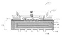
- FIG. 1is a cross-sectional view of a semiconductor device according to a one embodiment of the present invention
Landscapes
- Physics & Mathematics (AREA)
- Condensed Matter Physics & Semiconductors (AREA)
- General Physics & Mathematics (AREA)
- Engineering & Computer Science (AREA)
- Computer Hardware Design (AREA)
- Microelectronics & Electronic Packaging (AREA)
- Power Engineering (AREA)
- Cooling Or The Like Of Semiconductors Or Solid State Devices (AREA)
Abstract
Description
Claims (20)
Priority Applications (1)
| Application Number | Priority Date | Filing Date | Title |
|---|---|---|---|
| US12/108,419US7906845B1 (en) | 2008-04-23 | 2008-04-23 | Semiconductor device having reduced thermal interface material (TIM) degradation and method therefor |
Applications Claiming Priority (1)
| Application Number | Priority Date | Filing Date | Title |
|---|---|---|---|
| US12/108,419US7906845B1 (en) | 2008-04-23 | 2008-04-23 | Semiconductor device having reduced thermal interface material (TIM) degradation and method therefor |
Publications (1)
| Publication Number | Publication Date |
|---|---|
| US7906845B1true US7906845B1 (en) | 2011-03-15 |
Family
ID=43708141
Family Applications (1)
| Application Number | Title | Priority Date | Filing Date |
|---|---|---|---|
| US12/108,419Active2028-10-01US7906845B1 (en) | 2008-04-23 | 2008-04-23 | Semiconductor device having reduced thermal interface material (TIM) degradation and method therefor |
Country Status (1)
| Country | Link |
|---|---|
| US (1) | US7906845B1 (en) |
Cited By (10)
| Publication number | Priority date | Publication date | Assignee | Title |
|---|---|---|---|---|
| US20130083501A1 (en)* | 2011-09-30 | 2013-04-04 | Stmicroelectronics Ltd (Malta) | Method for soldering a cap to a support layer |
| US20160351467A1 (en)* | 2015-05-28 | 2016-12-01 | International Business Machines Corporation | Limiting electronic package warpage |
| US20180019213A1 (en)* | 2015-03-11 | 2018-01-18 | Intel Corporation | Stretchable electronics fabrication method with strain redistribution layer |
| US20190035713A1 (en)* | 2017-07-28 | 2019-01-31 | Qualcomm Incorporated | Systems and methods for cooling an electronic device |
| USD879046S1 (en) | 2017-10-06 | 2020-03-24 | Laird Technologies, Inc. | Material having edging |
| USD881822S1 (en) | 2017-10-06 | 2020-04-21 | Laird Technologies, Inc. | Material having an edge shape |
| US10741519B2 (en) | 2016-07-11 | 2020-08-11 | Laird Technologies, Inc. | Systems of applying materials to components |
| US11014203B2 (en) | 2016-07-11 | 2021-05-25 | Laird Technologies, Inc. | System for applying interface materials |
| US11141823B2 (en) | 2018-04-28 | 2021-10-12 | Laird Technologies, Inc. | Systems and methods of applying materials to components |
| USD999405S1 (en) | 2017-10-06 | 2023-09-19 | Laird Technologies, Inc. | Material having edging |
Citations (18)
| Publication number | Priority date | Publication date | Assignee | Title |
|---|---|---|---|---|
| US3337678A (en) | 1965-06-30 | 1967-08-22 | John P Stelmak | Sealed microminiature electronic package |
| US3422320A (en) | 1965-12-23 | 1969-01-14 | Gen Motors Corp | Sealing technique for composite ferrous-copper base alloy capsules for semiconductor devices |
| US3504096A (en) | 1968-01-31 | 1970-03-31 | Westinghouse Electric Corp | Semiconductor device and method |
| US3538597A (en) | 1967-07-13 | 1970-11-10 | Us Navy | Flatpack lid and method |
| US4577056A (en) | 1984-04-09 | 1986-03-18 | Olin Corporation | Hermetically sealed metal package |
| US5268533A (en) | 1991-05-03 | 1993-12-07 | Hughes Aircraft Company | Pre-stressed laminated lid for electronic circuit package |
| JPH0653341A (en) | 1992-08-03 | 1994-02-25 | Mitsubishi Materials Corp | Clad cap for semiconductor device |
| US5469329A (en) | 1994-08-08 | 1995-11-21 | Ford Motor Company | Printed circuit board with bi-metallic heat spreader |
| US6429512B1 (en) | 1999-03-16 | 2002-08-06 | Siliconware Precision Industries Co., Ltd. | Ball grid array integrated circuit package with palladium coated heat-dissipation device |
| US6462410B1 (en)* | 2000-08-17 | 2002-10-08 | Sun Microsystems Inc | Integrated circuit component temperature gradient reducer |
| US6504242B1 (en) | 2001-11-15 | 2003-01-07 | Intel Corporation | Electronic assembly having a wetting layer on a thermally conductive heat spreader |
| US20030080411A1 (en)* | 2001-10-25 | 2003-05-01 | Samsung Electronics Co., Ltd | Semiconductor package having thermal interface material (TIM) |
| US6611054B1 (en) | 1993-12-22 | 2003-08-26 | Honeywell Inc. | IC package lid for dose enhancement protection |
| US6751099B2 (en)* | 2001-12-20 | 2004-06-15 | Intel Corporation | Coated heat spreaders |
| US6921970B2 (en) | 2001-11-12 | 2005-07-26 | Neomax Materials Co., Ltd. | Package for electronic parts, lid thereof, material for the lid and method for producing the lid material |
| US20050280142A1 (en) | 2004-06-18 | 2005-12-22 | Intel Corporation | Electronic assembly having an indium wetting layer on a thermally conductive body |
| US7173331B2 (en) | 2003-02-06 | 2007-02-06 | Neomax Materials Co., Ltd. | Hermetic sealing cap and method of manufacturing the same |
| US7223638B2 (en) | 2004-05-13 | 2007-05-29 | Intel Corporation | Microelectronic assembly having a thermally conductive member with a cavity to contain a portion of a thermal interface material |
- 2008
- 2008-04-23USUS12/108,419patent/US7906845B1/enactiveActive
Patent Citations (19)
| Publication number | Priority date | Publication date | Assignee | Title |
|---|---|---|---|---|
| US3337678A (en) | 1965-06-30 | 1967-08-22 | John P Stelmak | Sealed microminiature electronic package |
| US3422320A (en) | 1965-12-23 | 1969-01-14 | Gen Motors Corp | Sealing technique for composite ferrous-copper base alloy capsules for semiconductor devices |
| US3538597A (en) | 1967-07-13 | 1970-11-10 | Us Navy | Flatpack lid and method |
| US3504096A (en) | 1968-01-31 | 1970-03-31 | Westinghouse Electric Corp | Semiconductor device and method |
| US4577056A (en) | 1984-04-09 | 1986-03-18 | Olin Corporation | Hermetically sealed metal package |
| US5268533A (en) | 1991-05-03 | 1993-12-07 | Hughes Aircraft Company | Pre-stressed laminated lid for electronic circuit package |
| JPH0653341A (en) | 1992-08-03 | 1994-02-25 | Mitsubishi Materials Corp | Clad cap for semiconductor device |
| US6611054B1 (en) | 1993-12-22 | 2003-08-26 | Honeywell Inc. | IC package lid for dose enhancement protection |
| US5469329A (en) | 1994-08-08 | 1995-11-21 | Ford Motor Company | Printed circuit board with bi-metallic heat spreader |
| US6429512B1 (en) | 1999-03-16 | 2002-08-06 | Siliconware Precision Industries Co., Ltd. | Ball grid array integrated circuit package with palladium coated heat-dissipation device |
| US6462410B1 (en)* | 2000-08-17 | 2002-10-08 | Sun Microsystems Inc | Integrated circuit component temperature gradient reducer |
| US20030080411A1 (en)* | 2001-10-25 | 2003-05-01 | Samsung Electronics Co., Ltd | Semiconductor package having thermal interface material (TIM) |
| US7081375B2 (en) | 2001-10-25 | 2006-07-25 | Samsung Electronics Co., Ltd. | Semiconductor package having thermal interface material (TIM) |
| US6921970B2 (en) | 2001-11-12 | 2005-07-26 | Neomax Materials Co., Ltd. | Package for electronic parts, lid thereof, material for the lid and method for producing the lid material |
| US6504242B1 (en) | 2001-11-15 | 2003-01-07 | Intel Corporation | Electronic assembly having a wetting layer on a thermally conductive heat spreader |
| US6751099B2 (en)* | 2001-12-20 | 2004-06-15 | Intel Corporation | Coated heat spreaders |
| US7173331B2 (en) | 2003-02-06 | 2007-02-06 | Neomax Materials Co., Ltd. | Hermetic sealing cap and method of manufacturing the same |
| US7223638B2 (en) | 2004-05-13 | 2007-05-29 | Intel Corporation | Microelectronic assembly having a thermally conductive member with a cavity to contain a portion of a thermal interface material |
| US20050280142A1 (en) | 2004-06-18 | 2005-12-22 | Intel Corporation | Electronic assembly having an indium wetting layer on a thermally conductive body |
Cited By (19)
| Publication number | Priority date | Publication date | Assignee | Title |
|---|---|---|---|---|
| US20130083501A1 (en)* | 2011-09-30 | 2013-04-04 | Stmicroelectronics Ltd (Malta) | Method for soldering a cap to a support layer |
| US9390988B2 (en)* | 2011-09-30 | 2016-07-12 | Stmicroelectronics (Malta) Ltd | Method for soldering a cap to a support layer |
| US10468357B2 (en)* | 2015-03-11 | 2019-11-05 | Intel Corporation | Stretchable electronics fabrication method with strain redistribution layer |
| US20180019213A1 (en)* | 2015-03-11 | 2018-01-18 | Intel Corporation | Stretchable electronics fabrication method with strain redistribution layer |
| US9892935B2 (en)* | 2015-05-28 | 2018-02-13 | International Business Machines Corporation | Limiting electronic package warpage with semiconductor chip lid and lid-ring |
| US10056268B2 (en)* | 2015-05-28 | 2018-08-21 | International Business Machines Corporation | Limiting electronic package warpage |
| US20160351467A1 (en)* | 2015-05-28 | 2016-12-01 | International Business Machines Corporation | Limiting electronic package warpage |
| US20180047590A1 (en)* | 2015-05-28 | 2018-02-15 | International Business Machines Corporation | Limiting electronic package warpage |
| US11014203B2 (en) | 2016-07-11 | 2021-05-25 | Laird Technologies, Inc. | System for applying interface materials |
| US12040306B2 (en) | 2016-07-11 | 2024-07-16 | Laird Technologies, Inc. | Systems of applying materials to components |
| US10741519B2 (en) | 2016-07-11 | 2020-08-11 | Laird Technologies, Inc. | Systems of applying materials to components |
| US20190035713A1 (en)* | 2017-07-28 | 2019-01-31 | Qualcomm Incorporated | Systems and methods for cooling an electronic device |
| US10622282B2 (en)* | 2017-07-28 | 2020-04-14 | Qualcomm Incorporated | Systems and methods for cooling an electronic device |
| USD881822S1 (en) | 2017-10-06 | 2020-04-21 | Laird Technologies, Inc. | Material having an edge shape |
| USD998827S1 (en) | 2017-10-06 | 2023-09-12 | Laird Technologies, Inc. | Material having edge shape |
| USD999405S1 (en) | 2017-10-06 | 2023-09-19 | Laird Technologies, Inc. | Material having edging |
| USD879046S1 (en) | 2017-10-06 | 2020-03-24 | Laird Technologies, Inc. | Material having edging |
| US11141823B2 (en) | 2018-04-28 | 2021-10-12 | Laird Technologies, Inc. | Systems and methods of applying materials to components |
| US11731224B2 (en) | 2018-04-28 | 2023-08-22 | Laird Technologies, Inc. | Systems and methods of applying materials to components |
Similar Documents
| Publication | Publication Date | Title |
|---|---|---|
| US7906845B1 (en) | Semiconductor device having reduced thermal interface material (TIM) degradation and method therefor | |
| US9472485B2 (en) | Hybrid thermal interface material for IC packages with integrated heat spreader | |
| US6756685B2 (en) | Semiconductor device | |
| US7656015B2 (en) | Packaging substrate having heat-dissipating structure | |
| US6639324B1 (en) | Flip chip package module and method of forming the same | |
| US20060249852A1 (en) | Flip-chip semiconductor device | |
| US7719104B2 (en) | Circuit board structure with embedded semiconductor chip and method for fabricating the same | |
| US6753613B2 (en) | Stacked dice standoffs | |
| US10177060B2 (en) | Chip package structure and manufacturing method thereof | |
| US20090127700A1 (en) | Thermal conductor lids for area array packaged multi-chip modules and methods to dissipate heat from multi-chip modules | |
| KR20080014004A (en) | Interposers and Semiconductor Devices | |
| KR101069499B1 (en) | Semiconductor device and manufacturing method thereof | |
| US20200312734A1 (en) | Semiconductor package with an internal heat sink and method for manufacturing the same | |
| JP4828164B2 (en) | Interposer and semiconductor device | |
| CN101128087B (en) | circuit substrate and semiconductor device | |
| CN105321908A (en) | Semiconductor device and manufacturing method of semiconductor device | |
| KR20210017271A (en) | Semi-conductor package | |
| US7414311B2 (en) | Ball grid array housing having a cooling foil | |
| US7344916B2 (en) | Package for a semiconductor device | |
| US20070278671A1 (en) | Ball grind array package structure | |
| US6472759B1 (en) | Ball grid array type semiconductor device | |
| US6822323B1 (en) | Semiconductor package having more reliable electrical conductive patterns | |
| KR100924543B1 (en) | Manufacturing method of semiconductor package | |
| US8941227B2 (en) | Package structure and method for manufacturing same | |
| TWI416698B (en) | Semiconductor package structure |
Legal Events
| Date | Code | Title | Description |
|---|---|---|---|
| AS | Assignment | Owner name:AMKOR TECHNOLOGY, INC., ARIZONA Free format text:ASSIGNMENT OF ASSIGNORS INTEREST;ASSIGNORS:GALLOWAY, JESSE E;NARASIMHA KANUPARTHI, SASANKA LAXMI;REEL/FRAME:020846/0879 Effective date:20080416 | |
| AS | Assignment | Owner name:BANK OF AMERICA, N.A., TEXAS Free format text:PATENT SECURITY AGREEMENT;ASSIGNOR:AMKOR TECHNOLOGY, INC.;REEL/FRAME:022764/0864 Effective date:20090416 | |
| STCF | Information on status: patent grant | Free format text:PATENTED CASE | |
| AS | Assignment | Owner name:BANK OF AMERICA, N.A., TEXAS Free format text:PATENT SECURITY AGREEMENT;ASSIGNOR:AMKOR TECHNOLOGY, INC.;REEL/FRAME:029422/0178 Effective date:20120913 | |
| FPAY | Fee payment | Year of fee payment:4 | |
| AS | Assignment | Owner name:BANK OF AMERICA, N.A., AS AGENT, CALIFORNIA Free format text:SECURITY INTEREST;ASSIGNOR:AMKOR TECHNOLOGY, INC.;REEL/FRAME:046683/0139 Effective date:20180713 | |
| MAFP | Maintenance fee payment | Free format text:PAYMENT OF MAINTENANCE FEE, 8TH YEAR, LARGE ENTITY (ORIGINAL EVENT CODE: M1552); ENTITY STATUS OF PATENT OWNER: LARGE ENTITY Year of fee payment:8 | |
| AS | Assignment | Owner name:AMKOR TECHNOLOGY SINGAPORE HOLDING PTE.LTD., SINGAPORE Free format text:ASSIGNMENT OF ASSIGNORS INTEREST;ASSIGNOR:AMKOR TECHNOLOGY, INC.;REEL/FRAME:054067/0135 Effective date:20191119 | |
| MAFP | Maintenance fee payment | Free format text:PAYMENT OF MAINTENANCE FEE, 12TH YEAR, LARGE ENTITY (ORIGINAL EVENT CODE: M1553); ENTITY STATUS OF PATENT OWNER: LARGE ENTITY Year of fee payment:12 |