US7906722B2 - Concentrating solar collector with solid optical element - Google Patents
Concentrating solar collector with solid optical elementDownload PDFInfo
- Publication number
- US7906722B2 US7906722B2US11/110,611US11061105AUS7906722B2US 7906722 B2US7906722 B2US 7906722B2US 11061105 AUS11061105 AUS 11061105AUS 7906722 B2US7906722 B2US 7906722B2
- Authority
- US
- United States
- Prior art keywords
- concentrating solar
- solar collector
- metal film
- mirror
- disposed
- Prior art date
- Legal status (The legal status is an assumption and is not a legal conclusion. Google has not performed a legal analysis and makes no representation as to the accuracy of the status listed.)
- Active, expires
Links
Images


Classifications
- H—ELECTRICITY
- H10—SEMICONDUCTOR DEVICES; ELECTRIC SOLID-STATE DEVICES NOT OTHERWISE PROVIDED FOR
- H10F—INORGANIC SEMICONDUCTOR DEVICES SENSITIVE TO INFRARED RADIATION, LIGHT, ELECTROMAGNETIC RADIATION OF SHORTER WAVELENGTH OR CORPUSCULAR RADIATION
- H10F77/00—Constructional details of devices covered by this subclass
- H10F77/60—Arrangements for cooling, heating, ventilating or compensating for temperature fluctuations
- H10F77/63—Arrangements for cooling directly associated or integrated with photovoltaic cells, e.g. heat sinks directly associated with the photovoltaic cells or integrated Peltier elements for active cooling
- F—MECHANICAL ENGINEERING; LIGHTING; HEATING; WEAPONS; BLASTING
- F24—HEATING; RANGES; VENTILATING
- F24S—SOLAR HEAT COLLECTORS; SOLAR HEAT SYSTEMS
- F24S23/00—Arrangements for concentrating solar-rays for solar heat collectors
- F—MECHANICAL ENGINEERING; LIGHTING; HEATING; WEAPONS; BLASTING
- F24—HEATING; RANGES; VENTILATING
- F24S—SOLAR HEAT COLLECTORS; SOLAR HEAT SYSTEMS
- F24S23/00—Arrangements for concentrating solar-rays for solar heat collectors
- F24S23/70—Arrangements for concentrating solar-rays for solar heat collectors with reflectors
- F24S23/79—Arrangements for concentrating solar-rays for solar heat collectors with reflectors with spaced and opposed interacting reflective surfaces
- H—ELECTRICITY
- H10—SEMICONDUCTOR DEVICES; ELECTRIC SOLID-STATE DEVICES NOT OTHERWISE PROVIDED FOR
- H10F—INORGANIC SEMICONDUCTOR DEVICES SENSITIVE TO INFRARED RADIATION, LIGHT, ELECTROMAGNETIC RADIATION OF SHORTER WAVELENGTH OR CORPUSCULAR RADIATION
- H10F19/00—Integrated devices, or assemblies of multiple devices, comprising at least one photovoltaic cell covered by group H10F10/00, e.g. photovoltaic modules
- H10F19/90—Structures for connecting between photovoltaic cells, e.g. interconnections or insulating spacers
- H10F19/902—Structures for connecting between photovoltaic cells, e.g. interconnections or insulating spacers for series or parallel connection of photovoltaic cells
- H10F19/904—Structures for connecting between photovoltaic cells, e.g. interconnections or insulating spacers for series or parallel connection of photovoltaic cells characterised by the shapes of the structures
- H—ELECTRICITY
- H10—SEMICONDUCTOR DEVICES; ELECTRIC SOLID-STATE DEVICES NOT OTHERWISE PROVIDED FOR
- H10F—INORGANIC SEMICONDUCTOR DEVICES SENSITIVE TO INFRARED RADIATION, LIGHT, ELECTROMAGNETIC RADIATION OF SHORTER WAVELENGTH OR CORPUSCULAR RADIATION
- H10F77/00—Constructional details of devices covered by this subclass
- H10F77/40—Optical elements or arrangements
- H10F77/42—Optical elements or arrangements directly associated or integrated with photovoltaic cells, e.g. light-reflecting means or light-concentrating means
- H10F77/488—Reflecting light-concentrating means, e.g. parabolic mirrors or concentrators using total internal reflection
- H—ELECTRICITY
- H10—SEMICONDUCTOR DEVICES; ELECTRIC SOLID-STATE DEVICES NOT OTHERWISE PROVIDED FOR
- H10F—INORGANIC SEMICONDUCTOR DEVICES SENSITIVE TO INFRARED RADIATION, LIGHT, ELECTROMAGNETIC RADIATION OF SHORTER WAVELENGTH OR CORPUSCULAR RADIATION
- H10F77/00—Constructional details of devices covered by this subclass
- H10F77/93—Interconnections
- H10F77/933—Interconnections for devices having potential barriers
- H10F77/935—Interconnections for devices having potential barriers for photovoltaic devices or modules
- Y—GENERAL TAGGING OF NEW TECHNOLOGICAL DEVELOPMENTS; GENERAL TAGGING OF CROSS-SECTIONAL TECHNOLOGIES SPANNING OVER SEVERAL SECTIONS OF THE IPC; TECHNICAL SUBJECTS COVERED BY FORMER USPC CROSS-REFERENCE ART COLLECTIONS [XRACs] AND DIGESTS
- Y02—TECHNOLOGIES OR APPLICATIONS FOR MITIGATION OR ADAPTATION AGAINST CLIMATE CHANGE
- Y02E—REDUCTION OF GREENHOUSE GAS [GHG] EMISSIONS, RELATED TO ENERGY GENERATION, TRANSMISSION OR DISTRIBUTION
- Y02E10/00—Energy generation through renewable energy sources
- Y02E10/40—Solar thermal energy, e.g. solar towers
- Y02E10/44—Heat exchange systems
- Y—GENERAL TAGGING OF NEW TECHNOLOGICAL DEVELOPMENTS; GENERAL TAGGING OF CROSS-SECTIONAL TECHNOLOGIES SPANNING OVER SEVERAL SECTIONS OF THE IPC; TECHNICAL SUBJECTS COVERED BY FORMER USPC CROSS-REFERENCE ART COLLECTIONS [XRACs] AND DIGESTS
- Y02—TECHNOLOGIES OR APPLICATIONS FOR MITIGATION OR ADAPTATION AGAINST CLIMATE CHANGE
- Y02E—REDUCTION OF GREENHOUSE GAS [GHG] EMISSIONS, RELATED TO ENERGY GENERATION, TRANSMISSION OR DISTRIBUTION
- Y02E10/00—Energy generation through renewable energy sources
- Y02E10/50—Photovoltaic [PV] energy
- Y02E10/52—PV systems with concentrators
Definitions
- This inventionrelates to solar power generators, more particularly to concentrating solar collectors.
- Photovoltaic solar energy collection devices used to generate electric powergenerally include flat-panel collectors and concentrating solar collectors.
- Flat collectorsgenerally include photovoltaic cell arrays and associated electronics formed on semiconductor (e.g., monocrystalline silicon or polycrystalline silicon) substrates, and the electrical energy output from flat collectors is a direct function of the area of the array, thereby requiring large, expensive semiconductor substrates.
- Concentrating solar collectorsreduce the need for large semiconductor substrates by concentrating light beams (i.e., sun rays) using, e.g., a parabolic reflectors or lenses that focus the beams, creating a more intense beam of solar energy that is directed onto a small photovoltaic cell.
- concentrating solar collectorshave an advantage over flat-panel collectors in that they utilize substantially smaller amounts of semiconductor.
- Another advantage that concentrating solar collectors have over flat-panel collectorsis that they are more efficient at generating electrical energy.
- a problem with conventional concentrating solar collectorsis that they are expensive to produce, operate and maintain.
- the reflectors and/or lenses used in conventional collectors to focus the light beamsare produced separately, and must be painstakingly assembled to provide the proper alignment between the focused beam and the photovoltaic cell. Further, over time, the reflectors and/or lenses can become misaligned due to thermal cycling or vibration, and become dirty due to exposure to the environment. Maintenance in the form of cleaning and adjusting the reflectors/lenses can be significant, particularly when the reflectors/lenses are produced with uneven shapes that are difficult to clean.
- the present inventionis directed to an efficient Cassegrain-type concentrating solar collector that collects (e.g., focuses or otherwise concentrates) light onto a photovoltaic cell by reflecting the light between primary and secondary mirrors attached to opposing internal surfaces of a solid, light-transmitting (e.g., glass) optical element.
- the optical elementincludes a relatively large convex (protruding) lower surface, and an upper surface including a flat aperture and a relatively small concave (curved) surface (e.g., a depression) located at a center of the aperture.
- the primary and secondary mirrorsare arranged such that the reflective surfaces face into the optical element.
- the convex and concave surfacesare associated conic (e.g., hyperbolic and/or parabolic) surfaces arranged such that light passing through the aperture onto any point on the primary mirror is reflected to a corresponding point on the secondary mirror, which in turn re-reflects the light toward the apex of the primary mirror, where a photovoltaic cell is mounted to convert the light into electrical energy.
- the optical elementis solid (i.e., because the convex and concave surfaces remain fixed relative to each other), the primary and secondary mirrors remain permanently aligned, thus maintaining optimal optical operation while minimizing maintenance costs.
- the loss of light at gas/solid interfacesis minimized because only solid optical element material (e.g., low-iron glass) is positioned between the primary and secondary mirrors.
- the primary and secondary mirrorsare films that are directly formed (e.g., deposited or plated) onto the convex and concave surfaces, respectively, of the optical element.
- the primary and secondary mirrorsare essentially self-forming and self-aligned when formed as mirror material films, thus greatly simplifying the manufacturing process and minimizing production costs.
- Forming the primary and secondary mirrors directly on the optical elementalso facilitates simultaneous low-cost plating of both mirrors using the same mirror material (e.g., silver), thus further reducing manufacturing costs.
- the optical elementis utilized as the backplane structure for supporting both the photovoltaic cell and the associated conductors that electrically connect multiple photovoltaic cells in series to form a collector array, thereby eliminating the need for a separate printed circuit board, thus reducing manufacturing costs.
- the primary mirrorincludes two or more metal film portions that are disposed on different regions of the convex surface and separated by one or more narrow gap.
- the formation of the primary mirror using two or more spaced-apart metal film portionsfacilitates the use of primary mirror as the conductive path electrically linking photovoltaic cells of adjacent collectors in a concentrating solar collector array.
- each primary mirrorincludes two metal film halves that are separated by a gap extending through a central region that is surrounded by the convex surface, and the adjacent metal film halves are linked by the photovoltaic cell mounted on the central region.
- An associated bypass transistoris connected in series with each photovoltaic cell to avoid array failure due to photovoltaic cell malfunction.
- a heat sinkis provided on each photovoltaic cell to facilitate heat transfer from the cell to the adjacent primary mirror sections, thereby reducing the need for active or passive cooling.
- the photovoltaic cell and other componentsare surface mounted onto a flattened central region using high-speed pick-and-place equipment.
- An optional dielectric layere.g., solder mask
- solder maskis provided between the photovoltaic cell and underlying portions of primary mirror film that are located on the flattened central region to facilitate proper electrical connection.
- the secondary mirroris covered with a sealant structure having a flat upper surface that is coplanar with the aperture surface, thereby providing the array with a flat surface that can be cleaned easily, thus minimizing maintenance costs. Further, the sealant structure protects the secondary mirror from corrosion.
- FIG. 1is an exploded perspective view showing a concentrating solar collector cell according to an embodiment of the present invention
- FIG. 2is a side view showing the concentrating solar collector cell of FIG. 1 during operation
- FIG. 3is an exploded perspective view showing a concentrating solar collector cell according to another embodiment of the present invention.
- FIG. 4is a bottom-side perspective view showing the concentrating solar collector cell of FIG. 3 ;
- FIG. 5is a perspective view showing an optical panel according to another embodiment of the present invention.
- FIG. 6is a simplified side view showing a concentrating solar collector array including the optical panel of FIG. 5 according to another embodiment of the present invention.
- FIG. 7is a cross-sectional side view showing a concentrating solar collector cell of the array of FIG. 6 in additional detail;
- FIGS. 8(A) , 8 (B) and 8 (C)are enlarged, rear-side perspective views depicting a method for mounting a photovoltaic cell and a bypass diode on the concentrating solar collector cell of FIG. 7 according to another embodiment of the present invention
- FIG. 9is a rear-side perspective view showing a concentrating solar collector array according to another embodiment of the present invention.
- FIG. 10is a simplified plan view showing a solar collector device including the concentrating solar collector array of FIG. 9 .
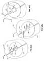
- FIG. 1is an exploded perspective view showing an internal mirror, Cassegrain-type concentrating solar collector 100 according to an embodiment of the present invention.
- Concentrating solar collector 100generally includes an optical element 110 , a photovoltaic cell 120 , a primary mirror 130 , and a secondary mirror 140 .
- Optical element 110is a solid, disk-like, light-transparent structure including an upper layer 111 , a relatively large convex surface 112 protruding from a lower side of upper layer 111 , a substantially flat aperture surface 115 disposed on an upper side of upper layer 111 , and a relatively small concave (curved) surface (depression) 117 defined in aperture surface 115 (i.e., extending into upper layer 111 ).
- upper layer 111may be vanishingly small.
- the concavity of secondary mirror 140may extend beyond the thickness of upper layer 111 .
- Photovoltaic cell 120is located in a central region 113 , which is located in the center of and surrounded by convex surface 112 .
- Primary mirror 130is disposed on convex surface 112 and secondary mirror 140 is disposed on concave surface 117 .
- Primary mirror 130 and secondary mirror 140are shaped and arranged such that, as described in further detail below, a light beam (ray) traveling in a predetermined direction (e.g., perpendicular to aperture surface 115 ) that enters optical element 110 through a specific region of aperture surface 115 is reflected by a corresponding region of primary mirror 130 to an associated region of secondary mirror 140 , and from the associated region of secondary mirror 140 to photovoltaic cell 120 (e.g., directly from secondary mirror 140 to photovoltaic cell 120 , or by way of a reflective or refractive surface positioned between secondary mirror and photovoltaic cell 120 ).
- directional termssuch as “upper”, “lower”, “above” and “below” are intended to provide relative positions for purposes of description, and are not intended to designate an absolute frame of reference.
- primary mirror 130 and secondary mirror 140are fabricated by sputtering or otherwise depositing a reflective mirror material (e.g., silver (Ag) or aluminum (Al)) directly onto convex surface 112 and concave surface 117 , thereby minimizing manufacturing costs and providing superior optical characteristics.
- a reflective mirror materiale.g., silver (Ag) or aluminum (Al)
- primary mirror 130substantially takes the shape of convex surface 112
- secondary mirror 140substantially takes the shape of concave surface 117 .
- optical element 110is molded or otherwise fabricated such that convex surface 112 and concave surface 117 are arranged and shaped to produce the desired mirror shapes.
- convex surface 112 and concave surface 117are arranged and shaped to produce the desired mirror shapes.
- primary mirror 130 and secondary mirror 140are effectively self-forming and self-aligning, thus eliminating expensive assembly and alignment costs associated with conventional concentrating solar collectors.
- primary mirror 130 and secondary mirror 140remain affixed to optical element 110 , their relative position is permanently set, thereby eliminating the need for adjustment or realignment that may be needed in conventional multiple-part arrangements.
- primary mirror 130 and secondary mirror 140are formed simultaneously using the same (identical) material or materials (e.g., plated Ag), thereby minimizing fabrication costs. Further, by utilizing the surfaces of optical element 110 to fabricate the mirrors, once light enters into optical element 110 through aperture surface 115 , the light is only reflected by primary mirror 130 /convex surface 112 and secondary mirror 140 /concave surface 117 before reaching photovoltaic cell 120 . As such, the light is subjected to only one air/glass interface (i.e., aperture surface 115 ), thereby minimizing losses that are otherwise experienced by conventional multi-part concentrating solar collectors. The single air/glass interface loss can be further lowered using an antireflection coating on aperture surface 115 .
- optical element 110is molded using a low-iron glass (e.g., Optiwhite glass produced by Pilkington PLC, UK) structure according to known glass molding methods. Molded low-iron glass provides several advantages over other production methods and materials, such as superior transmittance and surface characteristics (molded glass can achieve near perfect shapes due to its high viscosity, which prevents the glass from filling imperfections in the mold surface). Although molded glass is currently preferred for fabricating optical element 110 due to its superior optical characteristics, some of the advantages described herein may be achieved by optical elements formed using other light-transmitting materials and/or fabrication techniques. For example, clear plastic may be machined and polished to form single-piece optical element 110 , or separate pieces by be glued or otherwise secured to form optical element 110 .
- clear plasticmay be machined and polished to form single-piece optical element 110 , or separate pieces by be glued or otherwise secured to form optical element 110 .
- FIG. 2is a side view showing concentrating solar collector 100 during operation. Similar to conventional concentrating solar collectors, a collector positioning system (not shown; for example, the tracking system used in the MegaModuleTM system produced by Amonix, Incorporated of Torrance, Calif., USA) is utilized to position concentrating solar collector 100 such that light beams LB (e.g., solar rays) are directed into aperture surface 115 in a desired direction (e.g., perpendicular to aperture surface 115 .
- Photovoltaic cell 120is disposed substantially in a concentrating region F, which designates the region at which light beams LB are concentrated by primary mirror 130 , secondary mirror 140 and any intervening optical structures (e.g., a dielectric flux concentrator).
- concentrating region Fcoincides with a central region 113 , which has been planarized (flattened) to facilitate the mounting of photovoltaic cell 120 and associated wiring using conventional pick-and-place and/or lithographic processing.
- central region 113is located directly below and thus defined by the “shadow” of secondary mirror 120 .
- an opening 139is defined in primary mirror 130 to facilitate the passage of light through central region 113 to photovoltaic cell 120 .
- convex surface 112 , primary mirror 130 , concave surface 117 , and secondary mirror 140are centered on and substantially symmetrical about an optical axis X that extends substantially perpendicular to aperture surface 115 (i.e., the curved portions of convex surface 112 and concave surface 117 are defined by an arc rotated around optical axis X).
- the focus depthi.e., the distance between secondary mirror 140 and photovoltaic cell 120
- the focus depthmay be adjusted depending on the selected optics.
- the opticsmay be selected to produce a shorter focal length that facilitates recessing central region 113 (and, thus, photovoltaic cell 120 ) inside optical element 110 .
- the opticsmay be selected to produce a longer focal length that facilitates forming central region 113 at the end of a mesa extending below convex surface 112 .
- optical element 110may be altered to optimize a specific function. In comparison to modules constructed from larger concentrators, modules constructed from solid concentrators having a relatively small diameter will require more assembly time, for the larger number of concentrators that would be required to generate a desired power output, but such modules would incur less absorption loss than modules constructed from larger concentrators. Further, as suggested above, the shape of primary mirror 130 and secondary mirror 140 may take a wide variety of shapes in order to achieve a desired concentration region.
- optical element 110has an outer diameter of 28 mm, an outer diameter of concave 117 of 6.8 mm, and a thickness of 7.5 mm
- convex surface 112is formed as a hyperbolic surface having a radius of 15.000 mm and a conic constant of ⁇ 1.030
- depression 117is also a hyperbolic surface having a radius of 3.438 mm and a conic constant of ⁇ 2.752.
- convex surface 112is parabolic and concave surface 117 is hyperbolic.
- conic or otherwise curved surfacesmay be utilized to achieve the internal reflection necessary to transmit light to photovoltaic cell 120 .
- Photovoltaic cell 120is mounted either directly onto or adjacent to optical element 110 , depending on the location of concentration region F and the location of central region 113 .
- central region 113includes a flat, circular area located substantially at the apex of convex surface 112 .
- central area 113may be recessed into optical element 110 (i.e., nearer to concave surface 117 ), or located on a raised structure (i.e., further from concave surface 117 ).
- photovoltaic cell 120is mounted onto central region 113 by way of a gap filling transparent adhesive 128 such as silicone (e.g., polydiphenylsiloxane or polymethylphenylsiloxane) that serves to minimize the disruptive break in the refractive indicies between the outside surface of central region 113 and photovoltaic cell 120 .
- Photovoltaic cell 120can then be connected by way of standard wire bonds 124 to external wiring.
- Suitable photovoltaic (concentrator solar) cellsare produced, for example, by Spectrolab, Inc. of Sylmar, Calif., USA.
- optical element 110is utilized as the backplane structure for supporting both photovoltaic cell 120 and conductors 121 and 122 that are connected to photovoltaic cell 120 by way of conventional wire bond structures 124 and/or soldered interconnections.
- conductors 121 and 122may be formed, for example, printing or etching conductive material over primary mirror 130 , e.g., by way of an insulation (dielectric) layer.
- the primary mirror materialis utilized to form the conductive path (i.e., thus obviating the need for separate conductors 121 and 122 ).
- FIGS. 3 and 4are top-side exploded perspective and bottom-side assembled perspective views showing a concentrating solar collector 200 according to another embodiment of the present invention.
- concentrating solar collector 200includes an optical element 210 , a photovoltaic cell 220 , a primary mirror 230 , and a secondary mirror 240 .
- Optical element 210is similar in shape to optical element 110 , and includes upper region 211 , a relatively large convex surface 212 , a substantially flat aperture surface 215 , and a relatively small concave surface 217 .
- Photovoltaic cell 120is located in a central region 213 .
- Primary mirror 230 and secondary mirror 240are formed on convex surface 212 and concave surface 217 , respectively, substantially in the manner described above, but with the feature described below.
- a peripheral edge of upper region 211 of optical element 210includes six contiguous facets 219 . As discussed in further detail below, this six-sided arrangement facilitates the formation of large arrays of concentrating solar collectors 200 in a highly space-efficient manner. In other embodiments, less space-efficient concentrating solar collector arrays may be produced using concentrators having other peripheral shapes (e.g., the circular peripheral shape of concentrator 100 , described above).
- primary mirror 230includes a first metal film portion 231 disposed on a first half of convex surface 212 , and a second metal film portion 234 disposed on a second half of convex surface 212 .
- First metal film portion 231includes a half-hexagonal peripheral edge 232 and a substantially semi-circular inner edge 233
- second metal film portion 234includes a half-hexagonal peripheral edge 235 and a substantially semi-circular inner edge 236 .
- a thin gap 237which is made as narrow as possible to avoid the loss of reflected light, is defined between inner edges 233 and 236 to facilitate electrical isolation between metal film portions 231 and 234 .
- primary mirror 230includes a corresponding flattened structure including a first flattened portion 238 A that is integrally connected to first metal film portion 231 , and a second flattened portion 238 B that is integrally connected to second metal film portion 234 .
- these flattened portionsare also separated by gap 237 , and one of these flattened portions (e.g., first flattened portion 238 A) defines an opening 239 that coincides with optical axis X to facilitate the passage of reflected light to photovoltaic cell 220 , which is secured to flattened central region 213 substantially as described above and shown in FIG. 4 .
- one of these flattened portionse.g., first flattened portion 238 A
- FIG. 5is a perspective view showing a solid, light-transparent optical panel 300 according to another embodiment of the present invention
- FIG. 6is a simplified side view showing a concentrating solar collector array 400 A including optical panel 300 .
- optical panel 300is a solid, light-transparent plate that includes a integrated array of optical element portions 210 - 1 to 210 - 7 (delineated by dashed lines) arranged in a honeycomb pattern, where each optical element portion 210 - 1 to 210 - 7 is substantially identical to optical element 210 (which is described above with reference to FIGS. 3 and 4 ).
- optical panel 300includes a lower surface 305 having multiple protuberances (convex surfaces) 212 that are separated by troughs 307 (indicated in FIG.
- aperture surface 315including relatively small, spaced-apart depressions (convex surfaces) 217 , with each protuberance 212 and associated depression 217 being symmetrical about an associated optical axis X- 1 to X- 7 that passes through a center of both structures.
- optical element portion 210 - 1includes a protuberance 212 - 1 and a depression 217 - 1 that are symmetrical and about and intersected by an optical axis X- 1 .
- aperture surface 315is collectively formed by adjoining aperture surface portions 215 of the adjacent optical element portions.
- a section 315 - 1 of aperture surface 315is formed by aperture surface portion 215 - 1 of optical element portion 210 - 1 and aperture surface portion 215 - 2 of optical element portion 210 - 2 .
- An advantage provided by optical panel 300is that it facilitates arraying many small concentrators together in a space efficient manner in order to keep the volume of glass from becoming excessively large, and to keep the amount of power per PV cell manageable without active cooling. Further, aperture surface 315 is essentially flat, and therefore relatively easy to clean, thus minimizing maintenance costs.
- optical element panel 300is 5 to 20 mm thick, and each concentrator 200 is 20 to 80 mm wide. Therefore, optical panel 300 is relatively thin and flat, and therefore relatively easy to mold.
- FIG. 6shows a section of array 400 A including concentrating solar collectors 200 - 1 , 200 - 2 and 200 - 3 electrically connected in series, where each concentrating solar collectors 200 - 1 , 200 - 2 and 200 - 3 is substantially identical to concentrating solar collector 200 (described above with reference to FIG. 4 ).
- the metal film portions of adjacent collectorsare integrally connected at adjacent troughs, and the metal film portions of adjacent collectors of adjacent collector is electrically coupled by an associated photovoltaic cell, thereby forming a conductive path between adjacent collectors.
- metal film portions 231 - 1 and 234 - 1 of collector 200 - 1are electrically coupled by photovoltaic cell 220 - 1 , and metal film portion 234 - 1 of collector 200 - 1 is connected to metal film portion 234 - 2 of collector 200 - 2 at trough 307 - 1 .
- Collectors 200 - 2 and 200 - 3are similarly linked together, thereby forming a series-connected “row” of collectors including collectors 200 - 1 , 200 - 2 and 200 - 3 .
- each collector 200 - 1 , 200 - 2 and 200 - 3also includes a bypass diode 225 , each bypass diode having an anode connected to its first metal film portion 231 and a cathode connected to its second metal film portion 234 .
- collector 200 - 1includes a diode 225 - 1 having an anode connected to metal film portion 231 - 1 and a cathode connected to metal film portion 234 - 1 .
- Bypass diodes 225facilitate series operation (i.e., avoid an open circuit condition) by facilitating bypass of a malfunctioning collector due to failure of its photovoltaic cell.
- bypass resistorsrepresent only one circuit for facilitating such series operation.
- FIG. 7is a cross-sectional side view showing concentrating solar collector 200 - 8 according to another embodiment of the present invention.
- Concentrating solar collector 200 - 8is essentially identical to collectors 200 - 1 to 200 - 7 (discussed above) with the following optional features.
- concentrating solar collector 200 - 8utilizes surface mount integrated circuit packages to mount photovoltaic cell 220 and bypass diode 225 onto metal film portions 231 and 234 .
- bypass diode 225is mounted, for example, using solder bumps, such that bypass diode 225 straddles gap 237 , with its anode being connected to an extended portion of metal film portion 231 , and its cathode terminal being connected to an extended portion of metal film portion 234 .
- photodiode cell 220includes a front-side mounting package that facilitates mounting onto metal film portion 231 such that a light-receiving region of photodiode cell 220 is located over opening 239 .
- concentrating solar collector 200 - 8includes a heat sink that is mounted to a backside surface of photodiode cell 220 , and includes arms that connect to metal film portions 231 and 234 , thus facilitating efficient heat transfer during operation.
- heat sink 230may also provide at least part of the electrical connection of photodiode cell 220 to at least one of metal film portions 231 and 234 (e.g., by connecting an anode of photodiode cell 220 to metal film portion 234 .
- photodiode cells and bypass diodesmay be mounted onto special heat sink structures that provide all electrical connections to the primary mirror metal film sections when mounted onto an associated protrusion, thereby facilitating a convenient vehicle for testing the photodiode cells before mounting into an array.
- the photovoltaic cellsmay be recessed into the optical panel, and the heat sink implemented as a substrate that brides across or otherwise connected to the mirror metal film sections located on the edges of the recessed region.
- a sealant structure 720(e.g., glass or plastic) is formed over secondary mirror 240 such that secondary mirror 240 is sealed between a contoured (curved) lower surface 722 of sealant structure 720 and concave surface 217 of optical panel portion 210 - 8 .
- An upper surface 725 of sealant structure 720is flat and coplanar with upper surface 215 / 315 of portion 210 - 8 /optical panel 300 .
- Sealant structure 720serves to further simplify the maintenance/cleaning process by providing a completely flat surface, and also serves to protect secondary mirror 240 from corrosion due to environmental exposure.
- a similar sealant layer and/or reinforcing structuremay be provided on the lower side of the optical panel for added strength and to protect the primary mirror films.
- FIGS. 8(A) , 8 (B) and 8 (C)are perspective views illustrating lower central regions of an exemplary concentrating solar collector 200 - 9 during a production process according to another embodiment of the present invention.
- Concentrating solar collector 200 - 9is essentially identical to collectors 200 - 1 to 200 - 7 (discussed above) with the following additional features.
- metal films 231 and 234are formed as described above with flat portions 238 A and 238 B, respectively.
- flat portion 238 A of metal film 231is provided with a protruding section 804 that defines opening 239
- flat portion 238 B of metal film 234defines a recessed region 808 that provides the necessary area for protruding section 804 while separation gap 237 between inside edges 233 and 236 .
- a dielectric layer 810e.g., a solder mask
- bridging gap 237and vias 820 and 825 are defined through dielectric layer 810 to expose underlying surfaces of flat portions 238 A and 238 B.
- the dielectric layercan be applied by known techniques such as jet printing or screen printing. Referring to FIG. 8(C) , high-speed pick-and-place equipment is then used to place photovoltaic cell 220 and bypass diode 225 such that solder bumps extending from lower surfaces of the associated packages (or bare dies) are respectively positioned over associated vias formed in dielectric layer 810 . A solder reflow process is then performed to secure photovoltaic cell 220 and bypass diode 225 to flat metal film portions 238 A and 238 B.
- solder bump connection of photovoltaic cell 220 to the peripheral edges of protruding section 804(FIG. 8 (B)), thus requiring a separate connection to metal film 234 .
- this connectionis effected by an optional wire bonding process to generate a wire bond 815 between, for example, an anode or cathode of photovoltaic cell 220 and flat portion 238 B of metal film 234 .
- FIG. 9is a bottom-side perspective view showing a concentrating solar collector array 400 B produced in accordance with another embodiment of the present invention.
- Array 400 Bincludes several collectors 200 - 11 to 200 - 14 , 200 - 21 to 200 - 25 , and 200 - 31 to 200 - 34 that are arranged in parallel rows, with collectors 200 - 11 to 200 - 14 forming a first row, collectors 200 - 21 to 200 - 25 forming a second row, and 200 - 31 to 200 - 34 forming a third row.
- Each collector shown in FIG. 9is substantially the same as collector 200 - 9 shown in FIG. 8 .
- the metal film segments of each collectorare electrically coupled by an associated photodiode cell and optional bypass diode.
- metal films 231 - 11 and 234 - 11which are separated by gap 237 - 11 , are electrically coupled by photodiode cell 220 - 11 and bypass diode 225 - 11 in the manner described above.
- the metal films of each adjacent collector in each roware connected to form an associated metal film segment.
- metal film 234 - 11 of collector 200 - 11 and metal film 231 - 12 of collector 200 - 12are connected along seam 901 to form a substantially half hour-glass-shaped metal film segment 900 - 11 .
- metal film 234 - 12 of collector 200 - 12 and metal film 231 - 13 of collector 200 - 13are connected along an associated seam 901 to form metal film segment 900 - 12 .
- a conductive path for the row including collectors 200 - 11 to 200 - 14is formed by metal film segments 900 - 11 to 900 - 14 .
- a conductive path for the row including collectors 200 - 21 to 200 - 25is formed by metal film segments 900 - 21 to 900 - 25
- a conductive path for the row including collectors 200 - 31 to 200 - 34is formed by metal film segments 900 - 31 to 900 - 34 .
- metal film segments 900 - 11 to 900 - 14are separated from metal film segments 900 - 21 to 900 - 25 by an elongated gap 937 - 12 .
- metal film segments 900 - 21 to 900 - 25are separated from metal film segments 900 - 31 to 900 - 34 by an elongated gap 937 - 34 .
- metal film segments 900 - 11 to 900 - 34consist of a layer of sputtered silver on the optical panel.
- a maskis then formed, for example, using known wax-printing techniques. Two-sided printing can be employed in order to define the two sides of the optic.
- the optical panelis then immersed one or more plating baths to build up the metal thickness required for the string wiring.
- layers of electroplated copper and nickelformed on the silver but do not plate onto the mask.
- the copperwould need to be on the order of 1 micron thick in order to serve as a sufficiently conductive layer to limit the electrical loss to less than 1% of the converted power.
- the maskis stripped and the metal mirror coating is etched away, using the plated metal as an etch mask.
- the intentis to etch the mirror metal away from the clear aperture (exposing an anti-reflective coating formed thereon) on the upper side, and opening up the gaps 237 and 937 on the lower side to form the necessary metal film segments. Subsequent process, e.g., to mount photovoltaic cells, is then performed using the methods described above.
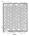
- FIG. 10is a plan view showing a concentrating solar collector unit 400 C according to another embodiment of the present invention.
- Concentrating solar collector unit 400 Cincludes an optical panel 300 C formed in the manner described above, a metal support frame 410 (e.g., aluminum or steel) for supporting and protecting optical panel 300 C, and a socket connector 420 for mounting collector unit 400 C in a collector array network (not shown).
- Optical panel 300 Cinclude several rows of concentrating solar collectors that are linked as described above by metal film segments 900 - 11 to 900 - 87 .
- End segments 910 - 12 , 910 - 23 , 910 - 34 , 910 - 45 , 910 - 56 , 910 - 67 , and 910 - 78provide connections between adjacent rows in the indicated manner, and partial segments 910 - 1 and 910 - 8 are utilized in conjunction with metallization segment 910 - 81 to provide connections between the collectors and socket connector 420 .
- the depicted segment patternis greatly simplified and provided only for illustrative purposes, and those skilled in the art will recognize that many alternative patterns may be used.
- each adjacentincludes, for example, the dielectric regions and circuit components described above (e.g., photovoltaic cell 200 - 11 is indicated between segments 900 - 11 and 900 - 12 ).
- photovoltaic cell 200 - 11is indicated between segments 900 - 11 and 900 - 12 .
- all of the collectors depicted in unit 400 Care connected in one serial string that includes all eight rows linked by end segments, it is understood that a two or more serial strings may be formed in a similar manner on each unit.
- the present inventionhas been described with respect to certain specific embodiments, it will be clear to those skilled in the art that the inventive features of the present invention are applicable to other embodiments as well, all of which are intended to fall within the scope of the present invention.
- some beneficial aspects of the inventionmay be achieved in a two-pane arrangement where the secondary mirrors are formed on a first (front) pane and the primary mirrors are formed on a second (back) pane in the manner described above.
- the primary and secondary mirrorsmay be preformed and then mounted to the optical element using a suitable adhesive, but this approach may substantially increase production costs.
- the curved surface utilized to form the secondary mirrormay be convex instead of concave, thus being in the form of a classical Gregorian type system.
- the curved surfaces utilized to form the primary and secondary mirrorsmay be elliptical, ellipsoidal, spherical, or other curved shape.
Landscapes
- Engineering & Computer Science (AREA)
- Physics & Mathematics (AREA)
- Life Sciences & Earth Sciences (AREA)
- Sustainable Development (AREA)
- Sustainable Energy (AREA)
- Thermal Sciences (AREA)
- Chemical & Material Sciences (AREA)
- Combustion & Propulsion (AREA)
- Mechanical Engineering (AREA)
- General Engineering & Computer Science (AREA)
- Photovoltaic Devices (AREA)
- Optical Elements Other Than Lenses (AREA)
Abstract
Description
Claims (25)
Priority Applications (9)
| Application Number | Priority Date | Filing Date | Title |
|---|---|---|---|
| US11/110,611US7906722B2 (en) | 2005-04-19 | 2005-04-19 | Concentrating solar collector with solid optical element |
| AU2006201575AAU2006201575B2 (en) | 2005-04-19 | 2006-04-13 | Concentrating solar collector with solid optical element |
| JP2006111486AJP5016251B2 (en) | 2005-04-19 | 2006-04-14 | Concentrating optical energy collector using solid optical components |
| CN201410212425.9ACN104052389B (en) | 2005-04-19 | 2006-04-18 | There is the concentrating solar collector of solid optical element |
| CNA2006100770223ACN1854637A (en) | 2005-04-19 | 2006-04-18 | Concentrating solar collector with solid optical element |
| BRPI0601296-5ABRPI0601296A (en) | 2005-04-19 | 2006-04-19 | concentration solar collector with solid optical element |
| PT61127486TPT1715260E (en) | 2005-04-19 | 2006-04-19 | SOLAR CONCENTRATOR COLLECTOR WITH SOLID OPTICAL ELEMENT |
| EP06112748.6AEP1715260B1 (en) | 2005-04-19 | 2006-04-19 | Concentrating solar collector with solid optical element |
| IL175007AIL175007A (en) | 2005-04-19 | 2006-04-20 | Concentrating solar collector with solid optical element |
Applications Claiming Priority (1)
| Application Number | Priority Date | Filing Date | Title |
|---|---|---|---|
| US11/110,611US7906722B2 (en) | 2005-04-19 | 2005-04-19 | Concentrating solar collector with solid optical element |
Publications (2)
| Publication Number | Publication Date |
|---|---|
| US20060231133A1 US20060231133A1 (en) | 2006-10-19 |
| US7906722B2true US7906722B2 (en) | 2011-03-15 |
Family
ID=36678538
Family Applications (1)
| Application Number | Title | Priority Date | Filing Date |
|---|---|---|---|
| US11/110,611Active2027-12-13US7906722B2 (en) | 2005-04-19 | 2005-04-19 | Concentrating solar collector with solid optical element |
Country Status (8)
| Country | Link |
|---|---|
| US (1) | US7906722B2 (en) |
| EP (1) | EP1715260B1 (en) |
| JP (1) | JP5016251B2 (en) |
| CN (2) | CN1854637A (en) |
| AU (1) | AU2006201575B2 (en) |
| BR (1) | BRPI0601296A (en) |
| IL (1) | IL175007A (en) |
| PT (1) | PT1715260E (en) |
Cited By (31)
| Publication number | Priority date | Publication date | Assignee | Title |
|---|---|---|---|---|
| US20090071467A1 (en)* | 2005-07-28 | 2009-03-19 | Light Prescriptions Innovators, Llc | Multi-junction solar cells with a homogenizer system and coupled non-imaging light concentrator |
| US20100313955A1 (en)* | 2009-06-11 | 2010-12-16 | Energy Focus, Inc. | Method of Making Solar Collector Assemblies with Optical Concentrator Encapsulant |
| US20130342742A1 (en)* | 2012-06-21 | 2013-12-26 | Broadcom Corporation | Imaging enhancements for mobile devices using optical path folding |
| US8702259B2 (en) | 2011-09-16 | 2014-04-22 | Lighting Science Group Corporation | Color conversion occlusion and associated methods |
| US8761593B2 (en) | 2010-11-10 | 2014-06-24 | Uri Neta | Common focus energy emitter |
| US8864340B2 (en) | 2009-10-05 | 2014-10-21 | Lighting Science Group Corporation | Low profile light having concave reflector and associated methods |
| US20140345672A1 (en)* | 2011-07-11 | 2014-11-27 | Matteo Repetto | Photovoltaic device |
| US8941329B2 (en) | 2011-12-05 | 2015-01-27 | Biological Illumination, Llc | Tunable LED lamp for producing biologically-adjusted light |
| US8963450B2 (en) | 2011-12-05 | 2015-02-24 | Biological Illumination, Llc | Adaptable biologically-adjusted indirect lighting device and associated methods |
| US9024536B2 (en) | 2011-12-05 | 2015-05-05 | Biological Illumination, Llc | Tunable LED lamp for producing biologically-adjusted light and associated methods |
| US9028091B2 (en) | 2009-10-05 | 2015-05-12 | Lighting Science Group Corporation | Low profile light having elongated reflector and associated methods |
| US9131573B2 (en) | 2011-12-05 | 2015-09-08 | Biological Illumination, Llc | Tunable LED lamp for producing biologically-adjusted light |
| US9127818B2 (en) | 2012-10-03 | 2015-09-08 | Lighting Science Group Corporation | Elongated LED luminaire and associated methods |
| US9151482B2 (en) | 2011-05-13 | 2015-10-06 | Lighting Science Group Corporation | Sealed electrical device with cooling system |
| US9157581B2 (en) | 2009-10-05 | 2015-10-13 | Lighting Science Group Corporation | Low profile luminaire with light guide and associated systems and methods |
| US9220202B2 (en) | 2011-12-05 | 2015-12-29 | Biological Illumination, Llc | Lighting system to control the circadian rhythm of agricultural products and associated methods |
| US9289574B2 (en) | 2011-12-05 | 2016-03-22 | Biological Illumination, Llc | Three-channel tuned LED lamp for producing biologically-adjusted light |
| US9318636B2 (en) | 2012-12-11 | 2016-04-19 | International Business Machines Corporation | Secondary optic for concentrating photovoltaic device |
| US9322516B2 (en) | 2012-11-07 | 2016-04-26 | Lighting Science Group Corporation | Luminaire having vented optical chamber and associated methods |
| US9347655B2 (en) | 2013-03-11 | 2016-05-24 | Lighting Science Group Corporation | Rotatable lighting device |
| US9360202B2 (en) | 2011-05-13 | 2016-06-07 | Lighting Science Group Corporation | System for actively cooling an LED filament and associated methods |
| US9429294B2 (en) | 2013-11-11 | 2016-08-30 | Lighting Science Group Corporation | System for directional control of light and associated methods |
| US9459397B2 (en) | 2013-03-12 | 2016-10-04 | Lighting Science Group Corporation | Edge lit lighting device |
| US9532423B2 (en) | 2010-07-23 | 2016-12-27 | Lighting Science Group Corporation | System and methods for operating a lighting device |
| US9581756B2 (en) | 2009-10-05 | 2017-02-28 | Lighting Science Group Corporation | Light guide for low profile luminaire |
| US9595118B2 (en) | 2011-05-15 | 2017-03-14 | Lighting Science Group Corporation | System for generating non-homogenous light and associated methods |
| US9693414B2 (en) | 2011-12-05 | 2017-06-27 | Biological Illumination, Llc | LED lamp for producing biologically-adjusted light |
| US9827439B2 (en) | 2010-07-23 | 2017-11-28 | Biological Illumination, Llc | System for dynamically adjusting circadian rhythm responsive to scheduled events and associated methods |
| US10490682B2 (en) | 2018-03-14 | 2019-11-26 | National Mechanical Group Corp. | Frame-less encapsulated photo-voltaic solar panel supporting solar cell modules encapsulated within multiple layers of optically-transparent epoxy-resin materials |
| US10931858B2 (en)* | 2019-04-25 | 2021-02-23 | The Boeing Company | Multi-plane image sensors for high resolution destination detection and tracking |
| US11552592B2 (en) | 2017-12-07 | 2023-01-10 | Commissariat A L'energie Atomique Et Aux Energies Alternatives | Manufacturing a concentrating sub-module comprising a heat-dissipating material |
Families Citing this family (120)
| Publication number | Priority date | Publication date | Assignee | Title |
|---|---|---|---|---|
| US7906722B2 (en) | 2005-04-19 | 2011-03-15 | Palo Alto Research Center Incorporated | Concentrating solar collector with solid optical element |
| US8063300B2 (en)* | 2005-05-26 | 2011-11-22 | Solfocus, Inc. | Concentrator solar photovoltaic array with compact tailored imaging power units |
| US20090056790A1 (en)* | 2005-05-26 | 2009-03-05 | Solfocus, Inc. | Monolithic Mirror Array |
| WO2007103994A2 (en)* | 2006-03-08 | 2007-09-13 | Light Prescriptions Innovators, Llc | Multi-junction solar cells with a homogenizer system and coupled non-imaging light concentrator |
| EP1920285A4 (en) | 2005-07-28 | 2010-11-03 | Light Prescriptions Innovators | OPEN-FREE LENTICULAR OPTICAL ELEMENTS AND THEIR APPLICATION TO CAPACITORS AND PROJECTORS |
| US20080047605A1 (en)* | 2005-07-28 | 2008-02-28 | Regents Of The University Of California | Multi-junction solar cells with a homogenizer system and coupled non-imaging light concentrator |
| US7765949B2 (en) | 2005-11-17 | 2010-08-03 | Palo Alto Research Center Incorporated | Extrusion/dispensing systems and methods |
| US7799371B2 (en) | 2005-11-17 | 2010-09-21 | Palo Alto Research Center Incorporated | Extruding/dispensing multiple materials to form high-aspect ratio extruded structures |
| US20070107773A1 (en) | 2005-11-17 | 2007-05-17 | Palo Alto Research Center Incorporated | Bifacial cell with extruded gridline metallization |
| US8283554B2 (en)* | 2005-12-19 | 2012-10-09 | Corning Incorporated | Method and apparatus for concentrating light |
| US7877921B1 (en) | 2006-03-06 | 2011-02-01 | Raytheon Company | Method and apparatus for combining light from two sources to illuminate a reticle |
| US7855335B2 (en) | 2006-04-26 | 2010-12-21 | Palo Alto Research Center Incorporated | Beam integration for concentrating solar collector |
| US7638708B2 (en) | 2006-05-05 | 2009-12-29 | Palo Alto Research Center Incorporated | Laminated solar concentrating photovoltaic device |
| US7851693B2 (en)* | 2006-05-05 | 2010-12-14 | Palo Alto Research Center Incorporated | Passively cooled solar concentrating photovoltaic device |
| US8713845B1 (en)* | 2006-08-01 | 2014-05-06 | Raytheon Canada Limited | Method and apparatus for efficiently collecting radiation |
| US7922471B2 (en) | 2006-11-01 | 2011-04-12 | Palo Alto Research Center Incorporated | Extruded structure with equilibrium shape |
| US8226391B2 (en) | 2006-11-01 | 2012-07-24 | Solarworld Innovations Gmbh | Micro-extrusion printhead nozzle with tapered cross-section |
| US8322025B2 (en) | 2006-11-01 | 2012-12-04 | Solarworld Innovations Gmbh | Apparatus for forming a plurality of high-aspect ratio gridline structures |
| US7780812B2 (en) | 2006-11-01 | 2010-08-24 | Palo Alto Research Center Incorporated | Extrusion head with planarized edge surface |
| US7928015B2 (en) | 2006-12-12 | 2011-04-19 | Palo Alto Research Center Incorporated | Solar cell fabrication using extruded dopant-bearing materials |
| US7638438B2 (en) | 2006-12-12 | 2009-12-29 | Palo Alto Research Center Incorporated | Solar cell fabrication using extrusion mask |
| US20080142000A1 (en)* | 2006-12-15 | 2008-06-19 | Sol Focus, Inc. | Optic spacing nubs |
| US20080185032A1 (en)* | 2007-02-02 | 2008-08-07 | Macdonald Robert | Discrete secondary reflector for solid concentrator |
| WO2008097688A1 (en) | 2007-02-02 | 2008-08-14 | Solfocus, Inc. | Thermal spray for solar concentrator fabrication |
| US20080203411A1 (en)* | 2007-02-27 | 2008-08-28 | Hing Wah Chan | Direct attachment of optically-active device to optical element |
| US20090025784A1 (en)* | 2007-02-02 | 2009-01-29 | Sol Focus, Inc. | Thermal spray for solar concentrator fabrication |
| WO2008097805A2 (en)* | 2007-02-02 | 2008-08-14 | Solfocus, Inc. | Conductor fabrication for optical element |
| AU2008218103B2 (en)* | 2007-02-23 | 2012-12-06 | The Regents Of The University Of California | Concentrating photovoltaic system using a fresnel lens and nonimaging secondary optics |
| US20090231739A1 (en)* | 2007-05-07 | 2009-09-17 | The Regents Of The University Of California A California Corporation | Matrix formulation of kohler integrating system and coupled non-imaging light concentrator |
| US7954449B2 (en) | 2007-05-08 | 2011-06-07 | Palo Alto Research Center Incorporated | Wiring-free, plumbing-free, cooled, vacuum chuck |
| US20080282828A1 (en)* | 2007-05-19 | 2008-11-20 | The Boeing Company | Pointing a plurality of elements in the same direction |
| US7671270B2 (en)* | 2007-07-30 | 2010-03-02 | Emcore Solar Power, Inc. | Solar cell receiver having an insulated bypass diode |
| US20090056789A1 (en)* | 2007-08-30 | 2009-03-05 | Vladimir Draganov | Solar concentrator and solar concentrator array |
| US20090107540A1 (en)* | 2007-10-30 | 2009-04-30 | Solfocus, Inc. | Non-Imaging Concentrator With Spacing Nubs |
| US20090114265A1 (en)* | 2007-11-03 | 2009-05-07 | Solfocus, Inc. | Solar Concentrator |
| US20090120500A1 (en)* | 2007-11-14 | 2009-05-14 | Eric Prather | Solar cell package for solar concentrator |
| DE112009001122A5 (en) | 2008-05-07 | 2011-03-24 | Peter Dr.-Ing. Draheim | Apparatus and method for concentrating incident light |
| CN102113135B (en) | 2008-05-12 | 2014-10-22 | 亚利桑那大学董事会 | Photovoltaic generator with a spherical imaging lens for use with a paraboloidal solar reflector |
| PT104064A (en)* | 2008-05-19 | 2009-11-19 | Manuel Pedro Ivens Col Pereira | ADJUSTED PRIMARY CONCENTRATORS COMBINED WITH SECONDARY ASSOCIATED WITH MULTIPLE RECEPTORS AND WITH CONVECTION REDUCTION |
| US7928316B2 (en) | 2008-06-05 | 2011-04-19 | Solfocus, Inc. | Solar concentrator backpan |
| US7999175B2 (en) | 2008-09-09 | 2011-08-16 | Palo Alto Research Center Incorporated | Interdigitated back contact silicon solar cells with laser ablated grooves |
| US20100071768A1 (en)* | 2008-09-25 | 2010-03-25 | Solapoint Corporation | Enhanced solar collector |
| US8730179B2 (en)* | 2008-09-30 | 2014-05-20 | Apple Inc. | Integrated touch sensor and solar assembly |
| US9127822B2 (en)* | 2008-10-10 | 2015-09-08 | Sunflower Corporation | Afocal optical concentrator |
| US20100108121A1 (en)* | 2008-10-30 | 2010-05-06 | Solapoint Corporation | Concentrating solar cell module |
| US8117983B2 (en)* | 2008-11-07 | 2012-02-21 | Solarworld Innovations Gmbh | Directional extruded bead control |
| US20100122721A1 (en)* | 2008-11-18 | 2010-05-20 | Solapoint Corporation | Array type concentrating solar cell system |
| US8080729B2 (en) | 2008-11-24 | 2011-12-20 | Palo Alto Research Center Incorporated | Melt planarization of solar cell bus bars |
| US8960120B2 (en) | 2008-12-09 | 2015-02-24 | Palo Alto Research Center Incorporated | Micro-extrusion printhead with nozzle valves |
| WO2010091391A2 (en)* | 2009-02-09 | 2010-08-12 | Semprius, Inc. | Concentrator-type photovoltaic (cpv) modules, receivers and sub-receivers and methods of forming same |
| JP5493075B2 (en)* | 2009-02-24 | 2014-05-14 | 株式会社クリーンベンチャー21 | Concentrating solar cell and tracking solar cell device using the same |
| US20100218807A1 (en)* | 2009-02-27 | 2010-09-02 | Skywatch Energy, Inc. | 1-dimensional concentrated photovoltaic systems |
| TWI395914B (en)* | 2009-04-09 | 2013-05-11 | Univ Nat Cheng Kung | Multiple solar concentrator system |
| WO2010131164A2 (en)* | 2009-05-14 | 2010-11-18 | Aerosun Technologies Ag | Solar concentrator |
| EP2436041A2 (en)* | 2009-05-26 | 2012-04-04 | Cogenra Solar, Inc. | Concentrating solar photovoltaic-thermal system |
| US8684545B2 (en) | 2009-07-30 | 2014-04-01 | The Regents Of The University Of California | Light concentration apparatus, systems and methods |
| US9039213B2 (en) | 2009-07-30 | 2015-05-26 | The Regents Of The University Of California | Light concentration apparatus, systems and methods |
| US8648245B1 (en) | 2009-08-07 | 2014-02-11 | The Boeing Company | AMTEC power system with thermal block |
| US8281783B2 (en)* | 2009-08-07 | 2012-10-09 | The Boeing Company | Thermal absorber with gravity counterflow regeneration for solar AMTEC power systems |
| US8378208B1 (en) | 2009-08-07 | 2013-02-19 | The Boeing Company | AMTEC power system with thermal block |
| US8629345B1 (en) | 2009-08-26 | 2014-01-14 | The Boeing Company | Solar AMTEC power system |
| US8575468B2 (en)* | 2009-08-26 | 2013-11-05 | The Boeing Company | Solar AMTEC power system |
| US8344237B1 (en)* | 2009-10-27 | 2013-01-01 | The Boeing Company | AMTEC power system |
| WO2011058941A1 (en)* | 2009-11-10 | 2011-05-19 | 京セラ株式会社 | Photovoltaic conversion device, package for accommodating photovoltaic conversion element, and photovoltaic conversion module |
| US20110017267A1 (en)* | 2009-11-19 | 2011-01-27 | Joseph Isaac Lichy | Receiver for concentrating photovoltaic-thermal system |
| JP5557144B2 (en)* | 2010-03-03 | 2014-07-23 | 正孝 白▲崎▼ | Optical instruments |
| US8708507B2 (en) | 2010-03-03 | 2014-04-29 | Masataka Shirasaki | Optical apparatus for magnifying a view of an object at a distance |
| US20110226307A1 (en)* | 2010-03-19 | 2011-09-22 | Solapoint Corporation | Three-dimensional type concentrating solar cell system |
| WO2011127572A1 (en)* | 2010-04-13 | 2011-10-20 | John Robert Mumford | Solar concentrators, solar collectors and methods of making same |
| US20110271999A1 (en) | 2010-05-05 | 2011-11-10 | Cogenra Solar, Inc. | Receiver for concentrating photovoltaic-thermal system |
| US8686279B2 (en)* | 2010-05-17 | 2014-04-01 | Cogenra Solar, Inc. | Concentrating solar energy collector |
| US8669462B2 (en) | 2010-05-24 | 2014-03-11 | Cogenra Solar, Inc. | Concentrating solar energy collector |
| CN102315292A (en)* | 2010-06-30 | 2012-01-11 | 富准精密工业(深圳)有限公司 | Solar battery device |
| CN102386966B (en)* | 2010-08-31 | 2014-12-03 | 成都易生玄科技有限公司 | Systematized integration for collecting energy source-level light |
| US9893223B2 (en) | 2010-11-16 | 2018-02-13 | Suncore Photovoltaics, Inc. | Solar electricity generation system |
| US8040609B1 (en) | 2010-11-29 | 2011-10-18 | Palo Alto Research Center Incorporated | Self-adjusting solar light transmission apparatus |
| US8884156B2 (en) | 2010-11-29 | 2014-11-11 | Palo Alto Research Center Incorporated | Solar energy harvesting device using stimuli-responsive material |
| CN102148589A (en)* | 2010-12-30 | 2011-08-10 | 中国科学院长春光学精密机械与物理研究所 | High-power solar energy concentrated photovoltaic system based on Cassegrain structure |
| US8816188B2 (en) | 2011-04-20 | 2014-08-26 | Hewlett-Packard Development Company, L.P. | Photovoltaic devices with electrically coupled supports |
| CN102291049A (en)* | 2011-08-12 | 2011-12-21 | 嘉兴市硅兴电子科技有限公司 | Intelligent energy-collecting photovoltaic panel device |
| CN102306674B (en)* | 2011-09-21 | 2012-12-26 | 福鼎市一雄光学仪器有限公司 | High-efficient solar photovoltaic battery condensation device |
| GB2495960A (en)* | 2011-10-26 | 2013-05-01 | Fromanteel Ltd | Solar concentrator |
| JP5422082B2 (en) | 2011-12-14 | 2014-02-19 | パナソニック株式会社 | Solar cell and manufacturing method thereof |
| US8752380B2 (en) | 2012-05-22 | 2014-06-17 | Palo Alto Research Center Incorporated | Collapsible solar-thermal concentrator for renewable, sustainable expeditionary power generator system |
| US20150083192A1 (en) | 2012-05-28 | 2015-03-26 | Panasonic Corporation | Solar cell and method for manufacturing same |
| JP6078869B2 (en)* | 2012-06-28 | 2017-02-15 | 株式会社Screenホールディングス | Inspection apparatus and inspection method |
| US20180347858A1 (en)* | 2012-10-18 | 2018-12-06 | Thermolift, Inc. | Combination Solar and Combustion Heater |
| US20140124014A1 (en) | 2012-11-08 | 2014-05-08 | Cogenra Solar, Inc. | High efficiency configuration for solar cell string |
| US8878050B2 (en) | 2012-11-20 | 2014-11-04 | Boris Gilman | Composite photovoltaic device with parabolic collector and different solar cells |
| US10050583B2 (en) | 2012-11-30 | 2018-08-14 | Arizona Board Of Regents On Behalf Of University Of Arizona | Solar generator with large reflector dishes and concentrator photovoltaic cells in flat arrays |
| US9270225B2 (en) | 2013-01-14 | 2016-02-23 | Sunpower Corporation | Concentrating solar energy collector |
| WO2014138857A1 (en) | 2013-03-15 | 2014-09-18 | John Paul Morgan | Light panel, optical assembly with improved interface and light panel with improved manufacturing tolerances |
| US9595627B2 (en) | 2013-03-15 | 2017-03-14 | John Paul Morgan | Photovoltaic panel |
| US9960303B2 (en) | 2013-03-15 | 2018-05-01 | Morgan Solar Inc. | Sunlight concentrating and harvesting device |
| US9714756B2 (en) | 2013-03-15 | 2017-07-25 | Morgan Solar Inc. | Illumination device |
| WO2015061323A1 (en) | 2013-10-22 | 2015-04-30 | The Arizona Board Of Regents On Behalf Of The University Of Arizona | Octohedral frame and tripod for rotating equipment |
| CN103607171B (en)* | 2013-10-30 | 2015-10-21 | 李敬宇 | Wide array flower pattern concentrating component |
| JP2015099336A (en)* | 2013-11-20 | 2015-05-28 | 株式会社東芝 | Optical element and optical device |
| CN104779312B (en)* | 2014-01-09 | 2017-10-10 | 讯芯电子科技(中山)有限公司 | Concentrating solar photovoltaic module |
| US10164140B2 (en)* | 2014-02-21 | 2018-12-25 | The Boeing Company | Modular self-tracking micro-concentrator for space power |
| US10250182B2 (en) | 2014-02-21 | 2019-04-02 | The Boeing Company | Micro-concentrator solar array using micro-electromechanical systems (MEMS) based reflectors |
| US9813022B2 (en) | 2014-02-21 | 2017-11-07 | The Boeing Company | Dynamically setting a threshold output level for a solar array |
| US10236822B2 (en) | 2014-02-21 | 2019-03-19 | The Boeing Company | Method and apparatus for calibrating a micro-concentrator solar array |
| NL2012557B1 (en)* | 2014-04-02 | 2016-02-15 | Stichting Energieonderzoek Centrum Nederland | Photovoltaic module. |
| WO2016115502A1 (en) | 2015-01-16 | 2016-07-21 | The Arizona Board Of Regents On Behalf Of The University Of Arizona | Micro-scale concentrated photovoltaic module |
| WO2016141041A1 (en) | 2015-03-02 | 2016-09-09 | The Arizona Board Of Regents On Behalf Of The University Of Arizona | Glass forming mold of adjustable shape |
| JP6384801B2 (en)* | 2015-03-11 | 2018-09-05 | パナソニックIpマネジメント株式会社 | Solar cell module |
| US10686400B2 (en) | 2015-06-12 | 2020-06-16 | THE ARIZONA BOARD OR REGENTS on behalf of THE UNIVERSITY OF ARIZONA | Tandem photovoltaic module with diffractive spectral separation |
| US10551089B2 (en) | 2015-08-03 | 2020-02-04 | The Arizona Board Of Regents On Behalf Of The University Of Arizona | Solar concentrator for a tower-mounted central receiver |
| CN105187002B (en)* | 2015-08-11 | 2017-09-08 | 上海盈达空调设备股份有限公司 | Wide spectrum electromagnetism solar cell |
| US10418501B2 (en) | 2015-10-02 | 2019-09-17 | X-Celeprint Limited | Wafer-integrated, ultra-low profile concentrated photovoltaics (CPV) for space applications |
| US10476426B2 (en) | 2015-12-09 | 2019-11-12 | Craig Bradley Edward Wildman | Systems and methods for collecting solar energy using a tilted linear solar collector |
| US20170288604A1 (en)* | 2016-04-05 | 2017-10-05 | Patrick Kenneth Powell | Solar panel design assembly |
| WO2018063348A1 (en)* | 2016-09-30 | 2018-04-05 | Chiu Chia Pin | Compound parabolic concentrator including protrusion |
| US10566926B2 (en) | 2016-10-26 | 2020-02-18 | Craig Bradley Edward Wildman | Systems and methods for collecting solar energy using a parabolic trough solar collector |
| US10432137B2 (en)* | 2017-09-25 | 2019-10-01 | Cameron Ernest Jabara | Solar energy collector and method of operation |
| FR3074964B1 (en)* | 2017-12-07 | 2019-11-29 | Commissariat A L'energie Atomique Et Aux Energies Alternatives | MANUFACTURE OF A CONCENTRATION SUB-MODULE USING PHOTOVOLTAIC ASSEMBLY METHODS |
| TWI704764B (en)* | 2019-05-10 | 2020-09-11 | 黃培勛 | Light-collecting lens, light-collecting module, solar cell device, and solar cell system |
| CN111257232A (en)* | 2020-03-19 | 2020-06-09 | 中国科学院长春光学精密机械与物理研究所 | Carbon pollution experimental device for multilayer film optical element for efficiently collecting EUV light |
| CN112968664A (en)* | 2021-02-02 | 2021-06-15 | 中国电子科技集团公司第十八研究所 | Solar cell array with intelligent spectrum matching function |
Citations (178)
| Publication number | Priority date | Publication date | Assignee | Title |
|---|---|---|---|---|
| US2031387A (en) | 1934-08-22 | 1936-02-18 | Schwarz Arthur | Nozzle |
| US2789731A (en) | 1955-06-06 | 1957-04-23 | Leonard L Marraffino | Striping dispenser |
| US3032008A (en) | 1956-05-07 | 1962-05-01 | Polaroid Corp | Apparatus for manufacturing photographic films |
| US3159313A (en) | 1961-05-16 | 1964-12-01 | Dow Chemical Co | Multi-component proportioning meter system |
| US3602193A (en) | 1969-04-10 | 1971-08-31 | John R Adams | Apparatus for preparing coatings with extrusions |
| US3973994A (en) | 1974-03-11 | 1976-08-10 | Rca Corporation | Solar cell with grooved surface |
| US3988166A (en)* | 1975-01-07 | 1976-10-26 | Beam Engineering, Inc. | Apparatus for enhancing the output of photovoltaic solar cells |
| US4018367A (en) | 1976-03-02 | 1977-04-19 | Fedco Inc. | Manifold dispensing apparatus having releasable subassembly |
| US4021267A (en) | 1975-09-08 | 1977-05-03 | United Technologies Corporation | High efficiency converter of solar energy to electricity |
| US4045246A (en) | 1975-08-11 | 1977-08-30 | Mobil Tyco Solar Energy Corporation | Solar cells with concentrators |
| US4053327A (en) | 1975-09-24 | 1977-10-11 | Communications Satellite Corporation | Light concentrating solar cell cover |
| US4084985A (en) | 1977-04-25 | 1978-04-18 | The United States Of America As Represented By The Administrator Of The National Aeronautics And Space Administration | Method for producing solar energy panels by automation |
| US4086485A (en)* | 1976-05-26 | 1978-04-25 | Massachusetts Institute Of Technology | Solar-radiation collection apparatus with tracking circuitry |
| US4095997A (en) | 1976-10-07 | 1978-06-20 | Griffiths Kenneth F | Combined solar cell and hot air collector apparatus |
| US4119058A (en) | 1976-03-11 | 1978-10-10 | Alfred Schmermund | Glue applicators |
| US4131485A (en) | 1977-08-08 | 1978-12-26 | Motorola, Inc. | Solar energy collector and concentrator |
| US4141231A (en) | 1975-07-28 | 1979-02-27 | Maschinenfabrik Peter Zimmer Aktiengesellschaft | Machine for applying patterns to a substrate |
| US4148301A (en) | 1977-09-26 | 1979-04-10 | Cluff C Brent | Water-borne rotating solar collecting and storage systems |
| US4153476A (en) | 1978-03-29 | 1979-05-08 | Nasa | Double-sided solar cell package |
| US4177083A (en) | 1977-09-06 | 1979-12-04 | Acurex Corporation | Photovoltaic concentrator |
| US4221468A (en) | 1979-02-26 | 1980-09-09 | Macken John A | Multi-cavity laser mirror |
| US4224081A (en) | 1974-11-27 | 1980-09-23 | Sharp Kabushiki Kaisha | Solar cell sealed by glass laminations |
| US4234351A (en) | 1978-07-14 | 1980-11-18 | The Boeing Company | Process for fabricating glass-encapsulated solar cell arrays and the product produced thereby |
| US4254894A (en) | 1979-08-23 | 1981-03-10 | The Continental Group, Inc. | Apparatus for dispensing a striped product and method of producing the striped product |
| US4320251A (en) | 1980-07-28 | 1982-03-16 | Solamat Inc. | Ohmic contacts for solar cells by arc plasma spraying |
| US4331703A (en) | 1979-03-28 | 1982-05-25 | Solarex Corporation | Method of forming solar cell having contacts and antireflective coating |
| US4337758A (en) | 1978-06-21 | 1982-07-06 | Meinel Aden B | Solar energy collector and converter |
| US4355196A (en) | 1981-03-11 | 1982-10-19 | The United States Of America As Represented By The Administrator Of The National Aeronautics And Space Administration | Solar cell having improved back surface reflector |
| US4461403A (en) | 1980-12-17 | 1984-07-24 | Colgate-Palmolive Company | Striping dispenser |
| US4476165A (en) | 1982-06-07 | 1984-10-09 | Acumeter Laboratories, Inc. | Method of and apparatus for multi-layer viscous fluid deposition such as for the application of adhesives and the like |
| US4490418A (en) | 1982-04-16 | 1984-12-25 | Fuji Photo Film Co., Ltd. | Coating method and apparatus |
| JPS6082680A (en) | 1983-10-07 | 1985-05-10 | Fuji Photo Film Co Ltd | Surface treating device for metallic web |
| US4521457A (en) | 1982-09-21 | 1985-06-04 | Xerox Corporation | Simultaneous formation and deposition of multiple ribbon-like streams |
| US4540843A (en) | 1983-03-09 | 1985-09-10 | Licentia Patent-Verwaltungs-Gmbh | Solar cell |
| US4602120A (en) | 1983-11-25 | 1986-07-22 | Atlantic Richfield Company | Solar cell manufacture |
| US4683348A (en) | 1985-04-26 | 1987-07-28 | The Marconi Company Limited | Solar cell arrays |
| US4711972A (en)* | 1985-07-05 | 1987-12-08 | Entech, Inc. | Photovoltaic cell cover for use with a primary optical concentrator in a solar energy collector |
| US4746370A (en) | 1987-04-29 | 1988-05-24 | Ga Technologies Inc. | Photothermophotovoltaic converter |
| US4747517A (en) | 1987-03-23 | 1988-05-31 | Minnesota Mining And Manufacturing Company | Dispenser for metering proportionate increments of polymerizable materials |
| US4792685A (en) | 1987-04-29 | 1988-12-20 | Masami Yamakawa | Photoelectric sensor |
| US4796038A (en) | 1985-07-24 | 1989-01-03 | Ateq Corporation | Laser pattern generation apparatus |
| US4826777A (en) | 1987-04-17 | 1989-05-02 | The Standard Oil Company | Making a photoresponsive array |
| US4841946A (en) | 1984-02-17 | 1989-06-27 | Marks Alvin M | Solar collector, transmitter and heater |
| US4847349A (en) | 1985-08-27 | 1989-07-11 | Mitsui Toatsu Chemicals, Inc. | Polyimide and high-temperature adhesive of polyimide from meta substituted phenoxy diamines |
| US4849028A (en) | 1986-07-03 | 1989-07-18 | Hughes Aircraft Company | Solar cell with integrated interconnect device and process for fabrication thereof |
| US4855884A (en) | 1987-12-02 | 1989-08-08 | Morpheus Lights, Inc. | Variable beamwidth stage light |
| US4938994A (en) | 1987-11-23 | 1990-07-03 | Epicor Technology, Inc. | Method and apparatus for patch coating printed circuit boards |
| US4947825A (en) | 1989-09-11 | 1990-08-14 | Rockwell International Corporation | Solar concentrator - radiator assembly |
| US4952026A (en) | 1988-10-14 | 1990-08-28 | Corning Incorporated | Integral optical element and method |
| US5000988A (en) | 1987-01-14 | 1991-03-19 | Matsushita Electric Industrial Co., Ltd. | Method of applying a coating of viscous materials |
| US5004319A (en) | 1988-12-29 | 1991-04-02 | The United States Of America As Represented By The Department Of Energy | Crystal diffraction lens with variable focal length |
| US5011565A (en) | 1989-12-06 | 1991-04-30 | Mobil Solar Energy Corporation | Dotted contact solar cell and method of making same |
| US5062899A (en) | 1990-03-30 | 1991-11-05 | The United States Of America As Represented By The Administrator Of The National Aeronautics And Space Administration | Wide acceptance angle, high concentration ratio, optical collector |
| US5075281A (en) | 1989-01-03 | 1991-12-24 | Testardi Louis R | Methods of making a high dielectric constant, resistive phase of YBA2 CU3 OX and methods of using the same |
| US5089055A (en) | 1989-12-12 | 1992-02-18 | Takashi Nakamura | Survivable solar power-generating systems for use with spacecraft |
| US5151377A (en) | 1991-03-07 | 1992-09-29 | Mobil Solar Energy Corporation | Method for forming contacts |
| US5167724A (en) | 1991-05-16 | 1992-12-01 | The United States Of America As Represented By The United States Department Of Energy | Planar photovoltaic solar concentrator module |
| US5180441A (en) | 1991-06-14 | 1993-01-19 | General Dynamics Corporation/Space Systems Division | Solar concentrator array |
| US5213628A (en) | 1990-09-20 | 1993-05-25 | Sanyo Electric Co., Ltd. | Photovoltaic device |
| US5216543A (en) | 1987-03-04 | 1993-06-01 | Minnesota Mining And Manufacturing Company | Apparatus and method for patterning a film |
| US5254388A (en) | 1990-12-21 | 1993-10-19 | Minnesota Mining And Manufacturing Company | Light control film with reduced ghost images |
| US5344496A (en)* | 1992-11-16 | 1994-09-06 | General Dynamics Corporation, Space Systems Division | Lightweight solar concentrator cell array |
| US5353813A (en) | 1992-08-19 | 1994-10-11 | Philip Morris Incorporated | Reinforced carbon heater with discrete heating zones |
| US5356488A (en) | 1991-12-27 | 1994-10-18 | Rudolf Hezel | Solar cell and method for its manufacture |
| WO1994028361A1 (en) | 1993-06-02 | 1994-12-08 | Stirbl Robert C | Method for changing solar energy distribution |
| US5389159A (en) | 1992-09-01 | 1995-02-14 | Canon Kabushiki Kaisha | Solar cell module and method for producing the same |
| US5404869A (en) | 1992-04-16 | 1995-04-11 | Tir Technologies, Inc. | Faceted totally internally reflecting lens with individually curved faces on facets |
| US5449413A (en) | 1993-05-12 | 1995-09-12 | Optical Coating Laboratory, Inc. | UV/IR reflecting solar cell cover |
| US5501743A (en) | 1994-08-11 | 1996-03-26 | Cherney; Matthew | Fiber optic power-generating system |
| US5529054A (en) | 1994-06-20 | 1996-06-25 | Shoen; Neil C. | Solar energy concentrator and collector system and associated method |
| US5536313A (en) | 1993-09-06 | 1996-07-16 | Matsushita Electric Industrial Co., Ltd. | Intermittent coating apparatus |
| US5538563A (en) | 1995-02-03 | 1996-07-23 | Finkl; Anthony W. | Solar energy concentrator apparatus for bifacial photovoltaic cells |
| US5540216A (en)* | 1994-11-21 | 1996-07-30 | Rasmusson; James K. | Apparatus and method for concentrating radiant energy emanated by a moving energy source |
| US5543333A (en) | 1993-09-30 | 1996-08-06 | Siemens Solar Gmbh | Method for manufacturing a solar cell having combined metallization |
| US5552820A (en) | 1993-05-21 | 1996-09-03 | Xerox Corporation | Fly's eye optics for a raster output scanner in an electrophotographic printer |
| US5559677A (en) | 1994-04-29 | 1996-09-24 | Motorola, Inc. | Method of forming a device by selectively thermal spraying a metallic conductive material thereon |
| US5560518A (en) | 1992-02-25 | 1996-10-01 | Cambridge Consultants Limited | Fluid delivery system |
| US5569399A (en) | 1995-01-20 | 1996-10-29 | General Electric Company | Lasing medium surface modification |
| US5590818A (en) | 1994-12-07 | 1997-01-07 | Smithkline Beecham Corporation | Mulitsegmented nozzle for dispensing viscous materials |
| US5665175A (en) | 1990-05-30 | 1997-09-09 | Safir; Yakov | Bifacial solar cell |
| US5700325A (en) | 1994-08-03 | 1997-12-23 | Matsushita Electric Industrial Co., Ltd. | Coating device and a method of coating |
| US5733608A (en) | 1995-02-02 | 1998-03-31 | Minnesota Mining And Manufacturing Company | Method and apparatus for applying thin fluid coating stripes |
| DE19735281A1 (en) | 1997-08-14 | 1999-02-18 | Rolf Hoericht | Energy generating arrangement using solar radiation |
| US5873495A (en) | 1996-11-21 | 1999-02-23 | Saint-Germain; Jean G. | Device for dispensing multi-components from a container |
| US5918771A (en) | 1996-01-31 | 1999-07-06 | Airspray International B.V. | Aerosol intended for dispensing a multi-component material |
| US5929530A (en) | 1995-08-18 | 1999-07-27 | Mcdonnell Douglas Corporation | Advanced solar controller |
| US5949123A (en) | 1995-11-13 | 1999-09-07 | Photowatt International S.A. | Solar cell including multi-crystalline silicon and a method of texturizing the surface of p-type multi-crystalline silicon |
| US5981902A (en) | 1994-12-15 | 1999-11-09 | Mitsubishi Chemical Corporation | Texturing apparatus for magnetic recording medium and magnetic recording medium process thereby |
| US5990413A (en) | 1996-06-19 | 1999-11-23 | Ortabasi; Ugur | Bifacial lightweight array for solar power |
| US6011307A (en) | 1997-08-12 | 2000-01-04 | Micron Technology, Inc. | Anisotropic conductive interconnect material for electronic devices, method of use and resulting product |
| US6020554A (en) | 1999-03-19 | 2000-02-01 | Photovoltaics International, Llc | Tracking solar energy conversion unit adapted for field assembly |
| US6047862A (en) | 1995-04-12 | 2000-04-11 | Smithkline Beecham P.L.C. | Dispenser for dispensing viscous fluids |
| US6091017A (en) | 1999-08-23 | 2000-07-18 | Composite Optics Incorporated | Solar concentrator array |
| WO2000049658A1 (en) | 1999-02-16 | 2000-08-24 | Alien Technology Corporation | Functionally symmetric integrated circuit die |
| WO2000049421A1 (en) | 1999-02-16 | 2000-08-24 | Alien Technology Corporation | Testing integrated circuit dice |
| US6118067A (en) | 1998-11-20 | 2000-09-12 | Swales Aerospace | Method and apparatus for improved solar concentration arrays |
| US6130465A (en) | 1997-10-29 | 2000-10-10 | Light Point Systems Inc. | Micro-solar assembly |
| US6140570A (en) | 1997-10-29 | 2000-10-31 | Canon Kabushiki Kaisha | Photovoltaic element having a back side transparent and electrically conductive layer with a light incident side surface region having a specific cross section and a module comprising said photovolatic element |
| US6203621B1 (en) | 1999-05-24 | 2001-03-20 | Trw Inc. | Vacuum chuck for holding thin sheet material |
| US6232217B1 (en) | 2000-06-05 | 2001-05-15 | Chartered Semiconductor Manufacturing Ltd. | Post treatment of via opening by N-containing plasma or H-containing plasma for elimination of fluorine species in the FSG near the surfaces of the via opening |
| US6257450B1 (en) | 1999-04-21 | 2001-07-10 | Pechiney Plastic Packaging, Inc. | Dual dispense container having cloverleaf orifice |
| US20010008230A1 (en) | 1996-07-08 | 2001-07-19 | David M. Keicher | Energy-beam-driven rapid fabrication system |
| US6274508B1 (en) | 1999-02-05 | 2001-08-14 | Alien Technology Corporation | Apparatuses and methods used in forming assemblies |
| US6278054B1 (en)* | 1998-05-28 | 2001-08-21 | Tecstar Power Systems, Inc. | Solar cell having an integral monolithically grown bypass diode |
| US6293498B1 (en) | 1996-06-28 | 2001-09-25 | Honeywell International Inc. | Hybrid deicing system and method of operation |
| US6310281B1 (en) | 2000-03-16 | 2001-10-30 | Global Solar Energy, Inc. | Thin-film, flexible photovoltaic module |
| US6323415B1 (en) | 1998-09-18 | 2001-11-27 | Hitachi, Ltd. | Light concentrator photovoltaic module method of manufacturing same and light concentrator photovoltaic system |
| USRE37512E1 (en) | 1995-02-21 | 2002-01-15 | Interuniversitair Microelektronica Centrum (Imec) Vzw | Method of preparing solar cell front contacts |
| JP2002111035A (en) | 2000-09-27 | 2002-04-12 | Sanyo Electric Co Ltd | Double-sided solar cell module |
| US6379521B1 (en) | 1998-01-06 | 2002-04-30 | Canon Kabushiki Kaisha | Method of producing zinc oxide film, method of producing photovoltaic element, and method of producing semiconductor element substrate |
| US20020056473A1 (en) | 2000-11-16 | 2002-05-16 | Mohan Chandra | Making and connecting bus bars on solar cells |
| US20020060208A1 (en) | 1999-12-23 | 2002-05-23 | Xinbing Liu | Apparatus for drilling holes with sub-wavelength pitch with laser |
| US6398370B1 (en) | 2000-11-15 | 2002-06-04 | 3M Innovative Properties Company | Light control device |
| US6407329B1 (en) | 1999-04-07 | 2002-06-18 | Bridgestone Corporation | Backside covering member for solar battery, sealing film and solar battery |
| US6410843B1 (en) | 1999-11-22 | 2002-06-25 | Sanyo Electric Co., Ltd. | Solar cell module |
| US6420266B1 (en) | 1999-11-02 | 2002-07-16 | Alien Technology Corporation | Methods for creating elements of predetermined shape and apparatuses using these elements |
| US6418986B1 (en) | 1997-07-01 | 2002-07-16 | Smithkline Beecham Corporation | Nozzle apparatus, a device for inserting materials into a container using such nozzle apparatus, and a container containing materials inserted therein with the use of such device |
| US6423140B1 (en) | 2000-06-08 | 2002-07-23 | Formosa Advanced Coating Technologies, Inc. | Die set for preparing ABCABC multiple-stripe coating |
| US6429037B1 (en) | 1998-06-29 | 2002-08-06 | Unisearch Limited | Self aligning method for forming a selective emitter and metallization in a solar cell |
| US20020149107A1 (en) | 2001-02-02 | 2002-10-17 | Avery Dennison Corporation | Method of making a flexible substrate containing self-assembling microstructures |
| US20020148497A1 (en) | 2001-03-23 | 2002-10-17 | Makoto Sasaoka | Concentrating photovoltaic module and concentrating photovoltaic power generating system |
| US20020154396A1 (en) | 1998-03-20 | 2002-10-24 | Overbeck James W. | Wide field of view and high speed scanning microscopy |
| US6479395B1 (en) | 1999-11-02 | 2002-11-12 | Alien Technology Corporation | Methods for forming openings in a substrate and apparatuses with these openings and methods for creating assemblies with openings |
| WO2002097724A1 (en) | 2001-05-31 | 2002-12-05 | Alien Technology Corporation | Multi-feature-size electronic structures |
| US20030015820A1 (en) | 2001-06-15 | 2003-01-23 | Hidekazu Yamazaki | Method of producing of cellulose ester film |
| US6527964B1 (en) | 1999-11-02 | 2003-03-04 | Alien Technology Corporation | Methods and apparatuses for improved flow in performing fluidic self assembly |
| US6531653B1 (en) | 2001-09-11 | 2003-03-11 | The Boeing Company | Low cost high solar flux photovoltaic concentrator receiver |
| US6555739B2 (en) | 2001-09-10 | 2003-04-29 | Ekla-Tek, Llc | Photovoltaic array and method of manufacturing same |
| US20030095175A1 (en) | 2001-11-16 | 2003-05-22 | Applied Materials, Inc. | Laser beam pattern generator having rotating scanner compensator and method |
| US6568863B2 (en) | 2000-04-07 | 2003-05-27 | Seiko Epson Corporation | Platform and optical module, method of manufacture thereof, and optical transmission device |
| US6590235B2 (en) | 1998-11-06 | 2003-07-08 | Lumileds Lighting, U.S., Llc | High stability optical encapsulation and packaging for light-emitting diodes in the green, blue, and near UV range |
| US20030129810A1 (en) | 2000-05-30 | 2003-07-10 | Barth Kurt L. | Apparatus and processes for the mass production of photovoltaic modules |
| US6597510B2 (en) | 2001-11-02 | 2003-07-22 | Corning Incorporated | Methods and apparatus for making optical devices including microlens arrays |
| US6623579B1 (en) | 1999-11-02 | 2003-09-23 | Alien Technology Corporation | Methods and apparatus for fluidic self assembly |
| US20030201581A1 (en) | 2002-02-28 | 2003-10-30 | Jan Weber | Ultrasonic assisted processes |
| US6663944B2 (en) | 2001-01-03 | 2003-12-16 | Samsung Sdi Co., Ltd. | Textured semiconductor wafer for solar cell |
| US6667434B2 (en) | 2000-01-31 | 2003-12-23 | Sanyo Electric Co., Ltd | Solar cell module |
| US6666165B2 (en) | 2001-03-29 | 2003-12-23 | Mitsubishi Paper Mills Limited | Curtain coating apparatus and curtain coating process |
| US20040012676A1 (en) | 2002-03-15 | 2004-01-22 | Affymetrix, Inc., A Corporation Organized Under The Laws Of Delaware | System, method, and product for scanning of biological materials |
| US20040031517A1 (en) | 2002-08-13 | 2004-02-19 | Bareis Bernard F. | Concentrating solar energy receiver |
| CN2606309Y (en) | 2001-06-22 | 2004-03-10 | 高增世 | Solar mirror double grooved single-way light conducting energy-collecting board |
| US20040048001A1 (en) | 1998-01-19 | 2004-03-11 | Hiroshi Kiguchi | Pattern formation method and substrate manufacturing apparatus |
| US20040070855A1 (en) | 2002-10-11 | 2004-04-15 | Light Prescriptions Innovators, Llc, A Delaware Limited Liability Company | Compact folded-optics illumination lens |
| US20040084077A1 (en) | 2001-09-11 | 2004-05-06 | Eric Aylaian | Solar collector having an array of photovoltaic cells oriented to receive reflected light |
| US6743478B1 (en) | 1999-09-01 | 2004-06-01 | Metso Paper, Inc. | Curtain coater and method for curtain coating |
| US20040151014A1 (en) | 1997-10-14 | 2004-08-05 | Speakman Stuart Philip | Method of forming an electronic device |
| JP2004266023A (en) | 2003-02-28 | 2004-09-24 | Sharp Corp | Solar cell and method of manufacturing the same |
| US20040191422A1 (en) | 2003-03-24 | 2004-09-30 | Canon Kabushiki Kaisha | Method for manufacturing solar cell module having a sealing resin layer formed on a metal oxide layer |
| US20040200520A1 (en) | 2003-04-10 | 2004-10-14 | Sunpower Corporation | Metal contact structure for solar cell and method of manufacture |
| US20040211460A1 (en) | 2003-04-22 | 2004-10-28 | Simburger Edward J. | Thin film solar cell thermal radiator |
| US20050000566A1 (en) | 2003-05-07 | 2005-01-06 | Niels Posthuma | Germanium solar cell and method for the production thereof |
| US20050029236A1 (en) | 2002-08-05 | 2005-02-10 | Richard Gambino | System and method for manufacturing embedded conformal electronics |
| US20050034751A1 (en) | 2003-07-10 | 2005-02-17 | William Gross | Solar concentrator array with individually adjustable elements |
| JP2005051216A (en) | 2003-06-30 | 2005-02-24 | Semiconductor Energy Lab Co Ltd | Droplet dispenser and method of forming pattern |
| US20050046977A1 (en)* | 2003-09-02 | 2005-03-03 | Eli Shifman | Solar energy utilization unit and solar energy utilization system |
| US20050067729A1 (en) | 2001-04-26 | 2005-03-31 | Laver Terry C. | Apparatus and method for low-density cellular wood plastic composites |
| US20050081908A1 (en) | 2003-03-19 | 2005-04-21 | Stewart Roger G. | Method and apparatus for generation of electrical power from solar energy |
| US6890167B1 (en) | 1996-10-08 | 2005-05-10 | Illinois Tool Works Inc. | Meltblowing apparatus |
| US20050133084A1 (en) | 2003-10-10 | 2005-06-23 | Toshio Joge | Silicon solar cell and production method thereof |
| US6924493B1 (en) | 1999-08-17 | 2005-08-02 | The Regents Of The University Of California | Ion beam lithography system |
| WO2005070224A1 (en) | 2004-01-15 | 2005-08-04 | Kellogg Company | Nozzle assembly for imprinting patterns on an extruded product |
| US20050194037A1 (en) | 2003-10-08 | 2005-09-08 | Sharp Kabushiki Kaisha | Method of manufacturing solar cell and solar cell manufactured thereby |
| US20050221613A1 (en) | 2004-04-06 | 2005-10-06 | Sharp Kabushiki Kaisha | Electrode formation method, electrode and solar battery |
| US6958868B1 (en) | 2004-03-29 | 2005-10-25 | John George Pender | Motion-free tracking solar concentrator |
| WO2005107957A1 (en) | 2004-04-29 | 2005-11-17 | The Procter & Gamble Company | Extrusion applicator having rotational operability |
| US20050253308A1 (en) | 2002-05-07 | 2005-11-17 | 3D System, Inc. | Flash curing in selective deposition modeling |
| WO2005107958A1 (en) | 2004-04-29 | 2005-11-17 | The Procter & Gamble Company | Extrusion applicator having linear motion operability |
| US7045794B1 (en) | 2004-06-18 | 2006-05-16 | Novelx, Inc. | Stacked lens structure and method of use thereof for preventing electrical breakdown |
| US7101592B2 (en) | 2001-12-13 | 2006-09-05 | Dow Global Technologies Inc. | Method and apparatus for curtain coating |
| US20060207650A1 (en) | 2005-03-21 | 2006-09-21 | The Regents Of The University Of California | Multi-junction solar cells with an aplanatic imaging system and coupled non-imaging light concentrator |
| US20060231133A1 (en) | 2005-04-19 | 2006-10-19 | Palo Alto Research Center Incorporated | Concentrating solar collector with solid optical element |
| US20060251796A1 (en) | 2001-06-01 | 2006-11-09 | Goerge Fellingham | Waveform generator for microdeposition control system |
| US20060266235A1 (en) | 2005-05-24 | 2006-11-30 | Micron Technology, Inc. | Supercritical fluid-assisted direct write for printing integrated circuits |
| US7160522B2 (en) | 1999-12-02 | 2007-01-09 | Light Prescriptions Innovators-Europe, S.L. | Device for concentrating or collimating radiant energy |
| US20080047605A1 (en) | 2005-07-28 | 2008-02-28 | Regents Of The University Of California | Multi-junction solar cells with a homogenizer system and coupled non-imaging light concentrator |
| US20080138456A1 (en) | 2006-12-12 | 2008-06-12 | Palo Alto Research Center Incorporated | Solar Cell Fabrication Using Extruded Dopant-Bearing Materials |
| US7394016B2 (en) | 2005-10-11 | 2008-07-01 | Solyndra, Inc. | Bifacial elongated solar cell devices with internal reflectors |
| US20080186593A1 (en) | 2007-02-02 | 2008-08-07 | Sol Focus, Inc. | Metal trace fabrication for optical element |
Family Cites Families (8)
| Publication number | Priority date | Publication date | Assignee | Title |
|---|---|---|---|---|
| US481946A (en)* | 1892-09-06 | Spring-tooth attachment for cultivators | ||
| DE3104690A1 (en) | 1981-02-10 | 1982-08-26 | Siemens AG, 1000 Berlin und 8000 München | Solar-energy system |
| JPH02122159A (en) | 1988-10-28 | 1990-05-09 | Hideo Takahashi | Sunray-collecting device and sunray terminal projecting device |
| JP3025109B2 (en)* | 1992-03-11 | 2000-03-27 | シャープ株式会社 | Light source and light source device |
| US5420019A (en)* | 1993-02-02 | 1995-05-30 | Xoma Corporation | Stable bactericidal/permeability-increasing protein muteins |
| JPH06342922A (en)* | 1993-05-31 | 1994-12-13 | Iwasaki Electric Co Ltd | Reflective receiver |
| KR100454225B1 (en) | 2000-05-12 | 2004-10-26 | 황우성 | Ultra-thin, High Concentration Light Energy Concentrator |
| JP3964123B2 (en)* | 2000-10-24 | 2007-08-22 | 株式会社三井ハイテック | Manufacturing method of solar cell |
- 2005
- 2005-04-19USUS11/110,611patent/US7906722B2/enactiveActive
- 2006
- 2006-04-13AUAU2006201575Apatent/AU2006201575B2/ennot_activeCeased
- 2006-04-14JPJP2006111486Apatent/JP5016251B2/ennot_activeExpired - Fee Related
- 2006-04-18CNCNA2006100770223Apatent/CN1854637A/enactivePending
- 2006-04-18CNCN201410212425.9Apatent/CN104052389B/ennot_activeExpired - Fee Related
- 2006-04-19BRBRPI0601296-5Apatent/BRPI0601296A/ennot_activeApplication Discontinuation
- 2006-04-19PTPT61127486Tpatent/PT1715260E/enunknown
- 2006-04-19EPEP06112748.6Apatent/EP1715260B1/ennot_activeCeased
- 2006-04-20ILIL175007Apatent/IL175007A/enactiveIP Right Grant
Patent Citations (184)
| Publication number | Priority date | Publication date | Assignee | Title |
|---|---|---|---|---|
| US2031387A (en) | 1934-08-22 | 1936-02-18 | Schwarz Arthur | Nozzle |
| US2789731A (en) | 1955-06-06 | 1957-04-23 | Leonard L Marraffino | Striping dispenser |
| US3032008A (en) | 1956-05-07 | 1962-05-01 | Polaroid Corp | Apparatus for manufacturing photographic films |
| US3159313A (en) | 1961-05-16 | 1964-12-01 | Dow Chemical Co | Multi-component proportioning meter system |
| US3602193A (en) | 1969-04-10 | 1971-08-31 | John R Adams | Apparatus for preparing coatings with extrusions |
| US3973994A (en) | 1974-03-11 | 1976-08-10 | Rca Corporation | Solar cell with grooved surface |
| US4224081A (en) | 1974-11-27 | 1980-09-23 | Sharp Kabushiki Kaisha | Solar cell sealed by glass laminations |
| US3988166A (en)* | 1975-01-07 | 1976-10-26 | Beam Engineering, Inc. | Apparatus for enhancing the output of photovoltaic solar cells |
| US4141231A (en) | 1975-07-28 | 1979-02-27 | Maschinenfabrik Peter Zimmer Aktiengesellschaft | Machine for applying patterns to a substrate |
| US4045246A (en) | 1975-08-11 | 1977-08-30 | Mobil Tyco Solar Energy Corporation | Solar cells with concentrators |
| US4021267A (en) | 1975-09-08 | 1977-05-03 | United Technologies Corporation | High efficiency converter of solar energy to electricity |
| US4053327A (en) | 1975-09-24 | 1977-10-11 | Communications Satellite Corporation | Light concentrating solar cell cover |
| US4018367A (en) | 1976-03-02 | 1977-04-19 | Fedco Inc. | Manifold dispensing apparatus having releasable subassembly |
| US4119058A (en) | 1976-03-11 | 1978-10-10 | Alfred Schmermund | Glue applicators |
| US4086485A (en)* | 1976-05-26 | 1978-04-25 | Massachusetts Institute Of Technology | Solar-radiation collection apparatus with tracking circuitry |
| US4095997A (en) | 1976-10-07 | 1978-06-20 | Griffiths Kenneth F | Combined solar cell and hot air collector apparatus |
| US4084985A (en) | 1977-04-25 | 1978-04-18 | The United States Of America As Represented By The Administrator Of The National Aeronautics And Space Administration | Method for producing solar energy panels by automation |
| US4131485A (en) | 1977-08-08 | 1978-12-26 | Motorola, Inc. | Solar energy collector and concentrator |
| US4177083A (en) | 1977-09-06 | 1979-12-04 | Acurex Corporation | Photovoltaic concentrator |
| US4148301A (en) | 1977-09-26 | 1979-04-10 | Cluff C Brent | Water-borne rotating solar collecting and storage systems |
| US4153476A (en) | 1978-03-29 | 1979-05-08 | Nasa | Double-sided solar cell package |
| US4337758A (en) | 1978-06-21 | 1982-07-06 | Meinel Aden B | Solar energy collector and converter |
| US4234351A (en) | 1978-07-14 | 1980-11-18 | The Boeing Company | Process for fabricating glass-encapsulated solar cell arrays and the product produced thereby |
| US4221468A (en) | 1979-02-26 | 1980-09-09 | Macken John A | Multi-cavity laser mirror |
| US4331703A (en) | 1979-03-28 | 1982-05-25 | Solarex Corporation | Method of forming solar cell having contacts and antireflective coating |
| US4254894A (en) | 1979-08-23 | 1981-03-10 | The Continental Group, Inc. | Apparatus for dispensing a striped product and method of producing the striped product |
| US4320251A (en) | 1980-07-28 | 1982-03-16 | Solamat Inc. | Ohmic contacts for solar cells by arc plasma spraying |
| US4461403A (en) | 1980-12-17 | 1984-07-24 | Colgate-Palmolive Company | Striping dispenser |
| US4355196A (en) | 1981-03-11 | 1982-10-19 | The United States Of America As Represented By The Administrator Of The National Aeronautics And Space Administration | Solar cell having improved back surface reflector |
| US4490418A (en) | 1982-04-16 | 1984-12-25 | Fuji Photo Film Co., Ltd. | Coating method and apparatus |
| US4476165A (en) | 1982-06-07 | 1984-10-09 | Acumeter Laboratories, Inc. | Method of and apparatus for multi-layer viscous fluid deposition such as for the application of adhesives and the like |
| US4521457A (en) | 1982-09-21 | 1985-06-04 | Xerox Corporation | Simultaneous formation and deposition of multiple ribbon-like streams |
| US4540843A (en) | 1983-03-09 | 1985-09-10 | Licentia Patent-Verwaltungs-Gmbh | Solar cell |
| JPS6082680A (en) | 1983-10-07 | 1985-05-10 | Fuji Photo Film Co Ltd | Surface treating device for metallic web |
| US4602120A (en) | 1983-11-25 | 1986-07-22 | Atlantic Richfield Company | Solar cell manufacture |
| US4841946A (en) | 1984-02-17 | 1989-06-27 | Marks Alvin M | Solar collector, transmitter and heater |
| US4683348A (en) | 1985-04-26 | 1987-07-28 | The Marconi Company Limited | Solar cell arrays |
| US4711972A (en)* | 1985-07-05 | 1987-12-08 | Entech, Inc. | Photovoltaic cell cover for use with a primary optical concentrator in a solar energy collector |
| US4796038A (en) | 1985-07-24 | 1989-01-03 | Ateq Corporation | Laser pattern generation apparatus |
| US4847349A (en) | 1985-08-27 | 1989-07-11 | Mitsui Toatsu Chemicals, Inc. | Polyimide and high-temperature adhesive of polyimide from meta substituted phenoxy diamines |
| US4849028A (en) | 1986-07-03 | 1989-07-18 | Hughes Aircraft Company | Solar cell with integrated interconnect device and process for fabrication thereof |
| US5000988A (en) | 1987-01-14 | 1991-03-19 | Matsushita Electric Industrial Co., Ltd. | Method of applying a coating of viscous materials |
| US5216543A (en) | 1987-03-04 | 1993-06-01 | Minnesota Mining And Manufacturing Company | Apparatus and method for patterning a film |
| US4747517A (en) | 1987-03-23 | 1988-05-31 | Minnesota Mining And Manufacturing Company | Dispenser for metering proportionate increments of polymerizable materials |
| US4826777A (en) | 1987-04-17 | 1989-05-02 | The Standard Oil Company | Making a photoresponsive array |
| US4792685A (en) | 1987-04-29 | 1988-12-20 | Masami Yamakawa | Photoelectric sensor |
| US4746370A (en) | 1987-04-29 | 1988-05-24 | Ga Technologies Inc. | Photothermophotovoltaic converter |
| US4938994A (en) | 1987-11-23 | 1990-07-03 | Epicor Technology, Inc. | Method and apparatus for patch coating printed circuit boards |
| US4855884A (en) | 1987-12-02 | 1989-08-08 | Morpheus Lights, Inc. | Variable beamwidth stage light |
| US4952026A (en) | 1988-10-14 | 1990-08-28 | Corning Incorporated | Integral optical element and method |
| US5004319A (en) | 1988-12-29 | 1991-04-02 | The United States Of America As Represented By The Department Of Energy | Crystal diffraction lens with variable focal length |
| US5075281A (en) | 1989-01-03 | 1991-12-24 | Testardi Louis R | Methods of making a high dielectric constant, resistive phase of YBA2 CU3 OX and methods of using the same |
| US4947825A (en) | 1989-09-11 | 1990-08-14 | Rockwell International Corporation | Solar concentrator - radiator assembly |
| US5011565A (en) | 1989-12-06 | 1991-04-30 | Mobil Solar Energy Corporation | Dotted contact solar cell and method of making same |
| US5089055A (en) | 1989-12-12 | 1992-02-18 | Takashi Nakamura | Survivable solar power-generating systems for use with spacecraft |
| US5062899A (en) | 1990-03-30 | 1991-11-05 | The United States Of America As Represented By The Administrator Of The National Aeronautics And Space Administration | Wide acceptance angle, high concentration ratio, optical collector |
| US5665175A (en) | 1990-05-30 | 1997-09-09 | Safir; Yakov | Bifacial solar cell |
| US5213628A (en) | 1990-09-20 | 1993-05-25 | Sanyo Electric Co., Ltd. | Photovoltaic device |
| US5254388A (en) | 1990-12-21 | 1993-10-19 | Minnesota Mining And Manufacturing Company | Light control film with reduced ghost images |
| US5151377A (en) | 1991-03-07 | 1992-09-29 | Mobil Solar Energy Corporation | Method for forming contacts |
| US5167724A (en) | 1991-05-16 | 1992-12-01 | The United States Of America As Represented By The United States Department Of Energy | Planar photovoltaic solar concentrator module |
| US5180441A (en) | 1991-06-14 | 1993-01-19 | General Dynamics Corporation/Space Systems Division | Solar concentrator array |
| US5356488A (en) | 1991-12-27 | 1994-10-18 | Rudolf Hezel | Solar cell and method for its manufacture |
| US5560518A (en) | 1992-02-25 | 1996-10-01 | Cambridge Consultants Limited | Fluid delivery system |
| US5404869A (en) | 1992-04-16 | 1995-04-11 | Tir Technologies, Inc. | Faceted totally internally reflecting lens with individually curved faces on facets |
| US5353813A (en) | 1992-08-19 | 1994-10-11 | Philip Morris Incorporated | Reinforced carbon heater with discrete heating zones |
| US5389159A (en) | 1992-09-01 | 1995-02-14 | Canon Kabushiki Kaisha | Solar cell module and method for producing the same |
| US5344496A (en)* | 1992-11-16 | 1994-09-06 | General Dynamics Corporation, Space Systems Division | Lightweight solar concentrator cell array |
| US5449413A (en) | 1993-05-12 | 1995-09-12 | Optical Coating Laboratory, Inc. | UV/IR reflecting solar cell cover |
| US5552820A (en) | 1993-05-21 | 1996-09-03 | Xerox Corporation | Fly's eye optics for a raster output scanner in an electrophotographic printer |
| WO1994028361A1 (en) | 1993-06-02 | 1994-12-08 | Stirbl Robert C | Method for changing solar energy distribution |
| US5536313A (en) | 1993-09-06 | 1996-07-16 | Matsushita Electric Industrial Co., Ltd. | Intermittent coating apparatus |
| US5543333A (en) | 1993-09-30 | 1996-08-06 | Siemens Solar Gmbh | Method for manufacturing a solar cell having combined metallization |
| US5559677A (en) | 1994-04-29 | 1996-09-24 | Motorola, Inc. | Method of forming a device by selectively thermal spraying a metallic conductive material thereon |
| US5529054A (en) | 1994-06-20 | 1996-06-25 | Shoen; Neil C. | Solar energy concentrator and collector system and associated method |
| US5700325A (en) | 1994-08-03 | 1997-12-23 | Matsushita Electric Industrial Co., Ltd. | Coating device and a method of coating |
| US5501743A (en) | 1994-08-11 | 1996-03-26 | Cherney; Matthew | Fiber optic power-generating system |
| US5540216A (en)* | 1994-11-21 | 1996-07-30 | Rasmusson; James K. | Apparatus and method for concentrating radiant energy emanated by a moving energy source |
| US5590818A (en) | 1994-12-07 | 1997-01-07 | Smithkline Beecham Corporation | Mulitsegmented nozzle for dispensing viscous materials |
| US5981902A (en) | 1994-12-15 | 1999-11-09 | Mitsubishi Chemical Corporation | Texturing apparatus for magnetic recording medium and magnetic recording medium process thereby |
| US5569399A (en) | 1995-01-20 | 1996-10-29 | General Electric Company | Lasing medium surface modification |
| US5733608A (en) | 1995-02-02 | 1998-03-31 | Minnesota Mining And Manufacturing Company | Method and apparatus for applying thin fluid coating stripes |
| US5538563A (en) | 1995-02-03 | 1996-07-23 | Finkl; Anthony W. | Solar energy concentrator apparatus for bifacial photovoltaic cells |
| USRE37512E1 (en) | 1995-02-21 | 2002-01-15 | Interuniversitair Microelektronica Centrum (Imec) Vzw | Method of preparing solar cell front contacts |
| US6047862A (en) | 1995-04-12 | 2000-04-11 | Smithkline Beecham P.L.C. | Dispenser for dispensing viscous fluids |
| US5929530A (en) | 1995-08-18 | 1999-07-27 | Mcdonnell Douglas Corporation | Advanced solar controller |
| US5949123A (en) | 1995-11-13 | 1999-09-07 | Photowatt International S.A. | Solar cell including multi-crystalline silicon and a method of texturizing the surface of p-type multi-crystalline silicon |
| US5918771A (en) | 1996-01-31 | 1999-07-06 | Airspray International B.V. | Aerosol intended for dispensing a multi-component material |
| US5990413A (en) | 1996-06-19 | 1999-11-23 | Ortabasi; Ugur | Bifacial lightweight array for solar power |
| US6293498B1 (en) | 1996-06-28 | 2001-09-25 | Honeywell International Inc. | Hybrid deicing system and method of operation |
| US20010008230A1 (en) | 1996-07-08 | 2001-07-19 | David M. Keicher | Energy-beam-driven rapid fabrication system |
| US6890167B1 (en) | 1996-10-08 | 2005-05-10 | Illinois Tool Works Inc. | Meltblowing apparatus |
| US5873495A (en) | 1996-11-21 | 1999-02-23 | Saint-Germain; Jean G. | Device for dispensing multi-components from a container |
| US6418986B1 (en) | 1997-07-01 | 2002-07-16 | Smithkline Beecham Corporation | Nozzle apparatus, a device for inserting materials into a container using such nozzle apparatus, and a container containing materials inserted therein with the use of such device |
| US6011307A (en) | 1997-08-12 | 2000-01-04 | Micron Technology, Inc. | Anisotropic conductive interconnect material for electronic devices, method of use and resulting product |
| DE19735281A1 (en) | 1997-08-14 | 1999-02-18 | Rolf Hoericht | Energy generating arrangement using solar radiation |
| US20040151014A1 (en) | 1997-10-14 | 2004-08-05 | Speakman Stuart Philip | Method of forming an electronic device |
| US6130465A (en) | 1997-10-29 | 2000-10-10 | Light Point Systems Inc. | Micro-solar assembly |
| US6140570A (en) | 1997-10-29 | 2000-10-31 | Canon Kabushiki Kaisha | Photovoltaic element having a back side transparent and electrically conductive layer with a light incident side surface region having a specific cross section and a module comprising said photovolatic element |
| US6379521B1 (en) | 1998-01-06 | 2002-04-30 | Canon Kabushiki Kaisha | Method of producing zinc oxide film, method of producing photovoltaic element, and method of producing semiconductor element substrate |
| US20040048001A1 (en) | 1998-01-19 | 2004-03-11 | Hiroshi Kiguchi | Pattern formation method and substrate manufacturing apparatus |
| US20020154396A1 (en) | 1998-03-20 | 2002-10-24 | Overbeck James W. | Wide field of view and high speed scanning microscopy |
| US6278054B1 (en)* | 1998-05-28 | 2001-08-21 | Tecstar Power Systems, Inc. | Solar cell having an integral monolithically grown bypass diode |
| US6429037B1 (en) | 1998-06-29 | 2002-08-06 | Unisearch Limited | Self aligning method for forming a selective emitter and metallization in a solar cell |
| US6323415B1 (en) | 1998-09-18 | 2001-11-27 | Hitachi, Ltd. | Light concentrator photovoltaic module method of manufacturing same and light concentrator photovoltaic system |
| US6590235B2 (en) | 1998-11-06 | 2003-07-08 | Lumileds Lighting, U.S., Llc | High stability optical encapsulation and packaging for light-emitting diodes in the green, blue, and near UV range |
| US6118067A (en) | 1998-11-20 | 2000-09-12 | Swales Aerospace | Method and apparatus for improved solar concentration arrays |
| US6274508B1 (en) | 1999-02-05 | 2001-08-14 | Alien Technology Corporation | Apparatuses and methods used in forming assemblies |
| WO2000049658A1 (en) | 1999-02-16 | 2000-08-24 | Alien Technology Corporation | Functionally symmetric integrated circuit die |
| WO2000049421A1 (en) | 1999-02-16 | 2000-08-24 | Alien Technology Corporation | Testing integrated circuit dice |
| US6020554A (en) | 1999-03-19 | 2000-02-01 | Photovoltaics International, Llc | Tracking solar energy conversion unit adapted for field assembly |
| US6407329B1 (en) | 1999-04-07 | 2002-06-18 | Bridgestone Corporation | Backside covering member for solar battery, sealing film and solar battery |
| US6257450B1 (en) | 1999-04-21 | 2001-07-10 | Pechiney Plastic Packaging, Inc. | Dual dispense container having cloverleaf orifice |
| US6203621B1 (en) | 1999-05-24 | 2001-03-20 | Trw Inc. | Vacuum chuck for holding thin sheet material |
| US6924493B1 (en) | 1999-08-17 | 2005-08-02 | The Regents Of The University Of California | Ion beam lithography system |
| US6091017A (en) | 1999-08-23 | 2000-07-18 | Composite Optics Incorporated | Solar concentrator array |
| US6743478B1 (en) | 1999-09-01 | 2004-06-01 | Metso Paper, Inc. | Curtain coater and method for curtain coating |
| US6623579B1 (en) | 1999-11-02 | 2003-09-23 | Alien Technology Corporation | Methods and apparatus for fluidic self assembly |
| US6527964B1 (en) | 1999-11-02 | 2003-03-04 | Alien Technology Corporation | Methods and apparatuses for improved flow in performing fluidic self assembly |
| US6420266B1 (en) | 1999-11-02 | 2002-07-16 | Alien Technology Corporation | Methods for creating elements of predetermined shape and apparatuses using these elements |
| US6479395B1 (en) | 1999-11-02 | 2002-11-12 | Alien Technology Corporation | Methods for forming openings in a substrate and apparatuses with these openings and methods for creating assemblies with openings |
| US6410843B1 (en) | 1999-11-22 | 2002-06-25 | Sanyo Electric Co., Ltd. | Solar cell module |
| US7160522B2 (en) | 1999-12-02 | 2007-01-09 | Light Prescriptions Innovators-Europe, S.L. | Device for concentrating or collimating radiant energy |
| US20020060208A1 (en) | 1999-12-23 | 2002-05-23 | Xinbing Liu | Apparatus for drilling holes with sub-wavelength pitch with laser |
| US6667434B2 (en) | 2000-01-31 | 2003-12-23 | Sanyo Electric Co., Ltd | Solar cell module |
| US6310281B1 (en) | 2000-03-16 | 2001-10-30 | Global Solar Energy, Inc. | Thin-film, flexible photovoltaic module |
| US6568863B2 (en) | 2000-04-07 | 2003-05-27 | Seiko Epson Corporation | Platform and optical module, method of manufacture thereof, and optical transmission device |
| US20030129810A1 (en) | 2000-05-30 | 2003-07-10 | Barth Kurt L. | Apparatus and processes for the mass production of photovoltaic modules |
| US6232217B1 (en) | 2000-06-05 | 2001-05-15 | Chartered Semiconductor Manufacturing Ltd. | Post treatment of via opening by N-containing plasma or H-containing plasma for elimination of fluorine species in the FSG near the surfaces of the via opening |
| US6423140B1 (en) | 2000-06-08 | 2002-07-23 | Formosa Advanced Coating Technologies, Inc. | Die set for preparing ABCABC multiple-stripe coating |
| JP2002111035A (en) | 2000-09-27 | 2002-04-12 | Sanyo Electric Co Ltd | Double-sided solar cell module |
| US6398370B1 (en) | 2000-11-15 | 2002-06-04 | 3M Innovative Properties Company | Light control device |
| US20020056473A1 (en) | 2000-11-16 | 2002-05-16 | Mohan Chandra | Making and connecting bus bars on solar cells |
| US6663944B2 (en) | 2001-01-03 | 2003-12-16 | Samsung Sdi Co., Ltd. | Textured semiconductor wafer for solar cell |
| US20030232174A1 (en) | 2001-02-02 | 2003-12-18 | Avery Dennison Corporation | Method of making a flexible substrate containing self-assembling microstructures |
| US20020149107A1 (en) | 2001-02-02 | 2002-10-17 | Avery Dennison Corporation | Method of making a flexible substrate containing self-assembling microstructures |
| US20020148497A1 (en) | 2001-03-23 | 2002-10-17 | Makoto Sasaoka | Concentrating photovoltaic module and concentrating photovoltaic power generating system |
| US6666165B2 (en) | 2001-03-29 | 2003-12-23 | Mitsubishi Paper Mills Limited | Curtain coating apparatus and curtain coating process |
| US20050067729A1 (en) | 2001-04-26 | 2005-03-31 | Laver Terry C. | Apparatus and method for low-density cellular wood plastic composites |
| WO2002097724A1 (en) | 2001-05-31 | 2002-12-05 | Alien Technology Corporation | Multi-feature-size electronic structures |
| US20060251796A1 (en) | 2001-06-01 | 2006-11-09 | Goerge Fellingham | Waveform generator for microdeposition control system |
| US20030015820A1 (en) | 2001-06-15 | 2003-01-23 | Hidekazu Yamazaki | Method of producing of cellulose ester film |
| CN2606309Y (en) | 2001-06-22 | 2004-03-10 | 高增世 | Solar mirror double grooved single-way light conducting energy-collecting board |
| US6555739B2 (en) | 2001-09-10 | 2003-04-29 | Ekla-Tek, Llc | Photovoltaic array and method of manufacturing same |
| US6531653B1 (en) | 2001-09-11 | 2003-03-11 | The Boeing Company | Low cost high solar flux photovoltaic concentrator receiver |
| US20040084077A1 (en) | 2001-09-11 | 2004-05-06 | Eric Aylaian | Solar collector having an array of photovoltaic cells oriented to receive reflected light |
| US6597510B2 (en) | 2001-11-02 | 2003-07-22 | Corning Incorporated | Methods and apparatus for making optical devices including microlens arrays |
| US20030095175A1 (en) | 2001-11-16 | 2003-05-22 | Applied Materials, Inc. | Laser beam pattern generator having rotating scanner compensator and method |
| US7101592B2 (en) | 2001-12-13 | 2006-09-05 | Dow Global Technologies Inc. | Method and apparatus for curtain coating |
| US20030201581A1 (en) | 2002-02-28 | 2003-10-30 | Jan Weber | Ultrasonic assisted processes |
| US20040012676A1 (en) | 2002-03-15 | 2004-01-22 | Affymetrix, Inc., A Corporation Organized Under The Laws Of Delaware | System, method, and product for scanning of biological materials |
| US20050253308A1 (en) | 2002-05-07 | 2005-11-17 | 3D System, Inc. | Flash curing in selective deposition modeling |
| US20050029236A1 (en) | 2002-08-05 | 2005-02-10 | Richard Gambino | System and method for manufacturing embedded conformal electronics |
| US20040031517A1 (en) | 2002-08-13 | 2004-02-19 | Bareis Bernard F. | Concentrating solar energy receiver |
| US7181378B2 (en) | 2002-10-11 | 2007-02-20 | Light Prescriptions Innovators, Llc | Compact folded-optics illumination lens |
| US7152985B2 (en) | 2002-10-11 | 2006-12-26 | Light Prescriptions Innovators, Llc | Compact folded-optics illumination lens |
| US6896381B2 (en) | 2002-10-11 | 2005-05-24 | Light Prescriptions Innovators, Llc | Compact folded-optics illumination lens |
| US20040070855A1 (en) | 2002-10-11 | 2004-04-15 | Light Prescriptions Innovators, Llc, A Delaware Limited Liability Company | Compact folded-optics illumination lens |
| JP2004266023A (en) | 2003-02-28 | 2004-09-24 | Sharp Corp | Solar cell and method of manufacturing the same |
| US20050081908A1 (en) | 2003-03-19 | 2005-04-21 | Stewart Roger G. | Method and apparatus for generation of electrical power from solar energy |
| US20040191422A1 (en) | 2003-03-24 | 2004-09-30 | Canon Kabushiki Kaisha | Method for manufacturing solar cell module having a sealing resin layer formed on a metal oxide layer |
| US7388147B2 (en) | 2003-04-10 | 2008-06-17 | Sunpower Corporation | Metal contact structure for solar cell and method of manufacture |
| US20040200520A1 (en) | 2003-04-10 | 2004-10-14 | Sunpower Corporation | Metal contact structure for solar cell and method of manufacture |
| US20040211460A1 (en) | 2003-04-22 | 2004-10-28 | Simburger Edward J. | Thin film solar cell thermal radiator |
| US20050000566A1 (en) | 2003-05-07 | 2005-01-06 | Niels Posthuma | Germanium solar cell and method for the production thereof |
| JP2005051216A (en) | 2003-06-30 | 2005-02-24 | Semiconductor Energy Lab Co Ltd | Droplet dispenser and method of forming pattern |
| US20050034751A1 (en) | 2003-07-10 | 2005-02-17 | William Gross | Solar concentrator array with individually adjustable elements |
| US20050046977A1 (en)* | 2003-09-02 | 2005-03-03 | Eli Shifman | Solar energy utilization unit and solar energy utilization system |
| US20050194037A1 (en) | 2003-10-08 | 2005-09-08 | Sharp Kabushiki Kaisha | Method of manufacturing solar cell and solar cell manufactured thereby |
| US20050133084A1 (en) | 2003-10-10 | 2005-06-23 | Toshio Joge | Silicon solar cell and production method thereof |
| WO2005070224A1 (en) | 2004-01-15 | 2005-08-04 | Kellogg Company | Nozzle assembly for imprinting patterns on an extruded product |
| US6958868B1 (en) | 2004-03-29 | 2005-10-25 | John George Pender | Motion-free tracking solar concentrator |
| US20050221613A1 (en) | 2004-04-06 | 2005-10-06 | Sharp Kabushiki Kaisha | Electrode formation method, electrode and solar battery |
| WO2005107958A1 (en) | 2004-04-29 | 2005-11-17 | The Procter & Gamble Company | Extrusion applicator having linear motion operability |
| WO2005107957A1 (en) | 2004-04-29 | 2005-11-17 | The Procter & Gamble Company | Extrusion applicator having rotational operability |
| US7045794B1 (en) | 2004-06-18 | 2006-05-16 | Novelx, Inc. | Stacked lens structure and method of use thereof for preventing electrical breakdown |
| US20060207650A1 (en) | 2005-03-21 | 2006-09-21 | The Regents Of The University Of California | Multi-junction solar cells with an aplanatic imaging system and coupled non-imaging light concentrator |
| US20060231133A1 (en) | 2005-04-19 | 2006-10-19 | Palo Alto Research Center Incorporated | Concentrating solar collector with solid optical element |
| CN1854637A (en) | 2005-04-19 | 2006-11-01 | 帕洛阿尔托研究中心公司 | Concentrating solar collector with solid optical element |
| US20060266235A1 (en) | 2005-05-24 | 2006-11-30 | Micron Technology, Inc. | Supercritical fluid-assisted direct write for printing integrated circuits |
| US20080047605A1 (en) | 2005-07-28 | 2008-02-28 | Regents Of The University Of California | Multi-junction solar cells with a homogenizer system and coupled non-imaging light concentrator |
| US7394016B2 (en) | 2005-10-11 | 2008-07-01 | Solyndra, Inc. | Bifacial elongated solar cell devices with internal reflectors |
| US20080138456A1 (en) | 2006-12-12 | 2008-06-12 | Palo Alto Research Center Incorporated | Solar Cell Fabrication Using Extruded Dopant-Bearing Materials |
| US20080186593A1 (en) | 2007-02-02 | 2008-08-07 | Sol Focus, Inc. | Metal trace fabrication for optical element |
Non-Patent Citations (55)
| Title |
|---|
| "A Flat-Plate Concentrator: Micro-Concentrator Design Overview", by W.P Mulligan et al., pp. 1495-1497, 0-7803-5772-8/00/$10.00 Copyright 2000 IEEE. |
| "Development Of Chip-Size Silicon Solar Cells", by William P. Mulligan et al. |
| "FLATCON(TM) and FLASHCON(TM) Concepts for High Concentration PV", by A.W. Bett et al., Presented at the 19th European Photovoltaic Solar Energy Conf, Jun. 7-11, 2004, Paris, 4 pages. |
| "FLATCON™ and FLASHCON™ Concepts for High Concentration PV", by A.W. Bett et al., Presented at the 19th European Photovoltaic Solar Energy Conf, Jun. 7-11, 2004, Paris, 4 pages. |
| "Optical performance at the thermodynamic limit with tailored imagin designs", by Jeffrey M. Gordon et al., Dec. 2004, 16 pages. |
| "RXI Concentrator for 1000X Photovoltaic Energy Conversion", by Jose L. Alvarez et al. |
| "The Promise of Concentrators", by Richard M. Swanson, Received Jun. 16, 1999, Revised Oct. 3, 1999, pp. 93-111 (19 pages). |
| "Wafer Level Packaging For Analog/Mixed Signal Applications", by Luu Nguyen; MEPTEC Int. Wafer Level Packaging Conference, Aug. 22, 2002. |
| Abbott et al. "Optical and Electrical Properties of Laser Texturing for High-efficiency Solar Cells," Progress in Photovoltaics: Research and Applications, Published online Jan. 5, 2006, vol. 14, pp. 225-235, 2006. |
| Akira Terao, "MicroDish: A Novel Reflective Optic For Flat-Plate Micro-Concentrator", SPIE's 49th Annual Meeting, Aug. 2-6, 2004, Denver, Colorado, USA, 9 pgs. |
| Bejan, Adrian "Chapter Five, Buckling Flows: A New Frontier in Fluid Mechanics", Annual Review of Numerical Fluid Mechanics and Heat Transfer, vol. 1, Ed. T. C. Chawla, Hemisphere Publishing Corporation, 1987, pp. 262-304. |
| Benitez et al. "High-Concentration Mirror-Based Kohler Integrating System for Tandem Solar Cells", WCPEC2006, 4 pages. |
| Brogren et al. "Optical properties, durability, and system aspects of a new aluminum-polymer-laminated steel reflector for solar concentrators", Jan. 2004, Solar Energy Materials and Solar Cells, 82, pp. 387-412. |
| Cousins et al. "Manufacturing and Design Issues for Thin Silicon Solar Cells Manufactured on FZ(B), MCZ(B), CZ(Ga) and CZ(B) Wafers", IEEE, pp. 987-990, 2005. |
| Cuevas et al. "50 Per Cent More Output Power from an Albedo-Collecting Flat Panel Using Bifacial Solar Cells", Solar Energy, vol. 29, No. 5, pp. 419-420, 1982. |
| Extrusion/Coextrusion Dies, Extrusion Dies Industries, LLC, http://www.extrusiondies.com/Products/ExtrusionDies/multimanifoldDies.html, 1 page. |
| Finlayson et al. "Bi2O3-Wo3 compounds for photocatalytic applications by solid state and viscous processing", Title from a conference scheduled for Oct. 6-7, 2004 in Munich, 8 pages. |
| Fukui et al. "17.7% efficiency large area multicrystalline silicon solar cell using screen-printed metallization technique," 31st IEEE Photovoltaic Specialists Conf., Florida, 2005, pp. 979-982. |
| Gimac Compact Triplex TR12 Micro-Coextrusion Plant, NPE 2000, Jun. 19-23, 2000, McCormick Place, Chicago, IL, Booth 13154, http://www.citsco.com/NPE2000/npepage1.html, 2 pages. |
| Hitachi: Offering Total Environmental Solutions, Environmental Activities, http://greenweb.hitachi.co.jp/en/sustainable/total-solution.html, 5 pages, 2003. |
| J. Sun et al. "Modeling and Experimental Evaluation of Passive Heat Sinks for Miniature High-Flux Photovoltaic Concentrators", Transactions of the ASME, vol. 127, pp. 138-145 (2005). |
| Kenis et al. "Fabrication inside Microchannels Using Fluid Flow", Accounts of Chemical Research, vol. 33, No. 12, 2000, pp. 841-847. |
| Kenis et al. "Microfabrication Inside Capillaries Using Multiphase Laminar Flow Patterning", Science, vol. 285, Jul. 2, 1999, pp. 83-85. |
| Kerschaver et al. "Back-contact Solar Cells: A Review," Progress in Photovoltaics: Research and Applications, 2006, vol. 14, pp. 107-123. |
| Knight et al. "Hydrodynamic Focusing on a Silicon Chip: Mixing Nanoliters in Microseconds", Physical Review Letters, vol. 80, No. 17, Apr. 27, 1998, pp. 3863-3866. |
| Kränzl et al. "Bifacial Solar Cells on Multi-Crystalline Silicon", 15th International Photovoltaic Science & Engineering Conference, Shanghai, China, 2 pages, 2005. |
| Liang et al. "Co-Extrusion of Solid Oxide Fuel Cell Functional Elements", Ceramic Engineering and Science Proceedings, vol. 20, No. 4, 1999, pp. 587-594. |
| MacDonald et al. "Texturing industrial multicrystalline silicon solar cells," Solar Energy, vol. 76, 2004, pp. 277-283. |
| Mauk et al. "'Buried' Metal/Dielectric/Semiconductor Reflectors for Light Trapping in Epitaxial Thin-Film Solar Cells", May 1996, IEEE, 25th PVSC, pp. 147-150. |
| Mitsubishi Electric Corp., Mitsubishi Electric Develops Practical-Use Multi-Crystalline Silicon Solar Cell with World's Highest Conversion Efficiency Rate of 18.6%, News Release #2432, Tokyo, Mar. 19, 2008, Available URL: http://global.mitsubishielectric.com/news/news-releases/2008/me10705.pdf. |
| Mueller et al. "Breathable Polymer Films Produced by the Microlayer Coextrusion Process", Journal of Applied Polymer Science, vol. 78, pp. 816-828, 2000. |
| Munzer et al. "Thin Monocrystalline Silicon Solar Cells", Oct. 1999, IEEE Transactions on Electron Devices, vol. 46, No. 10, pp. 2055-2061. |
| Murphy, Jr. "Home photovoltaic systems for physicists," Physics Today, Jul. 2008, pp. 42-47. |
| Neuhaus et al. "Industrial Silicon Wafer Solar Cells," Advances in OptoElectronics, vol. 2007, 2007, 15 pages. |
| Nijs et al. "Overview of solar cell technologies and results on high efficiency multicrystalline silicon substrates," Solar Energy Materials and Solar Cells, vol. 48, No. 1-4, Nov. 1, 1997, pp. 199-217. |
| Raabe et al. "High Aspect Ratio Screen Printed Fingers", 20th European Solar Energy Conference and Exhibition, Barcelona, Spain, Jun. 6-10, 2005, 4 pgs. |
| Rao et al. "Microfabricated Deposition Nozzles for Direct-Write Assembly of Three-Dimensional Periodic Structures", Advanced Materials, vol. 17, No. 3, Feb. 10, 2005, 5 pages. |
| Recart et al. "Large Area Thin BSF Solar Cells With Simultaneously Diffused Boron and Phosphorus Screen Printed Emitters", IEEE, pp. 1213-1216, 2005. |
| Ruthe et al. "Etching of CuInSe2 Thin Films-Comparison of Femtosecond and Picosecond Laser Ablation", Applied Surface Science, vol. 247, No. 1-4, Jul. 15, 2005, pp. 447-452. |
| Sanyo Solar Panels, Sanyo HIT Solar Panel Discount-Solar Electric Supply, Sanyo Solar Modules, http://www.solarelectricsupply.com/Solar-Panels/Sanyo/sanyo.html, 4 pages, 2005. |
| Schweizer, Peter M. "Curtain Coating Technology Can Mean Big Benefits," Paper, Film & Foil Converter website, Mar. 1, 2000, 5 pages, http://pffc-online.com/mag/paper-curtain-coating-technology/. |
| Shannon et al. "The Production of Alumina/Zirconia Laminated Composites by Co-Extrusion", Ceramic Engineering and Science Proceedings, vol. 16, No. 5, 1955, pp. 1115-1120. |
| Sparber et al. "Comparison of texturing methods for monocrystalline silicon solar cells using KOH and Na2CO3," 3rd World Conf. Photovoltaic Energy Conversion, Osaka, 2003, pp. 1372-1375. |
| Sundararajan et al. "Three-Dimensional Hydrodynamic Focusing in Polydimethylsiloxane (PDMS) Microchannels", Journal of Microelectromechanical Systems, vol. 13, No. 4, Aug. 2004, pp. 559-567. |
| SunPower Corp. News Release, May 12, 2008, Available URL: http://investors.sunpowercorp.com/releasedetail.cfm?ReleaseID=309613. |
| Szlufcik et al. "Low-Cost Industrial Technologies of Crystalline Silicon Solar Cells", Proc. of the IEEE, vol. 85, No. 5, May 1, 1997, pp. 711-730. |
| Taguchi et al. An Approach for the Higher Efficiency in the HIT Cells, IEEE, pp. 866-871, 2005. |
| Terao et al. "A Mirror-Less Design for Micro-Concentrator Modules", Conference Record of the 28th IEEE Photovoltaic Specialists Conference (2000) pp. 1416-1419. |
| Tool et al. "Straightforward in-line processing for 16.8% efficient mc-Si solar cells," 31st IEEE Photovoltaic Specialists Conf., Florida, 2005, pp. 1324-1327. |
| U.S. Appl. No. 11/282,829, filed Nov. 17, 2005, Fork et al. |
| U.S. Appl. No. 11/282,882, filed Nov. 17, 2005, Fork et al. |
| U.S. Appl. No. 11/336,714, filed Jan. 20, 2006, Fork et al. |
| Van Hoy et al. "Microfabrication of Ceramics by Co-extrusion", J. Am. Ceram. Soc., vol. 81, No. 1, pp. 152-158, 1998. |
| Weber et al. "Modelling of Sliver® Modules Incorporating a Lambertian Rear Reflector", The Australian National University, Canberra ACT 0200, Australia, 4 pages, 2005. |
| Zhao et al. "19.8% efficient 'honeycomb' textured multicrystalline and 24.4% monocrystalline silicon solar cells," Applied Physics Letters, vol. 73, pp. 1991-1993, 1998. |
Cited By (41)
| Publication number | Priority date | Publication date | Assignee | Title |
|---|---|---|---|---|
| US8631787B2 (en)* | 2005-07-28 | 2014-01-21 | Light Prescriptions Innovators, Llc | Multi-junction solar cells with a homogenizer system and coupled non-imaging light concentrator |
| US20090071467A1 (en)* | 2005-07-28 | 2009-03-19 | Light Prescriptions Innovators, Llc | Multi-junction solar cells with a homogenizer system and coupled non-imaging light concentrator |
| US8847061B2 (en)* | 2009-06-11 | 2014-09-30 | Energy Focus, Inc. | Method of making solar collector assemblies with optical concentrator encapsulant |
| US20100313955A1 (en)* | 2009-06-11 | 2010-12-16 | Energy Focus, Inc. | Method of Making Solar Collector Assemblies with Optical Concentrator Encapsulant |
| US9157581B2 (en) | 2009-10-05 | 2015-10-13 | Lighting Science Group Corporation | Low profile luminaire with light guide and associated systems and methods |
| US8864340B2 (en) | 2009-10-05 | 2014-10-21 | Lighting Science Group Corporation | Low profile light having concave reflector and associated methods |
| US9581756B2 (en) | 2009-10-05 | 2017-02-28 | Lighting Science Group Corporation | Light guide for low profile luminaire |
| US9028091B2 (en) | 2009-10-05 | 2015-05-12 | Lighting Science Group Corporation | Low profile light having elongated reflector and associated methods |
| US9435930B2 (en) | 2009-10-05 | 2016-09-06 | Lighting Science Group Corporation | Low profile luminaire and associated systems and methods |
| US9827439B2 (en) | 2010-07-23 | 2017-11-28 | Biological Illumination, Llc | System for dynamically adjusting circadian rhythm responsive to scheduled events and associated methods |
| US9532423B2 (en) | 2010-07-23 | 2016-12-27 | Lighting Science Group Corporation | System and methods for operating a lighting device |
| US8761593B2 (en) | 2010-11-10 | 2014-06-24 | Uri Neta | Common focus energy emitter |
| US9151482B2 (en) | 2011-05-13 | 2015-10-06 | Lighting Science Group Corporation | Sealed electrical device with cooling system |
| US9360202B2 (en) | 2011-05-13 | 2016-06-07 | Lighting Science Group Corporation | System for actively cooling an LED filament and associated methods |
| US9595118B2 (en) | 2011-05-15 | 2017-03-14 | Lighting Science Group Corporation | System for generating non-homogenous light and associated methods |
| US20140345672A1 (en)* | 2011-07-11 | 2014-11-27 | Matteo Repetto | Photovoltaic device |
| US8702259B2 (en) | 2011-09-16 | 2014-04-22 | Lighting Science Group Corporation | Color conversion occlusion and associated methods |
| US8963450B2 (en) | 2011-12-05 | 2015-02-24 | Biological Illumination, Llc | Adaptable biologically-adjusted indirect lighting device and associated methods |
| US9913341B2 (en) | 2011-12-05 | 2018-03-06 | Biological Illumination, Llc | LED lamp for producing biologically-adjusted light including a cyan LED |
| US9289574B2 (en) | 2011-12-05 | 2016-03-22 | Biological Illumination, Llc | Three-channel tuned LED lamp for producing biologically-adjusted light |
| US9220202B2 (en) | 2011-12-05 | 2015-12-29 | Biological Illumination, Llc | Lighting system to control the circadian rhythm of agricultural products and associated methods |
| US9693414B2 (en) | 2011-12-05 | 2017-06-27 | Biological Illumination, Llc | LED lamp for producing biologically-adjusted light |
| US8941329B2 (en) | 2011-12-05 | 2015-01-27 | Biological Illumination, Llc | Tunable LED lamp for producing biologically-adjusted light |
| US9024536B2 (en) | 2011-12-05 | 2015-05-05 | Biological Illumination, Llc | Tunable LED lamp for producing biologically-adjusted light and associated methods |
| US9131573B2 (en) | 2011-12-05 | 2015-09-08 | Biological Illumination, Llc | Tunable LED lamp for producing biologically-adjusted light |
| US20130342742A1 (en)* | 2012-06-21 | 2013-12-26 | Broadcom Corporation | Imaging enhancements for mobile devices using optical path folding |
| US9207433B2 (en)* | 2012-06-21 | 2015-12-08 | Broadcom Corporation | Imaging enhancements for mobile devices using optical path folding |
| US9127818B2 (en) | 2012-10-03 | 2015-09-08 | Lighting Science Group Corporation | Elongated LED luminaire and associated methods |
| US9353916B2 (en) | 2012-10-03 | 2016-05-31 | Lighting Science Group Corporation | Elongated LED luminaire and associated methods |
| US9322516B2 (en) | 2012-11-07 | 2016-04-26 | Lighting Science Group Corporation | Luminaire having vented optical chamber and associated methods |
| US9318636B2 (en) | 2012-12-11 | 2016-04-19 | International Business Machines Corporation | Secondary optic for concentrating photovoltaic device |
| US11075310B2 (en) | 2012-12-11 | 2021-07-27 | International Business Machines Corporation | Secondary optic for concentrating photovoltaic device |
| US9347655B2 (en) | 2013-03-11 | 2016-05-24 | Lighting Science Group Corporation | Rotatable lighting device |
| US9459397B2 (en) | 2013-03-12 | 2016-10-04 | Lighting Science Group Corporation | Edge lit lighting device |
| US9429294B2 (en) | 2013-11-11 | 2016-08-30 | Lighting Science Group Corporation | System for directional control of light and associated methods |
| US11552592B2 (en) | 2017-12-07 | 2023-01-10 | Commissariat A L'energie Atomique Et Aux Energies Alternatives | Manufacturing a concentrating sub-module comprising a heat-dissipating material |
| US10490682B2 (en) | 2018-03-14 | 2019-11-26 | National Mechanical Group Corp. | Frame-less encapsulated photo-voltaic solar panel supporting solar cell modules encapsulated within multiple layers of optically-transparent epoxy-resin materials |
| US10522701B2 (en) | 2018-03-14 | 2019-12-31 | National Mechanical Group Corp. | Solar power panel factory and process for manufacturing frame-less encapsulated photo-voltaic (PV) solar power panels by encapsulating solar cell modules within optically-transparent epoxy-resin material coating phenolic resin support sheets |
| US10522700B2 (en) | 2018-03-14 | 2019-12-31 | National Mechanical Group Corp. | Frame-less encapsulated photo-voltaic (PV) solar power panel supporting solar cell modules encapsulated within optically-transparent epoxy-resin material coating a phenolic resin support sheet |
| US10529880B2 (en) | 2018-03-14 | 2020-01-07 | National Mechanical Group Corp. | Solar power panel factory and process for manufacturing frame-less encapsulated photo-voltaic (PV) solar power panels by encapsulating solar cell modules on a phenolic sheet beneath a polycarbonate panel using optically transparent epoxy-resin material |
| US10931858B2 (en)* | 2019-04-25 | 2021-02-23 | The Boeing Company | Multi-plane image sensors for high resolution destination detection and tracking |
Also Published As
| Publication number | Publication date |
|---|---|
| BRPI0601296A (en) | 2006-12-19 |
| CN104052389A (en) | 2014-09-17 |
| EP1715260A2 (en) | 2006-10-25 |
| AU2006201575B2 (en) | 2011-04-14 |
| JP5016251B2 (en) | 2012-09-05 |
| IL175007A0 (en) | 2006-08-20 |
| JP2006303494A (en) | 2006-11-02 |
| PT1715260E (en) | 2013-08-23 |
| IL175007A (en) | 2012-05-31 |
| US20060231133A1 (en) | 2006-10-19 |
| CN104052389B (en) | 2016-10-26 |
| EP1715260A3 (en) | 2010-11-24 |
| AU2006201575A1 (en) | 2006-11-02 |
| EP1715260B1 (en) | 2013-07-10 |
| CN1854637A (en) | 2006-11-01 |
Similar Documents
| Publication | Publication Date | Title |
|---|---|---|
| US7906722B2 (en) | Concentrating solar collector with solid optical element | |
| US7638708B2 (en) | Laminated solar concentrating photovoltaic device | |
| US20070256725A1 (en) | Solar Concentrating Photovoltaic Device With Resilient Cell Package Assembly | |
| CN100544036C (en) | Passively cooled solar concentrating photovoltaic device | |
| CN102388464B (en) | Concentrator photovoltaic (CPV) modules, receivers and sub-receivers and methods of forming same | |
| US20090025789A1 (en) | Alignment of optical element and solar cell | |
| US20090114265A1 (en) | Solar Concentrator | |
| CN103782397A (en) | Reflector for a photovoltaic power module | |
| CN105051452B (en) | Sunlight assembles and acquisition device | |
| US20170125623A1 (en) | Device for harvesting direct light and diffuse light from a light source | |
| WO2008097804A1 (en) | Alignment of optical element and solar cell | |
| MXPA06004221A (en) | Concentrating solar collector with solid optical element | |
| CA2906949A1 (en) | Sunlight concentrating and harvesting device | |
| HK1168468A (en) | Concentrator-type photovoltaic (cpv) modules, receivers and sub-receivers and methods of forming same |
Legal Events
| Date | Code | Title | Description |
|---|---|---|---|
| AS | Assignment | Owner name:PALO ALTO RESEARCH CENTER INCORPORATED, CALIFORNIA Free format text:ASSIGNMENT OF ASSIGNORS INTEREST;ASSIGNORS:FORK, DAVID K.;MAEDA, PATRICK Y.;SIGNING DATES FROM 20050418 TO 20050419;REEL/FRAME:016495/0367 Owner name:PALO ALTO RESEARCH CENTER INCORPORATED, CALIFORNIA Free format text:ASSIGNMENT OF ASSIGNORS INTEREST;ASSIGNORS:FORK, DAVID K.;MAEDA, PATRICK Y.;REEL/FRAME:016495/0367;SIGNING DATES FROM 20050418 TO 20050419 | |
| FEPP | Fee payment procedure | Free format text:PAYOR NUMBER ASSIGNED (ORIGINAL EVENT CODE: ASPN); ENTITY STATUS OF PATENT OWNER: LARGE ENTITY | |
| STCF | Information on status: patent grant | Free format text:PATENTED CASE | |
| FPAY | Fee payment | Year of fee payment:4 | |
| MAFP | Maintenance fee payment | Free format text:PAYMENT OF MAINTENANCE FEE, 8TH YEAR, LARGE ENTITY (ORIGINAL EVENT CODE: M1552); ENTITY STATUS OF PATENT OWNER: LARGE ENTITY Year of fee payment:8 | |
| MAFP | Maintenance fee payment | Free format text:PAYMENT OF MAINTENANCE FEE, 12TH YEAR, LARGE ENTITY (ORIGINAL EVENT CODE: M1553); ENTITY STATUS OF PATENT OWNER: LARGE ENTITY Year of fee payment:12 | |
| AS | Assignment | Owner name:XEROX CORPORATION, CONNECTICUT Free format text:ASSIGNMENT OF ASSIGNORS INTEREST;ASSIGNOR:PALO ALTO RESEARCH CENTER INCORPORATED;REEL/FRAME:064038/0001 Effective date:20230416 | |
| AS | Assignment | Owner name:CITIBANK, N.A., AS COLLATERAL AGENT, NEW YORK Free format text:SECURITY INTEREST;ASSIGNOR:XEROX CORPORATION;REEL/FRAME:064760/0389 Effective date:20230621 | |
| AS | Assignment | Owner name:XEROX CORPORATION, CONNECTICUT Free format text:CORRECTIVE ASSIGNMENT TO CORRECT THE REMOVAL OF US PATENTS 9356603, 10026651, 10626048 AND INCLUSION OF US PATENT 7167871 PREVIOUSLY RECORDED ON REEL 064038 FRAME 0001. ASSIGNOR(S) HEREBY CONFIRMS THE ASSIGNMENT;ASSIGNOR:PALO ALTO RESEARCH CENTER INCORPORATED;REEL/FRAME:064161/0001 Effective date:20230416 | |
| AS | Assignment | Owner name:JEFFERIES FINANCE LLC, AS COLLATERAL AGENT, NEW YORK Free format text:SECURITY INTEREST;ASSIGNOR:XEROX CORPORATION;REEL/FRAME:065628/0019 Effective date:20231117 | |
| AS | Assignment | Owner name:XEROX CORPORATION, CONNECTICUT Free format text:TERMINATION AND RELEASE OF SECURITY INTEREST IN PATENTS RECORDED AT RF 064760/0389;ASSIGNOR:CITIBANK, N.A., AS COLLATERAL AGENT;REEL/FRAME:068261/0001 Effective date:20240206 Owner name:CITIBANK, N.A., AS COLLATERAL AGENT, NEW YORK Free format text:SECURITY INTEREST;ASSIGNOR:XEROX CORPORATION;REEL/FRAME:066741/0001 Effective date:20240206 | |
| AS | Assignment | Owner name:U.S. BANK TRUST COMPANY, NATIONAL ASSOCIATION, AS COLLATERAL AGENT, CONNECTICUT Free format text:FIRST LIEN NOTES PATENT SECURITY AGREEMENT;ASSIGNOR:XEROX CORPORATION;REEL/FRAME:070824/0001 Effective date:20250411 | |
| AS | Assignment | Owner name:U.S. BANK TRUST COMPANY, NATIONAL ASSOCIATION, AS COLLATERAL AGENT, CONNECTICUT Free format text:SECOND LIEN NOTES PATENT SECURITY AGREEMENT;ASSIGNOR:XEROX CORPORATION;REEL/FRAME:071785/0550 Effective date:20250701 |