US7906174B1 - PECVD methods for producing ultra low-k dielectric films using UV treatment - Google Patents
PECVD methods for producing ultra low-k dielectric films using UV treatmentDownload PDFInfo
- Publication number
- US7906174B1 US7906174B1US11/608,056US60805606AUS7906174B1US 7906174 B1US7906174 B1US 7906174B1US 60805606 AUS60805606 AUS 60805606AUS 7906174 B1US7906174 B1US 7906174B1
- Authority
- US
- United States
- Prior art keywords
- film
- precursor
- films
- cdo
- dielectric constant
- Prior art date
- Legal status (The legal status is an assumption and is not a legal conclusion. Google has not performed a legal analysis and makes no representation as to the accuracy of the status listed.)
- Active, expires
Links
- 238000000034methodMethods0.000titleclaimsabstractdescription133
- 238000000623plasma-assisted chemical vapour depositionMethods0.000titleclaimsabstractdescription31
- 239000002243precursorSubstances0.000claimsabstractdescription104
- 230000008569processEffects0.000claimsabstractdescription56
- 239000003361porogenSubstances0.000claimsabstractdescription32
- 239000000758substrateSubstances0.000claimsabstractdescription30
- 230000005855radiationEffects0.000claimsabstractdescription22
- 238000004132cross linkingMethods0.000claimsabstractdescription16
- 230000009977dual effectEffects0.000claimsabstractdescription15
- 150000002430hydrocarbonsChemical class0.000claimsabstractdescription13
- 229930195733hydrocarbonNatural products0.000claimsabstractdescription12
- 239000004215Carbon black (E152)Substances0.000claimsabstractdescription10
- 239000007789gasSubstances0.000claimsdescription42
- 238000000151depositionMethods0.000claimsdescription41
- 239000011148porous materialSubstances0.000claimsdescription32
- 230000008021depositionEffects0.000claimsdescription30
- 125000002496methyl groupChemical group[H]C([H])([H])*0.000claimsdescription25
- 239000012159carrier gasSubstances0.000claimsdescription23
- 229910052710siliconInorganic materials0.000claimsdescription21
- VYPSYNLAJGMNEJ-UHFFFAOYSA-NSilicium dioxideChemical compoundO=[Si]=OVYPSYNLAJGMNEJ-UHFFFAOYSA-N0.000claimsdescription18
- CURLTUGMZLYLDI-UHFFFAOYSA-NCarbon dioxideChemical compoundO=C=OCURLTUGMZLYLDI-UHFFFAOYSA-N0.000claimsdescription17
- 239000011203carbon fibre reinforced carbonSubstances0.000claimsdescription17
- XUIMIQQOPSSXEZ-UHFFFAOYSA-NSiliconChemical compound[Si]XUIMIQQOPSSXEZ-UHFFFAOYSA-N0.000claimsdescription13
- 239000010703siliconSubstances0.000claimsdescription13
- 238000010943off-gassingMethods0.000claimsdescription12
- 239000001569carbon dioxideSubstances0.000claimsdescription11
- 229910002092carbon dioxideInorganic materials0.000claimsdescription11
- GQPLMRYTRLFLPF-UHFFFAOYSA-NNitrous OxideChemical compound[O-][N+]#NGQPLMRYTRLFLPF-UHFFFAOYSA-N0.000claimsdescription10
- ZDWYFWIBTZJGOR-UHFFFAOYSA-Nbis(trimethylsilyl)acetyleneChemical groupC[Si](C)(C)C#C[Si](C)(C)CZDWYFWIBTZJGOR-UHFFFAOYSA-N0.000claimsdescription10
- 239000007800oxidant agentSubstances0.000claimsdescription10
- 230000001590oxidative effectEffects0.000claimsdescription10
- OKKJLVBELUTLKV-UHFFFAOYSA-NMethanolChemical compoundOCOKKJLVBELUTLKV-UHFFFAOYSA-N0.000claimsdescription9
- 238000009792diffusion processMethods0.000claimsdescription9
- 238000009826distributionMethods0.000claimsdescription9
- MHAJPDPJQMAIIY-UHFFFAOYSA-NHydrogen peroxideChemical compoundOOMHAJPDPJQMAIIY-UHFFFAOYSA-N0.000claimsdescription8
- 238000005033Fourier transform infrared spectroscopyMethods0.000claimsdescription6
- CBENFWSGALASAD-UHFFFAOYSA-NOzoneChemical compound[O-][O+]=OCBENFWSGALASAD-UHFFFAOYSA-N0.000claimsdescription6
- QQAGXJMLHRUMJF-UHFFFAOYSA-Nacetylene trimethylsilaneChemical groupC#C.C[SiH](C)CQQAGXJMLHRUMJF-UHFFFAOYSA-N0.000claimsdescription6
- 239000001272nitrous oxideSubstances0.000claimsdescription5
- MYMOFIZGZYHOMD-UHFFFAOYSA-NDioxygenChemical compoundO=OMYMOFIZGZYHOMD-UHFFFAOYSA-N0.000claimsdescription4
- 238000006243chemical reactionMethods0.000claimsdescription4
- 229910001882dioxygenInorganic materials0.000claimsdescription4
- XVOZHFAFSYOEEW-LIVOIKKVSA-N1-o-[(2r,3s,5r)-2-[[bis(4-methoxyphenyl)-phenylmethoxy]methyl]-5-(5-methyl-2,4-dioxopyrimidin-1-yl)oxolan-3-yl] 4-o-(2,4-dinitrophenyl) butanedioateChemical compoundC1=CC(OC)=CC=C1C(C=1C=CC(OC)=CC=1)(C=1C=CC=CC=1)OC[C@@H]1[C@@H](OC(=O)CCC(=O)OC=2C(=CC(=CC=2)[N+]([O-])=O)[N+]([O-])=O)C[C@H](N2C(NC(=O)C(C)=C2)=O)O1XVOZHFAFSYOEEW-LIVOIKKVSA-N0.000claimsdescription3
- BLRPTPMANUNPDV-UHFFFAOYSA-NSilaneChemical compound[SiH4]BLRPTPMANUNPDV-UHFFFAOYSA-N0.000claimsdescription3
- 229910000077silaneInorganic materials0.000claimsdescription3
- 229910052814silicon oxideInorganic materials0.000claimsdescription3
- 239000007787solidSubstances0.000claimsdescription3
- ZZRPJWCNCLSOLR-UHFFFAOYSA-Ntrimethyl(prop-2-ynoxy)silaneChemical compoundC[Si](C)(C)OCC#CZZRPJWCNCLSOLR-UHFFFAOYSA-N0.000claimsdescription3
- ULYLMHUHFUQKOE-UHFFFAOYSA-Ntrimethyl(prop-2-ynyl)silaneChemical compoundC[Si](C)(C)CC#CULYLMHUHFUQKOE-UHFFFAOYSA-N0.000claimsdescription3
- BPXVCLYPROVDKV-UHFFFAOYSA-NC#C.C#C.C#C.C[SiH3]Chemical groupC#C.C#C.C#C.C[SiH3]BPXVCLYPROVDKV-UHFFFAOYSA-N0.000claimsdescription2
- XIIQEZIMMZULDX-UHFFFAOYSA-NC#C.C#C.C[SiH2]CChemical groupC#C.C#C.C[SiH2]CXIIQEZIMMZULDX-UHFFFAOYSA-N0.000claimsdescription2
- OHGXFWJXGZXTEF-UHFFFAOYSA-Nethynyl-[ethynyl(dimethyl)silyl]oxy-dimethylsilaneChemical compoundC#C[Si](C)(C)O[Si](C)(C)C#COHGXFWJXGZXTEF-UHFFFAOYSA-N0.000claimsdescription2
- 239000012686silicon precursorSubstances0.000claims1
- 235000012431wafersNutrition0.000description35
- 229910052760oxygenInorganic materials0.000description21
- 239000000463materialSubstances0.000description19
- 229910052799carbonInorganic materials0.000description18
- 239000011159matrix materialSubstances0.000description18
- QVGXLLKOCUKJST-UHFFFAOYSA-Natomic oxygenChemical compound[O]QVGXLLKOCUKJST-UHFFFAOYSA-N0.000description17
- 239000001301oxygenSubstances0.000description17
- CWMFRHBXRUITQE-UHFFFAOYSA-NtrimethylsilylacetyleneChemical compoundC[Si](C)(C)C#CCWMFRHBXRUITQE-UHFFFAOYSA-N0.000description16
- 229910018540Si CInorganic materials0.000description15
- 229910010271silicon carbideInorganic materials0.000description15
- 125000000524functional groupChemical group0.000description14
- 101000738322Homo sapiens Prothymosin alphaProteins0.000description13
- 102100037925Prothymosin alphaHuman genes0.000description13
- 238000005229chemical vapour depositionMethods0.000description11
- 150000002500ionsChemical class0.000description11
- 229910002808Si–O–SiInorganic materials0.000description9
- 239000003989dielectric materialSubstances0.000description9
- 239000000126substanceSubstances0.000description8
- OKTJSMMVPCPJKN-UHFFFAOYSA-NCarbonChemical compound[C]OKTJSMMVPCPJKN-UHFFFAOYSA-N0.000description7
- 238000003848UV Light-CuringMethods0.000description7
- 230000000694effectsEffects0.000description7
- 239000010410layerSubstances0.000description7
- 230000035515penetrationEffects0.000description7
- 230000007423decreaseEffects0.000description6
- 238000005516engineering processMethods0.000description6
- 238000010348incorporationMethods0.000description6
- 230000010354integrationEffects0.000description6
- 238000004519manufacturing processMethods0.000description6
- 238000012545processingMethods0.000description6
- 239000000377silicon dioxideSubstances0.000description6
- 230000008901benefitEffects0.000description5
- 238000013036cure processMethods0.000description5
- -1for exampleChemical class0.000description5
- 239000000203mixtureSubstances0.000description5
- 230000003287optical effectEffects0.000description5
- 230000009467reductionEffects0.000description5
- 239000002904solventSubstances0.000description5
- 230000003595spectral effectEffects0.000description5
- 229910018557Si OInorganic materials0.000description4
- 239000003990capacitorSubstances0.000description4
- 229910021419crystalline siliconInorganic materials0.000description4
- 125000004122cyclic groupChemical group0.000description4
- 238000005137deposition processMethods0.000description4
- 125000002534ethynyl groupChemical class[H]C#C*0.000description4
- 239000011261inert gasSubstances0.000description4
- 238000010849ion bombardmentMethods0.000description4
- QSHDDOUJBYECFT-UHFFFAOYSA-NmercuryChemical compound[Hg]QSHDDOUJBYECFT-UHFFFAOYSA-N0.000description4
- NJPPVKZQTLUDBO-UHFFFAOYSA-NnovaluronChemical compoundC1=C(Cl)C(OC(F)(F)C(OC(F)(F)F)F)=CC=C1NC(=O)NC(=O)C1=C(F)C=CC=C1FNJPPVKZQTLUDBO-UHFFFAOYSA-N0.000description4
- 235000012239silicon dioxideNutrition0.000description4
- LIVNPJMFVYWSIS-UHFFFAOYSA-Nsilicon monoxideInorganic materials[Si-]#[O+]LIVNPJMFVYWSIS-UHFFFAOYSA-N0.000description4
- 229910052724xenonInorganic materials0.000description4
- FHNFHKCVQCLJFQ-UHFFFAOYSA-Nxenon atomChemical compound[Xe]FHNFHKCVQCLJFQ-UHFFFAOYSA-N0.000description4
- 238000004458analytical methodMethods0.000description3
- 150000001875compoundsChemical class0.000description3
- 238000010586diagramMethods0.000description3
- 229910052739hydrogenInorganic materials0.000description3
- 239000007788liquidSubstances0.000description3
- 230000007246mechanismEffects0.000description3
- 238000005457optimizationMethods0.000description3
- LTPSRQRIPCVMKQ-UHFFFAOYSA-N2-amino-5-methylbenzenesulfonic acidChemical compoundCC1=CC=C(N)C(S(O)(=O)=O)=C1LTPSRQRIPCVMKQ-UHFFFAOYSA-N0.000description2
- XKRFYHLGVUSROY-UHFFFAOYSA-NArgonChemical compound[Ar]XKRFYHLGVUSROY-UHFFFAOYSA-N0.000description2
- IJGRMHOSHXDMSA-UHFFFAOYSA-NAtomic nitrogenChemical compoundN#NIJGRMHOSHXDMSA-UHFFFAOYSA-N0.000description2
- RYGMFSIKBFXOCR-UHFFFAOYSA-NCopperChemical compound[Cu]RYGMFSIKBFXOCR-UHFFFAOYSA-N0.000description2
- YZCKVEUIGOORGS-OUBTZVSYSA-NDeuteriumChemical compound[2H]YZCKVEUIGOORGS-OUBTZVSYSA-N0.000description2
- 101100458361Drosophila melanogaster SmydA-8 geneProteins0.000description2
- PXGOKWXKJXAPGV-UHFFFAOYSA-NFluorineChemical compoundFFPXGOKWXKJXAPGV-UHFFFAOYSA-N0.000description2
- 238000001157Fourier transform infrared spectrumMethods0.000description2
- UFHFLCQGNIYNRP-UHFFFAOYSA-NHydrogenChemical compound[H][H]UFHFLCQGNIYNRP-UHFFFAOYSA-N0.000description2
- XEEYBQQBJWHFJM-UHFFFAOYSA-NIronChemical compound[Fe]XEEYBQQBJWHFJM-UHFFFAOYSA-N0.000description2
- 229910003849O-SiInorganic materials0.000description2
- 229910003872O—SiInorganic materials0.000description2
- 102100027370ParathymosinHuman genes0.000description2
- 238000010521absorption reactionMethods0.000description2
- 125000000217alkyl groupChemical group0.000description2
- 230000004075alterationEffects0.000description2
- 238000013459approachMethods0.000description2
- 238000000231atomic layer depositionMethods0.000description2
- 230000008859changeEffects0.000description2
- 229910052802copperInorganic materials0.000description2
- 239000010949copperSubstances0.000description2
- RNHNKPHOTZMXPP-UHFFFAOYSA-Ncyclopent-2-en-1-yl(trimethyl)silaneChemical compoundC[Si](C)(C)C1CCC=C1RNHNKPHOTZMXPP-UHFFFAOYSA-N0.000description2
- LPIQUOYDBNQMRZ-UHFFFAOYSA-NcyclopenteneChemical compoundC1CC=CC1LPIQUOYDBNQMRZ-UHFFFAOYSA-N0.000description2
- 229910052805deuteriumInorganic materials0.000description2
- SRXOCFMDUSFFAK-UHFFFAOYSA-Ndimethyl peroxideChemical compoundCOOCSRXOCFMDUSFFAK-UHFFFAOYSA-N0.000description2
- FIHCECZPYHVEJO-UHFFFAOYSA-Nethoxy-dimethyl-phenylsilaneChemical compoundCCO[Si](C)(C)C1=CC=CC=C1FIHCECZPYHVEJO-UHFFFAOYSA-N0.000description2
- 239000011737fluorineSubstances0.000description2
- 229910052731fluorineInorganic materials0.000description2
- 238000010438heat treatmentMethods0.000description2
- 239000001257hydrogenSubstances0.000description2
- 239000011229interlayerSubstances0.000description2
- 238000001819mass spectrumMethods0.000description2
- 238000012986modificationMethods0.000description2
- 230000004048modificationEffects0.000description2
- 150000002894organic compoundsChemical class0.000description2
- 239000000523sampleSubstances0.000description2
- 150000004756silanesChemical class0.000description2
- 125000003808silyl groupChemical group[H][Si]([H])([H])[*]0.000description2
- OJAJJFGMKAZGRZ-UHFFFAOYSA-Ntrimethyl(phenoxy)silaneChemical compoundC[Si](C)(C)OC1=CC=CC=C1OJAJJFGMKAZGRZ-UHFFFAOYSA-N0.000description2
- 125000000391vinyl groupChemical group[H]C([*])=C([H])[H]0.000description2
- 101100393284Caenorhabditis elegans gpa-11 geneProteins0.000description1
- GYHNNYVSQQEPJS-UHFFFAOYSA-NGalliumChemical compound[Ga]GYHNNYVSQQEPJS-UHFFFAOYSA-N0.000description1
- 229910002656O–Si–OInorganic materials0.000description1
- DWYAUVCQDTZIJI-VZFHVOOUSA-NThr-Ala-SerChemical compoundC[C@@H](O)[C@H](N)C(=O)N[C@@H](C)C(=O)N[C@@H](CO)C(O)=ODWYAUVCQDTZIJI-VZFHVOOUSA-N0.000description1
- 238000013019agitationMethods0.000description1
- 229910052786argonInorganic materials0.000description1
- 238000005452bendingMethods0.000description1
- QRHCILLLMDEFSD-UHFFFAOYSA-Nbis(ethenyl)-dimethylsilaneChemical compoundC=C[Si](C)(C)C=CQRHCILLLMDEFSD-UHFFFAOYSA-N0.000description1
- 239000006227byproductSubstances0.000description1
- 239000012707chemical precursorSubstances0.000description1
- 238000001723curingMethods0.000description1
- 230000001419dependent effectEffects0.000description1
- 238000013461designMethods0.000description1
- 239000002019doping agentSubstances0.000description1
- 230000008030eliminationEffects0.000description1
- 238000003379elimination reactionMethods0.000description1
- BITPLIXHRASDQB-UHFFFAOYSA-Nethenyl-[ethenyl(dimethyl)silyl]oxy-dimethylsilaneChemical compoundC=C[Si](C)(C)O[Si](C)(C)C=CBITPLIXHRASDQB-UHFFFAOYSA-N0.000description1
- ZLNAFSPCNATQPQ-UHFFFAOYSA-Nethenyl-dimethoxy-methylsilaneChemical compoundCO[Si](C)(OC)C=CZLNAFSPCNATQPQ-UHFFFAOYSA-N0.000description1
- 125000000816ethylene groupChemical group[H]C([H])([*:1])C([H])([H])[*:2]0.000description1
- 238000002474experimental methodMethods0.000description1
- 230000004907fluxEffects0.000description1
- 229910052733galliumInorganic materials0.000description1
- 229910052732germaniumInorganic materials0.000description1
- GNPVGFCGXDBREM-UHFFFAOYSA-Ngermanium atomChemical compound[Ge]GNPVGFCGXDBREM-UHFFFAOYSA-N0.000description1
- 239000001307heliumSubstances0.000description1
- 229910052734heliumInorganic materials0.000description1
- SWQJXJOGLNCZEY-UHFFFAOYSA-Nhelium atomChemical compound[He]SWQJXJOGLNCZEY-UHFFFAOYSA-N0.000description1
- 125000004435hydrogen atomChemical group[H]*0.000description1
- 230000006872improvementEffects0.000description1
- 238000007373indentationMethods0.000description1
- 239000011810insulating materialSubstances0.000description1
- 229910052742ironInorganic materials0.000description1
- 238000002955isolationMethods0.000description1
- 229910052753mercuryInorganic materials0.000description1
- 229910052751metalInorganic materials0.000description1
- 239000002184metalSubstances0.000description1
- GRVDJDISBSALJP-UHFFFAOYSA-NmethyloxidanylChemical compound[O]CGRVDJDISBSALJP-UHFFFAOYSA-N0.000description1
- 239000003068molecular probeSubstances0.000description1
- 229910052757nitrogenInorganic materials0.000description1
- 239000011368organic materialSubstances0.000description1
- 239000003960organic solventSubstances0.000description1
- 150000003961organosilicon compoundsChemical class0.000description1
- 230000010355oscillationEffects0.000description1
- 125000004430oxygen atomChemical groupO*0.000description1
- RGSFGYAAUTVSQA-UHFFFAOYSA-NpentamethyleneNatural productsC1CCCC1RGSFGYAAUTVSQA-UHFFFAOYSA-N0.000description1
- 125000001997phenyl groupChemical group[H]C1=C([H])C([H])=C(*)C([H])=C1[H]0.000description1
- 238000005268plasma chemical vapour depositionMethods0.000description1
- 238000009832plasma treatmentMethods0.000description1
- 229920000642polymerPolymers0.000description1
- 238000006116polymerization reactionMethods0.000description1
- 238000002459porosimetryMethods0.000description1
- 230000001737promoting effectEffects0.000description1
- 239000010453quartzSubstances0.000description1
- 238000011160researchMethods0.000description1
- 229910052594sapphireInorganic materials0.000description1
- 239000010980sapphireSubstances0.000description1
- 239000004065semiconductorSubstances0.000description1
- 239000005368silicate glassSubstances0.000description1
- 150000004760silicatesChemical class0.000description1
- 239000002210silicon-based materialSubstances0.000description1
- 238000004611spectroscopical analysisMethods0.000description1
- 238000001228spectrumMethods0.000description1
- 238000004528spin coatingMethods0.000description1
- 238000010408sweepingMethods0.000description1
- 230000000930thermomechanical effectEffects0.000description1
- 238000012546transferMethods0.000description1
- 238000009834vaporizationMethods0.000description1
- 230000008016vaporizationEffects0.000description1
Images


Classifications
- C—CHEMISTRY; METALLURGY
- C23—COATING METALLIC MATERIAL; COATING MATERIAL WITH METALLIC MATERIAL; CHEMICAL SURFACE TREATMENT; DIFFUSION TREATMENT OF METALLIC MATERIAL; COATING BY VACUUM EVAPORATION, BY SPUTTERING, BY ION IMPLANTATION OR BY CHEMICAL VAPOUR DEPOSITION, IN GENERAL; INHIBITING CORROSION OF METALLIC MATERIAL OR INCRUSTATION IN GENERAL
- C23C—COATING METALLIC MATERIAL; COATING MATERIAL WITH METALLIC MATERIAL; SURFACE TREATMENT OF METALLIC MATERIAL BY DIFFUSION INTO THE SURFACE, BY CHEMICAL CONVERSION OR SUBSTITUTION; COATING BY VACUUM EVAPORATION, BY SPUTTERING, BY ION IMPLANTATION OR BY CHEMICAL VAPOUR DEPOSITION, IN GENERAL
- C23C16/00—Chemical coating by decomposition of gaseous compounds, without leaving reaction products of surface material in the coating, i.e. chemical vapour deposition [CVD] processes
- C23C16/22—Chemical coating by decomposition of gaseous compounds, without leaving reaction products of surface material in the coating, i.e. chemical vapour deposition [CVD] processes characterised by the deposition of inorganic material, other than metallic material
- C23C16/30—Deposition of compounds, mixtures or solid solutions, e.g. borides, carbides, nitrides
- C23C16/40—Oxides
- C23C16/401—Oxides containing silicon
- C—CHEMISTRY; METALLURGY
- C23—COATING METALLIC MATERIAL; COATING MATERIAL WITH METALLIC MATERIAL; CHEMICAL SURFACE TREATMENT; DIFFUSION TREATMENT OF METALLIC MATERIAL; COATING BY VACUUM EVAPORATION, BY SPUTTERING, BY ION IMPLANTATION OR BY CHEMICAL VAPOUR DEPOSITION, IN GENERAL; INHIBITING CORROSION OF METALLIC MATERIAL OR INCRUSTATION IN GENERAL
- C23C—COATING METALLIC MATERIAL; COATING MATERIAL WITH METALLIC MATERIAL; SURFACE TREATMENT OF METALLIC MATERIAL BY DIFFUSION INTO THE SURFACE, BY CHEMICAL CONVERSION OR SUBSTITUTION; COATING BY VACUUM EVAPORATION, BY SPUTTERING, BY ION IMPLANTATION OR BY CHEMICAL VAPOUR DEPOSITION, IN GENERAL
- C23C16/00—Chemical coating by decomposition of gaseous compounds, without leaving reaction products of surface material in the coating, i.e. chemical vapour deposition [CVD] processes
- C23C16/56—After-treatment
- H—ELECTRICITY
- H01—ELECTRIC ELEMENTS
- H01L—SEMICONDUCTOR DEVICES NOT COVERED BY CLASS H10
- H01L21/00—Processes or apparatus adapted for the manufacture or treatment of semiconductor or solid state devices or of parts thereof
- H01L21/02—Manufacture or treatment of semiconductor devices or of parts thereof
- H01L21/02104—Forming layers
- H01L21/02107—Forming insulating materials on a substrate
- H01L21/02109—Forming insulating materials on a substrate characterised by the type of layer, e.g. type of material, porous/non-porous, pre-cursors, mixtures or laminates
- H01L21/02112—Forming insulating materials on a substrate characterised by the type of layer, e.g. type of material, porous/non-porous, pre-cursors, mixtures or laminates characterised by the material of the layer
- H01L21/02123—Forming insulating materials on a substrate characterised by the type of layer, e.g. type of material, porous/non-porous, pre-cursors, mixtures or laminates characterised by the material of the layer the material containing silicon
- H01L21/02126—Forming insulating materials on a substrate characterised by the type of layer, e.g. type of material, porous/non-porous, pre-cursors, mixtures or laminates characterised by the material of the layer the material containing silicon the material containing Si, O, and at least one of H, N, C, F, or other non-metal elements, e.g. SiOC, SiOC:H or SiONC
- H—ELECTRICITY
- H01—ELECTRIC ELEMENTS
- H01L—SEMICONDUCTOR DEVICES NOT COVERED BY CLASS H10
- H01L21/00—Processes or apparatus adapted for the manufacture or treatment of semiconductor or solid state devices or of parts thereof
- H01L21/02—Manufacture or treatment of semiconductor devices or of parts thereof
- H01L21/02104—Forming layers
- H01L21/02107—Forming insulating materials on a substrate
- H01L21/02109—Forming insulating materials on a substrate characterised by the type of layer, e.g. type of material, porous/non-porous, pre-cursors, mixtures or laminates
- H01L21/02203—Forming insulating materials on a substrate characterised by the type of layer, e.g. type of material, porous/non-porous, pre-cursors, mixtures or laminates the layer being porous
- H—ELECTRICITY
- H01—ELECTRIC ELEMENTS
- H01L—SEMICONDUCTOR DEVICES NOT COVERED BY CLASS H10
- H01L21/00—Processes or apparatus adapted for the manufacture or treatment of semiconductor or solid state devices or of parts thereof
- H01L21/02—Manufacture or treatment of semiconductor devices or of parts thereof
- H01L21/02104—Forming layers
- H01L21/02107—Forming insulating materials on a substrate
- H01L21/02225—Forming insulating materials on a substrate characterised by the process for the formation of the insulating layer
- H01L21/0226—Forming insulating materials on a substrate characterised by the process for the formation of the insulating layer formation by a deposition process
- H01L21/02263—Forming insulating materials on a substrate characterised by the process for the formation of the insulating layer formation by a deposition process deposition from the gas or vapour phase
- H01L21/02271—Forming insulating materials on a substrate characterised by the process for the formation of the insulating layer formation by a deposition process deposition from the gas or vapour phase deposition by decomposition or reaction of gaseous or vapour phase compounds, i.e. chemical vapour deposition
- H01L21/02274—Forming insulating materials on a substrate characterised by the process for the formation of the insulating layer formation by a deposition process deposition from the gas or vapour phase deposition by decomposition or reaction of gaseous or vapour phase compounds, i.e. chemical vapour deposition in the presence of a plasma [PECVD]
- H—ELECTRICITY
- H01—ELECTRIC ELEMENTS
- H01L—SEMICONDUCTOR DEVICES NOT COVERED BY CLASS H10
- H01L21/00—Processes or apparatus adapted for the manufacture or treatment of semiconductor or solid state devices or of parts thereof
- H01L21/02—Manufacture or treatment of semiconductor devices or of parts thereof
- H01L21/02104—Forming layers
- H01L21/02107—Forming insulating materials on a substrate
- H01L21/02296—Forming insulating materials on a substrate characterised by the treatment performed before or after the formation of the layer
- H01L21/02318—Forming insulating materials on a substrate characterised by the treatment performed before or after the formation of the layer post-treatment
- H01L21/02345—Forming insulating materials on a substrate characterised by the treatment performed before or after the formation of the layer post-treatment treatment by exposure to radiation, e.g. visible light
- H01L21/02348—Forming insulating materials on a substrate characterised by the treatment performed before or after the formation of the layer post-treatment treatment by exposure to radiation, e.g. visible light treatment by exposure to UV light
Definitions
- This inventionrelates to methods for preparing dielectric films having low dielectric constants and high mechanical strength.
- low-k materialsas the interlayer dielectric of conductive interconnects reduces the delay in signal propagation and signal crosstalk due to capacitive effects.
- the lower the dielectric constant of the dielectricthe lower the capacitance of the dielectric and the RC delay in the lines and signal crosstalk between electrical lines of the IC.
- the use of low k materials as interlayer dielectricswill reduce power consumption of complex integrated circuits.
- Low-k dielectricsare conventionally defined as those materials that have a dielectric constant (k) lower than that of silicon dioxide (SiO2), that is k ⁇ ⁇ 4. Generally, they have a dielectric constant of 3 or less.
- Typical methods of obtaining low-k materialsinclude introducing pores into the dielectric matrix and/or doping silicon dioxide with various hydrocarbons or fluorine. In technology nodes of 90 nanometers and beyond (e.g., 65 nanometers), carbon doped oxide dielectric materials look extremely promising. However, wide spread deployment of these materials in modern integrated circuit fabrication processes is hindered by increasing demands for high mechanical strength coupled with lower dielectric constants. For certain applications, it is now necessary to use dielectric materials having k values below about 2.7.
- the International Technology Road Map for Semiconductorsspecifies that materials with dielectric constants (k) of 2.4 to 2.7 will be required for the 45 nm technology node.
- PECVDPlasma Enhanced Chemical Vapor Deposition
- CDOcarbon doped silicon oxide
- Further reduction of the dielectric constant to below 2.7is achievable through incorporation of additional methyl groups and/or free space.
- thisis accomplished through co-deposition of a backbone precursor and a porogen. The porogen is driven out during a cure step, leaving the backbone and increased free space behind. This free space can lead to degraded mechanical properties of the film relative to fully dense materials. It also allows penetration of moisture and solvents during integration, potentially lowering the interconnect performance.
- the present inventionprovides methods of preparing low-k carbon-doped oxide (CDO) films having high mechanical strength.
- the methodsinvolve contacting the substrate with a CDO precursor to deposit the film typically using a plasma-enhanced chemical vapor deposition (PECVD) method. After the film is deposited, it is exposed to ultraviolet radiation in a manner that increases cross-linking and/or lowers the dielectric constant of the film.
- the resulting filmshave ultra-low dielectric constants, e.g., about 2.5, but also high mechanical strength, e.g., a modulus of at least about 7.5 GPa.
- a single hydrocarbon precursoris used, resulting in an improved process for obtaining ULK films that does not require dual (porogen and backbone) precursors.
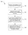
- FIG. 1is a flowchart illustrating the basic method for creating ultra low-k CDO dielectric layers with high hardness/modulus.
- FIG. 2is a graph showing film modulus as a function of film dielectric constant for single precursor ULK materials.
- FIG. 3shows FTIR spectra of a single-precursor as-deposited and post UV cured films.
- FIG. 4is a graph showing pore size distribution of two single precursor ULK films produced, one having a k-value of 2.5 and one having a k-value of 2.7.
- FIG. 5is a graph showing methanol diffusion as a function of pore size.
- FIG. 6is a graph showing hydrocarbon out-gassing of ULK as a function of deposition temperature.
- FIG. 7is mass spectra showing out-gassed species.
- FIG. 8is a simple block diagram depicting various reactor components arranged as in a conventional reactor.
- FIG. 9is an example of UV cure chamber that may be used in accordance with certain embodiments of the invention.
- the present inventionrelates to ultra low-k (ULK) CDO films, with significantly improved chemical and mechanical properties.
- the methods of the inventioninvolve depositing CDO films via plasma enhanced chemical vapor deposition (PECVD) using a precursor having one or more functional groups.
- PECVDplasma enhanced chemical vapor deposition
- UV-assisted Thermal Processing (UVTP)is applied to produce ULK CDO films with desirable chemical bond and structure.
- UVTPincreases cross-linking and lower the dielectric constant of the deposited film.
- CDO filmrefers to a material whose compositional elements include Si, O, C and H, which may be crosslinked to form the CDO matrix. It may contain traces of other elements, including fluorine (F) or germanium (Ge).
- “Ultra low-k”, in the context of this inventionmeans that the dielectric constant of the CDO layer is not greater than about 2.7. In particular embodiments, the CDO layer has a dielectric constant of about 2.5.
- Insulating materials with ultra low dielectric constantsare needed to minimize signal propagation delay, crosstalk and power consumption as inter-metal spacing decreases in advanced integrated interconnects.
- FSGfluorinated silicate glass
- CDO films deposited using PECVDtypically containing only carbon and hydrogen atoms in addition to silicon and oxygen atoms. Because they share many similarities with SiO 2 and FSG in composition and thermo-mechanical properties, PECVD CDO films offers an evolutionary approach to solving the low k IMD challenge.
- the bulk dielectric constant (k) of CDO films being implemented at 90 nmtypically ranges from 3.2 to as low as 2.85, which is significantly lower than those of SiO 2 (k ⁇ 4.1) and FSG (k ⁇ 3.6).
- kthe mechanical properties of dielectric films gradually degrade due to incorporation of more methyl (—CH 3 ) groups and free space.
- Many device failurescan often be ultimately traced to the poor mechanical properties of the CDO films.
- the introduction of more free space, i.e., pores, within the filmcould result in a number of undesirable properties such as a reduction in mechanical strength and penetration of chemicals.
- the gas-phase precursors used during subsequent chemical vapor deposition or atomic layer depositionmay have a tendency to infiltrate the porous dielectric.
- the penetration of metallic species or solvents during integrationcould damage the electric properties of the ULK dielectrics.
- ULK filmshaving good mechanical strength and resistance to penetration by foreign species.
- Current methods of depositing ULK filmstypically require using two precursors—a backbone network former and a porogen.
- the backbone network formeris typically a silicon-containing compound and the porogen a separate organic compound.
- the porogenis typically driven out with a cure process, leaving the backbone behind, thereby creating a porous dielectric film.
- Porogensare typically organic materials such as a polymers that typically exist as a separate phase from the backbone network former within the deposited precursor layer.
- the porogenis such that it is able to be removed from the deposited layer by the application of energy, e.g., heat, plasma, ultra-violet radiation, etc.
- the methods of the present inventionuse a single precursor and hence eliminate the porogen removal step.
- Use of a single precursor and elimination of the porogen removal operationhas advantages in certain applications ⁇ for example, out-gassing of species in the deposited film during subsequent operations is reduced, thereby easing integration.
- the single precursor filmshave improved chemical inertness relative to the dual precursor films as there is no organic porogen in the matrix; porogen-based films may contain unstable organic species that remain in the matrix.
- dual precursor filmsrefers to films deposited with a backbone network former precursor and a porogen precursor as described above).
- the films produced by the methods of the present inventionhave performance comparable to the dual precursor films.
- film having a k-value of 2.5 and a modulus of 7.5 GPacan be achieved using the single precursor methods of the present invention—film performance previously achievable only with the dual precursor methods.
- Hardness and modulusare well defined within the art and will not be discussed in detail herein. Measures of film hardness and modulus presented herein may be made with any suitable apparatus including a nano-indentation device.
- FIG. 1is a flowchart illustrating a high level method for creating ultra low-k CDO dielectric layers with high hardness/modulus. The operations are described briefly here and in further detail below.
- a waferis supplied to a PECVD reactor.
- a single silicon-containing precursoris introduced in a process gas.
- Precursor selectionhas strong effects on the material properties of the film. Generally, precursors are chosen to have a high carbon content and one or more functional groups, including in some embodiments triple bonds.
- the process gasmay also contain an oxidant and typically contains a carrier gas. Precursor selection is described further below.
- a plasmais ignited under conditions that promote incorporation of desired compositional bond structure in the CDO film in an operation 115 .
- Process conditions for the PECVD depositionare described further below.
- UV radiationis typically a UV-assisted thermal processing (UVTP) operation, also discussed further below.
- UV curingis increase mechanical strength, and in certain embodiments, lower the dielectric constant.
- Choice of the CDO precursor(s)is also important to this operation as UV radiation has different effects on different film compositions. For most CDO film compositions and/or under certain UV exposure conditions, dielectric constant may rise as a result of UV curing.
- UV cureis able to lower the k-value of CDO films deposited using certain precursors having carbon-carbon triple bonds, e.g., TMSA and BTMSA, and other functional groups as discussed below.
- Operation 120may occur in the same chamber as the deposition if equipped with a UV source, or the wafer may be transferred to another chamber equipped with a UV source.
- the PECVD/UVTP processmay be repeated to produce an ultra low-k film of a certain thickness in stages.
- the methods of this inventionuse a UV cure process to increase the mechanical strength.
- the UV cure process of the methods of the inventionlowers the dielectric constant.
- dielectric constants lower than or equal to about 2.5may be achieved using the methods of the invention.
- current technology to prepare ULK filmsuses two precursors—a backbone network former and a porogen. The porogen is typically driven out with a cure process, leaving the backbone behind.
- the methods of the present inventionmay be implemented using only a single CDO precursor without the need for a porogen removal step.
- the sp 2 and sp structurescomprise C ⁇ C and C ⁇ C bonds and have significantly different atom-atom of distance than C—C, C—O, Si—O, or Si—C bonds do.
- Nominal bond length of C—C bondis ⁇ 1.5 Angstroms, that of C ⁇ C bond is ⁇ 1.3 Angstroms and that of CC bond is ⁇ 1.2 Angstroms, that of C—O bond is ⁇ 1.1 Angstroms while the nominal bond length of Si—O bond is ⁇ 1.6 Angstroms and that of Si—C bond is ⁇ 1.9 Angstroms. Because of their rigidity and bond lengths, the C ⁇ C or C ⁇ C bonds (and their derivative forms) provide means to alter the Si—O—Si matrix structure and increase the nanometer scale pore space in the CDO matrix.
- Precursors of interestare generally carbon-rich organosilicon compounds containing functional groups such as Si—C x H y (cyclic or linear), Si—C x H y O z (cyclic or linear), Si—CH ⁇ (cyclic or linear) and Si—C ⁇ (cyclic or linear) groups.
- precursors containing triple bondshave been shown to produce ULK films having high modulus according to the methods of the invention.
- Precursors having carbon-carbon triple bondsfound in various classes of compound including, for example, silanes having at least one hydrocarbon group with a carbon-carbon triple bond and at least one alkyl group or at least one oxy-hydrocarbon group, bis(alkylsilyl)acetylenes, bis(alkylsilyl)ethylenes, and siloxanes having pendant hydrocarbon groups with a carbon-carbon triple bond.
- TrimethylsilaneacetyleneSiC 5 H 10 : TMSA, also known as ethynyltrimethylsilane (ETMS), (CH 3 ) 3 Si—C ⁇ C—H
- Methyldimethoxysilaneacetylene(SiC 5 H 11 O 2 ): MDMOSA, (CH 3 O) 2 (CH 3 )Si—C ⁇ CH
- Dimethylethoxysilaneacetylene(SiC 6 H 13 O): DMEOSA, (C 2 H S O)(CH 3 ) 2 Si—C ⁇ CH
- Methyldiethoxysilaneacetylene(SiC 7 H 15 O 2 ): MDEOSA, (C 2 H S O) 2 (CH 3 )Si—C ⁇ CH
- Ethyldiethoxysilaneacetylene(SiC 8 H 17 O 2 ): EDEOSA, (C 2 H S O) 2 (C 2 H 5 )Si—C ⁇ CH
- Dimethylsilane-diacetylene(SiC 6 H 8 ): DMSDA, (CH 3 ) 2 Si(C ⁇ CH) 2
- Methylsilane-triacetylene(SiC 7 H 6 ): MSTA, (CH 3 )Si(C ⁇ CH) 3 ;
- Tetraacetylene Silane(SiC 8 H 4 ): TAS, Si(C ⁇ CH) 4
- the functional groupsare C ⁇ C (triple bonds), which may be pendant or embedded within other functionalities. During deposition, these special functional groups become integrated in the CDO film on the substrate. Rigid C ⁇ C bonds, and their derivative bonding structures through crosslinking with Si, O, and C, when embedded in the CDO film, strengthen the material matrix and alter Si—O—Si backbone structure of CDO films, resulting in a more rigid lattice, thus lowering the tensile stress of the CDO film. As presented below, the incorporation of C ⁇ C and C ⁇ C bond and their derivative forms within the Si—O—Si structure was observed by FTIR and other analytical methods. Such films may be formed from a single organosilicon containing precursor or multiple precursors in combination.
- a single precursorcontains at least one carbon-carbon triple bond.
- the functional groupsare C ⁇ C bonds, contained in a single precursor if used. But if multiple precursors are used in combination, it is not necessary for each of them to include an unsaturated group.
- Various primary precursorsmay be employed which have no double bonds or triple bonds.
- the use of multiple precursorsis distinct from the “dual precursor” ⁇ backbone network former and porogen ⁇ methods used to deposit porous ULK films.
- the methods of the present inventioneliminate the need for a porogen removal operation.
- a single hydrocarbon precursori.e., the organosilicon precursor
- multiple organic precursorse.g., multiple organosilicon precursors none of which is a porogen, may also be used.
- the process gasmay also contain carrier gases and a source of oxygen (the oxygen source may also be used as the carrier gas).
- the carrier gasis provided in much greater volumes than the precursor gases. It is used as a delivery vehicle and a means for sweeping precursor materials and byproducts through the reactor.
- oxygen containing gasessuch as molecular oxygen (O 2 ), ozone (O 3 ), hydrogen peroxide (H 2 O 2 ), nitrous oxide (N 2 O) and carbon dioxide (CO 2 ) may be used.
- Carbon dioxideis preferred for many applications of this invention.
- hydrogenis used as the carrier gas.
- inert gasessuch as helium, argon, nitrogen, etc. are used.
- the process gasemploys a carrier gas but no separate oxygen source (e.g., molecular oxygen, ozone, hydrogen peroxide or carbon dioxide).
- the carrier gasinclude inert gases and hydrogen.
- a single precursorprovides all the necessary oxygen, silicon, and carbon, including the carbon-carbon triple bonds and other functional groups if present.
- siloxanes and various silanes or compounds having silyl groups with hydrocarbon oxy moietiesare suitable for this purpose.
- precursors that may be used in such process gasesare POTMS, DTDS, DMMOSA, MDMOSA, DMEOSA, MDEOSA and EDEOSA.
- the carrier gassupplies some or all of the oxygen.
- suitable oxygenated carrier gasesare carbon dioxide, ozone, hydrogen peroxide, molecular oxygen or other oxygen containing molecules.
- a single precursoris employed. It may or may not include oxygen. In cases where no oxygen is used, it could simply be a hydrocarbon silane material involving one carbon-carbon triple bond.
- suitable precursors for this embodimentinclude ETMS or TMSA, PTMS, BTMSA, TAS, MSTA, MDEOSA, DMEOSA, DMSDA and VTMS. Any one of these single precursors may be used in conjunction with a carrier gas.
- oxygenis again supplied in a carrier gas such as carbon dioxide, oxygen, ozone, nitrous oxide, or hydrogen peroxide.
- a carrier gassuch as carbon dioxide, oxygen, ozone, nitrous oxide, or hydrogen peroxide.
- two or more precursorsare employed. At least one of these may be similar to those identified in the second example.
- some amount of oxygenmay be present in one or more of these molecules.
- Many relatively simple hydrocarbon silanes and/or silyl compoundsmay be employed as the primary precursor.
- the process gasincludes a carrier gas, an optional oxidant(s) (if not included in the carrier gas or the silicon-containing precursor) and the desired silicon and organic functional groups in one or more precursors.
- the process gasconsists essentially of a carrier gas of CO 2 and inert gas (e.g., CO 2 +He), a small amount of oxygen and a single organic precursor.
- the process gasemploys a single silicon-containing precursor in addition to the carrier gas and an optional oxidant, e.g., the process gas may consist essentially of a silicon-containing precursor that also contains the desired functional group(s), an optional oxidant (if necessary) and a carrier gas.
- the process gascomprises a silicon-containing precursor that also contains a carbon-carbon triple bond, an optional oxidant, and a carrier gas.
- the process gasmay consist essentially of these gases.
- Particular examplesinclude TMSA/oxidant/carrier gas and BTMSA/oxidant/carrier gas.
- the carrier gasmay include the oxidant.
- the methods of the inventionproduce ULK films deposited using a single precursor that have properties comparable to porous ULK films deposited using dual (backbone and porogen) precursors.
- CDO dielectric materials of this inventionmay be employed to form various deposition techniques. These include various other forms of chemical vapor deposition (CVD) including plasma enhanced CVD (PECVD) and high-density plasma CVD (HDP CVD). HDP CVD of dielectric materials is described in various sources including U.S. Pat. No. 6,596,654, which is incorporated herein by reference for all purposes. Additionally, other techniques such as spin on techniques and deposition from supercritical solutions may be employed. But for many applications of this invention, a plasma based CVD process is employed.
- CVDchemical vapor deposition
- PECVDplasma enhanced CVD
- HDP CVDhigh-density plasma CVD
- the deposition conditionsmay be optimized to promote the crosslinking of incorporated bonds. Without this crosslinking, the film mechanical strength will generally be low due to the fact that an increase in content of methyl group CH 3 as a terminating group in the CDO film will reduce the bonding density per volume thus the bonding integrity of the film. With crosslinking, the Si—O—Si matrix structure is strengthened. As a result, the mechanical strength, or the fracture toughness, of the as deposited CDO film will be high.
- Compositional bonds formed in CDO film of particular interest to this inventioninclude Si—CH 2 —Si, Si—C ⁇ C—Si, Si—CH ⁇ CH—S 1 , Si—CH 2 —CH 2 —Si and other derivatives of these bonds due to Si, C or O crosslinking, such as Si—O—C ⁇ C—Si, Si—O—CH ⁇ CH—Si, Si—C(—H, —OSi)—CH 2 —Si, etc. It is noted that the chemical bond length and angle varies with the degree of saturation and crosslinking.
- Nominal bond length of the C—C bondis ⁇ 1.5 ⁇ , that of the C ⁇ C bond is ⁇ 1.3 ⁇ , that of the CC bond is ⁇ 1.2 ⁇ , and that of the C—O bond is ⁇ 1.1 ⁇ while the nominal bond length of the Si—O bond is ⁇ 1.6 ⁇ and that of the Si—C bond is ⁇ 1.9 ⁇ .
- the incorporation of C ⁇ C bond and its derivatives (C ⁇ C, C—C) and their crosslinking within the CDO filmwill greatly influence the Si—O—Si matrix structure. More specifically, the Si—O—Si bond angle will change significantly as the desired C related bonds are incorporated and crosslinked. Since the Si—O—Si matrix is the backbone structure of the CDO film, the change in Si—O—Si bond angle will increase the nanometer scale pore space in the matrix and thereby decrease the dielectric constant in the matrix.
- Residual stresscan be reduced by incorporating C ⁇ C bonds and its derivatives and promoting cross-linking/bridging in the CDO film.
- one methodis to increase ion bombardment during the PECVD deposition.
- Process conditions that increase ion bombardmentmay be chosen to increase one or both of (a) the mean energy of ion striking the substrate and (b) the flux of ions reaching the substrate. Physically, these results may be achieved by selecting process conditions that accomplish one of the following: (i) increasing the mean free path of the ions in the plasma, (ii) reducing the distance that an ion must travel before striking the substrate, and (iii) increasing the mean energy or momentum of the ions that strike the substrate surface.
- At least two different process conditionsmay be manipulated.
- high frequency components of the RF power delivered to a reactorcontrol the plasma density and low frequency components produce ion bombardment of the film.
- the high and low frequency componentscan be provided at any of a number of suitable frequencies.
- the LF componentis provided in a frequency range of about 100 to 600 kHz, more preferably about 200-500 kHz, for example about 300 kHz.
- the High Frequency HF componentis generally between 2-60 MHz ⁇ in one process example, an HF frequency of 13.156 MHz is used.
- the low frequency component of delivered RF poweris between about 0 and 90 percent of the total power, and more preferably between about 0 and 60 percent of the total power (e.g., between about 5 and 40 percent).
- the optimal valuewill vary depending upon the mean free path of the ions and the various conditions that impact mean free path.
- the total power deliveredis about 800 Watts on 6 200 mm wafers or 0.42 W/cm 2 in area density. This value can be varied depending upon the specific application and plasma reactor employed.
- the low frequency componenthas a power area density of between about 0 W/cm 2 and 20 W/cm 2 , and more preferably between 0 W/cm 2 and 1 W/cm 2 .
- the HFRF powermay be pulsed at a certain duty cycle, for example pulsing at between 500 Hz and 10 kHz and varying the HFRF duty cycle from 20-80%. This effectively superimposes a low frequency component on the plasma generation power.
- Another method that may be used to increase ion bombardment during film depositionis to alter the deposition pressure. This simply increases the mean free path of ions in the deposition chamber.
- the deposition pressureis maintained at a pressure of between about 0.5 to 20 Torr, more preferably in the range of about 2-10 Torr.
- Still another adjustment that may be usedinvolves varying the gap between the two capacitor plates of the plasma reactor. In the apparatus described below, this involves choosing an appropriate gap between the showerhead (one capacitor plate) and a thermal block (a second capacitor plate) on which the wafer is positioned, thereby reducing the distance between the plasma source and the substrate. This reduces the distance that an ion must travel before striking the substrate.
- the ideal gapdepends on the type of reactor employed and the process conditions. For many situations, the gap is preferably between about 3 and 20 millimeters.
- Process optimizationalso includes setting the proper flow rates of the various compounds in the process gases.
- the flow ratesare chosen depending upon the amount of surface area to be covered.
- the total precursor flow ratewas 0.5 ml/min to about 10 ml/min. Note that this comprises the total flow rate of all precursors.
- the deposition temperaturecan be tailored to meet the application. For some IC fabrication applications involving copper lines, for example, temperatures below 425 C may be required for intermetal dielectric deposition. In some embodiments, the substrate temperature is maintained between about 300 and 425 C (preferably between about 300 and 350 C) during CDO film deposition.
- the UV source employedmay be of any type, including lasers and lamps.
- lampsinclude a mercury lamp and a xenon arc lamp. These generally emit UV radiation over a relatively wide range of wavelengths.
- Laserstypically emit UV radiation at a single wavelength or a very narrow band of wavelengths. Examples of lasers include excimer lasers and tunable variations.
- the UV radiationshould be directed onto the wafer.
- Various lenses, filters, and other optical elementsmay be employed for this purpose. In some embodiments, the optical elements will expand a beam of UV light to cover an entire wafer.
- the UV radiationwill form a line or patch that illuminates only a portion of the wafer.
- the light and the wafercan be moved with respect to one another to ensure that the whole wafer surface is illuminated over a relatively short period of time.
- a thin strip of light from a laser or other sourceis directed onto the wafer. Then the wafer and the strip of light are moved with respect to one another to ensure that the entire wafer is illuminated.
- temperatures below about 450 degrees C.are preferable, more preferably ⁇ 400 degrees C., as higher temperatures can damage a partially fabricated device, particularly one that employs copper lines.
- Typical temperaturesrange between about room temperature (i.e., 20 degrees C.) up to 450 degrees C., and typically between about 25° C. to 450 C. It should be noted that exposure to UV radiation can itself contribute to substrate heating.
- Chamber pressuresalso can range broadly depending on the precursor and the nature of the UV treatment. For example, appropriate pressures may span a range of between about 10 ⁇ 6 Torr (high vacuum) to 1000 Torr. In the higher pressure ranges, it is important to ensure that moisture, oxygen, or any other undesirable species is kept out of the chamber, with the exception of processes that may want ozone or excited oxygen. In a particular pressure range when using inert gas, the pressure ranges from about 1 mTorr to 100 Torr.
- UV exposure timeis largely a function of both the lamp intensity and thickness of the precursor layer, as well as the desired modulus.
- Lamp intensitiesrange from about 1 mW/cm 2 -50 mW/cm 2 (with 50 mW/cm 2 at about 100% intensity).
- curing timesmay range from about 1-10 minutes, e.g., about 3 minutes, at 100% UV intensity.
- a typical 3 minute cure process for a 2 k ⁇ filmwill result in a modulus of about 10 GPa.
- the UV curelowers the dielectric constant, e.g., by increasing the amount of Si—CH 2 —Si and Si—CH 3 but overexposure will result in higher dielectric constants because of reduction of Si—CH 3 .
- shorter exposure timesare preferred. In a preferred embodiment, the exposure time ranges from about 1 second up to 5 minutes, e.g., 1-2 minutes.
- dielectric constantit desirable to have low dielectric constant without sacrificing mechanical strength.
- One approach to reducing the dielectric constantis to introduce more free space (pores) within the film; however, at a certain point, the introduction of too many pores results undesirable properties such as a reduction in mechanical strength and penetration of chemicals.
- dielectric constantis a function of the degree of dipolarization.
- the dielectric constantis a frequency-dependent, intrinsic material property.
- the constantcan be contributed from three components that result from electronic, ionic and dipolar contributions.
- Si—CH 3 and Si—CH 2 —Si bondsterminate the O—Si—O bonding network, causing a decrease in film density.
- Si—CH 3 and Si—CH 2 —Sireduce the ionic and dipolar contributions to lower the dielectric constant.
- dielectric constantdecreases with increasing Si—CH 3 and Si—CH 2 —Si content.
- UV curingimproves cross-linking and lowers the dielectric constant, producing ULK films that have high mechanical strength. This is significant as UV curing does not lower the dielectric constant for all materials ⁇ for materials with different bonding structures, the dielectric constant would be raised by the application of UV radiation. Reduced dielectric constant is observed for the particular precursors described above, e.g., organosilicon precursors having carbon-carbon triple bonds. It is believed that this is due to several factors. First, there is an increase in free space and pore size due to UV cure. In particular, an increase in pore size from about 1.0 nm to about 1.27 nm is observed for a film deposited using TMSA. Pore size is believed to increase from the conversion of Si—CH 3 groups.
- TMSA-based filmsfor example, some of the deposited Si—CH 3 bonds are cross-linked to form Si—CH 2 —Si, which is believed to the lower the dielectric constant by enlarging the pore size.
- TMSASi—C ⁇ functional group
- some CCmay remain in OSG matrix that can be removed by UV treatment, creating more free space.
- a certain amount of cyclopentene remaining in OSG matrixmay be removed by UV treatment; in depositing phenoxytrimethylsilane (Si—C x H y O z functional group) may be removed by UV treatment; and in depositing phenyldimethylethoxysilane (Si—C ⁇ ), some phenyl groups may remain in OSG matrix that can be removed by UV treatment.
- the methods of the inventionmay be used to fabricate ULK CDO films having k values of between about 2.5 and 2.7, e.g., about 2.5, 2.55, 2.6, 2.65 and 2.7.
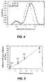
- FIG. 2presents film modulus as a function of k value for single-precursor based dense films deposited by PECVD and cured by UVTP in accordance with a method of the invention.
- a TMSA, CO 2 and O 2 process gaswas used, followed by a UVTP process using 80-100% UV intensity and a substrate temperature of 360-400 C.
- the filmswere exposed to the UV radiation for times ranging from 3-30 minutes depending on film thickness.
- Films ranging with dielectric constants between about 2.5 and 2.75 and modulus between about 7.5 and 12 GPacan be achieved using the methods of the present invention as shown in FIG. 2 . Also as observed, modulus increases with the dielectric constant. However, at a dielectric constant of 2.5, modulus of 7.5 GPa can be achieved—film performance is comparable to that of dual precursor ULK methods.
- FIG. 3shows FTIR spectra of the single-precursor, k of 2.5 film with a spectral comparison of the as-deposited and post UV cured in the range of 1325-1475 cm ⁇ 1 (inset).
- the spectrawere normalized by film thickness.
- the absorption at 1359 cm ⁇ 1is assigned to the bonding of C—H in Si—CH 2 —Si crosslinks while the absorption at 1411 cm ⁇ 1 is assigned to the bending of C—H in Si(CH 3 ) x as shown inset of FIG. 3 .
- Pore size of the films produced by methods of the inventiontypically range from about 0.75-1.75 nm in diameter, with average pore size between about 1.15-1.27 nm in diameter.
- dielectric constantis related to the porosity of the film, including pore size.
- FIG. 4shows pore size distributions for two films produced by methods of the invention using TMSA as a precursor, one having a k of 2.5 and one having a k of 2.7 as measured by a Positronium Annihilation Lifetime Spectroscopy (PALS) analysis.
- PALSPositronium Annihilation Lifetime Spectroscopy
- the film having a k of 2.5has larger pores, with a peak in the distribution of about 1.27 nm compared to the peak of the k2.7 film of about 1.15 nm. Without UV curing, the distribution peaks at about 1.0 nm.
- the methods of the present inventionproduce films having zero interconnectivity.
- Interconnectivityrefers to the degree to which the pores are interconnected.
- porogen-based filmshave high interconnectivity (typical interconnectivities of porogen-based films range from about 5-20 nm) while films of the produced by the PECVD/UVTP methods described herein have zero interconnectivity as measured by a PALS analysis of the low-k films.
- the films produced by the methods of the inventionalso have lower average pore size, with average pore size of porogen-based films around 1.5 nm. Zero interconnectivity and lower pore size results in mechanically stronger films, as well as low diffusion coefficients, as explained below.
- the ULK films of the present inventionhave low diffusion coefficients. This is due to several factors.
- the films of the present inventionare closed pore (zero interconnectivity). Porogen based processes of producing ULK films may produce open pore films with channels that connect pores. The films also have smaller pores.
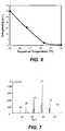
- FIG. 5is a graph showing methanol diffusion as a function of pore size.
- Reference number 501indicates dense CDO film (HM-Coral)
- reference number 503indicates k2.7 film produced by a PECVD/UVTP method
- reference number 505indicates k2.5 film produced by a PECVD/UVTP method
- reference number 507indicates k2.5 film deposited by a dual precursor porogen-based process.
- the SP-ULK filmhas a higher diffusion coefficient than that of the denser films. However, it favorably compares to the dual precursor film having the same dielectric constant.
- FIG. 6shows out-gassing as a function of deposition temperature for ULK films formed by single precursor PECVD/UVTP methods (out-gassing was measured subsequent to deposition and cure). As shown in the figure, large decreases in hydrocarbon out-gassing were observed for films deposited at higher temperatures. Very little or no out-gassing was observed for the single precursor CDO films deposited at 350-400 C was observed.
- FIG. 7is a mass spectra showing the out-gassed species.
- the methods of the inventionmay be used to deposit CDO films having various dielectric constants, e.g., ranging from 2.5 to 2.7.
- An example of a single precursor process gas and conditions that may be used to deposit a film having k2.5 and a film having k2.7follow:
- k-valuemay be controlled in part by adjusting the flow rate of precursor used, with high TMSA flow resulting a lower k-value.
- the apparatuswill include one or more chambers or “reactors” (sometimes including multiple stations) that house one or more wafers and are suitable for wafer processing.
- Each chambermay house one or more wafers for processing.
- the one or more chambersmaintain the wafer in a defined position or positions (with or without motion within that position, e.g. rotation, vibration, or other agitation).
- a wafer undergoing dielectric depositionis transferred from one station to another within the reactor during the process. While in process, each wafer is held in place by a pedestal, wafer chuck and/or other wafer holding apparatus.
- the apparatusmay include a heater such a heating plate.
- a PE-CVD (Plasma Enhanced Chemical Vapor Deposition) systemmay be used as well as, for example, an HDP CVD (High Density Plasma Chemical Vapor Deposition) system.
- FIG. 8provides a simple block diagram depicting various reactor components arranged for implementing the present invention.
- a reactor 800includes a process chamber 824 , which encloses other components of the reactor and serves to contain the plasma generated by a capacitor type system including a showerhead 814 working in conjunction with a grounded heater block 820 .
- a high-frequency RF generator 802 and a low-frequency RF generator 804are connected to a matching network 806 that, in turn is connected to showerhead 814 .
- the power and frequency supplied by matching network 806is sufficient to generate a plasma from the process gas, for example 800 W total energy.
- a wafer pedestal 818supports a substrate 816 .
- the pedestaltypically includes a chuck, a fork, or lift pins to hold and transfer the substrate during and between the deposition reactions.
- the chuckmay be an electrostatic chuck, a mechanical chuck or various other types of chuck as are available for use in the industry and/or research.
- the process gasesare introduced via inlet 812 .
- Multiple source gas lines 810are connected to manifold 808 .
- the gasesmay be premixed or not.
- Appropriate valving and mass flow control mechanismsare employed to ensure that the correct gases are delivered during the deposition and plasma treatment phases of the process.
- liquid flow control mechanismsare employed. The liquid is then vaporized and mixed with other process gases during its transportation in a manifold heated above its vaporization point before reaching the deposition chamber.
- a vacuum pump 826e.g., a one or two stage mechanical dry pump and/or a turbomolecular pump typically draws process gases out and maintains a suitably low pressure within the reactor by a close loop controlled flow restriction device, such as a throttle valve or a pendulum valve.
- FIG. 9is a schematic diagram of an example UVTP chamber 901 in accordance with the invention.
- Chamber 901is capable of holding a vacuum and/or containing gases at pressures above atmospheric pressure. For simplicity, only one chamber 901 is shown. It is noted that in many embodiments, chamber 901 is one chamber in a multi-chambered apparatus (entire apparatus not shown), although chamber 901 could alternatively be part of a stand-alone single chambered apparatus. Suitable multi-chambered apparatus, for example, include the modified Novellus Sequel and Vector systems.
- a substrate holder 903secures a wafer 905 in a position such that light from a UV light source array 907 can irradiate wafer 905 .
- Substrate holder 903can have a heater (not shown) that can heat the substrate to defined temperatures, or could be cooled using a chiller and can be controlled by a temperature controller (not shown).
- Chamber 901is configured with a gas inlet 915 , which is connected to a gas source (not shown), and with a vacuum outlet 913 , which is connected to a vacuum pump (not shown). The amount of gas introduced into the chamber 901 can be controlled by valves and mass flow controller (not shown) and pressure is measured by pressure gauge (not shown).
- UV light source array 907is mounted outside the chamber 901 . In alternate embodiments, the UV light source array may be housed inside the chamber 901 .
- UV light source array 907includes an array of individual UV sources such as mercury vapor or xenon lamps. Note that the invention is not limited to mercury vapor or xenon lamps as UV light sources and other suitable light sources include deuterium lamps or lasers (e.g., excimer lasers and tunable variations of various lasers). Various optical elements, such as reflectors, may be required to direct the UV light toward portions of the substrate. Methods for directing the light at different portions of the substrate at different times may be required as well. A scanning mechanism may be used for this purpose.
- a window 911 made of quartz, sapphire or other suitable materialis positioned between UV light source array 907 and wafer 905 to provide vacuum isolation. Filters can also be used to remove unwanted spectral components from particular sources to “tune” the sources.
- the UV light source array 907may be comprised of one or more types of UV sources, for example an array of three types of UV sources, each type providing UV radiation with a different wavelength distribution.
- the UV sourcesare electrically connected to each other ( 909 a , 909 b and 909 c ) and controlled by control system 910 , which controls when each of the various UV sources is illuminated.
- Control system 910is typically, but not limited to, a computer processing system such as a PC or workstation. Of course, any number and types of individual light sources in any suitable configuration can be used.
- the light source array and control configuration of FIG. 9is only an example of a suitable configuration.
- the lampsare arranged to provide uniform UV radiation to the wafer.
- other suitable lamp arrangementscan include circular lamps concentrically arranged or lamps of smaller length arranged at 90 degree and 180 degree angles with respect to each other may be used.
- the light source(s)can be fixed or movable so as to provide light in appropriate locations on the wafer.
- an optical systemincluding for example a series of movable lenses, filters, and/or mirrors, can be controlled to direct light from different sources to the substrate at different times.
- the UV light intensitycan be directly controlled by the type of light source and by the power applied to the light source or array of light sources. Factors influencing the intensity of applied power include, for example, the number or light sources (e.g., in an array of light sources) and the light source types (e.g., lamp type or laser type). Other methods of controlling the UV light intensity on the wafer sample include using filters that can block portions of light from reaching the wafer sample. As with the direction of light, the intensity of light at the wafer can be modulated using various optical components such as minors, lenses, diffusers and filters.
- the spectral distribution of individual sourcescan be controlled by the choice of sources (e.g., mercury vapor lamp vs. xenon lamp vs. deuterium lamp vs. excimer laser, etc.) as well as the use of filters that tailor the spectral distribution. In addition, the spectral distributions of some lamps can be tuned by doping the gas mixture in the lamp with particular dopants such as iron, gallium, etc.
- FIG. 9is only an example of a suitable apparatus and other designs for other methods involved in previous and/or subsequent processes may be used.
- Other examples of apparatus suitable for implementing the present inventionare described in commonly assigned co-pending application Ser. Nos. 11/115,576 filed Apr. 26, 2005, 10/800,377 filed Mar. 11, 2004, and 10/972,084 filed Oct. 22, 2004, incorporated by reference herein.
Landscapes
- Engineering & Computer Science (AREA)
- Chemical & Material Sciences (AREA)
- Physics & Mathematics (AREA)
- Manufacturing & Machinery (AREA)
- General Physics & Mathematics (AREA)
- Computer Hardware Design (AREA)
- Microelectronics & Electronic Packaging (AREA)
- Power Engineering (AREA)
- Condensed Matter Physics & Semiconductors (AREA)
- Chemical Kinetics & Catalysis (AREA)
- General Chemical & Material Sciences (AREA)
- Materials Engineering (AREA)
- Mechanical Engineering (AREA)
- Metallurgy (AREA)
- Organic Chemistry (AREA)
- Inorganic Chemistry (AREA)
- Plasma & Fusion (AREA)
- Formation Of Insulating Films (AREA)
- Internal Circuitry In Semiconductor Integrated Circuit Devices (AREA)
Abstract
Description
This invention relates to methods for preparing dielectric films having low dielectric constants and high mechanical strength.
There is a general need for materials with low dielectric constants (low-k) in the integrated circuit manufacturing industry. Using low-k materials as the interlayer dielectric of conductive interconnects reduces the delay in signal propagation and signal crosstalk due to capacitive effects. The lower the dielectric constant of the dielectric, the lower the capacitance of the dielectric and the RC delay in the lines and signal crosstalk between electrical lines of the IC. Further, the use of low k materials as interlayer dielectrics will reduce power consumption of complex integrated circuits.
Low-k dielectrics are conventionally defined as those materials that have a dielectric constant (k) lower than that of silicon dioxide (SiO2), that is k<˜4. Generally, they have a dielectric constant of 3 or less. Typical methods of obtaining low-k materials include introducing pores into the dielectric matrix and/or doping silicon dioxide with various hydrocarbons or fluorine. In technology nodes of 90 nanometers and beyond (e.g., 65 nanometers), carbon doped oxide dielectric materials look extremely promising. However, wide spread deployment of these materials in modern integrated circuit fabrication processes is hindered by increasing demands for high mechanical strength coupled with lower dielectric constants. For certain applications, it is now necessary to use dielectric materials having k values below about 2.7.
The International Technology Road Map for Semiconductors (ITRS) specifies that materials with dielectric constants (k) of 2.4 to 2.7 will be required for the 45 nm technology node. Plasma Enhanced Chemical Vapor Deposition (PECVD) carbon doped silicon oxide (CDO) is used for 90 nm and 65 nm technology nodes with k ranging between 2.8 and 3.2. Further reduction of the dielectric constant to below 2.7 is achievable through incorporation of additional methyl groups and/or free space. Typically, this is accomplished through co-deposition of a backbone precursor and a porogen. The porogen is driven out during a cure step, leaving the backbone and increased free space behind. This free space can lead to degraded mechanical properties of the film relative to fully dense materials. It also allows penetration of moisture and solvents during integration, potentially lowering the interconnect performance.
The present invention provides methods of preparing low-k carbon-doped oxide (CDO) films having high mechanical strength. The methods involve contacting the substrate with a CDO precursor to deposit the film typically using a plasma-enhanced chemical vapor deposition (PECVD) method. After the film is deposited, it is exposed to ultraviolet radiation in a manner that increases cross-linking and/or lowers the dielectric constant of the film. The resulting films have ultra-low dielectric constants, e.g., about 2.5, but also high mechanical strength, e.g., a modulus of at least about 7.5 GPa. In certain embodiments, a single hydrocarbon precursor is used, resulting in an improved process for obtaining ULK films that does not require dual (porogen and backbone) precursors.
These and other features and advantages of the invention will be presented in more detail below with reference to the associated drawings.
The present invention relates to ultra low-k (ULK) CDO films, with significantly improved chemical and mechanical properties. The methods of the invention involve depositing CDO films via plasma enhanced chemical vapor deposition (PECVD) using a precursor having one or more functional groups. UV-assisted Thermal Processing (UVTP) is applied to produce ULK CDO films with desirable chemical bond and structure. In specific embodiments, the UVTP increases cross-linking and lower the dielectric constant of the deposited film.
Generally, CDO film refers to a material whose compositional elements include Si, O, C and H, which may be crosslinked to form the CDO matrix. It may contain traces of other elements, including fluorine (F) or germanium (Ge). “Ultra low-k”, in the context of this invention means that the dielectric constant of the CDO layer is not greater than about 2.7. In particular embodiments, the CDO layer has a dielectric constant of about 2.5.
Insulating materials with ultra low dielectric constants are needed to minimize signal propagation delay, crosstalk and power consumption as inter-metal spacing decreases in advanced integrated interconnects. In order to meet these escalating performance demands, the industry has begun to replace SiO2and fluorinated silicate glass (FSG) with alternative dielectrics in full-scale production at the 90 nm and 65 nm technology nodes with CDO films deposited using PECVD, typically containing only carbon and hydrogen atoms in addition to silicon and oxygen atoms. Because they share many similarities with SiO2and FSG in composition and thermo-mechanical properties, PECVD CDO films offers an evolutionary approach to solving the low k IMD challenge.
The bulk dielectric constant (k) of CDO films being implemented at 90 nm typically ranges from 3.2 to as low as 2.85, which is significantly lower than those of SiO2(k˜4.1) and FSG (k˜3.6). As the k value lowers, the mechanical properties of dielectric films gradually degrade due to incorporation of more methyl (—CH3) groups and free space. Many device failures can often be ultimately traced to the poor mechanical properties of the CDO films. The introduction of more free space, i.e., pores, within the film could result in a number of undesirable properties such as a reduction in mechanical strength and penetration of chemicals. The gas-phase precursors used during subsequent chemical vapor deposition or atomic layer deposition may have a tendency to infiltrate the porous dielectric. The penetration of metallic species or solvents during integration could damage the electric properties of the ULK dielectrics.
The challenge then is to create ultra-low k films having good mechanical strength and resistance to penetration by foreign species. Current methods of depositing ULK films typically require using two precursors—a backbone network former and a porogen. The backbone network former is typically a silicon-containing compound and the porogen a separate organic compound. The porogen is typically driven out with a cure process, leaving the backbone behind, thereby creating a porous dielectric film. Porogens are typically organic materials such as a polymers that typically exist as a separate phase from the backbone network former within the deposited precursor layer. The porogen is such that it is able to be removed from the deposited layer by the application of energy, e.g., heat, plasma, ultra-violet radiation, etc.
In certain embodiments, the methods of the present invention use a single precursor and hence eliminate the porogen removal step. Use of a single precursor and elimination of the porogen removal operation has advantages in certain applications˜for example, out-gassing of species in the deposited film during subsequent operations is reduced, thereby easing integration. In addition, the single precursor films have improved chemical inertness relative to the dual precursor films as there is no organic porogen in the matrix; porogen-based films may contain unstable organic species that remain in the matrix. (For purposes of discussion, dual precursor films refers to films deposited with a backbone network former precursor and a porogen precursor as described above).
Importantly, the films produced by the methods of the present invention have performance comparable to the dual precursor films. For example, film having a k-value of 2.5 and a modulus of 7.5 GPa can be achieved using the single precursor methods of the present invention—film performance previously achievable only with the dual precursor methods. (Hardness and modulus are well defined within the art and will not be discussed in detail herein. Measures of film hardness and modulus presented herein may be made with any suitable apparatus including a nano-indentation device.)
PECVD processes for producing high quality, low-k films with high mechanical strength using precursors having unsaturated bonds is discussed in the following commonly-assigned U.S. patent applications, which are hereby incorporated by reference in their entireties and for all purposes: U.S. patent application Ser. Nos. 10/789,103 and 10/820,525, both titled “METHODS FOR PRODUCING LOW-K CDO FILMS WITH LOW RESIDUAL STRESS”; U.S. patent application Ser. No. 10/800,409, titled METHODS FOR PRODUCING LOW-K CDO FILMS; and U.S. patent application Ser. No. 10/941,502, titled “METHODS FOR IMPROVING INTEGRATION PERFORMANCE OF LOW STRESS CDO FILMS.” The methods of this invention use a UV cure process to increase the mechanical strength. In addition to increasing the mechanical strength of the film, in certain embodiments, the UV cure process of the methods of the invention lowers the dielectric constant. In certain embodiments, dielectric constants lower than or equal to about 2.5 may be achieved using the methods of the invention. As indicated above, current technology to prepare ULK films uses two precursors—a backbone network former and a porogen. The porogen is typically driven out with a cure process, leaving the backbone behind. The methods of the present invention may be implemented using only a single CDO precursor without the need for a porogen removal step.
As discussed in above-referenced U.S. patent application Ser. No. 10/800,409, it has been found that rigid chemical bonds such as carbon-carbon triple bonds strengthen a solid's matrix and generate additional free space (a nanometer scale pore space), thereby lowering the k value of the solid's dielectric constant. The advantages gained by introducing these unsaturated groups can be understood as follows. There are four major structural configurations for carbon in CDO films. The tetrahedral sp3structure has the most degrees of freedom while the other three structures (the triangular sp2structure and linear sp structures —C≡ and ═C═) have fewer degrees of freedom and thus have more rigidity. Due to the reactive nature of deposition process and carbon-carbon triple bonds, not only triple bonds themselves but also their derivative forms will be present in CDO films. These derivative forms result from the opening of one or two of the triple bond to form carbon-carbon double bond or carbon-carbon bond, and/or crosslinking to Si—O—Si network. The sp2and sp structures comprise C═C and C≡C bonds and have significantly different atom-atom of distance than C—C, C—O, Si—O, or Si—C bonds do. Nominal bond length of C—C bond is ˜1.5 Angstroms, that of C═C bond is ˜1.3 Angstroms and that of CC bond is ˜1.2 Angstroms, that of C—O bond is ˜1.1 Angstroms while the nominal bond length of Si—O bond is ˜1.6 Angstroms and that of Si—C bond is ˜1.9 Angstroms. Because of their rigidity and bond lengths, the C═C or C≡C bonds (and their derivative forms) provide means to alter the Si—O—Si matrix structure and increase the nanometer scale pore space in the CDO matrix.
The deposition of CDO films using certain precursors containing unsaturated bonds results in low k films that also have high mechanical strength. It has been found that the addition of a post-deposition UVTP operation to the PECVD process described in that application improves cross-linking (thereby improving hardness and modulus) and lowers the dielectric constant.
Precursor Optimization
Both process optimization and precursor selection can have strong effects on the material properties of the film. Precursors of interest are generally carbon-rich organosilicon compounds containing functional groups such as Si—CxHy(cyclic or linear), Si—CxHyOz(cyclic or linear), Si—CH═ (cyclic or linear) and Si—C≡ (cyclic or linear) groups. In particular, precursors containing triple bonds have been shown to produce ULK films having high modulus according to the methods of the invention.
Precursors having carbon-carbon triple bonds found in various classes of compound including, for example, silanes having at least one hydrocarbon group with a carbon-carbon triple bond and at least one alkyl group or at least one oxy-hydrocarbon group, bis(alkylsilyl)acetylenes, bis(alkylsilyl)ethylenes, and siloxanes having pendant hydrocarbon groups with a carbon-carbon triple bond.
Several silicon-containing, C≡C containing, hydrocarbons (with or without oxygen) have been identified as precursors that may be used in a deposition process to form CDO films having low dielectric constants. These include the following:
Trimethylsilaneacetylene (SiC5H10): TMSA, also known as ethynyltrimethylsilane (ETMS), (CH3)3Si—C≡C—H
Propargyltrimethylsilane (SiC6H12): PTMS, (CH3)3Si—CH2—C≡C—H
Propargyloxytrimethylsilane (SiC6H12O): POTMS, (CH3)3Si—O—CH2—C═C—H
Bis(trimethylsilyl)acetylene (Si2C8H18): BTMSA, (CH3)3Si—C≡C—Si(CH3)3
1,3-Diethynyltetramethyldisiloxane (Si2C8H14O): DTDS, HC═C—Si(CH3)2—O—Si(CH3)2—C≡C—H
Dimethylmethoxysilaneacetylene (SiC5H11O): DMMOSA, (CH3O)(CH3)2Si—C≡CH
Methyldimethoxysilaneacetylene (SiC5H11O2): MDMOSA, (CH3O)2(CH3)Si—C≡CH
Dimethylethoxysilaneacetylene (SiC6H13O): DMEOSA, (C2HSO)(CH3)2Si—C≡CH
Methyldiethoxysilaneacetylene (SiC7H15O2): MDEOSA, (C2HSO)2(CH3)Si—C≡CH
Ethyldiethoxysilaneacetylene (SiC8H17O2): EDEOSA, (C2HSO)2(C2H5)Si—C≡CH
Dimethylsilane-diacetylene (SiC6H8): DMSDA, (CH3)2Si(C≡CH)2
Methylsilane-triacetylene (SiC7H6): MSTA, (CH3)Si(C≡CH)3; and
Tetraacetylene Silane (SiC8H4): TAS, Si(C≡CH)4
The functional groups are C≡C (triple bonds), which may be pendant or embedded within other functionalities. During deposition, these special functional groups become integrated in the CDO film on the substrate. Rigid C≡C bonds, and their derivative bonding structures through crosslinking with Si, O, and C, when embedded in the CDO film, strengthen the material matrix and alter Si—O—Si backbone structure of CDO films, resulting in a more rigid lattice, thus lowering the tensile stress of the CDO film. As presented below, the incorporation of C═C and C≡C bond and their derivative forms within the Si—O—Si structure was observed by FTIR and other analytical methods. Such films may be formed from a single organosilicon containing precursor or multiple precursors in combination. If a single precursor is used, then it contains at least one carbon-carbon triple bond. Also, in certain embodiments, the functional groups are C═C bonds, contained in a single precursor if used. But if multiple precursors are used in combination, it is not necessary for each of them to include an unsaturated group. Various primary precursors may be employed which have no double bonds or triple bonds.
It should be noted that the use of multiple precursors is distinct from the “dual precursor”˜backbone network former and porogen˜methods used to deposit porous ULK films. As noted above, in certain embodiments, the methods of the present invention eliminate the need for a porogen removal operation. In some cases, a single hydrocarbon precursor (i.e., the organosilicon precursor) is used in the process gas. In certain embodiments, however, multiple organic precursors (e.g., multiple organosilicon precursors) none of which is a porogen, may also be used.
Examples of precursors having Si—CxHyand/or Si—CxHyOzand/or Si—CH=functional groups include 3-(trimethylsilyl)cyclopentene, 1,3-Divinyltetramethyldisiloxane (Si2C8H18O): DVDS, H2C═CH—Si(CH3)2—O—Si(CH3)2—CH═CH2, Vinylmethyldimethoxysilane (SiC5H12O2): VMDEOS, (CH3O)2(CH3)Si—CH═CH2, Divinyldimethylsilane (SiC6H12): DVDMS, (CH3)2Si(CH═CH2)2, Phenoxytrimethylsilane and Phenyldimethylethoxysilane.
In addition to the CDO precursor(s), the process gas may also contain carrier gases and a source of oxygen (the oxygen source may also be used as the carrier gas). Generally, the carrier gas is provided in much greater volumes than the precursor gases. It is used as a delivery vehicle and a means for sweeping precursor materials and byproducts through the reactor. Various oxygen containing gases such as molecular oxygen (O2), ozone (O3), hydrogen peroxide (H2O2), nitrous oxide (N2O) and carbon dioxide (CO2) may be used. Carbon dioxide is preferred for many applications of this invention. In some embodiments hydrogen is used as the carrier gas. In still other embodiments, inert gases such as helium, argon, nitrogen, etc. are used.
In one example, the process gas employs a carrier gas but no separate oxygen source (e.g., molecular oxygen, ozone, hydrogen peroxide or carbon dioxide). Examples of the carrier gas include inert gases and hydrogen. In this example, a single precursor provides all the necessary oxygen, silicon, and carbon, including the carbon-carbon triple bonds and other functional groups if present. As indicated, siloxanes and various silanes or compounds having silyl groups with hydrocarbon oxy moieties are suitable for this purpose. Examples of precursors that may be used in such process gases are POTMS, DTDS, DMMOSA, MDMOSA, DMEOSA, MDEOSA and EDEOSA.
In a second process gas example, the carrier gas supplies some or all of the oxygen. As indicated, examples of suitable oxygenated carrier gases are carbon dioxide, ozone, hydrogen peroxide, molecular oxygen or other oxygen containing molecules. In this third example, only a single precursor is employed. It may or may not include oxygen. In cases where no oxygen is used, it could simply be a hydrocarbon silane material involving one carbon-carbon triple bond. Examples of suitable precursors for this embodiment include ETMS or TMSA, PTMS, BTMSA, TAS, MSTA, MDEOSA, DMEOSA, DMSDA and VTMS. Any one of these single precursors may be used in conjunction with a carrier gas.
In a third example of a process gas, oxygen is again supplied in a carrier gas such as carbon dioxide, oxygen, ozone, nitrous oxide, or hydrogen peroxide. However, in this case two or more precursors are employed. At least one of these may be similar to those identified in the second example. However, it is not necessary for oxygen to be present in either the primary or secondary precursors. However, in some embodiments, some amount of oxygen may be present in one or more of these molecules. Many relatively simple hydrocarbon silanes and/or silyl compounds may be employed as the primary precursor.
The methods of the present invention are not limited to the above examples of process gas compositions. In general, the process gas includes a carrier gas, an optional oxidant(s) (if not included in the carrier gas or the silicon-containing precursor) and the desired silicon and organic functional groups in one or more precursors. In particular embodiments, the process gas consists essentially of a carrier gas of CO2and inert gas (e.g., CO2+He), a small amount of oxygen and a single organic precursor.
As indicated above, in certain embodiments, the process gas employs a single silicon-containing precursor in addition to the carrier gas and an optional oxidant, e.g., the process gas may consist essentially of a silicon-containing precursor that also contains the desired functional group(s), an optional oxidant (if necessary) and a carrier gas. In a particular embodiment, the process gas comprises a silicon-containing precursor that also contains a carbon-carbon triple bond, an optional oxidant, and a carrier gas. The process gas may consist essentially of these gases. Particular examples include TMSA/oxidant/carrier gas and BTMSA/oxidant/carrier gas. Of course, as explained above, the carrier gas may include the oxidant. As discussed above, the methods of the invention produce ULK films deposited using a single precursor that have properties comparable to porous ULK films deposited using dual (backbone and porogen) precursors.
PECVD Deposition
Various deposition techniques may be employed to form the CDO dielectric materials of this invention. These include various other forms of chemical vapor deposition (CVD) including plasma enhanced CVD (PECVD) and high-density plasma CVD (HDP CVD). HDP CVD of dielectric materials is described in various sources including U.S. Pat. No. 6,596,654, which is incorporated herein by reference for all purposes. Additionally, other techniques such as spin on techniques and deposition from supercritical solutions may be employed. But for many applications of this invention, a plasma based CVD process is employed.
Further the deposition conditions may be optimized to promote the crosslinking of incorporated bonds. Without this crosslinking, the film mechanical strength will generally be low due to the fact that an increase in content of methyl group CH3as a terminating group in the CDO film will reduce the bonding density per volume thus the bonding integrity of the film. With crosslinking, the Si—O—Si matrix structure is strengthened. As a result, the mechanical strength, or the fracture toughness, of the as deposited CDO film will be high.
Compositional bonds formed in CDO film of particular interest to this invention include Si—CH2—Si, Si—C═C—Si, Si—CH═CH—S1, Si—CH2—CH2—Si and other derivatives of these bonds due to Si, C or O crosslinking, such as Si—O—C═C—Si, Si—O—CH═CH—Si, Si—C(—H, —OSi)—CH2—Si, etc. It is noted that the chemical bond length and angle varies with the degree of saturation and crosslinking. Nominal bond length of the C—C bond is ˜1.5 Å, that of the C═C bond is ˜1.3 Å, that of the CC bond is ˜1.2 Å, and that of the C—O bond is ˜1.1 Å while the nominal bond length of the Si—O bond is ˜1.6 Å and that of the Si—C bond is ˜1.9 Å. It is evident that the incorporation of C≡C bond and its derivatives (C═C, C—C) and their crosslinking within the CDO film will greatly influence the Si—O—Si matrix structure. More specifically, the Si—O—Si bond angle will change significantly as the desired C related bonds are incorporated and crosslinked. Since the Si—O—Si matrix is the backbone structure of the CDO film, the change in Si—O—Si bond angle will increase the nanometer scale pore space in the matrix and thereby decrease the dielectric constant in the matrix.
Residual stress can be reduced by incorporating C≡C bonds and its derivatives and promoting cross-linking/bridging in the CDO film. To further enhance its incorporation and its crosslinking within the CDO film, one method is to increase ion bombardment during the PECVD deposition. Process conditions that increase ion bombardment may be chosen to increase one or both of (a) the mean energy of ion striking the substrate and (b) the flux of ions reaching the substrate. Physically, these results may be achieved by selecting process conditions that accomplish one of the following: (i) increasing the mean free path of the ions in the plasma, (ii) reducing the distance that an ion must travel before striking the substrate, and (iii) increasing the mean energy or momentum of the ions that strike the substrate surface.
To increase the momentum or energy of ions striking the substrate surface, at least two different process conditions may be manipulated. First, using a dual-frequency reactor of the type described below, one can increase the relative amount of the low frequency component of the RF energy supplied to the reactor. This has the effect of increasing the length of time in a given oscillation during which ions are accelerated in a single direction (toward the wafer surface). Because the ions are exposed to a field in this direction for a longer period of time, they can accelerate to higher speeds and hence strike the substrate with greater momentum. Second, one can pulse the high frequency component of the RF power to accomplish a similar result.
As is well known in the art, in general, high frequency components of the RF power delivered to a reactor control the plasma density and low frequency components produce ion bombardment of the film. The high and low frequency components can be provided at any of a number of suitable frequencies. In a typical process, the LF component is provided in a frequency range of about 100 to 600 kHz, more preferably about 200-500 kHz, for example about 300 kHz. The High Frequency HF component is generally between 2-60 MHz˜in one process example, an HF frequency of 13.156 MHz is used.
In one embodiment, the low frequency component of delivered RF power is between about 0 and 90 percent of the total power, and more preferably between about 0 and 60 percent of the total power (e.g., between about 5 and 40 percent). The optimal value will vary depending upon the mean free path of the ions and the various conditions that impact mean free path. In a specific example, the total power delivered is about 800 Watts on 6 200 mm wafers or 0.42 W/cm2in area density. This value can be varied depending upon the specific application and plasma reactor employed. In many cases, the low frequency component has a power area density of between about 0 W/cm2and 20 W/cm2, and more preferably between 0 W/cm2and 1 W/cm2.
In addition to varying the ratio of HFRF to LFRF, the HFRF power may be pulsed at a certain duty cycle, for example pulsing at between 500 Hz and 10 kHz and varying the HFRF duty cycle from 20-80%. This effectively superimposes a low frequency component on the plasma generation power.
Another method that may be used to increase ion bombardment during film deposition is to alter the deposition pressure. This simply increases the mean free path of ions in the deposition chamber. In one embodiment of the invention the deposition pressure is maintained at a pressure of between about 0.5 to 20 Torr, more preferably in the range of about 2-10 Torr.
Still another adjustment that may be used involves varying the gap between the two capacitor plates of the plasma reactor. In the apparatus described below, this involves choosing an appropriate gap between the showerhead (one capacitor plate) and a thermal block (a second capacitor plate) on which the wafer is positioned, thereby reducing the distance between the plasma source and the substrate. This reduces the distance that an ion must travel before striking the substrate. The ideal gap depends on the type of reactor employed and the process conditions. For many situations, the gap is preferably between about 3 and 20 millimeters.
Process optimization also includes setting the proper flow rates of the various compounds in the process gases. Note that the flow rates are chosen depending upon the amount of surface area to be covered. One can scale the flow rates chosen depending upon variations in the area to be deposited, including in situations where the reactor employs fewer or greater number of wafers and possibly employs 300 millimeter wafers as opposed to 200 millimeter wafers. For example, in experiments where six 200 millimeter wafers were used, the total precursor flow rate was 0.5 ml/min to about 10 ml/min. Note that this comprises the total flow rate of all precursors.
The deposition temperature can be tailored to meet the application. For some IC fabrication applications involving copper lines, for example, temperatures below 425 C may be required for intermetal dielectric deposition. In some embodiments, the substrate temperature is maintained between about 300 and 425 C (preferably between about 300 and 350 C) during CDO film deposition.
It should be noted that many dual precursor ULK deposition processes require relatively low temperatures so that the porogen may be deposited. Another advantage of single precursor ULK deposition is that high temperature deposition may be used. As discussed further below, this reduces or eliminates post-deposition out-gassing.
UVTP Process
After the film is deposited as described above, the as-deposited film undergoes a UV cure to produce the ULK films of the present invention. The UV source employed may be of any type, including lasers and lamps. Examples of lamps include a mercury lamp and a xenon arc lamp. These generally emit UV radiation over a relatively wide range of wavelengths. Lasers, on the other hand, typically emit UV radiation at a single wavelength or a very narrow band of wavelengths. Examples of lasers include excimer lasers and tunable variations. In the reactor or UVTP chamber, the UV radiation should be directed onto the wafer. Various lenses, filters, and other optical elements may be employed for this purpose. In some embodiments, the optical elements will expand a beam of UV light to cover an entire wafer. In other embodiments, the UV radiation will form a line or patch that illuminates only a portion of the wafer. In such cases, the light and the wafer can be moved with respect to one another to ensure that the whole wafer surface is illuminated over a relatively short period of time. In a particular embodiment, a thin strip of light from a laser or other source is directed onto the wafer. Then the wafer and the strip of light are moved with respect to one another to ensure that the entire wafer is illuminated. An example of a suitable apparatus in accordance with the invention will be presented below.
In general, temperatures below about 450 degrees C. are preferable, more preferably ≦400 degrees C., as higher temperatures can damage a partially fabricated device, particularly one that employs copper lines. Typical temperatures range between about room temperature (i.e., 20 degrees C.) up to 450 degrees C., and typically between about 25° C. to 450 C. It should be noted that exposure to UV radiation can itself contribute to substrate heating.
Chamber pressures also can range broadly depending on the precursor and the nature of the UV treatment. For example, appropriate pressures may span a range of between about 10−6Torr (high vacuum) to 1000 Torr. In the higher pressure ranges, it is important to ensure that moisture, oxygen, or any other undesirable species is kept out of the chamber, with the exception of processes that may want ozone or excited oxygen. In a particular pressure range when using inert gas, the pressure ranges from about 1 mTorr to 100 Torr.
UV exposure time is largely a function of both the lamp intensity and thickness of the precursor layer, as well as the desired modulus. Lamp intensities range from about 1 mW/cm2-50 mW/cm2(with 50 mW/cm2at about 100% intensity).
For example, for a 2 kÅ film, curing times may range from about 1-10 minutes, e.g., about 3 minutes, at 100% UV intensity. A typical 3 minute cure process for a 2 kÅ film will result in a modulus of about 10 GPa.
It is also important not to overexpose the film to UV radiation; as discussed further below, the UV cure lowers the dielectric constant, e.g., by increasing the amount of Si—CH2—Si and Si—CH3but overexposure will result in higher dielectric constants because of reduction of Si—CH3. For commercial applications, shorter exposure times are preferred. In a preferred embodiment, the exposure time ranges from about 1 second up to 5 minutes, e.g., 1-2 minutes.
Dielectric Constant and Mechanical Strength
As discussed above, it desirable to have low dielectric constant without sacrificing mechanical strength. One approach to reducing the dielectric constant is to introduce more free space (pores) within the film; however, at a certain point, the introduction of too many pores results undesirable properties such as a reduction in mechanical strength and penetration of chemicals.
In addition to porosity, dielectric constant is a function of the degree of dipolarization. The dielectric constant is a frequency-dependent, intrinsic material property. The constant can be contributed from three components that result from electronic, ionic and dipolar contributions. Si—CH3and Si—CH2—Si bonds terminate the O—Si—O bonding network, causing a decrease in film density. In addition, Si—CH3and Si—CH2—Si reduce the ionic and dipolar contributions to lower the dielectric constant. In general, dielectric constant decreases with increasing Si—CH3and Si—CH2—Si content.
UV curing improves cross-linking and lowers the dielectric constant, producing ULK films that have high mechanical strength. This is significant as UV curing does not lower the dielectric constant for all materials˜for materials with different bonding structures, the dielectric constant would be raised by the application of UV radiation. Reduced dielectric constant is observed for the particular precursors described above, e.g., organosilicon precursors having carbon-carbon triple bonds. It is believed that this is due to several factors. First, there is an increase in free space and pore size due to UV cure. In particular, an increase in pore size from about 1.0 nm to about 1.27 nm is observed for a film deposited using TMSA. Pore size is believed to increase from the conversion of Si—CH3groups. In depositing TMSA-based films, for example, some of the deposited Si—CH3bonds are cross-linked to form Si—CH2—Si, which is believed to the lower the dielectric constant by enlarging the pore size. Further, there may be organic compounds in the matrix that are driven out by UV cure. For example, in depositing TMSA (Si—C≡ functional group), some CC may remain in OSG matrix that can be removed by UV treatment, creating more free space. Similarly, in depositing 3-(trimethylsilyl)cyclopentene (Si—CxHy) functional group), a certain amount of cyclopentene remaining in OSG matrix may be removed by UV treatment; in depositing phenoxytrimethylsilane (Si—CxHyOzfunctional group) may be removed by UV treatment; and in depositing phenyldimethylethoxysilane (Si—C═), some phenyl groups may remain in OSG matrix that can be removed by UV treatment.
Finally, as explained above, the introduction of Si—CH2—Si and Si—CH3(as opposed to Si—O bonds) bonds reduces the dipolar and ionic contributions to the dielectric constant.
From an integration point view, introducing more Si—CH2—Si and Si—CH3to reach k of less than or equal to about 2.50 is preferable to increasing porosity after a certain point due to the effects of increased porosity on mechanical strength and diffusion. This is one reason that the single precursor methods of producing ULK films described herein are advantageous for some applications over dual precursor backbone network former+porogen methods.
According to various embodiments the methods of the invention may be used to fabricate ULK CDO films having k values of between about 2.5 and 2.7, e.g., about 2.5, 2.55, 2.6, 2.65 and 2.7.
Films ranging with dielectric constants between about 2.5 and 2.75 and modulus between about 7.5 and 12 GPa can be achieved using the methods of the present invention as shown inFIG. 2 . Also as observed, modulus increases with the dielectric constant. However, at a dielectric constant of 2.5, modulus of 7.5 GPa can be achieved—film performance is comparable to that of dual precursor ULK methods.
| TABLE 1 |
| Difference in FTIR peak area of SiCH3and Si—CH2—Si |
| without and with UV Curing |
| SiCH3(1) | Si—CH2—Si(2) | 2/1 (%) | |
| Without UV (Peak area) | 0.184 | 0.018 | 9.8% |
| With UV (Peak area) | 0.149 | 0.052 | 34.9% |
| Difference | −19% | +189% | |
Pore Size and Interconnectivity
Pore size of the films produced by methods of the invention typically range from about 0.75-1.75 nm in diameter, with average pore size between about 1.15-1.27 nm in diameter. As indicated above, dielectric constant is related to the porosity of the film, including pore size.FIG. 4 shows pore size distributions for two films produced by methods of the invention using TMSA as a precursor, one having a k of 2.5 and one having a k of 2.7 as measured by a Positronium Annihilation Lifetime Spectroscopy (PALS) analysis. As can be seen from the figure, the film having a k of 2.5 has larger pores, with a peak in the distribution of about 1.27 nm compared to the peak of the k2.7 film of about 1.15 nm. Without UV curing, the distribution peaks at about 1.0 nm.
The methods of the present invention produce films having zero interconnectivity. Interconnectivity refers to the degree to which the pores are interconnected. In most cases, porogen-based films have high interconnectivity (typical interconnectivities of porogen-based films range from about 5-20 nm) while films of the produced by the PECVD/UVTP methods described herein have zero interconnectivity as measured by a PALS analysis of the low-k films. The films produced by the methods of the invention also have lower average pore size, with average pore size of porogen-based films around 1.5 nm. Zero interconnectivity and lower pore size results in mechanically stronger films, as well as low diffusion coefficients, as explained below.
Diffusion Coefficient
The introduction of more pores within film (e.g., using a porogen) could result in penetration of chemicals addition the reduction in mechanical strength discussed above. Gas-phase precursors have a tendency to infiltrate the porous dielectric during chemical vapor deposition or atomic layer deposition processes of subsequent IC fabrication operations. The penetration of metallic species or solvents during integration could damage the electric properties of the ULK dielectrics.
The ULK films of the present invention have low diffusion coefficients. This is due to several factors. First, the films of the present invention are closed pore (zero interconnectivity). Porogen based processes of producing ULK films may produce open pore films with channels that connect pores. The films also have smaller pores.
Organic solvent molecular probes were used for characterizing the single precursor ULK films of the present invention through ellipsometirc porosimetry. Due to the relative lower density and larger free space compared to the to dense CDO (k of 3.0) films, the solvent coefficient for single precursor ULK films is higher than that of k3.0 CDO films. However, experimental results show that solvent diffusion coefficient of the single precursor ULK film is much lower than that of the porogen based ULK film. At least some of this effect may be attributed to the shorter or zero interconnection length and smaller pore size for single-precursor ULK films.FIG. 5 is a graph showing methanol diffusion as a function of pore size.Reference number 501 indicates dense CDO film (HM-Coral),reference number 503 indicates k2.7 film produced by a PECVD/UVTP method,reference number 505 indicates k2.5 film produced by a PECVD/UVTP method, andreference number 507 indicates k2.5 film deposited by a dual precursor porogen-based process.
As can be seen from the figure, while the SP-ULK film has a higher diffusion coefficient than that of the denser films. However, it favorably compares to the dual precursor film having the same dielectric constant.
Out-Gassing
Another advantage to the single precursor ULK methods described herein is reduced out-gassing. Out-gassing refers to gaseous species that the leave the dielectric film subsequent to deposition—oftentimes at the high temperatures required in subsequent processing steps.FIG. 6 shows out-gassing as a function of deposition temperature for ULK films formed by single precursor PECVD/UVTP methods (out-gassing was measured subsequent to deposition and cure). As shown in the figure, large decreases in hydrocarbon out-gassing were observed for films deposited at higher temperatures. Very little or no out-gassing was observed for the single precursor CDO films deposited at 350-400 C was observed.FIG. 7 is a mass spectra showing the out-gassed species. Most species are —CnH2n+1groups, which are bonded to the backbone during plasma polymerization at relatively low deposition temperatures, e.g., during porogen based deposition processes. However, these hydrocarbon groups are not stable enough to stay inside the matrix if using high deposition temperatures, resulting in a much lower level of out-gassing for films deposited at high temperature.
As indicated above, the methods of the invention may be used to deposit CDO films having various dielectric constants, e.g., ranging from 2.5 to 2.7. An example of a single precursor process gas and conditions that may be used to deposit a film having k2.5 and a film having k2.7 follow:
| k2.5 | k2.7 | |
| Organosilicon Precusor | TMSA vapor | TMSA vapor (low |
| (single precursor) | TMSA flow) | |
| PECVD Deposition | 350 C. and 7 Torr | 350 C. and 7 Torr |
| Temperature and Pressure | ||
| 100% | 100% | |
| 400 C. | 400 C. | |
| UV Cure Time | 3-20 min (2-10 k | 2-15 min (2-10 k |
| Angstrom film) | Angstrom film) | |
| Resulting Modulus | 7.5 | 11 GPa |
As can be seen from the table above, k-value may be controlled in part by adjusting the flow rate of precursor used, with high TMSA flow resulting a lower k-value.
Apparatus
The present invention can be implemented in many different types of apparatus, such as chemical vapor deposition (CVD) reactors and spin-coating systems. Generally, the apparatus will include one or more chambers or “reactors” (sometimes including multiple stations) that house one or more wafers and are suitable for wafer processing. Each chamber may house one or more wafers for processing. The one or more chambers maintain the wafer in a defined position or positions (with or without motion within that position, e.g. rotation, vibration, or other agitation). In one embodiment, a wafer undergoing dielectric deposition is transferred from one station to another within the reactor during the process. While in process, each wafer is held in place by a pedestal, wafer chuck and/or other wafer holding apparatus. For certain operations in which the wafer is to be heated, the apparatus may include a heater such a heating plate. In a preferred embodiment of the invention, a PE-CVD (Plasma Enhanced Chemical Vapor Deposition) system may be used as well as, for example, an HDP CVD (High Density Plasma Chemical Vapor Deposition) system.
Within the reactor, awafer pedestal 818 supports asubstrate 816. The pedestal typically includes a chuck, a fork, or lift pins to hold and transfer the substrate during and between the deposition reactions. The chuck may be an electrostatic chuck, a mechanical chuck or various other types of chuck as are available for use in the industry and/or research.
The process gases are introduced viainlet 812. Multiplesource gas lines 810 are connected tomanifold 808. The gases may be premixed or not. Appropriate valving and mass flow control mechanisms are employed to ensure that the correct gases are delivered during the deposition and plasma treatment phases of the process. In case the chemical precursor(s) is delivered in the liquid form, liquid flow control mechanisms are employed. The liquid is then vaporized and mixed with other process gases during its transportation in a manifold heated above its vaporization point before reaching the deposition chamber.
Processgases exit chamber 800 via anoutlet 822. A vacuum pump826 (e.g., a one or two stage mechanical dry pump and/or a turbomolecular pump) typically draws process gases out and maintains a suitably low pressure within the reactor by a close loop controlled flow restriction device, such as a throttle valve or a pendulum valve.
Asubstrate holder 903 secures awafer 905 in a position such that light from a UVlight source array 907 can irradiatewafer 905.Substrate holder 903 can have a heater (not shown) that can heat the substrate to defined temperatures, or could be cooled using a chiller and can be controlled by a temperature controller (not shown).Chamber 901 is configured with agas inlet 915, which is connected to a gas source (not shown), and with avacuum outlet 913, which is connected to a vacuum pump (not shown). The amount of gas introduced into thechamber 901 can be controlled by valves and mass flow controller (not shown) and pressure is measured by pressure gauge (not shown).
In this example, the UVlight source array 907 is mounted outside thechamber 901. In alternate embodiments, the UV light source array may be housed inside thechamber 901. UVlight source array 907 includes an array of individual UV sources such as mercury vapor or xenon lamps. Note that the invention is not limited to mercury vapor or xenon lamps as UV light sources and other suitable light sources include deuterium lamps or lasers (e.g., excimer lasers and tunable variations of various lasers). Various optical elements, such as reflectors, may be required to direct the UV light toward portions of the substrate. Methods for directing the light at different portions of the substrate at different times may be required as well. A scanning mechanism may be used for this purpose. Awindow 911 made of quartz, sapphire or other suitable material is positioned between UVlight source array 907 andwafer 905 to provide vacuum isolation. Filters can also be used to remove unwanted spectral components from particular sources to “tune” the sources.
The UVlight source array 907 may be comprised of one or more types of UV sources, for example an array of three types of UV sources, each type providing UV radiation with a different wavelength distribution. The UV sources are electrically connected to each other (909a,909band909c) and controlled bycontrol system 910, which controls when each of the various UV sources is illuminated.Control system 910 is typically, but not limited to, a computer processing system such as a PC or workstation. Of course, any number and types of individual light sources in any suitable configuration can be used.
Note that the light source array and control configuration ofFIG. 9 is only an example of a suitable configuration. In general, it is preferable that the lamps are arranged to provide uniform UV radiation to the wafer. For example, other suitable lamp arrangements can include circular lamps concentrically arranged or lamps of smaller length arranged at 90 degree and 180 degree angles with respect to each other may be used. The light source(s) can be fixed or movable so as to provide light in appropriate locations on the wafer. Alternatively, an optical system, including for example a series of movable lenses, filters, and/or mirrors, can be controlled to direct light from different sources to the substrate at different times.
The UV light intensity can be directly controlled by the type of light source and by the power applied to the light source or array of light sources. Factors influencing the intensity of applied power include, for example, the number or light sources (e.g., in an array of light sources) and the light source types (e.g., lamp type or laser type). Other methods of controlling the UV light intensity on the wafer sample include using filters that can block portions of light from reaching the wafer sample. As with the direction of light, the intensity of light at the wafer can be modulated using various optical components such as minors, lenses, diffusers and filters. The spectral distribution of individual sources can be controlled by the choice of sources (e.g., mercury vapor lamp vs. xenon lamp vs. deuterium lamp vs. excimer laser, etc.) as well as the use of filters that tailor the spectral distribution. In addition, the spectral distributions of some lamps can be tuned by doping the gas mixture in the lamp with particular dopants such as iron, gallium, etc.
It should be understood that the apparatus depicted inFIG. 9 is only an example of a suitable apparatus and other designs for other methods involved in previous and/or subsequent processes may be used. Other examples of apparatus suitable for implementing the present invention are described in commonly assigned co-pending application Ser. Nos. 11/115,576 filed Apr. 26, 2005, 10/800,377 filed Mar. 11, 2004, and 10/972,084 filed Oct. 22, 2004, incorporated by reference herein.
While this invention has been described in terms of certain embodiments, there are various alterations, modifications, permutations, and substitute equivalents, which fall within the scope of this invention. It should also be noted that there are many alternative ways of implementing the methods and apparatuses of the present invention. Further, there are numerous applications of the present invention, both inside and outside the integrated circuit fabrication arena. It is therefore intended that the following appended claims be interpreted as including all such alterations, modifications, permutations, and substitute equivalents as fall within the true spirit and scope of the present invention.
Claims (23)
1. A method of preparing a low-k doped silicon oxide (CDO) film on a substrate, the method comprising:
providing the substrate to a deposition chamber;
contacting the substrate with a process gas comprising a silicon-containing precursor having a carbon-carbon triple bond and a carrier gas to thereby deposit a solid CDO film containing carbon-carbon triple bonds on the substrate via a dual RF frequency PECVD reaction, wherein the process gas contains no more than one hydrocarbon-containing precursor; and
exposing the deposited film to UV radiation in a manner that improves cross-linking and lowers the dielectric constant of the film.
2. The method ofclaim 1 wherein the dielectric constant of the film is between about 2.5 and 2.7.
3. The method ofclaim 1 wherein the dielectric constant of the film is less than or equal to about 2.5.
4. The method ofclaim 1 wherein after exposing the deposited film to UV radiation, the deposition film has a pore diameter distribution having a peak between about 1.15-1.30 nm.
5. The method ofclaim 1 wherein the process gas consists essentially of an organo-silicon precursor, an optional oxidant and a carrier gas.
6. The method ofclaim 5 wherein the process gas contains an oxidant selected from: molecular oxygen (O2), ozone (O3), hydrogen peroxide (H2O2), nitrous oxide (N2O) and carbon dioxide (CO2).
7. The method ofclaim 1 wherein the silicon-containing precursor is selected from: Trimethylsilaneacetylene (TMSA), Bis(trimethylsilyl)acetylene, (BTMSA), Propargyltrimethylsilane (PTMS), Propargyloxytrimethylsilane (POTMS), 1,3-Diethynyltetramethyldisiloxane (DTDS), Dimethylmethoxysilaneacetylene (DMMOSA), Methyldimethoxysilaneacetylene (MDMOSA), Dimethylethoxysilaneacetylene (DMEOSA), Methyldiethoxysilaneacetylene (MDEOSA), Ethyldiethoxysilaneacetylene (EDEOSA), Dimethylsilane-diacetylene DMSDA, Methylsilane-triacetylene (MSTA) and Tetraacetylene Silane (TAS).
8. The method ofclaim 1 wherein in the silicon-containing precursor is selected from Trimethylsilaneacetylene (TMSA), Bis(trimethylsilyl)acetylene, (BTMSA).
9. The method ofclaim 1 wherein a CH2—Si—CH2/Si—CH3FTIR peak area ratio of the deposited film is at least about 15% after exposing the film to UV radiation.
10. The method ofclaim 1 wherein a CH2—Si—CH2/Si—CH3FTIR peak area ratio of the deposited film is at least about 20% after exposing the film to UV radiation.
11. The method ofclaim 1 wherein a CH2—Si—CH2/Si—CH3FTIR peak area ratio of the deposited film is at least about 30% after exposing the film to UV radiation.
12. The method ofclaim 1 wherein the deposited film has a pore interconnectivity of about zero.
13. The method ofclaim 1 wherein there is substantially no out-gassing for the deposited film.
14. The method ofclaim 1 wherein the methanol diffusion coefficient is less than about 100 μm2/sec.
15. A method of preparing a low-k doped silicon oxide (CDO) film on a substrate, the method comprising:
providing the substrate to a deposition chamber;
contacting the substrate with a process gas comprising a silicon-containing precursor having a carbon-carbon triple bond and a carrier gas to thereby deposit a CDO film containing carbon-carbon triple bonds on the substrate via a dual RF frequency PECVD reaction; and
exposing the deposited film to UV radiation to thereby lower the dielectric constant to no more than about 2.7 and increase a Young's modulus of the film.
16. The method ofclaim 15 wherein the modulus is increased to at least about 12 GPa.
17. The method ofclaim 15 wherein the dielectric constant is lowered to no more than about 2.6 and the modulus is increased to at least about 9 GPa.
18. The method ofclaim 15 wherein the dielectric constant is lowered to no more than about 2.5 and the modulus is increased to at least about 7 GPa.
19. The method ofclaim 15 wherein the process gas contains no more than one hydrocarbon precursor.
20. The method ofclaim 15 wherein the process gas does not contain a porogen.
21. The method ofclaim 15 wherein the film is deposited at a temperature of about 350-400 C.
22. The method ofclaim 15 wherein the precursor is selected from BTMSA and TMSA.
23. The method ofclaim 15 wherein exposing the film to UV radiation increases the CH2—Si—CH2/Si—CH3FTIR peak area ratio by at least about 100%.
Priority Applications (1)
| Application Number | Priority Date | Filing Date | Title |
|---|---|---|---|
| US11/608,056US7906174B1 (en) | 2006-12-07 | 2006-12-07 | PECVD methods for producing ultra low-k dielectric films using UV treatment |
Applications Claiming Priority (1)
| Application Number | Priority Date | Filing Date | Title |
|---|---|---|---|
| US11/608,056US7906174B1 (en) | 2006-12-07 | 2006-12-07 | PECVD methods for producing ultra low-k dielectric films using UV treatment |
Publications (1)
| Publication Number | Publication Date |
|---|---|
| US7906174B1true US7906174B1 (en) | 2011-03-15 |
Family
ID=43708131
Family Applications (1)
| Application Number | Title | Priority Date | Filing Date |
|---|---|---|---|
| US11/608,056Active2029-04-13US7906174B1 (en) | 2006-12-07 | 2006-12-07 | PECVD methods for producing ultra low-k dielectric films using UV treatment |
Country Status (1)
| Country | Link |
|---|---|
| US (1) | US7906174B1 (en) |
Cited By (377)
| Publication number | Priority date | Publication date | Assignee | Title |
|---|---|---|---|---|
| US20100267231A1 (en)* | 2006-10-30 | 2010-10-21 | Van Schravendijk Bart | Apparatus for uv damage repair of low k films prior to copper barrier deposition |
| US20110045610A1 (en)* | 2006-10-30 | 2011-02-24 | Van Schravendijk Bart | Uv treatment for carbon-containing low-k dielectric repair in semiconductor processing |
| US20110111533A1 (en)* | 2009-11-12 | 2011-05-12 | Bhadri Varadarajan | Uv and reducing treatment for k recovery and surface clean in semiconductor processing |
| US8043667B1 (en) | 2004-04-16 | 2011-10-25 | Novellus Systems, Inc. | Method to improve mechanical strength of low-K dielectric film using modulated UV exposure |
| US8062983B1 (en) | 2005-01-31 | 2011-11-22 | Novellus Systems, Inc. | Creation of porosity in low-k films by photo-disassociation of imbedded nanoparticles |
| US8137465B1 (en) | 2005-04-26 | 2012-03-20 | Novellus Systems, Inc. | Single-chamber sequential curing of semiconductor wafers |
| US8211510B1 (en) | 2007-08-31 | 2012-07-03 | Novellus Systems, Inc. | Cascaded cure approach to fabricate highly tensile silicon nitride films |
| US8242028B1 (en) | 2007-04-03 | 2012-08-14 | Novellus Systems, Inc. | UV treatment of etch stop and hard mask films for selectivity and hermeticity enhancement |
| US8282768B1 (en) | 2005-04-26 | 2012-10-09 | Novellus Systems, Inc. | Purging of porogen from UV cure chamber |
| US20120280370A1 (en)* | 2011-05-02 | 2012-11-08 | International Business Machines Corporation | Semiconductor device devoid of an interfacial layer and methods of manufacture |
| US8454750B1 (en) | 2005-04-26 | 2013-06-04 | Novellus Systems, Inc. | Multi-station sequential curing of dielectric films |
| US8465991B2 (en) | 2006-10-30 | 2013-06-18 | Novellus Systems, Inc. | Carbon containing low-k dielectric constant recovery using UV treatment |
| US8889233B1 (en) | 2005-04-26 | 2014-11-18 | Novellus Systems, Inc. | Method for reducing stress in porous dielectric films |
| US8980769B1 (en) | 2005-04-26 | 2015-03-17 | Novellus Systems, Inc. | Multi-station sequential curing of dielectric films |
| US9050623B1 (en) | 2008-09-12 | 2015-06-09 | Novellus Systems, Inc. | Progressive UV cure |
| US9546943B1 (en)* | 2015-03-21 | 2017-01-17 | J.A. Woollam Co., Inc | System and method for investigating change in optical properties of a porous effective substrate surface as a function of a sequence of solvent partial pressures at atmospheric pressure |
| US9659769B1 (en) | 2004-10-22 | 2017-05-23 | Novellus Systems, Inc. | Tensile dielectric films using UV curing |
| US20170213726A1 (en)* | 2016-01-24 | 2017-07-27 | Applied Materials, Inc. | Acetylide-Based Silicon Precursors And Their Use As ALD/CVD Precursors |
| EP3205743A1 (en) | 2016-02-09 | 2017-08-16 | Commissariat À L'Énergie Atomique Et Aux Énergies Alternatives | Simplified process to produce a thin layer of porous sioch |
| US9847221B1 (en) | 2016-09-29 | 2017-12-19 | Lam Research Corporation | Low temperature formation of high quality silicon oxide films in semiconductor device manufacturing |
| US10103040B1 (en) | 2017-03-31 | 2018-10-16 | Asm Ip Holding B.V. | Apparatus and method for manufacturing a semiconductor device |
| US10134757B2 (en) | 2016-11-07 | 2018-11-20 | Asm Ip Holding B.V. | Method of processing a substrate and a device manufactured by using the method |
| US10229833B2 (en) | 2016-11-01 | 2019-03-12 | Asm Ip Holding B.V. | Methods for forming a transition metal nitride film on a substrate by atomic layer deposition and related semiconductor device structures |
| US10240236B2 (en) | 2015-03-06 | 2019-03-26 | Lam Research Corporation | Clean resistant windows for ultraviolet thermal processing |
| US10249577B2 (en) | 2016-05-17 | 2019-04-02 | Asm Ip Holding B.V. | Method of forming metal interconnection and method of fabricating semiconductor apparatus using the method |
| US10249524B2 (en) | 2017-08-09 | 2019-04-02 | Asm Ip Holding B.V. | Cassette holder assembly for a substrate cassette and holding member for use in such assembly |
| US10262859B2 (en) | 2016-03-24 | 2019-04-16 | Asm Ip Holding B.V. | Process for forming a film on a substrate using multi-port injection assemblies |
| US10269558B2 (en) | 2016-12-22 | 2019-04-23 | Asm Ip Holding B.V. | Method of forming a structure on a substrate |
| US10276355B2 (en) | 2015-03-12 | 2019-04-30 | Asm Ip Holding B.V. | Multi-zone reactor, system including the reactor, and method of using the same |
| US10283353B2 (en) | 2017-03-29 | 2019-05-07 | Asm Ip Holding B.V. | Method of reforming insulating film deposited on substrate with recess pattern |
| US10290508B1 (en) | 2017-12-05 | 2019-05-14 | Asm Ip Holding B.V. | Method for forming vertical spacers for spacer-defined patterning |
| US10312055B2 (en) | 2017-07-26 | 2019-06-04 | Asm Ip Holding B.V. | Method of depositing film by PEALD using negative bias |
| US10312129B2 (en) | 2015-09-29 | 2019-06-04 | Asm Ip Holding B.V. | Variable adjustment for precise matching of multiple chamber cavity housings |
| US10319588B2 (en) | 2017-10-10 | 2019-06-11 | Asm Ip Holding B.V. | Method for depositing a metal chalcogenide on a substrate by cyclical deposition |
| US10322384B2 (en) | 2015-11-09 | 2019-06-18 | Asm Ip Holding B.V. | Counter flow mixer for process chamber |
| US10340135B2 (en) | 2016-11-28 | 2019-07-02 | Asm Ip Holding B.V. | Method of topologically restricted plasma-enhanced cyclic deposition of silicon or metal nitride |
| US10340125B2 (en) | 2013-03-08 | 2019-07-02 | Asm Ip Holding B.V. | Pulsed remote plasma method and system |
| US10343920B2 (en) | 2016-03-18 | 2019-07-09 | Asm Ip Holding B.V. | Aligned carbon nanotubes |
| US10361201B2 (en) | 2013-09-27 | 2019-07-23 | Asm Ip Holding B.V. | Semiconductor structure and device formed using selective epitaxial process |
| US10361137B2 (en)* | 2017-07-31 | 2019-07-23 | Taiwan Semiconductor Manufacturing Company, Ltd. | Semiconductor device and method |
| US10367080B2 (en) | 2016-05-02 | 2019-07-30 | Asm Ip Holding B.V. | Method of forming a germanium oxynitride film |
| US10364496B2 (en) | 2011-06-27 | 2019-07-30 | Asm Ip Holding B.V. | Dual section module having shared and unshared mass flow controllers |
| US10366864B2 (en) | 2013-03-08 | 2019-07-30 | Asm Ip Holding B.V. | Method and system for in-situ formation of intermediate reactive species |
| US10378106B2 (en) | 2008-11-14 | 2019-08-13 | Asm Ip Holding B.V. | Method of forming insulation film by modified PEALD |
| US10381219B1 (en) | 2018-10-25 | 2019-08-13 | Asm Ip Holding B.V. | Methods for forming a silicon nitride film |
| US10381226B2 (en) | 2016-07-27 | 2019-08-13 | Asm Ip Holding B.V. | Method of processing substrate |
| US10388513B1 (en) | 2018-07-03 | 2019-08-20 | Asm Ip Holding B.V. | Method for depositing silicon-free carbon-containing film as gap-fill layer by pulse plasma-assisted deposition |
| US10388509B2 (en) | 2016-06-28 | 2019-08-20 | Asm Ip Holding B.V. | Formation of epitaxial layers via dislocation filtering |
| US10395919B2 (en) | 2016-07-28 | 2019-08-27 | Asm Ip Holding B.V. | Method and apparatus for filling a gap |
| US10403504B2 (en) | 2017-10-05 | 2019-09-03 | Asm Ip Holding B.V. | Method for selectively depositing a metallic film on a substrate |
| US10410943B2 (en) | 2016-10-13 | 2019-09-10 | Asm Ip Holding B.V. | Method for passivating a surface of a semiconductor and related systems |
| US10435790B2 (en) | 2016-11-01 | 2019-10-08 | Asm Ip Holding B.V. | Method of subatmospheric plasma-enhanced ALD using capacitively coupled electrodes with narrow gap |
| US10438965B2 (en) | 2014-12-22 | 2019-10-08 | Asm Ip Holding B.V. | Semiconductor device and manufacturing method thereof |
| US10446393B2 (en) | 2017-05-08 | 2019-10-15 | Asm Ip Holding B.V. | Methods for forming silicon-containing epitaxial layers and related semiconductor device structures |
| US10458018B2 (en) | 2015-06-26 | 2019-10-29 | Asm Ip Holding B.V. | Structures including metal carbide material, devices including the structures, and methods of forming same |
| US10468251B2 (en) | 2016-02-19 | 2019-11-05 | Asm Ip Holding B.V. | Method for forming spacers using silicon nitride film for spacer-defined multiple patterning |
| US10468261B2 (en) | 2017-02-15 | 2019-11-05 | Asm Ip Holding B.V. | Methods for forming a metallic film on a substrate by cyclical deposition and related semiconductor device structures |
| US10480072B2 (en) | 2009-04-06 | 2019-11-19 | Asm Ip Holding B.V. | Semiconductor processing reactor and components thereof |
| US10483099B1 (en) | 2018-07-26 | 2019-11-19 | Asm Ip Holding B.V. | Method for forming thermally stable organosilicon polymer film |
| US10504742B2 (en) | 2017-05-31 | 2019-12-10 | Asm Ip Holding B.V. | Method of atomic layer etching using hydrogen plasma |
| US10501866B2 (en) | 2016-03-09 | 2019-12-10 | Asm Ip Holding B.V. | Gas distribution apparatus for improved film uniformity in an epitaxial system |
| US10510536B2 (en) | 2018-03-29 | 2019-12-17 | Asm Ip Holding B.V. | Method of depositing a co-doped polysilicon film on a surface of a substrate within a reaction chamber |
| WO2020006313A1 (en)* | 2018-06-29 | 2020-01-02 | Lam Research Corporation | Oxidative conversion in atomic layer deposition processes |
| US10529563B2 (en) | 2017-03-29 | 2020-01-07 | Asm Ip Holdings B.V. | Method for forming doped metal oxide films on a substrate by cyclical deposition and related semiconductor device structures |
| US10529542B2 (en) | 2015-03-11 | 2020-01-07 | Asm Ip Holdings B.V. | Cross-flow reactor and method |
| US10529554B2 (en) | 2016-02-19 | 2020-01-07 | Asm Ip Holding B.V. | Method for forming silicon nitride film selectively on sidewalls or flat surfaces of trenches |
| US10535516B2 (en) | 2018-02-01 | 2020-01-14 | Asm Ip Holdings B.V. | Method for depositing a semiconductor structure on a surface of a substrate and related semiconductor structures |
| US10541173B2 (en) | 2016-07-08 | 2020-01-21 | Asm Ip Holding B.V. | Selective deposition method to form air gaps |
| US10541333B2 (en) | 2017-07-19 | 2020-01-21 | Asm Ip Holding B.V. | Method for depositing a group IV semiconductor and related semiconductor device structures |
| US10559458B1 (en) | 2018-11-26 | 2020-02-11 | Asm Ip Holding B.V. | Method of forming oxynitride film |
| US10566223B2 (en) | 2012-08-28 | 2020-02-18 | Asm Ip Holdings B.V. | Systems and methods for dynamic semiconductor process scheduling |
| US10561975B2 (en) | 2014-10-07 | 2020-02-18 | Asm Ip Holdings B.V. | Variable conductance gas distribution apparatus and method |
| US10590535B2 (en) | 2017-07-26 | 2020-03-17 | Asm Ip Holdings B.V. | Chemical treatment, deposition and/or infiltration apparatus and method for using the same |
| US10600673B2 (en) | 2015-07-07 | 2020-03-24 | Asm Ip Holding B.V. | Magnetic susceptor to baseplate seal |
| US10605530B2 (en) | 2017-07-26 | 2020-03-31 | Asm Ip Holding B.V. | Assembly of a liner and a flange for a vertical furnace as well as the liner and the vertical furnace |
| US10604847B2 (en) | 2014-03-18 | 2020-03-31 | Asm Ip Holding B.V. | Gas distribution system, reactor including the system, and methods of using the same |
| US10607895B2 (en) | 2017-09-18 | 2020-03-31 | Asm Ip Holdings B.V. | Method for forming a semiconductor device structure comprising a gate fill metal |
| WO2020068597A1 (en)* | 2018-09-26 | 2020-04-02 | Lam Research Corporation | Dual frequency silane-based silicon dioxide deposition to minimize film instability |
| US10612136B2 (en) | 2018-06-29 | 2020-04-07 | ASM IP Holding, B.V. | Temperature-controlled flange and reactor system including same |
| USD880437S1 (en) | 2018-02-01 | 2020-04-07 | Asm Ip Holding B.V. | Gas supply plate for semiconductor manufacturing apparatus |
| US10612137B2 (en) | 2016-07-08 | 2020-04-07 | Asm Ip Holdings B.V. | Organic reactants for atomic layer deposition |
| US10643826B2 (en) | 2016-10-26 | 2020-05-05 | Asm Ip Holdings B.V. | Methods for thermally calibrating reaction chambers |
| US10643904B2 (en) | 2016-11-01 | 2020-05-05 | Asm Ip Holdings B.V. | Methods for forming a semiconductor device and related semiconductor device structures |
| US10658181B2 (en) | 2018-02-20 | 2020-05-19 | Asm Ip Holding B.V. | Method of spacer-defined direct patterning in semiconductor fabrication |
| US10658205B2 (en) | 2017-09-28 | 2020-05-19 | Asm Ip Holdings B.V. | Chemical dispensing apparatus and methods for dispensing a chemical to a reaction chamber |
| US10655221B2 (en) | 2017-02-09 | 2020-05-19 | Asm Ip Holding B.V. | Method for depositing oxide film by thermal ALD and PEALD |
| US10665452B2 (en) | 2016-05-02 | 2020-05-26 | Asm Ip Holdings B.V. | Source/drain performance through conformal solid state doping |
| US10685834B2 (en) | 2017-07-05 | 2020-06-16 | Asm Ip Holdings B.V. | Methods for forming a silicon germanium tin layer and related semiconductor device structures |
| US10683571B2 (en) | 2014-02-25 | 2020-06-16 | Asm Ip Holding B.V. | Gas supply manifold and method of supplying gases to chamber using same |
| US10692741B2 (en) | 2017-08-08 | 2020-06-23 | Asm Ip Holdings B.V. | Radiation shield |
| US10707106B2 (en) | 2011-06-06 | 2020-07-07 | Asm Ip Holding B.V. | High-throughput semiconductor-processing apparatus equipped with multiple dual-chamber modules |
| US10714335B2 (en) | 2017-04-25 | 2020-07-14 | Asm Ip Holding B.V. | Method of depositing thin film and method of manufacturing semiconductor device |
| US10714315B2 (en) | 2012-10-12 | 2020-07-14 | Asm Ip Holdings B.V. | Semiconductor reaction chamber showerhead |
| US10714385B2 (en) | 2016-07-19 | 2020-07-14 | Asm Ip Holding B.V. | Selective deposition of tungsten |
| US10714350B2 (en) | 2016-11-01 | 2020-07-14 | ASM IP Holdings, B.V. | Methods for forming a transition metal niobium nitride film on a substrate by atomic layer deposition and related semiconductor device structures |
| US10731249B2 (en) | 2018-02-15 | 2020-08-04 | Asm Ip Holding B.V. | Method of forming a transition metal containing film on a substrate by a cyclical deposition process, a method for supplying a transition metal halide compound to a reaction chamber, and related vapor deposition apparatus |
| US10734244B2 (en) | 2017-11-16 | 2020-08-04 | Asm Ip Holding B.V. | Method of processing a substrate and a device manufactured by the same |
| US10734497B2 (en) | 2017-07-18 | 2020-08-04 | Asm Ip Holding B.V. | Methods for forming a semiconductor device structure and related semiconductor device structures |
| US10741385B2 (en) | 2016-07-28 | 2020-08-11 | Asm Ip Holding B.V. | Method and apparatus for filling a gap |
| US10755922B2 (en) | 2018-07-03 | 2020-08-25 | Asm Ip Holding B.V. | Method for depositing silicon-free carbon-containing film as gap-fill layer by pulse plasma-assisted deposition |
| US10770286B2 (en) | 2017-05-08 | 2020-09-08 | Asm Ip Holdings B.V. | Methods for selectively forming a silicon nitride film on a substrate and related semiconductor device structures |
| US10770336B2 (en) | 2017-08-08 | 2020-09-08 | Asm Ip Holding B.V. | Substrate lift mechanism and reactor including same |
| US10767789B2 (en) | 2018-07-16 | 2020-09-08 | Asm Ip Holding B.V. | Diaphragm valves, valve components, and methods for forming valve components |
| US10787741B2 (en) | 2014-08-21 | 2020-09-29 | Asm Ip Holding B.V. | Method and system for in situ formation of gas-phase compounds |
| US10797133B2 (en) | 2018-06-21 | 2020-10-06 | Asm Ip Holding B.V. | Method for depositing a phosphorus doped silicon arsenide film and related semiconductor device structures |
| US10804098B2 (en) | 2009-08-14 | 2020-10-13 | Asm Ip Holding B.V. | Systems and methods for thin-film deposition of metal oxides using excited nitrogen-oxygen species |
| US10811256B2 (en) | 2018-10-16 | 2020-10-20 | Asm Ip Holding B.V. | Method for etching a carbon-containing feature |
| USD900036S1 (en) | 2017-08-24 | 2020-10-27 | Asm Ip Holding B.V. | Heater electrical connector and adapter |
| US10818758B2 (en) | 2018-11-16 | 2020-10-27 | Asm Ip Holding B.V. | Methods for forming a metal silicate film on a substrate in a reaction chamber and related semiconductor device structures |
| US10829852B2 (en) | 2018-08-16 | 2020-11-10 | Asm Ip Holding B.V. | Gas distribution device for a wafer processing apparatus |
| US10832903B2 (en) | 2011-10-28 | 2020-11-10 | Asm Ip Holding B.V. | Process feed management for semiconductor substrate processing |
| US10847371B2 (en) | 2018-03-27 | 2020-11-24 | Asm Ip Holding B.V. | Method of forming an electrode on a substrate and a semiconductor device structure including an electrode |
| US10844484B2 (en) | 2017-09-22 | 2020-11-24 | Asm Ip Holding B.V. | Apparatus for dispensing a vapor phase reactant to a reaction chamber and related methods |
| US10847365B2 (en) | 2018-10-11 | 2020-11-24 | Asm Ip Holding B.V. | Method of forming conformal silicon carbide film by cyclic CVD |
| US10847366B2 (en) | 2018-11-16 | 2020-11-24 | Asm Ip Holding B.V. | Methods for depositing a transition metal chalcogenide film on a substrate by a cyclical deposition process |
| US10854498B2 (en) | 2011-07-15 | 2020-12-01 | Asm Ip Holding B.V. | Wafer-supporting device and method for producing same |
| USD903477S1 (en) | 2018-01-24 | 2020-12-01 | Asm Ip Holdings B.V. | Metal clamp |
| US10851456B2 (en) | 2016-04-21 | 2020-12-01 | Asm Ip Holding B.V. | Deposition of metal borides |
| US10858737B2 (en) | 2014-07-28 | 2020-12-08 | Asm Ip Holding B.V. | Showerhead assembly and components thereof |
| US10867788B2 (en) | 2016-12-28 | 2020-12-15 | Asm Ip Holding B.V. | Method of forming a structure on a substrate |
| US10865475B2 (en) | 2016-04-21 | 2020-12-15 | Asm Ip Holding B.V. | Deposition of metal borides and silicides |
| US10867786B2 (en) | 2018-03-30 | 2020-12-15 | Asm Ip Holding B.V. | Substrate processing method |
| US10872771B2 (en) | 2018-01-16 | 2020-12-22 | Asm Ip Holding B. V. | Method for depositing a material film on a substrate within a reaction chamber by a cyclical deposition process and related device structures |
| US10886123B2 (en) | 2017-06-02 | 2021-01-05 | Asm Ip Holding B.V. | Methods for forming low temperature semiconductor layers and related semiconductor device structures |
| US10883175B2 (en) | 2018-08-09 | 2021-01-05 | Asm Ip Holding B.V. | Vertical furnace for processing substrates and a liner for use therein |
| US10892156B2 (en) | 2017-05-08 | 2021-01-12 | Asm Ip Holding B.V. | Methods for forming a silicon nitride film on a substrate and related semiconductor device structures |
| US10896820B2 (en) | 2018-02-14 | 2021-01-19 | Asm Ip Holding B.V. | Method for depositing a ruthenium-containing film on a substrate by a cyclical deposition process |
| US10910262B2 (en) | 2017-11-16 | 2021-02-02 | Asm Ip Holding B.V. | Method of selectively depositing a capping layer structure on a semiconductor device structure |
| US10914004B2 (en) | 2018-06-29 | 2021-02-09 | Asm Ip Holding B.V. | Thin-film deposition method and manufacturing method of semiconductor device |
| US10923344B2 (en) | 2017-10-30 | 2021-02-16 | Asm Ip Holding B.V. | Methods for forming a semiconductor structure and related semiconductor structures |
| US10928731B2 (en) | 2017-09-21 | 2021-02-23 | Asm Ip Holding B.V. | Method of sequential infiltration synthesis treatment of infiltrateable material and structures and devices formed using same |
| US10934619B2 (en) | 2016-11-15 | 2021-03-02 | Asm Ip Holding B.V. | Gas supply unit and substrate processing apparatus including the gas supply unit |
| US10941490B2 (en) | 2014-10-07 | 2021-03-09 | Asm Ip Holding B.V. | Multiple temperature range susceptor, assembly, reactor and system including the susceptor, and methods of using the same |
| US10975470B2 (en) | 2018-02-23 | 2021-04-13 | Asm Ip Holding B.V. | Apparatus for detecting or monitoring for a chemical precursor in a high temperature environment |
| US11001925B2 (en) | 2016-12-19 | 2021-05-11 | Asm Ip Holding B.V. | Substrate processing apparatus |
| US11018047B2 (en) | 2018-01-25 | 2021-05-25 | Asm Ip Holding B.V. | Hybrid lift pin |
| US11015245B2 (en) | 2014-03-19 | 2021-05-25 | Asm Ip Holding B.V. | Gas-phase reactor and system having exhaust plenum and components thereof |
| US11018002B2 (en) | 2017-07-19 | 2021-05-25 | Asm Ip Holding B.V. | Method for selectively depositing a Group IV semiconductor and related semiconductor device structures |
| US11022879B2 (en) | 2017-11-24 | 2021-06-01 | Asm Ip Holding B.V. | Method of forming an enhanced unexposed photoresist layer |
| US11024523B2 (en) | 2018-09-11 | 2021-06-01 | Asm Ip Holding B.V. | Substrate processing apparatus and method |
| US11031242B2 (en) | 2018-11-07 | 2021-06-08 | Asm Ip Holding B.V. | Methods for depositing a boron doped silicon germanium film |
| USD922229S1 (en) | 2019-06-05 | 2021-06-15 | Asm Ip Holding B.V. | Device for controlling a temperature of a gas supply unit |
| US11049751B2 (en) | 2018-09-14 | 2021-06-29 | Asm Ip Holding B.V. | Cassette supply system to store and handle cassettes and processing apparatus equipped therewith |
| US11053591B2 (en) | 2018-08-06 | 2021-07-06 | Asm Ip Holding B.V. | Multi-port gas injection system and reactor system including same |
| US11056344B2 (en) | 2017-08-30 | 2021-07-06 | Asm Ip Holding B.V. | Layer forming method |
| US11056567B2 (en) | 2018-05-11 | 2021-07-06 | Asm Ip Holding B.V. | Method of forming a doped metal carbide film on a substrate and related semiconductor device structures |
| US11069510B2 (en) | 2017-08-30 | 2021-07-20 | Asm Ip Holding B.V. | Substrate processing apparatus |
| US11081345B2 (en) | 2018-02-06 | 2021-08-03 | Asm Ip Holding B.V. | Method of post-deposition treatment for silicon oxide film |
| US11087997B2 (en) | 2018-10-31 | 2021-08-10 | Asm Ip Holding B.V. | Substrate processing apparatus for processing substrates |
| US11088002B2 (en) | 2018-03-29 | 2021-08-10 | Asm Ip Holding B.V. | Substrate rack and a substrate processing system and method |
| US11114283B2 (en) | 2018-03-16 | 2021-09-07 | Asm Ip Holding B.V. | Reactor, system including the reactor, and methods of manufacturing and using same |
| US11114294B2 (en) | 2019-03-08 | 2021-09-07 | Asm Ip Holding B.V. | Structure including SiOC layer and method of forming same |
| USD930782S1 (en) | 2019-08-22 | 2021-09-14 | Asm Ip Holding B.V. | Gas distributor |
| US11127589B2 (en) | 2019-02-01 | 2021-09-21 | Asm Ip Holding B.V. | Method of topology-selective film formation of silicon oxide |
| US11127617B2 (en) | 2017-11-27 | 2021-09-21 | Asm Ip Holding B.V. | Storage device for storing wafer cassettes for use with a batch furnace |
| USD931978S1 (en) | 2019-06-27 | 2021-09-28 | Asm Ip Holding B.V. | Showerhead vacuum transport |
| US11139191B2 (en) | 2017-08-09 | 2021-10-05 | Asm Ip Holding B.V. | Storage apparatus for storing cassettes for substrates and processing apparatus equipped therewith |
| US11139308B2 (en) | 2015-12-29 | 2021-10-05 | Asm Ip Holding B.V. | Atomic layer deposition of III-V compounds to form V-NAND devices |
| US11158513B2 (en) | 2018-12-13 | 2021-10-26 | Asm Ip Holding B.V. | Methods for forming a rhenium-containing film on a substrate by a cyclical deposition process and related semiconductor device structures |
| US11171025B2 (en) | 2019-01-22 | 2021-11-09 | Asm Ip Holding B.V. | Substrate processing device |
| USD935572S1 (en) | 2019-05-24 | 2021-11-09 | Asm Ip Holding B.V. | Gas channel plate |
| US11205585B2 (en) | 2016-07-28 | 2021-12-21 | Asm Ip Holding B.V. | Substrate processing apparatus and method of operating the same |
| US11217444B2 (en) | 2018-11-30 | 2022-01-04 | Asm Ip Holding B.V. | Method for forming an ultraviolet radiation responsive metal oxide-containing film |
| US11222772B2 (en) | 2016-12-14 | 2022-01-11 | Asm Ip Holding B.V. | Substrate processing apparatus |
| USD940837S1 (en) | 2019-08-22 | 2022-01-11 | Asm Ip Holding B.V. | Electrode |
| US11227789B2 (en) | 2019-02-20 | 2022-01-18 | Asm Ip Holding B.V. | Method and apparatus for filling a recess formed within a substrate surface |
| US11227782B2 (en) | 2019-07-31 | 2022-01-18 | Asm Ip Holding B.V. | Vertical batch furnace assembly |
| US11232963B2 (en) | 2018-10-03 | 2022-01-25 | Asm Ip Holding B.V. | Substrate processing apparatus and method |
| US11233133B2 (en) | 2015-10-21 | 2022-01-25 | Asm Ip Holding B.V. | NbMC layers |
| US11230766B2 (en) | 2018-03-29 | 2022-01-25 | Asm Ip Holding B.V. | Substrate processing apparatus and method |
| US11251040B2 (en) | 2019-02-20 | 2022-02-15 | Asm Ip Holding B.V. | Cyclical deposition method including treatment step and apparatus for same |
| US11251068B2 (en) | 2018-10-19 | 2022-02-15 | Asm Ip Holding B.V. | Substrate processing apparatus and substrate processing method |
| USD944946S1 (en) | 2019-06-14 | 2022-03-01 | Asm Ip Holding B.V. | Shower plate |
| US11270899B2 (en) | 2018-06-04 | 2022-03-08 | Asm Ip Holding B.V. | Wafer handling chamber with moisture reduction |
| US11274369B2 (en) | 2018-09-11 | 2022-03-15 | Asm Ip Holding B.V. | Thin film deposition method |
| US11282698B2 (en) | 2019-07-19 | 2022-03-22 | Asm Ip Holding B.V. | Method of forming topology-controlled amorphous carbon polymer film |
| US11289326B2 (en) | 2019-05-07 | 2022-03-29 | Asm Ip Holding B.V. | Method for reforming amorphous carbon polymer film |
| US11286562B2 (en) | 2018-06-08 | 2022-03-29 | Asm Ip Holding B.V. | Gas-phase chemical reactor and method of using same |
| US11286558B2 (en) | 2019-08-23 | 2022-03-29 | Asm Ip Holding B.V. | Methods for depositing a molybdenum nitride film on a surface of a substrate by a cyclical deposition process and related semiconductor device structures including a molybdenum nitride film |
| USD947913S1 (en) | 2019-05-17 | 2022-04-05 | Asm Ip Holding B.V. | Susceptor shaft |
| US11295980B2 (en) | 2017-08-30 | 2022-04-05 | Asm Ip Holding B.V. | Methods for depositing a molybdenum metal film over a dielectric surface of a substrate by a cyclical deposition process and related semiconductor device structures |
| USD948463S1 (en) | 2018-10-24 | 2022-04-12 | Asm Ip Holding B.V. | Susceptor for semiconductor substrate supporting apparatus |
| USD949319S1 (en) | 2019-08-22 | 2022-04-19 | Asm Ip Holding B.V. | Exhaust duct |
| US11306395B2 (en) | 2017-06-28 | 2022-04-19 | Asm Ip Holding B.V. | Methods for depositing a transition metal nitride film on a substrate by atomic layer deposition and related deposition apparatus |
| US11315794B2 (en) | 2019-10-21 | 2022-04-26 | Asm Ip Holding B.V. | Apparatus and methods for selectively etching films |
| US11339476B2 (en) | 2019-10-08 | 2022-05-24 | Asm Ip Holding B.V. | Substrate processing device having connection plates, substrate processing method |
| US11342216B2 (en) | 2019-02-20 | 2022-05-24 | Asm Ip Holding B.V. | Cyclical deposition method and apparatus for filling a recess formed within a substrate surface |
| US11345999B2 (en) | 2019-06-06 | 2022-05-31 | Asm Ip Holding B.V. | Method of using a gas-phase reactor system including analyzing exhausted gas |
| US11355338B2 (en) | 2019-05-10 | 2022-06-07 | Asm Ip Holding B.V. | Method of depositing material onto a surface and structure formed according to the method |
| US11361990B2 (en) | 2018-05-28 | 2022-06-14 | Asm Ip Holding B.V. | Substrate processing method and device manufactured by using the same |
| US11374112B2 (en) | 2017-07-19 | 2022-06-28 | Asm Ip Holding B.V. | Method for depositing a group IV semiconductor and related semiconductor device structures |
| US11378337B2 (en) | 2019-03-28 | 2022-07-05 | Asm Ip Holding B.V. | Door opener and substrate processing apparatus provided therewith |
| US11393690B2 (en) | 2018-01-19 | 2022-07-19 | Asm Ip Holding B.V. | Deposition method |
| US11390946B2 (en) | 2019-01-17 | 2022-07-19 | Asm Ip Holding B.V. | Methods of forming a transition metal containing film on a substrate by a cyclical deposition process |
| US11390945B2 (en) | 2019-07-03 | 2022-07-19 | Asm Ip Holding B.V. | Temperature control assembly for substrate processing apparatus and method of using same |
| US11401605B2 (en) | 2019-11-26 | 2022-08-02 | Asm Ip Holding B.V. | Substrate processing apparatus |
| US11414760B2 (en) | 2018-10-08 | 2022-08-16 | Asm Ip Holding B.V. | Substrate support unit, thin film deposition apparatus including the same, and substrate processing apparatus including the same |
| US11424119B2 (en) | 2019-03-08 | 2022-08-23 | Asm Ip Holding B.V. | Method for selective deposition of silicon nitride layer and structure including selectively-deposited silicon nitride layer |
| US11430674B2 (en) | 2018-08-22 | 2022-08-30 | Asm Ip Holding B.V. | Sensor array, apparatus for dispensing a vapor phase reactant to a reaction chamber and related methods |
| US11430640B2 (en) | 2019-07-30 | 2022-08-30 | Asm Ip Holding B.V. | Substrate processing apparatus |
| US11437241B2 (en) | 2020-04-08 | 2022-09-06 | Asm Ip Holding B.V. | Apparatus and methods for selectively etching silicon oxide films |
| US11443926B2 (en) | 2019-07-30 | 2022-09-13 | Asm Ip Holding B.V. | Substrate processing apparatus |
| US11447861B2 (en) | 2016-12-15 | 2022-09-20 | Asm Ip Holding B.V. | Sequential infiltration synthesis apparatus and a method of forming a patterned structure |
| US11447864B2 (en) | 2019-04-19 | 2022-09-20 | Asm Ip Holding B.V. | Layer forming method and apparatus |
| USD965044S1 (en) | 2019-08-19 | 2022-09-27 | Asm Ip Holding B.V. | Susceptor shaft |
| US11453943B2 (en) | 2016-05-25 | 2022-09-27 | Asm Ip Holding B.V. | Method for forming carbon-containing silicon/metal oxide or nitride film by ALD using silicon precursor and hydrocarbon precursor |
| USD965524S1 (en) | 2019-08-19 | 2022-10-04 | Asm Ip Holding B.V. | Susceptor support |
| US11469098B2 (en) | 2018-05-08 | 2022-10-11 | Asm Ip Holding B.V. | Methods for depositing an oxide film on a substrate by a cyclical deposition process and related device structures |
| US11473195B2 (en) | 2018-03-01 | 2022-10-18 | Asm Ip Holding B.V. | Semiconductor processing apparatus and a method for processing a substrate |
| US11476109B2 (en) | 2019-06-11 | 2022-10-18 | Asm Ip Holding B.V. | Method of forming an electronic structure using reforming gas, system for performing the method, and structure formed using the method |
| US11482418B2 (en) | 2018-02-20 | 2022-10-25 | Asm Ip Holding B.V. | Substrate processing method and apparatus |
| US11482412B2 (en) | 2018-01-19 | 2022-10-25 | Asm Ip Holding B.V. | Method for depositing a gap-fill layer by plasma-assisted deposition |
| US11482533B2 (en) | 2019-02-20 | 2022-10-25 | Asm Ip Holding B.V. | Apparatus and methods for plug fill deposition in 3-D NAND applications |
| US11488819B2 (en) | 2018-12-04 | 2022-11-01 | Asm Ip Holding B.V. | Method of cleaning substrate processing apparatus |
| US11488854B2 (en) | 2020-03-11 | 2022-11-01 | Asm Ip Holding B.V. | Substrate handling device with adjustable joints |
| US11492703B2 (en) | 2018-06-27 | 2022-11-08 | Asm Ip Holding B.V. | Cyclic deposition methods for forming metal-containing material and films and structures including the metal-containing material |
| US11495459B2 (en) | 2019-09-04 | 2022-11-08 | Asm Ip Holding B.V. | Methods for selective deposition using a sacrificial capping layer |
| US11499222B2 (en) | 2018-06-27 | 2022-11-15 | Asm Ip Holding B.V. | Cyclic deposition methods for forming metal-containing material and films and structures including the metal-containing material |
| US11501968B2 (en) | 2019-11-15 | 2022-11-15 | Asm Ip Holding B.V. | Method for providing a semiconductor device with silicon filled gaps |
| US11499226B2 (en) | 2018-11-02 | 2022-11-15 | Asm Ip Holding B.V. | Substrate supporting unit and a substrate processing device including the same |
| US11515188B2 (en) | 2019-05-16 | 2022-11-29 | Asm Ip Holding B.V. | Wafer boat handling device, vertical batch furnace and method |
| US11515187B2 (en) | 2020-05-01 | 2022-11-29 | Asm Ip Holding B.V. | Fast FOUP swapping with a FOUP handler |
| US11521851B2 (en) | 2020-02-03 | 2022-12-06 | Asm Ip Holding B.V. | Method of forming structures including a vanadium or indium layer |
| US11527403B2 (en) | 2019-12-19 | 2022-12-13 | Asm Ip Holding B.V. | Methods for filling a gap feature on a substrate surface and related semiconductor structures |
| US11527400B2 (en) | 2019-08-23 | 2022-12-13 | Asm Ip Holding B.V. | Method for depositing silicon oxide film having improved quality by peald using bis(diethylamino)silane |
| US11532757B2 (en) | 2016-10-27 | 2022-12-20 | Asm Ip Holding B.V. | Deposition of charge trapping layers |
| US11530483B2 (en) | 2018-06-21 | 2022-12-20 | Asm Ip Holding B.V. | Substrate processing system |
| US11530876B2 (en) | 2020-04-24 | 2022-12-20 | Asm Ip Holding B.V. | Vertical batch furnace assembly comprising a cooling gas supply |
| US11551925B2 (en) | 2019-04-01 | 2023-01-10 | Asm Ip Holding B.V. | Method for manufacturing a semiconductor device |
| US11551912B2 (en) | 2020-01-20 | 2023-01-10 | Asm Ip Holding B.V. | Method of forming thin film and method of modifying surface of thin film |
| USD975665S1 (en) | 2019-05-17 | 2023-01-17 | Asm Ip Holding B.V. | Susceptor shaft |
| US11557474B2 (en) | 2019-07-29 | 2023-01-17 | Asm Ip Holding B.V. | Methods for selective deposition utilizing n-type dopants and/or alternative dopants to achieve high dopant incorporation |
| US11562901B2 (en) | 2019-09-25 | 2023-01-24 | Asm Ip Holding B.V. | Substrate processing method |
| US11572620B2 (en) | 2018-11-06 | 2023-02-07 | Asm Ip Holding B.V. | Methods for selectively depositing an amorphous silicon film on a substrate |
| US11581186B2 (en) | 2016-12-15 | 2023-02-14 | Asm Ip Holding B.V. | Sequential infiltration synthesis apparatus |
| US11587814B2 (en) | 2019-07-31 | 2023-02-21 | Asm Ip Holding B.V. | Vertical batch furnace assembly |
| US11587815B2 (en) | 2019-07-31 | 2023-02-21 | Asm Ip Holding B.V. | Vertical batch furnace assembly |
| US11594450B2 (en) | 2019-08-22 | 2023-02-28 | Asm Ip Holding B.V. | Method for forming a structure with a hole |
| US11594600B2 (en) | 2019-11-05 | 2023-02-28 | Asm Ip Holding B.V. | Structures with doped semiconductor layers and methods and systems for forming same |
| USD979506S1 (en) | 2019-08-22 | 2023-02-28 | Asm Ip Holding B.V. | Insulator |
| US11605528B2 (en) | 2019-07-09 | 2023-03-14 | Asm Ip Holding B.V. | Plasma device using coaxial waveguide, and substrate treatment method |
| USD980813S1 (en) | 2021-05-11 | 2023-03-14 | Asm Ip Holding B.V. | Gas flow control plate for substrate processing apparatus |
| USD980814S1 (en) | 2021-05-11 | 2023-03-14 | Asm Ip Holding B.V. | Gas distributor for substrate processing apparatus |
| US11610774B2 (en) | 2019-10-02 | 2023-03-21 | Asm Ip Holding B.V. | Methods for forming a topographically selective silicon oxide film by a cyclical plasma-enhanced deposition process |
| US11610775B2 (en) | 2016-07-28 | 2023-03-21 | Asm Ip Holding B.V. | Method and apparatus for filling a gap |
| USD981973S1 (en) | 2021-05-11 | 2023-03-28 | Asm Ip Holding B.V. | Reactor wall for substrate processing apparatus |
| US11615970B2 (en) | 2019-07-17 | 2023-03-28 | Asm Ip Holding B.V. | Radical assist ignition plasma system and method |
| US11626308B2 (en) | 2020-05-13 | 2023-04-11 | Asm Ip Holding B.V. | Laser alignment fixture for a reactor system |
| US11626316B2 (en) | 2019-11-20 | 2023-04-11 | Asm Ip Holding B.V. | Method of depositing carbon-containing material on a surface of a substrate, structure formed using the method, and system for forming the structure |
| US11629407B2 (en) | 2019-02-22 | 2023-04-18 | Asm Ip Holding B.V. | Substrate processing apparatus and method for processing substrates |
| US11629406B2 (en) | 2018-03-09 | 2023-04-18 | Asm Ip Holding B.V. | Semiconductor processing apparatus comprising one or more pyrometers for measuring a temperature of a substrate during transfer of the substrate |
| US11637011B2 (en) | 2019-10-16 | 2023-04-25 | Asm Ip Holding B.V. | Method of topology-selective film formation of silicon oxide |
| US11637014B2 (en) | 2019-10-17 | 2023-04-25 | Asm Ip Holding B.V. | Methods for selective deposition of doped semiconductor material |
| US11639548B2 (en) | 2019-08-21 | 2023-05-02 | Asm Ip Holding B.V. | Film-forming material mixed-gas forming device and film forming device |
| US11639811B2 (en) | 2017-11-27 | 2023-05-02 | Asm Ip Holding B.V. | Apparatus including a clean mini environment |
| US11646205B2 (en) | 2019-10-29 | 2023-05-09 | Asm Ip Holding B.V. | Methods of selectively forming n-type doped material on a surface, systems for selectively forming n-type doped material, and structures formed using same |
| US11643724B2 (en) | 2019-07-18 | 2023-05-09 | Asm Ip Holding B.V. | Method of forming structures using a neutral beam |
| US11646204B2 (en) | 2020-06-24 | 2023-05-09 | Asm Ip Holding B.V. | Method for forming a layer provided with silicon |
| US11644758B2 (en) | 2020-07-17 | 2023-05-09 | Asm Ip Holding B.V. | Structures and methods for use in photolithography |
| US11646184B2 (en) | 2019-11-29 | 2023-05-09 | Asm Ip Holding B.V. | Substrate processing apparatus |
| US11658035B2 (en) | 2020-06-30 | 2023-05-23 | Asm Ip Holding B.V. | Substrate processing method |
| US11658029B2 (en) | 2018-12-14 | 2023-05-23 | Asm Ip Holding B.V. | Method of forming a device structure using selective deposition of gallium nitride and system for same |
| US11664267B2 (en) | 2019-07-10 | 2023-05-30 | Asm Ip Holding B.V. | Substrate support assembly and substrate processing device including the same |
| US11664245B2 (en) | 2019-07-16 | 2023-05-30 | Asm Ip Holding B.V. | Substrate processing device |
| US11664199B2 (en) | 2018-10-19 | 2023-05-30 | Asm Ip Holding B.V. | Substrate processing apparatus and substrate processing method |
| US11674220B2 (en) | 2020-07-20 | 2023-06-13 | Asm Ip Holding B.V. | Method for depositing molybdenum layers using an underlayer |
| US11680839B2 (en) | 2019-08-05 | 2023-06-20 | Asm Ip Holding B.V. | Liquid level sensor for a chemical source vessel |
| USD990534S1 (en) | 2020-09-11 | 2023-06-27 | Asm Ip Holding B.V. | Weighted lift pin |
| US11685991B2 (en) | 2018-02-14 | 2023-06-27 | Asm Ip Holding B.V. | Method for depositing a ruthenium-containing film on a substrate by a cyclical deposition process |
| US11688603B2 (en) | 2019-07-17 | 2023-06-27 | Asm Ip Holding B.V. | Methods of forming silicon germanium structures |
| USD990441S1 (en) | 2021-09-07 | 2023-06-27 | Asm Ip Holding B.V. | Gas flow control plate |
| US11705333B2 (en) | 2020-05-21 | 2023-07-18 | Asm Ip Holding B.V. | Structures including multiple carbon layers and methods of forming and using same |
| US11718913B2 (en) | 2018-06-04 | 2023-08-08 | Asm Ip Holding B.V. | Gas distribution system and reactor system including same |
| US11725280B2 (en) | 2020-08-26 | 2023-08-15 | Asm Ip Holding B.V. | Method for forming metal silicon oxide and metal silicon oxynitride layers |
| US11725277B2 (en) | 2011-07-20 | 2023-08-15 | Asm Ip Holding B.V. | Pressure transmitter for a semiconductor processing environment |
| US11735422B2 (en) | 2019-10-10 | 2023-08-22 | Asm Ip Holding B.V. | Method of forming a photoresist underlayer and structure including same |
| US11742198B2 (en) | 2019-03-08 | 2023-08-29 | Asm Ip Holding B.V. | Structure including SiOCN layer and method of forming same |
| US11767589B2 (en) | 2020-05-29 | 2023-09-26 | Asm Ip Holding B.V. | Substrate processing device |
| US11769682B2 (en) | 2017-08-09 | 2023-09-26 | Asm Ip Holding B.V. | Storage apparatus for storing cassettes for substrates and processing apparatus equipped therewith |
| US11776846B2 (en) | 2020-02-07 | 2023-10-03 | Asm Ip Holding B.V. | Methods for depositing gap filling fluids and related systems and devices |
| US11781243B2 (en) | 2020-02-17 | 2023-10-10 | Asm Ip Holding B.V. | Method for depositing low temperature phosphorous-doped silicon |
| US11781221B2 (en) | 2019-05-07 | 2023-10-10 | Asm Ip Holding B.V. | Chemical source vessel with dip tube |
| US11804364B2 (en) | 2020-05-19 | 2023-10-31 | Asm Ip Holding B.V. | Substrate processing apparatus |
| US11814747B2 (en) | 2019-04-24 | 2023-11-14 | Asm Ip Holding B.V. | Gas-phase reactor system-with a reaction chamber, a solid precursor source vessel, a gas distribution system, and a flange assembly |
| US11823876B2 (en) | 2019-09-05 | 2023-11-21 | Asm Ip Holding B.V. | Substrate processing apparatus |
| US11821078B2 (en) | 2020-04-15 | 2023-11-21 | Asm Ip Holding B.V. | Method for forming precoat film and method for forming silicon-containing film |
| US11823866B2 (en) | 2020-04-02 | 2023-11-21 | Asm Ip Holding B.V. | Thin film forming method |
| WO2023225132A1 (en)* | 2022-05-20 | 2023-11-23 | Lam Research Corporation | High modulus carbon doped silicon oxide film for mold stack scaling solutions in advanced memory applications |
| US11830730B2 (en) | 2017-08-29 | 2023-11-28 | Asm Ip Holding B.V. | Layer forming method and apparatus |
| US11827981B2 (en) | 2020-10-14 | 2023-11-28 | Asm Ip Holding B.V. | Method of depositing material on stepped structure |
| US11828707B2 (en) | 2020-02-04 | 2023-11-28 | Asm Ip Holding B.V. | Method and apparatus for transmittance measurements of large articles |
| US11830738B2 (en) | 2020-04-03 | 2023-11-28 | Asm Ip Holding B.V. | Method for forming barrier layer and method for manufacturing semiconductor device |
| US11840761B2 (en) | 2019-12-04 | 2023-12-12 | Asm Ip Holding B.V. | Substrate processing apparatus |
| US11873557B2 (en) | 2020-10-22 | 2024-01-16 | Asm Ip Holding B.V. | Method of depositing vanadium metal |
| US11876356B2 (en) | 2020-03-11 | 2024-01-16 | Asm Ip Holding B.V. | Lockout tagout assembly and system and method of using same |
| US11887857B2 (en) | 2020-04-24 | 2024-01-30 | Asm Ip Holding B.V. | Methods and systems for depositing a layer comprising vanadium, nitrogen, and a further element |
| US11885020B2 (en) | 2020-12-22 | 2024-01-30 | Asm Ip Holding B.V. | Transition metal deposition method |
| US11885013B2 (en) | 2019-12-17 | 2024-01-30 | Asm Ip Holding B.V. | Method of forming vanadium nitride layer and structure including the vanadium nitride layer |
| USD1012873S1 (en) | 2020-09-24 | 2024-01-30 | Asm Ip Holding B.V. | Electrode for semiconductor processing apparatus |
| US11885023B2 (en) | 2018-10-01 | 2024-01-30 | Asm Ip Holding B.V. | Substrate retaining apparatus, system including the apparatus, and method of using same |
| US11891696B2 (en) | 2020-11-30 | 2024-02-06 | Asm Ip Holding B.V. | Injector configured for arrangement within a reaction chamber of a substrate processing apparatus |
| US11898243B2 (en) | 2020-04-24 | 2024-02-13 | Asm Ip Holding B.V. | Method of forming vanadium nitride-containing layer |
| US11901179B2 (en) | 2020-10-28 | 2024-02-13 | Asm Ip Holding B.V. | Method and device for depositing silicon onto substrates |
| US11915929B2 (en) | 2019-11-26 | 2024-02-27 | Asm Ip Holding B.V. | Methods for selectively forming a target film on a substrate comprising a first dielectric surface and a second metallic surface |
| US11923181B2 (en) | 2019-11-29 | 2024-03-05 | Asm Ip Holding B.V. | Substrate processing apparatus for minimizing the effect of a filling gas during substrate processing |
| US11929251B2 (en) | 2019-12-02 | 2024-03-12 | Asm Ip Holding B.V. | Substrate processing apparatus having electrostatic chuck and substrate processing method |
| US11946137B2 (en) | 2020-12-16 | 2024-04-02 | Asm Ip Holding B.V. | Runout and wobble measurement fixtures |
| US11961741B2 (en) | 2020-03-12 | 2024-04-16 | Asm Ip Holding B.V. | Method for fabricating layer structure having target topological profile |
| US11959168B2 (en) | 2020-04-29 | 2024-04-16 | Asm Ip Holding B.V. | Solid source precursor vessel |
| USD1023959S1 (en) | 2021-05-11 | 2024-04-23 | Asm Ip Holding B.V. | Electrode for substrate processing apparatus |
| US11967488B2 (en) | 2013-02-01 | 2024-04-23 | Asm Ip Holding B.V. | Method for treatment of deposition reactor |
| US11976359B2 (en) | 2020-01-06 | 2024-05-07 | Asm Ip Holding B.V. | Gas supply assembly, components thereof, and reactor system including same |
| US11986868B2 (en) | 2020-02-28 | 2024-05-21 | Asm Ip Holding B.V. | System dedicated for parts cleaning |
| US11987881B2 (en) | 2020-05-22 | 2024-05-21 | Asm Ip Holding B.V. | Apparatus for depositing thin films using hydrogen peroxide |
| US11993843B2 (en) | 2017-08-31 | 2024-05-28 | Asm Ip Holding B.V. | Substrate processing apparatus |
| US11996292B2 (en) | 2019-10-25 | 2024-05-28 | Asm Ip Holding B.V. | Methods for filling a gap feature on a substrate surface and related semiconductor structures |
| US11993847B2 (en) | 2020-01-08 | 2024-05-28 | Asm Ip Holding B.V. | Injector |
| US11996289B2 (en) | 2020-04-16 | 2024-05-28 | Asm Ip Holding B.V. | Methods of forming structures including silicon germanium and silicon layers, devices formed using the methods, and systems for performing the methods |
| US11996309B2 (en) | 2019-05-16 | 2024-05-28 | Asm Ip Holding B.V. | Wafer boat handling device, vertical batch furnace and method |
| US12006572B2 (en) | 2019-10-08 | 2024-06-11 | Asm Ip Holding B.V. | Reactor system including a gas distribution assembly for use with activated species and method of using same |
| US12009224B2 (en) | 2020-09-29 | 2024-06-11 | Asm Ip Holding B.V. | Apparatus and method for etching metal nitrides |
| US12009241B2 (en) | 2019-10-14 | 2024-06-11 | Asm Ip Holding B.V. | Vertical batch furnace assembly with detector to detect cassette |
| US12020934B2 (en) | 2020-07-08 | 2024-06-25 | Asm Ip Holding B.V. | Substrate processing method |
| US12025484B2 (en) | 2018-05-08 | 2024-07-02 | Asm Ip Holding B.V. | Thin film forming method |
| US12027365B2 (en) | 2020-11-24 | 2024-07-02 | Asm Ip Holding B.V. | Methods for filling a gap and related systems and devices |
| US12033885B2 (en) | 2020-01-06 | 2024-07-09 | Asm Ip Holding B.V. | Channeled lift pin |
| US12040200B2 (en) | 2017-06-20 | 2024-07-16 | Asm Ip Holding B.V. | Semiconductor processing apparatus and methods for calibrating a semiconductor processing apparatus |
| US12040199B2 (en) | 2018-11-28 | 2024-07-16 | Asm Ip Holding B.V. | Substrate processing apparatus for processing substrates |
| US12040177B2 (en) | 2020-08-18 | 2024-07-16 | Asm Ip Holding B.V. | Methods for forming a laminate film by cyclical plasma-enhanced deposition processes |
| US12043899B2 (en) | 2017-01-10 | 2024-07-23 | Asm Ip Holding B.V. | Reactor system and method to reduce residue buildup during a film deposition process |
| US12051567B2 (en) | 2020-10-07 | 2024-07-30 | Asm Ip Holding B.V. | Gas supply unit and substrate processing apparatus including gas supply unit |
| US12051602B2 (en) | 2020-05-04 | 2024-07-30 | Asm Ip Holding B.V. | Substrate processing system for processing substrates with an electronics module located behind a door in a front wall of the substrate processing system |
| US12057314B2 (en) | 2020-05-15 | 2024-08-06 | Asm Ip Holding B.V. | Methods for silicon germanium uniformity control using multiple precursors |
| US12074022B2 (en) | 2020-08-27 | 2024-08-27 | Asm Ip Holding B.V. | Method and system for forming patterned structures using multiple patterning process |
| US12087586B2 (en) | 2020-04-15 | 2024-09-10 | Asm Ip Holding B.V. | Method of forming chromium nitride layer and structure including the chromium nitride layer |
| US12106944B2 (en) | 2020-06-02 | 2024-10-01 | Asm Ip Holding B.V. | Rotating substrate support |
| US12107005B2 (en) | 2020-10-06 | 2024-10-01 | Asm Ip Holding B.V. | Deposition method and an apparatus for depositing a silicon-containing material |
| US12112940B2 (en) | 2019-07-19 | 2024-10-08 | Asm Ip Holding B.V. | Method of forming topology-controlled amorphous carbon polymer film |
| US12119223B2 (en) | 2020-12-27 | 2024-10-15 | Applied Materials, Inc. | Single precursor low-k film deposition and UV cure for advanced technology node |
| US12125700B2 (en) | 2020-01-16 | 2024-10-22 | Asm Ip Holding B.V. | Method of forming high aspect ratio features |
| US12129545B2 (en) | 2020-12-22 | 2024-10-29 | Asm Ip Holding B.V. | Precursor capsule, a vessel and a method |
| US12131885B2 (en) | 2020-12-22 | 2024-10-29 | Asm Ip Holding B.V. | Plasma treatment device having matching box |
| US12148609B2 (en) | 2020-09-16 | 2024-11-19 | Asm Ip Holding B.V. | Silicon oxide deposition method |
| US12154824B2 (en) | 2020-08-14 | 2024-11-26 | Asm Ip Holding B.V. | Substrate processing method |
| US12159788B2 (en) | 2020-12-14 | 2024-12-03 | Asm Ip Holding B.V. | Method of forming structures for threshold voltage control |
| US12169361B2 (en) | 2019-07-30 | 2024-12-17 | Asm Ip Holding B.V. | Substrate processing apparatus and method |
| US12173404B2 (en) | 2020-03-17 | 2024-12-24 | Asm Ip Holding B.V. | Method of depositing epitaxial material, structure formed using the method, and system for performing the method |
| US12195852B2 (en) | 2020-11-23 | 2025-01-14 | Asm Ip Holding B.V. | Substrate processing apparatus with an injector |
| US12211742B2 (en) | 2020-09-10 | 2025-01-28 | Asm Ip Holding B.V. | Methods for depositing gap filling fluid |
| US12209308B2 (en) | 2020-11-12 | 2025-01-28 | Asm Ip Holding B.V. | Reactor and related methods |
| USD1060598S1 (en) | 2021-12-03 | 2025-02-04 | Asm Ip Holding B.V. | Split showerhead cover |
| US12217946B2 (en) | 2020-10-15 | 2025-02-04 | Asm Ip Holding B.V. | Method of manufacturing semiconductor device, and substrate treatment apparatus using ether-CAT |
| US12217954B2 (en) | 2020-08-25 | 2025-02-04 | Asm Ip Holding B.V. | Method of cleaning a surface |
| US12218000B2 (en) | 2020-09-25 | 2025-02-04 | Asm Ip Holding B.V. | Semiconductor processing method |
| US12218269B2 (en) | 2020-02-13 | 2025-02-04 | Asm Ip Holding B.V. | Substrate processing apparatus including light receiving device and calibration method of light receiving device |
| US12221357B2 (en) | 2020-04-24 | 2025-02-11 | Asm Ip Holding B.V. | Methods and apparatus for stabilizing vanadium compounds |
| US12230531B2 (en) | 2018-04-09 | 2025-02-18 | Asm Ip Holding B.V. | Substrate supporting apparatus, substrate processing apparatus including the same, and substrate processing method |
| US12241158B2 (en) | 2020-07-20 | 2025-03-04 | Asm Ip Holding B.V. | Method for forming structures including transition metal layers |
| US12243742B2 (en) | 2020-04-21 | 2025-03-04 | Asm Ip Holding B.V. | Method for processing a substrate |
| US12243747B2 (en) | 2020-04-24 | 2025-03-04 | Asm Ip Holding B.V. | Methods of forming structures including vanadium boride and vanadium phosphide layers |
| US12243757B2 (en) | 2020-05-21 | 2025-03-04 | Asm Ip Holding B.V. | Flange and apparatus for processing substrates |
| US12247286B2 (en) | 2019-08-09 | 2025-03-11 | Asm Ip Holding B.V. | Heater assembly including cooling apparatus and method of using same |
| US12252785B2 (en) | 2019-06-10 | 2025-03-18 | Asm Ip Holding B.V. | Method for cleaning quartz epitaxial chambers |
| US12255053B2 (en) | 2020-12-10 | 2025-03-18 | Asm Ip Holding B.V. | Methods and systems for depositing a layer |
| US12266524B2 (en) | 2020-06-16 | 2025-04-01 | Asm Ip Holding B.V. | Method for depositing boron containing silicon germanium layers |
| US12272527B2 (en) | 2018-05-09 | 2025-04-08 | Asm Ip Holding B.V. | Apparatus for use with hydrogen radicals and method of using same |
| US12276023B2 (en) | 2017-08-04 | 2025-04-15 | Asm Ip Holding B.V. | Showerhead assembly for distributing a gas within a reaction chamber |
| US12278129B2 (en) | 2020-03-04 | 2025-04-15 | Asm Ip Holding B.V. | Alignment fixture for a reactor system |
| US12288710B2 (en) | 2020-12-18 | 2025-04-29 | Asm Ip Holding B.V. | Wafer processing apparatus with a rotatable table |
| US12322591B2 (en) | 2020-07-27 | 2025-06-03 | Asm Ip Holding B.V. | Thin film deposition process |
| US12378665B2 (en) | 2018-10-26 | 2025-08-05 | Asm Ip Holding B.V. | High temperature coatings for a preclean and etch apparatus and related methods |
| US12406846B2 (en) | 2020-05-26 | 2025-09-02 | Asm Ip Holding B.V. | Method for depositing boron and gallium containing silicon germanium layers |
| US12410515B2 (en) | 2020-01-29 | 2025-09-09 | Asm Ip Holding B.V. | Contaminant trap system for a reactor system |
| US12428726B2 (en) | 2019-10-08 | 2025-09-30 | Asm Ip Holding B.V. | Gas injection system and reactor system including same |
| US12431334B2 (en) | 2020-02-13 | 2025-09-30 | Asm Ip Holding B.V. | Gas distribution assembly |
| US12431354B2 (en) | 2020-07-01 | 2025-09-30 | Asm Ip Holding B.V. | Silicon nitride and silicon oxide deposition methods using fluorine inhibitor |
| US12444599B2 (en) | 2021-12-08 | 2025-10-14 | Asm Ip Holding B.V. | Method for forming an ultraviolet radiation responsive metal oxide-containing film |
Citations (185)
| Publication number | Priority date | Publication date | Assignee | Title |
|---|---|---|---|---|
| US3983385A (en) | 1974-08-23 | 1976-09-28 | Union Carbide Corporation | Method and apparatus for operating a mercury vapor lamp |
| US4357451A (en) | 1980-05-21 | 1982-11-02 | Phillips Petroleum Company | Chemical dehydroxylation of silica |
| US4391663A (en) | 1980-12-05 | 1983-07-05 | Hutter Iii Charles G | Method of curing adhesive |
| US4563589A (en) | 1984-01-09 | 1986-01-07 | Scheffer Herbert D | Ultraviolet curing lamp device |
| US4837185A (en) | 1988-10-26 | 1989-06-06 | Intel Corporation | Pulsed dual radio frequency CVD process |
| US4885262A (en) | 1989-03-08 | 1989-12-05 | Intel Corporation | Chemical modification of spin-on glass for improved performance in IC fabrication |
| US5178682A (en) | 1988-06-21 | 1993-01-12 | Mitsubishi Denki Kabushiki Kaisha | Method for forming a thin layer on a semiconductor substrate and apparatus therefor |
| US5268320A (en) | 1990-12-26 | 1993-12-07 | Intel Corporation | Method of increasing the accuracy of an analog circuit employing floating gate memory devices |
| US5282121A (en) | 1991-04-30 | 1994-01-25 | Vari-Lite, Inc. | High intensity lighting projectors |
| US5504042A (en) | 1994-06-23 | 1996-04-02 | Texas Instruments Incorporated | Porous dielectric material with improved pore surface properties for electronics applications |
| US5582880A (en) | 1992-03-27 | 1996-12-10 | Canon Kabushiki Kaisha | Method of manufacturing non-single crystal film and non-single crystal semiconductor device |
| US5686054A (en) | 1994-06-01 | 1997-11-11 | Wacker-Chemie Gmbh | Process for the silylation of inorganic oxides |
| US5700844A (en) | 1996-04-09 | 1997-12-23 | International Business Machines Corporation | Process for making a foamed polymer |
| US5789027A (en) | 1996-11-12 | 1998-08-04 | University Of Massachusetts | Method of chemically depositing material onto a substrate |
| US5840600A (en) | 1994-08-31 | 1998-11-24 | Semiconductor Energy Laboratory Co., Ltd. | Method for producing semiconductor device and apparatus for treating semiconductor device |
| US5858457A (en) | 1997-09-25 | 1999-01-12 | Sandia Corporation | Process to form mesostructured films |
| US5877095A (en) | 1994-09-30 | 1999-03-02 | Nippondenso Co., Ltd. | Method of fabricating a semiconductor device having a silicon nitride film made of silane, ammonia and nitrogen |
| US5876798A (en) | 1997-12-29 | 1999-03-02 | Chartered Semiconductor Manufacturing, Ltd. | Method of fluorinated silicon oxide film deposition |
| KR20000043888A (en) | 1998-12-29 | 2000-07-15 | 김영환 | Method for manufacturing flash memory device |
| US6132814A (en) | 1995-05-08 | 2000-10-17 | Electron Vision Corporation | Method for curing spin-on-glass film utilizing electron beam radiation |
| US6136680A (en) | 2000-01-21 | 2000-10-24 | Taiwan Semiconductor Manufacturing Company | Methods to improve copper-fluorinated silica glass interconnects |
| US6150272A (en) | 1998-11-16 | 2000-11-21 | Taiwan Semiconductor Manufacturing Company | Method for making metal plug contacts and metal lines in an insulating layer by chemical/mechanical polishing that reduces polishing-induced damage |
| US6228563B1 (en) | 1999-09-17 | 2001-05-08 | Gasonics International Corporation | Method and apparatus for removing post-etch residues and other adherent matrices |
| US6232658B1 (en) | 1999-06-30 | 2001-05-15 | Lsi Logic Corporation | Process to prevent stress cracking of dielectric films on semiconductor wafers |
| US20010001501A1 (en) | 1997-04-22 | 2001-05-24 | Seung-Hwan Lee | Methods of forming integrated circuit capacitors having doped HSG electrodes and capacitors formed thereby |
| US6258735B1 (en) | 2000-10-05 | 2001-07-10 | Applied Materials, Inc. | Method for using bypass lines to stabilize gas flow and maintain plasma inside a deposition chamber |
| US6268288B1 (en) | 1999-04-27 | 2001-07-31 | Tokyo Electron Limited | Plasma treated thermal CVD of TaN films from tantalum halide precursors |
| US6270846B1 (en) | 2000-03-02 | 2001-08-07 | Sandia Corporation | Method for making surfactant-templated, high-porosity thin films |
| US6271273B1 (en) | 2000-07-14 | 2001-08-07 | Shipley Company, L.L.C. | Porous materials |
| US20010014512A1 (en) | 1999-09-17 | 2001-08-16 | Christopher F. Lyons | Ultra-thin resist shallow trench process using high selectivity nitride etch |
| US6329017B1 (en) | 1998-12-23 | 2001-12-11 | Battelle Memorial Institute | Mesoporous silica film from a solution containing a surfactant and methods of making same |
| US20020001973A1 (en) | 1999-01-26 | 2002-01-03 | Hui-Jung Wu | Use of multifunctional si-based oligomer/polymer for the surface modification of nanoporous silica films |
| US6340628B1 (en) | 2000-12-12 | 2002-01-22 | Novellus Systems, Inc. | Method to deposit SiOCH films with dielectric constant below 3.0 |
| US20020016085A1 (en) | 2000-07-14 | 2002-02-07 | Kegang Huang | Method and apparatus for treating low k dielectric layers to reduce diffusion |
| US6365266B1 (en) | 1999-12-07 | 2002-04-02 | Air Products And Chemicals, Inc. | Mesoporous films having reduced dielectric constants |
| US6365528B1 (en) | 2000-06-07 | 2002-04-02 | Lsi Logic Corporation | Low temperature process for forming a low dielectric constant fluorine and carbon-containing silicon oxide dielectric-material characterized by improved resistance to oxidation and good gap-filling capabilities |
| US6383466B1 (en) | 1998-12-28 | 2002-05-07 | Battelle Memorial Institute | Method of dehydroxylating a hydroxylated material and method of making a mesoporous film |
| US6383955B1 (en) | 1998-02-05 | 2002-05-07 | Asm Japan K.K. | Silicone polymer insulation film on semiconductor substrate and method for forming the film |
| US6387453B1 (en) | 2000-03-02 | 2002-05-14 | Sandia Corporation | Method for making surfactant-templated thin films |
| US6386466B1 (en) | 1999-04-19 | 2002-05-14 | Disco Corporation | Cleaning apparatus |
| US6391932B1 (en) | 2000-08-08 | 2002-05-21 | Shipley Company, L.L.C. | Porous materials |
| US6392017B1 (en) | 1999-07-27 | 2002-05-21 | Heska Corporation | Parasitic helminth DiAg2 proteins and uses thereof |
| US6394797B1 (en) | 1997-04-02 | 2002-05-28 | Hitachi, Ltd. | Substrate temperature control system and method for controlling temperature of substrate |
| US20020064341A1 (en) | 2000-11-27 | 2002-05-30 | Fauver Mark E. | Micro-fabricated optical waveguide for use in scanning fiber displays and scanned fiber image acquisition |
| US6399212B1 (en) | 1999-10-18 | 2002-06-04 | Nippon Sheet Glass Co., Ltd. | Silicon dioxide-coated polyolefin resin and process for its production |
| US6407013B1 (en) | 2001-01-16 | 2002-06-18 | Taiwan Semiconductor Manufacturing Co., Ltd | Soft plasma oxidizing plasma method for forming carbon doped silicon containing dielectric layer with enhanced adhesive properties |
| US6410462B1 (en) | 2000-05-12 | 2002-06-25 | Sharp Laboratories Of America, Inc. | Method of making low-K carbon doped silicon oxide |
| US6413583B1 (en) | 1998-02-11 | 2002-07-02 | Applied Materials, Inc. | Formation of a liquid-like silica layer by reaction of an organosilicon compound and a hydroxyl forming compound |
| US6420441B1 (en) | 1999-10-01 | 2002-07-16 | Shipley Company, L.L.C. | Porous materials |
| US20020106500A1 (en) | 2000-03-20 | 2002-08-08 | Ralph Albano | Plasma curing process for porous low-k materials |
| US6436824B1 (en) | 1999-07-02 | 2002-08-20 | Chartered Semiconductor Manufacturing Ltd. | Low dielectric constant materials for copper damascene |
| US20020117109A1 (en) | 2001-02-27 | 2002-08-29 | Hazelton Andrew J. | Multiple stage, stage assembly having independent reaction force transfer |
| US6444715B1 (en) | 2000-06-06 | 2002-09-03 | Honeywell International Inc. | Low dielectric materials and methods of producing same |
| US20020123240A1 (en) | 2000-11-30 | 2002-09-05 | Shipley Company, L.L.C. | Electronic device manufacture |
| US20020132496A1 (en) | 2001-02-12 | 2002-09-19 | Ball Ian J. | Ultra low-k dielectric materials |
| US6465366B1 (en) | 2000-09-12 | 2002-10-15 | Applied Materials, Inc. | Dual frequency plasma enhanced chemical vapor deposition of silicon carbide layers |
| US6467491B1 (en) | 1999-05-04 | 2002-10-22 | Tokyo Electron Limited | Processing apparatus and processing method |
| US6479374B1 (en) | 1998-04-01 | 2002-11-12 | Asahi Kasei Kabushiki Kaisha | Method of manufacturing interconnection structural body |
| US6479409B2 (en) | 2000-02-28 | 2002-11-12 | Canon Sales Co., Inc. | Fabrication of a semiconductor device with an interlayer insulating film formed from a plasma devoid of an oxidizing agent |
| US20020172766A1 (en) | 2001-03-17 | 2002-11-21 | Laxman Ravi K. | Low dielectric constant thin films and chemical vapor deposition method of making same |
| US6485599B1 (en) | 2000-07-11 | 2002-11-26 | International Business Machines Corporation | Curing of sealants using multiple frequencies of radiation |
| US20020195683A1 (en) | 1999-08-14 | 2002-12-26 | Kim Yeong-Kwan | Semiconductor device and method for manufacturing the same |
| US20030013280A1 (en) | 2000-12-08 | 2003-01-16 | Hideo Yamanaka | Semiconductor thin film forming method, production methods for semiconductor device and electrooptical device, devices used for these methods, and semiconductor device and electrooptical device |
| WO2003005429A1 (en) | 2001-06-29 | 2003-01-16 | Postech Foundation | Method for preparing low dielectric films |
| US6531193B2 (en) | 1997-07-07 | 2003-03-11 | The Penn State Research Foundation | Low temperature, high quality silicon dioxide thin films deposited using tetramethylsilane (TMS) for stress control and coverage applications |
| US20030064607A1 (en) | 2001-09-29 | 2003-04-03 | Jihperng Leu | Method for improving nucleation and adhesion of CVD and ALD films deposited onto low-dielectric-constant dielectrics |
| US20030068881A1 (en) | 2001-10-09 | 2003-04-10 | Applied Materials, Inc. | Method of depositing low k barrier layers |
| US6558755B2 (en) | 2000-03-20 | 2003-05-06 | Dow Corning Corporation | Plasma curing process for porous silica thin film |
| US6563092B1 (en) | 2001-11-28 | 2003-05-13 | Novellus Systems, Inc. | Measurement of substrate temperature in a process chamber using non-contact filtered infrared pyrometry |
| US6566278B1 (en) | 2000-08-24 | 2003-05-20 | Applied Materials Inc. | Method for densification of CVD carbon-doped silicon oxide films through UV irradiation |
| US6570256B2 (en) | 2001-07-20 | 2003-05-27 | International Business Machines Corporation | Carbon-graded layer for improved adhesion of low-k dielectrics to silicon substrates |
| US6572925B2 (en) | 2001-02-23 | 2003-06-03 | Lsi Logic Corporation | Process for forming a low dielectric constant fluorine and carbon containing silicon oxide dielectric material |
| US6576300B1 (en) | 2000-03-20 | 2003-06-10 | Dow Corning Corporation | High modulus, low dielectric constant coatings |
| US20030111263A1 (en) | 2001-12-13 | 2003-06-19 | International Business Machines Corporation | Porous low-k dielectric interconnects with improved adhesion produced by partial burnout of surface porogens |
| WO2003052794A2 (en) | 2001-12-13 | 2003-06-26 | Advanced Micro Devices, Inc. | Process for formation of a wiring network using a porous interlevel dielectric and related structures |
| US20030134038A1 (en) | 1997-08-11 | 2003-07-17 | Paranjpe Ajit P. | Method and apparatus for layer by layer deposition of thin films |
| US6596654B1 (en) | 2001-08-24 | 2003-07-22 | Novellus Systems, Inc. | Gap fill for high aspect ratio structures |
| US20030157248A1 (en) | 2001-11-21 | 2003-08-21 | Watkins James J. | Mesoporous materials and methods |
| US6610362B1 (en) | 2000-11-20 | 2003-08-26 | Intel Corporation | Method of forming a carbon doped oxide layer on a substrate |
| US6632478B2 (en) | 2001-02-22 | 2003-10-14 | Applied Materials, Inc. | Process for forming a low dielectric constant carbon-containing film |
| US6635575B1 (en) | 1999-08-17 | 2003-10-21 | Applied Materials, Inc. | Methods and apparatus to enhance properties of Si-O-C low K films |
| US20030203652A1 (en) | 2002-04-25 | 2003-10-30 | Tien-I Bao | Method for forming a carbon doped oxide low-k insulating layer |
| US6644786B1 (en) | 2002-07-08 | 2003-11-11 | Eastman Kodak Company | Method of manufacturing a thermally actuated liquid control device |
| US20030224156A1 (en) | 2002-05-30 | 2003-12-04 | Kirner John Francis | Low dielectric materials and methods for making same |
| US20030228770A1 (en) | 2002-06-05 | 2003-12-11 | Samsung Electronics Co., Ltd. | Method of forming a thin film with a low hydrogen content on a semiconductor device |
| US6662631B2 (en) | 1998-08-28 | 2003-12-16 | Interuniversitair Microelektronica Centrum | Method and apparatus for characterization of porous films |
| US6677251B1 (en) | 2002-07-29 | 2004-01-13 | Taiwan Semiconductor Manufacturing Co., Ltd | Method for forming a hydrophilic surface on low-k dielectric insulating layers for improved adhesion |
| US20040018319A1 (en) | 2001-09-14 | 2004-01-29 | Carlo Waldfried | Ultraviolet curing processes for advanced low-k materials |
| US20040023513A1 (en) | 2000-07-21 | 2004-02-05 | Shintaro Aoyama | Method for manufacturing semiconductor device, substrate treater, and substrate treatment system |
| US20040029391A1 (en) | 2002-08-09 | 2004-02-12 | Texas Instruments Incorporated | Method for improving a physical property defect value of a gate dielectric |
| US20040058090A1 (en) | 2001-09-14 | 2004-03-25 | Carlo Waldfried | Low temperature UV pretreating of porous low-k materials |
| US6713407B1 (en) | 2002-10-29 | 2004-03-30 | Taiwan Semiconductor Manufacturing Co., Ltd | Method of forming a metal nitride layer over exposed copper |
| US20040069410A1 (en) | 2002-05-08 | 2004-04-15 | Farhad Moghadam | Cluster tool for E-beam treated films |
| US20040096593A1 (en) | 2002-11-14 | 2004-05-20 | Lukas Aaron Scott | Non-thermal process for forming porous low dielectric constant films |
| US6740605B1 (en) | 2003-05-05 | 2004-05-25 | Advanced Micro Devices, Inc. | Process for reducing hydrogen contamination in dielectric materials in memory devices |
| US6740602B1 (en) | 2003-03-17 | 2004-05-25 | Asm Japan K.K. | Method of forming low-dielectric constant film on semiconductor substrate by plasma reaction using high-RF power |
| US20040099952A1 (en) | 2002-11-21 | 2004-05-27 | Goodner Michael D. | Formation of interconnect structures by removing sacrificial material with supercritical carbon dioxide |
| US20040102031A1 (en) | 2002-11-21 | 2004-05-27 | Kloster Grant M. | Low-K dielectric structure and method |
| US20040101633A1 (en) | 2002-05-08 | 2004-05-27 | Applied Materials, Inc. | Method for forming ultra low k films using electron beam |
| US6759098B2 (en) | 2000-03-20 | 2004-07-06 | Axcelis Technologies, Inc. | Plasma curing of MSQ-based porous low-k film materials |
| US6770866B2 (en) | 2001-01-04 | 2004-08-03 | Laser Imaging Systems Gmbh & Co. Kg | Direct pattern writer |
| US20040161532A1 (en) | 2003-02-18 | 2004-08-19 | Kloster Grant M | Bonding a metal component to a low-k dielectric material |
| US20040170760A1 (en) | 2003-02-28 | 2004-09-02 | Meagley Robert P. | Forming a dielectric layer using a hydrocarbon-containing precursor |
| US20040185679A1 (en) | 2003-03-21 | 2004-09-23 | Ott Andrew W. | Forming a dielectric layer using porogens |
| US6797643B2 (en)* | 2002-10-23 | 2004-09-28 | Applied Materials Inc. | Plasma enhanced CVD low k carbon-doped silicon oxide film deposition using VHF-RF power |
| US6805801B1 (en) | 2002-03-13 | 2004-10-19 | Novellus Systems, Inc. | Method and apparatus to remove additives and contaminants from a supercritical processing solution |
| US20040213911A1 (en) | 2003-04-02 | 2004-10-28 | Semiconductor Leading Edge Technologies, Inc. | Method for forming porous film |
| US6815373B2 (en) | 2002-04-16 | 2004-11-09 | Applied Materials Inc. | Use of cyclic siloxanes for hardness improvement of low k dielectric films |
| US20040224496A1 (en) | 2003-05-06 | 2004-11-11 | Applied Materials, Inc. | Gapfill process using a combination of spin-on-glass deposition and chemical vapor deposition techniques |
| US20040249006A1 (en) | 2002-07-22 | 2004-12-09 | Gleason Karen K. | Porous material formation by chemical vapor deposition onto colloidal crystal templates |
| US6831284B2 (en) | 2002-11-21 | 2004-12-14 | Applied Materials, Inc. | Large area source for uniform electron beam generation |
| US6835417B2 (en) | 2002-02-27 | 2004-12-28 | Infineon Technologies Ag | Method and device for depositing thin layers via ALD/CVD processes in combination with rapid thermal processes |
| US6848458B1 (en) | 2002-02-05 | 2005-02-01 | Novellus Systems, Inc. | Apparatus and methods for processing semiconductor substrates using supercritical fluids |
| US20050025892A1 (en)* | 2002-11-01 | 2005-02-03 | Sumitomo Chemical Company, Limited | Composition for porous organic film |
| US6867086B1 (en) | 2003-03-13 | 2005-03-15 | Novellus Systems, Inc. | Multi-step deposition and etch back gap fill process |
| US20050064698A1 (en) | 2003-09-19 | 2005-03-24 | Hui-Lin Chang | Two step post-deposition treatment of ILD layer for a lower dielectric constant and improved mechanical properties |
| US20050064726A1 (en) | 2003-09-23 | 2005-03-24 | Jason Reid | Method of forming low-k dielectrics |
| US6884738B2 (en) | 2002-03-18 | 2005-04-26 | Hitachi Kokusai Electric Inc. | Manufacturing method of semiconductor device and substrate processing apparatus |
| US20050095840A1 (en) | 2003-01-25 | 2005-05-05 | Bhanap Anil S. | Repairing damage to low-k dielectric materials using silylating agents |
| US6890850B2 (en) | 2001-12-14 | 2005-05-10 | Applied Materials, Inc. | Method of depositing dielectric materials in damascene applications |
| US20050112282A1 (en) | 2002-03-28 | 2005-05-26 | President And Fellows Of Harvard College | Vapor deposition of silicon dioxide nanolaminates |
| US6903004B1 (en) | 2003-12-16 | 2005-06-07 | Freescale Semiconductor, Inc. | Method of making a semiconductor device having a low K dielectric |
| US6914014B2 (en) | 2003-01-13 | 2005-07-05 | Applied Materials, Inc. | Method for curing low dielectric constant film using direct current bias |
| US20050156285A1 (en) | 2004-01-16 | 2005-07-21 | International Business Machines Corporation | Low k and ultra low k SiCOH dielectric films and methods to form the same |
| US6921727B2 (en) | 2003-03-11 | 2005-07-26 | Applied Materials, Inc. | Method for modifying dielectric characteristics of dielectric layers |
| US20050170104A1 (en) | 2004-01-29 | 2005-08-04 | Applied Materials, Inc. | Stress-tuned, single-layer silicon nitride film |
| US20050191803A1 (en) | 1997-11-05 | 2005-09-01 | Tokyo Electron Limited | Method of forming a metal film for electrode |
| US20050194619A1 (en) | 2005-01-21 | 2005-09-08 | International Business Machines Corporation | SiCOH dielectric material with improved toughness and improved Si-C bonding, semiconductor device containing the same, and method to make the same |
| US20050230834A1 (en) | 2004-03-31 | 2005-10-20 | Applied Materials, Inc. | Multi-stage curing of low K nano-porous films |
| US6958301B2 (en) | 2000-12-14 | 2005-10-25 | Hynix Semiconductor Inc. | Method for forming Ta2O5 dielectric layer by using in situ N2O plasma treatment |
| US20050260420A1 (en)* | 2003-04-01 | 2005-11-24 | Collins Martha J | Low dielectric materials and methods for making same |
| US20050260357A1 (en) | 2004-05-21 | 2005-11-24 | Applied Materials, Inc. | Stabilization of high-k dielectric materials |
| US20050272220A1 (en) | 2004-06-07 | 2005-12-08 | Carlo Waldfried | Ultraviolet curing process for spin-on dielectric materials used in pre-metal and/or shallow trench isolation applications |
| US20060024976A1 (en)* | 2004-06-07 | 2006-02-02 | Carlo Waldfried | Ultraviolet assisted porogen removal and/or curing processes for forming porous low k dielectrics |
| US20060027929A1 (en) | 2004-05-26 | 2006-02-09 | International Business Machines Corporation | Exposed pore sealing post patterning |
| US20060040507A1 (en) | 2004-08-17 | 2006-02-23 | Mak Cecilia Y | Method for depositing porous films |
| US7018918B2 (en) | 2002-11-21 | 2006-03-28 | Intel Corporation | Method of forming a selectively converted inter-layer dielectric using a porogen material |
| US7030041B2 (en) | 2004-03-15 | 2006-04-18 | Applied Materials Inc. | Adhesion improvement for low k dielectrics |
| US20060105106A1 (en) | 2004-11-16 | 2006-05-18 | Applied Materials, Inc. | Tensile and compressive stressed materials for semiconductors |
| US20060105566A1 (en) | 2004-11-12 | 2006-05-18 | Carlo Waldfried | Ultraviolet assisted pore sealing of porous low k dielectric films |
| US20060110931A1 (en) | 1998-02-05 | 2006-05-25 | Asm Japan K.K. | Method for forming insulation film |
| US20060118817A1 (en) | 2002-12-19 | 2006-06-08 | Koninklijke Philips Electronics N.V. | Stress-free composite substrate and method of manufacturing such a composite substrate |
| US7064088B2 (en) | 1998-02-05 | 2006-06-20 | Asm Japan K.K. | Method for forming low-k hard film |
| US20060145305A1 (en) | 2004-12-30 | 2006-07-06 | Intel Corporation | Forming a porous dielectric layer and structures formed thereby |
| US20060178006A1 (en) | 2001-12-31 | 2006-08-10 | Chongying Xu | Supercritical fluid-assisted deposition of materials on semiconductor substrates |
| US7094713B1 (en)* | 2004-03-11 | 2006-08-22 | Novellus Systems, Inc. | Methods for improving the cracking resistance of low-k dielectric materials |
| US7098149B2 (en) | 2003-03-04 | 2006-08-29 | Air Products And Chemicals, Inc. | Mechanical enhancement of dense and porous organosilicate materials by UV exposure |
| US20060220251A1 (en) | 2005-03-31 | 2006-10-05 | Grant Kloster | Reducing internal film stress in dielectric film |
| WO2006104583A2 (en) | 2005-03-29 | 2006-10-05 | Tokyo Electron Limited | Method and system for increasing tensile stress in a thin film using multi-frequency electromagnetic radiation |
| US20060246672A1 (en) | 2005-04-29 | 2006-11-02 | Chien-Hao Chen | Method of forming a locally strained transistor |
| US7132334B2 (en) | 2003-09-23 | 2006-11-07 | Macronix International Co., Ltd. | Methods of code programming a mask ROM device |
| US20060260538A1 (en) | 2004-12-01 | 2006-11-23 | Applied Materials, Inc. | Use of Cl2 and/or HCl during silicon epitaxial film formation |
| US7148155B1 (en) | 2004-10-26 | 2006-12-12 | Novellus Systems, Inc. | Sequential deposition/anneal film densification method |
| US7166531B1 (en) | 2005-01-31 | 2007-01-23 | Novellus Systems, Inc. | VLSI fabrication processes for introducing pores into dielectric materials |
| US7176144B1 (en) | 2003-03-31 | 2007-02-13 | Novellus Systems, Inc. | Plasma detemplating and silanol capping of porous dielectric films |
| US20070054504A1 (en) | 2005-09-07 | 2007-03-08 | Applied Materials, Inc. | Post deposition plasma treatment to increase tensile stress of HDP-CVD SIO2 |
| WO2006127463A3 (en) | 2005-05-26 | 2007-03-22 | Applied Materials Inc | Method to increase tensile stress of silicon nitride films by using a post pecvd deposition uv cure |
| US7208389B1 (en) | 2003-03-31 | 2007-04-24 | Novellus Systems, Inc. | Method of porogen removal from porous low-k films using UV radiation |
| US20070134907A1 (en) | 2004-06-02 | 2007-06-14 | Tokyo Electron Limited | Substrate processing method and fabrication process of a semiconductor device |
| US20070132054A1 (en) | 2005-12-13 | 2007-06-14 | Applied Materials | Memory cell having stressed layers |
| US7235459B2 (en) | 2004-08-31 | 2007-06-26 | Micron Technology, Inc. | Methods of forming trench isolation in the fabrication of integrated circuitry, methods of fabricating memory circuitry, integrated circuitry and memory integrated circuitry |
| US7241704B1 (en) | 2003-03-31 | 2007-07-10 | Novellus Systems, Inc. | Methods for producing low stress porous low-k dielectric materials using precursors with organic functional groups |
| US7247582B2 (en) | 2005-05-23 | 2007-07-24 | Applied Materials, Inc. | Deposition of tensile and compressive stressed materials |
| US7253125B1 (en) | 2004-04-16 | 2007-08-07 | Novellus Systems, Inc. | Method to improve mechanical strength of low-k dielectric film using modulated UV exposure |
| US7265061B1 (en) | 2003-05-09 | 2007-09-04 | Novellus Systems, Inc. | Method and apparatus for UV exposure of low dielectric constant materials for porogen removal and improved mechanical properties |
| US7288292B2 (en) | 2003-03-18 | 2007-10-30 | International Business Machines Corporation | Ultra low k (ULK) SiCOH film and method |
| US20070281497A1 (en) | 2006-06-01 | 2007-12-06 | Applied Materials, Inc. | Method to mitigate impact of uv and e-beam exposure on semiconductor device film properties by use of a bilayer film |
| US20070287240A1 (en) | 2006-06-09 | 2007-12-13 | Taiwan Semiconductor Manufacturing Company, Ltd. | Advanced forming method and structure of local mechanical strained transistor |
| US20080009141A1 (en) | 2006-07-05 | 2008-01-10 | International Business Machines Corporation | Methods to form SiCOH or SiCNH dielectrics and structures including the same |
| US20080020591A1 (en) | 2005-05-26 | 2008-01-24 | Applied Materials, Inc. | Method to increase silicon nitride tensile stress using nitrogen plasma in-situ treatment and ex-situ uv cure |
| US7326444B1 (en) | 2004-09-14 | 2008-02-05 | Novellus Systems, Inc. | Methods for improving integration performance of low stress CDO films |
| US7332445B2 (en) | 2004-09-28 | 2008-02-19 | Air Products And Chemicals, Inc. | Porous low dielectric constant compositions and methods for making and using same |
| US7341761B1 (en) | 2004-03-11 | 2008-03-11 | Novellus Systems, Inc. | Methods for producing low-k CDO films |
| US7381662B1 (en) | 2004-03-11 | 2008-06-03 | Novellus Systems, Inc. | Methods for improving the cracking resistance of low-k dielectric materials |
| US7381659B2 (en) | 2005-11-22 | 2008-06-03 | International Business Machines Corporation | Method for reducing film stress for SiCOH low-k dielectric materials |
| US20080132055A1 (en) | 2004-11-04 | 2008-06-05 | International Business Machines Corporation | Hardmask for improved reliability of silicon based dielectrics |
| US7390537B1 (en) | 2003-11-20 | 2008-06-24 | Novellus Systems, Inc. | Methods for producing low-k CDO films with low residual stress |
| US20080194105A1 (en) | 2007-02-14 | 2008-08-14 | Juan Dominguez | Organometallic precursors for seed/barrier processes and methods thereof |
| US20080199977A1 (en) | 2007-02-15 | 2008-08-21 | Air Products And Chemicals, Inc. | Activated Chemical Process for Enhancing Material Properties of Dielectric Films |
| US20080305600A1 (en) | 2007-06-05 | 2008-12-11 | Hsiu-Lien Liao | Method and apparatus for fabricating high tensile stress film |
| US20090017640A1 (en) | 2007-07-13 | 2009-01-15 | Applied Materials, Inc. | Boron derived materials deposition method |
| US7481882B2 (en) | 1998-07-09 | 2009-01-27 | Samsung Electronics Co., Ltd. | Method for forming a thin film |
| US7504663B2 (en) | 2004-05-28 | 2009-03-17 | Semiconductor Energy Laboratory Co., Ltd. | Semiconductor device with a floating gate electrode that includes a plurality of particles |
| US7510982B1 (en) | 2005-01-31 | 2009-03-31 | Novellus Systems, Inc. | Creation of porosity in low-k films by photo-disassociation of imbedded nanoparticles |
| US7622162B1 (en) | 2007-06-07 | 2009-11-24 | Novellus Systems, Inc. | UV treatment of STI films for increasing tensile stress |
- 2006
- 2006-12-07USUS11/608,056patent/US7906174B1/enactiveActive
Patent Citations (201)
| Publication number | Priority date | Publication date | Assignee | Title |
|---|---|---|---|---|
| US3983385A (en) | 1974-08-23 | 1976-09-28 | Union Carbide Corporation | Method and apparatus for operating a mercury vapor lamp |
| US4357451A (en) | 1980-05-21 | 1982-11-02 | Phillips Petroleum Company | Chemical dehydroxylation of silica |
| US4391663A (en) | 1980-12-05 | 1983-07-05 | Hutter Iii Charles G | Method of curing adhesive |
| US4563589A (en) | 1984-01-09 | 1986-01-07 | Scheffer Herbert D | Ultraviolet curing lamp device |
| US5178682A (en) | 1988-06-21 | 1993-01-12 | Mitsubishi Denki Kabushiki Kaisha | Method for forming a thin layer on a semiconductor substrate and apparatus therefor |
| US4837185A (en) | 1988-10-26 | 1989-06-06 | Intel Corporation | Pulsed dual radio frequency CVD process |
| US4885262A (en) | 1989-03-08 | 1989-12-05 | Intel Corporation | Chemical modification of spin-on glass for improved performance in IC fabrication |
| US5268320A (en) | 1990-12-26 | 1993-12-07 | Intel Corporation | Method of increasing the accuracy of an analog circuit employing floating gate memory devices |
| US5282121A (en) | 1991-04-30 | 1994-01-25 | Vari-Lite, Inc. | High intensity lighting projectors |
| US5582880A (en) | 1992-03-27 | 1996-12-10 | Canon Kabushiki Kaisha | Method of manufacturing non-single crystal film and non-single crystal semiconductor device |
| US5686054A (en) | 1994-06-01 | 1997-11-11 | Wacker-Chemie Gmbh | Process for the silylation of inorganic oxides |
| US5851715A (en) | 1994-06-01 | 1998-12-22 | Wacker-Chemie Gmbh | Process for the silylation of inorganic oxides |
| US5504042A (en) | 1994-06-23 | 1996-04-02 | Texas Instruments Incorporated | Porous dielectric material with improved pore surface properties for electronics applications |
| US6140252A (en) | 1994-06-23 | 2000-10-31 | Texas Instruments Incorporated | Porous dielectric material with improved pore surface properties for electronics applications |
| US5840600A (en) | 1994-08-31 | 1998-11-24 | Semiconductor Energy Laboratory Co., Ltd. | Method for producing semiconductor device and apparatus for treating semiconductor device |
| US5877095A (en) | 1994-09-30 | 1999-03-02 | Nippondenso Co., Ltd. | Method of fabricating a semiconductor device having a silicon nitride film made of silane, ammonia and nitrogen |
| US6132814A (en) | 1995-05-08 | 2000-10-17 | Electron Vision Corporation | Method for curing spin-on-glass film utilizing electron beam radiation |
| US5700844A (en) | 1996-04-09 | 1997-12-23 | International Business Machines Corporation | Process for making a foamed polymer |
| US5789027A (en) | 1996-11-12 | 1998-08-04 | University Of Massachusetts | Method of chemically depositing material onto a substrate |
| US6394797B1 (en) | 1997-04-02 | 2002-05-28 | Hitachi, Ltd. | Substrate temperature control system and method for controlling temperature of substrate |
| US20040033662A1 (en) | 1997-04-22 | 2004-02-19 | Seung-Hwan Lee | Integrated circuit capacitors having doped HSG electrodes |
| US20010001501A1 (en) | 1997-04-22 | 2001-05-24 | Seung-Hwan Lee | Methods of forming integrated circuit capacitors having doped HSG electrodes and capacitors formed thereby |
| US6531193B2 (en) | 1997-07-07 | 2003-03-11 | The Penn State Research Foundation | Low temperature, high quality silicon dioxide thin films deposited using tetramethylsilane (TMS) for stress control and coverage applications |
| US20030134038A1 (en) | 1997-08-11 | 2003-07-17 | Paranjpe Ajit P. | Method and apparatus for layer by layer deposition of thin films |
| US5858457A (en) | 1997-09-25 | 1999-01-12 | Sandia Corporation | Process to form mesostructured films |
| US20050191803A1 (en) | 1997-11-05 | 2005-09-01 | Tokyo Electron Limited | Method of forming a metal film for electrode |
| US5876798A (en) | 1997-12-29 | 1999-03-02 | Chartered Semiconductor Manufacturing, Ltd. | Method of fluorinated silicon oxide film deposition |
| US20060110931A1 (en) | 1998-02-05 | 2006-05-25 | Asm Japan K.K. | Method for forming insulation film |
| US7064088B2 (en) | 1998-02-05 | 2006-06-20 | Asm Japan K.K. | Method for forming low-k hard film |
| US6383955B1 (en) | 1998-02-05 | 2002-05-07 | Asm Japan K.K. | Silicone polymer insulation film on semiconductor substrate and method for forming the film |
| US6413583B1 (en) | 1998-02-11 | 2002-07-02 | Applied Materials, Inc. | Formation of a liquid-like silica layer by reaction of an organosilicon compound and a hydroxyl forming compound |
| US6479374B1 (en) | 1998-04-01 | 2002-11-12 | Asahi Kasei Kabushiki Kaisha | Method of manufacturing interconnection structural body |
| US7481882B2 (en) | 1998-07-09 | 2009-01-27 | Samsung Electronics Co., Ltd. | Method for forming a thin film |
| US6662631B2 (en) | 1998-08-28 | 2003-12-16 | Interuniversitair Microelektronica Centrum | Method and apparatus for characterization of porous films |
| US6150272A (en) | 1998-11-16 | 2000-11-21 | Taiwan Semiconductor Manufacturing Company | Method for making metal plug contacts and metal lines in an insulating layer by chemical/mechanical polishing that reduces polishing-induced damage |
| US6548113B1 (en) | 1998-12-23 | 2003-04-15 | Pacific Northwest Division | Vacuum/gas phase reactor for dehydroxylation and alkylation of porous silica |
| US6329017B1 (en) | 1998-12-23 | 2001-12-11 | Battelle Memorial Institute | Mesoporous silica film from a solution containing a surfactant and methods of making same |
| US20020034626A1 (en) | 1998-12-23 | 2002-03-21 | Jun Liu | Mesoporous silica film from a solution containing a surfactant and methods of making same |
| US6383466B1 (en) | 1998-12-28 | 2002-05-07 | Battelle Memorial Institute | Method of dehydroxylating a hydroxylated material and method of making a mesoporous film |
| KR20000043888A (en) | 1998-12-29 | 2000-07-15 | 김영환 | Method for manufacturing flash memory device |
| US20020001973A1 (en) | 1999-01-26 | 2002-01-03 | Hui-Jung Wu | Use of multifunctional si-based oligomer/polymer for the surface modification of nanoporous silica films |
| US6386466B1 (en) | 1999-04-19 | 2002-05-14 | Disco Corporation | Cleaning apparatus |
| US6268288B1 (en) | 1999-04-27 | 2001-07-31 | Tokyo Electron Limited | Plasma treated thermal CVD of TaN films from tantalum halide precursors |
| US6467491B1 (en) | 1999-05-04 | 2002-10-22 | Tokyo Electron Limited | Processing apparatus and processing method |
| US6232658B1 (en) | 1999-06-30 | 2001-05-15 | Lsi Logic Corporation | Process to prevent stress cracking of dielectric films on semiconductor wafers |
| US6436824B1 (en) | 1999-07-02 | 2002-08-20 | Chartered Semiconductor Manufacturing Ltd. | Low dielectric constant materials for copper damascene |
| US6392017B1 (en) | 1999-07-27 | 2002-05-21 | Heska Corporation | Parasitic helminth DiAg2 proteins and uses thereof |
| US20020195683A1 (en) | 1999-08-14 | 2002-12-26 | Kim Yeong-Kwan | Semiconductor device and method for manufacturing the same |
| US6635575B1 (en) | 1999-08-17 | 2003-10-21 | Applied Materials, Inc. | Methods and apparatus to enhance properties of Si-O-C low K films |
| US20010014512A1 (en) | 1999-09-17 | 2001-08-16 | Christopher F. Lyons | Ultra-thin resist shallow trench process using high selectivity nitride etch |
| US6228563B1 (en) | 1999-09-17 | 2001-05-08 | Gasonics International Corporation | Method and apparatus for removing post-etch residues and other adherent matrices |
| US6420441B1 (en) | 1999-10-01 | 2002-07-16 | Shipley Company, L.L.C. | Porous materials |
| US6399212B1 (en) | 1999-10-18 | 2002-06-04 | Nippon Sheet Glass Co., Ltd. | Silicon dioxide-coated polyolefin resin and process for its production |
| US6365266B1 (en) | 1999-12-07 | 2002-04-02 | Air Products And Chemicals, Inc. | Mesoporous films having reduced dielectric constants |
| US6136680A (en) | 2000-01-21 | 2000-10-24 | Taiwan Semiconductor Manufacturing Company | Methods to improve copper-fluorinated silica glass interconnects |
| US6479409B2 (en) | 2000-02-28 | 2002-11-12 | Canon Sales Co., Inc. | Fabrication of a semiconductor device with an interlayer insulating film formed from a plasma devoid of an oxidizing agent |
| US6270846B1 (en) | 2000-03-02 | 2001-08-07 | Sandia Corporation | Method for making surfactant-templated, high-porosity thin films |
| US6387453B1 (en) | 2000-03-02 | 2002-05-14 | Sandia Corporation | Method for making surfactant-templated thin films |
| US6576300B1 (en) | 2000-03-20 | 2003-06-10 | Dow Corning Corporation | High modulus, low dielectric constant coatings |
| US20020106500A1 (en) | 2000-03-20 | 2002-08-08 | Ralph Albano | Plasma curing process for porous low-k materials |
| US6558755B2 (en) | 2000-03-20 | 2003-05-06 | Dow Corning Corporation | Plasma curing process for porous silica thin film |
| US6759098B2 (en) | 2000-03-20 | 2004-07-06 | Axcelis Technologies, Inc. | Plasma curing of MSQ-based porous low-k film materials |
| US6410462B1 (en) | 2000-05-12 | 2002-06-25 | Sharp Laboratories Of America, Inc. | Method of making low-K carbon doped silicon oxide |
| US6444715B1 (en) | 2000-06-06 | 2002-09-03 | Honeywell International Inc. | Low dielectric materials and methods of producing same |
| US6365528B1 (en) | 2000-06-07 | 2002-04-02 | Lsi Logic Corporation | Low temperature process for forming a low dielectric constant fluorine and carbon-containing silicon oxide dielectric-material characterized by improved resistance to oxidation and good gap-filling capabilities |
| US6485599B1 (en) | 2000-07-11 | 2002-11-26 | International Business Machines Corporation | Curing of sealants using multiple frequencies of radiation |
| US6271273B1 (en) | 2000-07-14 | 2001-08-07 | Shipley Company, L.L.C. | Porous materials |
| US20020016085A1 (en) | 2000-07-14 | 2002-02-07 | Kegang Huang | Method and apparatus for treating low k dielectric layers to reduce diffusion |
| US20040023513A1 (en) | 2000-07-21 | 2004-02-05 | Shintaro Aoyama | Method for manufacturing semiconductor device, substrate treater, and substrate treatment system |
| US6391932B1 (en) | 2000-08-08 | 2002-05-21 | Shipley Company, L.L.C. | Porous materials |
| US6566278B1 (en) | 2000-08-24 | 2003-05-20 | Applied Materials Inc. | Method for densification of CVD carbon-doped silicon oxide films through UV irradiation |
| US6465366B1 (en) | 2000-09-12 | 2002-10-15 | Applied Materials, Inc. | Dual frequency plasma enhanced chemical vapor deposition of silicon carbide layers |
| US6258735B1 (en) | 2000-10-05 | 2001-07-10 | Applied Materials, Inc. | Method for using bypass lines to stabilize gas flow and maintain plasma inside a deposition chamber |
| US6610362B1 (en) | 2000-11-20 | 2003-08-26 | Intel Corporation | Method of forming a carbon doped oxide layer on a substrate |
| US6856712B2 (en) | 2000-11-27 | 2005-02-15 | University Of Washington | Micro-fabricated optical waveguide for use in scanning fiber displays and scanned fiber image acquisition |
| US20020064341A1 (en) | 2000-11-27 | 2002-05-30 | Fauver Mark E. | Micro-fabricated optical waveguide for use in scanning fiber displays and scanned fiber image acquisition |
| US20020123240A1 (en) | 2000-11-30 | 2002-09-05 | Shipley Company, L.L.C. | Electronic device manufacture |
| US20030013280A1 (en) | 2000-12-08 | 2003-01-16 | Hideo Yamanaka | Semiconductor thin film forming method, production methods for semiconductor device and electrooptical device, devices used for these methods, and semiconductor device and electrooptical device |
| US6340628B1 (en) | 2000-12-12 | 2002-01-22 | Novellus Systems, Inc. | Method to deposit SiOCH films with dielectric constant below 3.0 |
| US6958301B2 (en) | 2000-12-14 | 2005-10-25 | Hynix Semiconductor Inc. | Method for forming Ta2O5 dielectric layer by using in situ N2O plasma treatment |
| US6770866B2 (en) | 2001-01-04 | 2004-08-03 | Laser Imaging Systems Gmbh & Co. Kg | Direct pattern writer |
| US6407013B1 (en) | 2001-01-16 | 2002-06-18 | Taiwan Semiconductor Manufacturing Co., Ltd | Soft plasma oxidizing plasma method for forming carbon doped silicon containing dielectric layer with enhanced adhesive properties |
| US20020132496A1 (en) | 2001-02-12 | 2002-09-19 | Ball Ian J. | Ultra low-k dielectric materials |
| US6632478B2 (en) | 2001-02-22 | 2003-10-14 | Applied Materials, Inc. | Process for forming a low dielectric constant carbon-containing film |
| US6572925B2 (en) | 2001-02-23 | 2003-06-03 | Lsi Logic Corporation | Process for forming a low dielectric constant fluorine and carbon containing silicon oxide dielectric material |
| US20020117109A1 (en) | 2001-02-27 | 2002-08-29 | Hazelton Andrew J. | Multiple stage, stage assembly having independent reaction force transfer |
| US20020172766A1 (en) | 2001-03-17 | 2002-11-21 | Laxman Ravi K. | Low dielectric constant thin films and chemical vapor deposition method of making same |
| US7087271B2 (en) | 2001-06-29 | 2006-08-08 | Postech Foundation | Method for preparing low dielectric films |
| US20040166240A1 (en)* | 2001-06-29 | 2004-08-26 | Shi-Woo Rhee | Method for preparing low dielectric films |
| WO2003005429A1 (en) | 2001-06-29 | 2003-01-16 | Postech Foundation | Method for preparing low dielectric films |
| US6570256B2 (en) | 2001-07-20 | 2003-05-27 | International Business Machines Corporation | Carbon-graded layer for improved adhesion of low-k dielectrics to silicon substrates |
| US6596654B1 (en) | 2001-08-24 | 2003-07-22 | Novellus Systems, Inc. | Gap fill for high aspect ratio structures |
| US6756085B2 (en) | 2001-09-14 | 2004-06-29 | Axcelis Technologies, Inc. | Ultraviolet curing processes for advanced low-k materials |
| US20040018319A1 (en) | 2001-09-14 | 2004-01-29 | Carlo Waldfried | Ultraviolet curing processes for advanced low-k materials |
| US20040058090A1 (en) | 2001-09-14 | 2004-03-25 | Carlo Waldfried | Low temperature UV pretreating of porous low-k materials |
| US20030064607A1 (en) | 2001-09-29 | 2003-04-03 | Jihperng Leu | Method for improving nucleation and adhesion of CVD and ALD films deposited onto low-dielectric-constant dielectrics |
| US20030068881A1 (en) | 2001-10-09 | 2003-04-10 | Applied Materials, Inc. | Method of depositing low k barrier layers |
| US20030157248A1 (en) | 2001-11-21 | 2003-08-21 | Watkins James J. | Mesoporous materials and methods |
| US6563092B1 (en) | 2001-11-28 | 2003-05-13 | Novellus Systems, Inc. | Measurement of substrate temperature in a process chamber using non-contact filtered infrared pyrometry |
| US20040018717A1 (en) | 2001-12-13 | 2004-01-29 | International Business Machines Corporation | Porous low-k dielectric interconnects with improved adhesion produced by partial burnout of surface porogens |
| WO2003052794A2 (en) | 2001-12-13 | 2003-06-26 | Advanced Micro Devices, Inc. | Process for formation of a wiring network using a porous interlevel dielectric and related structures |
| US20030111263A1 (en) | 2001-12-13 | 2003-06-19 | International Business Machines Corporation | Porous low-k dielectric interconnects with improved adhesion produced by partial burnout of surface porogens |
| US6890850B2 (en) | 2001-12-14 | 2005-05-10 | Applied Materials, Inc. | Method of depositing dielectric materials in damascene applications |
| US20060178006A1 (en) | 2001-12-31 | 2006-08-10 | Chongying Xu | Supercritical fluid-assisted deposition of materials on semiconductor substrates |
| US6848458B1 (en) | 2002-02-05 | 2005-02-01 | Novellus Systems, Inc. | Apparatus and methods for processing semiconductor substrates using supercritical fluids |
| US6835417B2 (en) | 2002-02-27 | 2004-12-28 | Infineon Technologies Ag | Method and device for depositing thin layers via ALD/CVD processes in combination with rapid thermal processes |
| US6805801B1 (en) | 2002-03-13 | 2004-10-19 | Novellus Systems, Inc. | Method and apparatus to remove additives and contaminants from a supercritical processing solution |
| US6884738B2 (en) | 2002-03-18 | 2005-04-26 | Hitachi Kokusai Electric Inc. | Manufacturing method of semiconductor device and substrate processing apparatus |
| US20050112282A1 (en) | 2002-03-28 | 2005-05-26 | President And Fellows Of Harvard College | Vapor deposition of silicon dioxide nanolaminates |
| US6815373B2 (en) | 2002-04-16 | 2004-11-09 | Applied Materials Inc. | Use of cyclic siloxanes for hardness improvement of low k dielectric films |
| US20030203652A1 (en) | 2002-04-25 | 2003-10-30 | Tien-I Bao | Method for forming a carbon doped oxide low-k insulating layer |
| US6812043B2 (en) | 2002-04-25 | 2004-11-02 | Taiwan Semiconductor Manufacturing Co., Ltd. | Method for forming a carbon doped oxide low-k insulating layer |
| US20040069410A1 (en) | 2002-05-08 | 2004-04-15 | Farhad Moghadam | Cluster tool for E-beam treated films |
| US20040101633A1 (en) | 2002-05-08 | 2004-05-27 | Applied Materials, Inc. | Method for forming ultra low k films using electron beam |
| US20070275569A1 (en) | 2002-05-08 | 2007-11-29 | Farhad Moghadam | Methods and apparatus for e-beam treatment used to fabricate integrated circuit devices |
| US20030224156A1 (en) | 2002-05-30 | 2003-12-04 | Kirner John Francis | Low dielectric materials and methods for making same |
| US20030228770A1 (en) | 2002-06-05 | 2003-12-11 | Samsung Electronics Co., Ltd. | Method of forming a thin film with a low hydrogen content on a semiconductor device |
| US6644786B1 (en) | 2002-07-08 | 2003-11-11 | Eastman Kodak Company | Method of manufacturing a thermally actuated liquid control device |
| US20040249006A1 (en) | 2002-07-22 | 2004-12-09 | Gleason Karen K. | Porous material formation by chemical vapor deposition onto colloidal crystal templates |
| US6677251B1 (en) | 2002-07-29 | 2004-01-13 | Taiwan Semiconductor Manufacturing Co., Ltd | Method for forming a hydrophilic surface on low-k dielectric insulating layers for improved adhesion |
| US20040029391A1 (en) | 2002-08-09 | 2004-02-12 | Texas Instruments Incorporated | Method for improving a physical property defect value of a gate dielectric |
| US6797643B2 (en)* | 2002-10-23 | 2004-09-28 | Applied Materials Inc. | Plasma enhanced CVD low k carbon-doped silicon oxide film deposition using VHF-RF power |
| US6713407B1 (en) | 2002-10-29 | 2004-03-30 | Taiwan Semiconductor Manufacturing Co., Ltd | Method of forming a metal nitride layer over exposed copper |
| US20050025892A1 (en)* | 2002-11-01 | 2005-02-03 | Sumitomo Chemical Company, Limited | Composition for porous organic film |
| US20040096672A1 (en) | 2002-11-14 | 2004-05-20 | Lukas Aaron Scott | Non-thermal process for forming porous low dielectric constant films |
| US20040096593A1 (en) | 2002-11-14 | 2004-05-20 | Lukas Aaron Scott | Non-thermal process for forming porous low dielectric constant films |
| US20040099952A1 (en) | 2002-11-21 | 2004-05-27 | Goodner Michael D. | Formation of interconnect structures by removing sacrificial material with supercritical carbon dioxide |
| US20040102031A1 (en) | 2002-11-21 | 2004-05-27 | Kloster Grant M. | Low-K dielectric structure and method |
| US6831284B2 (en) | 2002-11-21 | 2004-12-14 | Applied Materials, Inc. | Large area source for uniform electron beam generation |
| US7018918B2 (en) | 2002-11-21 | 2006-03-28 | Intel Corporation | Method of forming a selectively converted inter-layer dielectric using a porogen material |
| US20060118817A1 (en) | 2002-12-19 | 2006-06-08 | Koninklijke Philips Electronics N.V. | Stress-free composite substrate and method of manufacturing such a composite substrate |
| US6914014B2 (en) | 2003-01-13 | 2005-07-05 | Applied Materials, Inc. | Method for curing low dielectric constant film using direct current bias |
| US20050095840A1 (en) | 2003-01-25 | 2005-05-05 | Bhanap Anil S. | Repairing damage to low-k dielectric materials using silylating agents |
| US20040161532A1 (en) | 2003-02-18 | 2004-08-19 | Kloster Grant M | Bonding a metal component to a low-k dielectric material |
| US20040170760A1 (en) | 2003-02-28 | 2004-09-02 | Meagley Robert P. | Forming a dielectric layer using a hydrocarbon-containing precursor |
| US7098149B2 (en) | 2003-03-04 | 2006-08-29 | Air Products And Chemicals, Inc. | Mechanical enhancement of dense and porous organosilicate materials by UV exposure |
| US6921727B2 (en) | 2003-03-11 | 2005-07-26 | Applied Materials, Inc. | Method for modifying dielectric characteristics of dielectric layers |
| US6867086B1 (en) | 2003-03-13 | 2005-03-15 | Novellus Systems, Inc. | Multi-step deposition and etch back gap fill process |
| US6740602B1 (en) | 2003-03-17 | 2004-05-25 | Asm Japan K.K. | Method of forming low-dielectric constant film on semiconductor substrate by plasma reaction using high-RF power |
| US7288292B2 (en) | 2003-03-18 | 2007-10-30 | International Business Machines Corporation | Ultra low k (ULK) SiCOH film and method |
| US20040185679A1 (en) | 2003-03-21 | 2004-09-23 | Ott Andrew W. | Forming a dielectric layer using porogens |
| US7473653B1 (en) | 2003-03-31 | 2009-01-06 | Novellus Systems, Inc. | Methods for producing low stress porous low-k dielectric materials using precursors with organic functional groups |
| US7176144B1 (en) | 2003-03-31 | 2007-02-13 | Novellus Systems, Inc. | Plasma detemplating and silanol capping of porous dielectric films |
| US7208389B1 (en) | 2003-03-31 | 2007-04-24 | Novellus Systems, Inc. | Method of porogen removal from porous low-k films using UV radiation |
| US7241704B1 (en) | 2003-03-31 | 2007-07-10 | Novellus Systems, Inc. | Methods for producing low stress porous low-k dielectric materials using precursors with organic functional groups |
| US20050260420A1 (en)* | 2003-04-01 | 2005-11-24 | Collins Martha J | Low dielectric materials and methods for making same |
| US20040213911A1 (en) | 2003-04-02 | 2004-10-28 | Semiconductor Leading Edge Technologies, Inc. | Method for forming porous film |
| US6740605B1 (en) | 2003-05-05 | 2004-05-25 | Advanced Micro Devices, Inc. | Process for reducing hydrogen contamination in dielectric materials in memory devices |
| US20040224496A1 (en) | 2003-05-06 | 2004-11-11 | Applied Materials, Inc. | Gapfill process using a combination of spin-on-glass deposition and chemical vapor deposition techniques |
| US7265061B1 (en) | 2003-05-09 | 2007-09-04 | Novellus Systems, Inc. | Method and apparatus for UV exposure of low dielectric constant materials for porogen removal and improved mechanical properties |
| US20050064698A1 (en) | 2003-09-19 | 2005-03-24 | Hui-Lin Chang | Two step post-deposition treatment of ILD layer for a lower dielectric constant and improved mechanical properties |
| US7132334B2 (en) | 2003-09-23 | 2006-11-07 | Macronix International Co., Ltd. | Methods of code programming a mask ROM device |
| US20050064726A1 (en) | 2003-09-23 | 2005-03-24 | Jason Reid | Method of forming low-k dielectrics |
| US7390537B1 (en) | 2003-11-20 | 2008-06-24 | Novellus Systems, Inc. | Methods for producing low-k CDO films with low residual stress |
| US6903004B1 (en) | 2003-12-16 | 2005-06-07 | Freescale Semiconductor, Inc. | Method of making a semiconductor device having a low K dielectric |
| US20050156285A1 (en) | 2004-01-16 | 2005-07-21 | International Business Machines Corporation | Low k and ultra low k SiCOH dielectric films and methods to form the same |
| US20050170104A1 (en) | 2004-01-29 | 2005-08-04 | Applied Materials, Inc. | Stress-tuned, single-layer silicon nitride film |
| US7094713B1 (en)* | 2004-03-11 | 2006-08-22 | Novellus Systems, Inc. | Methods for improving the cracking resistance of low-k dielectric materials |
| US7341761B1 (en) | 2004-03-11 | 2008-03-11 | Novellus Systems, Inc. | Methods for producing low-k CDO films |
| US7381662B1 (en) | 2004-03-11 | 2008-06-03 | Novellus Systems, Inc. | Methods for improving the cracking resistance of low-k dielectric materials |
| US7030041B2 (en) | 2004-03-15 | 2006-04-18 | Applied Materials Inc. | Adhesion improvement for low k dielectrics |
| US20050230834A1 (en) | 2004-03-31 | 2005-10-20 | Applied Materials, Inc. | Multi-stage curing of low K nano-porous films |
| US7253125B1 (en) | 2004-04-16 | 2007-08-07 | Novellus Systems, Inc. | Method to improve mechanical strength of low-k dielectric film using modulated UV exposure |
| US7611757B1 (en) | 2004-04-16 | 2009-11-03 | Novellus Systems, Inc. | Method to improve mechanical strength of low-K dielectric film using modulated UV exposure |
| US20050260357A1 (en) | 2004-05-21 | 2005-11-24 | Applied Materials, Inc. | Stabilization of high-k dielectric materials |
| US20060027929A1 (en) | 2004-05-26 | 2006-02-09 | International Business Machines Corporation | Exposed pore sealing post patterning |
| US7504663B2 (en) | 2004-05-28 | 2009-03-17 | Semiconductor Energy Laboratory Co., Ltd. | Semiconductor device with a floating gate electrode that includes a plurality of particles |
| US20070134907A1 (en) | 2004-06-02 | 2007-06-14 | Tokyo Electron Limited | Substrate processing method and fabrication process of a semiconductor device |
| US20050272220A1 (en) | 2004-06-07 | 2005-12-08 | Carlo Waldfried | Ultraviolet curing process for spin-on dielectric materials used in pre-metal and/or shallow trench isolation applications |
| US20060024976A1 (en)* | 2004-06-07 | 2006-02-02 | Carlo Waldfried | Ultraviolet assisted porogen removal and/or curing processes for forming porous low k dielectrics |
| US20060040507A1 (en) | 2004-08-17 | 2006-02-23 | Mak Cecilia Y | Method for depositing porous films |
| US7235459B2 (en) | 2004-08-31 | 2007-06-26 | Micron Technology, Inc. | Methods of forming trench isolation in the fabrication of integrated circuitry, methods of fabricating memory circuitry, integrated circuitry and memory integrated circuitry |
| US7326444B1 (en) | 2004-09-14 | 2008-02-05 | Novellus Systems, Inc. | Methods for improving integration performance of low stress CDO films |
| US7332445B2 (en) | 2004-09-28 | 2008-02-19 | Air Products And Chemicals, Inc. | Porous low dielectric constant compositions and methods for making and using same |
| US7148155B1 (en) | 2004-10-26 | 2006-12-12 | Novellus Systems, Inc. | Sequential deposition/anneal film densification method |
| US20080132055A1 (en) | 2004-11-04 | 2008-06-05 | International Business Machines Corporation | Hardmask for improved reliability of silicon based dielectrics |
| US20060105566A1 (en) | 2004-11-12 | 2006-05-18 | Carlo Waldfried | Ultraviolet assisted pore sealing of porous low k dielectric films |
| US20060105106A1 (en) | 2004-11-16 | 2006-05-18 | Applied Materials, Inc. | Tensile and compressive stressed materials for semiconductors |
| US20060260538A1 (en) | 2004-12-01 | 2006-11-23 | Applied Materials, Inc. | Use of Cl2 and/or HCl during silicon epitaxial film formation |
| US20060145305A1 (en) | 2004-12-30 | 2006-07-06 | Intel Corporation | Forming a porous dielectric layer and structures formed thereby |
| US20060145304A1 (en) | 2004-12-30 | 2006-07-06 | Boyan Boyanov | Forming a porous dielectric layer and structures formed thereby |
| US20050194619A1 (en) | 2005-01-21 | 2005-09-08 | International Business Machines Corporation | SiCOH dielectric material with improved toughness and improved Si-C bonding, semiconductor device containing the same, and method to make the same |
| US7166531B1 (en) | 2005-01-31 | 2007-01-23 | Novellus Systems, Inc. | VLSI fabrication processes for introducing pores into dielectric materials |
| US7510982B1 (en) | 2005-01-31 | 2009-03-31 | Novellus Systems, Inc. | Creation of porosity in low-k films by photo-disassociation of imbedded nanoparticles |
| WO2006104583A2 (en) | 2005-03-29 | 2006-10-05 | Tokyo Electron Limited | Method and system for increasing tensile stress in a thin film using multi-frequency electromagnetic radiation |
| US20060220251A1 (en) | 2005-03-31 | 2006-10-05 | Grant Kloster | Reducing internal film stress in dielectric film |
| US20060246672A1 (en) | 2005-04-29 | 2006-11-02 | Chien-Hao Chen | Method of forming a locally strained transistor |
| US7247582B2 (en) | 2005-05-23 | 2007-07-24 | Applied Materials, Inc. | Deposition of tensile and compressive stressed materials |
| US20080020591A1 (en) | 2005-05-26 | 2008-01-24 | Applied Materials, Inc. | Method to increase silicon nitride tensile stress using nitrogen plasma in-situ treatment and ex-situ uv cure |
| WO2006127463A3 (en) | 2005-05-26 | 2007-03-22 | Applied Materials Inc | Method to increase tensile stress of silicon nitride films by using a post pecvd deposition uv cure |
| US20070054504A1 (en) | 2005-09-07 | 2007-03-08 | Applied Materials, Inc. | Post deposition plasma treatment to increase tensile stress of HDP-CVD SIO2 |
| US7381659B2 (en) | 2005-11-22 | 2008-06-03 | International Business Machines Corporation | Method for reducing film stress for SiCOH low-k dielectric materials |
| US20070132054A1 (en) | 2005-12-13 | 2007-06-14 | Applied Materials | Memory cell having stressed layers |
| US20070281497A1 (en) | 2006-06-01 | 2007-12-06 | Applied Materials, Inc. | Method to mitigate impact of uv and e-beam exposure on semiconductor device film properties by use of a bilayer film |
| US20070287240A1 (en) | 2006-06-09 | 2007-12-13 | Taiwan Semiconductor Manufacturing Company, Ltd. | Advanced forming method and structure of local mechanical strained transistor |
| US20080009141A1 (en) | 2006-07-05 | 2008-01-10 | International Business Machines Corporation | Methods to form SiCOH or SiCNH dielectrics and structures including the same |
| US20080194105A1 (en) | 2007-02-14 | 2008-08-14 | Juan Dominguez | Organometallic precursors for seed/barrier processes and methods thereof |
| US20080199977A1 (en) | 2007-02-15 | 2008-08-21 | Air Products And Chemicals, Inc. | Activated Chemical Process for Enhancing Material Properties of Dielectric Films |
| US20080305600A1 (en) | 2007-06-05 | 2008-12-11 | Hsiu-Lien Liao | Method and apparatus for fabricating high tensile stress film |
| US7622162B1 (en) | 2007-06-07 | 2009-11-24 | Novellus Systems, Inc. | UV treatment of STI films for increasing tensile stress |
| US20090017640A1 (en) | 2007-07-13 | 2009-01-15 | Applied Materials, Inc. | Boron derived materials deposition method |
Non-Patent Citations (170)
| Title |
|---|
| Allowed Claims from U.S. Appl. No. 10/672,311. |
| Allowed Claims from U.S. Appl. No. 10/789,103. |
| Allowed Claims from U.S. Appl. No. 10/800,377. |
| Allowed Claims from U.S. Appl. No. 10/800,409. |
| Allowed Claims from U.S. Appl. No. 10/825,888. |
| Allowed Claims from U.S. Appl. No. 10/860,340. |
| Allowed Claims from U.S. Appl. No. 10/927,777. |
| Allowed Claims from U.S. Appl. No. 10/941,502. |
| Allowed Claims from U.S. Appl. No. 10/987,208. |
| Allowed Claims from U.S. Appl. No. 11/376,510. |
| Allowed Claims from U.S. Appl. No. 11/764,750. |
| Arghavani et al., Strain Engineering in Non-Volatile Memories, Reed Business Information, 2007, six page. |
| Bandyopadhyay et al., "Method to Improve Mechanical Strength of Low-K Dielectric Film Using Modulated UV Exposure", U.S. Appl. No. 10/825,888, filed Apr. 16, 2004. |
| Bandyopadhyay et al., "Method to Improve Mechanical Strength of Low-K Dielectric Film Using Modulated UV Exposure," Novellus Systems, Inc., U.S. Appl. No. 11/824,049, filed Jun. 28, 2007. |
| Bandyopadhyay et al., "Method to Improve Mechanical Strength of Low-K Dielectric Film Using Modulated UV Exposure," Novellus Systems, Inc., U.S. Appl. No. 12/566,514, filed Sep. 24, 2009. |
| Bhadri N. Varadarajan, "Tensile Silicon Nitride-P1264 NESL", C & F Study, Aug. 21, 2003. |
| Bhadri Varadarajan et al., "Development of High Stress SiN Films for Use with Strained Silicon Technologies"; Proc. 68th Symp. On Semiconductors and IC Tech.; Kyoto 2005. |
| Cho et al., "Method and Apparatus for UV Exposure of Low Dielectric Constant Materials for Porogen Removal and Improved Mechanical Properties", Novellus Systems, Inc., U.S. Appl. No. 10/800,377, filed Mar. 11, 2004, pp. 1-31. |
| Cho et al., "Method and Apparatus for UV Exposure of Low Dielectric Constant Materials for Porogen Removal and Improved Mechanical Properties", Novellus Systems, Inc., U.S. Appl. No. 11/656,661, filed Jan. 22, 2007, pp. 1-28. |
| Cho et al., "Methods of Improving Porogen Removal and Film Mechanical Strength in Producing Ultra Low-K Carbon Doped Oxide Films Using Radical Photopolymerization", U.S. Appl. No. 10/982,654, filed Nov. 5, 2004. |
| Cho et al., "Plasma Treatments of Molecularly Templated Nanoporous Silica Films," Electrochemical and Solid-State Letters, 4 (4) G35-G38 (2001). |
| Draeger et al., "Creation Of Porosity in Low-K Films by Photo-Disassociation Of Imbedded Nanoparticles," U.S. Appl. No. 11/146,456, filed Jun. 6, 2005. |
| Draeger et al., "Creation of Porosity in Low-K Films by Photo-Disassociation Of Imbedded Nanoparticles," U.S. Appl. No. 12/369,384, filed Feb. 11, 2009. |
| Fox et al., "Methods for Producing Low-Stress Carbon-Doped Oxide Films With Improved Integration Properties", U.S. Appl. No. 10/987,208, filed Nov. 12, 2004. |
| Gangpadhyay et al., "The First International Surface Cleaning Workshop," Northeastern University, Nov. 11-14, 2002. |
| Ghani et al, "A 90nm High Volume Manufacturing Logic Technology Featuring Novel 45nm Gate Length Strained Silicon CMOS Transistors", IEEE, © 2003. |
| Haverkamp et al., "Enhancing adhesion of cap layer films", U.S. Appl. No. 11/731,581, filed Mar. 30, 2007. |
| Haverkamp, et al., "Multi-Station Sequential Curing of Dielectric Films," Novellus Systems, Inc., U.S. Appl. No. 11/977,792, filed Oct. 25, 2007. |
| Haverkamp, et al., "Progressive UV Cure," Novellus Systems, Inc., U.S. Appl. No. 12/210,060, filed Sep. 12, 2008. |
| Jan, C.H., et al, 90NM Generation, 300mm Wafer Low k ILD/Cu Interconnect Technology, 2003 IEEE Interconnect Technology Conference. |
| Jiang et al., "Tensile dielectric films using UV curing", U.S. Appl. No. 11/899,683, filed Sep. 7, 2007. |
| Justin F. Gaynor, "In-Situ Treatment of Low-K Films With a Silylating Agent After Exposure To Oxidizing Environments," U.S. Appl. No. 10/056,926, filed Jan. 24, 2002, 34 Pages. |
| Kamian et al., "Ultra Violet Light Treatment Load Lock for Dielectric Films," Novellus Systems, Inc., U.S. Appl. No. 11/561,834, filed Nov. 20, 2006, pp. 1-25. |
| Kelman et al., "Method for Reducing Stress in Porous Dielectric Films", U.S. Appl. No. 11/369,311, filed Mar. 6, 2006. |
| Nagayoshi et al., "Residual Stress of a Si1-XNX: H Films Prepared By Afterglow Plasma Chemical Vapor Deposition Technique", Jpn. J. Appl. Phys. vol. 31 (1992) pp. L867-L869 Part 2, No. 7A, Jul. 1, 1992. |
| Niu et al., "Methods For Improving The Cracking Resistance Of Low-K Dielectric Materials", U.S. Appl. No. 10/860,340, Final Office Action dated Jun. 13, 2005. |
| Niu et al., "Methods For Improving The Cracking Resistance Of Low-K Dielectric Materials", U.S. Appl. No. 10/860,340, Office Action dated Mar. 2, 2005. |
| Niu et al., "Methods for Improving the Cracking Resistance of Low-K Dielectric Materials," Novellus Systems, Inc., Appl. No. 11/376,510, filed Mar. 14, 2006, pp. 1-28. |
| Notice of Allowance and Fee Due mailed Apr. 4, 2007, from U.S. Appl. No. 10/825,888. |
| Notice of Allowance and Fee Due mailed Dec. 20, 2005, from U.S. Appl. No. 10/860,340. |
| Notice of Allowance and Fee Due mailed May 22, 2006, from U.S. Appl. No. 10/672,311. |
| Notice of Allowance and Fee Due mailed Oct. 10, 2006, from U.S. Appl. No. 10/800,377. |
| P. Morin et al., "Tensile contact etch stop layer for nMOS performance enhancement: influence of the film morphology", ECS meeting, May 2005. |
| Peter Singer, "New Materials and Designs to Improve Transistor Performance", Apr. 1, 2004, Semiconductor International. |
| R.J. Lewis, Sr., Hawley's Condensed Chemical Dictionary, 12th Edition, Van Nostrad Reinhold Co., New York, 1993 (no month), excerpts pp. 916-918 & 1123-1124. |
| R.J. Lewis, Sr., Hawley's Condensed Chemical Dictionary, 12th Edition, Van Nostrand Reinhold Co., New York, 1993 (no month), excerpts pp. 916-918 & 1123-1124. |
| Rodriquez, J.A. et al., "Evolution of the mechanical stress on PECVD silicon oxide films under thermal processing", Journal of Materials Science Letters 19, 2000, pp. 1399-1401. |
| Schravendijk et al., "UV Treatment of Etch Stop and Hard Mask Films for Selectivity and Hermeticity Enhancement," Novellus Systems, Inc., U.S. Appl. No. 11/696,102, filed Apr. 3, 2007, pp. 1-22. |
| Schravendijk, "UV Treatment of FSG Films to Improve Film Stability," Novellus Systems, Inc., U.S. Appl. No. 11/622,423, filed Jan. 11, 2007, pp. 1-31. |
| Schravendijk, et al., "UV Treatment of STI Films for Stress," Novellus Systems, Inc., U.S. Appl. No. 11/811,048, filed Jun. 7, 2007. |
| Schulberg et al., "System for Deposition of Mesoporous Materials," U.S. Appl. No. 10/295,965, filed Nov. 15, 2002, 64 Pages. |
| Shaviv et al., "UV Treatment to Improve Integrity and Performance of Front End Dielectrics," Novellus Systems, Inc., U.S. Appl. No. 11/622,409, filed Jan. 11, 2007. |
| Shrinivasan et al., "Single-Chamber Sequential Curing of Semiconductor Wafers," Novellus Systems, Inc., U.S. Appl. No. 11/115,576, filed Apr. 26, 2005, pp. 1-29. |
| Shrinivassan et al., "Multi-Station Sequential Curing of Dielectric Films," Novellus Systems, Inc., U.S. Appl. No. 11/688,695, filed Mar. 20, 2007. |
| Smith, D.L et al., "Mechanism of SiN3-SiH4 Llasma", J. Electrochem. Soc., vol. 137 (2) 1990. |
| Solomons and Fryhle, Organic Chemistry, 9th Edition, John Wiley & Sons, Inc., 2008, pp. 602-603. |
| Szekeres, A et al., "Plasma-assisted chemical vapor depositing silicon oxynitride as an alternative material for gate dielectric in MOS devices." Microelectronics Journal 37 (2006) pp. 64-70. |
| Takagi et al., "High Rate Deposition of a-Si:H and a-SiNx:H by VHF PECVD", Vacuum, 51, 1998. |
| Tarafdar et al., "Sequential Deposition/Anneal Film Densification Method", Novellus Systems, Inc., filed Sep. 11, 2006, U.S. Appl. No. 11/519,445, pp. 1-37. |
| Tipton et al., "Method Of Porogen Removal From Porous Low-K Films Using UV Radiation", Novellus Systems, Inc., U.S. Appl. No. 10/672,311, filed Sep. 26, 2003, pp. 1-27. |
| Tipton et al., "Method Of Porogen Removal From Porous Low-K Films Using UV Radiation", U.S. Appl. No. 10/672,311, filed Sep. 26, 2003, Office Action dated Dec. 28, 2004. |
| Tipton et al., "Method Of Porogen Removal From Porous Low-K Films Using UV Radiation", U.S. Appl. No. 10/672,311, filed Sep. 26, 2003, Office Action dated Sep. 7, 2004. |
| U.S Final Office Action mailed Jun. 13, 2005, from U.S. Appl. No. 10/860,340. |
| U.S. Appl. No. 10/972,084, Office Action mailed Dec. 30, 2008. |
| U.S. Appl. No. 10/972,084, Office Action mailed Nov. 27, 2009. |
| U.S. Appl. No. 10/982,654, Office Action mailed Dec. 4, 2008. |
| U.S. Appl. No. 11/115,576, Office Action mailed Apr. 22, 2009. |
| U.S. Appl. No. 11/115,576, Office Action mailed Oct. 1, 2009. |
| U.S. Appl. No. 11/369,311, Office Action mailed Aug. 20, 2009. |
| U.S. Appl. No. 11/519,445, Office Action mailed Aug. 26, 2009. |
| U.S. Appl. No. 11/519,445, Office Action mailed Dec. 10, 2008. |
| U.S. Appl. No. 11/519,445, Office Action mailed Nov. 4, 2009. |
| U.S. Appl. No. 11/590,661, Office Action mailed Apr. 6, 2009. |
| U.S. Appl. No. 11/606,340, Office Action mailed Feb. 5, 2009. |
| U.S. Appl. No. 11/622,409, Office Action mailed Jul. 1, 2009. |
| U.S. Appl. No. 11/622,409, Office Action mailed Nov. 5, 2009. |
| U.S. Appl. No. 11/688,695, Office Action mailed Jun. 11, 2009. |
| U.S. Appl. No. 11/696,102, Office Action mailed Jul. 1, 2009. |
| U.S. Appl. No. 11/731,581, Office Action mailed Jun. 1, 2009. |
| U.S. Appl. No. 11/811,048, Allowed Claims. |
| U.S. Appl. No. 11/811,048, Notice of Allowance mailed Aug. 17, 2009. |
| U.S. Appl. No. 11/811,048, Office Action mailed Mar. 19, 2009. |
| U.S. Appl. No. 11/824,049, Allowed Claims. |
| U.S. Appl. No. 11/824,049, Notice of Allowance mailed Jun. 22, 2009. |
| U.S. Appl. No. 11/824,049, Office Action mailed Mar. 19, 2009. |
| U.S. Appl. No. 11/899,683, Office Action mailed May 29, 2009. |
| U.S. Appl. No. 11/975,473, Office Action mailed Mar. 23, 2009. |
| U.S. Appl. No. 11/975,473, Office Action mailed Oct. 28, 2008. |
| U.S. Appl. No. 11/975,473, Office Action mailed Oct. 9, 2009. |
| U.S. Final Office Action for U.S. Appl. No. 10/820,525 mailed Dec. 4, 2008. |
| U.S. Final Office Action for U.S. Appl. No. 10/987,208 mailed Jul. 10, 2009. |
| U.S. Final Office Action mailed Apr. 3, 2007, from U.S. Appl. No. 10/941,502. |
| U.S. Final Office Action mailed Jul. 10, 2008, from U.S. Appl. No. 10/807,680. |
| U.S. Final Office Action mailed Jul. 25, 2008, from U.S. Appl. No. 11/146,456. |
| U.S. Final Office Action mailed Jul. 9, 2008, from U.S. Appl. No. 10/982,654. |
| U.S. Final Office Action mailed May 2, 2008, from U.S. Appl. No. 11/115,576. |
| U.S. Final Office Action mailed May 29, 2008, from U.S. Appl. No. 11/764,750. |
| U.S. Notice of Allowance and Fee Due mailed Apr. 9, 2007, from U.S. Appl. No. 10/927,777. |
| U.S. Notice of Allowance and Fee Due mailed Aug. 25, 2008, from U.S. Appl. No. 11/764,750. |
| U.S. Notice of Allowance and Fee Due mailed Dec. 19, 2006, from U.S. Appl. No. 10/800,409. |
| U.S. Notice of Allowance and Fee Due mailed Dec. 20, 2005, from U.S. Appl. No. 10/860,340. |
| U.S. Notice of Allowance and Fee Due mailed Feb. 11, 2008, from U.S. Appl. No. 10/789,103. |
| U.S. Notice of Allowance and Fee Due mailed Nov. 24, 2009, from U.S. Appl. No. 10/987,208. |
| U.S. Notice of Allowance and Fee Due mailed Sep. 19, 2007, from U.S. Appl. No. 10/800,409. |
| U.S. Notice of Allowance and Fee Due mailed Sep. 20, 2007, from U.S. Appl. No. 10/941,502. |
| U.S. Notice of Allowance and Fee Due mailed Sep. 27, 2007, from U.S. Appl. No. 11/376,510. |
| U.S. Office Action dated Jul. 10, 2008, from U.S. Appl. No. 10/807,680. |
| U.S. Office Action dated Mar. 2, 2005, from U.S. Appl. No. 10/860,340. |
| U.S. Office Action dated May 22, 2007, from U.S. Appl. No. 11/376,510. |
| U.S. Office Action dated Nov. 28, 2007, from U.S. Appl. No. 10/807,680. |
| U.S. Office Action for U.S. Appl. No. 10/820,525 mailed Aug. 7, 2009. |
| U.S. Office Action for U.S. Appl. No. 10/987,208 mailed Feb. 4, 2009. |
| U.S. Office Action for U.S. Appl. No. 11/369,658 mailed Dec. 12, 2008. |
| U.S. Office Action for U.S. Appl. No. 11/369,658 mailed Jul. 8, 2009. |
| U.S. Office Action for U.S. Appl. No. 11/693,661 mailed Aug. 28, 2009. |
| U.S. Office Action for U.S. Appl. No. 11/936,754 mailed Jun. 19, 2009. |
| U.S. Office Action mailed Apr. 3, 2008, from U.S. Appl. No. 10/982,654. |
| U.S. Office Action mailed Apr. 9, 2007, from U.S. Appl. No. 10/800,409. |
| U.S. Office Action mailed Aug. 5, 2008, from U.S. Appl. No. 10/987,208. |
| U.S. Office Action mailed Dec. 12, 2007, from U.S. Appl. No. 11/146,456. |
| U.S. Office Action mailed Dec. 20, 2005, from U.S. Appl. No. 10/672,311. |
| U.S. Office Action mailed Dec. 23, 2005, from U.S. Appl. No. 10/800,409. |
| U.S. Office Action mailed Dec. 27, 2005, from U.S. Appl. No. 10/789,103. |
| U.S. Office Action mailed Dec. 27, 2006, from U.S. Appl. No. 10/825,888. |
| U.S. Office Action mailed Dec. 28, 2004, from U.S. Appl. No. 10/672,311. |
| U.S. Office Action mailed Jan. 10, 2008, from U.S. Appl. No. 11/622,423. |
| U.S. Office Action mailed Jan. 24, 2007, from U.S. Appl. No. 10/789,103. |
| U.S. Office Action mailed Jul. 13, 2005, from U.S. Appl. No. 10/672,311. |
| U.S. Office Action mailed Jul. 23, 2008, from U.S. Appl. No. 11/622,423. |
| U.S. Office Action mailed Jun. 14, 2006, from U.S. Appl. No. 10/789,103. |
| U.S. Office Action mailed Jun. 15, 2006, from U.S. Appl. No. 10/800,409. |
| U.S. Office Action mailed Jun. 21, 2007, from U.S. Appl. No. 10/789,103. |
| U.S. Office Action mailed Jun. 28, 2006, from U.S. Appl. No. 10/825,888. |
| U.S. Office Action mailed Mar. 28, 2007, from U.S. Appl. No. 10/820,525. |
| U.S. Office Action mailed Mar. 29, 2006, from U.S. Appl. No. 10/800,377. |
| U.S. Office Action mailed Mar. 31, 2008, from U.S. Appl. No. 10/820,525. |
| U.S. Office Action mailed May 14, 2008, from U.S. Appl. No. 11/519,445. |
| U.S. Office Action mailed May 31, 2006, from U.S. Appl. No. 10/941,502. |
| U.S. Office Action mailed Nov. 28, 2007, from U.S. Appl. No. 10/807,680. |
| U.S. Office Action mailed Nov. 30, 2006, from U.S. Appl. No. 10/927,777. |
| U.S. Office Action mailed Oct. 17, 2008, from U.S. Appl. No. 11/115,576. |
| U.S. Office Action mailed Oct. 29, 2007, from U.S. Appl. No. 11/764,750. |
| U.S. Office Action mailed Oct. 3, 2007, from U.S. Appl. No. 11/115,576. |
| U.S. Office Action mailed Oct. 4, 2007, from U.S. Appl. No. 10/820,525. |
| U.S. Office Action mailed Sep. 19, 2008, from U.S. Appl. No. 11/824,049. |
| U.S. Office Action mailed Sep. 7, 2004, from U.S. Appl. No. 10/672,311. |
| U.S. Office Action mailed Sep. 7, 2006, from U.S. Appl. No. 10/820,525. |
| U.S. Supplemental Notice of Allowance and Fee Due mailed May 1, 2008, from U.S. Appl. No. 11/376,510. |
| Van den Hoek, et al., "VLSI Fabrication Processes for Introducing Pores Into Dielectric Materials," Novellus Systems, Inc., U.S. Appl. No. 11/606,340, filed Nov. 28, 2006. |
| Van Den Hoek, et al., "VLSI Fabrication Processes For Introducing Pores Into Dielectric Materials," Novellus Systems, Inc., U.S. Appl. No. 12/606,920, filed Oct. 27, 2009. |
| van Schravendijk et al., "UV Treatment for Carbon-Containing Low-K Dielectric Repair in Semiconductor Processing," Novellus Systems, Inc., U.S. Appl. No. 11/590,661, filed Oct. 30, 2006. |
| Varadarajan et al., "A Cascaded Cure Approach to Fabricate Highly Tensile Silicon Nitride Films," Novellus Systems, Inc., U.S. Appl. No. 11/897,838, filed Aug. 31, 2007. |
| Varadarajan et al., "Tensile Dielectric Films Using UV Curing", U.S. Appl. No. 10/972,084, filed Oct. 22, 2004. |
| Varadarajan et al., "Use of VHF RF plasma to deposit high tensile stress films with improved film properties for use in strained silicon technology", U.S. Appl. No. 11/975,473, filed Oct. 18, 2007. |
| Watkins et al., "Mesoporous Materials and Methods," U.S. Appl. No. 10/301,013, filed Nov. 21, 2002, 34 Pages. |
| Wu et al., "Method and Apparatus of UV Exposure of Low Dielectric Constant Materials for Porogen Removal and Improved Mechanical Properties", Novellus Systems, Inc., U.S. Appl. No. 10/807,680, filed Mar. 23, 2004, pp. 1-34. |
| Wu et al., "Methods for Improving Integration Performance Of Low Stress CDO Films", U.S. Appl. No. 10/941,502, filed Sep. 14, 2004. |
| Wu et al., "Methods For Improving Integration Performance of Low Stress CDO Films", U.S. Appl. No. 11/936,752, filed Nov. 7, 2007. |
| Wu et al., "Methods for Improving Performance of ODC Films with Dielectric Constant <4.0," Novellus Systems, Inc., Appl. No. 11/693,661, filed Mar. 29, 2007, pp. 1-46. |
| Wu et al., "Methods for Producing Low Stress Porous Low-K Dielectric Materials Using Precursors With Organic Functional Groups", U.S. Appl. No. 10/927,777, filed Aug. 27, 2004. |
| Wu et al., "Methods For Producing Low Stress Porous Low-K Dielectric Materials Using Precursors With Organic Functional Groups", U.S. Appl. No. 11/764,750, filed Jun. 18, 2007. |
| Wu et al., "Methods for Producing Low Stress Porous Low-K Dielectric Materials Using Precursors With Organic Functional Groups", U.S. Appl. No. 12/348,791, filed Jan. 5, 2009. |
| Wu et al., "Methods for Producing Low Stress Porous Low-K Dielectric Materials Using Precursors With Organic Functional Groups", U.S. Appl. No. 12/479,114, filed Jun. 5, 2009. |
| Wu et al., Methods for Fabricating High Hardness/Modulus Low Dielectric Constant Materials, Novellus Systems, Inc., U.S. Appl. No. 11/369,658, filed Mar. 6, 2006. |
| Wu et al., Methods for Producing Low-K CDO Films, U.S. Appl. No. 11/936,754, filed Nov. 7, 2007. |
| Wu et al., U.S. Appl. No. 10/789,103, entitled: Methods for Producing Low-K CDO Films With Low Residual Stress. |
| Wu et al., U.S. Appl. No. 10/800,409, entitled: Methods for Producing Low-K CDO Films. |
| Wu et al., U.S. Appl. No. 10/820,525, entitled: Methods for Producing Low-K CDO Films With Low Residual Stress. |
| Yu, J.J. et al., "UV Annealing of Ultrathin Tantalum Oxide Films", Applied Surface Science, V 186 (2002), 57-63. |
| Yung et al., "Spin-on Mesoporous Silica Films with Ultralow Dielectric Constants, Ordered Pore Structures, and Hydrophobic Surfaces," Adv. Mater. 2001, 13, No. 14, 1099-1102. |
Cited By (494)
| Publication number | Priority date | Publication date | Assignee | Title |
|---|---|---|---|---|
| US8715788B1 (en) | 2004-04-16 | 2014-05-06 | Novellus Systems, Inc. | Method to improve mechanical strength of low-K dielectric film using modulated UV exposure |
| US8043667B1 (en) | 2004-04-16 | 2011-10-25 | Novellus Systems, Inc. | Method to improve mechanical strength of low-K dielectric film using modulated UV exposure |
| US9659769B1 (en) | 2004-10-22 | 2017-05-23 | Novellus Systems, Inc. | Tensile dielectric films using UV curing |
| US8062983B1 (en) | 2005-01-31 | 2011-11-22 | Novellus Systems, Inc. | Creation of porosity in low-k films by photo-disassociation of imbedded nanoparticles |
| US9384959B2 (en) | 2005-04-26 | 2016-07-05 | Novellus Systems, Inc. | Purging of porogen from UV cure chamber |
| US8734663B2 (en) | 2005-04-26 | 2014-05-27 | Novellus Systems, Inc. | Purging of porogen from UV cure chamber |
| US9873946B2 (en) | 2005-04-26 | 2018-01-23 | Novellus Systems, Inc. | Multi-station sequential curing of dielectric films |
| US8137465B1 (en) | 2005-04-26 | 2012-03-20 | Novellus Systems, Inc. | Single-chamber sequential curing of semiconductor wafers |
| US8282768B1 (en) | 2005-04-26 | 2012-10-09 | Novellus Systems, Inc. | Purging of porogen from UV cure chamber |
| US10121682B2 (en) | 2005-04-26 | 2018-11-06 | Novellus Systems, Inc. | Purging of porogen from UV cure chamber |
| US8454750B1 (en) | 2005-04-26 | 2013-06-04 | Novellus Systems, Inc. | Multi-station sequential curing of dielectric films |
| US8980769B1 (en) | 2005-04-26 | 2015-03-17 | Novellus Systems, Inc. | Multi-station sequential curing of dielectric films |
| US8889233B1 (en) | 2005-04-26 | 2014-11-18 | Novellus Systems, Inc. | Method for reducing stress in porous dielectric films |
| US8518210B2 (en) | 2005-04-26 | 2013-08-27 | Novellus Systems, Inc. | Purging of porogen from UV cure chamber |
| US8629068B1 (en) | 2005-04-26 | 2014-01-14 | Novellus Systems, Inc. | Multi-station sequential curing of dielectric films |
| US20110045610A1 (en)* | 2006-10-30 | 2011-02-24 | Van Schravendijk Bart | Uv treatment for carbon-containing low-k dielectric repair in semiconductor processing |
| US20100267231A1 (en)* | 2006-10-30 | 2010-10-21 | Van Schravendijk Bart | Apparatus for uv damage repair of low k films prior to copper barrier deposition |
| US8465991B2 (en) | 2006-10-30 | 2013-06-18 | Novellus Systems, Inc. | Carbon containing low-k dielectric constant recovery using UV treatment |
| US8242028B1 (en) | 2007-04-03 | 2012-08-14 | Novellus Systems, Inc. | UV treatment of etch stop and hard mask films for selectivity and hermeticity enhancement |
| US8512818B1 (en) | 2007-08-31 | 2013-08-20 | Novellus Systems, Inc. | Cascaded cure approach to fabricate highly tensile silicon nitride films |
| US8211510B1 (en) | 2007-08-31 | 2012-07-03 | Novellus Systems, Inc. | Cascaded cure approach to fabricate highly tensile silicon nitride films |
| US9050623B1 (en) | 2008-09-12 | 2015-06-09 | Novellus Systems, Inc. | Progressive UV cure |
| US10378106B2 (en) | 2008-11-14 | 2019-08-13 | Asm Ip Holding B.V. | Method of forming insulation film by modified PEALD |
| US10480072B2 (en) | 2009-04-06 | 2019-11-19 | Asm Ip Holding B.V. | Semiconductor processing reactor and components thereof |
| US10844486B2 (en) | 2009-04-06 | 2020-11-24 | Asm Ip Holding B.V. | Semiconductor processing reactor and components thereof |
| US10804098B2 (en) | 2009-08-14 | 2020-10-13 | Asm Ip Holding B.V. | Systems and methods for thin-film deposition of metal oxides using excited nitrogen-oxygen species |
| US20110111533A1 (en)* | 2009-11-12 | 2011-05-12 | Bhadri Varadarajan | Uv and reducing treatment for k recovery and surface clean in semiconductor processing |
| US10037905B2 (en) | 2009-11-12 | 2018-07-31 | Novellus Systems, Inc. | UV and reducing treatment for K recovery and surface clean in semiconductor processing |
| US8735244B2 (en)* | 2011-05-02 | 2014-05-27 | International Business Machines Corporation | Semiconductor device devoid of an interfacial layer and methods of manufacture |
| US20120280370A1 (en)* | 2011-05-02 | 2012-11-08 | International Business Machines Corporation | Semiconductor device devoid of an interfacial layer and methods of manufacture |
| US10707106B2 (en) | 2011-06-06 | 2020-07-07 | Asm Ip Holding B.V. | High-throughput semiconductor-processing apparatus equipped with multiple dual-chamber modules |
| US10364496B2 (en) | 2011-06-27 | 2019-07-30 | Asm Ip Holding B.V. | Dual section module having shared and unshared mass flow controllers |
| US10854498B2 (en) | 2011-07-15 | 2020-12-01 | Asm Ip Holding B.V. | Wafer-supporting device and method for producing same |
| US11725277B2 (en) | 2011-07-20 | 2023-08-15 | Asm Ip Holding B.V. | Pressure transmitter for a semiconductor processing environment |
| US10832903B2 (en) | 2011-10-28 | 2020-11-10 | Asm Ip Holding B.V. | Process feed management for semiconductor substrate processing |
| US10566223B2 (en) | 2012-08-28 | 2020-02-18 | Asm Ip Holdings B.V. | Systems and methods for dynamic semiconductor process scheduling |
| US10714315B2 (en) | 2012-10-12 | 2020-07-14 | Asm Ip Holdings B.V. | Semiconductor reaction chamber showerhead |
| US11501956B2 (en) | 2012-10-12 | 2022-11-15 | Asm Ip Holding B.V. | Semiconductor reaction chamber showerhead |
| US11967488B2 (en) | 2013-02-01 | 2024-04-23 | Asm Ip Holding B.V. | Method for treatment of deposition reactor |
| US10366864B2 (en) | 2013-03-08 | 2019-07-30 | Asm Ip Holding B.V. | Method and system for in-situ formation of intermediate reactive species |
| US10340125B2 (en) | 2013-03-08 | 2019-07-02 | Asm Ip Holding B.V. | Pulsed remote plasma method and system |
| US10361201B2 (en) | 2013-09-27 | 2019-07-23 | Asm Ip Holding B.V. | Semiconductor structure and device formed using selective epitaxial process |
| US10683571B2 (en) | 2014-02-25 | 2020-06-16 | Asm Ip Holding B.V. | Gas supply manifold and method of supplying gases to chamber using same |
| US10604847B2 (en) | 2014-03-18 | 2020-03-31 | Asm Ip Holding B.V. | Gas distribution system, reactor including the system, and methods of using the same |
| US11015245B2 (en) | 2014-03-19 | 2021-05-25 | Asm Ip Holding B.V. | Gas-phase reactor and system having exhaust plenum and components thereof |
| US10858737B2 (en) | 2014-07-28 | 2020-12-08 | Asm Ip Holding B.V. | Showerhead assembly and components thereof |
| US10787741B2 (en) | 2014-08-21 | 2020-09-29 | Asm Ip Holding B.V. | Method and system for in situ formation of gas-phase compounds |
| US11795545B2 (en) | 2014-10-07 | 2023-10-24 | Asm Ip Holding B.V. | Multiple temperature range susceptor, assembly, reactor and system including the susceptor, and methods of using the same |
| US10941490B2 (en) | 2014-10-07 | 2021-03-09 | Asm Ip Holding B.V. | Multiple temperature range susceptor, assembly, reactor and system including the susceptor, and methods of using the same |
| US10561975B2 (en) | 2014-10-07 | 2020-02-18 | Asm Ip Holdings B.V. | Variable conductance gas distribution apparatus and method |
| US10438965B2 (en) | 2014-12-22 | 2019-10-08 | Asm Ip Holding B.V. | Semiconductor device and manufacturing method thereof |
| US10240236B2 (en) | 2015-03-06 | 2019-03-26 | Lam Research Corporation | Clean resistant windows for ultraviolet thermal processing |
| US10529542B2 (en) | 2015-03-11 | 2020-01-07 | Asm Ip Holdings B.V. | Cross-flow reactor and method |
| US11742189B2 (en) | 2015-03-12 | 2023-08-29 | Asm Ip Holding B.V. | Multi-zone reactor, system including the reactor, and method of using the same |
| US10276355B2 (en) | 2015-03-12 | 2019-04-30 | Asm Ip Holding B.V. | Multi-zone reactor, system including the reactor, and method of using the same |
| US9546943B1 (en)* | 2015-03-21 | 2017-01-17 | J.A. Woollam Co., Inc | System and method for investigating change in optical properties of a porous effective substrate surface as a function of a sequence of solvent partial pressures at atmospheric pressure |
| US10458018B2 (en) | 2015-06-26 | 2019-10-29 | Asm Ip Holding B.V. | Structures including metal carbide material, devices including the structures, and methods of forming same |
| US11242598B2 (en) | 2015-06-26 | 2022-02-08 | Asm Ip Holding B.V. | Structures including metal carbide material, devices including the structures, and methods of forming same |
| US10600673B2 (en) | 2015-07-07 | 2020-03-24 | Asm Ip Holding B.V. | Magnetic susceptor to baseplate seal |
| US10312129B2 (en) | 2015-09-29 | 2019-06-04 | Asm Ip Holding B.V. | Variable adjustment for precise matching of multiple chamber cavity housings |
| US11233133B2 (en) | 2015-10-21 | 2022-01-25 | Asm Ip Holding B.V. | NbMC layers |
| US10322384B2 (en) | 2015-11-09 | 2019-06-18 | Asm Ip Holding B.V. | Counter flow mixer for process chamber |
| US11139308B2 (en) | 2015-12-29 | 2021-10-05 | Asm Ip Holding B.V. | Atomic layer deposition of III-V compounds to form V-NAND devices |
| US11956977B2 (en) | 2015-12-29 | 2024-04-09 | Asm Ip Holding B.V. | Atomic layer deposition of III-V compounds to form V-NAND devices |
| US20170213726A1 (en)* | 2016-01-24 | 2017-07-27 | Applied Materials, Inc. | Acetylide-Based Silicon Precursors And Their Use As ALD/CVD Precursors |
| US10699897B2 (en)* | 2016-01-24 | 2020-06-30 | Applied Materials, Inc. | Acetylide-based silicon precursors and their use as ALD/CVD precursors |
| EP3205743A1 (en) | 2016-02-09 | 2017-08-16 | Commissariat À L'Énergie Atomique Et Aux Énergies Alternatives | Simplified process to produce a thin layer of porous sioch |
| US10529554B2 (en) | 2016-02-19 | 2020-01-07 | Asm Ip Holding B.V. | Method for forming silicon nitride film selectively on sidewalls or flat surfaces of trenches |
| US11676812B2 (en) | 2016-02-19 | 2023-06-13 | Asm Ip Holding B.V. | Method for forming silicon nitride film selectively on top/bottom portions |
| US10468251B2 (en) | 2016-02-19 | 2019-11-05 | Asm Ip Holding B.V. | Method for forming spacers using silicon nitride film for spacer-defined multiple patterning |
| US10720322B2 (en) | 2016-02-19 | 2020-07-21 | Asm Ip Holding B.V. | Method for forming silicon nitride film selectively on top surface |
| US10501866B2 (en) | 2016-03-09 | 2019-12-10 | Asm Ip Holding B.V. | Gas distribution apparatus for improved film uniformity in an epitaxial system |
| US12240760B2 (en) | 2016-03-18 | 2025-03-04 | Asm Ip Holding B.V. | Aligned carbon nanotubes |
| US10343920B2 (en) | 2016-03-18 | 2019-07-09 | Asm Ip Holding B.V. | Aligned carbon nanotubes |
| US10262859B2 (en) | 2016-03-24 | 2019-04-16 | Asm Ip Holding B.V. | Process for forming a film on a substrate using multi-port injection assemblies |
| US10851456B2 (en) | 2016-04-21 | 2020-12-01 | Asm Ip Holding B.V. | Deposition of metal borides |
| US10865475B2 (en) | 2016-04-21 | 2020-12-15 | Asm Ip Holding B.V. | Deposition of metal borides and silicides |
| US11101370B2 (en) | 2016-05-02 | 2021-08-24 | Asm Ip Holding B.V. | Method of forming a germanium oxynitride film |
| US10367080B2 (en) | 2016-05-02 | 2019-07-30 | Asm Ip Holding B.V. | Method of forming a germanium oxynitride film |
| US10665452B2 (en) | 2016-05-02 | 2020-05-26 | Asm Ip Holdings B.V. | Source/drain performance through conformal solid state doping |
| US10249577B2 (en) | 2016-05-17 | 2019-04-02 | Asm Ip Holding B.V. | Method of forming metal interconnection and method of fabricating semiconductor apparatus using the method |
| US11453943B2 (en) | 2016-05-25 | 2022-09-27 | Asm Ip Holding B.V. | Method for forming carbon-containing silicon/metal oxide or nitride film by ALD using silicon precursor and hydrocarbon precursor |
| US10388509B2 (en) | 2016-06-28 | 2019-08-20 | Asm Ip Holding B.V. | Formation of epitaxial layers via dislocation filtering |
| US11749562B2 (en) | 2016-07-08 | 2023-09-05 | Asm Ip Holding B.V. | Selective deposition method to form air gaps |
| US10541173B2 (en) | 2016-07-08 | 2020-01-21 | Asm Ip Holding B.V. | Selective deposition method to form air gaps |
| US11094582B2 (en) | 2016-07-08 | 2021-08-17 | Asm Ip Holding B.V. | Selective deposition method to form air gaps |
| US11649546B2 (en) | 2016-07-08 | 2023-05-16 | Asm Ip Holding B.V. | Organic reactants for atomic layer deposition |
| US10612137B2 (en) | 2016-07-08 | 2020-04-07 | Asm Ip Holdings B.V. | Organic reactants for atomic layer deposition |
| US10714385B2 (en) | 2016-07-19 | 2020-07-14 | Asm Ip Holding B.V. | Selective deposition of tungsten |
| US10381226B2 (en) | 2016-07-27 | 2019-08-13 | Asm Ip Holding B.V. | Method of processing substrate |
| US11205585B2 (en) | 2016-07-28 | 2021-12-21 | Asm Ip Holding B.V. | Substrate processing apparatus and method of operating the same |
| US10395919B2 (en) | 2016-07-28 | 2019-08-27 | Asm Ip Holding B.V. | Method and apparatus for filling a gap |
| US11694892B2 (en) | 2016-07-28 | 2023-07-04 | Asm Ip Holding B.V. | Method and apparatus for filling a gap |
| US10741385B2 (en) | 2016-07-28 | 2020-08-11 | Asm Ip Holding B.V. | Method and apparatus for filling a gap |
| US11107676B2 (en) | 2016-07-28 | 2021-08-31 | Asm Ip Holding B.V. | Method and apparatus for filling a gap |
| US11610775B2 (en) | 2016-07-28 | 2023-03-21 | Asm Ip Holding B.V. | Method and apparatus for filling a gap |
| CN109791870A (en)* | 2016-09-29 | 2019-05-21 | 朗姆研究公司 | Low-Temperature Formation of High-Quality Silicon Oxide Films in Semiconductor Device Manufacturing |
| CN109791870B (en)* | 2016-09-29 | 2023-10-20 | 朗姆研究公司 | Low temperature formation of high quality silicon oxide films in semiconductor device fabrication |
| WO2018063804A1 (en)* | 2016-09-29 | 2018-04-05 | Lam Research Corporation | Low temperature formation of high quality silicon oxide films in semiconductor device manufacturing |
| US9847221B1 (en) | 2016-09-29 | 2017-12-19 | Lam Research Corporation | Low temperature formation of high quality silicon oxide films in semiconductor device manufacturing |
| US10410943B2 (en) | 2016-10-13 | 2019-09-10 | Asm Ip Holding B.V. | Method for passivating a surface of a semiconductor and related systems |
| US10643826B2 (en) | 2016-10-26 | 2020-05-05 | Asm Ip Holdings B.V. | Methods for thermally calibrating reaction chambers |
| US10943771B2 (en) | 2016-10-26 | 2021-03-09 | Asm Ip Holding B.V. | Methods for thermally calibrating reaction chambers |
| US11532757B2 (en) | 2016-10-27 | 2022-12-20 | Asm Ip Holding B.V. | Deposition of charge trapping layers |
| US10435790B2 (en) | 2016-11-01 | 2019-10-08 | Asm Ip Holding B.V. | Method of subatmospheric plasma-enhanced ALD using capacitively coupled electrodes with narrow gap |
| US10643904B2 (en) | 2016-11-01 | 2020-05-05 | Asm Ip Holdings B.V. | Methods for forming a semiconductor device and related semiconductor device structures |
| US10229833B2 (en) | 2016-11-01 | 2019-03-12 | Asm Ip Holding B.V. | Methods for forming a transition metal nitride film on a substrate by atomic layer deposition and related semiconductor device structures |
| US10714350B2 (en) | 2016-11-01 | 2020-07-14 | ASM IP Holdings, B.V. | Methods for forming a transition metal niobium nitride film on a substrate by atomic layer deposition and related semiconductor device structures |
| US10720331B2 (en) | 2016-11-01 | 2020-07-21 | ASM IP Holdings, B.V. | Methods for forming a transition metal nitride film on a substrate by atomic layer deposition and related semiconductor device structures |
| US11810788B2 (en) | 2016-11-01 | 2023-11-07 | Asm Ip Holding B.V. | Methods for forming a transition metal niobium nitride film on a substrate by atomic layer deposition and related semiconductor device structures |
| US10644025B2 (en) | 2016-11-07 | 2020-05-05 | Asm Ip Holding B.V. | Method of processing a substrate and a device manufactured by using the method |
| US10622375B2 (en) | 2016-11-07 | 2020-04-14 | Asm Ip Holding B.V. | Method of processing a substrate and a device manufactured by using the method |
| US10134757B2 (en) | 2016-11-07 | 2018-11-20 | Asm Ip Holding B.V. | Method of processing a substrate and a device manufactured by using the method |
| US10934619B2 (en) | 2016-11-15 | 2021-03-02 | Asm Ip Holding B.V. | Gas supply unit and substrate processing apparatus including the gas supply unit |
| US11396702B2 (en) | 2016-11-15 | 2022-07-26 | Asm Ip Holding B.V. | Gas supply unit and substrate processing apparatus including the gas supply unit |
| US10340135B2 (en) | 2016-11-28 | 2019-07-02 | Asm Ip Holding B.V. | Method of topologically restricted plasma-enhanced cyclic deposition of silicon or metal nitride |
| US11222772B2 (en) | 2016-12-14 | 2022-01-11 | Asm Ip Holding B.V. | Substrate processing apparatus |
| US11851755B2 (en) | 2016-12-15 | 2023-12-26 | Asm Ip Holding B.V. | Sequential infiltration synthesis apparatus and a method of forming a patterned structure |
| US11447861B2 (en) | 2016-12-15 | 2022-09-20 | Asm Ip Holding B.V. | Sequential infiltration synthesis apparatus and a method of forming a patterned structure |
| US11970766B2 (en) | 2016-12-15 | 2024-04-30 | Asm Ip Holding B.V. | Sequential infiltration synthesis apparatus |
| US12000042B2 (en) | 2016-12-15 | 2024-06-04 | Asm Ip Holding B.V. | Sequential infiltration synthesis apparatus and a method of forming a patterned structure |
| US11581186B2 (en) | 2016-12-15 | 2023-02-14 | Asm Ip Holding B.V. | Sequential infiltration synthesis apparatus |
| US11001925B2 (en) | 2016-12-19 | 2021-05-11 | Asm Ip Holding B.V. | Substrate processing apparatus |
| US10784102B2 (en) | 2016-12-22 | 2020-09-22 | Asm Ip Holding B.V. | Method of forming a structure on a substrate |
| US11251035B2 (en) | 2016-12-22 | 2022-02-15 | Asm Ip Holding B.V. | Method of forming a structure on a substrate |
| US10269558B2 (en) | 2016-12-22 | 2019-04-23 | Asm Ip Holding B.V. | Method of forming a structure on a substrate |
| US10867788B2 (en) | 2016-12-28 | 2020-12-15 | Asm Ip Holding B.V. | Method of forming a structure on a substrate |
| US12043899B2 (en) | 2017-01-10 | 2024-07-23 | Asm Ip Holding B.V. | Reactor system and method to reduce residue buildup during a film deposition process |
| US10655221B2 (en) | 2017-02-09 | 2020-05-19 | Asm Ip Holding B.V. | Method for depositing oxide film by thermal ALD and PEALD |
| US10468261B2 (en) | 2017-02-15 | 2019-11-05 | Asm Ip Holding B.V. | Methods for forming a metallic film on a substrate by cyclical deposition and related semiconductor device structures |
| US11410851B2 (en) | 2017-02-15 | 2022-08-09 | Asm Ip Holding B.V. | Methods for forming a metallic film on a substrate by cyclical deposition and related semiconductor device structures |
| US10468262B2 (en) | 2017-02-15 | 2019-11-05 | Asm Ip Holding B.V. | Methods for forming a metallic film on a substrate by a cyclical deposition and related semiconductor device structures |
| US12106965B2 (en) | 2017-02-15 | 2024-10-01 | Asm Ip Holding B.V. | Methods for forming a metallic film on a substrate by cyclical deposition and related semiconductor device structures |
| US10529563B2 (en) | 2017-03-29 | 2020-01-07 | Asm Ip Holdings B.V. | Method for forming doped metal oxide films on a substrate by cyclical deposition and related semiconductor device structures |
| US10283353B2 (en) | 2017-03-29 | 2019-05-07 | Asm Ip Holding B.V. | Method of reforming insulating film deposited on substrate with recess pattern |
| US11658030B2 (en) | 2017-03-29 | 2023-05-23 | Asm Ip Holding B.V. | Method for forming doped metal oxide films on a substrate by cyclical deposition and related semiconductor device structures |
| US10103040B1 (en) | 2017-03-31 | 2018-10-16 | Asm Ip Holding B.V. | Apparatus and method for manufacturing a semiconductor device |
| US10714335B2 (en) | 2017-04-25 | 2020-07-14 | Asm Ip Holding B.V. | Method of depositing thin film and method of manufacturing semiconductor device |
| US10950432B2 (en) | 2017-04-25 | 2021-03-16 | Asm Ip Holding B.V. | Method of depositing thin film and method of manufacturing semiconductor device |
| US10446393B2 (en) | 2017-05-08 | 2019-10-15 | Asm Ip Holding B.V. | Methods for forming silicon-containing epitaxial layers and related semiconductor device structures |
| US11848200B2 (en) | 2017-05-08 | 2023-12-19 | Asm Ip Holding B.V. | Methods for selectively forming a silicon nitride film on a substrate and related semiconductor device structures |
| US10770286B2 (en) | 2017-05-08 | 2020-09-08 | Asm Ip Holdings B.V. | Methods for selectively forming a silicon nitride film on a substrate and related semiconductor device structures |
| US10892156B2 (en) | 2017-05-08 | 2021-01-12 | Asm Ip Holding B.V. | Methods for forming a silicon nitride film on a substrate and related semiconductor device structures |
| US10504742B2 (en) | 2017-05-31 | 2019-12-10 | Asm Ip Holding B.V. | Method of atomic layer etching using hydrogen plasma |
| US10886123B2 (en) | 2017-06-02 | 2021-01-05 | Asm Ip Holding B.V. | Methods for forming low temperature semiconductor layers and related semiconductor device structures |
| US12040200B2 (en) | 2017-06-20 | 2024-07-16 | Asm Ip Holding B.V. | Semiconductor processing apparatus and methods for calibrating a semiconductor processing apparatus |
| US11306395B2 (en) | 2017-06-28 | 2022-04-19 | Asm Ip Holding B.V. | Methods for depositing a transition metal nitride film on a substrate by atomic layer deposition and related deposition apparatus |
| US11976361B2 (en) | 2017-06-28 | 2024-05-07 | Asm Ip Holding B.V. | Methods for depositing a transition metal nitride film on a substrate by atomic layer deposition and related deposition apparatus |
| US10685834B2 (en) | 2017-07-05 | 2020-06-16 | Asm Ip Holdings B.V. | Methods for forming a silicon germanium tin layer and related semiconductor device structures |
| US10734497B2 (en) | 2017-07-18 | 2020-08-04 | Asm Ip Holding B.V. | Methods for forming a semiconductor device structure and related semiconductor device structures |
| US11164955B2 (en) | 2017-07-18 | 2021-11-02 | Asm Ip Holding B.V. | Methods for forming a semiconductor device structure and related semiconductor device structures |
| US11695054B2 (en) | 2017-07-18 | 2023-07-04 | Asm Ip Holding B.V. | Methods for forming a semiconductor device structure and related semiconductor device structures |
| US11004977B2 (en) | 2017-07-19 | 2021-05-11 | Asm Ip Holding B.V. | Method for depositing a group IV semiconductor and related semiconductor device structures |
| US10541333B2 (en) | 2017-07-19 | 2020-01-21 | Asm Ip Holding B.V. | Method for depositing a group IV semiconductor and related semiconductor device structures |
| US11374112B2 (en) | 2017-07-19 | 2022-06-28 | Asm Ip Holding B.V. | Method for depositing a group IV semiconductor and related semiconductor device structures |
| US12363960B2 (en) | 2017-07-19 | 2025-07-15 | Asm Ip Holding B.V. | Method for depositing a Group IV semiconductor and related semiconductor device structures |
| US11018002B2 (en) | 2017-07-19 | 2021-05-25 | Asm Ip Holding B.V. | Method for selectively depositing a Group IV semiconductor and related semiconductor device structures |
| US10312055B2 (en) | 2017-07-26 | 2019-06-04 | Asm Ip Holding B.V. | Method of depositing film by PEALD using negative bias |
| US10605530B2 (en) | 2017-07-26 | 2020-03-31 | Asm Ip Holding B.V. | Assembly of a liner and a flange for a vertical furnace as well as the liner and the vertical furnace |
| US11802338B2 (en) | 2017-07-26 | 2023-10-31 | Asm Ip Holding B.V. | Chemical treatment, deposition and/or infiltration apparatus and method for using the same |
| US10590535B2 (en) | 2017-07-26 | 2020-03-17 | Asm Ip Holdings B.V. | Chemical treatment, deposition and/or infiltration apparatus and method for using the same |
| US10361137B2 (en)* | 2017-07-31 | 2019-07-23 | Taiwan Semiconductor Manufacturing Company, Ltd. | Semiconductor device and method |
| US10991636B2 (en) | 2017-07-31 | 2021-04-27 | Taiwan Semiconductor Manufacturing Company, Ltd. | Semiconductor device and method |
| US11837515B2 (en) | 2017-07-31 | 2023-12-05 | Taiwan Semiconductor Manufacturing Company, Ltd. | Semiconductor device and method |
| US12276023B2 (en) | 2017-08-04 | 2025-04-15 | Asm Ip Holding B.V. | Showerhead assembly for distributing a gas within a reaction chamber |
| US11417545B2 (en) | 2017-08-08 | 2022-08-16 | Asm Ip Holding B.V. | Radiation shield |
| US11587821B2 (en) | 2017-08-08 | 2023-02-21 | Asm Ip Holding B.V. | Substrate lift mechanism and reactor including same |
| US10692741B2 (en) | 2017-08-08 | 2020-06-23 | Asm Ip Holdings B.V. | Radiation shield |
| US10770336B2 (en) | 2017-08-08 | 2020-09-08 | Asm Ip Holding B.V. | Substrate lift mechanism and reactor including same |
| US10672636B2 (en) | 2017-08-09 | 2020-06-02 | Asm Ip Holding B.V. | Cassette holder assembly for a substrate cassette and holding member for use in such assembly |
| US10249524B2 (en) | 2017-08-09 | 2019-04-02 | Asm Ip Holding B.V. | Cassette holder assembly for a substrate cassette and holding member for use in such assembly |
| US11139191B2 (en) | 2017-08-09 | 2021-10-05 | Asm Ip Holding B.V. | Storage apparatus for storing cassettes for substrates and processing apparatus equipped therewith |
| US11769682B2 (en) | 2017-08-09 | 2023-09-26 | Asm Ip Holding B.V. | Storage apparatus for storing cassettes for substrates and processing apparatus equipped therewith |
| USD900036S1 (en) | 2017-08-24 | 2020-10-27 | Asm Ip Holding B.V. | Heater electrical connector and adapter |
| US11830730B2 (en) | 2017-08-29 | 2023-11-28 | Asm Ip Holding B.V. | Layer forming method and apparatus |
| US11581220B2 (en) | 2017-08-30 | 2023-02-14 | Asm Ip Holding B.V. | Methods for depositing a molybdenum metal film over a dielectric surface of a substrate by a cyclical deposition process and related semiconductor device structures |
| US11056344B2 (en) | 2017-08-30 | 2021-07-06 | Asm Ip Holding B.V. | Layer forming method |
| US11295980B2 (en) | 2017-08-30 | 2022-04-05 | Asm Ip Holding B.V. | Methods for depositing a molybdenum metal film over a dielectric surface of a substrate by a cyclical deposition process and related semiconductor device structures |
| US11069510B2 (en) | 2017-08-30 | 2021-07-20 | Asm Ip Holding B.V. | Substrate processing apparatus |
| US11993843B2 (en) | 2017-08-31 | 2024-05-28 | Asm Ip Holding B.V. | Substrate processing apparatus |
| US10607895B2 (en) | 2017-09-18 | 2020-03-31 | Asm Ip Holdings B.V. | Method for forming a semiconductor device structure comprising a gate fill metal |
| US10928731B2 (en) | 2017-09-21 | 2021-02-23 | Asm Ip Holding B.V. | Method of sequential infiltration synthesis treatment of infiltrateable material and structures and devices formed using same |
| US10844484B2 (en) | 2017-09-22 | 2020-11-24 | Asm Ip Holding B.V. | Apparatus for dispensing a vapor phase reactant to a reaction chamber and related methods |
| US11387120B2 (en) | 2017-09-28 | 2022-07-12 | Asm Ip Holding B.V. | Chemical dispensing apparatus and methods for dispensing a chemical to a reaction chamber |
| US10658205B2 (en) | 2017-09-28 | 2020-05-19 | Asm Ip Holdings B.V. | Chemical dispensing apparatus and methods for dispensing a chemical to a reaction chamber |
| US11094546B2 (en) | 2017-10-05 | 2021-08-17 | Asm Ip Holding B.V. | Method for selectively depositing a metallic film on a substrate |
| US10403504B2 (en) | 2017-10-05 | 2019-09-03 | Asm Ip Holding B.V. | Method for selectively depositing a metallic film on a substrate |
| US12033861B2 (en) | 2017-10-05 | 2024-07-09 | Asm Ip Holding B.V. | Method for selectively depositing a metallic film on a substrate |
| US10734223B2 (en) | 2017-10-10 | 2020-08-04 | Asm Ip Holding B.V. | Method for depositing a metal chalcogenide on a substrate by cyclical deposition |
| US10319588B2 (en) | 2017-10-10 | 2019-06-11 | Asm Ip Holding B.V. | Method for depositing a metal chalcogenide on a substrate by cyclical deposition |
| US12040184B2 (en) | 2017-10-30 | 2024-07-16 | Asm Ip Holding B.V. | Methods for forming a semiconductor structure and related semiconductor structures |
| US10923344B2 (en) | 2017-10-30 | 2021-02-16 | Asm Ip Holding B.V. | Methods for forming a semiconductor structure and related semiconductor structures |
| US10734244B2 (en) | 2017-11-16 | 2020-08-04 | Asm Ip Holding B.V. | Method of processing a substrate and a device manufactured by the same |
| US10910262B2 (en) | 2017-11-16 | 2021-02-02 | Asm Ip Holding B.V. | Method of selectively depositing a capping layer structure on a semiconductor device structure |
| US11022879B2 (en) | 2017-11-24 | 2021-06-01 | Asm Ip Holding B.V. | Method of forming an enhanced unexposed photoresist layer |
| US11639811B2 (en) | 2017-11-27 | 2023-05-02 | Asm Ip Holding B.V. | Apparatus including a clean mini environment |
| US11127617B2 (en) | 2017-11-27 | 2021-09-21 | Asm Ip Holding B.V. | Storage device for storing wafer cassettes for use with a batch furnace |
| US11682572B2 (en) | 2017-11-27 | 2023-06-20 | Asm Ip Holdings B.V. | Storage device for storing wafer cassettes for use with a batch furnace |
| US10290508B1 (en) | 2017-12-05 | 2019-05-14 | Asm Ip Holding B.V. | Method for forming vertical spacers for spacer-defined patterning |
| US10872771B2 (en) | 2018-01-16 | 2020-12-22 | Asm Ip Holding B. V. | Method for depositing a material film on a substrate within a reaction chamber by a cyclical deposition process and related device structures |
| US11501973B2 (en) | 2018-01-16 | 2022-11-15 | Asm Ip Holding B.V. | Method for depositing a material film on a substrate within a reaction chamber by a cyclical deposition process and related device structures |
| US12119228B2 (en) | 2018-01-19 | 2024-10-15 | Asm Ip Holding B.V. | Deposition method |
| US11972944B2 (en) | 2018-01-19 | 2024-04-30 | Asm Ip Holding B.V. | Method for depositing a gap-fill layer by plasma-assisted deposition |
| US11393690B2 (en) | 2018-01-19 | 2022-07-19 | Asm Ip Holding B.V. | Deposition method |
| US11482412B2 (en) | 2018-01-19 | 2022-10-25 | Asm Ip Holding B.V. | Method for depositing a gap-fill layer by plasma-assisted deposition |
| USD903477S1 (en) | 2018-01-24 | 2020-12-01 | Asm Ip Holdings B.V. | Metal clamp |
| US11018047B2 (en) | 2018-01-25 | 2021-05-25 | Asm Ip Holding B.V. | Hybrid lift pin |
| USD913980S1 (en) | 2018-02-01 | 2021-03-23 | Asm Ip Holding B.V. | Gas supply plate for semiconductor manufacturing apparatus |
| USD880437S1 (en) | 2018-02-01 | 2020-04-07 | Asm Ip Holding B.V. | Gas supply plate for semiconductor manufacturing apparatus |
| US10535516B2 (en) | 2018-02-01 | 2020-01-14 | Asm Ip Holdings B.V. | Method for depositing a semiconductor structure on a surface of a substrate and related semiconductor structures |
| US11735414B2 (en) | 2018-02-06 | 2023-08-22 | Asm Ip Holding B.V. | Method of post-deposition treatment for silicon oxide film |
| US11081345B2 (en) | 2018-02-06 | 2021-08-03 | Asm Ip Holding B.V. | Method of post-deposition treatment for silicon oxide film |
| US11685991B2 (en) | 2018-02-14 | 2023-06-27 | Asm Ip Holding B.V. | Method for depositing a ruthenium-containing film on a substrate by a cyclical deposition process |
| US11387106B2 (en) | 2018-02-14 | 2022-07-12 | Asm Ip Holding B.V. | Method for depositing a ruthenium-containing film on a substrate by a cyclical deposition process |
| US10896820B2 (en) | 2018-02-14 | 2021-01-19 | Asm Ip Holding B.V. | Method for depositing a ruthenium-containing film on a substrate by a cyclical deposition process |
| US12173402B2 (en) | 2018-02-15 | 2024-12-24 | Asm Ip Holding B.V. | Method of forming a transition metal containing film on a substrate by a cyclical deposition process, a method for supplying a transition metal halide compound to a reaction chamber, and related vapor deposition apparatus |
| US10731249B2 (en) | 2018-02-15 | 2020-08-04 | Asm Ip Holding B.V. | Method of forming a transition metal containing film on a substrate by a cyclical deposition process, a method for supplying a transition metal halide compound to a reaction chamber, and related vapor deposition apparatus |
| US11482418B2 (en) | 2018-02-20 | 2022-10-25 | Asm Ip Holding B.V. | Substrate processing method and apparatus |
| US10658181B2 (en) | 2018-02-20 | 2020-05-19 | Asm Ip Holding B.V. | Method of spacer-defined direct patterning in semiconductor fabrication |
| US11939673B2 (en) | 2018-02-23 | 2024-03-26 | Asm Ip Holding B.V. | Apparatus for detecting or monitoring for a chemical precursor in a high temperature environment |
| US10975470B2 (en) | 2018-02-23 | 2021-04-13 | Asm Ip Holding B.V. | Apparatus for detecting or monitoring for a chemical precursor in a high temperature environment |
| US11473195B2 (en) | 2018-03-01 | 2022-10-18 | Asm Ip Holding B.V. | Semiconductor processing apparatus and a method for processing a substrate |
| US11629406B2 (en) | 2018-03-09 | 2023-04-18 | Asm Ip Holding B.V. | Semiconductor processing apparatus comprising one or more pyrometers for measuring a temperature of a substrate during transfer of the substrate |
| US11114283B2 (en) | 2018-03-16 | 2021-09-07 | Asm Ip Holding B.V. | Reactor, system including the reactor, and methods of manufacturing and using same |
| US12020938B2 (en) | 2018-03-27 | 2024-06-25 | Asm Ip Holding B.V. | Method of forming an electrode on a substrate and a semiconductor device structure including an electrode |
| US10847371B2 (en) | 2018-03-27 | 2020-11-24 | Asm Ip Holding B.V. | Method of forming an electrode on a substrate and a semiconductor device structure including an electrode |
| US11398382B2 (en) | 2018-03-27 | 2022-07-26 | Asm Ip Holding B.V. | Method of forming an electrode on a substrate and a semiconductor device structure including an electrode |
| US11088002B2 (en) | 2018-03-29 | 2021-08-10 | Asm Ip Holding B.V. | Substrate rack and a substrate processing system and method |
| US10510536B2 (en) | 2018-03-29 | 2019-12-17 | Asm Ip Holding B.V. | Method of depositing a co-doped polysilicon film on a surface of a substrate within a reaction chamber |
| US11230766B2 (en) | 2018-03-29 | 2022-01-25 | Asm Ip Holding B.V. | Substrate processing apparatus and method |
| US10867786B2 (en) | 2018-03-30 | 2020-12-15 | Asm Ip Holding B.V. | Substrate processing method |
| US12230531B2 (en) | 2018-04-09 | 2025-02-18 | Asm Ip Holding B.V. | Substrate supporting apparatus, substrate processing apparatus including the same, and substrate processing method |
| US12025484B2 (en) | 2018-05-08 | 2024-07-02 | Asm Ip Holding B.V. | Thin film forming method |
| US11469098B2 (en) | 2018-05-08 | 2022-10-11 | Asm Ip Holding B.V. | Methods for depositing an oxide film on a substrate by a cyclical deposition process and related device structures |
| US12272527B2 (en) | 2018-05-09 | 2025-04-08 | Asm Ip Holding B.V. | Apparatus for use with hydrogen radicals and method of using same |
| US11056567B2 (en) | 2018-05-11 | 2021-07-06 | Asm Ip Holding B.V. | Method of forming a doped metal carbide film on a substrate and related semiconductor device structures |
| US11908733B2 (en) | 2018-05-28 | 2024-02-20 | Asm Ip Holding B.V. | Substrate processing method and device manufactured by using the same |
| US11361990B2 (en) | 2018-05-28 | 2022-06-14 | Asm Ip Holding B.V. | Substrate processing method and device manufactured by using the same |
| US11837483B2 (en) | 2018-06-04 | 2023-12-05 | Asm Ip Holding B.V. | Wafer handling chamber with moisture reduction |
| US11718913B2 (en) | 2018-06-04 | 2023-08-08 | Asm Ip Holding B.V. | Gas distribution system and reactor system including same |
| US11270899B2 (en) | 2018-06-04 | 2022-03-08 | Asm Ip Holding B.V. | Wafer handling chamber with moisture reduction |
| US11286562B2 (en) | 2018-06-08 | 2022-03-29 | Asm Ip Holding B.V. | Gas-phase chemical reactor and method of using same |
| US11296189B2 (en) | 2018-06-21 | 2022-04-05 | Asm Ip Holding B.V. | Method for depositing a phosphorus doped silicon arsenide film and related semiconductor device structures |
| US11530483B2 (en) | 2018-06-21 | 2022-12-20 | Asm Ip Holding B.V. | Substrate processing system |
| US10797133B2 (en) | 2018-06-21 | 2020-10-06 | Asm Ip Holding B.V. | Method for depositing a phosphorus doped silicon arsenide film and related semiconductor device structures |
| US11492703B2 (en) | 2018-06-27 | 2022-11-08 | Asm Ip Holding B.V. | Cyclic deposition methods for forming metal-containing material and films and structures including the metal-containing material |
| US11814715B2 (en) | 2018-06-27 | 2023-11-14 | Asm Ip Holding B.V. | Cyclic deposition methods for forming metal-containing material and films and structures including the metal-containing material |
| US11952658B2 (en) | 2018-06-27 | 2024-04-09 | Asm Ip Holding B.V. | Cyclic deposition methods for forming metal-containing material and films and structures including the metal-containing material |
| US11499222B2 (en) | 2018-06-27 | 2022-11-15 | Asm Ip Holding B.V. | Cyclic deposition methods for forming metal-containing material and films and structures including the metal-containing material |
| US10612136B2 (en) | 2018-06-29 | 2020-04-07 | ASM IP Holding, B.V. | Temperature-controlled flange and reactor system including same |
| US12087574B2 (en) | 2018-06-29 | 2024-09-10 | Lam Research Corporation | Oxidative conversion in atomic layer deposition processes |
| WO2020006313A1 (en)* | 2018-06-29 | 2020-01-02 | Lam Research Corporation | Oxidative conversion in atomic layer deposition processes |
| US10914004B2 (en) | 2018-06-29 | 2021-02-09 | Asm Ip Holding B.V. | Thin-film deposition method and manufacturing method of semiconductor device |
| US11168395B2 (en) | 2018-06-29 | 2021-11-09 | Asm Ip Holding B.V. | Temperature-controlled flange and reactor system including same |
| US10755923B2 (en) | 2018-07-03 | 2020-08-25 | Asm Ip Holding B.V. | Method for depositing silicon-free carbon-containing film as gap-fill layer by pulse plasma-assisted deposition |
| US10388513B1 (en) | 2018-07-03 | 2019-08-20 | Asm Ip Holding B.V. | Method for depositing silicon-free carbon-containing film as gap-fill layer by pulse plasma-assisted deposition |
| US11923190B2 (en) | 2018-07-03 | 2024-03-05 | Asm Ip Holding B.V. | Method for depositing silicon-free carbon-containing film as gap-fill layer by pulse plasma-assisted deposition |
| US10755922B2 (en) | 2018-07-03 | 2020-08-25 | Asm Ip Holding B.V. | Method for depositing silicon-free carbon-containing film as gap-fill layer by pulse plasma-assisted deposition |
| US11646197B2 (en) | 2018-07-03 | 2023-05-09 | Asm Ip Holding B.V. | Method for depositing silicon-free carbon-containing film as gap-fill layer by pulse plasma-assisted deposition |
| US10767789B2 (en) | 2018-07-16 | 2020-09-08 | Asm Ip Holding B.V. | Diaphragm valves, valve components, and methods for forming valve components |
| US10483099B1 (en) | 2018-07-26 | 2019-11-19 | Asm Ip Holding B.V. | Method for forming thermally stable organosilicon polymer film |
| US11053591B2 (en) | 2018-08-06 | 2021-07-06 | Asm Ip Holding B.V. | Multi-port gas injection system and reactor system including same |
| US10883175B2 (en) | 2018-08-09 | 2021-01-05 | Asm Ip Holding B.V. | Vertical furnace for processing substrates and a liner for use therein |
| US10829852B2 (en) | 2018-08-16 | 2020-11-10 | Asm Ip Holding B.V. | Gas distribution device for a wafer processing apparatus |
| US11430674B2 (en) | 2018-08-22 | 2022-08-30 | Asm Ip Holding B.V. | Sensor array, apparatus for dispensing a vapor phase reactant to a reaction chamber and related methods |
| US11274369B2 (en) | 2018-09-11 | 2022-03-15 | Asm Ip Holding B.V. | Thin film deposition method |
| US11804388B2 (en) | 2018-09-11 | 2023-10-31 | Asm Ip Holding B.V. | Substrate processing apparatus and method |
| US11024523B2 (en) | 2018-09-11 | 2021-06-01 | Asm Ip Holding B.V. | Substrate processing apparatus and method |
| US11049751B2 (en) | 2018-09-14 | 2021-06-29 | Asm Ip Holding B.V. | Cassette supply system to store and handle cassettes and processing apparatus equipped therewith |
| WO2020068597A1 (en)* | 2018-09-26 | 2020-04-02 | Lam Research Corporation | Dual frequency silane-based silicon dioxide deposition to minimize film instability |
| US11885023B2 (en) | 2018-10-01 | 2024-01-30 | Asm Ip Holding B.V. | Substrate retaining apparatus, system including the apparatus, and method of using same |
| US11232963B2 (en) | 2018-10-03 | 2022-01-25 | Asm Ip Holding B.V. | Substrate processing apparatus and method |
| US11414760B2 (en) | 2018-10-08 | 2022-08-16 | Asm Ip Holding B.V. | Substrate support unit, thin film deposition apparatus including the same, and substrate processing apparatus including the same |
| US10847365B2 (en) | 2018-10-11 | 2020-11-24 | Asm Ip Holding B.V. | Method of forming conformal silicon carbide film by cyclic CVD |
| US10811256B2 (en) | 2018-10-16 | 2020-10-20 | Asm Ip Holding B.V. | Method for etching a carbon-containing feature |
| US11664199B2 (en) | 2018-10-19 | 2023-05-30 | Asm Ip Holding B.V. | Substrate processing apparatus and substrate processing method |
| US11251068B2 (en) | 2018-10-19 | 2022-02-15 | Asm Ip Holding B.V. | Substrate processing apparatus and substrate processing method |
| USD948463S1 (en) | 2018-10-24 | 2022-04-12 | Asm Ip Holding B.V. | Susceptor for semiconductor substrate supporting apparatus |
| US10381219B1 (en) | 2018-10-25 | 2019-08-13 | Asm Ip Holding B.V. | Methods for forming a silicon nitride film |
| US12378665B2 (en) | 2018-10-26 | 2025-08-05 | Asm Ip Holding B.V. | High temperature coatings for a preclean and etch apparatus and related methods |
| US11087997B2 (en) | 2018-10-31 | 2021-08-10 | Asm Ip Holding B.V. | Substrate processing apparatus for processing substrates |
| US11735445B2 (en) | 2018-10-31 | 2023-08-22 | Asm Ip Holding B.V. | Substrate processing apparatus for processing substrates |
| US11866823B2 (en) | 2018-11-02 | 2024-01-09 | Asm Ip Holding B.V. | Substrate supporting unit and a substrate processing device including the same |
| US11499226B2 (en) | 2018-11-02 | 2022-11-15 | Asm Ip Holding B.V. | Substrate supporting unit and a substrate processing device including the same |
| US11572620B2 (en) | 2018-11-06 | 2023-02-07 | Asm Ip Holding B.V. | Methods for selectively depositing an amorphous silicon film on a substrate |
| US11031242B2 (en) | 2018-11-07 | 2021-06-08 | Asm Ip Holding B.V. | Methods for depositing a boron doped silicon germanium film |
| US11798999B2 (en) | 2018-11-16 | 2023-10-24 | Asm Ip Holding B.V. | Methods for forming a metal silicate film on a substrate in a reaction chamber and related semiconductor device structures |
| US10847366B2 (en) | 2018-11-16 | 2020-11-24 | Asm Ip Holding B.V. | Methods for depositing a transition metal chalcogenide film on a substrate by a cyclical deposition process |
| US10818758B2 (en) | 2018-11-16 | 2020-10-27 | Asm Ip Holding B.V. | Methods for forming a metal silicate film on a substrate in a reaction chamber and related semiconductor device structures |
| US11244825B2 (en) | 2018-11-16 | 2022-02-08 | Asm Ip Holding B.V. | Methods for depositing a transition metal chalcogenide film on a substrate by a cyclical deposition process |
| US11411088B2 (en) | 2018-11-16 | 2022-08-09 | Asm Ip Holding B.V. | Methods for forming a metal silicate film on a substrate in a reaction chamber and related semiconductor device structures |
| US10559458B1 (en) | 2018-11-26 | 2020-02-11 | Asm Ip Holding B.V. | Method of forming oxynitride film |
| US12040199B2 (en) | 2018-11-28 | 2024-07-16 | Asm Ip Holding B.V. | Substrate processing apparatus for processing substrates |
| US11217444B2 (en) | 2018-11-30 | 2022-01-04 | Asm Ip Holding B.V. | Method for forming an ultraviolet radiation responsive metal oxide-containing film |
| US11488819B2 (en) | 2018-12-04 | 2022-11-01 | Asm Ip Holding B.V. | Method of cleaning substrate processing apparatus |
| US11158513B2 (en) | 2018-12-13 | 2021-10-26 | Asm Ip Holding B.V. | Methods for forming a rhenium-containing film on a substrate by a cyclical deposition process and related semiconductor device structures |
| US11769670B2 (en) | 2018-12-13 | 2023-09-26 | Asm Ip Holding B.V. | Methods for forming a rhenium-containing film on a substrate by a cyclical deposition process and related semiconductor device structures |
| US11658029B2 (en) | 2018-12-14 | 2023-05-23 | Asm Ip Holding B.V. | Method of forming a device structure using selective deposition of gallium nitride and system for same |
| US11959171B2 (en) | 2019-01-17 | 2024-04-16 | Asm Ip Holding B.V. | Methods of forming a transition metal containing film on a substrate by a cyclical deposition process |
| US11390946B2 (en) | 2019-01-17 | 2022-07-19 | Asm Ip Holding B.V. | Methods of forming a transition metal containing film on a substrate by a cyclical deposition process |
| US11171025B2 (en) | 2019-01-22 | 2021-11-09 | Asm Ip Holding B.V. | Substrate processing device |
| US11127589B2 (en) | 2019-02-01 | 2021-09-21 | Asm Ip Holding B.V. | Method of topology-selective film formation of silicon oxide |
| US11251040B2 (en) | 2019-02-20 | 2022-02-15 | Asm Ip Holding B.V. | Cyclical deposition method including treatment step and apparatus for same |
| US11798834B2 (en) | 2019-02-20 | 2023-10-24 | Asm Ip Holding B.V. | Cyclical deposition method and apparatus for filling a recess formed within a substrate surface |
| US11482533B2 (en) | 2019-02-20 | 2022-10-25 | Asm Ip Holding B.V. | Apparatus and methods for plug fill deposition in 3-D NAND applications |
| US11342216B2 (en) | 2019-02-20 | 2022-05-24 | Asm Ip Holding B.V. | Cyclical deposition method and apparatus for filling a recess formed within a substrate surface |
| US11615980B2 (en) | 2019-02-20 | 2023-03-28 | Asm Ip Holding B.V. | Method and apparatus for filling a recess formed within a substrate surface |
| US11227789B2 (en) | 2019-02-20 | 2022-01-18 | Asm Ip Holding B.V. | Method and apparatus for filling a recess formed within a substrate surface |
| US12176243B2 (en) | 2019-02-20 | 2024-12-24 | Asm Ip Holding B.V. | Method and apparatus for filling a recess formed within a substrate surface |
| US12410522B2 (en) | 2019-02-22 | 2025-09-09 | Asm Ip Holding B.V. | Substrate processing apparatus and method for processing substrates |
| US11629407B2 (en) | 2019-02-22 | 2023-04-18 | Asm Ip Holding B.V. | Substrate processing apparatus and method for processing substrates |
| US11901175B2 (en) | 2019-03-08 | 2024-02-13 | Asm Ip Holding B.V. | Method for selective deposition of silicon nitride layer and structure including selectively-deposited silicon nitride layer |
| US11114294B2 (en) | 2019-03-08 | 2021-09-07 | Asm Ip Holding B.V. | Structure including SiOC layer and method of forming same |
| US11742198B2 (en) | 2019-03-08 | 2023-08-29 | Asm Ip Holding B.V. | Structure including SiOCN layer and method of forming same |
| US11424119B2 (en) | 2019-03-08 | 2022-08-23 | Asm Ip Holding B.V. | Method for selective deposition of silicon nitride layer and structure including selectively-deposited silicon nitride layer |
| US11378337B2 (en) | 2019-03-28 | 2022-07-05 | Asm Ip Holding B.V. | Door opener and substrate processing apparatus provided therewith |
| US11551925B2 (en) | 2019-04-01 | 2023-01-10 | Asm Ip Holding B.V. | Method for manufacturing a semiconductor device |
| US11447864B2 (en) | 2019-04-19 | 2022-09-20 | Asm Ip Holding B.V. | Layer forming method and apparatus |
| US11814747B2 (en) | 2019-04-24 | 2023-11-14 | Asm Ip Holding B.V. | Gas-phase reactor system-with a reaction chamber, a solid precursor source vessel, a gas distribution system, and a flange assembly |
| US11289326B2 (en) | 2019-05-07 | 2022-03-29 | Asm Ip Holding B.V. | Method for reforming amorphous carbon polymer film |
| US11781221B2 (en) | 2019-05-07 | 2023-10-10 | Asm Ip Holding B.V. | Chemical source vessel with dip tube |
| US11355338B2 (en) | 2019-05-10 | 2022-06-07 | Asm Ip Holding B.V. | Method of depositing material onto a surface and structure formed according to the method |
| US11515188B2 (en) | 2019-05-16 | 2022-11-29 | Asm Ip Holding B.V. | Wafer boat handling device, vertical batch furnace and method |
| US11996309B2 (en) | 2019-05-16 | 2024-05-28 | Asm Ip Holding B.V. | Wafer boat handling device, vertical batch furnace and method |
| USD975665S1 (en) | 2019-05-17 | 2023-01-17 | Asm Ip Holding B.V. | Susceptor shaft |
| USD947913S1 (en) | 2019-05-17 | 2022-04-05 | Asm Ip Holding B.V. | Susceptor shaft |
| USD935572S1 (en) | 2019-05-24 | 2021-11-09 | Asm Ip Holding B.V. | Gas channel plate |
| USD922229S1 (en) | 2019-06-05 | 2021-06-15 | Asm Ip Holding B.V. | Device for controlling a temperature of a gas supply unit |
| US11345999B2 (en) | 2019-06-06 | 2022-05-31 | Asm Ip Holding B.V. | Method of using a gas-phase reactor system including analyzing exhausted gas |
| US12195855B2 (en) | 2019-06-06 | 2025-01-14 | Asm Ip Holding B.V. | Gas-phase reactor system including a gas detector |
| US11453946B2 (en) | 2019-06-06 | 2022-09-27 | Asm Ip Holding B.V. | Gas-phase reactor system including a gas detector |
| US12252785B2 (en) | 2019-06-10 | 2025-03-18 | Asm Ip Holding B.V. | Method for cleaning quartz epitaxial chambers |
| US11908684B2 (en) | 2019-06-11 | 2024-02-20 | Asm Ip Holding B.V. | Method of forming an electronic structure using reforming gas, system for performing the method, and structure formed using the method |
| US11476109B2 (en) | 2019-06-11 | 2022-10-18 | Asm Ip Holding B.V. | Method of forming an electronic structure using reforming gas, system for performing the method, and structure formed using the method |
| USD944946S1 (en) | 2019-06-14 | 2022-03-01 | Asm Ip Holding B.V. | Shower plate |
| USD931978S1 (en) | 2019-06-27 | 2021-09-28 | Asm Ip Holding B.V. | Showerhead vacuum transport |
| US11390945B2 (en) | 2019-07-03 | 2022-07-19 | Asm Ip Holding B.V. | Temperature control assembly for substrate processing apparatus and method of using same |
| US11746414B2 (en) | 2019-07-03 | 2023-09-05 | Asm Ip Holding B.V. | Temperature control assembly for substrate processing apparatus and method of using same |
| US11605528B2 (en) | 2019-07-09 | 2023-03-14 | Asm Ip Holding B.V. | Plasma device using coaxial waveguide, and substrate treatment method |
| US12107000B2 (en) | 2019-07-10 | 2024-10-01 | Asm Ip Holding B.V. | Substrate support assembly and substrate processing device including the same |
| US11664267B2 (en) | 2019-07-10 | 2023-05-30 | Asm Ip Holding B.V. | Substrate support assembly and substrate processing device including the same |
| US11664245B2 (en) | 2019-07-16 | 2023-05-30 | Asm Ip Holding B.V. | Substrate processing device |
| US11996304B2 (en) | 2019-07-16 | 2024-05-28 | Asm Ip Holding B.V. | Substrate processing device |
| US11615970B2 (en) | 2019-07-17 | 2023-03-28 | Asm Ip Holding B.V. | Radical assist ignition plasma system and method |
| US11688603B2 (en) | 2019-07-17 | 2023-06-27 | Asm Ip Holding B.V. | Methods of forming silicon germanium structures |
| US12129548B2 (en) | 2019-07-18 | 2024-10-29 | Asm Ip Holding B.V. | Method of forming structures using a neutral beam |
| US11643724B2 (en) | 2019-07-18 | 2023-05-09 | Asm Ip Holding B.V. | Method of forming structures using a neutral beam |
| US12112940B2 (en) | 2019-07-19 | 2024-10-08 | Asm Ip Holding B.V. | Method of forming topology-controlled amorphous carbon polymer film |
| US11282698B2 (en) | 2019-07-19 | 2022-03-22 | Asm Ip Holding B.V. | Method of forming topology-controlled amorphous carbon polymer film |
| US11557474B2 (en) | 2019-07-29 | 2023-01-17 | Asm Ip Holding B.V. | Methods for selective deposition utilizing n-type dopants and/or alternative dopants to achieve high dopant incorporation |
| US12169361B2 (en) | 2019-07-30 | 2024-12-17 | Asm Ip Holding B.V. | Substrate processing apparatus and method |
| US11443926B2 (en) | 2019-07-30 | 2022-09-13 | Asm Ip Holding B.V. | Substrate processing apparatus |
| US11430640B2 (en) | 2019-07-30 | 2022-08-30 | Asm Ip Holding B.V. | Substrate processing apparatus |
| US11587815B2 (en) | 2019-07-31 | 2023-02-21 | Asm Ip Holding B.V. | Vertical batch furnace assembly |
| US11227782B2 (en) | 2019-07-31 | 2022-01-18 | Asm Ip Holding B.V. | Vertical batch furnace assembly |
| US11587814B2 (en) | 2019-07-31 | 2023-02-21 | Asm Ip Holding B.V. | Vertical batch furnace assembly |
| US11876008B2 (en) | 2019-07-31 | 2024-01-16 | Asm Ip Holding B.V. | Vertical batch furnace assembly |
| US11680839B2 (en) | 2019-08-05 | 2023-06-20 | Asm Ip Holding B.V. | Liquid level sensor for a chemical source vessel |
| US12247286B2 (en) | 2019-08-09 | 2025-03-11 | Asm Ip Holding B.V. | Heater assembly including cooling apparatus and method of using same |
| USD965044S1 (en) | 2019-08-19 | 2022-09-27 | Asm Ip Holding B.V. | Susceptor shaft |
| USD965524S1 (en) | 2019-08-19 | 2022-10-04 | Asm Ip Holding B.V. | Susceptor support |
| US11639548B2 (en) | 2019-08-21 | 2023-05-02 | Asm Ip Holding B.V. | Film-forming material mixed-gas forming device and film forming device |
| US11594450B2 (en) | 2019-08-22 | 2023-02-28 | Asm Ip Holding B.V. | Method for forming a structure with a hole |
| USD979506S1 (en) | 2019-08-22 | 2023-02-28 | Asm Ip Holding B.V. | Insulator |
| US12040229B2 (en) | 2019-08-22 | 2024-07-16 | Asm Ip Holding B.V. | Method for forming a structure with a hole |
| USD940837S1 (en) | 2019-08-22 | 2022-01-11 | Asm Ip Holding B.V. | Electrode |
| USD930782S1 (en) | 2019-08-22 | 2021-09-14 | Asm Ip Holding B.V. | Gas distributor |
| USD949319S1 (en) | 2019-08-22 | 2022-04-19 | Asm Ip Holding B.V. | Exhaust duct |
| US11286558B2 (en) | 2019-08-23 | 2022-03-29 | Asm Ip Holding B.V. | Methods for depositing a molybdenum nitride film on a surface of a substrate by a cyclical deposition process and related semiconductor device structures including a molybdenum nitride film |
| US11898242B2 (en) | 2019-08-23 | 2024-02-13 | Asm Ip Holding B.V. | Methods for forming a polycrystalline molybdenum film over a surface of a substrate and related structures including a polycrystalline molybdenum film |
| US12033849B2 (en) | 2019-08-23 | 2024-07-09 | Asm Ip Holding B.V. | Method for depositing silicon oxide film having improved quality by PEALD using bis(diethylamino)silane |
| US11527400B2 (en) | 2019-08-23 | 2022-12-13 | Asm Ip Holding B.V. | Method for depositing silicon oxide film having improved quality by peald using bis(diethylamino)silane |
| US11827978B2 (en) | 2019-08-23 | 2023-11-28 | Asm Ip Holding B.V. | Methods for depositing a molybdenum nitride film on a surface of a substrate by a cyclical deposition process and related semiconductor device structures including a molybdenum nitride film |
| US11495459B2 (en) | 2019-09-04 | 2022-11-08 | Asm Ip Holding B.V. | Methods for selective deposition using a sacrificial capping layer |
| US11823876B2 (en) | 2019-09-05 | 2023-11-21 | Asm Ip Holding B.V. | Substrate processing apparatus |
| US11562901B2 (en) | 2019-09-25 | 2023-01-24 | Asm Ip Holding B.V. | Substrate processing method |
| US12230497B2 (en) | 2019-10-02 | 2025-02-18 | Asm Ip Holding B.V. | Methods for forming a topographically selective silicon oxide film by a cyclical plasma-enhanced deposition process |
| US11610774B2 (en) | 2019-10-02 | 2023-03-21 | Asm Ip Holding B.V. | Methods for forming a topographically selective silicon oxide film by a cyclical plasma-enhanced deposition process |
| US12006572B2 (en) | 2019-10-08 | 2024-06-11 | Asm Ip Holding B.V. | Reactor system including a gas distribution assembly for use with activated species and method of using same |
| US12428726B2 (en) | 2019-10-08 | 2025-09-30 | Asm Ip Holding B.V. | Gas injection system and reactor system including same |
| US11339476B2 (en) | 2019-10-08 | 2022-05-24 | Asm Ip Holding B.V. | Substrate processing device having connection plates, substrate processing method |
| US11735422B2 (en) | 2019-10-10 | 2023-08-22 | Asm Ip Holding B.V. | Method of forming a photoresist underlayer and structure including same |
| US12009241B2 (en) | 2019-10-14 | 2024-06-11 | Asm Ip Holding B.V. | Vertical batch furnace assembly with detector to detect cassette |
| US11637011B2 (en) | 2019-10-16 | 2023-04-25 | Asm Ip Holding B.V. | Method of topology-selective film formation of silicon oxide |
| US11637014B2 (en) | 2019-10-17 | 2023-04-25 | Asm Ip Holding B.V. | Methods for selective deposition of doped semiconductor material |
| US11315794B2 (en) | 2019-10-21 | 2022-04-26 | Asm Ip Holding B.V. | Apparatus and methods for selectively etching films |
| US11996292B2 (en) | 2019-10-25 | 2024-05-28 | Asm Ip Holding B.V. | Methods for filling a gap feature on a substrate surface and related semiconductor structures |
| US11646205B2 (en) | 2019-10-29 | 2023-05-09 | Asm Ip Holding B.V. | Methods of selectively forming n-type doped material on a surface, systems for selectively forming n-type doped material, and structures formed using same |
| US11594600B2 (en) | 2019-11-05 | 2023-02-28 | Asm Ip Holding B.V. | Structures with doped semiconductor layers and methods and systems for forming same |
| US12266695B2 (en) | 2019-11-05 | 2025-04-01 | Asm Ip Holding B.V. | Structures with doped semiconductor layers and methods and systems for forming same |
| US11501968B2 (en) | 2019-11-15 | 2022-11-15 | Asm Ip Holding B.V. | Method for providing a semiconductor device with silicon filled gaps |
| US11626316B2 (en) | 2019-11-20 | 2023-04-11 | Asm Ip Holding B.V. | Method of depositing carbon-containing material on a surface of a substrate, structure formed using the method, and system for forming the structure |
| US11401605B2 (en) | 2019-11-26 | 2022-08-02 | Asm Ip Holding B.V. | Substrate processing apparatus |
| US11915929B2 (en) | 2019-11-26 | 2024-02-27 | Asm Ip Holding B.V. | Methods for selectively forming a target film on a substrate comprising a first dielectric surface and a second metallic surface |
| US11646184B2 (en) | 2019-11-29 | 2023-05-09 | Asm Ip Holding B.V. | Substrate processing apparatus |
| US11923181B2 (en) | 2019-11-29 | 2024-03-05 | Asm Ip Holding B.V. | Substrate processing apparatus for minimizing the effect of a filling gas during substrate processing |
| US11929251B2 (en) | 2019-12-02 | 2024-03-12 | Asm Ip Holding B.V. | Substrate processing apparatus having electrostatic chuck and substrate processing method |
| US11840761B2 (en) | 2019-12-04 | 2023-12-12 | Asm Ip Holding B.V. | Substrate processing apparatus |
| US11885013B2 (en) | 2019-12-17 | 2024-01-30 | Asm Ip Holding B.V. | Method of forming vanadium nitride layer and structure including the vanadium nitride layer |
| US11527403B2 (en) | 2019-12-19 | 2022-12-13 | Asm Ip Holding B.V. | Methods for filling a gap feature on a substrate surface and related semiconductor structures |
| US12119220B2 (en) | 2019-12-19 | 2024-10-15 | Asm Ip Holding B.V. | Methods for filling a gap feature on a substrate surface and related semiconductor structures |
| US12033885B2 (en) | 2020-01-06 | 2024-07-09 | Asm Ip Holding B.V. | Channeled lift pin |
| US11976359B2 (en) | 2020-01-06 | 2024-05-07 | Asm Ip Holding B.V. | Gas supply assembly, components thereof, and reactor system including same |
| US11993847B2 (en) | 2020-01-08 | 2024-05-28 | Asm Ip Holding B.V. | Injector |
| US12125700B2 (en) | 2020-01-16 | 2024-10-22 | Asm Ip Holding B.V. | Method of forming high aspect ratio features |
| US11551912B2 (en) | 2020-01-20 | 2023-01-10 | Asm Ip Holding B.V. | Method of forming thin film and method of modifying surface of thin film |
| US12410515B2 (en) | 2020-01-29 | 2025-09-09 | Asm Ip Holding B.V. | Contaminant trap system for a reactor system |
| US11521851B2 (en) | 2020-02-03 | 2022-12-06 | Asm Ip Holding B.V. | Method of forming structures including a vanadium or indium layer |
| US11828707B2 (en) | 2020-02-04 | 2023-11-28 | Asm Ip Holding B.V. | Method and apparatus for transmittance measurements of large articles |
| US11776846B2 (en) | 2020-02-07 | 2023-10-03 | Asm Ip Holding B.V. | Methods for depositing gap filling fluids and related systems and devices |
| US12431334B2 (en) | 2020-02-13 | 2025-09-30 | Asm Ip Holding B.V. | Gas distribution assembly |
| US12218269B2 (en) | 2020-02-13 | 2025-02-04 | Asm Ip Holding B.V. | Substrate processing apparatus including light receiving device and calibration method of light receiving device |
| US11781243B2 (en) | 2020-02-17 | 2023-10-10 | Asm Ip Holding B.V. | Method for depositing low temperature phosphorous-doped silicon |
| US11986868B2 (en) | 2020-02-28 | 2024-05-21 | Asm Ip Holding B.V. | System dedicated for parts cleaning |
| US12278129B2 (en) | 2020-03-04 | 2025-04-15 | Asm Ip Holding B.V. | Alignment fixture for a reactor system |
| US11488854B2 (en) | 2020-03-11 | 2022-11-01 | Asm Ip Holding B.V. | Substrate handling device with adjustable joints |
| US11876356B2 (en) | 2020-03-11 | 2024-01-16 | Asm Ip Holding B.V. | Lockout tagout assembly and system and method of using same |
| US11837494B2 (en) | 2020-03-11 | 2023-12-05 | Asm Ip Holding B.V. | Substrate handling device with adjustable joints |
| US11961741B2 (en) | 2020-03-12 | 2024-04-16 | Asm Ip Holding B.V. | Method for fabricating layer structure having target topological profile |
| US12173404B2 (en) | 2020-03-17 | 2024-12-24 | Asm Ip Holding B.V. | Method of depositing epitaxial material, structure formed using the method, and system for performing the method |
| US11823866B2 (en) | 2020-04-02 | 2023-11-21 | Asm Ip Holding B.V. | Thin film forming method |
| US11830738B2 (en) | 2020-04-03 | 2023-11-28 | Asm Ip Holding B.V. | Method for forming barrier layer and method for manufacturing semiconductor device |
| US11437241B2 (en) | 2020-04-08 | 2022-09-06 | Asm Ip Holding B.V. | Apparatus and methods for selectively etching silicon oxide films |
| US12087586B2 (en) | 2020-04-15 | 2024-09-10 | Asm Ip Holding B.V. | Method of forming chromium nitride layer and structure including the chromium nitride layer |
| US11821078B2 (en) | 2020-04-15 | 2023-11-21 | Asm Ip Holding B.V. | Method for forming precoat film and method for forming silicon-containing film |
| US11996289B2 (en) | 2020-04-16 | 2024-05-28 | Asm Ip Holding B.V. | Methods of forming structures including silicon germanium and silicon layers, devices formed using the methods, and systems for performing the methods |
| US12243742B2 (en) | 2020-04-21 | 2025-03-04 | Asm Ip Holding B.V. | Method for processing a substrate |
| US12221357B2 (en) | 2020-04-24 | 2025-02-11 | Asm Ip Holding B.V. | Methods and apparatus for stabilizing vanadium compounds |
| US11530876B2 (en) | 2020-04-24 | 2022-12-20 | Asm Ip Holding B.V. | Vertical batch furnace assembly comprising a cooling gas supply |
| US12130084B2 (en) | 2020-04-24 | 2024-10-29 | Asm Ip Holding B.V. | Vertical batch furnace assembly comprising a cooling gas supply |
| US12243747B2 (en) | 2020-04-24 | 2025-03-04 | Asm Ip Holding B.V. | Methods of forming structures including vanadium boride and vanadium phosphide layers |
| US11887857B2 (en) | 2020-04-24 | 2024-01-30 | Asm Ip Holding B.V. | Methods and systems for depositing a layer comprising vanadium, nitrogen, and a further element |
| US11898243B2 (en) | 2020-04-24 | 2024-02-13 | Asm Ip Holding B.V. | Method of forming vanadium nitride-containing layer |
| US11959168B2 (en) | 2020-04-29 | 2024-04-16 | Asm Ip Holding B.V. | Solid source precursor vessel |
| US11798830B2 (en) | 2020-05-01 | 2023-10-24 | Asm Ip Holding B.V. | Fast FOUP swapping with a FOUP handler |
| US11515187B2 (en) | 2020-05-01 | 2022-11-29 | Asm Ip Holding B.V. | Fast FOUP swapping with a FOUP handler |
| US12051602B2 (en) | 2020-05-04 | 2024-07-30 | Asm Ip Holding B.V. | Substrate processing system for processing substrates with an electronics module located behind a door in a front wall of the substrate processing system |
| US11626308B2 (en) | 2020-05-13 | 2023-04-11 | Asm Ip Holding B.V. | Laser alignment fixture for a reactor system |
| US12057314B2 (en) | 2020-05-15 | 2024-08-06 | Asm Ip Holding B.V. | Methods for silicon germanium uniformity control using multiple precursors |
| US11804364B2 (en) | 2020-05-19 | 2023-10-31 | Asm Ip Holding B.V. | Substrate processing apparatus |
| US11705333B2 (en) | 2020-05-21 | 2023-07-18 | Asm Ip Holding B.V. | Structures including multiple carbon layers and methods of forming and using same |
| US12243757B2 (en) | 2020-05-21 | 2025-03-04 | Asm Ip Holding B.V. | Flange and apparatus for processing substrates |
| US11987881B2 (en) | 2020-05-22 | 2024-05-21 | Asm Ip Holding B.V. | Apparatus for depositing thin films using hydrogen peroxide |
| US12406846B2 (en) | 2020-05-26 | 2025-09-02 | Asm Ip Holding B.V. | Method for depositing boron and gallium containing silicon germanium layers |
| US11767589B2 (en) | 2020-05-29 | 2023-09-26 | Asm Ip Holding B.V. | Substrate processing device |
| US12106944B2 (en) | 2020-06-02 | 2024-10-01 | Asm Ip Holding B.V. | Rotating substrate support |
| US12266524B2 (en) | 2020-06-16 | 2025-04-01 | Asm Ip Holding B.V. | Method for depositing boron containing silicon germanium layers |
| US11646204B2 (en) | 2020-06-24 | 2023-05-09 | Asm Ip Holding B.V. | Method for forming a layer provided with silicon |
| US11658035B2 (en) | 2020-06-30 | 2023-05-23 | Asm Ip Holding B.V. | Substrate processing method |
| US12431354B2 (en) | 2020-07-01 | 2025-09-30 | Asm Ip Holding B.V. | Silicon nitride and silicon oxide deposition methods using fluorine inhibitor |
| US12020934B2 (en) | 2020-07-08 | 2024-06-25 | Asm Ip Holding B.V. | Substrate processing method |
| US12055863B2 (en) | 2020-07-17 | 2024-08-06 | Asm Ip Holding B.V. | Structures and methods for use in photolithography |
| US11644758B2 (en) | 2020-07-17 | 2023-05-09 | Asm Ip Holding B.V. | Structures and methods for use in photolithography |
| US12241158B2 (en) | 2020-07-20 | 2025-03-04 | Asm Ip Holding B.V. | Method for forming structures including transition metal layers |
| US11674220B2 (en) | 2020-07-20 | 2023-06-13 | Asm Ip Holding B.V. | Method for depositing molybdenum layers using an underlayer |
| US12322591B2 (en) | 2020-07-27 | 2025-06-03 | Asm Ip Holding B.V. | Thin film deposition process |
| US12154824B2 (en) | 2020-08-14 | 2024-11-26 | Asm Ip Holding B.V. | Substrate processing method |
| US12040177B2 (en) | 2020-08-18 | 2024-07-16 | Asm Ip Holding B.V. | Methods for forming a laminate film by cyclical plasma-enhanced deposition processes |
| US12217954B2 (en) | 2020-08-25 | 2025-02-04 | Asm Ip Holding B.V. | Method of cleaning a surface |
| US11725280B2 (en) | 2020-08-26 | 2023-08-15 | Asm Ip Holding B.V. | Method for forming metal silicon oxide and metal silicon oxynitride layers |
| US12074022B2 (en) | 2020-08-27 | 2024-08-27 | Asm Ip Holding B.V. | Method and system for forming patterned structures using multiple patterning process |
| US12211742B2 (en) | 2020-09-10 | 2025-01-28 | Asm Ip Holding B.V. | Methods for depositing gap filling fluid |
| USD990534S1 (en) | 2020-09-11 | 2023-06-27 | Asm Ip Holding B.V. | Weighted lift pin |
| US12148609B2 (en) | 2020-09-16 | 2024-11-19 | Asm Ip Holding B.V. | Silicon oxide deposition method |
| USD1012873S1 (en) | 2020-09-24 | 2024-01-30 | Asm Ip Holding B.V. | Electrode for semiconductor processing apparatus |
| US12218000B2 (en) | 2020-09-25 | 2025-02-04 | Asm Ip Holding B.V. | Semiconductor processing method |
| US12009224B2 (en) | 2020-09-29 | 2024-06-11 | Asm Ip Holding B.V. | Apparatus and method for etching metal nitrides |
| US12107005B2 (en) | 2020-10-06 | 2024-10-01 | Asm Ip Holding B.V. | Deposition method and an apparatus for depositing a silicon-containing material |
| US12051567B2 (en) | 2020-10-07 | 2024-07-30 | Asm Ip Holding B.V. | Gas supply unit and substrate processing apparatus including gas supply unit |
| US11827981B2 (en) | 2020-10-14 | 2023-11-28 | Asm Ip Holding B.V. | Method of depositing material on stepped structure |
| US12217946B2 (en) | 2020-10-15 | 2025-02-04 | Asm Ip Holding B.V. | Method of manufacturing semiconductor device, and substrate treatment apparatus using ether-CAT |
| US11873557B2 (en) | 2020-10-22 | 2024-01-16 | Asm Ip Holding B.V. | Method of depositing vanadium metal |
| US11901179B2 (en) | 2020-10-28 | 2024-02-13 | Asm Ip Holding B.V. | Method and device for depositing silicon onto substrates |
| US12209308B2 (en) | 2020-11-12 | 2025-01-28 | Asm Ip Holding B.V. | Reactor and related methods |
| US12195852B2 (en) | 2020-11-23 | 2025-01-14 | Asm Ip Holding B.V. | Substrate processing apparatus with an injector |
| US12027365B2 (en) | 2020-11-24 | 2024-07-02 | Asm Ip Holding B.V. | Methods for filling a gap and related systems and devices |
| US11891696B2 (en) | 2020-11-30 | 2024-02-06 | Asm Ip Holding B.V. | Injector configured for arrangement within a reaction chamber of a substrate processing apparatus |
| US12255053B2 (en) | 2020-12-10 | 2025-03-18 | Asm Ip Holding B.V. | Methods and systems for depositing a layer |
| US12159788B2 (en) | 2020-12-14 | 2024-12-03 | Asm Ip Holding B.V. | Method of forming structures for threshold voltage control |
| US11946137B2 (en) | 2020-12-16 | 2024-04-02 | Asm Ip Holding B.V. | Runout and wobble measurement fixtures |
| US12288710B2 (en) | 2020-12-18 | 2025-04-29 | Asm Ip Holding B.V. | Wafer processing apparatus with a rotatable table |
| US11885020B2 (en) | 2020-12-22 | 2024-01-30 | Asm Ip Holding B.V. | Transition metal deposition method |
| US12129545B2 (en) | 2020-12-22 | 2024-10-29 | Asm Ip Holding B.V. | Precursor capsule, a vessel and a method |
| US12131885B2 (en) | 2020-12-22 | 2024-10-29 | Asm Ip Holding B.V. | Plasma treatment device having matching box |
| US12119223B2 (en) | 2020-12-27 | 2024-10-15 | Applied Materials, Inc. | Single precursor low-k film deposition and UV cure for advanced technology node |
| US12442082B2 (en) | 2021-05-04 | 2025-10-14 | Asm Ip Holding B.V. | Reactor system comprising a tuning circuit |
| USD981973S1 (en) | 2021-05-11 | 2023-03-28 | Asm Ip Holding B.V. | Reactor wall for substrate processing apparatus |
| USD1023959S1 (en) | 2021-05-11 | 2024-04-23 | Asm Ip Holding B.V. | Electrode for substrate processing apparatus |
| USD980814S1 (en) | 2021-05-11 | 2023-03-14 | Asm Ip Holding B.V. | Gas distributor for substrate processing apparatus |
| USD980813S1 (en) | 2021-05-11 | 2023-03-14 | Asm Ip Holding B.V. | Gas flow control plate for substrate processing apparatus |
| USD990441S1 (en) | 2021-09-07 | 2023-06-27 | Asm Ip Holding B.V. | Gas flow control plate |
| USD1060598S1 (en) | 2021-12-03 | 2025-02-04 | Asm Ip Holding B.V. | Split showerhead cover |
| US12444599B2 (en) | 2021-12-08 | 2025-10-14 | Asm Ip Holding B.V. | Method for forming an ultraviolet radiation responsive metal oxide-containing film |
| WO2023225132A1 (en)* | 2022-05-20 | 2023-11-23 | Lam Research Corporation | High modulus carbon doped silicon oxide film for mold stack scaling solutions in advanced memory applications |
Similar Documents
| Publication | Publication Date | Title |
|---|---|---|
| US7906174B1 (en) | PECVD methods for producing ultra low-k dielectric films using UV treatment | |
| US7094713B1 (en) | Methods for improving the cracking resistance of low-k dielectric materials | |
| US7381662B1 (en) | Methods for improving the cracking resistance of low-k dielectric materials | |
| US7923385B2 (en) | Methods for producing low stress porous and CDO low-K dielectric materials using precursors with organic functional groups | |
| US7030468B2 (en) | Low k and ultra low k SiCOH dielectric films and methods to form the same | |
| US7049247B2 (en) | Method for fabricating an ultralow dielectric constant material as an intralevel or interlevel dielectric in a semiconductor device and electronic device made | |
| US7390537B1 (en) | Methods for producing low-k CDO films with low residual stress | |
| US7858533B2 (en) | Method for curing a porous low dielectric constant dielectric film | |
| US7297376B1 (en) | Method to reduce gas-phase reactions in a PECVD process with silicon and organic precursors to deposit defect-free initial layers | |
| US7977256B2 (en) | Method for removing a pore-generating material from an uncured low-k dielectric film | |
| US7332445B2 (en) | Porous low dielectric constant compositions and methods for making and using same | |
| CN100472733C (en) | Post-processing of Low-K Dielectric Films | |
| CN101548362B (en) | Ultra-low dielectric constant layer with controlled biaxial stress | |
| KR100300177B1 (en) | Method and apparatus for improving film stability of halogen-doped silicon oxide films | |
| JP5490024B2 (en) | Method of curing porous low dielectric constant dielectric film | |
| US20070299239A1 (en) | Curing Dielectric Films Under A Reducing Atmosphere | |
| US7737525B1 (en) | Method for producing low-K CDO films | |
| US20080099920A1 (en) | Multi-stage curing of low k nano-porous films | |
| US7326444B1 (en) | Methods for improving integration performance of low stress CDO films | |
| KR100627098B1 (en) | Method of forming low dielectric constant insulating film | |
| TWI388687B (en) | Novel silicon precursors to make ultra low-k films with high mechanical properties by plasma enhanced chemical vapor deposition | |
| CN103210479A (en) | Process for reducing adhesion layer thickness and increasing damage resistance of ultra low k dielectric films | |
| WO2007117320A2 (en) | A method to improve the ashing/wet etch damage resistance and integration stability of low dielectric constant films | |
| KR20090069308A (en) | Bilayer Capping of Low-k Dielectric Films | |
| US7718544B2 (en) | Method of forming silicon-containing insulation film having low dielectric constant and low diffusion coefficient |
Legal Events
| Date | Code | Title | Description |
|---|---|---|---|
| AS | Assignment | Owner name:NOVELLUS SYSTEMS, INC., CALIFORNIA Free format text:ASSIGNMENT OF ASSIGNORS INTEREST;ASSIGNORS:WU, QINGGUO;SRINIVASAN, EASWAR;VITKAVAGE, DAN;SIGNING DATES FROM 20061201 TO 20061204;REEL/FRAME:018598/0474 | |
| STCF | Information on status: patent grant | Free format text:PATENTED CASE | |
| FPAY | Fee payment | Year of fee payment:4 | |
| MAFP | Maintenance fee payment | Free format text:PAYMENT OF MAINTENANCE FEE, 8TH YEAR, LARGE ENTITY (ORIGINAL EVENT CODE: M1552); ENTITY STATUS OF PATENT OWNER: LARGE ENTITY Year of fee payment:8 | |
| MAFP | Maintenance fee payment | Free format text:PAYMENT OF MAINTENANCE FEE, 12TH YEAR, LARGE ENTITY (ORIGINAL EVENT CODE: M1553); ENTITY STATUS OF PATENT OWNER: LARGE ENTITY Year of fee payment:12 |