US7905994B2 - Substrate holder and electroplating system - Google Patents
Substrate holder and electroplating systemDownload PDFInfo
- Publication number
- US7905994B2 US7905994B2US11/906,882US90688207AUS7905994B2US 7905994 B2US7905994 B2US 7905994B2US 90688207 AUS90688207 AUS 90688207AUS 7905994 B2US7905994 B2US 7905994B2
- Authority
- US
- United States
- Prior art keywords
- substrate
- cover
- base
- region
- seal
- Prior art date
- Legal status (The legal status is an assumption and is not a legal conclusion. Google has not performed a legal analysis and makes no representation as to the accuracy of the status listed.)
- Active, expires
Links
- 239000000758substrateSubstances0.000titleclaimsabstractdescription218
- 238000009713electroplatingMethods0.000titleclaimsabstractdescription63
- 230000002093peripheral effectEffects0.000claimsabstractdescription52
- 239000000463materialSubstances0.000claimsabstractdescription19
- 239000007864aqueous solutionSubstances0.000claimsdescription21
- 229920001940conductive polymerPolymers0.000claimsdescription8
- 239000011159matrix materialSubstances0.000claimsdescription2
- 239000002245particleSubstances0.000claimsdescription2
- 238000007789sealingMethods0.000claimsdescription2
- 239000004020conductorSubstances0.000claims1
- 230000001747exhibiting effectEffects0.000claims1
- 239000012858resilient materialSubstances0.000claims1
- -1polypropylenePolymers0.000description10
- 230000006870functionEffects0.000description8
- 238000000429assemblyMethods0.000description7
- 230000000712assemblyEffects0.000description7
- 238000000034methodMethods0.000description7
- 229910052751metalInorganic materials0.000description5
- 239000002184metalSubstances0.000description5
- 239000000243solutionSubstances0.000description5
- 229910045601alloyInorganic materials0.000description4
- 239000000956alloySubstances0.000description4
- 238000004140cleaningMethods0.000description4
- RYGMFSIKBFXOCR-UHFFFAOYSA-NCopperChemical compound[Cu]RYGMFSIKBFXOCR-UHFFFAOYSA-N0.000description3
- KFZMGEQAYNKOFK-UHFFFAOYSA-NIsopropanolChemical compoundCC(C)OKFZMGEQAYNKOFK-UHFFFAOYSA-N0.000description3
- HSFWRNGVRCDJHI-UHFFFAOYSA-Nalpha-acetyleneNatural productsC#CHSFWRNGVRCDJHI-UHFFFAOYSA-N0.000description3
- 229910052802copperInorganic materials0.000description3
- 239000010949copperSubstances0.000description3
- 238000010586diagramMethods0.000description3
- 229920001197polyacetylenePolymers0.000description3
- ZCYVEMRRCGMTRW-UHFFFAOYSA-N7553-56-2Chemical compound[I]ZCYVEMRRCGMTRW-UHFFFAOYSA-N0.000description2
- JOYRKODLDBILNP-UHFFFAOYSA-NEthyl urethaneChemical compoundCCOC(N)=OJOYRKODLDBILNP-UHFFFAOYSA-N0.000description2
- QAOWNCQODCNURD-UHFFFAOYSA-NSulfuric acidChemical compoundOS(O)(=O)=OQAOWNCQODCNURD-UHFFFAOYSA-N0.000description2
- 238000000151depositionMethods0.000description2
- 229910052740iodineInorganic materials0.000description2
- 239000011630iodineSubstances0.000description2
- 230000014759maintenance of locationEffects0.000description2
- 230000003534oscillatory effectEffects0.000description2
- 238000007747platingMethods0.000description2
- 235000012431wafersNutrition0.000description2
- JBRZTFJDHDCESZ-UHFFFAOYSA-NAsGaChemical compound[As]#[Ga]JBRZTFJDHDCESZ-UHFFFAOYSA-N0.000description1
- OKTJSMMVPCPJKN-UHFFFAOYSA-NCarbonChemical compound[C]OKTJSMMVPCPJKN-UHFFFAOYSA-N0.000description1
- 229910001218Gallium arsenideInorganic materials0.000description1
- 239000004677NylonSubstances0.000description1
- 239000004698PolyethyleneSubstances0.000description1
- 239000004721Polyphenylene oxideSubstances0.000description1
- 239000004743PolypropyleneSubstances0.000description1
- 229920006362Teflon®Polymers0.000description1
- 239000003990capacitorSubstances0.000description1
- 239000013078crystalSubstances0.000description1
- 238000001035dryingMethods0.000description1
- 230000000694effectsEffects0.000description1
- 239000003792electrolyteSubstances0.000description1
- 239000012530fluidSubstances0.000description1
- PCHJSUWPFVWCPO-UHFFFAOYSA-NgoldChemical compound[Au]PCHJSUWPFVWCPO-UHFFFAOYSA-N0.000description1
- 229910052737goldInorganic materials0.000description1
- 239000010931goldSubstances0.000description1
- 229910002804graphiteInorganic materials0.000description1
- 239000010439graphiteSubstances0.000description1
- 238000007654immersionMethods0.000description1
- PNDPGZBMCMUPRI-UHFFFAOYSA-NiodineChemical compoundIIPNDPGZBMCMUPRI-UHFFFAOYSA-N0.000description1
- 229910021645metal ionInorganic materials0.000description1
- 239000013528metallic particleSubstances0.000description1
- 238000001465metallisationMethods0.000description1
- 150000002739metalsChemical class0.000description1
- 238000004377microelectronicMethods0.000description1
- 238000012986modificationMethods0.000description1
- 230000004048modificationEffects0.000description1
- 229910021421monocrystalline siliconInorganic materials0.000description1
- 229920001778nylonPolymers0.000description1
- 229920000553poly(phenylenevinylene)Polymers0.000description1
- 229920000767polyanilinePolymers0.000description1
- 229920000728polyesterPolymers0.000description1
- 229920000570polyetherPolymers0.000description1
- 229920000573polyethylenePolymers0.000description1
- 229920002098polyfluorenePolymers0.000description1
- 229920000642polymerPolymers0.000description1
- 229920000417polynaphthalenePolymers0.000description1
- 229920000069polyphenylene sulfidePolymers0.000description1
- 229920001155polypropylenePolymers0.000description1
- 229920000128polypyrrolePolymers0.000description1
- 229920000123polythiophenePolymers0.000description1
- 229920002620polyvinyl fluoridePolymers0.000description1
- 239000012487rinsing solutionSubstances0.000description1
- 239000004065semiconductorSubstances0.000description1
- 229910052709silverInorganic materials0.000description1
- 239000004332silverSubstances0.000description1
- 229940032330sulfuric acidDrugs0.000description1
- XLYOFNOQVPJJNP-UHFFFAOYSA-NwaterSubstancesOXLYOFNOQVPJJNP-UHFFFAOYSA-N0.000description1
Images


Classifications
- C—CHEMISTRY; METALLURGY
- C25—ELECTROLYTIC OR ELECTROPHORETIC PROCESSES; APPARATUS THEREFOR
- C25D—PROCESSES FOR THE ELECTROLYTIC OR ELECTROPHORETIC PRODUCTION OF COATINGS; ELECTROFORMING; APPARATUS THEREFOR
- C25D17/00—Constructional parts, or assemblies thereof, of cells for electrolytic coating
- C25D17/06—Suspending or supporting devices for articles to be coated
- C—CHEMISTRY; METALLURGY
- C25—ELECTROLYTIC OR ELECTROPHORETIC PROCESSES; APPARATUS THEREFOR
- C25D—PROCESSES FOR THE ELECTROLYTIC OR ELECTROPHORETIC PRODUCTION OF COATINGS; ELECTROFORMING; APPARATUS THEREFOR
- C25D17/00—Constructional parts, or assemblies thereof, of cells for electrolytic coating
- C25D17/004—Sealing devices
- C—CHEMISTRY; METALLURGY
- C25—ELECTROLYTIC OR ELECTROPHORETIC PROCESSES; APPARATUS THEREFOR
- C25D—PROCESSES FOR THE ELECTROLYTIC OR ELECTROPHORETIC PRODUCTION OF COATINGS; ELECTROFORMING; APPARATUS THEREFOR
- C25D21/00—Processes for servicing or operating cells for electrolytic coating
- C25D21/12—Process control or regulation
- Y—GENERAL TAGGING OF NEW TECHNOLOGICAL DEVELOPMENTS; GENERAL TAGGING OF CROSS-SECTIONAL TECHNOLOGIES SPANNING OVER SEVERAL SECTIONS OF THE IPC; TECHNICAL SUBJECTS COVERED BY FORMER USPC CROSS-REFERENCE ART COLLECTIONS [XRACs] AND DIGESTS
- Y10—TECHNICAL SUBJECTS COVERED BY FORMER USPC
- Y10T—TECHNICAL SUBJECTS COVERED BY FORMER US CLASSIFICATION
- Y10T29/00—Metal working
- Y10T29/49—Method of mechanical manufacture
- Y10T29/49826—Assembling or joining
- Y10T29/49908—Joining by deforming
Definitions
- Electroplatingis a well-known process used in the microelectronics industry for depositing a metal film or forming other electrically conductive structures.
- electroplatingis commonly used for depositing a copper-based metallization layer from which interconnects in an integrated circuit (“IC”) can be formed.
- ICintegrated circuit
- Other structures that can be formed using electroplatingincludes through-substrate interconnects, through-mask plated films, and electroplated bumps for flip-chip type electrical connections.
- a substrate to be electroplatedis held in a substrate holder and immersed in an electroplating aqueous solution.
- a consumable or inert anodeis also immersed in the electroplating aqueous solution.
- the substrate holdercan include a base and a cover having an opening formed therein that exposes a surface of the substrate when the base and cover are assembled together.
- the substrate holdercan also include provisions for electrically contacting the substrate, such as electrical contact pins that contact a peripheral region of the substrate.
- the substratefunctions as a cathode of an electrochemical cell in which the electroplating aqueous solution functions as an electrolyte.
- a voltage sourcemay apply a voltage between the substrate and the anode to cause metal ions from the electroplating aqueous solution to deposit onto the exposed surface of the substrate and form a plated film.
- the electrical contact pinsreliably electrically contact the substrate within the substrate holder to ensure that the plated film is deposited on the exposed surface of the substrate under controlled electrochemical conditions. For example, moving the substrate holder carrying the substrate to immerse the substrate in the electroplating aqueous solution and aggressively moving the substrate holder carrying the substrate in the electroplating aqueous solution during the electroplating process can cause the electrical contact pins to lose or unreliably contact the substrate. If the electrical contact between the electrical contact pins and the substrate is not reliable, the quality and/or uniformity of the electroplated film may not be of acceptable quality for use in an IC.
- the substrate holderproviding a reliable electrical contact between the substrate and the voltage source, it is often desirable to seal the electrical contact pins and regions of the substrate that are not desired to be electroplated from the electroplating aqueous solution.
- the electrical contact pinscan also be electroplated and, consequently, cause variability in the electroplated film morphology and/or thickness.
- a substrate holderconfigured for holding at least one substrate during electroplating, an electroplating system that may employ such a substrate holder, and methods of use.
- a substrate holderincludes a base, a cover, at least one seal assembly, an electrode, and at least one compliant member.
- the baseis configured to support a substrate that includes a surface having a peripheral region.
- the coverincludes at least one opening configured to expose only a portion of the surface of the substrate therethrough.
- the at least one seal assemblyis configured to substantially seal a region between the base and cover to substantially isolate the electrode from an electroplating aqueous solution environment.
- the electrodeincludes at least one contact portion that is configured to be positioned within the region substantially sealed by the at lest one seal assembly and extend over at least a portion of the peripheral region of the substrate.
- the at least one compliant membercomprising a polymeric material, is configured to be positioned within the region between the at least one contact portion and either the peripheral region of the substrate or the cover.
- the electrodeis electrically coupled to the peripheral region of the substrate and the exposed surface of the substrate may be electroplated.
- an electroplating systemin another embodiment, includes a substrate-loading station operable to load one or more substrates onto a base.
- the electroplating systemfurther includes a substrate-holder-transport unit that carries a cover of a substrate holder and operable to assemble the cover with the base to form a substrate holder.
- the electroplating systemalso includes a substrate-unloading station operable to remove the one or more substrates from the base.
- FIG. 1is an isometric view of a substrate holder configured to hold at least one substrate according to one embodiment of the invention.
- FIG. 2Ais plan view of the cover shown in FIG. 1 , with the seals inserted into corresponding seal seats and the electrode inserted into an electrode seat formed in the cover.
- FIG. 2Bis an isometric view of the base shown in FIG. 1 , with a substrate positioned in one of the recess and the other recess empty.
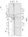
- FIG. 3is a cross-sectional view of the substrate holder shown in FIG. 1 taken along line 3 - 3 .
- FIG. 4is an enlarged cross-sectional view of the substrate holder shown in FIG. 3 that illustrates how an annular compliant member establishes electrical contact between an electrode and a peripheral region of the substrate.
- FIG. 5is an enlarged cross-sectional view of a substrate holder including an electrode having a serrated contact surface for establishing electrical contact with a peripheral region of a substrate according to another embodiment of the invention.
- FIG. 6is an enlarged cross-sectional view of a substrate holder including an electrode having a substantially planar contact surface for establishing electrical contact with a peripheral region of a substrate according to yet another embodiment of the invention.
- FIG. 7is an isometric view of a substrate holder configured to hold two or more substrates according to another embodiment of the invention.
- FIG. 8is plan view of the cover shown in FIG. 7 , with the seals inserted into corresponding seal seats and the electrode inserted into an electrode seat formed in the cover.
- FIG. 9is an enlarged, partial cross-sectional view of the substrate holder shown in FIG. 7 taken along line 9 - 9 .
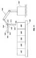
- FIG. 10is schematic diagram of an electroplating system that may utilize any of the disclosed substrate holder embodiments according to another embodiment of the invention.
- FIG. 11is a schematic diagram illustrating how the substrate-holder-transport unit is operable to rotate a substrate holder prior to immersion into a container.
- One or more embodiments of the inventionrelate to a substrate holder configured for holding at least one substrate during electroplating and an electroplating system that may employ such a substrate holder.
- the substrate holdermay be employed in an electroplating system for electroplating a selected surface of the at least one substrate and may further be robust enough to be moved at a selected rate (e.g., in an oscillatory manner and/or rotated) when immersed in the electroplating aqueous solution during electroplating.
- a compliant polymeric materialmay help establish and maintain electrical contact between the at least one substrate and an electrode even when the substrate holder is being moved, and/or may help reduce mechanical play between components of the substrate holder.
- FIGS. 1 , 2 A- 2 B, 3 , and 4show a substrate holder 100 configured to hold at least one substrate according to one embodiment of the invention.
- the substrate holder 100includes a base 102 and a cover 104 , and substrates 106 a and 106 b may be secured therebetween.
- a plurality of fasteners 107may be used to secure the base 102 and cover 104 together to capture the substrates 106 a and 106 b therebetween.
- the base 102 and cover 104may be formed from a material, such as ultra-high molecular weight polypropylene or another suitable material.
- a vacuum mechanismmay be used to attract the base 102 and cover 104 together by way of a vacuum port formed through the base 102 or the cover 104 instead of the fasteners 107 shown in the illustrated embodiment.
- substraterefers to any workpiece capable of being electroplated.
- suitable substratesinclude, but are not limited to, semiconductor substrates (e.g., single-crystal silicon wafers in full or partial form, single-crystal gallium arsenide wafer in full or partial form, etc.) with or without active and/or passive devices (e.g., transistors, diodes, capacitors, resistors, etc.) formed therein and with or without a seed layer formed thereon to promote electroplating, printed circuit boards, flexible polymeric substrates with a conductive film thereon, and many other types of substrates.
- semiconductor substratese.g., single-crystal silicon wafers in full or partial form, single-crystal gallium arsenide wafer in full or partial form, etc.
- active and/or passive devicese.g., transistors, diodes, capacitors, resistors, etc.
- the cover 104includes openings 108 a and 108 b formed therein through which surfaces 110 a and 110 b of corresponding substrates 106 a and 106 b are exposed.
- a bus member 112 of an electrode 206projects out of the assembly of the base 102 and cover 104 to provide an externally accessible feature for electrically connecting the electrode 206 to a voltage source.
- the electrode 206may be made from number of different electrically conductive metals or alloys.
- FIG. 2Ais plan view of the cover 104 shown in FIG. 1 that shows many of the internal components of the substrate holder 100 in more detail.
- the substrate holder 100includes seal assemblies 200 a and 200 b , each of which extends about a corresponding opening 108 a and 108 b of the cover 104 .
- Each seal assembly 200 a and 200 bcomprises an annular, inner seal 202 and an annular, outer seal 204 that extends circumferentially about the inner seal 202 .
- the inner seal 202 and outer seal 204 of each seal assembly 200 a and 200 bmay reside in corresponding seal seats 402 and 404 (See FIG. 4 ) formed in the cover 104 .
- the inner seal 202 and outer seal 204may be an O-ring, a gasket, or another suitable seal.
- the electrode 206 of the substrate holder 100is disposed within an electrode seat 406 (See FIG. 4 ) and under the outer seal 204 .
- the electrode 206includes contact rings 208 a and 208 b (i.e., contact portions), each of which may be generally equally spaced from the bus member 112 and electrically interconnected thereto via interconnects 210 a and 210 b .
- a more uniform current distribution over the surfaces 110 a and 110 b of corresponding substrates 106 a and 106 bmay be obtained during an electroplating process by generally equally spacing the contact rings 208 a and 208 b from the bus member 112 .
- the electrode 206is configured so that the contact ring 208 a may be positioned between the inner seal 202 and outer seal 204 of the seal assembly 200 a and the contact ring 208 b may be positioned between the inner seal 202 and outer seal 204 of the seal assembly 200 b .
- Each interconnect 210 a and 210 bmay include a slot (not shown) formed therein that receives a portion of a corresponding outer seal 204 .
- the contact rings 208 a and 208 bultimately, establish electrical contact with corresponding peripheral regions of the substrates 106 a and 106 b when assembled between the base 102 and the cover 104 .
- the contact rings 208 a and 208 bmay be replaced with partial rings.
- a peripheral seal 211(e.g., an O-ring, a gasket, or the like) may also be provided in a seal seat 408 (See FIG. 4 ) that extends peripherally about the seal assemblies 200 a and 200 b to substantially seal portions of the interconnects 210 a and 210 b and the bus member 112 from the electroplating aqueous solution that the substrate holder 100 is immersed in.
- a plurality of through holes 205may be formed in the cover 104 in which one of the fasteners 107 (See FIG. 1 ) may be inserted therethrough.
- FIG. 2Bmore clearly illustrates the configuration of the base 102 .
- the base 102includes recesses 212 a (not shown) and 212 b in which corresponding substrates 106 a and 106 b (not shown) may be received.
- the recess 212 ais not shown because the substrate 106 a is positioned therein.
- the base 102may further include a plurality of partial or through holes 214 in which one of the fasteners 107 (See FIG. 1 ) may be inserted therein.
- FIGS. 3 and 4best show how the components of the substrate holder 100 assemble together.
- the seal assembly 200 b and contact ring 208 bare not shown in FIGS. 3 and 4 , it should be understood that they function the same as the seal assembly 200 a and contact ring 208 a shown in FIGS. 3 and 4 .
- FIG. 3is a cross-sectional view of the substrate holder 100 shown in FIG. 1 taken along line 3 - 3 and shows the overall assembly of the base 102 , cover 104 , substrate 106 a , and relative positions of the seal assembly 200 a , peripheral seal 211 , and contact ring 208 a.
- FIG. 4is an enlarged cross-sectional view of the substrate holder 100 shown in FIG. 3 that best shows how the contact ring 208 a establishes electrical contact with the substrate 106 a .
- the inner seal 202 and outer seal 204 of the seal assembly 200 aeach resides in corresponding seal seats 402 and 404 , and the contact ring 208 a resides in the electrode seat 406 .
- the seal assembly 200 acomprised of the inner seal 202 and outer seal 204 forms an annular, substantially sealed region 407 adjacent to a peripheral region 410 of the surface 108 a of the substrate 106 a .
- the inner seal 202seals with the peripheral region 410 and the cover 104 , and the outer seal 204 may seal against the base 102 and the cover 104 .
- annular first compliant member 412made from an electrically conductive polymer, is disposed between the contact ring 208 a and peripheral region 410 , and an annular second compliant member 414 made from a polymeric material is disposed between the contact ring 208 a and the cover 104 .
- another first compliant member 412is disposed between the contact ring 208 b and peripheral region 410 .
- the first compliant member 412may contact substantially all of the surface area of the peripheral region 410 so that an electrical potential applied to the substrate 106 a is distributed generally uniformly over the surface 110 a thereof.
- Suitable electrically conductive polymers for the first compliant member 412include, but are not limited to, organic electrically conductive polymers, such as polyacetylene, polypyrrole, polythiophene, polyaniline, polyfluorene, poly(3-alkylthiophene), polytetrathiafulvalene, polynaphthalene, poly(p-phenylene sulfide), and poly(para-phenylene vinylene).
- the first compliant member 412may be made from polyacetylene oxidized with iodine, which exhibits an electrical conductivity similar to that of silver.
- the first compliant member 412may be made from iodine-doped polyacetylene. In another specific embodiment of the invention, the first compliant member 412 may be made from poly(3-dodecylthiophene) doped with iodine. Poly(3-dodecylthiophene) doped with iodine may exhibit an electrical conductivity of about 1000 S/cm. Other organic electrically conductive polymers that the first compliant member 412 may be made from include conductive nylon 8715, polyester urethane 4931, and polyether urethane 4901, each of which is commercially available from HiTech Polymers of Hebron, Ky.
- electrically conductive particlesmay be embedded in a polymeric matrix.
- the first compliant 412may comprise an O-ring (e.g., an O-ring made from Teflon®), polyvinyl fluoride, or polyethylene) partially or completely coated with an electrically conductive film made from a metal or alloy (e.g., gold, copper, or alloys thereof).
- the second compliant 414may be made from the same or similar materials as the first compliant member 412 and does need to be electrically conductive.
- the first compliant member 412establishes electrical contact between the peripheral region 410 of the substrate 106 a and the contact ring 208 a . Because the first compliant member 412 is made from a compliant material (e.g., an electrically conductive polymer), it provides a reliable electrical contact to the peripheral region 410 of the substrate 106 a even when the substrate holder 100 is being moved (e.g., during electroplating).
- the second compliant member 414may help reduce any mechanical play present between the contact ring 208 a and the cover 104 to further help maintain electrical contact between the peripheral region 410 and the first compliant member 412 .
- the stiffness of the first compliant member 412may be less than that of the inner seal 202 and outer seal 204 of the seal assembly 200 b and the peripheral seal 211 so that the sealing force applied to the substrate 106 a is greater than that of the force applied to the contact ring 208 a.
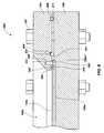
- FIG. 5is an enlarged cross-sectional view of a substrate holder 500 according to another embodiment of the invention.
- the substrate holder 500is structurally similar to the substrate holder 100 shown in FIGS. 1 , 2 A- 2 B, 3 , and 4 . Therefore, in the interest of brevity, components in both substrate holders 100 and 500 that are identical to each other have been provided with the same reference numerals, and an explanation of their structure and function will not be repeated unless the components function differently in the substrate holders 100 and 500 .
- the substrate holder 500differs mainly from the substrate holder 100 shown in FIGS. 1 , 2 A- 2 B, 3 , and 4 in that the substrate holder 500 has a contact ring 208 a ′ with a non-planar contact surface.
- the contact ring 208 a ′includes a serrated contact surface 502 that establishes electrical contact with the peripheral region 410 of the surface 110 a of the substrate 106 a .
- the serrated contact surface 502may help break through any surface oxides or debris present on the surface 110 a of the substrate 106 a.
- FIG. 6is an enlarged cross-sectional view of a substrate holder 600 according to another embodiment of the invention.
- the substrate holder 600is structurally similar to the substrate holder 100 shown in FIGS. 1 , 2 A- 2 B, 3 , and 4 . Therefore, in the interest of brevity, components in both substrate holders 100 and 600 that are identical to each other have been provided with the same reference numerals, and an explanation of their structure and function will not be repeated unless the components function differently in the substrate holders 100 and 600 .
- the substrate holder 600differs mainly from the substrate holder 100 shown in FIGS.
- the substrate holder 600includes a contact ring 208 a ′′ with a substantially planar contact surface 602 that establishes electrical contact with the peripheral region 410 of the surface 110 a of the substrate 110 a.
- the second compliant member 414may be omitted.
- the thickness of the contact rings 208 a / 208 b , 208 a ′, and 208 a ′′should be suitably increased to help prevent any mechanical play with the cover 104 .
- FIG. 7is an isometric view of a substrate holder 700 configured to hold two or more substrates according to another embodiment of the invention.
- the substrate holder 700enables electroplating a greater number of substrates at one time than the substrate holders 100 , 500 , and 600 shown in FIGS. 1 , 5 , and 6 . Accordingly, the substrate holder 700 provides a greater process throughput in electroplating processes than the substrate holders 100 , 500 , and 600 .
- the substrate holder 700includes a base 702 and a cover 704 .
- the cover 704includes a plurality of openings 706 formed therein that expose corresponding surfaces 708 of substrates 710 therethrough captured between the cover 704 and the base 102 .
- a main bus member 802 of an electrode 800projects out of the assembly of the base 102 and cover 104 to provide an externally accessible feature for electrically connecting the electrode 800 to a voltage source during electroplating operations.
- FIG. 8is plan view of the cover 704 shown in FIG. 7 that shows many of the internal components of the substrate holder 700 in more detail. It is noted that the substrate holder 700 differs mainly from the substrate holder 100 in that the structure of the electrode 800 is different. As shown in FIG. 8 , the substrate holder 700 includes a plurality of seal assemblies 804 , each of which includes an inner seal 806 (e.g., an O-ring, a gasket, or the like) and an outer seal 808 (e.g., an O-ring, a gasket, or the like) extending thereabout. Each inner seal 806 and outer seal 808 is disposed in a corresponding seal seat 906 and 908 (See FIG.
- an inner seal 806e.g., an O-ring, a gasket, or the like
- an outer seal 808e.g., an O-ring, a gasket, or the like
- a peripheral seal 810(e.g., an O-ring, a gasket, or the like) similar in structure and functionality to the peripheral seal 211 shown in FIG. 2A of the substrate holder 100 may be disposed in a seal seat 910 (See FIG. 9 ) formed in the cover 704 .
- the electrode 800is disposed within an electrode seat 909 (See FIG. 9 ) formed in the cover 704 and under the outer seals 808 .
- the electrode 800includes bus bars 814 and 816 connected to the main bus member 802 .
- the electrode 800further includes a plurality of contact rings 818 arranged in rows 820 - 822 . Each contact ring 818 of the row 820 is connected to the bus bar 814 via an interconnect 824 , each contact ring 818 of the row 822 is connected to the bus bar 816 via an interconnect 826 , and each contact ring 818 of the row 821 is connected to both the bus bar 814 and 816 via interconnects 828 .
- Each contact ring 818may be spaced from the bus bar 814 , 816 , or both a substantially equal distance.
- FIG. 9is an enlarged, partial cross-sectional view of the substrate holder 700 shown in FIG. 7 taken along line 9 - 9 .
- each contact ring 818is disposed between the inner seal 806 and outer seal 808 of a corresponding seal assembly 804 .
- the seal assemblies 804substantially seal the contact rings 818 from an electroplating aqueous solution that the substrate holder 800 is immersed in.
- vacuum plug 910communicates with the space between the inner seal 806 and outer seal 808 through a vacuum port (not shown) formed in the base 702 so that a vacuum source may be used to attract the base 702 and cover 704 together and engage the seal assemblies 804 and the peripheral seal 810 .
- the vacuum portmay be formed in the base 702 instead of the cover 704 .
- a plurality of fastenersmay be used to urge the base 702 and cover 704 together to engage the seal assemblies 804 and the peripheral seal 810 in a manner similar to the substrate holder 100 shown in FIG. 1 .
- each seal assembly 804forms an annular substantially sealed region 912 adjacent to a peripheral region 914 of the surface 708 of the substrate 710 .
- Each contact ring 818may be disposed within a corresponding sealed region 912 .
- an annular first compliant member 412may be disposed between a corresponding contact ring 818 and the peripheral region 914 to established electrical contact with a corresponding substrate 710 and an annular second compliant member 414 may be disposed between the corresponding contact ring 818 and the cover 704 .
- each contact ring 818 of the electrode 800may have a non-planar contact surface, such as a serrated contact surface similar to the contact ring 208 a ′ shown in FIG. 5 and the first compliant members 414 may be omitted.
- each contact ring 818may have a substantially planar contact surface similar to the contact ring 208 ′′ shown in FIG. 6 and the first compliant members 414 may be omitted.
- the second compliant members 416 used to reduce mechanical play between the electrode 800 and the cover 704may be omitted.
- FIG. 10is a schematic diagram of an electroplating system 1000 that may employ any of the above-described embodiments of substrate holders according to another embodiment of the invention.
- the electroplating system 1000includes a substrate-loading station 1002 that may include a substrate-presentation unit 1004 operable to pick-up a substrate 1006 (a cartridge of substrates 1006 is depicted in FIG. 10 ) and present the substrate 1006 to a substrate-loading unit 1008 .
- the substrate-presentation unit 1004may be a robot with an extensible arm 1010 movable about three axes and having a retention mechanism, such as a vacuum mechanism or forks (as illustrated) that may support the substrate 1006 .
- the substrate-loading unit 1008may include an extensible arm 1012 that is also movable about three axes and may have a similarly configured retention mechanism operable to pick-up and carry one of the substrates 1006 .
- the arm 1012has a range of motion so that it can transport the substrates 1006 to controllably place them onto a base 1014 (depicted configured similar to the base 702 of the substrate holder 700 ).
- the substrate-loading unit 1008may place one of the substrates 1006 in each recess 1016 of the base 1014 .
- the electroplating system 1000further includes a plurality of isolated containers, each of which holds a specific fluid.
- containers 1018 - 1022are shown.
- the container 1018may hold a cleaning solution 1023
- container 1019may hold a rinsing solution 1024 (e.g., water)
- container 1020may hold an electroplating aqueous solution 1025 (e.g., as a sulfuric-acid-based solution)
- container 1021may hold a post-plating cleaning solution 1026
- container 1022may hold a solution (e.g., isopropyl alcohol) to promote drying of a plated substrate after cleaning in the post-plating cleaning solution 1026 .
- the containers 1018 - 1022may be supported on a conveyor 1028 operable to move the containers 1018 - 1022 in conveying directions D 1 and D 2 .
- the electroplating system 1000further includes a substrate-holder transport unit 1030 having an extensible arm 1032 that is movable about three axes.
- the arm 1032may carry a cover 1029 (depicted configured similar to the cover 704 of the substrate holder 700 ) including an electrode (not shown), compliant members (not shown), and various seals (not shown).
- the cover 1029may carry the internal components previously discussed (e.g., the seal assembly, peripheral seal, electrode, compliant members, etc.) with respect to the substrate holders 100 , 500 , and 600 .
- the substrate-holder transport unit 1030may further include provisions for electrically connecting the electrode (not shown) embedded in the cover 1029 to a voltage source 1060 , such as a wire 1034 that extends along the length of the arm 1032 , and a vacuum line 1036 for communicating a vacuum force through one or vacuum ports formed in the cover 1029 .
- a voltage source 1060such as a wire 1034 that extends along the length of the arm 1032
- a vacuum line 1036for communicating a vacuum force through one or vacuum ports formed in the cover 1029 .
- the substrate-holder-transport unit 1030may controllably position the cover 1029 on the base 1014 loaded with substrates 1006 at the substrate-loading station 1002 and communicate a vacuum force through the vacuum line 1036 to urge the base 1014 and cover 1029 together to form an assembled substrate holder 1038 (depicted configured similar to the substrate holder 700 ).
- the substrate-holder-transport unit 1030may rotate the substrate holder 1038 from a generally horizontal orientation to a generally vertical orientation so that the substrate holder 1038 may be more easily immersed in each container 1018 - 1022 .
- the cover 1029 of the substrate holder 1038may be pivotally connected to the arm 1032 via hinge 1031 .
- the substrate holder 1038may be sequentially immersed in each container 1018 - 1022 .
- the substrate holder 1038is moved in the directions D 1 and/or D 2 by extending or retracting the arm 1032 , as desired.
- the containers 1018 - 1022may be translated in the direction D 1 and/or D 2 using the conveyor 1028 , as necessary or desired.
- a selected voltage or voltage waveformmay be applied between the electrode (not shown) embedded in the substrate holder 1038 and an anode 1040 immersed in the electroplating aqueous solution 1025 to cause metals ions from the electroplating aqueous solution to deposit on an exposed surface of the substrates 1006 .
- the substrate-holder-transport unit 1030may move the substrate holder 1038 (e.g., in a linearly oscillatory manner parallel to the anode 1040 in directions T 1 and T 2 ) to help improve electroplating characteristics.
- the substrate-holder-transport unit 1030may be an overhead conveyor system that the cover 1029 is mounted on.
- the electroplating system 1000may also include a substrate-unloading station 1042 having a substrate-unloading unit 1044 that is configured the same or similarly to the substrate-loading unit 1008 .
- the substrate-unloading station 1042may also include a substrate-stacking unit 1046 that is configured the same or similarly to the substrate-loading unit 1008 for carrying substrates 1006 presented to it by the substrate-unloading unit 1044 and stacking the substrates 1006 in a cartridge 1048 .
- the substrate-transport unit 1030may move the substrate holder 1038 including electroplated substrates 1006 carried therein to the substrate-unloading station 1042 and de-activate the vacuum mechanism holding the base 1014 and cover 1029 together to thereby release and leave the base 1014 at the substrate-unloading station 1042 . Then, the substrate-unloading unit 1044 may individually pick-up and present each substrate 1006 to the substrate-stacking unit 1046 for stacking in the cartridge 1048 .
- the electroplating system 1000also comprises a control system 1050 that may include a computer 1052 with a processor 1054 , a memory 1056 , an operator interface 1058 (e.g., a monitor, keyboard, mouse, etc.), and may further include many other familiar computer components.
- the control system 1050may further include a voltage source 1060 operable to apply a selected voltage between the electrode (not shown) embedded in the substrate holder 1038 and the anode 1040 to effect electroplating of the substrates 1006 , and a pump 1062 operable to generate a vacuum force communicated through the vacuum line 1036 that urges the base 1014 and cover 1029 together.
- the control system 1050may be programmed, with computer readable instructions stored on the memory 1056 , to control the operation of the individual components of the electroplating system 1000 (e.g., the substrate-presentation unit 1004 , substrate-loading unit 1008 , substrate-holder-conveyor unit 1030 , substrate-unloading unit 1044 , and substrate-stacking unit 1046 ), as described above.
- the individual components of the electroplating system 1000e.g., the substrate-presentation unit 1004 , substrate-loading unit 1008 , substrate-holder-conveyor unit 1030 , substrate-unloading unit 1044 , and substrate-stacking unit 1046 ), as described above.
Landscapes
- Chemical & Material Sciences (AREA)
- Engineering & Computer Science (AREA)
- Chemical Kinetics & Catalysis (AREA)
- Electrochemistry (AREA)
- Materials Engineering (AREA)
- Metallurgy (AREA)
- Organic Chemistry (AREA)
- Automation & Control Theory (AREA)
- Electroplating Methods And Accessories (AREA)
Abstract
Description
Claims (20)
Priority Applications (1)
| Application Number | Priority Date | Filing Date | Title |
|---|---|---|---|
| US11/906,882US7905994B2 (en) | 2007-10-03 | 2007-10-03 | Substrate holder and electroplating system |
Applications Claiming Priority (1)
| Application Number | Priority Date | Filing Date | Title |
|---|---|---|---|
| US11/906,882US7905994B2 (en) | 2007-10-03 | 2007-10-03 | Substrate holder and electroplating system |
Publications (2)
| Publication Number | Publication Date |
|---|---|
| US20090090631A1 US20090090631A1 (en) | 2009-04-09 |
| US7905994B2true US7905994B2 (en) | 2011-03-15 |
Family
ID=40522340
Family Applications (1)
| Application Number | Title | Priority Date | Filing Date |
|---|---|---|---|
| US11/906,882Active2029-08-02US7905994B2 (en) | 2007-10-03 | 2007-10-03 | Substrate holder and electroplating system |
Country Status (1)
| Country | Link |
|---|---|
| US (1) | US7905994B2 (en) |
Cited By (1)
| Publication number | Priority date | Publication date | Assignee | Title |
|---|---|---|---|---|
| US20160300751A1 (en)* | 2015-04-13 | 2016-10-13 | Suss Microtec Lithography Gmbh | Wafer Treating Device and Sealing Ring for a Wafer Treating Device |
Families Citing this family (3)
| Publication number | Priority date | Publication date | Assignee | Title |
|---|---|---|---|---|
| JP6239417B2 (en) | 2014-03-24 | 2017-11-29 | 株式会社荏原製作所 | Substrate processing equipment |
| JP7242516B2 (en)* | 2019-12-13 | 2023-03-20 | 株式会社荏原製作所 | substrate holder |
| EP3960909B1 (en)* | 2020-08-25 | 2023-11-01 | Semsysco GmbH | Plating frame unit for holding a substrate in a chemical and/or electrolytic surface treatment of the substrate |
Citations (200)
| Publication number | Priority date | Publication date | Assignee | Title |
|---|---|---|---|---|
| US2689808A (en) | 1950-07-29 | 1954-09-21 | Peen Plate Inc | Metal plating |
| US3132043A (en) | 1963-03-25 | 1964-05-05 | Peen Plate Inc | Metal plating |
| US3383293A (en) | 1967-03-03 | 1968-05-14 | Plastic Clad Metal Products In | Processes for drawing and coating metal substrates |
| US3460977A (en) | 1965-02-08 | 1969-08-12 | Minnesota Mining & Mfg | Mechanical plating |
| US3615272A (en) | 1968-11-04 | 1971-10-26 | Dow Corning | Condensed soluble hydrogensilsesquioxane resin |
| US3832291A (en) | 1971-08-20 | 1974-08-27 | M & T Chemicals Inc | Method of preparing surfaces for electroplating |
| US3855085A (en) | 1973-06-14 | 1974-12-17 | Du Pont | Acid zinc electroplating electrolyte, process and additive |
| US3932659A (en) | 1970-07-24 | 1976-01-13 | Beecham Group Limited | Biologically active substance |
| US3998707A (en) | 1975-07-14 | 1976-12-21 | Minnesota Mining And Manufacturing Company | Cadmium electroplating process and bath therefor |
| US4045305A (en) | 1975-07-14 | 1977-08-30 | Minnesota Mining And Manufacturing Company | Cadmium electroplating bath and process |
| US4049510A (en) | 1975-07-07 | 1977-09-20 | Columbia Chemical Corporation | Baths and additives for the electrodeposition of bright zinc |
| US4049505A (en) | 1974-10-14 | 1977-09-20 | Chatterji Arun K | Photoconductors for electrostatic imaging systems |
| US4070256A (en) | 1975-06-16 | 1978-01-24 | Minnesota Mining And Manufacturing Company | Acid zinc electroplating bath and process |
| US4072582A (en) | 1976-12-27 | 1978-02-07 | Columbia Chemical Corporation | Aqueous acid plating bath and additives for producing bright electrodeposits of tin |
| US4075066A (en) | 1977-01-27 | 1978-02-21 | R. O. Hull & Company, Inc. | Electroplating zinc, ammonia-free acid zinc plating bath therefor and additive composition therefor |
| DE2610705C3 (en) | 1976-03-13 | 1978-10-19 | Henkel Kgaa, 4000 Duesseldorf | Acid galvanic copper baths |
| US4134803A (en) | 1977-12-21 | 1979-01-16 | R. O. Hull & Company, Inc. | Nitrogen and sulfur compositions and acid copper plating baths |
| US4139425A (en) | 1978-04-05 | 1979-02-13 | R. O. Hull & Company, Inc. | Composition, plating bath, and method for electroplating tin and/or lead |
| US4146442A (en) | 1978-05-12 | 1979-03-27 | R. O. Hull & Company, Inc. | Zinc electroplating baths and process |
| US4146441A (en) | 1977-10-06 | 1979-03-27 | R. O. Hull & Company, Inc. | Additive compositions, baths, and methods for electrodepositing bright zinc deposits |
| US4162947A (en) | 1978-05-22 | 1979-07-31 | R. O. Hull & Company, Inc. | Acid zinc plating baths and methods for electrodepositing bright zinc deposits |
| US4218292A (en) | 1979-03-22 | 1980-08-19 | Mcgean Chemical Company, Inc. | Bright zinc electroplating bath and method |
| US4285802A (en) | 1980-02-20 | 1981-08-25 | Rynne George B | Zinc-nickel alloy electroplating bath |
| US4336114A (en) | 1981-03-26 | 1982-06-22 | Hooker Chemicals & Plastics Corp. | Electrodeposition of bright copper |
| US4347108A (en) | 1981-05-29 | 1982-08-31 | Rohco, Inc. | Electrodeposition of copper, acidic copper electroplating baths and additives therefor |
| US4374709A (en) | 1980-05-01 | 1983-02-22 | Occidental Chemical Corporation | Process for plating polymeric substrates |
| US4376685A (en) | 1981-06-24 | 1983-03-15 | M&T Chemicals Inc. | Acid copper electroplating baths containing brightening and leveling additives |
| GB2032462B (en) | 1978-09-13 | 1983-05-18 | Kollmorgen Tech Corp | Electroless copper depositon at faster rates |
| US4384930A (en) | 1981-08-21 | 1983-05-24 | Mcgean-Rohco, Inc. | Electroplating baths, additives therefor and methods for the electrodeposition of metals |
| US4388160A (en) | 1980-02-20 | 1983-06-14 | Rynne George B | Zinc-nickel alloy electroplating process |
| US4399266A (en) | 1980-08-26 | 1983-08-16 | Japan Synthetic Rubber Co., Ltd. | Laddery lower alkylpolysilsesquioxane having heat-resistant thin film-formability and process for preparing same |
| US4417957A (en) | 1982-09-03 | 1983-11-29 | Columbia Chemical Corporation | Aqueous acid plating bath and brightener mixture for producing semibright to bright electrodeposits of tin |
| US4512856A (en) | 1979-11-19 | 1985-04-23 | Enthone, Incorporated | Zinc plating solutions and method utilizing ethoxylated/propoxylated polyhydric alcohols |
| US4530741A (en) | 1984-07-12 | 1985-07-23 | Columbia Chemical Corporation | Aqueous acid plating bath and brightener composition for producing bright electrodeposits of tin |
| US4545870A (en) | 1984-08-27 | 1985-10-08 | Columbia Chemical Corporation | Aqueous acid plating bath and brightener composition for producing bright electrodeposits of tin |
| US4582576A (en) | 1985-03-26 | 1986-04-15 | Mcgean-Rohco, Inc. | Plating bath and method for electroplating tin and/or lead |
| US4662999A (en) | 1985-06-26 | 1987-05-05 | Mcgean-Rohco, Inc. | Plating bath and method for electroplating tin and/or lead |
| US4880132A (en) | 1988-07-15 | 1989-11-14 | Mcgean-Rohco, Inc. | Process for plating adherent co-deposit of aluminum, zinc, and tin onto metallic substrates, and apparatus |
| US4885064A (en) | 1989-05-22 | 1989-12-05 | Mcgean-Rohco, Inc. | Additive composition, plating bath and method for electroplating tin and/or lead |
| US4898652A (en) | 1986-03-03 | 1990-02-06 | Omi International Corporation | Polyoxalkylated polyhydroxy compounds as additives in zinc alloy electrolytes |
| US4999397A (en) | 1989-07-28 | 1991-03-12 | Dow Corning Corporation | Metastable silane hydrolyzates and process for their preparation |
| US5051154A (en) | 1988-08-23 | 1991-09-24 | Shipley Company Inc. | Additive for acid-copper electroplating baths to increase throwing power |
| US5174887A (en) | 1987-12-10 | 1992-12-29 | Learonal, Inc. | High speed electroplating of tinplate |
| US5232575A (en) | 1990-07-26 | 1993-08-03 | Mcgean-Rohco, Inc. | Polymeric leveling additive for acid electroplating baths |
| US5252196A (en) | 1991-12-05 | 1993-10-12 | Shipley Company Inc. | Copper electroplating solutions and processes |
| US5282954A (en) | 1991-12-30 | 1994-02-01 | Atotech Usa, Inc. | Alkoxylated diamine surfactants in high-speed tin plating |
| US5328589A (en) | 1992-12-23 | 1994-07-12 | Enthone-Omi, Inc. | Functional fluid additives for acid copper electroplating baths |
| US5415762A (en) | 1993-08-18 | 1995-05-16 | Shipley Company Inc. | Electroplating process and composition |
| US5433840A (en) | 1991-08-07 | 1995-07-18 | Atotech Deutschland Gmbh | Acid bath for the galvanic deposition of copper, and the use of such a bath |
| US5534649A (en) | 1994-10-21 | 1996-07-09 | Tama Chemicals Co., Ltd. | Process for preparing dialkyl carbonates |
| US5575898A (en) | 1994-10-12 | 1996-11-19 | Bayer Ag | Process for through-hole plating of two-layer printed circuit boards and multilayers |
| US5656148A (en) | 1995-03-02 | 1997-08-12 | Atotech Usa, Inc. | High current density zinc chloride electrogalvanizing process and composition |
| US5698087A (en) | 1992-03-11 | 1997-12-16 | Mcgean-Rohco, Inc. | Plating bath and method for electroplating tin and/or lead |
| US5833820A (en) | 1997-06-19 | 1998-11-10 | Advanced Micro Devices, Inc. | Electroplating apparatus |
| US5882498A (en) | 1997-10-16 | 1999-03-16 | Advanced Micro Devices, Inc. | Method for reducing oxidation of electroplating chamber contacts and improving uniform electroplating of a substrate |
| US5965679A (en) | 1996-09-10 | 1999-10-12 | The Dow Chemical Company | Polyphenylene oligomers and polymers |
| US5972192A (en) | 1997-07-23 | 1999-10-26 | Advanced Micro Devices, Inc. | Pulse electroplating copper or copper alloys |
| US6024857A (en) | 1997-10-08 | 2000-02-15 | Novellus Systems, Inc. | Electroplating additive for filling sub-micron features |
| US6024856A (en) | 1997-10-10 | 2000-02-15 | Enthone-Omi, Inc. | Copper metallization of silicon wafers using insoluble anodes |
| US6077405A (en) | 1998-10-28 | 2000-06-20 | International Business Machines Corporation | Method and apparatus for making electrical contact to a substrate during electroplating |
| US6083838A (en) | 1998-05-20 | 2000-07-04 | Lucent Technologies Inc. | Method of planarizing a surface on a semiconductor wafer |
| US6093636A (en) | 1998-07-08 | 2000-07-25 | International Business Machines Corporation | Process for manufacture of integrated circuit device using a matrix comprising porous high temperature thermosets |
| US6107357A (en) | 1999-11-16 | 2000-08-22 | International Business Machines Corporatrion | Dielectric compositions and method for their manufacture |
| US6113771A (en) | 1998-04-21 | 2000-09-05 | Applied Materials, Inc. | Electro deposition chemistry |
| US6129830A (en) | 1996-12-13 | 2000-10-10 | Atotech Deutschland Gmbh | Process for the electrolytic deposition of copper layers |
| US6193789B1 (en) | 1996-06-03 | 2001-02-27 | Hideo Honma | Electroless copper plating solution and method for electroless copper plating |
| US6204202B1 (en) | 1999-04-14 | 2001-03-20 | Alliedsignal, Inc. | Low dielectric constant porous films |
| US6231989B1 (en) | 1998-11-20 | 2001-05-15 | Dow Corning Corporation | Method of forming coatings |
| US6251710B1 (en) | 2000-04-27 | 2001-06-26 | International Business Machines Corporation | Method of making a dual damascene anti-fuse with via before wire |
| US6258241B1 (en) | 1997-12-10 | 2001-07-10 | Lucent Technologies, Inc. | Process for electroplating metals |
| US6277450B1 (en) | 1998-01-26 | 2001-08-21 | Mohammad W. Katoot | Method and composition for preventing corrosion |
| US20010015321A1 (en) | 1998-10-26 | 2001-08-23 | Reid Jonathan D. | Electroplating process for avoiding defects in metal features of integrated circuit devices |
| US20010047943A1 (en) | 1999-05-17 | 2001-12-06 | Leon Barstad | Electrolytic copper plating solutions |
| US20020000382A1 (en) | 1999-12-15 | 2002-01-03 | Shipley Company, L.L.C. Of Marlborough | Seed layer repair method |
| US6338411B1 (en) | 1998-12-02 | 2002-01-15 | Katabe Toyokazu | Screw drum type filtration device |
| US6344413B1 (en) | 1997-12-22 | 2002-02-05 | Motorola Inc. | Method for forming a semiconductor device |
| US6344129B1 (en) | 1999-10-13 | 2002-02-05 | International Business Machines Corporation | Method for plating copper conductors and devices formed |
| US6350386B1 (en) | 2000-09-20 | 2002-02-26 | Charles W. C. Lin | Method of making a support circuit with a tapered through-hole for a semiconductor chip assembly |
| US6352467B1 (en) | 1997-11-10 | 2002-03-05 | Applied Materials, Inc. | Integrated electrodeposition and chemical mechanical polishing tool |
| US6358388B1 (en) | 1996-07-15 | 2002-03-19 | Semitool, Inc. | Plating system workpiece support having workpiece-engaging electrodes with distal contact-part and dielectric cover |
| US6358832B1 (en) | 1999-09-30 | 2002-03-19 | International Business Machines Corporation | Method of forming barrier layers for damascene interconnects |
| US6362099B1 (en) | 1999-03-09 | 2002-03-26 | Applied Materials, Inc. | Method for enhancing the adhesion of copper deposited by chemical vapor deposition |
| US6368484B1 (en) | 2000-05-09 | 2002-04-09 | International Business Machines Corporation | Selective plating process |
| US6368966B1 (en) | 1998-06-30 | 2002-04-09 | Semitool, Inc. | Metallization structures for microelectronic applications and process for forming the structures |
| US20020043468A1 (en) | 2000-10-13 | 2002-04-18 | Shipley Company, L.L.C. | Seed repair and electroplating bath |
| US20020043467A1 (en) | 2000-10-13 | 2002-04-18 | Shipley Company, L.L.C. | Electrolyte |
| US6379745B1 (en) | 1997-02-20 | 2002-04-30 | Parelec, Inc. | Low temperature method and compositions for producing electrical conductors |
| US6380083B1 (en) | 1998-08-28 | 2002-04-30 | Agere Systems Guardian Corp. | Process for semiconductor device fabrication having copper interconnects |
| US6379522B1 (en) | 1999-01-11 | 2002-04-30 | Applied Materials, Inc. | Electrodeposition chemistry for filling of apertures with reflective metal |
| US20020053519A1 (en) | 2000-11-02 | 2002-05-09 | Shipley Company, L.L.C. | Seed layer repair |
| US6395199B1 (en) | 2000-06-07 | 2002-05-28 | Graftech Inc. | Process for providing increased conductivity to a material |
| US6403481B1 (en) | 1998-08-11 | 2002-06-11 | Kabushiki Kaisha Toshiba | Film formation method |
| US6406794B1 (en) | 2001-02-08 | 2002-06-18 | Jsr Corporation | Film-forming composition |
| US20020074242A1 (en) | 2000-10-13 | 2002-06-20 | Shipley Company, L.L.C. | Seed layer recovery |
| US20020074231A1 (en) | 2000-10-13 | 2002-06-20 | Shipley Company, L.L.C. | Electroplating method |
| US6413882B1 (en) | 1999-04-14 | 2002-07-02 | Alliedsignal Inc. | Low dielectric foam dielectric formed from polymer decomposition |
| US20020084193A1 (en) | 2000-10-25 | 2002-07-04 | Shipley Company, L.L.C. | Seed layer |
| US20020090484A1 (en) | 2000-10-20 | 2002-07-11 | Shipley Company, L.L.C. | Plating bath |
| US20020088713A1 (en) | 2000-10-20 | 2002-07-11 | Shipley Company, L.L.C. | Seed layer repair bath |
| US6423770B1 (en) | 1999-07-15 | 2002-07-23 | Lucent Technologies Inc. | Silicate material and process for fabricating silicate material |
| US6425996B1 (en) | 1997-12-17 | 2002-07-30 | Atotech Deutschland Gmbh | Water bath and method for electrolytic deposition of copper coatings |
| US6432821B1 (en) | 2000-12-18 | 2002-08-13 | Intel Corporation | Method of copper electroplating |
| US20020112964A1 (en) | 2000-07-12 | 2002-08-22 | Applied Materials, Inc. | Process window for gap-fill on very high aspect ratio structures using additives in low acid copper baths |
| JP2002248397A (en) | 2001-02-26 | 2002-09-03 | Konica Corp | Slide type coater for simultaneous multiple coating and method for manufacturing recording material using the same |
| US20020127847A1 (en) | 2000-11-03 | 2002-09-12 | Shipley Company, L.L.C. | Electrochemical co-deposition of metals for electronic device manufacture |
| US20020134684A1 (en) | 2000-10-25 | 2002-09-26 | Shipley Company, L.L.C. | Seed layer processes |
| US6465606B2 (en) | 1993-07-13 | 2002-10-15 | Huntsman Petrochemical Corporation | Polyether monoamine with 36-44 EO units and 1-6 PO units |
| US20020153260A1 (en) | 2000-07-01 | 2002-10-24 | Shipley Company, L.L.C. | Metal alloy compositions and plating methods related thereto |
| US6491806B1 (en) | 2000-04-27 | 2002-12-10 | Intel Corporation | Electroplating bath composition |
| US6511912B1 (en) | 2000-08-22 | 2003-01-28 | Micron Technology, Inc. | Method of forming a non-conformal layer over and exposing a trench |
| US6518182B1 (en) | 1999-11-12 | 2003-02-11 | Ebara-Udylite Co., Ltd. | Via-filling process |
| US6544399B1 (en) | 1999-01-11 | 2003-04-08 | Applied Materials, Inc. | Electrodeposition chemistry for filling apertures with reflective metal |
| US6551487B1 (en) | 2001-05-31 | 2003-04-22 | Novellus Systems, Inc. | Methods and apparatus for controlled-angle wafer immersion |
| US6562555B2 (en) | 2001-08-01 | 2003-05-13 | Kodak Polychrome Graphics Llc | Method for developing lithographic printing plate precursors using a coating attack-suppressing agent |
| US20030094376A1 (en) | 2000-12-20 | 2003-05-22 | Shipley Company, L.L.C. | Electrolytic copper plating solution and method for controlling the same |
| US6569302B1 (en)* | 1998-12-22 | 2003-05-27 | Steag Micro Tech Gmbh | Substrate carrier |
| US20030106802A1 (en) | 2001-05-09 | 2003-06-12 | Hideki Hagiwara | Copper plating bath and plating method for substrate using the copper plating bath |
| US6605204B1 (en) | 1999-10-14 | 2003-08-12 | Atofina Chemicals, Inc. | Electroplating of copper from alkanesulfonate electrolytes |
| US6607654B2 (en) | 2000-09-27 | 2003-08-19 | Samsung Electronics Co., Ltd. | Copper-plating elecrolyte containing polyvinylpyrrolidone and method for forming a copper interconnect |
| US6610192B1 (en) | 2000-11-02 | 2003-08-26 | Shipley Company, L.L.C. | Copper electroplating |
| US20030168343A1 (en) | 2002-03-05 | 2003-09-11 | John Commander | Defect reduction in electrodeposited copper for semiconductor applications |
| US20030205476A1 (en) | 2000-10-20 | 2003-11-06 | Shipley Company, L.L.C. | Electroplating bath control |
| US6676823B1 (en) | 2002-03-18 | 2004-01-13 | Taskem, Inc. | High speed acid copper plating |
| US6685817B1 (en) | 1995-05-26 | 2004-02-03 | Formfactor, Inc. | Method and apparatus for controlling plating over a face of a substrate |
| US6709562B1 (en) | 1995-12-29 | 2004-03-23 | International Business Machines Corporation | Method of making electroplated interconnection structures on integrated circuit chips |
| US6709564B1 (en) | 1999-09-30 | 2004-03-23 | Rockwell Scientific Licensing, Llc | Integrated circuit plating using highly-complexed copper plating baths |
| US20040074775A1 (en) | 2002-10-21 | 2004-04-22 | Herdman Roderick Dennis | Pulse reverse electrolysis of acidic copper electroplating solutions |
| US6740221B2 (en) | 2001-03-15 | 2004-05-25 | Applied Materials Inc. | Method of forming copper interconnects |
| EP1422320A1 (en) | 2002-11-21 | 2004-05-26 | Shipley Company, L.L.C. | Copper electroplating bath |
| US6743211B1 (en) | 1999-11-23 | 2004-06-01 | Georgia Tech Research Corporation | Devices and methods for enhanced microneedle penetration of biological barriers |
| US6746589B2 (en) | 2000-09-20 | 2004-06-08 | Ebara Corporation | Plating method and plating apparatus |
| US20040127009A1 (en) | 2002-12-25 | 2004-07-01 | Advanced Semiconductor Engineering, Inc. | Bumping process |
| US20040138075A1 (en) | 2002-11-01 | 2004-07-15 | Brown David W. | Coatings for metal containers, metalworking lubricant compositions, compositions for electroplating and electrowinning, latex compositions and processes therefor |
| US6774051B2 (en) | 2002-06-12 | 2004-08-10 | Macronix International Co., Ltd. | Method for reducing pitch |
| US20040154926A1 (en) | 2002-12-24 | 2004-08-12 | Zhi-Wen Sun | Multiple chemistry electrochemical plating method |
| US6776893B1 (en) | 2000-11-20 | 2004-08-17 | Enthone Inc. | Electroplating chemistry for the CU filling of submicron features of VLSI/ULSI interconnect |
| US20040168928A1 (en) | 2003-02-27 | 2004-09-02 | Vishwas Hardikar | Composition and method for electrodeposition of metal on a work piece |
| US6797142B2 (en) | 2001-05-24 | 2004-09-28 | Shipley Company, L.L.C. | Tin plating |
| US20040222104A1 (en) | 2003-02-19 | 2004-11-11 | Rohm And Haas Electronic Materials, L.L.C | Electroplating composition |
| US20040249177A1 (en) | 2003-06-04 | 2004-12-09 | Shipley Company, L.L.C. | Leveler compounds |
| US6835294B2 (en) | 2001-06-07 | 2004-12-28 | Shipley Company, L.L.C. | Electrolytic copper plating method |
| US20050006245A1 (en) | 2003-07-08 | 2005-01-13 | Applied Materials, Inc. | Multiple-step electrodeposition process for direct copper plating on barrier metals |
| US6844274B2 (en)* | 2002-08-13 | 2005-01-18 | Ebara Corporation | Substrate holder, plating apparatus, and plating method |
| US20050014368A1 (en) | 2002-06-21 | 2005-01-20 | Junichiro Yoshioka | Substrate holder and plating apparatus |
| US20050020068A1 (en) | 2003-05-23 | 2005-01-27 | Rohm And Haas Electronic Materials, L.L.C. | Plating method |
| US20050016858A1 (en) | 2002-12-20 | 2005-01-27 | Shipley Company, L.L.C. | Reverse pulse plating composition and method |
| US20050025960A1 (en) | 2003-06-24 | 2005-02-03 | Rohm And Haas Electronic Materials, L.L.C. | Catalyst composition and deposition method |
| US20050045488A1 (en) | 2002-03-05 | 2005-03-03 | Enthone Inc. | Copper electrodeposition in microelectronics |
| US20050045485A1 (en) | 2003-09-03 | 2005-03-03 | Taiwan Semiconductor Manufacturing Co. Ltd. | Method to improve copper electrochemical deposition |
| US20050061679A1 (en) | 2003-09-18 | 2005-03-24 | Hardikar Vishwas V. | Methods for depositing copper on a noble metal layer of a work piece |
| US20050067297A1 (en) | 2003-09-26 | 2005-03-31 | Innovative Technology Licensing, Llc | Copper bath for electroplating fine circuitry on semiconductor chips |
| US20050077180A1 (en) | 2003-10-08 | 2005-04-14 | Zierath Daniel J. | Modified electroplating solution components in a high-acid electrolyte solution |
| US20050081744A1 (en) | 2003-10-16 | 2005-04-21 | Semitool, Inc. | Electroplating compositions and methods for electroplating |
| US20050133376A1 (en) | 2003-12-19 | 2005-06-23 | Opaskar Vincent C. | Alkaline zinc-nickel alloy plating compositions, processes and articles therefrom |
| US6924224B2 (en) | 2002-10-03 | 2005-08-02 | International Business Machines Corporation | Method of forming filled blind vias |
| US6926922B2 (en) | 2002-04-09 | 2005-08-09 | Shipley Company, L.L.C. | PWB manufacture |
| US20050176604A1 (en) | 2004-02-10 | 2005-08-11 | Kwang-Wook Lee | Corrosion-inhibiting cleaning compositions for metal layers and patterns on semiconductor substrates |
| US20050189233A1 (en) | 2004-02-27 | 2005-09-01 | Taiwan Semiconductor Manufacturing Co., Ltd. | ECP polymer additives and method for reducing overburden and defects |
| US20050199507A1 (en) | 2004-03-09 | 2005-09-15 | Taiwan Semiconductor Manufacturing Co., Ltd. | Chemical structures and compositions of ECP additives to reduce pit defects |
| US6946716B2 (en) | 1995-12-29 | 2005-09-20 | International Business Machines Corporation | Electroplated interconnection structures on integrated circuit chips |
| US20050211564A1 (en) | 2004-03-29 | 2005-09-29 | Taiwan Semiconductor Manufacturing Co., Ltd. | Method and composition to enhance wetting of ECP electrolyte to copper seed |
| US20050230354A1 (en) | 2004-04-14 | 2005-10-20 | Hardikar Vishwas V | Method and composition of post-CMP wetting of thin films |
| US20050230263A1 (en) | 2002-12-05 | 2005-10-20 | Dubin Valery M | Methods for forming interconnect structures by co-plating of noble metals and structures formed thereby |
| US20050241946A1 (en) | 2003-12-25 | 2005-11-03 | Mizuki Nagai | Plating apparatus and plating method |
| US20050274620A1 (en) | 2004-06-15 | 2005-12-15 | Kovarsky Nicolay Y | Copper replenishment system for interconnect applications |
| US20050274622A1 (en) | 2004-06-10 | 2005-12-15 | Zhi-Wen Sun | Plating chemistry and method of single-step electroplating of copper on a barrier metal |
| US20050287818A1 (en) | 2004-06-21 | 2005-12-29 | Nat Inst Of Adv Industrial Sci And Tech | Material and method for forming low-dielectric-constant film |
| US20060003566A1 (en) | 2004-06-30 | 2006-01-05 | Ismail Emesh | Methods and apparatuses for semiconductor fabrication utilizing through-wafer interconnects |
| US20060024430A1 (en) | 2004-07-29 | 2006-02-02 | Enthone Inc. | Silver plating in electronics manufacture |
| US20060046079A1 (en) | 2004-09-01 | 2006-03-02 | Samsung Corning Co., Ltd. | Method for preparing surfactant-templated, mesoporous low dielectric film |
| EP1489201A3 (en) | 2003-06-18 | 2006-05-17 | Raschig GmbH | Propanesulfonated or 2-hydroxy-propanesulfonated alkylamine alkoxylates, their preparation and use as additives for the electrolytic deposition of metallic layers |
| US20060118422A1 (en) | 2004-12-03 | 2006-06-08 | Taiwan Semiconductor Manufacturing Co., Ltd. | Electro chemical plating addictives for improving stress and leveling effect |
| US20060141156A1 (en) | 2003-02-17 | 2006-06-29 | Commissariat A L'energie Atomique | Surface-coating method |
| US20060141784A1 (en) | 2004-11-12 | 2006-06-29 | Enthone Inc. | Copper electrodeposition in microelectronics |
| US20060183328A1 (en) | 1999-05-17 | 2006-08-17 | Barstad Leon R | Electrolytic copper plating solutions |
| US20060213780A1 (en) | 2005-03-24 | 2006-09-28 | Taiwan Semiconductor Manufacturing Co., Ltd. | Electroplating composition and method |
| US20060225605A1 (en) | 2005-04-11 | 2006-10-12 | Kloeckener James R | Aqueous coating compositions and process for treating metal plated substrates |
| US7179736B2 (en) | 2004-10-14 | 2007-02-20 | Lsi Logic Corporation | Method for fabricating planar semiconductor wafers |
| US7204865B2 (en) | 2003-09-05 | 2007-04-17 | Fujimi Incorporated | Polishing composition |
| US20080009132A1 (en) | 2006-06-27 | 2008-01-10 | Disco Corporation | Via hole forming method |
| US20080009136A1 (en) | 2004-07-15 | 2008-01-10 | Samsung Electronics Co., Ltd., | Polishing Method |
| US7338689B2 (en) | 2005-02-07 | 2008-03-04 | Samsung Electronics Co., Ltd. | Composition for forming low dielectric thin film including siloxane monomer or siloxane polymer having only one type of stereoisomer and method of producing low dielectric thin film using same |
| US7344986B2 (en) | 2001-11-06 | 2008-03-18 | Ebara Corporation | Plating solution, semiconductor device and method for manufacturing the same |
| US20080090333A1 (en) | 2006-10-17 | 2008-04-17 | Tessera, Inc. | Microelectronic packages fabricated at the wafer level and methods therefor |
| US20080087549A1 (en) | 2004-08-18 | 2008-04-17 | Ebara-Udylite Co.,Ltd. | Additive For Copper Plating And Process For Producing Electronic Circiut Substrate Therewith |
| US7368045B2 (en) | 2005-01-27 | 2008-05-06 | International Business Machines Corporation | Gate stack engineering by electrochemical processing utilizing through-gate-dielectric current flow |
| US7371311B2 (en) | 2003-10-08 | 2008-05-13 | Intel Corporation | Modified electroplating solution components in a low-acid electrolyte solution |
| US7405163B1 (en) | 2003-12-17 | 2008-07-29 | Novellus Systems, Inc. | Selectively accelerated plating of metal features |
| US7413976B2 (en) | 2005-02-01 | 2008-08-19 | Taiwan Semiconductor Manufacturing Company, Ltd. | Uniform passivation method for conductive features |
| US20080221004A1 (en) | 2005-05-25 | 2008-09-11 | Freescale Semiconductor, Inc. | Cleaning Solution for a Semiconductor Wafer |
| US20080230393A1 (en) | 2007-03-23 | 2008-09-25 | Fujifilm Corporation | Method and apparatus for producing conductive material |
| US7429401B2 (en) | 2003-05-23 | 2008-09-30 | The United States of America as represented by the Secretary of Commerce, the National Insitiute of Standards & Technology | Superconformal metal deposition using derivatized substrates |
| US7439182B2 (en) | 2005-07-11 | 2008-10-21 | Dongbu Electronics Co., Ltd. | Semiconductor device and method of fabricating the same |
| US7442267B1 (en) | 2004-11-29 | 2008-10-28 | Novellus Systems, Inc. | Anneal of ruthenium seed layer to improve copper plating |
| US7449098B1 (en) | 1999-10-05 | 2008-11-11 | Novellus Systems, Inc. | Method for planar electroplating |
| US20090023820A1 (en) | 2006-02-22 | 2009-01-22 | Basf Se | Surfactant mixture containing short-chain and also long-chain components |
| US7524347B2 (en) | 2004-10-28 | 2009-04-28 | Cabot Microelectronics Corporation | CMP composition comprising surfactant |
| US20090170306A1 (en) | 2006-03-30 | 2009-07-02 | Freescale Semicondutor Inc | Process for filling recessed features in a dielectric substrate |
| US7575666B2 (en) | 2006-04-05 | 2009-08-18 | James Watkowski | Process for electrolytically plating copper |
| US7598168B2 (en) | 2004-02-06 | 2009-10-06 | Samsung Electronics Co., Ltd. | Method of fabricating dual damascene interconnection and etchant for stripping sacrificial layer |
Family Cites Families (3)
| Publication number | Priority date | Publication date | Assignee | Title |
|---|---|---|---|---|
| US20050023149A1 (en)* | 2003-06-05 | 2005-02-03 | Tsutomu Nakada | Plating apparatus, plating method and substrate processing apparatus |
| JP2008098449A (en)* | 2006-10-12 | 2008-04-24 | Ebara Corp | Substrate processing apparatus and substrate processing method |
| US20090095634A1 (en)* | 2007-10-15 | 2009-04-16 | Natsuki Makino | Plating method |
- 2007
- 2007-10-03USUS11/906,882patent/US7905994B2/enactiveActive
Patent Citations (233)
| Publication number | Priority date | Publication date | Assignee | Title |
|---|---|---|---|---|
| US2689808A (en) | 1950-07-29 | 1954-09-21 | Peen Plate Inc | Metal plating |
| US3132043A (en) | 1963-03-25 | 1964-05-05 | Peen Plate Inc | Metal plating |
| US3460977A (en) | 1965-02-08 | 1969-08-12 | Minnesota Mining & Mfg | Mechanical plating |
| US3383293A (en) | 1967-03-03 | 1968-05-14 | Plastic Clad Metal Products In | Processes for drawing and coating metal substrates |
| US3615272A (en) | 1968-11-04 | 1971-10-26 | Dow Corning | Condensed soluble hydrogensilsesquioxane resin |
| US3932659A (en) | 1970-07-24 | 1976-01-13 | Beecham Group Limited | Biologically active substance |
| US3832291A (en) | 1971-08-20 | 1974-08-27 | M & T Chemicals Inc | Method of preparing surfaces for electroplating |
| US3855085A (en) | 1973-06-14 | 1974-12-17 | Du Pont | Acid zinc electroplating electrolyte, process and additive |
| US4049505A (en) | 1974-10-14 | 1977-09-20 | Chatterji Arun K | Photoconductors for electrostatic imaging systems |
| US4070256A (en) | 1975-06-16 | 1978-01-24 | Minnesota Mining And Manufacturing Company | Acid zinc electroplating bath and process |
| US4070256B1 (en) | 1975-06-16 | 1983-03-01 | ||
| US4049510A (en) | 1975-07-07 | 1977-09-20 | Columbia Chemical Corporation | Baths and additives for the electrodeposition of bright zinc |
| US3998707A (en) | 1975-07-14 | 1976-12-21 | Minnesota Mining And Manufacturing Company | Cadmium electroplating process and bath therefor |
| US4045305A (en) | 1975-07-14 | 1977-08-30 | Minnesota Mining And Manufacturing Company | Cadmium electroplating bath and process |
| DE2610705C3 (en) | 1976-03-13 | 1978-10-19 | Henkel Kgaa, 4000 Duesseldorf | Acid galvanic copper baths |
| US4072582A (en) | 1976-12-27 | 1978-02-07 | Columbia Chemical Corporation | Aqueous acid plating bath and additives for producing bright electrodeposits of tin |
| US4075066A (en) | 1977-01-27 | 1978-02-21 | R. O. Hull & Company, Inc. | Electroplating zinc, ammonia-free acid zinc plating bath therefor and additive composition therefor |
| US4146441A (en) | 1977-10-06 | 1979-03-27 | R. O. Hull & Company, Inc. | Additive compositions, baths, and methods for electrodepositing bright zinc deposits |
| US4134803A (en) | 1977-12-21 | 1979-01-16 | R. O. Hull & Company, Inc. | Nitrogen and sulfur compositions and acid copper plating baths |
| US4139425A (en) | 1978-04-05 | 1979-02-13 | R. O. Hull & Company, Inc. | Composition, plating bath, and method for electroplating tin and/or lead |
| US4146442A (en) | 1978-05-12 | 1979-03-27 | R. O. Hull & Company, Inc. | Zinc electroplating baths and process |
| US4162947A (en) | 1978-05-22 | 1979-07-31 | R. O. Hull & Company, Inc. | Acid zinc plating baths and methods for electrodepositing bright zinc deposits |
| GB2032462B (en) | 1978-09-13 | 1983-05-18 | Kollmorgen Tech Corp | Electroless copper depositon at faster rates |
| US4218292A (en) | 1979-03-22 | 1980-08-19 | Mcgean Chemical Company, Inc. | Bright zinc electroplating bath and method |
| US4512856A (en) | 1979-11-19 | 1985-04-23 | Enthone, Incorporated | Zinc plating solutions and method utilizing ethoxylated/propoxylated polyhydric alcohols |
| US4285802A (en) | 1980-02-20 | 1981-08-25 | Rynne George B | Zinc-nickel alloy electroplating bath |
| US4388160A (en) | 1980-02-20 | 1983-06-14 | Rynne George B | Zinc-nickel alloy electroplating process |
| US4374709A (en) | 1980-05-01 | 1983-02-22 | Occidental Chemical Corporation | Process for plating polymeric substrates |
| US4399266A (en) | 1980-08-26 | 1983-08-16 | Japan Synthetic Rubber Co., Ltd. | Laddery lower alkylpolysilsesquioxane having heat-resistant thin film-formability and process for preparing same |
| US4336114A (en) | 1981-03-26 | 1982-06-22 | Hooker Chemicals & Plastics Corp. | Electrodeposition of bright copper |
| US4347108A (en) | 1981-05-29 | 1982-08-31 | Rohco, Inc. | Electrodeposition of copper, acidic copper electroplating baths and additives therefor |
| US4376685A (en) | 1981-06-24 | 1983-03-15 | M&T Chemicals Inc. | Acid copper electroplating baths containing brightening and leveling additives |
| US4384930A (en) | 1981-08-21 | 1983-05-24 | Mcgean-Rohco, Inc. | Electroplating baths, additives therefor and methods for the electrodeposition of metals |
| US4417957A (en) | 1982-09-03 | 1983-11-29 | Columbia Chemical Corporation | Aqueous acid plating bath and brightener mixture for producing semibright to bright electrodeposits of tin |
| US4530741A (en) | 1984-07-12 | 1985-07-23 | Columbia Chemical Corporation | Aqueous acid plating bath and brightener composition for producing bright electrodeposits of tin |
| US4545870A (en) | 1984-08-27 | 1985-10-08 | Columbia Chemical Corporation | Aqueous acid plating bath and brightener composition for producing bright electrodeposits of tin |
| US4582576A (en) | 1985-03-26 | 1986-04-15 | Mcgean-Rohco, Inc. | Plating bath and method for electroplating tin and/or lead |
| US4662999A (en) | 1985-06-26 | 1987-05-05 | Mcgean-Rohco, Inc. | Plating bath and method for electroplating tin and/or lead |
| US4898652A (en) | 1986-03-03 | 1990-02-06 | Omi International Corporation | Polyoxalkylated polyhydroxy compounds as additives in zinc alloy electrolytes |
| US5174887A (en) | 1987-12-10 | 1992-12-29 | Learonal, Inc. | High speed electroplating of tinplate |
| US4880132A (en) | 1988-07-15 | 1989-11-14 | Mcgean-Rohco, Inc. | Process for plating adherent co-deposit of aluminum, zinc, and tin onto metallic substrates, and apparatus |
| US5051154A (en) | 1988-08-23 | 1991-09-24 | Shipley Company Inc. | Additive for acid-copper electroplating baths to increase throwing power |
| US4885064A (en) | 1989-05-22 | 1989-12-05 | Mcgean-Rohco, Inc. | Additive composition, plating bath and method for electroplating tin and/or lead |
| US4999397A (en) | 1989-07-28 | 1991-03-12 | Dow Corning Corporation | Metastable silane hydrolyzates and process for their preparation |
| US5232575A (en) | 1990-07-26 | 1993-08-03 | Mcgean-Rohco, Inc. | Polymeric leveling additive for acid electroplating baths |
| US5433840A (en) | 1991-08-07 | 1995-07-18 | Atotech Deutschland Gmbh | Acid bath for the galvanic deposition of copper, and the use of such a bath |
| US5252196A (en) | 1991-12-05 | 1993-10-12 | Shipley Company Inc. | Copper electroplating solutions and processes |
| US5282954A (en) | 1991-12-30 | 1994-02-01 | Atotech Usa, Inc. | Alkoxylated diamine surfactants in high-speed tin plating |
| US5698087A (en) | 1992-03-11 | 1997-12-16 | Mcgean-Rohco, Inc. | Plating bath and method for electroplating tin and/or lead |
| US5328589A (en) | 1992-12-23 | 1994-07-12 | Enthone-Omi, Inc. | Functional fluid additives for acid copper electroplating baths |
| US6465606B2 (en) | 1993-07-13 | 2002-10-15 | Huntsman Petrochemical Corporation | Polyether monoamine with 36-44 EO units and 1-6 PO units |
| US5415762A (en) | 1993-08-18 | 1995-05-16 | Shipley Company Inc. | Electroplating process and composition |
| US5528000A (en) | 1993-08-18 | 1996-06-18 | Shipley Company, L.L.C. | Electroplating process and composition |
| US5575898A (en) | 1994-10-12 | 1996-11-19 | Bayer Ag | Process for through-hole plating of two-layer printed circuit boards and multilayers |
| US5534649A (en) | 1994-10-21 | 1996-07-09 | Tama Chemicals Co., Ltd. | Process for preparing dialkyl carbonates |
| US5656148A (en) | 1995-03-02 | 1997-08-12 | Atotech Usa, Inc. | High current density zinc chloride electrogalvanizing process and composition |
| US6685817B1 (en) | 1995-05-26 | 2004-02-03 | Formfactor, Inc. | Method and apparatus for controlling plating over a face of a substrate |
| US6946716B2 (en) | 1995-12-29 | 2005-09-20 | International Business Machines Corporation | Electroplated interconnection structures on integrated circuit chips |
| US6709562B1 (en) | 1995-12-29 | 2004-03-23 | International Business Machines Corporation | Method of making electroplated interconnection structures on integrated circuit chips |
| US6193789B1 (en) | 1996-06-03 | 2001-02-27 | Hideo Honma | Electroless copper plating solution and method for electroless copper plating |
| US6358388B1 (en) | 1996-07-15 | 2002-03-19 | Semitool, Inc. | Plating system workpiece support having workpiece-engaging electrodes with distal contact-part and dielectric cover |
| US5965679A (en) | 1996-09-10 | 1999-10-12 | The Dow Chemical Company | Polyphenylene oligomers and polymers |
| US6129830A (en) | 1996-12-13 | 2000-10-10 | Atotech Deutschland Gmbh | Process for the electrolytic deposition of copper layers |
| US6379745B1 (en) | 1997-02-20 | 2002-04-30 | Parelec, Inc. | Low temperature method and compositions for producing electrical conductors |
| US5833820A (en) | 1997-06-19 | 1998-11-10 | Advanced Micro Devices, Inc. | Electroplating apparatus |
| US5972192A (en) | 1997-07-23 | 1999-10-26 | Advanced Micro Devices, Inc. | Pulse electroplating copper or copper alloys |
| US6024857A (en) | 1997-10-08 | 2000-02-15 | Novellus Systems, Inc. | Electroplating additive for filling sub-micron features |
| US6284121B1 (en) | 1997-10-08 | 2001-09-04 | Novellus Systems, Inc. | Electroplating system including additive for filling sub-micron features |
| US6024856A (en) | 1997-10-10 | 2000-02-15 | Enthone-Omi, Inc. | Copper metallization of silicon wafers using insoluble anodes |
| US5882498A (en) | 1997-10-16 | 1999-03-16 | Advanced Micro Devices, Inc. | Method for reducing oxidation of electroplating chamber contacts and improving uniform electroplating of a substrate |
| US6352467B1 (en) | 1997-11-10 | 2002-03-05 | Applied Materials, Inc. | Integrated electrodeposition and chemical mechanical polishing tool |
| US6258241B1 (en) | 1997-12-10 | 2001-07-10 | Lucent Technologies, Inc. | Process for electroplating metals |
| US6425996B1 (en) | 1997-12-17 | 2002-07-30 | Atotech Deutschland Gmbh | Water bath and method for electrolytic deposition of copper coatings |
| US6344413B1 (en) | 1997-12-22 | 2002-02-05 | Motorola Inc. | Method for forming a semiconductor device |
| US6277450B1 (en) | 1998-01-26 | 2001-08-21 | Mohammad W. Katoot | Method and composition for preventing corrosion |
| US6610191B2 (en) | 1998-04-21 | 2003-08-26 | Applied Materials, Inc. | Electro deposition chemistry |
| US6350366B1 (en) | 1998-04-21 | 2002-02-26 | Applied Materials, Inc. | Electro deposition chemistry |
| US6113771A (en) | 1998-04-21 | 2000-09-05 | Applied Materials, Inc. | Electro deposition chemistry |
| US6083838A (en) | 1998-05-20 | 2000-07-04 | Lucent Technologies Inc. | Method of planarizing a surface on a semiconductor wafer |
| US6368966B1 (en) | 1998-06-30 | 2002-04-09 | Semitool, Inc. | Metallization structures for microelectronic applications and process for forming the structures |
| US6093636A (en) | 1998-07-08 | 2000-07-25 | International Business Machines Corporation | Process for manufacture of integrated circuit device using a matrix comprising porous high temperature thermosets |
| US6403481B1 (en) | 1998-08-11 | 2002-06-11 | Kabushiki Kaisha Toshiba | Film formation method |
| US6380083B1 (en) | 1998-08-28 | 2002-04-30 | Agere Systems Guardian Corp. | Process for semiconductor device fabrication having copper interconnects |
| US20010015321A1 (en) | 1998-10-26 | 2001-08-23 | Reid Jonathan D. | Electroplating process for avoiding defects in metal features of integrated circuit devices |
| US6077405A (en) | 1998-10-28 | 2000-06-20 | International Business Machines Corporation | Method and apparatus for making electrical contact to a substrate during electroplating |
| US6231989B1 (en) | 1998-11-20 | 2001-05-15 | Dow Corning Corporation | Method of forming coatings |
| US6338411B1 (en) | 1998-12-02 | 2002-01-15 | Katabe Toyokazu | Screw drum type filtration device |
| US6569302B1 (en)* | 1998-12-22 | 2003-05-27 | Steag Micro Tech Gmbh | Substrate carrier |
| US6596151B2 (en) | 1999-01-11 | 2003-07-22 | Applied Materials, Inc. | Electrodeposition chemistry for filling of apertures with reflective metal |
| US6544399B1 (en) | 1999-01-11 | 2003-04-08 | Applied Materials, Inc. | Electrodeposition chemistry for filling apertures with reflective metal |
| US6379522B1 (en) | 1999-01-11 | 2002-04-30 | Applied Materials, Inc. | Electrodeposition chemistry for filling of apertures with reflective metal |
| US6362099B1 (en) | 1999-03-09 | 2002-03-26 | Applied Materials, Inc. | Method for enhancing the adhesion of copper deposited by chemical vapor deposition |
| US6204202B1 (en) | 1999-04-14 | 2001-03-20 | Alliedsignal, Inc. | Low dielectric constant porous films |
| US6413882B1 (en) | 1999-04-14 | 2002-07-02 | Alliedsignal Inc. | Low dielectric foam dielectric formed from polymer decomposition |
| US20010047943A1 (en) | 1999-05-17 | 2001-12-06 | Leon Barstad | Electrolytic copper plating solutions |
| US20060183328A1 (en) | 1999-05-17 | 2006-08-17 | Barstad Leon R | Electrolytic copper plating solutions |
| US20030010646A1 (en) | 1999-05-17 | 2003-01-16 | Barstad Leon R. | Electrolytic copper plating solutions |
| US6444110B2 (en) | 1999-05-17 | 2002-09-03 | Shipley Company, L.L.C. | Electrolytic copper plating method |
| US6423770B1 (en) | 1999-07-15 | 2002-07-23 | Lucent Technologies Inc. | Silicate material and process for fabricating silicate material |
| US6358832B1 (en) | 1999-09-30 | 2002-03-19 | International Business Machines Corporation | Method of forming barrier layers for damascene interconnects |
| US6709564B1 (en) | 1999-09-30 | 2004-03-23 | Rockwell Scientific Licensing, Llc | Integrated circuit plating using highly-complexed copper plating baths |
| US7449098B1 (en) | 1999-10-05 | 2008-11-11 | Novellus Systems, Inc. | Method for planar electroplating |
| US6344129B1 (en) | 1999-10-13 | 2002-02-05 | International Business Machines Corporation | Method for plating copper conductors and devices formed |
| US6605204B1 (en) | 1999-10-14 | 2003-08-12 | Atofina Chemicals, Inc. | Electroplating of copper from alkanesulfonate electrolytes |
| US6518182B1 (en) | 1999-11-12 | 2003-02-11 | Ebara-Udylite Co., Ltd. | Via-filling process |
| US6107357A (en) | 1999-11-16 | 2000-08-22 | International Business Machines Corporatrion | Dielectric compositions and method for their manufacture |
| US6743211B1 (en) | 1999-11-23 | 2004-06-01 | Georgia Tech Research Corporation | Devices and methods for enhanced microneedle penetration of biological barriers |
| US6531046B2 (en) | 1999-12-15 | 2003-03-11 | Shipley Company, L.L.C. | Seed layer repair method |
| US20020000382A1 (en) | 1999-12-15 | 2002-01-03 | Shipley Company, L.L.C. Of Marlborough | Seed layer repair method |
| US6893550B2 (en) | 2000-04-27 | 2005-05-17 | Intel Corporation | Electroplating bath composition and method of using |
| US6251710B1 (en) | 2000-04-27 | 2001-06-26 | International Business Machines Corporation | Method of making a dual damascene anti-fuse with via before wire |
| US6491806B1 (en) | 2000-04-27 | 2002-12-10 | Intel Corporation | Electroplating bath composition |
| US6368484B1 (en) | 2000-05-09 | 2002-04-09 | International Business Machines Corporation | Selective plating process |
| US6395199B1 (en) | 2000-06-07 | 2002-05-28 | Graftech Inc. | Process for providing increased conductivity to a material |
| US6706418B2 (en) | 2000-07-01 | 2004-03-16 | Shipley Company L.L.C. | Metal alloy compositions and plating methods related thereto |
| US6773568B2 (en) | 2000-07-01 | 2004-08-10 | Shipley Company, L.L.C. | Metal alloy compositions and plating methods related thereto |
| US20020153260A1 (en) | 2000-07-01 | 2002-10-24 | Shipley Company, L.L.C. | Metal alloy compositions and plating methods related thereto |
| US20040086697A1 (en) | 2000-07-01 | 2004-05-06 | Shipley Company, L.L.C. | Metal alloy compositions and plating methods related thereto |
| US20020112964A1 (en) | 2000-07-12 | 2002-08-22 | Applied Materials, Inc. | Process window for gap-fill on very high aspect ratio structures using additives in low acid copper baths |
| US6511912B1 (en) | 2000-08-22 | 2003-01-28 | Micron Technology, Inc. | Method of forming a non-conformal layer over and exposing a trench |
| US6746589B2 (en) | 2000-09-20 | 2004-06-08 | Ebara Corporation | Plating method and plating apparatus |
| US6350386B1 (en) | 2000-09-20 | 2002-02-26 | Charles W. C. Lin | Method of making a support circuit with a tapered through-hole for a semiconductor chip assembly |
| US6607654B2 (en) | 2000-09-27 | 2003-08-19 | Samsung Electronics Co., Ltd. | Copper-plating elecrolyte containing polyvinylpyrrolidone and method for forming a copper interconnect |
| US6649038B2 (en) | 2000-10-13 | 2003-11-18 | Shipley Company, L.L.C. | Electroplating method |
| US20020074242A1 (en) | 2000-10-13 | 2002-06-20 | Shipley Company, L.L.C. | Seed layer recovery |
| US20020043468A1 (en) | 2000-10-13 | 2002-04-18 | Shipley Company, L.L.C. | Seed repair and electroplating bath |
| US20020074231A1 (en) | 2000-10-13 | 2002-06-20 | Shipley Company, L.L.C. | Electroplating method |
| US20020043467A1 (en) | 2000-10-13 | 2002-04-18 | Shipley Company, L.L.C. | Electrolyte |
| US6682642B2 (en) | 2000-10-13 | 2004-01-27 | Shipley Company, L.L.C. | Seed repair and electroplating bath |
| US6679983B2 (en) | 2000-10-13 | 2004-01-20 | Shipley Company, L.L.C. | Method of electrodepositing copper |
| US20020090484A1 (en) | 2000-10-20 | 2002-07-11 | Shipley Company, L.L.C. | Plating bath |
| US6645364B2 (en) | 2000-10-20 | 2003-11-11 | Shipley Company, L.L.C. | Electroplating bath control |
| US20030205476A1 (en) | 2000-10-20 | 2003-11-06 | Shipley Company, L.L.C. | Electroplating bath control |
| US6660153B2 (en) | 2000-10-20 | 2003-12-09 | Shipley Company, L.L.C. | Seed layer repair bath |
| US20020088713A1 (en) | 2000-10-20 | 2002-07-11 | Shipley Company, L.L.C. | Seed layer repair bath |
| US20020084193A1 (en) | 2000-10-25 | 2002-07-04 | Shipley Company, L.L.C. | Seed layer |
| US20020134684A1 (en) | 2000-10-25 | 2002-09-26 | Shipley Company, L.L.C. | Seed layer processes |
| US6610192B1 (en) | 2000-11-02 | 2003-08-26 | Shipley Company, L.L.C. | Copper electroplating |
| US20020053519A1 (en) | 2000-11-02 | 2002-05-09 | Shipley Company, L.L.C. | Seed layer repair |
| US6797146B2 (en) | 2000-11-02 | 2004-09-28 | Shipley Company, L.L.C. | Seed layer repair |
| US20020127847A1 (en) | 2000-11-03 | 2002-09-12 | Shipley Company, L.L.C. | Electrochemical co-deposition of metals for electronic device manufacture |
| US6776893B1 (en) | 2000-11-20 | 2004-08-17 | Enthone Inc. | Electroplating chemistry for the CU filling of submicron features of VLSI/ULSI interconnect |
| US6432821B1 (en) | 2000-12-18 | 2002-08-13 | Intel Corporation | Method of copper electroplating |
| US20030094376A1 (en) | 2000-12-20 | 2003-05-22 | Shipley Company, L.L.C. | Electrolytic copper plating solution and method for controlling the same |
| US6881319B2 (en) | 2000-12-20 | 2005-04-19 | Shipley Company, L.L.C. | Electrolytic copper plating solution and method for controlling the same |
| US6406794B1 (en) | 2001-02-08 | 2002-06-18 | Jsr Corporation | Film-forming composition |
| JP2002248397A (en) | 2001-02-26 | 2002-09-03 | Konica Corp | Slide type coater for simultaneous multiple coating and method for manufacturing recording material using the same |
| US6740221B2 (en) | 2001-03-15 | 2004-05-25 | Applied Materials Inc. | Method of forming copper interconnects |
| US20030106802A1 (en) | 2001-05-09 | 2003-06-12 | Hideki Hagiwara | Copper plating bath and plating method for substrate using the copper plating bath |
| US6800188B2 (en) | 2001-05-09 | 2004-10-05 | Ebara-Udylite Co., Ltd. | Copper plating bath and plating method for substrate using the copper plating bath |
| US6797142B2 (en) | 2001-05-24 | 2004-09-28 | Shipley Company, L.L.C. | Tin plating |
| US6551487B1 (en) | 2001-05-31 | 2003-04-22 | Novellus Systems, Inc. | Methods and apparatus for controlled-angle wafer immersion |
| US6835294B2 (en) | 2001-06-07 | 2004-12-28 | Shipley Company, L.L.C. | Electrolytic copper plating method |
| US6562555B2 (en) | 2001-08-01 | 2003-05-13 | Kodak Polychrome Graphics Llc | Method for developing lithographic printing plate precursors using a coating attack-suppressing agent |
| US7344986B2 (en) | 2001-11-06 | 2008-03-18 | Ebara Corporation | Plating solution, semiconductor device and method for manufacturing the same |
| US20050045488A1 (en) | 2002-03-05 | 2005-03-03 | Enthone Inc. | Copper electrodeposition in microelectronics |
| US7316772B2 (en) | 2002-03-05 | 2008-01-08 | Enthone Inc. | Defect reduction in electrodeposited copper for semiconductor applications |
| US20030168343A1 (en) | 2002-03-05 | 2003-09-11 | John Commander | Defect reduction in electrodeposited copper for semiconductor applications |
| US6676823B1 (en) | 2002-03-18 | 2004-01-13 | Taskem, Inc. | High speed acid copper plating |
| US6926922B2 (en) | 2002-04-09 | 2005-08-09 | Shipley Company, L.L.C. | PWB manufacture |
| US6774051B2 (en) | 2002-06-12 | 2004-08-10 | Macronix International Co., Ltd. | Method for reducing pitch |
| US20050014368A1 (en) | 2002-06-21 | 2005-01-20 | Junichiro Yoshioka | Substrate holder and plating apparatus |
| US6844274B2 (en)* | 2002-08-13 | 2005-01-18 | Ebara Corporation | Substrate holder, plating apparatus, and plating method |
| US6924224B2 (en) | 2002-10-03 | 2005-08-02 | International Business Machines Corporation | Method of forming filled blind vias |
| US20040074775A1 (en) | 2002-10-21 | 2004-04-22 | Herdman Roderick Dennis | Pulse reverse electrolysis of acidic copper electroplating solutions |
| US20040138075A1 (en) | 2002-11-01 | 2004-07-15 | Brown David W. | Coatings for metal containers, metalworking lubricant compositions, compositions for electroplating and electrowinning, latex compositions and processes therefor |
| US20040217009A1 (en) | 2002-11-21 | 2004-11-04 | Shipley Company, L.L.C. | Electroplating bath |
| EP1422320A1 (en) | 2002-11-21 | 2004-05-26 | Shipley Company, L.L.C. | Copper electroplating bath |
| US20050230263A1 (en) | 2002-12-05 | 2005-10-20 | Dubin Valery M | Methods for forming interconnect structures by co-plating of noble metals and structures formed thereby |
| US20050016858A1 (en) | 2002-12-20 | 2005-01-27 | Shipley Company, L.L.C. | Reverse pulse plating composition and method |
| US20060081475A1 (en) | 2002-12-20 | 2006-04-20 | Shipley Company, L.L.C. | Reverse pulse plating composition and method |
| US20040154926A1 (en) | 2002-12-24 | 2004-08-12 | Zhi-Wen Sun | Multiple chemistry electrochemical plating method |
| US20060266655A1 (en) | 2002-12-24 | 2006-11-30 | Zhi-Wen Sun | Multiple chemistry electrochemical plating method |
| US20040127009A1 (en) | 2002-12-25 | 2004-07-01 | Advanced Semiconductor Engineering, Inc. | Bumping process |
| US20060141156A1 (en) | 2003-02-17 | 2006-06-29 | Commissariat A L'energie Atomique | Surface-coating method |
| US20040222104A1 (en) | 2003-02-19 | 2004-11-11 | Rohm And Haas Electronic Materials, L.L.C | Electroplating composition |
| US20040168928A1 (en) | 2003-02-27 | 2004-09-02 | Vishwas Hardikar | Composition and method for electrodeposition of metal on a work piece |
| US7105082B2 (en) | 2003-02-27 | 2006-09-12 | Novellus Systems, Inc. | Composition and method for electrodeposition of metal on a work piece |
| US7429401B2 (en) | 2003-05-23 | 2008-09-30 | The United States of America as represented by the Secretary of Commerce, the National Insitiute of Standards & Technology | Superconformal metal deposition using derivatized substrates |
| US20050020068A1 (en) | 2003-05-23 | 2005-01-27 | Rohm And Haas Electronic Materials, L.L.C. | Plating method |
| US20040249177A1 (en) | 2003-06-04 | 2004-12-09 | Shipley Company, L.L.C. | Leveler compounds |
| US7128822B2 (en) | 2003-06-04 | 2006-10-31 | Shipley Company, L.L.C. | Leveler compounds |
| EP1489201A3 (en) | 2003-06-18 | 2006-05-17 | Raschig GmbH | Propanesulfonated or 2-hydroxy-propanesulfonated alkylamine alkoxylates, their preparation and use as additives for the electrolytic deposition of metallic layers |
| US7510993B2 (en) | 2003-06-24 | 2009-03-31 | Rohm And Haas Electronic Materials Llc | Catalyst composition and deposition method |
| US20050025960A1 (en) | 2003-06-24 | 2005-02-03 | Rohm And Haas Electronic Materials, L.L.C. | Catalyst composition and deposition method |
| US20050006245A1 (en) | 2003-07-08 | 2005-01-13 | Applied Materials, Inc. | Multiple-step electrodeposition process for direct copper plating on barrier metals |
| US20050045485A1 (en) | 2003-09-03 | 2005-03-03 | Taiwan Semiconductor Manufacturing Co. Ltd. | Method to improve copper electrochemical deposition |
| US7204865B2 (en) | 2003-09-05 | 2007-04-17 | Fujimi Incorporated | Polishing composition |
| US20050061679A1 (en) | 2003-09-18 | 2005-03-24 | Hardikar Vishwas V. | Methods for depositing copper on a noble metal layer of a work piece |
| US7335288B2 (en) | 2003-09-18 | 2008-02-26 | Novellus Systems, Inc. | Methods for depositing copper on a noble metal layer of a work piece |
| US20050067297A1 (en) | 2003-09-26 | 2005-03-31 | Innovative Technology Licensing, Llc | Copper bath for electroplating fine circuitry on semiconductor chips |
| US7371311B2 (en) | 2003-10-08 | 2008-05-13 | Intel Corporation | Modified electroplating solution components in a low-acid electrolyte solution |
| US20050077180A1 (en) | 2003-10-08 | 2005-04-14 | Zierath Daniel J. | Modified electroplating solution components in a high-acid electrolyte solution |
| US20050081744A1 (en) | 2003-10-16 | 2005-04-21 | Semitool, Inc. | Electroplating compositions and methods for electroplating |
| US7405163B1 (en) | 2003-12-17 | 2008-07-29 | Novellus Systems, Inc. | Selectively accelerated plating of metal features |
| US20050133376A1 (en) | 2003-12-19 | 2005-06-23 | Opaskar Vincent C. | Alkaline zinc-nickel alloy plating compositions, processes and articles therefrom |
| US20060201820A1 (en) | 2003-12-19 | 2006-09-14 | Opaskar Vincent C | Alkaline zinc-nickel alloy plating compositions, processes and articles therefrom |
| US20050241946A1 (en) | 2003-12-25 | 2005-11-03 | Mizuki Nagai | Plating apparatus and plating method |
| US7598168B2 (en) | 2004-02-06 | 2009-10-06 | Samsung Electronics Co., Ltd. | Method of fabricating dual damascene interconnection and etchant for stripping sacrificial layer |
| US20050176604A1 (en) | 2004-02-10 | 2005-08-11 | Kwang-Wook Lee | Corrosion-inhibiting cleaning compositions for metal layers and patterns on semiconductor substrates |
| US7182849B2 (en) | 2004-02-27 | 2007-02-27 | Taiwan Semiconducotr Manufacturing Co., Ltd. | ECP polymer additives and method for reducing overburden and defects |
| US20050189233A1 (en) | 2004-02-27 | 2005-09-01 | Taiwan Semiconductor Manufacturing Co., Ltd. | ECP polymer additives and method for reducing overburden and defects |
| US20050199507A1 (en) | 2004-03-09 | 2005-09-15 | Taiwan Semiconductor Manufacturing Co., Ltd. | Chemical structures and compositions of ECP additives to reduce pit defects |
| US20050211564A1 (en) | 2004-03-29 | 2005-09-29 | Taiwan Semiconductor Manufacturing Co., Ltd. | Method and composition to enhance wetting of ECP electrolyte to copper seed |
| US20050230354A1 (en) | 2004-04-14 | 2005-10-20 | Hardikar Vishwas V | Method and composition of post-CMP wetting of thin films |
| US20050274622A1 (en) | 2004-06-10 | 2005-12-15 | Zhi-Wen Sun | Plating chemistry and method of single-step electroplating of copper on a barrier metal |
| US20050274620A1 (en) | 2004-06-15 | 2005-12-15 | Kovarsky Nicolay Y | Copper replenishment system for interconnect applications |
| US20050287818A1 (en) | 2004-06-21 | 2005-12-29 | Nat Inst Of Adv Industrial Sci And Tech | Material and method for forming low-dielectric-constant film |
| US20060003566A1 (en) | 2004-06-30 | 2006-01-05 | Ismail Emesh | Methods and apparatuses for semiconductor fabrication utilizing through-wafer interconnects |
| US20080009136A1 (en) | 2004-07-15 | 2008-01-10 | Samsung Electronics Co., Ltd., | Polishing Method |
| US20060024430A1 (en) | 2004-07-29 | 2006-02-02 | Enthone Inc. | Silver plating in electronics manufacture |
| US20080087549A1 (en) | 2004-08-18 | 2008-04-17 | Ebara-Udylite Co.,Ltd. | Additive For Copper Plating And Process For Producing Electronic Circiut Substrate Therewith |
| US20060046079A1 (en) | 2004-09-01 | 2006-03-02 | Samsung Corning Co., Ltd. | Method for preparing surfactant-templated, mesoporous low dielectric film |
| US7179736B2 (en) | 2004-10-14 | 2007-02-20 | Lsi Logic Corporation | Method for fabricating planar semiconductor wafers |
| US7524347B2 (en) | 2004-10-28 | 2009-04-28 | Cabot Microelectronics Corporation | CMP composition comprising surfactant |
| US20070289875A1 (en) | 2004-11-12 | 2007-12-20 | Enthone Inc. | Copper electrodeposition in microelectronics |
| US7303992B2 (en) | 2004-11-12 | 2007-12-04 | Enthone Inc. | Copper electrodeposition in microelectronics |
| US20060141784A1 (en) | 2004-11-12 | 2006-06-29 | Enthone Inc. | Copper electrodeposition in microelectronics |
| US7442267B1 (en) | 2004-11-29 | 2008-10-28 | Novellus Systems, Inc. | Anneal of ruthenium seed layer to improve copper plating |
| US20060118422A1 (en) | 2004-12-03 | 2006-06-08 | Taiwan Semiconductor Manufacturing Co., Ltd. | Electro chemical plating addictives for improving stress and leveling effect |
| US7368045B2 (en) | 2005-01-27 | 2008-05-06 | International Business Machines Corporation | Gate stack engineering by electrochemical processing utilizing through-gate-dielectric current flow |
| US7413976B2 (en) | 2005-02-01 | 2008-08-19 | Taiwan Semiconductor Manufacturing Company, Ltd. | Uniform passivation method for conductive features |
| US7338689B2 (en) | 2005-02-07 | 2008-03-04 | Samsung Electronics Co., Ltd. | Composition for forming low dielectric thin film including siloxane monomer or siloxane polymer having only one type of stereoisomer and method of producing low dielectric thin film using same |
| US20060213780A1 (en) | 2005-03-24 | 2006-09-28 | Taiwan Semiconductor Manufacturing Co., Ltd. | Electroplating composition and method |
| US20060225605A1 (en) | 2005-04-11 | 2006-10-12 | Kloeckener James R | Aqueous coating compositions and process for treating metal plated substrates |
| US20080221004A1 (en) | 2005-05-25 | 2008-09-11 | Freescale Semiconductor, Inc. | Cleaning Solution for a Semiconductor Wafer |
| US7439182B2 (en) | 2005-07-11 | 2008-10-21 | Dongbu Electronics Co., Ltd. | Semiconductor device and method of fabricating the same |
| US20090023820A1 (en) | 2006-02-22 | 2009-01-22 | Basf Se | Surfactant mixture containing short-chain and also long-chain components |
| US20090170306A1 (en) | 2006-03-30 | 2009-07-02 | Freescale Semicondutor Inc | Process for filling recessed features in a dielectric substrate |
| US7575666B2 (en) | 2006-04-05 | 2009-08-18 | James Watkowski | Process for electrolytically plating copper |
| US20080009132A1 (en) | 2006-06-27 | 2008-01-10 | Disco Corporation | Via hole forming method |
| US20080090333A1 (en) | 2006-10-17 | 2008-04-17 | Tessera, Inc. | Microelectronic packages fabricated at the wafer level and methods therefor |
| US20080230393A1 (en) | 2007-03-23 | 2008-09-25 | Fujifilm Corporation | Method and apparatus for producing conductive material |
Non-Patent Citations (12)
| Title |
|---|
| BASF Corporation, Pluronic and Tetronic Surfactants, 1999. |
| Gonzalez-Lopez, Jaime, et al., "Self-Associative Behavior and Drug-Solubilizing Ability of Poloxamine (Tetronic) Block Copolymers," Langmuir, vol. 24 (19), pp. 10688-10697, American Chemical Society Publications, Sep. 12, 2008. |
| International Preliminary Report on Patentability, PCT/US2005/040996, dated May 15, 2007. |
| International Preliminary Report on Patentability, PCT/US2005/040996, dated May 24, 2007. |
| International Search Report and Written Opinion, PCT/US2005/040996, dated May 10, 2006. |
| Jonsson, Bo, et al. "Surfactants and Polymers in Aqueous Solution," John Wiley & Sons Ltd, 1998. |
| Moffat, T.P., et al., "Superconformal Film Growth: Mechanism and Quantification," International Business Machines Corporation, vol. 49 No. 1, Jan. 2005. |
| Schmolka, Irving, et al., "A Review of Block Polymer Surfactants," Journal of the American Oil Chemists's Society, vol. 54, No. 3, 110-116, Mar. 1977. |
| Tetronic 1107 Block Copolymer Surfactant, Product Manual, BASF Corporation, 2004. |
| Tetronic 304 Safety data sheet, Product Manual, Revision date: May 23, 2007, Version 2.0, p. 1/5. |
| Tetronic and Tetronic R Block Copolymer Surfactants, Product Manual, BASF Corporation, 1998-2007. |
| Vereecken, P.M., et al., "The Chemistry of Additives in Damascene Copper Plating," International Business Machines Corporation, vol. 49 No. 1, Jan. 2005. |
Cited By (2)
| Publication number | Priority date | Publication date | Assignee | Title |
|---|---|---|---|---|
| US20160300751A1 (en)* | 2015-04-13 | 2016-10-13 | Suss Microtec Lithography Gmbh | Wafer Treating Device and Sealing Ring for a Wafer Treating Device |
| US10295063B2 (en)* | 2015-04-13 | 2019-05-21 | Suss Microtec Lithography Gmbh | Wafer treating device and sealing ring for a wafer treating device |
Also Published As
| Publication number | Publication date |
|---|---|
| US20090090631A1 (en) | 2009-04-09 |
Similar Documents
| Publication | Publication Date | Title |
|---|---|---|
| US8864965B2 (en) | Substrate holder and plating apparatus | |
| KR101287760B1 (en) | Apparatus and method for plating semiconductor wafers | |
| TWI630680B (en) | Substrate holder, plating device and plating method | |
| US10837119B2 (en) | Microelectronic substrate electro processing system | |
| US20050092600A1 (en) | Substrate holder, plating apparatus, and plating method | |
| US6627052B2 (en) | Electroplating apparatus with vertical electrical contact | |
| US7905994B2 (en) | Substrate holder and electroplating system | |
| JP2015071802A (en) | Plating apparatus and cleaning device used in the same | |
| US20040074762A1 (en) | Method and apparatus for sealing electrical contacts during an electrochemical deposition process | |
| CN108346599B (en) | Method and apparatus for electrochemical treatment of semiconductor substrates and apparatus repair method | |
| KR20190114918A (en) | Dual wafer plating fixture for a continuous plating line | |
| US20050284755A1 (en) | Substrate support element for an electrochemical plating cell | |
| US20030019741A1 (en) | Method and apparatus for sealing a substrate surface during an electrochemical deposition process | |
| KR20220052268A (en) | Plating apparatus | |
| US6638840B1 (en) | Electrode for electroplating planar structures | |
| TWI836217B (en) | Plating frame unit for holding a substrate in a chemical and/or electrolytic surface treatment of the substrate | |
| US8540854B2 (en) | Apparatus and method for plating substrate | |
| JP4104465B2 (en) | Electrolytic plating equipment | |
| JP2023523946A (en) | Lip seal edge exclusion treatment to preserve material properties at wafer edge | |
| CN116324045B (en) | Substrate holder, plating apparatus, and method for manufacturing plating apparatus | |
| US20030201185A1 (en) | In-situ pre-clean for electroplating process | |
| WO2022254579A1 (en) | Plating device and plating method | |
| HK40059300A (en) | Plating frame unit for holding a substrate in a chemical and/or electrolytic surface treatment of the substrate | |
| TW201900943A (en) | Substrate holder and plating device using the same especially having a first contact without using an elastic material, like stainless steel, to reduce the cost |
Legal Events
| Date | Code | Title | Description |
|---|---|---|---|
| AS | Assignment | Owner name:EMAT TECHNOLOGY, LLC, WASHINGTON Free format text:ASSIGNMENT OF ASSIGNORS INTEREST;ASSIGNORS:DUBIN, VALERY M.;BLANCHARD, JAMES D.;REEL/FRAME:019969/0816 Effective date:20070921 | |
| AS | Assignment | Owner name:MOSES LAKE INDUSTRIES, INC., WASHINGTON Free format text:ASSIGNMENT OF ASSIGNORS INTEREST;ASSIGNOR:EMAT TECHNOLOGIES, LLC;REEL/FRAME:023866/0397 Effective date:20100127 | |
| AS | Assignment | Owner name:MOSES LAKE INDUSTRIES, INC.,WASHINGTON Free format text:CORRECTIVE ASSIGNMENT TO CORRECT THE ASSIGNOR FROM "EMAT TECHNOLOGIES, LLC" TO "EMAT TECHNOLOGY, LLC" PREVIOUSLY RECORDED ON REEL 023866 FRAME 0397. ASSIGNOR(S) HEREBY CONFIRMS THE ASSIGNMENT OF PATENT RIGHTS IN LISTED APPLICATIONS FROM EMAT TECHNOLOGY, LLC TO MOSES LAKE INDUSTRIES, INC.;ASSIGNOR:EMAT TECHNOLOGY, LLC;REEL/FRAME:024223/0764 Effective date:20100127 Owner name:MOSES LAKE INDUSTRIES, INC., WASHINGTON Free format text:CORRECTIVE ASSIGNMENT TO CORRECT THE ASSIGNOR FROM "EMAT TECHNOLOGIES, LLC" TO "EMAT TECHNOLOGY, LLC" PREVIOUSLY RECORDED ON REEL 023866 FRAME 0397. ASSIGNOR(S) HEREBY CONFIRMS THE ASSIGNMENT OF PATENT RIGHTS IN LISTED APPLICATIONS FROM EMAT TECHNOLOGY, LLC TO MOSES LAKE INDUSTRIES, INC.;ASSIGNOR:EMAT TECHNOLOGY, LLC;REEL/FRAME:024223/0764 Effective date:20100127 | |
| STCF | Information on status: patent grant | Free format text:PATENTED CASE | |
| FPAY | Fee payment | Year of fee payment:4 | |
| AS | Assignment | Owner name:ZELNAS LLC, RUSSIAN FEDERATION Free format text:CERTIFICATION OF SUBLICENSE AGREEMENT;ASSIGNOR:DUBIN, VALERY MIKHAILOVICH;REEL/FRAME:033933/0648 Effective date:20140929 | |
| MAFP | Maintenance fee payment | Free format text:PAYMENT OF MAINTENANCE FEE, 8TH YEAR, LARGE ENTITY (ORIGINAL EVENT CODE: M1552); ENTITY STATUS OF PATENT OWNER: LARGE ENTITY Year of fee payment:8 | |
| MAFP | Maintenance fee payment | Free format text:PAYMENT OF MAINTENANCE FEE, 12TH YEAR, LARGE ENTITY (ORIGINAL EVENT CODE: M1553); ENTITY STATUS OF PATENT OWNER: LARGE ENTITY Year of fee payment:12 |