US7904695B2 - Asynchronous power saving computer - Google Patents
Asynchronous power saving computerDownload PDFInfo
- Publication number
- US7904695B2 US7904695B2US11/355,513US35551306AUS7904695B2US 7904695 B2US7904695 B2US 7904695B2US 35551306 AUS35551306 AUS 35551306AUS 7904695 B2US7904695 B2US 7904695B2
- Authority
- US
- United States
- Prior art keywords
- computer
- pulse
- sequencer
- instruction
- communication
- Prior art date
- Legal status (The legal status is an assumption and is not a legal conclusion. Google has not performed a legal analysis and makes no representation as to the accuracy of the status listed.)
- Expired - Fee Related, expires
Links
Images


Classifications
- G—PHYSICS
- G06—COMPUTING OR CALCULATING; COUNTING
- G06F—ELECTRIC DIGITAL DATA PROCESSING
- G06F1/00—Details not covered by groups G06F3/00 - G06F13/00 and G06F21/00
- G06F1/26—Power supply means, e.g. regulation thereof
- G06F1/32—Means for saving power
- G06F1/3203—Power management, i.e. event-based initiation of a power-saving mode
- G06F1/3234—Power saving characterised by the action undertaken
- G06F1/3243—Power saving in microcontroller unit
- G—PHYSICS
- G06—COMPUTING OR CALCULATING; COUNTING
- G06F—ELECTRIC DIGITAL DATA PROCESSING
- G06F1/00—Details not covered by groups G06F3/00 - G06F13/00 and G06F21/00
- G06F1/26—Power supply means, e.g. regulation thereof
- G06F1/32—Means for saving power
- G06F1/3203—Power management, i.e. event-based initiation of a power-saving mode
- G06F1/3206—Monitoring of events, devices or parameters that trigger a change in power modality
- G06F1/3209—Monitoring remote activity, e.g. over telephone lines or network connections
- Y—GENERAL TAGGING OF NEW TECHNOLOGICAL DEVELOPMENTS; GENERAL TAGGING OF CROSS-SECTIONAL TECHNOLOGIES SPANNING OVER SEVERAL SECTIONS OF THE IPC; TECHNICAL SUBJECTS COVERED BY FORMER USPC CROSS-REFERENCE ART COLLECTIONS [XRACs] AND DIGESTS
- Y02—TECHNOLOGIES OR APPLICATIONS FOR MITIGATION OR ADAPTATION AGAINST CLIMATE CHANGE
- Y02D—CLIMATE CHANGE MITIGATION TECHNOLOGIES IN INFORMATION AND COMMUNICATION TECHNOLOGIES [ICT], I.E. INFORMATION AND COMMUNICATION TECHNOLOGIES AIMING AT THE REDUCTION OF THEIR OWN ENERGY USE
- Y02D10/00—Energy efficient computing, e.g. low power processors, power management or thermal management
Definitions
- the present inventionrelates to the field of computers and computer processors, and more particularly to a method and means for allowing a computer to “go to sleep” while it is waiting to communicate with another computer or device, thereby saving power and reducing heat production.
- the predominant current usage of the present inventive asynchronous computeris in the combination of multiple computers on a single microchip, wherein computing power, power consumption, and heat production are important considerations.
- a known embodiment of the present inventionis a computer having its own memory such that it is capable of independent computational functions.
- a plurality of the computersare arranged in an array.
- the computersIn order to accomplish tasks cooperatively, the computers must pass data and/or instructions from one to another. Since all of the computers working simultaneously will typically provide much more computational power than is required by most tasks, and since whatever algorithm or method that is used to distribute the task among the several computers will almost certainly result in an uneven distribution of assignments, it is anticipated that at least some, and perhaps most, of the computers will not be actively participating in the accomplishment of the task at any given time.
- In order to prevent unnecessary consumption of power and unnecessary production of heatwhen a computer attempts to communicate with one or more of its neighbors it will be in a dormant mode consuming essentially no power until the neighbor or one of the neighbors acts to complete the communication.
- the communication between the computersis asynchronous in that it is not timed by any clock, or the like. Rather, it is both begun and completed as the resources become available. That is, a computer will either initiate the sending of data or else place itself in a state ready to receive data when its programming directs it to do so. Then, when the computer, or one of selected computers, with which it is attempting to communicate becomes ready to complete the communication, it does so.
- the initiating computercease, or at least significantly reduce, its power consumption while it is awaiting completion of the communication. It is conceivable that this could be accomplished by any of a number of means. For example, if the computer were timed by either an internal or an external clock, then that clock could be slowed or stopped during that period of time.
- the computersare, themselves, operating asynchronously internally. That is, there is no clock type signal driving the computers (with one exception discussed herein). It is the natural condition of such an asynchronous device to stop in a state wherein essentially no power (except that consumed by a small amount of leakage current) is used while the computer is awaiting a next operation.
- complete asynchronous operation between computersis effected through the use of an acknowledge operation. That is, in the prior art, wherein communications are clocked, communications between devices is generally assumed to have occurred at a particular time relative to the clocking signal.
- a sending computerwould generally not have any immediate positive feedback to confirm that its data is received by a receiving computer.
- the sending computer's actionis acknowledged by the receiving computer such that both computers know that the transaction is completed. In the present embodiment of the invention, this acknowledgement is accomplished by bringing control lines low such that data cycles, or time, is not wasted in accomplishing the acknowledge operation.
- the inventorbelieves that the operation of acknowledging the completion of a communication is applicable to essentially any asynchronous communication between devices, whether those devices be inherently internally asynchronous or not, and further even whether they might be based on conventional electronic circuitry, molecular principles, or any other principle of operation now in existence or to be developed in the future.
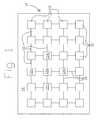
- FIG. 1is a diagrammatic view of a computer array, according to one embodiment of the present invention.
- FIG. 2is a detailed diagram showing a subset of the computers of FIG. 1 and a more detailed view of the interconnecting data buses of FIG. 1 ;
- FIG. 3is a block diagram depicting a general layout of one of the computers of FIGS. 1 and 2 ;
- FIG. 4is a diagrammatic representation of an instruction word according to the present inventive application.
- FIG. 5is a schematic representation of the slot sequencer 42 of FIG. 3 ;
- FIG. 6is a flow diagram depicting an example of the present inventive method.
- a known mode for carrying out the inventionis an array of individual computers.
- the arrayis depicted in a diagrammatic view in FIG. 1 and is designated therein by the general reference character 10 .
- the computer array 10has a plurality (twenty-four in the example shown) of computers 12 (sometimes also referred to as “cores” or “nodes” in the example of an array). In the example shown, all of the computers 12 are located on a single die 14 . According to the present invention, each of the computers 12 is a generally independently functioning computer, as will be discussed in more detail hereinafter.
- the computers 12are interconnected by a plurality (the quantities of which will be discussed in more detail hereinafter) of interconnecting data buses 16 .
- the data buses 16are bidirectional asynchronous high speed parallel data buses, although it is within the scope of the invention that other interconnecting means might be employed for the purpose.
- the individual computers 12In the present embodiment of the array 10 , not only is data communication between the computers 12 asynchronous, the individual computers 12 also operate in an internally asynchronous mode. This has been found by the inventor to provide important advantages. For example, since a clock signal does not have to be distributed throughout the computer array 10 , a great deal of power is saved. Furthermore, not having to distribute a clock signal eliminates many timing problems that could limit the size of the array 10 or cause other known difficulties.
- Such additional componentsinclude power buses, external connection pads, and other such common aspects of a microprocessor chip.
- Computer 12 eis an example of one of the computers 12 that is not on the periphery of the array 10 . That is, computer 12 e has four orthogonally adjacent computers 12 a , 12 b , 12 c and 12 d . This grouping of computers 12 a through 12 e will be used hereinafter in relation to a more detailed discussion of the communications between the computers 12 of the array 10 . As can be seen in the view of FIG. 1 , interior computers such as computer 12 e will have four other computers 12 with which they can directly communicate via the buses 16 . In the following discussion, the principles discussed will apply to all of the computers 12 except that the computers 12 on the periphery of the array 10 will be in direct communication with only three or, in the case of the corner computers 12 , only two other of the computers 12 .
- FIG. 2is a more detailed view of a portion of FIG. 1 showing only some of the computers 12 and, in particular, computers 12 a through 12 e , inclusive.
- the view of FIG. 2also reveals that the data buses 16 each have two communications status lines, which include a read line 18 and a write line 20 , and a plurality (eighteen in this example) of data lines 22 .
- the data lines 22are capable of transferring all the bits of one eighteen-bit instruction word generally simultaneously in parallel.
- some of the computers 12are mirror images of adjacent computers. However, whether the computers 12 are all oriented identically or as mirror images of adjacent computers is not an aspect of this presently described invention. Therefore, in order to better describe this invention, this potential complication will not be discussed further herein.
- a computer 12such as the computer 12 e can set one, two, three or all four of its read lines 18 such that it is prepared to receive data from the respective one, two, three or all four adjacent computers 12 .
- a computer 12it is also possible for a computer 12 to set one, two, three or all four of its write lines 20 high.
- the receiving computermay try to set the write line 20 low slightly before the sending computer 12 releases (stops pulling high) its write line 20 . In such an instance, as soon as the sending computer 12 releases its write line 20 the write line 20 will be pulled low by the receiving computer 12 e.
- computer 12 ewas described as setting one or more of its read lines 18 high before an adjacent computer (selected from one or more of the computers 12 a , 12 b , 12 c or 12 d ) has set its write line 20 high.
- this processcan certainly occur in the opposite order. For example, if the computer 12 e were attempting to write to the computer 12 a , then computer 12 e would set the write line 20 between computer 12 e and computer 12 a to high. If the read line 18 between computer 12 e and computer 12 a has then not already been set to high by computer 12 a , then computer 12 e will simply wait until computer 12 a does set that read line 20 high.
- the receiving computer 12sets both the read line 18 and the write line 20 between the two computers ( 12 e and 12 a in this example) to low as soon as the sending computer 12 e releases it.
- the computers 12there may be several potential means and/or methods to cause the computers 12 to function as described above.
- the computers 12so behave simply because they are operating generally asynchronously internally (in addition to transferring data there-between in the asynchronous manner described). That is, instructions are completed sequentially. When either a write or read instruction occurs, there can be no further action until that instruction is completed (or, perhaps alternatively, until it is aborted, as by a “reset” or the like). There is no regular clock pulse, in the prior art sense.
- a pulseis generated to accomplish a next instruction only when the instruction being executed either is not a read or write type instruction (given that a read or write type instruction would require completion by another entity) or else when the read or write type operation is, in fact, completed.
- FIG. 3is a block diagram depicting the general layout of an example of one of the computers 12 of FIGS. 1 and 2 .
- each of the computers 12is a generally self contained computer having its own RAM 24 and ROM 26 .
- the computers 12are also sometimes referred to as individual “cores”, given that they are, in the present example, combined on a single chip.
- a return stack 28Other basic components of the computer 12 are a return stack 28 , an instruction area 30 , an arithmetic logic unit (“ALU” or “processor”) 32 , a data stack 34 and a decode logic section 36 for decoding instructions.
- ALUarithmetic logic unit
- the computers 12are dual stack computers having the data stack 34 and separate return stack 28 .
- the computer 12has four communication ports 38 for communicating with adjacent computers 12 .
- the communication ports 38are tri-state drivers, having an off status, a receive status (for driving signals into the computer 12 ) and a send status (for driving signals out of the computer 12 ).
- the instruction area 30includes a number of registers 40 including, in this example, an A register 40 a , a B register 40 b and a P register 40 c .
- the A register 40 ais a full eighteen-bit register
- the B register 40 b and the P register 40 care nine-bit registers.
- the present computer 12is implemented to execute native Forth language instructions.
- Forth “words”are constructed from the native processor instructions designed into the computer.
- the collection of Forth wordsis known as a “dictionary”. In other languages, this might be known as a “library”.
- the computer 12reads eighteen bits at a time from RAM 24 , ROM 26 or directly from one of the data buses 16 ( FIG. 2 ).
- operand-less instructionssince in Forth most instructions (known as operand-less instructions) obtain their operands directly from the stacks 28 and 34 , they are generally only five bits in length such that up to four instructions can be included in a single eighteen-bit instruction word, with the condition that the last instruction in the group is selected from a limited set of instructions that require only three bits.
- a slot sequencer 42Also depicted in block diagrammatic form in the view of FIG. 3 is a slot sequencer 42 .
- the top two registers in the data stack 34are a T register 44 and an S register 46 .
- FIG. 4is a diagrammatic representation of an instruction word 48 .
- the instruction word 48can actually contain instructions, data, or some combination thereof.
- the instruction word 48consists of eighteen bits 50 . This being a binary computer, each of the bits 50 will be a ‘1’ or a ‘0’.
- the eighteen-bit wide instruction word 48can contain up to four instructions 52 in four slots 54 called slot zero 54 a , slot one 54 b , slot two 54 c and slot three 54 d .
- the eighteen-bit instruction words 48are always read as a whole.
- FIG. 5is a schematic representation of the slot sequencer 42 of FIG. 3 .
- the slot sequencer 42has a plurality (fourteen in this example) of inverters 56 and one NAND gate 58 arranged in a ring, such that a signal is inverted an odd number of times as it travels through the fourteen inverters 56 and the NAND gate 58 .
- a signalis initiated in the slot sequencer 42 when either of the two inputs to an OR gate 60 goes high.
- a first OR gate input 62is derived from a bit i 4 66 ( FIG. 4 ) of the instruction 52 being executed. If bit i 4 is high then that particular instruction 52 is an ALU instruction, and the i 4 bit 66 is ‘1’. When the i 4 bit is ‘1’, then the first OR gate input 62 is high, and the slot sequencer 42 is triggered to initiate a pulse that will cause the execution of the next instruction 52 .
- a signalwill travel around the slot sequencer 42 twice, producing an output at a slot sequencer output 68 each time.
- the relatively wide output from the slot sequencer output 68is provided to a pulse generator 70 (shown in block diagrammatic form) that produces a narrow timing pulse as an output.
- a pulse generator 70shown in block diagrammatic form
- the i 4 bit 66is ‘0’ (low) and the first OR gate input 62 is, therefore, also low.
- the timing of events in a device such as the computers 12is generally quite critical, and this is no exception.
- the output from the OR gate 60must remain high until after the signal has circulated past the NAND gate 58 in order to initiate the second “lap” of the ring. Thereafter, the output from the OR gate 60 will go low during that second “lap” in order to prevent unwanted continued oscillation of the circuit.
- each instruction 52is set according to whether or not that instruction is a read or write type of instruction.
- the remaining bits 50 in the instruction 52provide the remainder of the particular opcode for that instruction.
- one or more of the bitsmay be used to indicate where data is to be read from or written to in that particular computer 12 .
- data to be writtenalways comes from the T register 44 (the top of the data stack 34 ), however data can be selectively read into either the T register 44 or else the instruction area 30 from where it can be executed.
- bits 50will be used to indicate which of the ports 38 , if any, is to be set to read or write. This later operation is optionally accomplished by using one or more bits to designate a register 40 , such as the A register 40 a , the B register, or the like.
- the designated register 40will be preloaded with data having a bit corresponding to each of the ports 38 (and, also, any other potential entity with which the computer 12 may be attempting to communicate, such as memory, an external communications port, or the like.)
- each of four bits in the particular register 40can correspond to each of the up port 38 a , the right port 38 b , the left port 38 c or the down port 38 d . In such case, where there is a ‘1’ at any of those bit locations, communication will be set to proceed through the corresponding port 38 .
- a read opcodemight set more than one port 38 for communication in a single instruction while, although it is possible, it is not anticipated that a write opcode will set more than one port 38 for communication in a single instruction.
- the opcode of the instruction 52will have a ‘0’ at bit position i 4 66 , and so the first OR gate input 62 of the OR gate 60 is low, and so the slot sequencer 42 is not triggered to generate an enabling pulse.
- both the read line 18 and the corresponding write line 20 between computers 12 e and 12 care high, then both lines 18 and 20 will be released by each of the respective computers 12 that is holding it high.
- the sending computer 12 ewill be holding the write line 18 high while the receiving computer 12 c will be holding the read line 20 high).
- the receiving computer 12 cwill pull both lines 18 and 20 low.
- the receiving computer 12 cmay attempt to pull the lines 18 and 20 low before the sending computer 12 e has released the write line 18 .
- any attempt to pull a line 18 or 20 lowwill not actually succeed until that line 18 or 20 is released by the computer 12 that is latching it high.
- each of the computers 12 e and 12 cwill, upon the acknowledge condition, set its own internal acknowledge line 72 high.
- the acknowledge line 72provides the second OR gate input 64 . Since an input to either of the OR gate 60 inputs 62 or 64 will cause the output of the OR gate 60 to go high, this will initiate operation of the slot sequencer 42 in the manner previously described herein, such that the instruction 52 in the next slot 54 of the instruction word 48 will be executed.
- the acknowledge line 72stays high until the next instruction 52 is decoded, in order to prevent spurious addresses from reaching the address bus.
- the present inventive mechanismincludes a method and apparatus for “prefetching” instructions such that the fetch can begin before the end of the execution of all instructions 52 in the instruction word 48 .
- thisalso is not a necessary aspect of the present inventive method and apparatus for asynchronous data communications.
- the inventor believes that a key feature for enabling efficient asynchronous communications between devicesis some sort of acknowledge signal or condition.
- acknowledge signal or conditionIn the prior art, most communication between devices has been clocked and there is no direct way for a sending device to know that the receiving device has properly received the data. Methods such as checksum operations may have been used to attempt to insure that data is correctly received, but the sending device has no direct indication that the operation is completed.
- the present inventive methodprovides the necessary acknowledge condition that allows, or at least makes practical, asynchronous communications between the devices. Furthermore, the acknowledge condition also makes it possible for one or more of the devices to “go to sleep” until the acknowledge condition occurs.
- an acknowledge conditioncould be communicated between the computers 12 by a separate signal being sent between the computers 12 (either over the interconnecting data bus 16 or over a separate signal line), and such an acknowledge signal would be within the scope of this aspect of the present invention.
- the method for acknowledgementdoes not require any additional signal, clock cycle, timing pulse, or any such resource beyond that described, to actually affect the communication.
- FIG. 6is a flow diagram, designated by the reference character 74 , depicting this method example.
- an ‘initiate communication’ operation 76one computer 12 executes an instruction 53 that causes it to attempt to communicate with another computer 12 . This can be either an attempt to write or an attempt to read.
- a ‘set first line high’ operation 78which occurs generally simultaneously with the ‘initiate communication’ operation 76 , either a read line 18 or a write line 20 is set high (depending upon whether the first computer 12 is attempting to read or to write).
- the computer 12doing so will, according the presently described embodiment of the operation, cease operation, as described in detail previously herein.
- a ‘set second line high’ operation 80the second line (either the write line 20 or read line 18 ) is set high by the second computer 12 .
- data(or instructions, or the like) is transmitted and received over the data lines 22 .
- a ‘pull lines low’ operation 84the read line 18 and the write line 20 are released and then pulled low.
- the acknowledge conditioncauses the computers 12 to resume their operation.
- the acknowledge conditioncauses an acknowledge signal 86 ( FIG. 5 ) which, in this case, is simply the “high” condition of the acknowledge line 72 .
- inventive computer array 10 and computer 12While specific examples of the inventive computer array 10 and computer 12 have been discussed therein, it is expected that there will be a great many applications for these which have not yet been envisioned. Indeed, it is one of the advantages of the present invention that the inventive method and apparatus may be adapted to a great variety of uses.
- the inventive computer array 10 , computers 12 and associated method 74are intended to be widely used in a great variety of computer applications. It is expected that it they will be particularly useful in applications where significant computing power is required, and yet power consumption and heat production are important considerations.
- the applicability of the present inventionis such that many types of inter-device computer communications can be improved thereby. It is anticipated that the inventive method, wherein some computers can be allowed to “go to sleep” when not in use, will be used to reduce power consumption, reduce heat production, and improve the efficiency of communication between computers and computerized devices in a great variety of applications and implementations.
Landscapes
- Engineering & Computer Science (AREA)
- Theoretical Computer Science (AREA)
- Physics & Mathematics (AREA)
- General Engineering & Computer Science (AREA)
- General Physics & Mathematics (AREA)
- Multi Processors (AREA)
- Power Sources (AREA)
Abstract
Description
Claims (15)
Priority Applications (54)
| Application Number | Priority Date | Filing Date | Title |
|---|---|---|---|
| US11/355,513US7904695B2 (en) | 2006-02-16 | 2006-02-16 | Asynchronous power saving computer |
| US11/441,818US7934075B2 (en) | 2006-02-16 | 2006-05-26 | Method and apparatus for monitoring inputs to an asyncrhonous, homogenous, reconfigurable computer array |
| US11/441,784US7752422B2 (en) | 2006-02-16 | 2006-05-26 | Execution of instructions directly from input source |
| US11/441,812US7913069B2 (en) | 2006-02-16 | 2006-05-26 | Processor and method for executing a program loop within an instruction word |
| US11/503,372US7617383B2 (en) | 2006-02-16 | 2006-08-11 | Circular register arrays of a computer |
| US11/653,187US7966481B2 (en) | 2006-02-16 | 2007-01-12 | Computer system and method for executing port communications without interrupting the receiving computer |
| TW096105687ATW200809530A (en) | 2006-02-16 | 2007-02-15 | Asynchronous power saving computer |
| DE602007011841TDE602007011841D1 (en) | 2006-02-16 | 2007-02-15 | Execution of instructions directly from the input source |
| AT07250649TATE495491T1 (en) | 2006-02-16 | 2007-02-15 | EXECUTION OF INSTRUCTIONS DIRECTLY FROM THE INPUT SOURCE |
| EP07250647AEP1821211A3 (en) | 2006-02-16 | 2007-02-15 | Cooperative multitasking method in a multiprocessor system |
| EP07250645AEP1821174B9 (en) | 2006-02-16 | 2007-02-15 | Asynchronous power saving computer |
| EP07250644AEP1821198A1 (en) | 2006-02-16 | 2007-02-15 | Circular register arrays of a computer |
| AT07250648TATE512409T1 (en) | 2006-02-16 | 2007-02-15 | ASYNCHRONOUS COMPUTER COMMUNICATION |
| EP07250646AEP1821200B1 (en) | 2006-02-16 | 2007-02-15 | Method and apparatus for handling inputs to a single-chip multiprocessor system |
| TW096105684ATW200813744A (en) | 2006-02-16 | 2007-02-15 | Asynchronous computer communication |
| TW96105677ATW200809612A (en) | 2006-02-16 | 2007-02-15 | Circular register arrays of a computer |
| TW96105683ATW200809529A (en) | 2006-02-16 | 2007-02-15 | Computer system with increased operating efficiency |
| EP07250614AEP1821199B1 (en) | 2006-02-16 | 2007-02-15 | Execution of microloop computer instructions received from an external source |
| DE602007007999TDE602007007999D1 (en) | 2006-02-16 | 2007-02-15 | Asynchronous power-saving computer |
| AT07250645TATE475927T1 (en) | 2006-02-16 | 2007-02-15 | ASYNCHRONOUS POWER-SAVING COMPUTER |
| EP07250648AEP1821217B1 (en) | 2006-02-16 | 2007-02-15 | Asynchronous computer communication |
| AT07250646TATE512400T1 (en) | 2006-02-16 | 2007-02-15 | METHOD AND APPARATUS FOR TREATING INPUTS TO A SINGLE-CHIP MULTI-PROCESSOR SYSTEM |
| EP07250649AEP1821202B1 (en) | 2006-02-16 | 2007-02-15 | Execution of instructions directly from input source |
| JP2008555353AJP2009527808A (en) | 2006-02-16 | 2007-02-16 | Micro loop computer instruction |
| TW096106397ATW200809609A (en) | 2006-02-16 | 2007-02-16 | Microloop computer instructions |
| JP2008555371AJP2009527815A (en) | 2006-02-16 | 2007-02-16 | Computer system with increased operating efficiency |
| TW096106396ATW200809531A (en) | 2006-02-16 | 2007-02-16 | Method and apparatus for monitoring inputs to a computer |
| JP2008555369AJP2009527813A (en) | 2006-02-16 | 2007-02-16 | Asynchronous power saving computer |
| CNA2007800000160ACN101563679A (en) | 2006-02-16 | 2007-02-16 | Method and apparatus for monitoring a computer's inputs for incoming instructions |
| PCT/US2007/004083WO2007098026A2 (en) | 2006-02-16 | 2007-02-16 | Method and apparatus for monitoring inputs to a computer |
| JP2008555355AJP2009527810A (en) | 2006-02-16 | 2007-02-16 | Asynchronous computer communication |
| KR1020077009922AKR20090016644A (en) | 2006-02-16 | 2007-02-16 | Computer system increases operational efficiency |
| PCT/US2007/004031WO2007098007A2 (en) | 2006-02-16 | 2007-02-16 | Asynchronous computer communication |
| PCT/US2007/004081WO2007098024A2 (en) | 2006-02-16 | 2007-02-16 | Allocation of resources among an array of computers |
| EP07750884AEP1984836A4 (en) | 2006-02-16 | 2007-02-16 | Allocation of resources among an array of computers |
| JP2008555372AJP2009527816A (en) | 2006-02-16 | 2007-02-16 | Method and apparatus for monitoring input to a computer |
| TW096106394ATW200809613A (en) | 2006-02-16 | 2007-02-16 | Execution of instructions directly from input source |
| CNA2007800000156ACN101366003A (en) | 2006-02-16 | 2007-02-16 | Microloop computer instructions |
| PCT/US2007/004082WO2007098025A2 (en) | 2006-02-16 | 2007-02-16 | Computer system with increased operating efficiency |
| CNA2007800000137ACN101479714A (en) | 2006-02-16 | 2007-02-16 | Execution of instructions directly from input source |
| PCT/US2007/004030WO2007098006A2 (en) | 2006-02-16 | 2007-02-16 | Execution of instructions directly from input source |
| KR1020077009920AKR20090016642A (en) | 2006-02-16 | 2007-02-16 | Asynchronous computer communication |
| KR1020077009925AKR20090016645A (en) | 2006-02-16 | 2007-02-16 | Methods and devices for monitoring computer input |
| CNA200780000018XACN101454755A (en) | 2005-05-26 | 2007-02-16 | Computer system with increased operating efficiency |
| KR1020077009921AKR20090016643A (en) | 2006-02-16 | 2007-02-16 | Asynchronous sleep computer |
| JP2008555354AJP2009527809A (en) | 2006-02-16 | 2007-02-16 | Executing instructions directly from the input source |
| KR1020087022319AKR20090003217A (en) | 2006-02-16 | 2007-02-16 | Allocation of Resources Between Arrays of Computers |
| PCT/US2007/004029WO2007098005A2 (en) | 2006-02-16 | 2007-02-16 | Microloop computer instructions |
| KR1020077009923AKR20090017390A (en) | 2006-02-16 | 2007-02-16 | Micro loop computer instruction |
| JP2008555370AJP2009527814A (en) | 2006-02-16 | 2007-02-16 | Allocating resources between arrays of computers |
| KR1020077009924AKR20090004394A (en) | 2006-02-16 | 2007-02-16 | Execution of Direct Commands from Input Sources |
| PCT/US2007/004080WO2007098023A2 (en) | 2006-02-16 | 2007-02-16 | Asynchronous power saving computer |
| US12/803,652US20100281238A1 (en) | 2006-02-16 | 2010-07-01 | Execution of instructions directly from input source |
| US13/053,062US8468323B2 (en) | 2006-02-16 | 2011-03-21 | Clockless computer using a pulse generator that is triggered by an event other than a read or write instruction in place of a clock |
Applications Claiming Priority (1)
| Application Number | Priority Date | Filing Date | Title |
|---|---|---|---|
| US11/355,513US7904695B2 (en) | 2006-02-16 | 2006-02-16 | Asynchronous power saving computer |
Related Parent Applications (3)
| Application Number | Title | Priority Date | Filing Date |
|---|---|---|---|
| US11/441,818Continuation-In-PartUS7934075B2 (en) | 2006-02-16 | 2006-05-26 | Method and apparatus for monitoring inputs to an asyncrhonous, homogenous, reconfigurable computer array |
| US11/441,818DivisionUS7934075B2 (en) | 2006-02-16 | 2006-05-26 | Method and apparatus for monitoring inputs to an asyncrhonous, homogenous, reconfigurable computer array |
| US12/803,652DivisionUS20100281238A1 (en) | 2006-02-16 | 2010-07-01 | Execution of instructions directly from input source |
Related Child Applications (4)
| Application Number | Title | Priority Date | Filing Date |
|---|---|---|---|
| US11/441,818Continuation-In-PartUS7934075B2 (en) | 2006-02-16 | 2006-05-26 | Method and apparatus for monitoring inputs to an asyncrhonous, homogenous, reconfigurable computer array |
| US11/441,812Continuation-In-PartUS7913069B2 (en) | 2006-02-16 | 2006-05-26 | Processor and method for executing a program loop within an instruction word |
| US11/441,784Continuation-In-PartUS7752422B2 (en) | 2006-02-16 | 2006-05-26 | Execution of instructions directly from input source |
| US11/653,187Continuation-In-PartUS7966481B2 (en) | 2006-02-16 | 2007-01-12 | Computer system and method for executing port communications without interrupting the receiving computer |
Publications (2)
| Publication Number | Publication Date |
|---|---|
| US20070192646A1 US20070192646A1 (en) | 2007-08-16 |
| US7904695B2true US7904695B2 (en) | 2011-03-08 |
Family
ID=38370171
Family Applications (1)
| Application Number | Title | Priority Date | Filing Date |
|---|---|---|---|
| US11/355,513Expired - Fee RelatedUS7904695B2 (en) | 2005-05-26 | 2006-02-16 | Asynchronous power saving computer |
Country Status (2)
| Country | Link |
|---|---|
| US (1) | US7904695B2 (en) |
| CN (4) | CN101366003A (en) |
Cited By (1)
| Publication number | Priority date | Publication date | Assignee | Title |
|---|---|---|---|---|
| US20100111146A1 (en)* | 2008-11-04 | 2010-05-06 | Renesas Technology Corp. | Communication device and communication system |
Families Citing this family (10)
| Publication number | Priority date | Publication date | Assignee | Title |
|---|---|---|---|---|
| US7937557B2 (en)* | 2004-03-16 | 2011-05-03 | Vns Portfolio Llc | System and method for intercommunication between computers in an array |
| US7904615B2 (en) | 2006-02-16 | 2011-03-08 | Vns Portfolio Llc | Asynchronous computer communication |
| US7966481B2 (en) | 2006-02-16 | 2011-06-21 | Vns Portfolio Llc | Computer system and method for executing port communications without interrupting the receiving computer |
| KR101738641B1 (en) | 2010-12-17 | 2017-05-23 | 삼성전자주식회사 | Apparatus and method for compilation of program on multi core system |
| CN102650981A (en)* | 2011-02-25 | 2012-08-29 | 西安邮电学院 | Synchronous structure between programmable operational level parallel units |
| TWI613546B (en)* | 2013-03-28 | 2018-02-01 | 威盛電子股份有限公司 | Universal serial bus hub and control method thereof |
| US10216253B2 (en) | 2013-03-28 | 2019-02-26 | Via Technologies, Inc. | Universal serial bus hub and control method thereof |
| CN109388606A (en)* | 2018-09-27 | 2019-02-26 | 浙江大学 | Restructural series bus controller in a kind of chip |
| CN110457072A (en)* | 2019-06-25 | 2019-11-15 | 珠海格力电器股份有限公司 | Method, device, equipment and computer readable medium for preventing system hang-up |
| CN111353752B (en)* | 2019-11-05 | 2024-04-19 | 泰康保险集团股份有限公司 | Flow processing method and device, electronic equipment and storage medium |
Citations (124)
| Publication number | Priority date | Publication date | Assignee | Title |
|---|---|---|---|---|
| US3868677A (en) | 1972-06-21 | 1975-02-25 | Gen Electric | Phase-locked voltage-to-digital converter |
| US4215401A (en) | 1978-09-28 | 1980-07-29 | Environmental Research Institute Of Michigan | Cellular digital array processor |
| GB2154343A (en) | 1984-02-16 | 1985-09-04 | Xerox Corp | Adaptive self repairing processor array |
| US4593351A (en) | 1981-06-12 | 1986-06-03 | International Business Machines Corporation | High speed machine for the physical design of very large scale integrated circuits |
| US4665494A (en) | 1982-12-17 | 1987-05-12 | Victor Company Of Japan, Limited | Spectrum display device for audio signals |
| US4672331A (en) | 1983-06-21 | 1987-06-09 | Cushing Vincent J | Signal conditioner for electromagnetic flowmeter |
| US4739474A (en) | 1983-03-10 | 1988-04-19 | Martin Marietta Corporation | Geometric-arithmetic parallel processor |
| US4742511A (en) | 1985-06-13 | 1988-05-03 | Texas Instruments Incorporated | Method and apparatus for routing packets in a multinode computer interconnect network |
| US4789927A (en) | 1986-04-07 | 1988-12-06 | Silicon Graphics, Inc. | Interleaved pipeline parallel processing architecture |
| US4868745A (en) | 1986-05-30 | 1989-09-19 | Hewlett-Packard Company | Data processing system and method for the direct and indirect execution of uniformly structured object types |
| US4961167A (en)* | 1988-08-26 | 1990-10-02 | Mitsubishi Denki Kabushiki Kaisha | Substrate bias generator in a dynamic random access memory with auto/self refresh functions and a method of generating a substrate bias therein |
| US5021947A (en) | 1986-03-31 | 1991-06-04 | Hughes Aircraft Company | Data-flow multiprocessor architecture with three dimensional multistage interconnection network for efficient signal and data processing |
| CN1051995A (en) | 1989-11-21 | 1991-06-05 | 德国Itt工业股份有限公司 | Data-driven array processor |
| US5029124A (en) | 1988-05-17 | 1991-07-02 | Digital Equipment Corporation | Method and apparatus for providing high speed parallel transfer of bursts of data |
| US5159338A (en) | 1990-11-30 | 1992-10-27 | Kabushiki Kaisha Toshiba | Sampling frequency conversion apparatus |
| US5386585A (en)* | 1993-02-03 | 1995-01-31 | Intel Corporation | Self-timed data pipeline apparatus using asynchronous stages having toggle flip-flops |
| US5434989A (en) | 1991-02-19 | 1995-07-18 | Matsushita Electric Industrial Co., Ltd. | Cache memory for efficient access with address selectors |
| US5475856A (en) | 1991-11-27 | 1995-12-12 | International Business Machines Corporation | Dynamic multi-mode parallel processing array |
| JP2509678B2 (en) | 1987-07-08 | 1996-06-26 | エイ・ティ・アンド・ティ・コーポレーション | Computer |
| EP0724221A2 (en) | 1995-01-26 | 1996-07-31 | International Business Machines Corporation | Method and apparatus for executing dissimilar seq. of instructions in the processor of a single-instruction-multiple data (SIMD) computer |
| US5550489A (en)* | 1995-09-29 | 1996-08-27 | Quantum Corporation | Secondary clock source for low power, fast response clocking |
| GB2299422A (en) | 1995-03-30 | 1996-10-02 | Sony Uk Ltd | Object code allocation in multiple processor systems |
| US5581767A (en) | 1993-06-16 | 1996-12-03 | Nippon Sheet Glass Co., Ltd. | Bus structure for multiprocessor system having separated processor section and control/memory section |
| US5630154A (en) | 1994-10-11 | 1997-05-13 | Hughes Aircraft Company | Programmable systolic array system arranged in a found arrangement for passing data through programmable number of cells in a time interleaved manner |
| JP2543306Y2 (en) | 1990-06-12 | 1997-08-06 | 市光工業株式会社 | Direct optics for vehicle headlamps |
| US5673423A (en) | 1988-02-02 | 1997-09-30 | Tm Patents, L.P. | Method and apparatus for aligning the operation of a plurality of processors |
| US5737628A (en) | 1993-12-10 | 1998-04-07 | Cray Research, Inc. | Multiprocessor computer system with interleaved processing element nodes |
| US5740463A (en) | 1994-07-22 | 1998-04-14 | Mitsubishi Denki Kabushiki Kaisha | Information processing system and method of computation performed with an information processing system |
| US5765015A (en) | 1990-11-13 | 1998-06-09 | International Business Machines Corporation | Slide network for an array processor |
| US5832291A (en) | 1995-12-15 | 1998-11-03 | Raytheon Company | Data processor with dynamic and selectable interconnections between processor array, external memory and I/O ports |
| US5867330A (en) | 1994-11-11 | 1999-02-02 | Canon Kabushiki Kaisha | Reproducing apparatus detecting pilot signals by binary data processing |
| US5937202A (en) | 1993-02-11 | 1999-08-10 | 3-D Computing, Inc. | High-speed, parallel, processor architecture for front-end electronics, based on a single type of ASIC, and method use thereof |
| US6057791A (en) | 1998-02-18 | 2000-05-02 | Oasis Design, Inc. | Apparatus and method for clocking digital and analog circuits on a common substrate to enhance digital operation and reduce analog sampling error |
| US6081215A (en) | 1998-07-06 | 2000-06-27 | Motorola, Inc. | High speed interlaced analog interface |
| US6092183A (en) | 1994-03-16 | 2000-07-18 | Hitachi, Ltd. | Data processor for processing a complex instruction by dividing it into executing units |
| US6094030A (en) | 1999-05-13 | 2000-07-25 | Deltatee Enterprises Ltd. | Resistance and charging monitor within a standby battery bank |
| US6145072A (en)* | 1993-08-12 | 2000-11-07 | Hughes Electronics Corporation | Independently non-homogeneously dynamically reconfigurable two dimensional interprocessor communication topology for SIMD multi-processors and apparatus for implementing same |
| US6192388B1 (en) | 1996-06-20 | 2001-02-20 | Avid Technology, Inc. | Detecting available computers to participate in computationally complex distributed processing problem |
| US6219685B1 (en) | 1998-09-04 | 2001-04-17 | Intel Corporation | Method to detect IEEE overflow and underflow conditions |
| US6232905B1 (en) | 1999-03-08 | 2001-05-15 | Agere Systems Guardian Corp. | Clocking technique for reducing sampling noise in an analog-to-digital converter |
| US6233670B1 (en) | 1991-06-17 | 2001-05-15 | Mitsubishi Denki Kabushiki Kaisha | Superscalar processor with direct result bypass between execution units having comparators in execution units for comparing operand and result addresses and activating result bypassing |
| US6236645B1 (en) | 1998-03-09 | 2001-05-22 | Broadcom Corporation | Apparatus for, and method of, reducing noise in a communications system |
| US6308229B1 (en)* | 1998-08-28 | 2001-10-23 | Theseus Logic, Inc. | System for facilitating interfacing between multiple non-synchronous systems utilizing an asynchronous FIFO that uses asynchronous logic |
| US6307425B1 (en)* | 1996-07-18 | 2001-10-23 | Micron Technology, Inc. | Clocking scheme and charge transfer switch for increasing the efficiency of a charge pump or other circuit |
| US20020004912A1 (en) | 1990-06-01 | 2002-01-10 | Amphus, Inc. | System, architecture, and method for logical server and other network devices in a dynamically configurable multi-server network environment |
| US20020019951A1 (en) | 2000-08-02 | 2002-02-14 | Masahito Kubo | Timer adjusting system |
| US6367005B1 (en) | 1998-04-21 | 2002-04-02 | Idea Corporation Of Delaware | System and method for synchronizing a register stack engine (RSE) and backing memory image with a processor's execution of instructions during a state saving context switch |
| US6388600B1 (en) | 2000-11-13 | 2002-05-14 | Trw Inc. | Asynchronous superconductor serial multiply-accumulator |
| US6404274B1 (en)* | 1998-04-09 | 2002-06-11 | Kabushiki Kaisha Toshiba | Internal voltage generating circuit capable of generating variable multi-level voltages |
| US6404663B2 (en)* | 1999-06-14 | 2002-06-11 | Fujitsu Limited | Semiconductor integrated circuit having testing mode for modifying operation timing |
| US20020186159A1 (en) | 2001-05-03 | 2002-12-12 | Mario Reinhold | Amplitude detection for controlling the decision instant for sampling as a data flow |
| US6502141B1 (en) | 1999-12-14 | 2002-12-31 | International Business Machines Corporation | Method and system for approximate, monotonic time synchronization for a multiple node NUMA system |
| US20030005168A1 (en) | 2001-06-29 | 2003-01-02 | Leerssen Scott Alan | System and method for auditing system call events with system call wrappers |
| US20030009502A1 (en) | 2001-06-29 | 2003-01-09 | Nec Corporation | Complex vector operation processor with pipeline processing function and system using the same |
| US6507947B1 (en) | 1999-08-20 | 2003-01-14 | Hewlett-Packard Company | Programmatic synthesis of processor element arrays |
| US6522282B1 (en) | 2001-11-07 | 2003-02-18 | Telefonaktiebolaget Lm Ericsson (Publ) | Estimation of timing offsets in parallel A/D converters |
| US20030035549A1 (en) | 1999-11-29 | 2003-02-20 | Bizjak Karl M. | Signal processing system and method |
| US6542105B2 (en) | 2000-12-18 | 2003-04-01 | Canon Kabushiki Kaisha | A/D converter |
| US20030065905A1 (en) | 2001-10-01 | 2003-04-03 | Nec Corporation | Parallel computation processor, parallel computation control method and program thereof |
| US6560716B1 (en)* | 1999-11-10 | 2003-05-06 | Lsi Logic Corporation | System for measuring delay of digital signal using clock generator and delay unit wherein a set of digital elements of clock generator identical to a set of digital elements of delay unit |
| US20030113031A1 (en) | 1997-04-15 | 2003-06-19 | Wal Gooitzen Siemen Van Der | Parallel pipeline image processing system |
| US20030135710A1 (en) | 2002-01-17 | 2003-07-17 | Farwell William D. | Reconfigurable processor architectures |
| US20030179123A1 (en) | 2002-03-22 | 2003-09-25 | Devilbiss Alan D. | Analog-to-digital conversion using a counter |
| US6636122B2 (en) | 2001-10-09 | 2003-10-21 | Zilog, Inc. | Analog frequency locked loop with digital oversampling feedback control and filter |
| US6647027B1 (en)* | 1999-11-10 | 2003-11-11 | Lsi Logic Corporation | Method and apparatus for multi-channel data delay equalization |
| US6657462B2 (en)* | 2001-09-24 | 2003-12-02 | Broadcom Corporation | Conditional clock buffer circuit |
| US6671112B2 (en) | 1995-08-11 | 2003-12-30 | Fujitsu Limited | Semiconductor integrated circuit device |
| US20040030859A1 (en) | 2002-06-26 | 2004-02-12 | Doerr Michael B. | Processing system with interspersed processors and communication elements |
| US6732253B1 (en) | 2000-11-13 | 2004-05-04 | Chipwrights Design, Inc. | Loop handling for single instruction multiple datapath processor architectures |
| US20040098707A1 (en) | 2002-11-18 | 2004-05-20 | Microsoft Corporation | Generic wrapper scheme |
| US20040095264A1 (en) | 2002-11-14 | 2004-05-20 | Thomas John Carl | Power converter circuitry and method |
| US6782468B1 (en) | 1998-12-15 | 2004-08-24 | Nec Corporation | Shared memory type vector processing system, including a bus for transferring a vector processing instruction, and control method thereof |
| US20040215929A1 (en) | 2003-04-28 | 2004-10-28 | International Business Machines Corporation | Cross-chip communication mechanism in distributed node topology |
| US20040250046A1 (en) | 2003-03-31 | 2004-12-09 | Gonzalez Ricardo E. | Systems and methods for software extensible multi-processing |
| US20050015572A1 (en) | 2003-07-09 | 2005-01-20 | Hiroshi Tanaka | Semiconductor integrated circuit |
| US20050027548A1 (en) | 2003-07-31 | 2005-02-03 | Jacobs Philip C. | Cost minimization of services provided by multiple service providers |
| US20050034029A1 (en) | 1999-01-29 | 2005-02-10 | Intermec Ip Corp. | Remote anomaly diagnosis and reconfiguration of an automatic data collection device platform over a telecommunications network |
| US6898721B2 (en) | 2001-06-22 | 2005-05-24 | Gallitzin Allegheny Llc | Clock generation systems and methods |
| US20050182581A1 (en) | 2002-05-14 | 2005-08-18 | Analysis And Measurement Services Corporation | Testing of wire systems and end devices installed in industrial processes |
| US6937538B2 (en)* | 2000-02-02 | 2005-08-30 | Broadcom Corporation | Asynchronously resettable decoder for a semiconductor memory |
| US20050196060A1 (en) | 2004-03-03 | 2005-09-08 | Demin Wang | Curved wavelet transform for image and video compression |
| US20050206648A1 (en) | 2004-03-16 | 2005-09-22 | Perry Ronald N | Pipeline and cache for processing data progressively |
| US20050228904A1 (en) | 2004-03-16 | 2005-10-13 | Moore Charles H | Computer processor array |
| US20050237083A1 (en) | 2003-07-31 | 2005-10-27 | Actel Corporation, A California Corporation | Programmable system on a chip |
| US6966002B1 (en) | 1999-04-30 | 2005-11-15 | Trymedia Systems, Inc. | Methods and apparatus for secure distribution of software |
| US20050257037A1 (en) | 2003-04-04 | 2005-11-17 | Arm Limited | Controlling execution of a block of program instructions within a computer processing system |
| US20050262278A1 (en) | 2004-05-20 | 2005-11-24 | Schmidt Dominik J | Integrated circuit with a plurality of host processor family types |
| US6970895B2 (en) | 2001-10-01 | 2005-11-29 | Koninklijke Philips Electronics N.V. | Programmable delay indexed data path register file for array processing |
| US20060059377A1 (en) | 2001-04-18 | 2006-03-16 | Sherburne Robert W Jr | Low power clocking systems and methods |
| US20060082445A1 (en) | 1996-05-13 | 2006-04-20 | O'toole James E | Radio frequency data communications device |
| US20060097901A1 (en) | 2004-10-08 | 2006-05-11 | Dieter Draxelmayr | Analog-to-digital converter operable with staggered timing |
| US7084793B2 (en) | 2003-01-15 | 2006-08-01 | Infineon Technologies Ag | Method and device for estimating time errors in time interleaved A/D converter system |
| US7089438B2 (en) | 2002-06-25 | 2006-08-08 | Micron Technology, Inc. | Circuit, system and method for selectively turning off internal clock drivers |
| US20060212867A1 (en) | 2005-03-17 | 2006-09-21 | Microsoft Corporation | Determining an actual amount of time a processor consumes in executing a portion of code |
| US20060218375A1 (en) | 2003-02-12 | 2006-09-28 | Swarztrauber Paul N | System and method of transferring data between a massive number of processors |
| US20060224831A1 (en) | 2005-04-04 | 2006-10-05 | Toshiba America Electronic Components | Systems and methods for loading data into the cache of one processor to improve performance of another processor in a multiprocessor system |
| US7131113B2 (en) | 2002-12-12 | 2006-10-31 | International Business Machines Corporation | System and method on generating multi-dimensional trace files and visualizing them using multiple Gantt charts |
| US20060248360A1 (en) | 2001-05-18 | 2006-11-02 | Fung Henry T | Multi-server and multi-CPU power management system and method |
| US20060259743A1 (en)* | 2005-05-10 | 2006-11-16 | Masakazu Suzuoki | Methods and apparatus for power management in a computing system |
| US20060271764A1 (en) | 2005-05-24 | 2006-11-30 | Coresonic Ab | Programmable digital signal processor including a clustered SIMD microarchitecture configured to execute complex vector instructions |
| US20060279970A1 (en) | 2002-11-14 | 2006-12-14 | Kent Kernahan | Switching power converter controller |
| US20060279445A1 (en) | 2005-06-13 | 2006-12-14 | Kinyua Martin K | System and method for improved time-interleaved analog-to-digital converter arrays |
| US20060279969A1 (en) | 2004-07-27 | 2006-12-14 | Silicon Laboratories Inc. | Distributed power supply system with separate SYNC control for controlling remote digital DC/DC converters |
| US7157934B2 (en) | 2003-08-19 | 2007-01-02 | Cornell Research Foundation, Inc. | Programmable asynchronous pipeline arrays |
| US7162573B2 (en) | 2003-06-25 | 2007-01-09 | Intel Corporation | Communication registers for processing elements |
| US20070035611A1 (en) | 2005-07-27 | 2007-02-15 | Chao-Hung Wu | Mobile audio/video data transmission system and method for the same |
| US20070036150A1 (en) | 1998-04-03 | 2007-02-15 | Pounds Gregory E | Systems and methods for TDM/packet communications using telephony station cards including voltage generators |
| US20070041438A1 (en) | 2004-01-30 | 2007-02-22 | Sony Corporation | Sampling rate conversion device and method, and audio device |
| US20070070079A1 (en) | 2002-01-17 | 2007-03-29 | University Of Washington | Programmable 3d graphics pipeline for multimedia applications |
| US20070153953A1 (en) | 2006-01-04 | 2007-07-05 | Matthias Garzarolli | Phase-Locked Loop |
| US7249357B2 (en) | 2001-08-20 | 2007-07-24 | Silicon Graphics, Inc. | Transparent distribution and execution of data in a multiprocessor environment |
| US7255476B2 (en)* | 2004-04-14 | 2007-08-14 | International Business Machines Corporation | On chip temperature measuring and monitoring circuit and method |
| US20070192504A1 (en) | 2006-02-16 | 2007-08-16 | Moore Charles H | Asynchronous computer communication |
| US7263624B2 (en) | 2000-05-12 | 2007-08-28 | Altera Corporation | Methods and apparatus for power control in a scalable array of processor elements |
| US7265640B1 (en)* | 2004-12-23 | 2007-09-04 | Xilinx, Inc. | Circuit approach for common mode control in high-frequency clocks |
| US20070226457A1 (en) | 2006-02-16 | 2007-09-27 | Moore Charles H | Computer system with increased operating efficiency |
| US7319355B2 (en)* | 2006-01-03 | 2008-01-15 | Taiwan Semiconductor Manufacturing Co., Ltd. | Pulse generator |
| US7380100B2 (en) | 2001-09-07 | 2008-05-27 | Ipflex Inc. | Data processing system and control method utilizing a plurality of date transfer means |
| US7386689B2 (en)* | 2000-08-31 | 2008-06-10 | Micron Technology, Inc. | Method and apparatus for connecting a massively parallel processor array to a memory array in a bit serial manner |
| US7403055B2 (en)* | 2005-08-31 | 2008-07-22 | Infineon Technologies Ag | Duty cycle detector with first and second oscillating signals |
| US20080270648A1 (en) | 2007-04-27 | 2008-10-30 | Technology Properties Limited | System and method for multi-port read and write operations |
| US7471643B2 (en) | 2002-07-01 | 2008-12-30 | Panasonic Corporation | Loosely-biased heterogeneous reconfigurable arrays |
| US7512728B2 (en) | 1998-08-31 | 2009-03-31 | Axis Systems, Inc | Inter-chip communication system |
| US7528756B2 (en) | 2007-03-22 | 2009-05-05 | Vns Portfolio Llc | Analog-to-digital converter system with increased sampling frequency |
Family Cites Families (38)
| Publication number | Priority date | Publication date | Assignee | Title |
|---|---|---|---|---|
| US4215422A (en)* | 1978-05-22 | 1980-07-29 | International Business Machines Corporation | Selectively modifiable phrase storage for a typewriter |
| US4462074A (en)* | 1981-11-19 | 1984-07-24 | Codex Corporation | Do loop circuit |
| US4821231A (en)* | 1983-04-18 | 1989-04-11 | Motorola, Inc. | Method and apparatus for selectively evaluating an effective address for a coprocessor |
| US4589067A (en)* | 1983-05-27 | 1986-05-13 | Analogic Corporation | Full floating point vector processor with dynamically configurable multifunction pipelined ALU |
| ATE94999T1 (en)* | 1984-11-21 | 1993-10-15 | Harris Corp | MICROPROCESSOR FOR FORTH-LIKE LANGUAGE. |
| US4984151A (en)* | 1985-03-01 | 1991-01-08 | Advanced Micro Devices, Inc. | Flexible, next-address generation microprogram sequencer |
| DE3901457A1 (en)* | 1989-01-19 | 1990-08-02 | Strahlen Umweltforsch Gmbh | METHOD FOR ADDRESS AREA MONITORING IN REAL-TIME DATA PROCESSING DEVICES |
| DE4019040A1 (en)* | 1990-06-14 | 1991-12-19 | Philips Patentverwaltung | MULTIPLE COMPUTER SYSTEM |
| US5390304A (en)* | 1990-09-28 | 1995-02-14 | Texas Instruments, Incorporated | Method and apparatus for processing block instructions in a data processor |
| US5590345A (en)* | 1990-11-13 | 1996-12-31 | International Business Machines Corporation | Advanced parallel array processor(APAP) |
| US5218682A (en)* | 1991-05-10 | 1993-06-08 | Chrysler Corporation | Two-way handshake circuit and method for communication between processors |
| DE69229657T2 (en)* | 1991-06-19 | 1999-12-02 | Hewlett-Packard Co., Palo Alto | Co-processor supporting architecture for a processor that has no additional processor capability |
| CA2078315A1 (en)* | 1991-09-20 | 1993-03-21 | Christopher L. Reeve | Parallel processing apparatus and method for utilizing tiling |
| US5473271A (en)* | 1993-02-09 | 1995-12-05 | Dallas Semiconductor Corporation | Microprocessor output driver |
| US5535417A (en)* | 1993-09-27 | 1996-07-09 | Hitachi America, Inc. | On-chip DMA controller with host computer interface employing boot sequencing and address generation schemes |
| US5893148A (en)* | 1994-03-03 | 1999-04-06 | International Business Machines Corporation | System and method for allocating cache memory storage space |
| US5706491A (en)* | 1994-10-18 | 1998-01-06 | Cyrix Corporation | Branch processing unit with a return stack including repair using pointers from different pipe stages |
| US5727194A (en)* | 1995-06-07 | 1998-03-10 | Hitachi America, Ltd. | Repeat-bit based, compact system and method for implementing zero-overhead loops |
| US5752259A (en)* | 1996-03-26 | 1998-05-12 | Advanced Micro Devices, Inc. | Instruction cache configured to provide instructions to a microprocessor having a clock cycle time less than a cache access time of said instruction cache |
| US5911082A (en)* | 1997-02-25 | 1999-06-08 | Audio Digitalimaging Inc. | Parallel processing building block chip |
| GB9704068D0 (en)* | 1997-02-27 | 1997-04-16 | Sgs Thomson Microelectronics | Trigger sequencing controller |
| US6023753A (en)* | 1997-06-30 | 2000-02-08 | Billion Of Operations Per Second, Inc. | Manifold array processor |
| US6381682B2 (en)* | 1998-06-10 | 2002-04-30 | Compaq Information Technologies Group, L.P. | Method and apparatus for dynamically sharing memory in a multiprocessor system |
| US6173389B1 (en)* | 1997-12-04 | 2001-01-09 | Billions Of Operations Per Second, Inc. | Methods and apparatus for dynamic very long instruction word sub-instruction selection for execution time parallelism in an indirect very long instruction word processor |
| KR100252136B1 (en)* | 1997-12-29 | 2000-04-15 | 윤종용 | Circuit for controlling execution of repetition structure in a dsp chip |
| US7028163B2 (en)* | 1998-06-22 | 2006-04-11 | Samsung Electronics, Co., Ltd. | Apparatus for controlling multi-word stack operations using a multi-bank stack in digital data processors |
| US6353880B1 (en)* | 1998-07-22 | 2002-03-05 | Scenix Semiconductor, Inc. | Four stage pipeline processing for a microcontroller |
| US6507649B1 (en)* | 1998-12-18 | 2003-01-14 | Ericsson Inc. | Mechanism and method for distributing ISUP stacks over multiple loosely coupled processors |
| FR2789501B1 (en)* | 1999-02-09 | 2001-04-13 | St Microelectronics Sa | METHOD AND DEVICE FOR REDUCING THE CONSUMPTION OF A MICROCONTROLLER |
| US6725361B1 (en)* | 2000-06-16 | 2004-04-20 | Transmeta Corporation | Method and apparatus for emulating a floating point stack in a translation process |
| DE10102202A1 (en)* | 2001-01-18 | 2002-08-08 | Infineon Technologies Ag | Microprocessor circuit for portable data carriers |
| US6874079B2 (en)* | 2001-07-25 | 2005-03-29 | Quicksilver Technology | Adaptive computing engine with dataflow graph based sequencing in reconfigurable mini-matrices of composite functional blocks |
| US6845412B1 (en)* | 2001-11-07 | 2005-01-18 | Lsi Logic Corporation | Method and system for a host processor to broadcast data to instruction or data memories of several processors in a multi-processor integrated circuit |
| JP3509023B2 (en)* | 2002-06-26 | 2004-03-22 | 沖電気工業株式会社 | Loop control circuit and loop control method |
| JP3987784B2 (en)* | 2002-10-30 | 2007-10-10 | Necエレクトロニクス株式会社 | Array type processor |
| US7613900B2 (en)* | 2003-03-31 | 2009-11-03 | Stretch, Inc. | Systems and methods for selecting input/output configuration in an integrated circuit |
| US7392366B2 (en)* | 2004-09-17 | 2008-06-24 | International Business Machines Corp. | Adaptive fetch gating in multithreaded processors, fetch control and method of controlling fetches |
| US7330964B2 (en)* | 2005-11-14 | 2008-02-12 | Texas Instruments Incorporated | Microprocessor with independent SIMD loop buffer |
- 2006
- 2006-02-16USUS11/355,513patent/US7904695B2/ennot_activeExpired - Fee Related
- 2007
- 2007-02-16CNCNA2007800000156Apatent/CN101366003A/enactivePending
- 2007-02-16CNCNA2007800000137Apatent/CN101479714A/enactivePending
- 2007-02-16CNCNA2007800000160Apatent/CN101563679A/enactivePending
- 2007-02-16CNCNA200780000018XApatent/CN101454755A/enactivePending
Patent Citations (125)
| Publication number | Priority date | Publication date | Assignee | Title |
|---|---|---|---|---|
| US3868677A (en) | 1972-06-21 | 1975-02-25 | Gen Electric | Phase-locked voltage-to-digital converter |
| US4215401A (en) | 1978-09-28 | 1980-07-29 | Environmental Research Institute Of Michigan | Cellular digital array processor |
| US4593351A (en) | 1981-06-12 | 1986-06-03 | International Business Machines Corporation | High speed machine for the physical design of very large scale integrated circuits |
| US4665494A (en) | 1982-12-17 | 1987-05-12 | Victor Company Of Japan, Limited | Spectrum display device for audio signals |
| US4739474A (en) | 1983-03-10 | 1988-04-19 | Martin Marietta Corporation | Geometric-arithmetic parallel processor |
| US4672331A (en) | 1983-06-21 | 1987-06-09 | Cushing Vincent J | Signal conditioner for electromagnetic flowmeter |
| GB2154343A (en) | 1984-02-16 | 1985-09-04 | Xerox Corp | Adaptive self repairing processor array |
| US4742511A (en) | 1985-06-13 | 1988-05-03 | Texas Instruments Incorporated | Method and apparatus for routing packets in a multinode computer interconnect network |
| US5021947A (en) | 1986-03-31 | 1991-06-04 | Hughes Aircraft Company | Data-flow multiprocessor architecture with three dimensional multistage interconnection network for efficient signal and data processing |
| US4789927A (en) | 1986-04-07 | 1988-12-06 | Silicon Graphics, Inc. | Interleaved pipeline parallel processing architecture |
| US4868745A (en) | 1986-05-30 | 1989-09-19 | Hewlett-Packard Company | Data processing system and method for the direct and indirect execution of uniformly structured object types |
| JP2509678B2 (en) | 1987-07-08 | 1996-06-26 | エイ・ティ・アンド・ティ・コーポレーション | Computer |
| US5673423A (en) | 1988-02-02 | 1997-09-30 | Tm Patents, L.P. | Method and apparatus for aligning the operation of a plurality of processors |
| US5029124A (en) | 1988-05-17 | 1991-07-02 | Digital Equipment Corporation | Method and apparatus for providing high speed parallel transfer of bursts of data |
| US4961167A (en)* | 1988-08-26 | 1990-10-02 | Mitsubishi Denki Kabushiki Kaisha | Substrate bias generator in a dynamic random access memory with auto/self refresh functions and a method of generating a substrate bias therein |
| CN1051995A (en) | 1989-11-21 | 1991-06-05 | 德国Itt工业股份有限公司 | Data-driven array processor |
| US20020004912A1 (en) | 1990-06-01 | 2002-01-10 | Amphus, Inc. | System, architecture, and method for logical server and other network devices in a dynamically configurable multi-server network environment |
| JP2543306Y2 (en) | 1990-06-12 | 1997-08-06 | 市光工業株式会社 | Direct optics for vehicle headlamps |
| US5765015A (en) | 1990-11-13 | 1998-06-09 | International Business Machines Corporation | Slide network for an array processor |
| US5159338A (en) | 1990-11-30 | 1992-10-27 | Kabushiki Kaisha Toshiba | Sampling frequency conversion apparatus |
| US5434989A (en) | 1991-02-19 | 1995-07-18 | Matsushita Electric Industrial Co., Ltd. | Cache memory for efficient access with address selectors |
| US6233670B1 (en) | 1991-06-17 | 2001-05-15 | Mitsubishi Denki Kabushiki Kaisha | Superscalar processor with direct result bypass between execution units having comparators in execution units for comparing operand and result addresses and activating result bypassing |
| US5475856A (en) | 1991-11-27 | 1995-12-12 | International Business Machines Corporation | Dynamic multi-mode parallel processing array |
| US5386585A (en)* | 1993-02-03 | 1995-01-31 | Intel Corporation | Self-timed data pipeline apparatus using asynchronous stages having toggle flip-flops |
| US5937202A (en) | 1993-02-11 | 1999-08-10 | 3-D Computing, Inc. | High-speed, parallel, processor architecture for front-end electronics, based on a single type of ASIC, and method use thereof |
| US5581767A (en) | 1993-06-16 | 1996-12-03 | Nippon Sheet Glass Co., Ltd. | Bus structure for multiprocessor system having separated processor section and control/memory section |
| US6145072A (en)* | 1993-08-12 | 2000-11-07 | Hughes Electronics Corporation | Independently non-homogeneously dynamically reconfigurable two dimensional interprocessor communication topology for SIMD multi-processors and apparatus for implementing same |
| US5737628A (en) | 1993-12-10 | 1998-04-07 | Cray Research, Inc. | Multiprocessor computer system with interleaved processing element nodes |
| US6092183A (en) | 1994-03-16 | 2000-07-18 | Hitachi, Ltd. | Data processor for processing a complex instruction by dividing it into executing units |
| US5740463A (en) | 1994-07-22 | 1998-04-14 | Mitsubishi Denki Kabushiki Kaisha | Information processing system and method of computation performed with an information processing system |
| US5630154A (en) | 1994-10-11 | 1997-05-13 | Hughes Aircraft Company | Programmable systolic array system arranged in a found arrangement for passing data through programmable number of cells in a time interleaved manner |
| US5867330A (en) | 1994-11-11 | 1999-02-02 | Canon Kabushiki Kaisha | Reproducing apparatus detecting pilot signals by binary data processing |
| EP0724221A2 (en) | 1995-01-26 | 1996-07-31 | International Business Machines Corporation | Method and apparatus for executing dissimilar seq. of instructions in the processor of a single-instruction-multiple data (SIMD) computer |
| GB2299422A (en) | 1995-03-30 | 1996-10-02 | Sony Uk Ltd | Object code allocation in multiple processor systems |
| US6671112B2 (en) | 1995-08-11 | 2003-12-30 | Fujitsu Limited | Semiconductor integrated circuit device |
| US5550489A (en)* | 1995-09-29 | 1996-08-27 | Quantum Corporation | Secondary clock source for low power, fast response clocking |
| US5832291A (en) | 1995-12-15 | 1998-11-03 | Raytheon Company | Data processor with dynamic and selectable interconnections between processor array, external memory and I/O ports |
| US20060082445A1 (en) | 1996-05-13 | 2006-04-20 | O'toole James E | Radio frequency data communications device |
| US6192388B1 (en) | 1996-06-20 | 2001-02-20 | Avid Technology, Inc. | Detecting available computers to participate in computationally complex distributed processing problem |
| US6307425B1 (en)* | 1996-07-18 | 2001-10-23 | Micron Technology, Inc. | Clocking scheme and charge transfer switch for increasing the efficiency of a charge pump or other circuit |
| US20030113031A1 (en) | 1997-04-15 | 2003-06-19 | Wal Gooitzen Siemen Van Der | Parallel pipeline image processing system |
| US6057791A (en) | 1998-02-18 | 2000-05-02 | Oasis Design, Inc. | Apparatus and method for clocking digital and analog circuits on a common substrate to enhance digital operation and reduce analog sampling error |
| US6236645B1 (en) | 1998-03-09 | 2001-05-22 | Broadcom Corporation | Apparatus for, and method of, reducing noise in a communications system |
| US20070036150A1 (en) | 1998-04-03 | 2007-02-15 | Pounds Gregory E | Systems and methods for TDM/packet communications using telephony station cards including voltage generators |
| US6404274B1 (en)* | 1998-04-09 | 2002-06-11 | Kabushiki Kaisha Toshiba | Internal voltage generating circuit capable of generating variable multi-level voltages |
| US6367005B1 (en) | 1998-04-21 | 2002-04-02 | Idea Corporation Of Delaware | System and method for synchronizing a register stack engine (RSE) and backing memory image with a processor's execution of instructions during a state saving context switch |
| US6081215A (en) | 1998-07-06 | 2000-06-27 | Motorola, Inc. | High speed interlaced analog interface |
| US6308229B1 (en)* | 1998-08-28 | 2001-10-23 | Theseus Logic, Inc. | System for facilitating interfacing between multiple non-synchronous systems utilizing an asynchronous FIFO that uses asynchronous logic |
| US7512728B2 (en) | 1998-08-31 | 2009-03-31 | Axis Systems, Inc | Inter-chip communication system |
| US6219685B1 (en) | 1998-09-04 | 2001-04-17 | Intel Corporation | Method to detect IEEE overflow and underflow conditions |
| US6782468B1 (en) | 1998-12-15 | 2004-08-24 | Nec Corporation | Shared memory type vector processing system, including a bus for transferring a vector processing instruction, and control method thereof |
| US20050034029A1 (en) | 1999-01-29 | 2005-02-10 | Intermec Ip Corp. | Remote anomaly diagnosis and reconfiguration of an automatic data collection device platform over a telecommunications network |
| US6232905B1 (en) | 1999-03-08 | 2001-05-15 | Agere Systems Guardian Corp. | Clocking technique for reducing sampling noise in an analog-to-digital converter |
| US6966002B1 (en) | 1999-04-30 | 2005-11-15 | Trymedia Systems, Inc. | Methods and apparatus for secure distribution of software |
| US6094030A (en) | 1999-05-13 | 2000-07-25 | Deltatee Enterprises Ltd. | Resistance and charging monitor within a standby battery bank |
| US6404663B2 (en)* | 1999-06-14 | 2002-06-11 | Fujitsu Limited | Semiconductor integrated circuit having testing mode for modifying operation timing |
| US6507947B1 (en) | 1999-08-20 | 2003-01-14 | Hewlett-Packard Company | Programmatic synthesis of processor element arrays |
| US6647027B1 (en)* | 1999-11-10 | 2003-11-11 | Lsi Logic Corporation | Method and apparatus for multi-channel data delay equalization |
| US6560716B1 (en)* | 1999-11-10 | 2003-05-06 | Lsi Logic Corporation | System for measuring delay of digital signal using clock generator and delay unit wherein a set of digital elements of clock generator identical to a set of digital elements of delay unit |
| US20030035549A1 (en) | 1999-11-29 | 2003-02-20 | Bizjak Karl M. | Signal processing system and method |
| US6502141B1 (en) | 1999-12-14 | 2002-12-31 | International Business Machines Corporation | Method and system for approximate, monotonic time synchronization for a multiple node NUMA system |
| US6937538B2 (en)* | 2000-02-02 | 2005-08-30 | Broadcom Corporation | Asynchronously resettable decoder for a semiconductor memory |
| US7263624B2 (en) | 2000-05-12 | 2007-08-28 | Altera Corporation | Methods and apparatus for power control in a scalable array of processor elements |
| US20020019951A1 (en) | 2000-08-02 | 2002-02-14 | Masahito Kubo | Timer adjusting system |
| US7386689B2 (en)* | 2000-08-31 | 2008-06-10 | Micron Technology, Inc. | Method and apparatus for connecting a massively parallel processor array to a memory array in a bit serial manner |
| US6732253B1 (en) | 2000-11-13 | 2004-05-04 | Chipwrights Design, Inc. | Loop handling for single instruction multiple datapath processor architectures |
| US6388600B1 (en) | 2000-11-13 | 2002-05-14 | Trw Inc. | Asynchronous superconductor serial multiply-accumulator |
| US6542105B2 (en) | 2000-12-18 | 2003-04-01 | Canon Kabushiki Kaisha | A/D converter |
| US20060059377A1 (en) | 2001-04-18 | 2006-03-16 | Sherburne Robert W Jr | Low power clocking systems and methods |
| US6930628B2 (en) | 2001-05-03 | 2005-08-16 | Coreoptics, Inc. | Amplitude detection for controlling the decision instant for sampling as a data flow |
| US20020186159A1 (en) | 2001-05-03 | 2002-12-12 | Mario Reinhold | Amplitude detection for controlling the decision instant for sampling as a data flow |
| US20060248360A1 (en) | 2001-05-18 | 2006-11-02 | Fung Henry T | Multi-server and multi-CPU power management system and method |
| US6898721B2 (en) | 2001-06-22 | 2005-05-24 | Gallitzin Allegheny Llc | Clock generation systems and methods |
| US20030009502A1 (en) | 2001-06-29 | 2003-01-09 | Nec Corporation | Complex vector operation processor with pipeline processing function and system using the same |
| US20030005168A1 (en) | 2001-06-29 | 2003-01-02 | Leerssen Scott Alan | System and method for auditing system call events with system call wrappers |
| US7249357B2 (en) | 2001-08-20 | 2007-07-24 | Silicon Graphics, Inc. | Transparent distribution and execution of data in a multiprocessor environment |
| US7380100B2 (en) | 2001-09-07 | 2008-05-27 | Ipflex Inc. | Data processing system and control method utilizing a plurality of date transfer means |
| US6657462B2 (en)* | 2001-09-24 | 2003-12-02 | Broadcom Corporation | Conditional clock buffer circuit |
| US20030065905A1 (en) | 2001-10-01 | 2003-04-03 | Nec Corporation | Parallel computation processor, parallel computation control method and program thereof |
| US6970895B2 (en) | 2001-10-01 | 2005-11-29 | Koninklijke Philips Electronics N.V. | Programmable delay indexed data path register file for array processing |
| US6636122B2 (en) | 2001-10-09 | 2003-10-21 | Zilog, Inc. | Analog frequency locked loop with digital oversampling feedback control and filter |
| US6522282B1 (en) | 2001-11-07 | 2003-02-18 | Telefonaktiebolaget Lm Ericsson (Publ) | Estimation of timing offsets in parallel A/D converters |
| US20030135710A1 (en) | 2002-01-17 | 2003-07-17 | Farwell William D. | Reconfigurable processor architectures |
| US20070070079A1 (en) | 2002-01-17 | 2007-03-29 | University Of Washington | Programmable 3d graphics pipeline for multimedia applications |
| US20030179123A1 (en) | 2002-03-22 | 2003-09-25 | Devilbiss Alan D. | Analog-to-digital conversion using a counter |
| US20050182581A1 (en) | 2002-05-14 | 2005-08-18 | Analysis And Measurement Services Corporation | Testing of wire systems and end devices installed in industrial processes |
| US7089438B2 (en) | 2002-06-25 | 2006-08-08 | Micron Technology, Inc. | Circuit, system and method for selectively turning off internal clock drivers |
| US20040030859A1 (en) | 2002-06-26 | 2004-02-12 | Doerr Michael B. | Processing system with interspersed processors and communication elements |
| US7471643B2 (en) | 2002-07-01 | 2008-12-30 | Panasonic Corporation | Loosely-biased heterogeneous reconfigurable arrays |
| US20060279970A1 (en) | 2002-11-14 | 2006-12-14 | Kent Kernahan | Switching power converter controller |
| US20040095264A1 (en) | 2002-11-14 | 2004-05-20 | Thomas John Carl | Power converter circuitry and method |
| US20040098707A1 (en) | 2002-11-18 | 2004-05-20 | Microsoft Corporation | Generic wrapper scheme |
| US7131113B2 (en) | 2002-12-12 | 2006-10-31 | International Business Machines Corporation | System and method on generating multi-dimensional trace files and visualizing them using multiple Gantt charts |
| US7084793B2 (en) | 2003-01-15 | 2006-08-01 | Infineon Technologies Ag | Method and device for estimating time errors in time interleaved A/D converter system |
| US20060218375A1 (en) | 2003-02-12 | 2006-09-28 | Swarztrauber Paul N | System and method of transferring data between a massive number of processors |
| US20040250046A1 (en) | 2003-03-31 | 2004-12-09 | Gonzalez Ricardo E. | Systems and methods for software extensible multi-processing |
| US20050257037A1 (en) | 2003-04-04 | 2005-11-17 | Arm Limited | Controlling execution of a block of program instructions within a computer processing system |
| US20040215929A1 (en) | 2003-04-28 | 2004-10-28 | International Business Machines Corporation | Cross-chip communication mechanism in distributed node topology |
| US7162573B2 (en) | 2003-06-25 | 2007-01-09 | Intel Corporation | Communication registers for processing elements |
| US20050015572A1 (en) | 2003-07-09 | 2005-01-20 | Hiroshi Tanaka | Semiconductor integrated circuit |
| US20050027548A1 (en) | 2003-07-31 | 2005-02-03 | Jacobs Philip C. | Cost minimization of services provided by multiple service providers |
| US20050237083A1 (en) | 2003-07-31 | 2005-10-27 | Actel Corporation, A California Corporation | Programmable system on a chip |
| US7157934B2 (en) | 2003-08-19 | 2007-01-02 | Cornell Research Foundation, Inc. | Programmable asynchronous pipeline arrays |
| US20070041438A1 (en) | 2004-01-30 | 2007-02-22 | Sony Corporation | Sampling rate conversion device and method, and audio device |
| US20050196060A1 (en) | 2004-03-03 | 2005-09-08 | Demin Wang | Curved wavelet transform for image and video compression |
| US20050228904A1 (en) | 2004-03-16 | 2005-10-13 | Moore Charles H | Computer processor array |
| US20050206648A1 (en) | 2004-03-16 | 2005-09-22 | Perry Ronald N | Pipeline and cache for processing data progressively |
| US7255476B2 (en)* | 2004-04-14 | 2007-08-14 | International Business Machines Corporation | On chip temperature measuring and monitoring circuit and method |
| US20050262278A1 (en) | 2004-05-20 | 2005-11-24 | Schmidt Dominik J | Integrated circuit with a plurality of host processor family types |
| US20060279969A1 (en) | 2004-07-27 | 2006-12-14 | Silicon Laboratories Inc. | Distributed power supply system with separate SYNC control for controlling remote digital DC/DC converters |
| US20060097901A1 (en) | 2004-10-08 | 2006-05-11 | Dieter Draxelmayr | Analog-to-digital converter operable with staggered timing |
| US7265640B1 (en)* | 2004-12-23 | 2007-09-04 | Xilinx, Inc. | Circuit approach for common mode control in high-frequency clocks |
| US20060212867A1 (en) | 2005-03-17 | 2006-09-21 | Microsoft Corporation | Determining an actual amount of time a processor consumes in executing a portion of code |
| US20060224831A1 (en) | 2005-04-04 | 2006-10-05 | Toshiba America Electronic Components | Systems and methods for loading data into the cache of one processor to improve performance of another processor in a multiprocessor system |
| US20060259743A1 (en)* | 2005-05-10 | 2006-11-16 | Masakazu Suzuoki | Methods and apparatus for power management in a computing system |
| US20060271764A1 (en) | 2005-05-24 | 2006-11-30 | Coresonic Ab | Programmable digital signal processor including a clustered SIMD microarchitecture configured to execute complex vector instructions |
| US20060279445A1 (en) | 2005-06-13 | 2006-12-14 | Kinyua Martin K | System and method for improved time-interleaved analog-to-digital converter arrays |
| US20070035611A1 (en) | 2005-07-27 | 2007-02-15 | Chao-Hung Wu | Mobile audio/video data transmission system and method for the same |
| US7403055B2 (en)* | 2005-08-31 | 2008-07-22 | Infineon Technologies Ag | Duty cycle detector with first and second oscillating signals |
| US7319355B2 (en)* | 2006-01-03 | 2008-01-15 | Taiwan Semiconductor Manufacturing Co., Ltd. | Pulse generator |
| US20070153953A1 (en) | 2006-01-04 | 2007-07-05 | Matthias Garzarolli | Phase-Locked Loop |
| US20070192504A1 (en) | 2006-02-16 | 2007-08-16 | Moore Charles H | Asynchronous computer communication |
| US20070226457A1 (en) | 2006-02-16 | 2007-09-27 | Moore Charles H | Computer system with increased operating efficiency |
| US7528756B2 (en) | 2007-03-22 | 2009-05-05 | Vns Portfolio Llc | Analog-to-digital converter system with increased sampling frequency |
| US20080270648A1 (en) | 2007-04-27 | 2008-10-30 | Technology Properties Limited | System and method for multi-port read and write operations |
Non-Patent Citations (103)
| Title |
|---|
| A Digital Background Calibration Technique for Time-Interleaved Analog-To-Digital Converters, Daihong Fu et al.; IEEE Journal of Solid-State Circuits, vol. 33, No. 12, Dec. 1998. |
| Analog to Digital Conversion: Technical Aspects; Loumeau et al.; Annales des Telecommunications, vol. 57, Nos. 5-6; Jun. 3, 2002; pp. 338-385. |
| Analog/RF Circuit Design Techniques for Nanometerscale IC Technologies; Nauta et al.; Proceedings of the 31st European Solid-State Circuits Conf, 2005; Sep. 12, 2005; pp. 45-53. |
| Capturing Data from Gigasample Analog-to-Digital Converters; King, I/O Magazine; Jan. 2006. |
| CN Application No. 200580008575.7, Office Action dated Mar. 15, 2010 (English translation). |
| CN Application No. 200780000013.7, Office Action dated Mar. 30, 2010 (English translation). |
| CN Application No. 200780000014.1, Office Action dated Jul. 24, 2009 (English translation). |
| CN Application No. 200780000015.6, Office Action dated Dec. 18, 2009 (English translation). |
| Design of a High-Performance Analog-to-Digital Converter; Nary, Kevin; Publication date unknown. |
| EP Application No. 05723250.6, European Search Report dated Jul. 31, 2009. |
| EP Application No. 05723250.6, Office Action dated Mar. 19, 2010. |
| EP Application No. 07250614.0, European Search Report dated Jun. 13, 2007. |
| EP Application No. 07250614.0, Office Action dated Feb. 18, 2008. |
| EP Application No. 07250614.0, Office Action dated Jan. 29, 2010. |
| EP Application No. 07250645.4, European Search Report dated Jun. 27, 2007. |
| EP Application No. 07250645.4, Notice of Allowance dated Oct. 21, 2009. |
| EP Application No. 07250645.4, Office Action dated Feb. 14, 2008. |
| EP Application No. 07250646.2, Extended European Search Report dated Aug. 25, 2008. |
| EP Application No. 07250646.2, Office Action dated May 5, 2009. |
| EP Application No. 07250646.2, Partial European Search Report dated Jul. 24, 2007. |
| EP Application No. 07250647.0, Extended European Search Report dated May 21, 2008. |
| EP Application No. 07250647.0, Office Action dated Jan. 9, 2009. |
| EP Application No. 07250647.0, Partial European Search Report dated Jul. 3, 2007. |
| EP Application No. 07250648.8, European Search Report dated May 21, 2007. |
| EP Application No. 07250648.8, Office Action dated Feb. 14, 2008. |
| EP Application No. 07250648.8, Office Action dated Jul. 15, 2009. |
| EP Application No. 07250649.6, Extended European Search Report dated Jul. 2, 2007. |
| EP Application No. 07250649.6, Notice of Allowance dated Jul. 26, 2010. |
| EP Application No. 07250649.6, Office Action dated Feb. 14, 2008. |
| EP Application No. 07250649.6, Office Action dated Jan. 29, 2010. |
| EP Application No. 08251499.3, Office Action dated Aug. 13, 2008. |
| EP Application No. 08251499.3, Office Action dated May 20, 2009. |
| EP Application No. 08251505.7, European Search Report dated Aug. 4, 2008. |
| EP Application No. 08251505.7, Office Action dated Jul. 15, 2009. |
| Evolvable Platform for Array Processing: A One-Chip Approach, Girau et al., Microelectronics for Neural, Fuzzy and Bio-Inspired Systems, 1999. MIC Roneuro '99. Proceedings of the Seventh International Conference on Granada, Spain, Apr. 7-9, 1999,Los Alamitos, CA(US) IEEE Computer Soc, US, Apr. 7, 1999, pp. 187-193, XP010329509. |
| Field Programmable Processor Arrays, Nussbaum et al., Evolvable Systems: From Biology to Hardware. Second International Conference, ICES 98 Proceedings, Springer-Verlag, Berlin, DE, 1998, pp. 311-322, XP002536744. |
| JP Application No. 2007-503910, Office Action dated Sep. 2, 2009 (English translation). |
| Kang et al. COMS Digital Integrated Circuits, 1999, McGraw-Hill, 2nd edition, pp. 549-550.* |
| Microchip, PIC18F Data Sheet, 2004, Microchip, pp. 1-31 and 229-248.* |
| PCT Application No. PCT/US2005/005140, International Preliminary Report on Patentability dated Mar. 5, 2009. |
| PCT Application No. PCT/US2005/005140, International Search Report and Written Opinion dated Jun. 17, 2008. |
| PCT Application No. PCT/US2007/004029, International Preliminary Report on Patentability dated Sep. 18, 2008. |
| PCT Application No. PCT/US2007/004029, International Search Report and Written Opinion dated Aug. 25, 2008. |
| PCT Application No. PCT/US2007/004030, International Preliminary Report on Patentability dated Dec. 18, 2008. |
| PCT Application No. PCT/US2007/004030, International Search Report and Written Opinion dated Nov. 10, 2008. |
| PCT Application No. PCT/US2007/004031, International Preliminary Report on Patentability dated Aug. 28, 2008. |
| PCT Application No. PCT/US2007/004031, International Search Report and Written Opinion dated Jul. 7, 2008. |
| PCT Application No. PCT/US2007/004080, International Preliminary Report on Patentability dated Aug. 28, 2008. |
| PCT Application No. PCT/US2007/004080, International Search Report and Written Opinion dated May 5, 2008. |
| PCT Application No. PCT/US2007/004082, International Preliminary Report on Patentability dated Dec. 31, 2008. |
| PCT Application No. PCT/US2007/004082, International Search Report and Written Opinion dated Nov. 10, 2008. |
| PCT Application No. PCT/US2007/004083, International Preliminary Report on Patentability dated Mar. 12, 2009. |
| PCT Application No. PCT/US2007/004083, International Search Report and Written Opinion dated Sep. 4, 2008. |
| PCT Application No. PCT/US2008/005335, International Preliminary Report on Patentability dated May 29, 2009. |
| PCT Application No. PCT/US2008/005335, International Search Report and Written Opinion dated Dec. 8, 2008. |
| PCT Application No. PCT/US2008/005336, International Preliminary Report on Patentability dated Dec. 28, 2009. |
| PCT Application No. PCT/US2008/005336, International Search Report and Written Opinion dated Oct. 9, 2008. |
| Stack Computers, the new wave; Philip Koopman, Jr.; 1989; Mountain View Press, La Honda, CA; pp. 15-23 & pp. 32-48 (Chap 1 & chap 3). |
| The Evolution Of Forth; Rather et al; ACM SIGPLAN Notices, vol. 28, No. 3, Mar. 1993. |
| U.S. Appl. No. 10/801,942, Interview Summary dated Nov. 14, 2007. |
| U.S. Appl. No. 10/801,942, Office Action dated Aug. 8, 2007. |
| U.S. Appl. No. 10/801,942, Office Action dated Jan. 29, 2007. |
| U.S. Appl. No. 10/801,942, Office Action dated Jun. 19, 2008. |
| U.S. Appl. No. 10/801,942, Office Action dated Mar. 10, 2009. |
| U.S. Appl. No. 10/801,942, Office Action dated May 15, 2006. |
| U.S. Appl. No. 10/801,942, Office Action dated May 20, 2010. |
| U.S. Appl. No. 11/355,495, Interview Summary dated Nov. 18, 2008. |
| U.S. Appl. No. 11/355,495, Interview Summary dated Sep. 29, 2010. |
| U.S. Appl. No. 11/355,495, Office Action dated Apr. 20, 2010. |
| U.S. Appl. No. 11/355,495, Office Action dated Feb. 2, 2009. |
| U.S. Appl. No. 11/355,495, Office Action dated Jun. 10, 2008. |
| U.S. Appl. No. 11/355,495, Office Action dated Oct. 3, 2007. |
| U.S. Appl. No. 11/355,495, Office Action dated Sep. 24, 2009. |
| U.S. Appl. No. 11/441,784, Amendment Considered Notice dated Apr. 15, 2010. |
| U.S. Appl. No. 11/441,784, Interview Summary dated Nov. 9, 2009. |
| U.S. Appl. No. 11/441,784, Notice of Allowance dated Jan. 27, 2010. |
| U.S. Appl. No. 11/441,784, Office Action dated Feb. 19, 2008. |
| U.S. Appl. No. 11/441,784, Office Action dated Mar. 17, 2010. |
| U.S. Appl. No. 11/441,784, Office Action dated Nov. 27, 2007. |
| U.S. Appl. No. 11/441,784, Office Action dated Nov. 7, 2008. |
| U.S. Appl. No. 11/441,784, Restriction Requirement dated Aug. 21, 2007. |
| U.S. Appl. No. 11/441,812, Office Action dated Apr. 2, 2009. |
| U.S. Appl. No. 11/441,812, Office Action dated Aug. 21, 2007. |
| U.S. Appl. No. 11/441,812, Office Action dated Jan. 15, 2010. |
| U.S. Appl. No. 11/441,812, Restriction Requirement dated Jul. 10, 2008. |
| U.S. Appl. No. 11/441,818, Office Action dated Apr. 1, 2009. |
| U.S. Appl. No. 11/441,818, Office Action dated Jan. 5, 2010. |
| U.S. Appl. No. 11/441,818, Office Action dated Jul. 10, 2008. |
| U.S. Appl. No. 11/441,818, Office Action dated Sep. 5, 2007. |
| U.S. Appl. No. 11/653,187, Office Action dated Jul. 23, 2010. |
| U.S. Appl. No. 11/653,187, Office Action dated Mar. 13, 2009. |
| U.S. Appl. No. 11/653,187, Office Action dated Nov. 3, 2009. |
| U.S. Appl. No. 11/653,187, Restriction Requirement dated Oct. 24, 2008. |
| U.S. Appl. No. 11/741,649, Notice of Allowance dated Feb. 27, 2009. |
| U.S. Appl. No. 11/741,649, Office Action dated May 12, 2008. |
| U.S. Appl. No. 11/741,659, Notice of Allowance dated Jun. 9, 2010. |
| U.S. Appl. No. 11/741,659, Office Action dated Dec. 29, 2008. |
| U.S. Appl. No. 11/741,659, Office Action dated Sep. 16, 2009. |
| U.S. Appl. No. 11/810,183, Notice of Allowance dated Jul. 27, 2010. |
| U.S. Appl. No. 11/810,183, Office Action dated Jun. 23, 2008. |
| U.S. Appl. No. 11/810,183, Office Action dated Mar. 31, 2009. |
| U.S. Appl. No. 12/803,652, Office Action dated Sep. 22, 2010. |
| White Paper On Parallel Successive Approximation ADC; Elbornsson, PhD., MathCore Engineering AB; Oct. 18, 2005. |
Cited By (1)
| Publication number | Priority date | Publication date | Assignee | Title |
|---|---|---|---|---|
| US20100111146A1 (en)* | 2008-11-04 | 2010-05-06 | Renesas Technology Corp. | Communication device and communication system |
Also Published As
| Publication number | Publication date |
|---|---|
| CN101563679A (en) | 2009-10-21 |
| US20070192646A1 (en) | 2007-08-16 |
| CN101479714A (en) | 2009-07-08 |
| CN101366003A (en) | 2009-02-11 |
| CN101454755A (en) | 2009-06-10 |
Similar Documents
| Publication | Publication Date | Title |
|---|---|---|
| US8825924B2 (en) | Asynchronous computer communication | |
| US7904695B2 (en) | Asynchronous power saving computer | |
| US7752422B2 (en) | Execution of instructions directly from input source | |
| US7555637B2 (en) | Multi-port read/write operations based on register bits set for indicating select ports and transfer directions | |
| US8468323B2 (en) | Clockless computer using a pulse generator that is triggered by an event other than a read or write instruction in place of a clock | |
| KR20090016644A (en) | Computer system increases operational efficiency | |
| US7966481B2 (en) | Computer system and method for executing port communications without interrupting the receiving computer | |
| EP1986094A1 (en) | System and method for processing data in a series of computers | |
| US7934075B2 (en) | Method and apparatus for monitoring inputs to an asyncrhonous, homogenous, reconfigurable computer array | |
| EP1821174B9 (en) | Asynchronous power saving computer | |
| EP1821202B1 (en) | Execution of instructions directly from input source | |
| US20100325389A1 (en) | Microprocessor communications system | |
| EP1984836A2 (en) | Allocation of resources among an array of computers |
Legal Events
| Date | Code | Title | Description |
|---|---|---|---|
| AS | Assignment | Owner name:TECHNOLOGY PROPERTIES LIMITED, CALIFORNIA Free format text:ASSIGNMENT OF ASSIGNORS INTEREST;ASSIGNOR:MOORE, CHARLES H.;REEL/FRAME:020894/0581 Effective date:20070504 | |
| AS | Assignment | Owner name:VNS PORTFOLIO LLC, CALIFORNIA Free format text:ASSIGNMENT OF ASSIGNORS INTEREST;ASSIGNOR:TECHNOLOGY PROPERTIES LIMITED;REEL/FRAME:020988/0234 Effective date:20080423 Owner name:VNS PORTFOLIO LLC,CALIFORNIA Free format text:ASSIGNMENT OF ASSIGNORS INTEREST;ASSIGNOR:TECHNOLOGY PROPERTIES LIMITED;REEL/FRAME:020988/0234 Effective date:20080423 | |
| AS | Assignment | Owner name:TECHNOLOGY PROPERTIES LIMITED LLC, CALIFORNIA Free format text:LICENSE;ASSIGNOR:VNS PORTFOLIO LLC;REEL/FRAME:022353/0124 Effective date:20060419 Owner name:TECHNOLOGY PROPERTIES LIMITED LLC,CALIFORNIA Free format text:LICENSE;ASSIGNOR:VNS PORTFOLIO LLC;REEL/FRAME:022353/0124 Effective date:20060419 | |
| STCF | Information on status: patent grant | Free format text:PATENTED CASE | |
| FEPP | Fee payment procedure | Free format text:PAT HOLDER CLAIMS SMALL ENTITY STATUS, ENTITY STATUS SET TO SMALL (ORIGINAL EVENT CODE: LTOS); ENTITY STATUS OF PATENT OWNER: SMALL ENTITY | |
| AS | Assignment | Owner name:ARRAY PORTFOLIO LLC, CALIFORNIA Free format text:ASSIGNMENT OF ASSIGNORS INTEREST;ASSIGNORS:MOORE, CHARLES H.;GREENARRAYS, INC.;REEL/FRAME:030289/0279 Effective date:20130127 | |
| AS | Assignment | Owner name:ARRAY PORTFOLIO LLC, CALIFORNIA Free format text:ASSIGNMENT OF ASSIGNORS INTEREST;ASSIGNOR:VNS PORTFOLIO LLC;REEL/FRAME:030935/0747 Effective date:20130123 | |
| REMI | Maintenance fee reminder mailed | ||
| FPAY | Fee payment | Year of fee payment:4 | |
| SULP | Surcharge for late payment | ||
| FEPP | Fee payment procedure | Free format text:MAINTENANCE FEE REMINDER MAILED (ORIGINAL EVENT CODE: REM.); ENTITY STATUS OF PATENT OWNER: SMALL ENTITY | |
| LAPS | Lapse for failure to pay maintenance fees | Free format text:PATENT EXPIRED FOR FAILURE TO PAY MAINTENANCE FEES (ORIGINAL EVENT CODE: EXP.); ENTITY STATUS OF PATENT OWNER: SMALL ENTITY | |
| STCH | Information on status: patent discontinuation | Free format text:PATENT EXPIRED DUE TO NONPAYMENT OF MAINTENANCE FEES UNDER 37 CFR 1.362 | |
| FP | Lapsed due to failure to pay maintenance fee | Effective date:20190308 |