US7904171B2 - Voltage converter for implantable microstimulator using RF-powering coil - Google Patents
Voltage converter for implantable microstimulator using RF-powering coilDownload PDFInfo
- Publication number
- US7904171B2 US7904171B2US12/099,474US9947408AUS7904171B2US 7904171 B2US7904171 B2US 7904171B2US 9947408 AUS9947408 AUS 9947408AUS 7904171 B2US7904171 B2US 7904171B2
- Authority
- US
- United States
- Prior art keywords
- voltage
- circuit
- inductor
- coil
- mode
- Prior art date
- Legal status (The legal status is an assumption and is not a legal conclusion. Google has not performed a legal analysis and makes no representation as to the accuracy of the status listed.)
- Expired - Fee Related, expires
Links
Images


Classifications
- A—HUMAN NECESSITIES
- A61—MEDICAL OR VETERINARY SCIENCE; HYGIENE
- A61N—ELECTROTHERAPY; MAGNETOTHERAPY; RADIATION THERAPY; ULTRASOUND THERAPY
- A61N1/00—Electrotherapy; Circuits therefor
- A61N1/18—Applying electric currents by contact electrodes
- A61N1/32—Applying electric currents by contact electrodes alternating or intermittent currents
- A61N1/36—Applying electric currents by contact electrodes alternating or intermittent currents for stimulation
- A61N1/372—Arrangements in connection with the implantation of stimulators
- A61N1/37205—Microstimulators, e.g. implantable through a cannula
- A—HUMAN NECESSITIES
- A61—MEDICAL OR VETERINARY SCIENCE; HYGIENE
- A61N—ELECTROTHERAPY; MAGNETOTHERAPY; RADIATION THERAPY; ULTRASOUND THERAPY
- A61N1/00—Electrotherapy; Circuits therefor
- A61N1/18—Applying electric currents by contact electrodes
- A61N1/32—Applying electric currents by contact electrodes alternating or intermittent currents
- A61N1/36—Applying electric currents by contact electrodes alternating or intermittent currents for stimulation
- A61N1/372—Arrangements in connection with the implantation of stimulators
- A61N1/378—Electrical supply
- A61N1/3787—Electrical supply from an external energy source
Definitions
- the present inventionrelates to implantable medical devices, and more particularly to a voltage converter for use within an implantable microstimulator, or similar implantable device, that uses an RF-powering coil instead of capacitors to provide a voltage step-up and step-down function.
- Implantable medical devicessuch as neural stimulators, sensors, and the like, utilize a battery as a primary source of operating power.
- Other types of implantable devicessuch as cochlear stimulators, rely on the presence of an alternating magnetic field to induce an ac voltage into the implantable device, where the induced voltage is thereafter rectified and filtered in order to provide the primary operating power for the device.
- a battery-powered device or an RF-powered devicethere is a frequent need to derive other operating voltages within the device from the primary power source. That is, there is a frequent need to step up the voltage of the primary power source to a higher voltage in order to, e.g., generate a high stimulation current or for some other purpose.
- Charge pump circuitstypically rely on a network of capacitors and switches in order to step up and step down a primary voltage source.
- a network of, e.g., four capacitorsmay be connected in parallel through a switching network and maintained in the parallel connection configuration until each capacitor charges to the voltage of the primary power source.
- the voltage of the primary power sourceis, e.g., the battery voltage (where a battery is used as the primary power source).
- the capacitorsare switched so that they are connected in series, thereby effectively creating a voltage across the series connection that is four times the voltage of the primary voltage source.
- the charge associated with this higher voltagemay then be transferred to another capacitor, e.g., a holding capacitor, and this process (or charging parallel-connected capacitors, switching them in series, and then transferring the charge from the series connection to a holding capacitor) is repeated as many times as is necessary in order to pump up the charge on the holding capacitor to a voltage that is four times as great as the voltage of the primary power source.
- charge-pump circuitshave proven effective for performing step up and step down functions, such circuits require a large number of capacitors, which capacitors may be quite large and bulky.
- Charge pump circuits that use large numbers of bulky capacitorsare not well suited for implantable medical devices that must remain very small.
- charge pump circuitstend to be relatively slow and inefficient in operation. What is needed, therefore, is a voltage converter circuit that is able to perform the step up or step down function, efficiently, quickly, and without having to rely on the use of a large number of bulky capacitor/s.
- the present inventionaddresses the above and other needs by providing a voltage converter for use within small implantable electrical devices, such as a microstimulator, that uses a coil, instead of capacitors, to provide the voltage step up and step down function.
- the output voltage of such converteris controlled, or adjusted, through duty-cycle and/or ON/OFF modulation. Hence, good efficiencies are achieved for virtually any voltage within the compliance range of the converter.
- the existing RF coilis used in a time-multiplexing scheme to provide both the receipt of the RF signal and the voltage conversion function. This minimizes the number of components needed within the device, and thus allows the device to be packaged in a smaller housing, or frees up additional space within an existing housing for other circuit components. The result is an implantable device having a voltage converter that may be much smaller and/or more densely packed than prior implantable devices.
- the voltage up/down converter circuitis controlled by a pulse width modulation (PWM) and/or ON/OFF modulation (OOM) low power control circuit.
- PWMpulse width modulation
- OOMON/OFF modulation
- an implantable device containing a coilwherein the coil is used for multiple purposes, e.g., for receiving power from an external source and also as part of a voltage conversion circuit.
- the coilmay be used for receiving command information from an external source and also as part of a voltage conversion circuit.
- an implantable devicee.g., such as an implantable microstimulator or similar type of neural stimulator
- FIG. 1is a block diagram of an implantable stimulator system
- FIG. 2is a sectional schematic diagram that illustrates one type of implantable microstimulator within which the present invention may be used;
- FIG. 3is a functional block diagram of a typical implantable stimulator
- FIG. 4illustrates a type of fly back converter circuit that may be used to step up the voltage of a power source without the use of a switched capacitor network
- FIG. 5is a waveform diagram that defines what is meant by Aduty cycle@ for purposes of the present application.
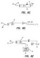
- FIGS. 6A-6Eillustrate simplified schematic diagrams of circuits that may be used in accordance with the present invention to respectively achieve the following implantable-device functions: voltage step up ( FIG. 6A ); voltage step down ( FIG. 6B ); energy reception ( FIG. 6C ); data reception ( FIG. 6D ); and data transmission ( FIG. 6E );
- FIG. 7is a simplified schematic diagram that illustrates a voltage converter circuit made in accordance with the present invention that selectively performs the five implantable-device functions illustrated in FIGS. 6A-6E ;
- FIG. 8is a table that defines the operating state of the various switches M 1 ′, M 2 , M 3 , M 4 and M 5 utilized in the circuit of FIG. 7 in order to select a desired operating mode for the circuit shown in FIG. 7 .
- the present inventionrelates to a particular type of voltage converter that may be used within an implantable medical device, such as an implantable stimulator, sensor, pump or other type of medical device providing a desired medical function.
- an implantable medical devicesuch as an implantable stimulator, sensor, pump or other type of medical device providing a desired medical function.
- the inventionwill be described below in terms of an implantable stimulator, but it is to be understood that the invention may be used within many different types of implantable devices.
- FIG. 1a block diagram of a representative implantable stimulator system 10 is illustrated.
- the system 10includes an implant device 20 , implanted under the skin 18 , coupled to an external control unit 12 through implanted coil 22 and external coil 15 .
- the external coil 15is typically carried in a housing 14 connected to the external control unit 12 via flexible cable 13 .
- An external power source 16which may be, e.g., a rechargeable or replaceable battery, provides operating power for the external control unit.
- the external power source 16may also provide operating power for the implant device 20 through the link provided through the coils 15 and 22 , either continuously or on an intermittent basis. Intermittent power is provided, e.g., such as when the implant device includes a replenishable power source, such as a rechargeable battery, and the battery is intermittently recharged.
- the implant device 20when functioning as a stimulator, includes a plurality of electrodes 24 a and 24 b connected to the implant device 20 via conductive leads or wires 23 a and 23 b , respectively.
- the electrodes 24 a and 24 bare typically implanted near body tissue or nerves 26 that are to be stimulated.
- the system 10functions as follows:
- the implant device 20 and electrodes 24 a and 24 bare implanted in the desired location under the patient's skin 18 .
- the implant coil 22is shown separate from the implant device 20 in FIG. 1 , the coil 22 is typically mounted to or housed within the same hermetically-sealed case used to house the electronic circuitry associated with the implant device 20 .
- power and/or control datae.g., programming data
- the implant device 20operates as directed by the control signals received, or as steered by the program data stored therein, to generate electrical stimulation pulses for delivery to the tissue 26 via the electrodes 24 a and 24 b.
- Some implant devices 20do not contain an implanted power source, and such devices must thus receive their operating power continuously from the external control unit.
- Other implant devices 20do contain an implanted power source, e.g., a rechargeable battery, and such devices thus receive their operating power from the implanted power source.
- implanted power sourcee.g., a rechargeable battery
- implanted power sourcereplenished, e.g., have the battery recharged.
- Such rechargingoccurs via a link with the external control unit 12 , or equivalent device, through the coils 22 and 15 .
- FIG. 2shows a sectional schematic diagram of one type of implantable microstimulator 30 within which the present invention may be used.
- the microstimulator device 30includes electrical circuitry 32 housed within a hermetically-sealed case 34 . At each end of the case 34 are electrodes 36 a and 36 b . These electrodes 36 a and 36 b are electrically connected to the electrical circuitry 32 via conductors, e.g., wires, 37 a and 37 b , respectively, and appropriate feed-through conductors 38 a and 38 b that pass through the wall of the hermetically-sealed case 34 .
- conductorse.g., wires, 37 a and 37 b
- microstimulator device 30is very small, and can typically be easily implanted at the desired implant location through the lumen of a hypodermic needle, or other cannula.
- a microstimulatoris disclosed, e.g., in U.S. Pat. No. 5,324,316, incorporated herein by reference.
- One method of making such a microstimulatoris disclosed, e.g., in U.S. Pat. No. 5,405,367, also incorporated herein by reference.
- FIG. 3a functional block diagram of a typical implantable stimulator 40 .
- the stimulator 40includes electronic circuitry that performs the following functions: an energy receiver 42 , a data receiver 44 , a power source 46 , a control circuit 48 , a voltage converter 50 , a pulse generator 52 , and a back telemetry circuit 54 .
- An implanted coil 56is connected to both the energy receiver 42 and the data receiver 44 and provides a means through which power and data signals may be received by the stimulator 40 .
- Another coil 58which in some embodiments may comprise the same, or a portion of, the coil 56 , is connected to the back telemetry circuit 54 , and provides a means through which back telemetry data may be sent to an external receiver.
- an external receivermay be included, for example, within the external control unit 12 ( FIG. 1 ). All of the above-described elements of the stimulator 40 are housed within an hermetically-sealed housing or case 60 , thereby allowing the stimulator 40 to be implanted within body tissue.
- a plurality of electrodes 62 a , 62 bExternal to the housing 60 , but still adapted to be implanted within body tissue, is a plurality of electrodes 62 a , 62 b . Electrical connection with the plurality of electrodes 62 a , 62 b is established through a plurality of wire conductors 63 a , 63 b (which may be included within a single implantable lead body, as is known in the art) which are respectively connected to a plurality of feed-through connectors 64 a , 64 b that pass through the hermetically-sealed wall of the case 60 .
- the pulse generator 52is electrically coupled to the plurality of feed-through connectors 64 a , 64 b on the inside of the case 60 .
- an RF signal(represented in FIG. 3 by the wavy arrow 66 ) is received through coil 56 .
- the RF signalcomprises a modulated carrier signal.
- the carrier signalis rectified in the energy receiver 42 and provides charging power for the power source 46 .
- the carrier signalis demodulated in the data receiver 44 and the data thus recovered provides control and/or programming data to the control circuit 48 .
- the control circuit 48typically a microprocessor, includes memory circuitry (not shown) wherein programming and/or control data may be stored. Based on this programming and/or control data, the control circuit 48 drives the pulse generator circuit 52 so that it generates and delivers electrical stimulation pulses to the patient through selected groupings of the plurality of electrodes 62 a , 62 b.
- the process of generating the electrical stimulation pulseswhich typically vary in amplitude as a function of the control and/or programming data, and in order to conserve power, it is necessary to provide a high level supply voltage to the pulse generator circuit 52 .
- a supply voltage VCprovided to the pulse generator circuit by the voltage converter 50 , must be greater than 10 volts, e.g., 12 volts or more due to losses within the pulse generation circuit.
- the voltage converter circuit 50is typically used in a stimulator 40 to step up the power source voltage VS, e.g., the battery voltage, to a level suitable for use by the pulse generator circuit 52 .
- the power source voltage VSis typically a low value, e.g., 2 or 3 volts.
- the voltage converter circuit 50is needed to boost, or step up, the source voltage VS from its relatively low value to a higher level VC as needed by the pulse generator circuit 52 .
- the capacitors used in a switched capacitor network, and/or transformersmust be employed.
- the difference between the supply voltage VC and the output voltage VOmay be referred to as the compliance voltage.
- the compliance voltageis kept as low as possible because the power dissipated in the pulse generator circuit (which is generally considered as wasted or lost power because it does not represent power delivered to the tissue) is proportional to the square of the compliance voltage.
- the compliance voltagecannot always be minimized because the current delivered through the electrodes 62 a and 62 b to the body tissue varies over a wide range; and hence the compliance voltage must also vary over a wide range.
- the voltage converter circuit 50is used to adjust the supply voltage VC, typically to provide a small number of discrete levels of supply voltage, as a function of the current to be delivered in the stimulation pulse.
- a typical voltage converter circuit 50may provide one of four different supply voltages VC to the pulse generator circuit 52 , e.g., a VC of 2.5, 5.0, 7.5 or 10 volts, as a function of the programmed amplitude of the stimulation pulse that is to be delivered to the tissue.
- An implantable stimulator having such a featureis described, e.g., in U.S. Pat. No. 5,522,865, incorporated herein by reference.
- the voltage converter circuit 50performs a very important function within the implantable stimulator 40 .
- the voltage converter circuit 50represents additional circuitry that requires bulky circuit components, which takes up needed and valuable space within the case 60 , and much of which also consumes additional power.
- most voltage converter circuits 50tend to be very inefficient. That is, a capacitor charge pump circuit, for example, typically may operate at efficiencies that may be less than 50%.
- space and power considerationsare paramount to the design of the stimulator.
- the present inventionadvantageously provides circuitry for use within an implantable stimulator device that performs the voltage conversion function using fewer and less bulky components. This frees up valuable space within the case of the stimulator that may be used for other functions (or allows the case to be smaller), and consumes less power than has heretofore been achievable. Additionally, the present invention provides a circuit that performs multiple functions, thus allowing fewer circuit components to be used within the stimulator design, thereby permitting the overall stimulator design to be smaller or more compact.
- FIG. 4a type of fly back converter circuit is illustrated that may be used to step up the voltage of a power source without the need for a switched capacitor network .
- the fly back circuit shown in FIG. 4includes an inductor or coil L 1 having one end connected to a power source 70 . The other end of the coil L 1 is connected to a first circuit node 72 .
- a switching transistor M 1is connected between the first node 72 and ground.
- the transistor M 1has a gate terminal 73 connected to a duty cycle control circuit 74 .
- node 72is effectively switched to ground potential through a very low impedance path.
- transistor M 1When transistor M 1 is turned OFF, through absence of a signal applied to its gate terminal 73 , it represents a very high impedance path, and thus effectively maintains node 72 disconnected from ground.
- diode D 1Also connected to node 72 of the fly back circuit shown in FIG. 4 is the cathode side of diode D 1 .
- the anode side of diode DIis connected to an output node 75 .
- An output capacitor C 1is connected between the output node 75 and ground.
- a load, represented in FIG. 4 by phantom resistor RL,is also connected between the output node 75 and ground.
- the duty cycle control circuit 74applies a pulsed signal to the gate of transistor M 1 , thereby effectively turning transistor M 1 ON and OFF as controlled by the pulsed signal.
- a high voltage applied to the gate of M 1may turn M 1 ON (provide a low impedance path between node 72 and ground), and a low voltage applied to the gate of M 1 may turn M 1 OFF (provide a high impedance path between node 72 and ground).
- a sequence of high and low voltagesmay be applied to the gate 73 of transistor M 1 through application of a pulsed signal 81 generated by the duty cycle control circuit 74 .
- a pulseWhen a pulse is present, the voltage is high, and the transistor M 1 is turned ON.
- the transistor M 1is turned OFF.
- the ratio of time when the pulse is high to the total cycle timeis known as the “duty cycle”.
- the duty cycleis defined as shown in FIG. 5 .
- a pulsed signal 81comprises a train of pulses 80 .
- Each pulse 80comprises a high voltage for a period of time T 2 and a low voltage for a period of time T 3 .
- the total cycle time T 1is equal to T 2 plus T 3 .
- the magnitude of the output voltage VOUT and output current IOmay advantageously be controlled by adjusting the duty cycle of the signal 81 .
- a higher duty cyclecauses both VOUT and IO to increase, whereas a lower duty cycle causes VOUT and IO to decrease.
- the duty cycle control circuit 74may also be referred to as a pulse width modulator circuit.
- a sensing circuit 76 Amay be used to monitor the output voltage VOUT, and to compare the sensed output voltage to either a reference voltage VREF and/or a programmed reference signal PROG (which typically is presented to the sensing circuit 76 A as a digital signal).
- the sensing circuit 76 Agenerates a difference signal, on signal line 76 C, representing the difference between the sensed output voltage VOUT and the reference voltage VREF and/or PROG.
- This difference signalcontrols a gate control circuit 76 B, which modulates the gate of transistor M 1 so as to drive the difference signal to zero.
- FIGS. 6A-6Eadditional simplified schematic diagrams of circuits are illustrated that may be used in accordance with the present invention to achieve desired functions. More particularly, a voltage step up function may be achieved using the circuit shown in FIG. 6A ; a voltage step down function may be achieved using the circuit of FIG. 6B ; an energy reception function may be achieved using the circuit of FIG. 6C ; a data reception function may be achieved using the circuit of FIG. 6D ; and a data transmission function may be achieved using the circuit of FIG. 6E .
- many of the components used in the circuits of FIGS. 6A-6Emay be the same. Common reference numerals are used to denote the components that may be the same. A brief explanation of each of these functions will next be described.
- FIG. 6Adepicts a circuit that performs a voltage step up function. This circuit is substantially the same as the circuit previously described in connection with FIG. 4 , except that the load resistance RL is not shown. However, it is to be understood that a load resistance may be present. It should also be understood that whereas FIG. 4 shows a duty cycle control circuit 74 controlling switch M 1 , FIG. 6A shows a PWM (pulse width modulation) control circuit 74 ′ controlling switch M 1 . These circuits perform the same function (turning switch M 1 ON or OFF) and, for purposes of the present invention, are substantially the same.
- FIG. 6Bdepicts a circuit that performs a voltage step down function.
- a coil L 1is connected between circuit nodes 75 and 76 .
- Node 75represents the output node of the circuit whereon the output voltage VOUT is present.
- Capacitor C 1is connected between node 75 and ground.
- the anode side of a diode D 2is connected to node 76 , while the cathode side of diode D 2 is connected to ground.
- One leg of a transistor switch M 2is connected to node 76 , while the other leg of transistor switch M 2 is connected to the power source 70 at node 77 .
- a gate terminal 78 of transistor M 2is connected to pulse-width modulation (PWM) control circuit 74 ′′.
- PWMpulse-width modulation
- FIG. 6Cshows a circuit that receives energy from an external source.
- the energy receive circuit shown in FIG. 6Cincludes a coil L 1 having a capacitor C 1 connected in parallel with the coil L 1 , with one side of the parallel connection being grounded.
- the coil L 1 and capacitor C 1comprise an “LC” circuit that is tuned to the frequency of an incoming RF signal 83 (represented in FIG. 6C by a wavy arrow).
- Diode D 1is connected between output node 75 and the other side of the L 1 -C 2 parallel connection, with the cathode of D 1 being connected to node 75 .
- Capacitor C 1is connected between output node 75 and ground.
- the circuit shown in FIG. 6Creceives the incoming RF signal 83 through coil L 1 , tuned to the frequency of the signal 83 by capacitor C 2 .
- Diode D 1rectifies the signal, storing the positive half cycles of the received signal 83 on capacitor C 1 .
- the voltage thus developed on capacitor C 1functions as an output voltage VOUT for use within the implant device.
- Such data receiver circuitincludes coil L 1 connected in parallel with variable capacitor C 3 .
- a modulated RF signal 88 ′is received through the coil L 1 .
- the value of C 3is adjusted, as required, so that the L 1 -C 3 circuit is tuned to the frequency of modulation applied to the incoming RF signal 88 ′.
- Node 72 ′which represents an output node of the L 1 -C 3 circuit, is connected to the input of an amplifier U 1 .
- the output signal provided by the amplifier U 1comprises a Data Out signal that reflects the modulation applied to the incoming modulated RF signal 88 ′.
- the data transmitter circuitincludes a coil L 1 connected in parallel with an adjustable variable capacitor C 3 .
- One side of the L 1 -C 3 parallel connectionis connected to a power source 70 .
- the other side of the L 1 -C 3 parallel connectionidentified as node 72 ′ in FIG. 6E , is connected to the anode of diode D 3 .
- the cathode of diode D 3is connected through a switch transistor M 3 to ground.
- the gate terminal of switch M 3is driven by a “Data Mod” (data modulation) signal.
- Data Moddata modulation
- FIGS. 6A-6Eprovide the functions of voltage step up ( FIG. 6A ), voltage step down ( FIG. 6B ), energy reception ( FIG. 6C ), data reception ( FIG. 6D ), and data transmission ( FIG. 6E ). All of these functions are typically required within an implantable stimulator device ( FIG. 3 ).
- the present inventionadvantageously combines all the functions performed by the individual circuits shown in FIGS. 6A-6E into one circuit as shown in FIG. 7 .
- Such combined circuitmay be referred to as a “voltage converter using an RF-powering coil”, and is particularly suited for use within an implantable medical device, such as an implantable neural stimulator.
- the combined circuit provided by the present inventionuses an RF-powering coil in combination with other circuit elements to perform the function of receiving RF power from an external source.
- the received RF powermay be modulated in order to transmit control data into the circuit.
- such RF-powering coilmay be used to help transmit data out of the circuit.
- the RF-coil used to receive power, data, and to transmit datamay also be used to selectively convert the received power (i.e., voltage) up or down in order to make operation of the circuit more efficient.
- the circuit of FIG. 7(i.e., the voltage converter circuit using an RF-powering coil provided by the present invention) includes a receiving/transmitting coil L 1 ′.
- the coil L 1 ′includes ends attached to circuit nodes 72 ′ and 85 , respectively.
- Node 85is connected through transistor switch M 1 ′ to source voltage VS.
- the coil L 1 ′further includes a tap point 85 ′, where there are N 2 turns of the coil between tap point 85 ′ and node 85 , and N 1 turns between tap point 85 ′ and node 72 ′.
- N 1are 10 to 100 turns, and for N 2 are also 10 to 100 turns, and wherein the inductance of coil L 1 ′ is between about 10 to 100 microhenries ( ⁇ H).
- N 1 and N 2may vary from 1 to 1000 turns, and L 1 ′ may vary between 1 to 1000 ⁇ H.
- a series combination of a capacitor C 3 ′ and transistor switch M 4is connected between circuit node 72 ′ and tap point 85 ′.
- Another transistor switch M 5connects the tap point 85 ′ of coil L 1 ′ to ground (node 87 ).
- Yet another transistor switch M 2connects the tap point 85 ′ to the source voltage VS.
- the cathode end of a diode D 2is also connected to the tap point 85 ′ of the coil L 1 ′; while the anode end of diode D 2 is connected to ground.
- the cathode end of another diode D 3is connected to node 72 ′.
- the anode end of diode D 3is connected through transistor switch M 3 to ground (node 87 ).
- the anode end of diode D 3is also connected to the input of signal amplifier U 1 .
- the cathode end of yet another diode D 1is also connected to node 72 ′.
- the anode end of diode D 1is connected to circuit node 75 ′.
- a capacitor C 1is connected between node 75 ′ and ground (node 87 ).
- Circuit node 75 ′is the location where the output voltage VOUT is made available when the circuit operates in a voltage step up or step down mode. If needed, a suitable voltage clamp circuit 91 may be connected between node 75 ′ and ground in order to prevent the voltage at the output node 75 ′ from exceeding some predetermined value.
- the circuit of FIG. 7includes five transistor switches, M 1 ′, M 2 , M 3 , M 4 and M 5 .
- the state of these five switchesdetermines which circuit function is performed as defined in the table presented in FIG. 8 . That is, as seen in FIG. 8 , in order for the circuit of FIG. 7 to operate in a voltage step up mode, switch M 1 ′ is turned ON, M 2 is turned OFF, M 3 is modulated with a PWM signal from a suitable duty cycle control circuit (see FIGS. 4 and 5 ), and both M 4 and M 5 are turned OFF. Under these conditions, the circuit of FIG. 7 effectively reduces to the circuit shown in FIG.
- the level of the output voltage VOUTis determined in large part by the duty cycle of the signal applied to the gate of transistor switch M 3 , as explained previously.
- switch M 1 ′is turned OFF, switch M 2 is modulated with a PWM signal from a suitable duty cycle control circuit 74 ′′ ( FIG. 6B ), and switches M 3 , M 4 and M 5 are all turned OFF.
- the circuit of FIG. 7effectively reduces to the circuit shown in FIG. 6B , with the only difference being diode D 1 connected between nodes 72 ′ and 75 ′ (which diode does not significantly alter the circuit's operation), and only a portion of coil L 1 ′ being used (i.e., only the turns N 1 are used).
- the circuitperforms a voltage step down function, as described previously in connection with FIG. 6B .
- the circuit of FIG. 7may also selectively operate in an energy receive mode and a data receive mode by turning switches M 1 ′, M 2 and M 3 OFF, and by turning switches M 4 and M 5 ON. With the switches in these positions, the circuit of FIG. 7 effectively reduces to the circuit shown in FIG. 6C , and to the circuit shown in FIG. 6D , with the only difference being that just a portion (N 1 turns) of the coil L 1 ′ is used as part of the circuit. In this configuration and mode, the circuit of FIG. 7 thus performs both an energy receive function as described previously in connection with FIG. 6C , and a data receive function as described previously in connection with FIG. 6D .
- the circuit of FIG. 7may also selectively operate in a data transmit mode by turning switch M 2 OFF, by modulating switch M 3 with a data signal, and by turning switch M 1 ′ ON.
- Switch M 4may be either OFF or ON depending upon whether capacitor C 3 ′ is deemed necessary to better tune coil L 1 ′ for efficient data transmission. For many data transmissions, capacitor C 3 ′ should not be needed. Under these conditions, the circuit of FIG. 7 effectively reduces to the circuit shown in FIG. 6E . Hence, in such configuration and mode, the circuit performs a data transmit function, as described previously in connection with FIG. 6E .
- the circuit of FIG. 7may operate in any one of five different modes. Some of these modes, e.g., the energy receive mode and the data receive mode, may operate simultaneously. Others of the modes may be invoked in a time-multiplexed manner, e.g., with a first mode being followed by a second mode, and with the second mode being followed by a third mode, as required, depending upon the particular application at hand.
- an energy and data receive modemay operate as a first mode to allow the device to receive operating power (e.g, to recharge a battery) and/or to receive initial programming control signals.
- This first modemay then be followed by a second mode, e.g., a voltage step up mode, initiated by changing the state of switches M 1 ′, M 2 , M 3 , M 4 and M 5 as defined in FIG. 8 , during which the voltage of the primary power source is stepped up to a voltage needed by the device in order for it to perform its intended function.
- a third modee.g., a data transmit mode, may be invoked in order to allow the implant device to transmit data to an external receiver.
- the component values of the componentsi.e., the transistor switches and capacitors and coil, used in the circuit of FIG. 7 may be readily ascertained by those of skill in the art for a particular application and desired RF frequency.
- the invention described hereinprovides a voltage converter circuit for use within an implantable device, e.g., such as an implantable microstimulator or similar type of neural stimulator, that is compact, efficient, and provides a wide range of output voltages and currents.
- the inventionprovides a voltage converter circuit that avoids the use of a network of capacitors switched between parallel and series, or other, configurations in order to provide the step up and step down voltage conversion function.
Landscapes
- Health & Medical Sciences (AREA)
- Engineering & Computer Science (AREA)
- Biomedical Technology (AREA)
- Nuclear Medicine, Radiotherapy & Molecular Imaging (AREA)
- Radiology & Medical Imaging (AREA)
- Life Sciences & Earth Sciences (AREA)
- Animal Behavior & Ethology (AREA)
- General Health & Medical Sciences (AREA)
- Public Health (AREA)
- Veterinary Medicine (AREA)
- Electrotherapy Devices (AREA)
Abstract
Description
Claims (12)
Priority Applications (5)
| Application Number | Priority Date | Filing Date | Title |
|---|---|---|---|
| US12/099,474US7904171B2 (en) | 2000-03-17 | 2008-04-08 | Voltage converter for implantable microstimulator using RF-powering coil |
| US12/623,758US8155752B2 (en) | 2000-03-17 | 2009-11-23 | Implantable medical device with single coil for charging and communicating |
| US13/420,830US8781596B2 (en) | 2000-03-17 | 2012-03-15 | Implantable medical device with single coil for charging and communicating |
| US14/327,065US9155898B2 (en) | 2000-03-17 | 2014-07-09 | Implantable medical device with multi-function single coil |
| US14/880,011US9446250B2 (en) | 2000-03-17 | 2015-10-09 | Implantable medical device with multi-function single coil |
Applications Claiming Priority (5)
| Application Number | Priority Date | Filing Date | Title |
|---|---|---|---|
| US18999200P | 2000-03-17 | 2000-03-17 | |
| US09/799,467US6631296B1 (en) | 2000-03-17 | 2001-03-05 | Voltage converter for implantable microstimulator using RF-powering coil |
| US10/679,621US6856838B2 (en) | 2000-03-17 | 2003-10-06 | Voltage converter for implantable microstimulator using RF-powering coil |
| US11/047,052US7379775B2 (en) | 2000-03-17 | 2005-01-31 | Voltage converter for implantable microstimulator using RF-powering coil |
| US12/099,474US7904171B2 (en) | 2000-03-17 | 2008-04-08 | Voltage converter for implantable microstimulator using RF-powering coil |
Related Parent Applications (1)
| Application Number | Title | Priority Date | Filing Date |
|---|---|---|---|
| US11/047,052DivisionUS7379775B2 (en) | 2000-03-17 | 2005-01-31 | Voltage converter for implantable microstimulator using RF-powering coil |
Related Child Applications (1)
| Application Number | Title | Priority Date | Filing Date |
|---|---|---|---|
| US12/623,758Continuation-In-PartUS8155752B2 (en) | 2000-03-17 | 2009-11-23 | Implantable medical device with single coil for charging and communicating |
Publications (2)
| Publication Number | Publication Date |
|---|---|
| US20080208293A1 US20080208293A1 (en) | 2008-08-28 |
| US7904171B2true US7904171B2 (en) | 2011-03-08 |
Family
ID=28677966
Family Applications (4)
| Application Number | Title | Priority Date | Filing Date |
|---|---|---|---|
| US09/799,467Expired - LifetimeUS6631296B1 (en) | 2000-03-17 | 2001-03-05 | Voltage converter for implantable microstimulator using RF-powering coil |
| US10/679,621Expired - LifetimeUS6856838B2 (en) | 2000-03-17 | 2003-10-06 | Voltage converter for implantable microstimulator using RF-powering coil |
| US11/047,052Expired - LifetimeUS7379775B2 (en) | 2000-03-17 | 2005-01-31 | Voltage converter for implantable microstimulator using RF-powering coil |
| US12/099,474Expired - Fee RelatedUS7904171B2 (en) | 2000-03-17 | 2008-04-08 | Voltage converter for implantable microstimulator using RF-powering coil |
Family Applications Before (3)
| Application Number | Title | Priority Date | Filing Date |
|---|---|---|---|
| US09/799,467Expired - LifetimeUS6631296B1 (en) | 2000-03-17 | 2001-03-05 | Voltage converter for implantable microstimulator using RF-powering coil |
| US10/679,621Expired - LifetimeUS6856838B2 (en) | 2000-03-17 | 2003-10-06 | Voltage converter for implantable microstimulator using RF-powering coil |
| US11/047,052Expired - LifetimeUS7379775B2 (en) | 2000-03-17 | 2005-01-31 | Voltage converter for implantable microstimulator using RF-powering coil |
Country Status (1)
| Country | Link |
|---|---|
| US (4) | US6631296B1 (en) |
Cited By (8)
| Publication number | Priority date | Publication date | Assignee | Title |
|---|---|---|---|---|
| US20100315039A1 (en)* | 2009-06-15 | 2010-12-16 | Kyozo Terao | Device housing a battery and charging pad |
| WO2019140404A1 (en)* | 2018-01-14 | 2019-07-18 | Stimaire, Inc. | Wireless neural stimulator with injectable |
| US11116975B2 (en) | 2015-11-09 | 2021-09-14 | Bluewind Medical Ltd. | Optimization of application of current |
| US11213685B2 (en) | 2017-06-13 | 2022-01-04 | Bluewind Medical Ltd. | Antenna configuration |
| US11278719B2 (en) | 2012-12-06 | 2022-03-22 | Bluewind Medical Ltd. | Delivery of implantable neurostimulators |
| US11400299B1 (en) | 2021-09-14 | 2022-08-02 | Rainbow Medical Ltd. | Flexible antenna for stimulator |
| US11439833B2 (en) | 2016-11-23 | 2022-09-13 | Bluewind Medical Ltd. | Implant-delivery tool |
| US11648410B2 (en) | 2012-01-26 | 2023-05-16 | Bluewind Medical Ltd. | Wireless neurostimulators |
Families Citing this family (109)
| Publication number | Priority date | Publication date | Assignee | Title |
|---|---|---|---|---|
| US7136699B2 (en)* | 2002-10-02 | 2006-11-14 | Standen, Ltd. | Apparatus for destroying dividing cells |
| US8155752B2 (en)* | 2000-03-17 | 2012-04-10 | Boston Scientific Neuromodulation Corporation | Implantable medical device with single coil for charging and communicating |
| US6631296B1 (en) | 2000-03-17 | 2003-10-07 | Advanced Bionics Corporation | Voltage converter for implantable microstimulator using RF-powering coil |
| US7209792B1 (en) | 2001-05-24 | 2007-04-24 | Advanced Bionics Corporation | RF-energy modulation system through dynamic coil detuning |
| US6985773B2 (en) | 2002-02-07 | 2006-01-10 | Cardiac Pacemakers, Inc. | Methods and apparatuses for implantable medical device telemetry power management |
| ES2426255T3 (en)* | 2002-06-28 | 2013-10-22 | Boston Scientific Neuromodulation Corporation | Microstimulator that has a built-in power source and a two-way telemetry system |
| US7428438B2 (en)* | 2002-06-28 | 2008-09-23 | Boston Scientific Neuromodulation Corporation | Systems and methods for providing power to a battery in an implantable stimulator |
| US7822480B2 (en) | 2002-06-28 | 2010-10-26 | Boston Scientific Neuromodulation Corporation | Systems and methods for communicating with an implantable stimulator |
| US7027860B2 (en)* | 2002-08-29 | 2006-04-11 | Department Of Veterans Affairs | Microstimulator neural prosthesis |
| US7615010B1 (en)* | 2002-10-03 | 2009-11-10 | Integrated Sensing Systems, Inc. | System for monitoring the physiologic parameters of patients with congestive heart failure |
| AU2002953278A0 (en)* | 2002-12-12 | 2003-01-02 | Skop Australia Pty Ltd | Electro stimulation treatment apparatus and method |
| US7203549B2 (en) | 2003-10-02 | 2007-04-10 | Medtronic, Inc. | Medical device programmer with internal antenna and display |
| US7991479B2 (en) | 2003-10-02 | 2011-08-02 | Medtronic, Inc. | Neurostimulator programmer with clothing attachable antenna |
| US7561921B2 (en) | 2003-10-02 | 2009-07-14 | Medtronic, Inc. | Neurostimulator programmer with internal antenna |
| US7272445B2 (en) | 2003-10-02 | 2007-09-18 | Medtronic, Inc. | Medical device programmer with faceplate |
| US7356369B2 (en)* | 2003-10-02 | 2008-04-08 | Medtronic, Inc. | Z-axis assembly of medical device programmer |
| US7729766B2 (en) | 2003-10-02 | 2010-06-01 | Medtronic, Inc. | Circuit board construction for handheld programmer |
| US7263406B2 (en) | 2003-10-02 | 2007-08-28 | Medtronic, Inc. | Medical device programmer with selective disablement of display during telemetry |
| US8442643B2 (en)* | 2003-10-02 | 2013-05-14 | Medtronic, Inc. | Medical device programmer with reduced-noise power supply |
| WO2005099817A1 (en) | 2004-04-07 | 2005-10-27 | Cardiac Pacemakers, Inc. | Rf wake-up of implantable medical device |
| US8176922B2 (en)* | 2004-06-29 | 2012-05-15 | Depuy Products, Inc. | System and method for bidirectional communication with an implantable medical device using an implant component as an antenna |
| US8428712B2 (en)* | 2004-07-20 | 2013-04-23 | Medtronic, Inc. | Concurrent delivery of treatment therapy with telemetry in an implantable medical device |
| US7720546B2 (en)* | 2004-09-30 | 2010-05-18 | Codman Neuro Sciences Sárl | Dual power supply switching circuitry for use in a closed system |
| US7384403B2 (en)* | 2004-12-17 | 2008-06-10 | Depuy Products, Inc. | Wireless communication system for transmitting information from a medical device |
| WO2006069144A2 (en)* | 2004-12-21 | 2006-06-29 | University Of Pittsburgh - Of The Commonwealth System Of Higher Education | Deep brain stimulation apparatus, and associated methods |
| US8001975B2 (en) | 2004-12-29 | 2011-08-23 | Depuy Products, Inc. | Medical device communications network |
| US7218969B2 (en)* | 2005-01-19 | 2007-05-15 | Cardiac Pacemakers, Inc. | Dynamic channel selection for RF telemetry with implantable device |
| US7664553B2 (en) | 2005-04-27 | 2010-02-16 | Cardiac Pacemakers, Inc. | System and method for enabling communications with implantable medical devices |
| US8193745B2 (en)* | 2005-05-13 | 2012-06-05 | Schlumberger Technology Corporation | Filtering and boosting a signal from a drive circuit |
| US7200504B1 (en) | 2005-05-16 | 2007-04-03 | Advanced Bionics Corporation | Measuring temperature change in an electronic biomedical implant |
| US7957805B2 (en)* | 2005-06-01 | 2011-06-07 | Boston Scientific Neuromodulation Corporation | Implantable microstimulator with external electrodes disposed on a film substrate and methods of manufacture and use |
| US8862243B2 (en) | 2005-07-25 | 2014-10-14 | Rainbow Medical Ltd. | Electrical stimulation of blood vessels |
| JP4498242B2 (en)* | 2005-08-04 | 2010-07-07 | セイコーインスツル株式会社 | Electronics |
| WO2007019491A2 (en)* | 2005-08-08 | 2007-02-15 | Katims Jefferson J | Method and apparatus for producing therapeutic and diagnostic stimulation |
| US7801620B2 (en)* | 2005-08-29 | 2010-09-21 | Cardiac Pacemakers, Inc. | RF telemetry link quality assessment system and method |
| US8027727B2 (en)* | 2005-08-29 | 2011-09-27 | Cardiac Pacemakers, Inc. | Pacemaker RF telemetry repeater and method |
| US8175717B2 (en)* | 2005-09-06 | 2012-05-08 | Boston Scientific Neuromodulation Corporation | Ultracapacitor powered implantable pulse generator with dedicated power supply |
| US7890181B2 (en)* | 2005-09-12 | 2011-02-15 | Medtronic, Inc. | System and method for unscheduled wireless communication with a medical device |
| US8065018B2 (en) | 2005-09-12 | 2011-11-22 | Medtronic, Inc. | System and method for unscheduled wireless communication with a medical device |
| US8380320B2 (en)* | 2005-09-12 | 2013-02-19 | Medtronic, Inc. | Implantable medical device communication system with macro and micro sampling intervals |
| US8185210B2 (en)* | 2005-09-12 | 2012-05-22 | Medtronic, Inc. | Communication system and method with preamble encoding for an implantable medical device |
| US8160704B2 (en)* | 2005-11-02 | 2012-04-17 | Cardiac Pacemakers, Inc. | System and method for enabling relayed communications by implantable medical devices |
| US7872884B2 (en)* | 2005-11-03 | 2011-01-18 | Boston Scientific Neuromodulation Corporation | Cascaded step-up converter and charge pump for efficient compliance voltage generation in an implantable stimulator device |
| US7686768B2 (en) | 2005-11-23 | 2010-03-30 | Vital Sensors Holding Company, Inc. | Implantable pressure monitor |
| US7682313B2 (en)* | 2005-11-23 | 2010-03-23 | Vital Sensors Holding Company, Inc. | Implantable pressure monitor |
| US7729758B2 (en) | 2005-11-30 | 2010-06-01 | Boston Scientific Neuromodulation Corporation | Magnetically coupled microstimulators |
| US20070142872A1 (en)* | 2005-12-21 | 2007-06-21 | Mickle Marlin H | Deep brain stimulation apparatus, and associated methods |
| US7657310B2 (en) | 2006-01-26 | 2010-02-02 | Cyberonics, Inc. | Treatment of reproductive endocrine disorders by vagus nerve stimulation |
| WO2007106692A2 (en)* | 2006-03-15 | 2007-09-20 | University Of Pittsbugh Of The Commonwealth System Of Higher Education | Vagus nerve stimulation apparatus, and associated methods |
| US8185204B2 (en)* | 2006-07-12 | 2012-05-22 | Cardiac Pacemakers, Inc. | Implantable medical device telemetry with adaptive frequency hopping |
| US7623922B2 (en)* | 2006-07-12 | 2009-11-24 | Cardiac Pacemakers, Inc. | Implantable medical device telemetry with periodic frequency hopping |
| US20080077184A1 (en)* | 2006-09-27 | 2008-03-27 | Stephen Denker | Intravascular Stimulation System With Wireless Power Supply |
| US7881803B2 (en) | 2006-10-18 | 2011-02-01 | Boston Scientific Neuromodulation Corporation | Multi-electrode implantable stimulator device with a single current path decoupling capacitor |
| US8660660B2 (en)* | 2006-11-14 | 2014-02-25 | Second Sight Medical Products, Inc. | Power scheme for implant stimulators on the human or animal body |
| US7991483B1 (en) | 2006-12-21 | 2011-08-02 | Boston Scientific Neuromodulation Corporation | Implantable electrodes containing polyoxometalate anions and methods of manufacture and use |
| US8046079B2 (en) | 2007-03-13 | 2011-10-25 | Cardiac Pacemakers, Inc. | Implantable medical device telemetry with hop-on-error frequency hopping |
| WO2008137452A1 (en)* | 2007-05-04 | 2008-11-13 | Kenergy Royalty Company, Llc | Implantable high efficiency digital stimulation device |
| US20120123508A1 (en)* | 2010-11-12 | 2012-05-17 | Massachusetts Institute Of Technology | Methods and apparatus for wireless control of biological tissue |
| US20080312719A1 (en)* | 2007-06-13 | 2008-12-18 | Cardiometrix, Inc. | Transducer wireless control system and method |
| US8080064B2 (en) | 2007-06-29 | 2011-12-20 | Depuy Products, Inc. | Tibial tray assembly having a wireless communication device |
| US8131377B2 (en)* | 2007-07-11 | 2012-03-06 | Boston Scientific Neuromodulation Corporation | Telemetry listening window management for an implantable medical device |
| CA2739852C (en)* | 2007-10-16 | 2022-11-29 | Peter Forsell | A method and apparatus for supplying energy to a medical device |
| US9005106B2 (en) | 2008-01-31 | 2015-04-14 | Enopace Biomedical Ltd | Intra-aortic electrical counterpulsation |
| US8538535B2 (en) | 2010-08-05 | 2013-09-17 | Rainbow Medical Ltd. | Enhancing perfusion by contraction |
| JP2009273327A (en)* | 2008-05-10 | 2009-11-19 | Sanyo Electric Co Ltd | Battery built-in apparatus and charging cradle |
| US8494640B2 (en) | 2008-07-28 | 2013-07-23 | Boston Scientific Neuromodulation Corporation | System and method for increasing relative intensity between cathodes and anodes of neurostimulation system |
| CN101656506A (en)* | 2008-08-20 | 2010-02-24 | 鸿富锦精密工业(深圳)有限公司 | Motor driving system |
| JP5587892B2 (en)* | 2008-10-28 | 2014-09-10 | コーニンクレッカ フィリップス エヌ ヴェ | Further use of screw threads |
| US20100164688A1 (en)* | 2008-12-31 | 2010-07-01 | Texas Instruments Incorporated | Auxiliary device for implantable units |
| US9700712B2 (en) | 2009-01-26 | 2017-07-11 | Arizona Board Of Regents, A Body Corporate Of The State Of Arizona Acting For And On Behalf Of Arizona State University | Dipolar antenna system and related methods |
| WO2010135634A2 (en)* | 2009-05-22 | 2010-11-25 | Arizona Board Of Regents For And On Behalf Of Arizona State University | Systems, and methods for neurostimulation and neurotelemetry using semiconductor diode systems |
| US9233254B2 (en)* | 2009-02-17 | 2016-01-12 | Boston Scientific Neuromodulation Corporation | Selectable boost converter and charge pump for compliance voltage generation in an implantable stimulator device |
| US8577474B2 (en) | 2009-11-11 | 2013-11-05 | Boston Scientific Neuromodulation Corporation | Minimizing interference between charging and telemetry coils in an implantable medical device |
| US8457756B2 (en)* | 2009-11-11 | 2013-06-04 | Boston Scientific Neuromodulation Corporation | Using the case of an implantable medical device to broaden communication bandwidth |
| US8463392B2 (en) | 2009-11-11 | 2013-06-11 | Boston Scientific Neuromodulation Corporation | External controller/charger system for an implantable medical device capable of automatically providing data telemetry through a charging coil during a charging session |
| WO2011097289A1 (en)* | 2010-02-03 | 2011-08-11 | Medtronic, Inc. | Implantable medical devices and systems having dual frequency inductive telemetry and recharge |
| US9042995B2 (en)* | 2010-02-03 | 2015-05-26 | Medtronic, Inc. | Implantable medical devices and systems having power management for recharge sessions |
| US9107684B2 (en)* | 2010-03-05 | 2015-08-18 | Covidien Lp | System and method for transferring power to intrabody instruments |
| CN102206996A (en)* | 2010-03-31 | 2011-10-05 | 西安思坦仪器股份有限公司 | Weak signal detector |
| WO2011137168A1 (en)* | 2010-04-28 | 2011-11-03 | Medtronic, Inc. | Medical device with self-adjusting power supply |
| US8594806B2 (en) | 2010-04-30 | 2013-11-26 | Cyberonics, Inc. | Recharging and communication lead for an implantable device |
| US8808283B2 (en)* | 2010-06-30 | 2014-08-19 | Covidien Lp | Inductive powered surgical device with wireless control |
| WO2012087819A2 (en) | 2010-12-20 | 2012-06-28 | Abiomed, Inc. | Transcutaneous energy transfer system with vibration inducing warning circuitry |
| JP2014502528A (en) | 2010-12-20 | 2014-02-03 | アビオメド インコーポレイティド | Method and apparatus for accurately tracking charge available in a transdermal energy transmission system |
| DK2654878T3 (en) | 2010-12-20 | 2019-07-22 | Abiomed Inc | TRANSCUTANT ENERGY TRANSFER SYSTEM WITH A MULTIPLE OF SECONDARY COILS |
| US10286217B2 (en) | 2011-01-28 | 2019-05-14 | Medtronic, Inc. | Far field telemetry communication with a medical device during a recharge session where a prior pairing with the medical device may not exist |
| US8712541B2 (en) | 2011-01-28 | 2014-04-29 | Medtronic, Inc. | Far field telemetry operations between an external device and an implantable medical device during recharge of the implantable medical device via a proximity coupling |
| US8634927B2 (en) | 2011-01-28 | 2014-01-21 | Medtronic, Inc. | Medical device recharge systems using a controller in wireless communication with a separate recharge device |
| EP2697890B1 (en) | 2011-04-14 | 2019-02-20 | Abiomed, Inc. | Transcutaneous energy transfer coil with integrated radio frequency antenna |
| US9136728B2 (en) | 2011-04-28 | 2015-09-15 | Medtronic, Inc. | Implantable medical devices and systems having inductive telemetry and recharge on a single coil |
| US8855783B2 (en) | 2011-09-09 | 2014-10-07 | Enopace Biomedical Ltd. | Detector-based arterial stimulation |
| US9526637B2 (en) | 2011-09-09 | 2016-12-27 | Enopace Biomedical Ltd. | Wireless endovascular stent-based electrodes |
| US9002468B2 (en) | 2011-12-16 | 2015-04-07 | Abiomed, Inc. | Automatic power regulation for transcutaneous energy transfer charging system |
| TWI472354B (en)* | 2011-12-30 | 2015-02-11 | Univ Nat Chiao Tung | Current stimulator |
| US9343923B2 (en) | 2012-08-23 | 2016-05-17 | Cyberonics, Inc. | Implantable medical device with backscatter signal based communication |
| US9935498B2 (en) | 2012-09-25 | 2018-04-03 | Cyberonics, Inc. | Communication efficiency with an implantable medical device using a circulator and a backscatter signal |
| US9795788B2 (en)* | 2013-05-30 | 2017-10-24 | Pacesetter, Inc. | Implantable medical devices, and methods of use therewith, that use a same coil for receiving both communication and power signals |
| CN105899166B (en) | 2013-11-06 | 2018-07-06 | 伊诺佩斯生医有限公司 | Wireless Intravascular Stent-Based Electrodes |
| WO2015142842A2 (en) | 2014-03-17 | 2015-09-24 | Towe Bruce C | Methods and systems for measuring tissue impedance and monitoring pvd treatment using neuro-implants with improved ultrasound powering |
| WO2015187607A1 (en)* | 2014-06-02 | 2015-12-10 | The Johns Hopkins University | Harmonic excitation of mr signal for interventional mri |
| WO2017091828A1 (en)* | 2015-11-29 | 2017-06-01 | The Regents Of The University Of California | Disposable gastrointestinal implantable stimulator |
| CA3040164A1 (en)* | 2016-10-16 | 2018-04-19 | Stimaire, Inc. | Wireless neural stimulator with injectable |
| EP4233999A3 (en) | 2016-12-12 | 2023-11-22 | The Regents of The University of California | Implantable and non-invasive stimulators for gastrointestinal therapeutics |
| TR201718704A2 (en)* | 2017-11-24 | 2017-12-21 | T C Istanbul Aydin Ueniversitesi | MAKING A TENSION SENSOR AND REGULATORY AORTIC STENT FOR HYPERTENSION TREATMENT |
| HUE066899T2 (en)* | 2018-08-31 | 2024-09-28 | Hoffmann La Roche | Modular implantable medical device |
| EP3993867B1 (en) | 2019-09-06 | 2024-10-30 | Boston Scientific Neuromodulation Corporation | Management of compliance voltage for a stimulator device |
| KR102766551B1 (en) | 2020-09-09 | 2025-02-12 | 삼성전자주식회사 | Apparatus and method for relaying power wirelessly |
| CN114363132A (en) | 2020-10-13 | 2022-04-15 | 三星电子株式会社 | communication method |
| CN117595882B (en)* | 2024-01-19 | 2024-07-02 | 景昱医疗科技(苏州)股份有限公司 | Signal acquisition circuit, contact combination method, stimulator and implantable medical system |
Citations (21)
| Publication number | Priority date | Publication date | Assignee | Title |
|---|---|---|---|---|
| US3229684A (en) | 1959-12-24 | 1966-01-18 | Univ Tokyo | Telemetering system for physiological measurements |
| US3758865A (en) | 1972-01-18 | 1973-09-11 | Gen Motors Corp | Bias voltage generator for the voltage-responsive tuning elements in an electronically tuned radio receiver |
| US3796221A (en) | 1971-07-07 | 1974-03-12 | N Hagfors | Apparatus for delivering electrical stimulation energy to body-implanted apparatus with signal-receiving means |
| US4197850A (en) | 1978-11-03 | 1980-04-15 | Pacesetter Systems, Inc. | Implantable human tissue stimulator with memory protect means |
| US4345604A (en) | 1976-01-22 | 1982-08-24 | Vitafin N.V. | Long life cardiac pacer with switching power |
| US4679560A (en) | 1985-04-02 | 1987-07-14 | Board Of Trustees Of The Leland Stanford Junior University | Wide band inductive transdermal power and data link |
| US5324315A (en) | 1993-08-12 | 1994-06-28 | Medtronic, Inc. | Closed-loop downlink telemetry and method for implantable medical device |
| US5324316A (en) | 1991-12-18 | 1994-06-28 | Alfred E. Mann Foundation For Scientific Research | Implantable microstimulator |
| US5405367A (en) | 1991-12-18 | 1995-04-11 | Alfred E. Mann Foundation For Scientific Research | Structure and method of manufacture of an implantable microstimulator |
| US5522865A (en) | 1989-09-22 | 1996-06-04 | Alfred E. Mann Foundation For Scientific Research | Voltage/current control system for a human tissue stimulator |
| US5630836A (en) | 1995-01-19 | 1997-05-20 | Vascor, Inc. | Transcutaneous energy and information transmission apparatus |
| US5658319A (en)* | 1993-12-13 | 1997-08-19 | Angeion Corporation | Implantable cardioverter defibrillator having a high voltage capacitor |
| US5674264A (en) | 1995-12-01 | 1997-10-07 | Cochlear Ltd. | Feedback system to control electrode voltages in a cochlear stimulator and the like |
| US5733313A (en) | 1996-08-01 | 1998-03-31 | Exonix Corporation | RF coupled, implantable medical device with rechargeable back-up power source |
| US5741316A (en) | 1996-12-02 | 1998-04-21 | Light Sciences Limited Partnership | Electromagnetic coil configurations for power transmission through tissue |
| US5769877A (en) | 1995-01-04 | 1998-06-23 | Plexus, Inc. | High value capacitive, replenishable power source |
| US5814089A (en) | 1996-12-18 | 1998-09-29 | Medtronic, Inc. | Leadless multisite implantable stimulus and diagnostic system |
| US5991664A (en) | 1997-03-09 | 1999-11-23 | Cochlear Limited | Compact inductive arrangement for medical implant data and power transfer |
| US6185460B1 (en) | 1998-04-29 | 2001-02-06 | Medtronic, Inc. | Power consumption reduction in medical devices employing multiple digital signal processors |
| US6549807B1 (en) | 2000-11-09 | 2003-04-15 | Pacesetter, Inc. | Implantable cardioverter defibrillator having a rechargeable, fast-charging battery and method thereof |
| US6631296B1 (en) | 2000-03-17 | 2003-10-07 | Advanced Bionics Corporation | Voltage converter for implantable microstimulator using RF-powering coil |
Family Cites Families (1)
| Publication number | Priority date | Publication date | Assignee | Title |
|---|---|---|---|---|
| KR100495819B1 (en)* | 2003-06-14 | 2005-06-16 | 미래산업 주식회사 | Apparatus for Seating Devices in Semiconductor Test Handler |
- 2001
- 2001-03-05USUS09/799,467patent/US6631296B1/ennot_activeExpired - Lifetime
- 2003
- 2003-10-06USUS10/679,621patent/US6856838B2/ennot_activeExpired - Lifetime
- 2005
- 2005-01-31USUS11/047,052patent/US7379775B2/ennot_activeExpired - Lifetime
- 2008
- 2008-04-08USUS12/099,474patent/US7904171B2/ennot_activeExpired - Fee Related
Patent Citations (22)
| Publication number | Priority date | Publication date | Assignee | Title |
|---|---|---|---|---|
| US3229684A (en) | 1959-12-24 | 1966-01-18 | Univ Tokyo | Telemetering system for physiological measurements |
| US3796221A (en) | 1971-07-07 | 1974-03-12 | N Hagfors | Apparatus for delivering electrical stimulation energy to body-implanted apparatus with signal-receiving means |
| US3758865A (en) | 1972-01-18 | 1973-09-11 | Gen Motors Corp | Bias voltage generator for the voltage-responsive tuning elements in an electronically tuned radio receiver |
| US4345604A (en) | 1976-01-22 | 1982-08-24 | Vitafin N.V. | Long life cardiac pacer with switching power |
| US4197850A (en) | 1978-11-03 | 1980-04-15 | Pacesetter Systems, Inc. | Implantable human tissue stimulator with memory protect means |
| US4679560A (en) | 1985-04-02 | 1987-07-14 | Board Of Trustees Of The Leland Stanford Junior University | Wide band inductive transdermal power and data link |
| US5522865A (en) | 1989-09-22 | 1996-06-04 | Alfred E. Mann Foundation For Scientific Research | Voltage/current control system for a human tissue stimulator |
| US5324316A (en) | 1991-12-18 | 1994-06-28 | Alfred E. Mann Foundation For Scientific Research | Implantable microstimulator |
| US5405367A (en) | 1991-12-18 | 1995-04-11 | Alfred E. Mann Foundation For Scientific Research | Structure and method of manufacture of an implantable microstimulator |
| US5324315A (en) | 1993-08-12 | 1994-06-28 | Medtronic, Inc. | Closed-loop downlink telemetry and method for implantable medical device |
| US5658319A (en)* | 1993-12-13 | 1997-08-19 | Angeion Corporation | Implantable cardioverter defibrillator having a high voltage capacitor |
| US5769877A (en) | 1995-01-04 | 1998-06-23 | Plexus, Inc. | High value capacitive, replenishable power source |
| US5807397A (en) | 1995-01-04 | 1998-09-15 | Plexus, Inc. | Implantable stimulator with replenishable, high value capacitive power source and method therefor |
| US5630836A (en) | 1995-01-19 | 1997-05-20 | Vascor, Inc. | Transcutaneous energy and information transmission apparatus |
| US5674264A (en) | 1995-12-01 | 1997-10-07 | Cochlear Ltd. | Feedback system to control electrode voltages in a cochlear stimulator and the like |
| US5733313A (en) | 1996-08-01 | 1998-03-31 | Exonix Corporation | RF coupled, implantable medical device with rechargeable back-up power source |
| US5741316A (en) | 1996-12-02 | 1998-04-21 | Light Sciences Limited Partnership | Electromagnetic coil configurations for power transmission through tissue |
| US5814089A (en) | 1996-12-18 | 1998-09-29 | Medtronic, Inc. | Leadless multisite implantable stimulus and diagnostic system |
| US5991664A (en) | 1997-03-09 | 1999-11-23 | Cochlear Limited | Compact inductive arrangement for medical implant data and power transfer |
| US6185460B1 (en) | 1998-04-29 | 2001-02-06 | Medtronic, Inc. | Power consumption reduction in medical devices employing multiple digital signal processors |
| US6631296B1 (en) | 2000-03-17 | 2003-10-07 | Advanced Bionics Corporation | Voltage converter for implantable microstimulator using RF-powering coil |
| US6549807B1 (en) | 2000-11-09 | 2003-04-15 | Pacesetter, Inc. | Implantable cardioverter defibrillator having a rechargeable, fast-charging battery and method thereof |
Cited By (14)
| Publication number | Priority date | Publication date | Assignee | Title |
|---|---|---|---|---|
| US8410751B2 (en)* | 2009-06-15 | 2013-04-02 | Sanyo Electric Co., Ltd. | Device housing a battery and charging pad |
| US20100315039A1 (en)* | 2009-06-15 | 2010-12-16 | Kyozo Terao | Device housing a battery and charging pad |
| US11648410B2 (en) | 2012-01-26 | 2023-05-16 | Bluewind Medical Ltd. | Wireless neurostimulators |
| US12059571B2 (en) | 2012-01-26 | 2024-08-13 | Bluewind Medical Ltd | Wireless neurostimulators |
| US11278719B2 (en) | 2012-12-06 | 2022-03-22 | Bluewind Medical Ltd. | Delivery of implantable neurostimulators |
| US11464966B2 (en) | 2012-12-06 | 2022-10-11 | Bluewind Medical Ltd. | Delivery of implantable neurostimulators |
| US11116975B2 (en) | 2015-11-09 | 2021-09-14 | Bluewind Medical Ltd. | Optimization of application of current |
| US11612747B2 (en) | 2015-11-09 | 2023-03-28 | Bluewind Medical Ltd. | Optimization of application of current |
| US11439833B2 (en) | 2016-11-23 | 2022-09-13 | Bluewind Medical Ltd. | Implant-delivery tool |
| US11213685B2 (en) | 2017-06-13 | 2022-01-04 | Bluewind Medical Ltd. | Antenna configuration |
| US11951316B2 (en) | 2017-06-13 | 2024-04-09 | Bluewind Medical Ltd. | Antenna configuration |
| US11504543B2 (en) | 2018-01-14 | 2022-11-22 | Stimaire, Inc. | Wireless neural stimulator with injectable |
| WO2019140404A1 (en)* | 2018-01-14 | 2019-07-18 | Stimaire, Inc. | Wireless neural stimulator with injectable |
| US11400299B1 (en) | 2021-09-14 | 2022-08-02 | Rainbow Medical Ltd. | Flexible antenna for stimulator |
Also Published As
| Publication number | Publication date |
|---|---|
| US20050131496A1 (en) | 2005-06-16 |
| US6631296B1 (en) | 2003-10-07 |
| US7379775B2 (en) | 2008-05-27 |
| US6856838B2 (en) | 2005-02-15 |
| US20040068298A1 (en) | 2004-04-08 |
| US20080208293A1 (en) | 2008-08-28 |
Similar Documents
| Publication | Publication Date | Title |
|---|---|---|
| US7904171B2 (en) | Voltage converter for implantable microstimulator using RF-powering coil | |
| US9446250B2 (en) | Implantable medical device with multi-function single coil | |
| US6745077B1 (en) | Electronic impedance transformer for inductively-coupled load stabilization | |
| US9782599B2 (en) | Power architecture for an implantable medical device having a non-rechargeable battery | |
| US7027860B2 (en) | Microstimulator neural prosthesis | |
| US7872884B2 (en) | Cascaded step-up converter and charge pump for efficient compliance voltage generation in an implantable stimulator device | |
| US9014813B2 (en) | Apparatus for energy efficient stimulation | |
| US20110276110A1 (en) | Power Circuitry for an Implantable Medical Device Using a DC-DC Converter | |
| US20150246236A1 (en) | Power Architecture for an Implantable Medical Device Having a Non-Rechargeable Battery | |
| CN105163801A (en) | Multi-channel neuromodulation system with means for combining pulse trains | |
| WO2005101627A1 (en) | Fractional voltage converter | |
| WO2010096131A1 (en) | Selectable boost converter and charge pump for compliance voltage generation in an implantable stimulator device | |
| US20190070421A1 (en) | Supercapacitor-Powered Charger and Implantable Medical Device | |
| EP2203217B1 (en) | Biomedical electro-stimulator | |
| AU2014307084B2 (en) | Power architecture for an implantable medical device having a non-rechargeable battery | |
| WO2012013201A1 (en) | Implantatable, electrode device, in particular for a cardiac pacemaker | |
| US20130110203A1 (en) | Managing a Multi-function Coil in an Implantable Medical Device Using an Optical Switch | |
| WO1998008567A1 (en) | Electronically operated medical implant and a storage system for such an implant | |
| WO2022140360A1 (en) | Systems and methods for noise filtering in implantable medical device charging systems |
Legal Events
| Date | Code | Title | Description |
|---|---|---|---|
| AS | Assignment | Owner name:ADVANCED BIONIC CORPORATION,CALIFORNIA Free format text:ASSIGNMENT OF ASSIGNORS INTEREST;ASSIGNORS:PARRAMON, JORDI;HALLER, MATTHEW I.;REEL/FRAME:020872/0943 Effective date:20010302 Owner name:BOSTON SCIENTIFIC NEUROMODULATION CORPORATION,CALI Free format text:CHANGE OF NAME;ASSIGNOR:ADVANCED BIONICS CORPORATION;REEL/FRAME:020873/0108 Effective date:20071116 Owner name:ADVANCED BIONIC CORPORATION, CALIFORNIA Free format text:ASSIGNMENT OF ASSIGNORS INTEREST;ASSIGNORS:PARRAMON, JORDI;HALLER, MATTHEW I.;REEL/FRAME:020872/0943 Effective date:20010302 Owner name:BOSTON SCIENTIFIC NEUROMODULATION CORPORATION, CAL Free format text:CHANGE OF NAME;ASSIGNOR:ADVANCED BIONICS CORPORATION;REEL/FRAME:020873/0108 Effective date:20071116 | |
| FEPP | Fee payment procedure | Free format text:PAYOR NUMBER ASSIGNED (ORIGINAL EVENT CODE: ASPN); ENTITY STATUS OF PATENT OWNER: LARGE ENTITY | |
| STCF | Information on status: patent grant | Free format text:PATENTED CASE | |
| FPAY | Fee payment | Year of fee payment:4 | |
| MAFP | Maintenance fee payment | Free format text:PAYMENT OF MAINTENANCE FEE, 8TH YEAR, LARGE ENTITY (ORIGINAL EVENT CODE: M1552); ENTITY STATUS OF PATENT OWNER: LARGE ENTITY Year of fee payment:8 | |
| FEPP | Fee payment procedure | Free format text:MAINTENANCE FEE REMINDER MAILED (ORIGINAL EVENT CODE: REM.); ENTITY STATUS OF PATENT OWNER: LARGE ENTITY | |
| LAPS | Lapse for failure to pay maintenance fees | Free format text:PATENT EXPIRED FOR FAILURE TO PAY MAINTENANCE FEES (ORIGINAL EVENT CODE: EXP.); ENTITY STATUS OF PATENT OWNER: LARGE ENTITY | |
| STCH | Information on status: patent discontinuation | Free format text:PATENT EXPIRED DUE TO NONPAYMENT OF MAINTENANCE FEES UNDER 37 CFR 1.362 | |
| FP | Lapsed due to failure to pay maintenance fee | Effective date:20230308 |