US7903429B2 - Housing for receiving printed circuit boards whose components form at least parts of a communication system - Google Patents
Housing for receiving printed circuit boards whose components form at least parts of a communication systemDownload PDFInfo
- Publication number
- US7903429B2 US7903429B2US10/567,618US56761804AUS7903429B2US 7903429 B2US7903429 B2US 7903429B2US 56761804 AUS56761804 AUS 56761804AUS 7903429 B2US7903429 B2US 7903429B2
- Authority
- US
- United States
- Prior art keywords
- hood
- cover portion
- circuit board
- printed circuit
- extension
- Prior art date
- Legal status (The legal status is an assumption and is not a legal conclusion. Google has not performed a legal analysis and makes no representation as to the accuracy of the status listed.)
- Expired - Lifetime, expires
Links
Images


Classifications
- H—ELECTRICITY
- H05—ELECTRIC TECHNIQUES NOT OTHERWISE PROVIDED FOR
- H05K—PRINTED CIRCUITS; CASINGS OR CONSTRUCTIONAL DETAILS OF ELECTRIC APPARATUS; MANUFACTURE OF ASSEMBLAGES OF ELECTRICAL COMPONENTS
- H05K7/00—Constructional details common to different types of electric apparatus
- H05K7/14—Mounting supporting structure in casing or on frame or rack
- H05K7/1422—Printed circuit boards receptacles, e.g. stacked structures, electronic circuit modules or box like frames
- H05K7/1427—Housings
- H—ELECTRICITY
- H05—ELECTRIC TECHNIQUES NOT OTHERWISE PROVIDED FOR
- H05K—PRINTED CIRCUITS; CASINGS OR CONSTRUCTIONAL DETAILS OF ELECTRIC APPARATUS; MANUFACTURE OF ASSEMBLAGES OF ELECTRICAL COMPONENTS
- H05K7/00—Constructional details common to different types of electric apparatus
- H05K7/14—Mounting supporting structure in casing or on frame or rack
- H—ELECTRICITY
- H04—ELECTRIC COMMUNICATION TECHNIQUE
- H04Q—SELECTING
- H04Q1/00—Details of selecting apparatus or arrangements
- H04Q1/02—Constructional details
- H—ELECTRICITY
- H04—ELECTRIC COMMUNICATION TECHNIQUE
- H04Q—SELECTING
- H04Q1/00—Details of selecting apparatus or arrangements
- H04Q1/02—Constructional details
- H04Q1/10—Exchange station construction
- H—ELECTRICITY
- H05—ELECTRIC TECHNIQUES NOT OTHERWISE PROVIDED FOR
- H05K—PRINTED CIRCUITS; CASINGS OR CONSTRUCTIONAL DETAILS OF ELECTRIC APPARATUS; MANUFACTURE OF ASSEMBLAGES OF ELECTRICAL COMPONENTS
- H05K5/00—Casings, cabinets or drawers for electric apparatus
- H05K5/02—Details
- H05K5/03—Covers
- H—ELECTRICITY
- H04—ELECTRIC COMMUNICATION TECHNIQUE
- H04Q—SELECTING
- H04Q2201/00—Constructional details of selecting arrangements
- H04Q2201/10—Housing details
- H—ELECTRICITY
- H04—ELECTRIC COMMUNICATION TECHNIQUE
- H04Q—SELECTING
- H04Q2201/00—Constructional details of selecting arrangements
- H04Q2201/12—Printed circuits
Definitions
- the inventionrelates to a housing for receiving printed circuit boards whose components form at least parts of a communication system, with a housing cover and a connection area accessible from the outside, with a main printed circuit board being arranged between a base housing part and a cover part and plug-in devices being provided in an expansion area of the main printed circuit board for at least one extension circuit board.
- Housings for receiving printed circuit boards equipped with componentsare known in various embodiments. With a housing which is used for termination units of a communication system there is frequently the demand for the basic structural design to be able to be expanded for different terminals.
- a telecommunications devicecan for example be arranged in its basic design for two S 0 exchange ports and four analog subscriber lines. In an expanded capacity stage the system should be able to be expanded for further system terminations.
- the housingis expanded by fitting additional analog and/or digital subscriber interfaces in the form of extension cards which are connected by means of plug-in devices to the main printed circuit board of the communication system. This means that space must be provided within the housing for these extension cards which must be accessible to authorized persons but not accessible to the user.
- a connection areamust be provided in the housing which is easy to open for the user, to enable his subscriber termination units to be connected to the communication system.
- Termination units of a telecommunications systemare manufactured in high volumes and the housing must be as simple and as cheap as possible to manufacture.
- An underlying object of the inventionis to specify a housing of this type so that it is cheaper to manufacture and is designed so that the space for fitting extension components is exclusively accessible to authorized persons, whereas for adding system termination units, it is a simple matter to access a connection area.
- the extension areais covered by a first hood which locks onto the base part with a tool being required to release the lock connection. Access to the extension area is thus restricted to persons with authorization to perform service or maintenance work.
- Push-through openingsare provided in a wall of the first hood adjoining the connection area. In an assembled state these push through openings correspond with plug-in devices on extension printed circuit boards which are plugged into the extension area on the main printed circuit board. This makes is possible to connect system terminations from the outside.
- a preferred version of the housingis one in which, to cover the connection area, a second hood is provided, which can be attached to the base housing part by means of a releasable snap-in connection. No tool is required to release the snap-in connection. The second hood can easily be removed by hand from the base housing part.
- the base housing partprefferably feature supports extending to the main printed circuit board. This construction simply holds the main printed circuit board by clamping it between the supports and the lowered hood part.
- plug-in devicesare provided on the end face of the main printed circuit board, by means of which an electrical connection can be established with at least one second extension printed circuit board.
- This second extension printed circuit boardalso features plug-in devices which are accessible from the connection area. This enables the subscriber line interfaces to be expanded in a simple manner.
- Advantageously push-through openingsare arranged in a wall section of the first hood towards the connection area which are provided with a starting bevel.
- the starting bevelmakes it easier to put the first hood on and the gap to the connector of an extension printed circuit board can be dimensioned to be narrower.
- the first and/or second coverto be manufactured by moulding, preferably from a plastic.
- An attractive form of the housingis characterized by the fact that the first and the second hood form a convex curve in a central area running concentrically to the longitudinal center axis.
- the first hood and the second hoodadjoin the side wall sections of the cover part to form a continuous surface.
- FIG. 1the housing in accordance with the invention in an assembled state in a perspective view.
- FIG. 2the inventive housing of FIG. 1 , with the second cover removed and the connection area visible
- FIG. 3the inventive housing of FIG. 2 in which the first hood is shown in a raised position.
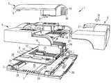
- FIG. 4the inventive housing of FIG. 1 in an exploded view.
- FIG. 5the first hood seen from the inside.
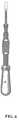
- FIG. 6is a perspective view of an embodiment of a mechanical tool, which is illustrated as a screwdriver.
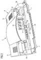
- FIG. 1shows the inventive housing 1 in an assembled state.
- the housingcontains electronic components of a telecommunications system. It essentially consists of a base housing part 2 and a housing cover 3 .
- the housing cover 3consists of a cover 4 , a first hood 5 and a second hood 6 .
- the housing 1is essentially rectangular in shape.
- the cover 4 and the two hoods 5 and 6are grouped symmetrically around the longitudinal center axis 10 .
- the housing 1features a convex curved front center surface 20 running concentrically to the longitudinal center axis 10 .
- the sides of the front center surface 20are adjoined by the wall sections 15 of the cover part 4 and wall sections 16 of the second hood 6 .
- the front center surface 20 forming a forwards-facing convex curveforms a continuous transition surface to the front surfaces of the side wall sections 15 and 16 , which gives the housing 1 an attractive exterior form.
- FIG. 2shows the inventive housing 1 in a view in which the second hood 6 is removed, which allows the connection area 11 to be seen.
- the connection area 11lies in a profiled recess extending backwards from the front side of the housing. In the connection area 11 different plug-in devices 24 , 32 , 33 for electrical connection of system terminations can be seen.
- the view shown in FIG. 3differs from that shown in FIG. 2 in that the first hood 5 is shown in a raised position. This reveals the extension area 12 with the extension printed circuit board 18 .
- the recess of the cover part 4continues into the extension area 12 and is broken through by plug-in openings 13 .
- the plug-in openings 13allow plug-in devices 23 to be seen which are accommodated on the main printed circuit board 8 .
- Extension circuit boards 18are plugged into the plug-in devices 23 ;
- the drawing of FIG. 3for example shows four plugged-in extension circuit boards 18 .
- the extension circuit boards 18are held on one of their bottom edges in guides 19 of the cover part 4 .
- Each extension circuit board 18features plug-in devices 24 on a side facing towards the connection area 11 .
- the plug-in devices 24are intended for the connection of user-side terminations and are accessible from the connection area 11 .
- FIG. 4shows an exploded view of the inventive housing 1 .
- the communication systemis now assembled so that the main printed circuit board 8 is placed on a surrounding support edge 22 of the base housing part 2 and the cover part 4 is placed on it (the guides 7 are used to guide the circuit board and the cover part 4 on assembly).
- the cover part 4is lowered, the locking clips 29 are deflected by the base part 2 .
- the locking clips 29engage in corresponding locking tabs of the cover 4 .
- the main printed circuit board 8is clamped between the base housing part 2 and the cover part 4 .
- the sequencethen continues with the first hood 5 being put on, the attachment tabs 9 being inserted and connected by means of the connection 39 ( FIG.
- the second hood 6is installed in a last step of assembly. This involves pushing the hood 6 onto the connection area in the direction of the arrow 31 and latching it by means snap-in hook 37 ( FIG. 5 ) to cover part 4 . This is done by turning it counterclockwise and does not require a mechanical tool.
- the twist locks 21assists in latching in the hood 6 .
- This constructionallows the second hood 6 to be easily removed manually and makes the connection area easily accessible from the user side.
- the rear wall of the base housing part 2features cutouts 26 in its edge area to which the incoming and outgoing lines can be attached, by cable ties for example.
- the keyhole-shaped slot 25is used for wall mounting of the housing 1 .
- break-out partsare provided which can be broken out from the opening depending on the capacity stage.
- the exemplary embodiment shownhas four mounting locations for sub-modules, each of which has an accessible interface area available. The fifth mounting location is used to accept shorter modules with no interface to the outside.
- plug-in devices 17are provided on the face of the main printed circuit board 8 by means of which the main printed circuit board 8 is electrically connected to further extension circuit boards 28 .
- the sides of these extension circuit boards 28are plugged into the main printed circuit board 8 and they run essentially in the plane of the main printed circuit board surface 27 . This enables an analog subscriber line interface 32 to be expanded in an expanded capacity stage into a digital subscriber interface 33 ( FIG. 2 ).
- FIG. 5shows the second hood 6 viewed from the direction of the connection area.
- the inventive housingessentially consists of four parts which are assembled using latches or snap-in hooks into a construction.
- the assemblyis simple and possible in a comparatively short time. Expensive means of connection, such as screws for example, are not required.
- a design of the housing made from plasticis very good. All parts of the housing cover 3 , as well as the base housing part, can be manufactured at low cost using injection molding.
Landscapes
- Engineering & Computer Science (AREA)
- Microelectronics & Electronic Packaging (AREA)
- Computer Networks & Wireless Communication (AREA)
- Casings For Electric Apparatus (AREA)
- Mounting Of Printed Circuit Boards And The Like (AREA)
- Telephone Set Structure (AREA)
Abstract
Description
- 1 Housing
- 2 Base housing part
- 3 Housing cover
- 4 Cover part
- 5 First hood
- 6 Second hood
- 7 Guides
- 8 Main printed circuit board
- 9 Insertion tab
- 10 Center longitudinal axis
- 11 Connection area
- 12 Extension area
- 13 First plug-in opening in4
- 14 Second plug-in openings and in5
- 15 side, front-side of the wall sections of4
- 16 side, front-side of the wall section of6
- 17 End face plug-in device
- 18 Extension circuit boards (subscriber)
- 19 Guides for18
- 20 Convex curved front center surface
- 21 Twist locks
- 22 Support edge
- 23 First plug-in device
- 24 Second plug-in device
- 25 Cutout, keyhole-shaped
- 26 Recesses
- 27 Main printed circuit board surface
- 28 Extension printed circuit board (digital)
- 29 Latching spring on2
- 30 Starting bevel
- 31 Arrow
- 32 Analog subscriber line termination
- 33 Digital subscriber line termination
- 36 Starting surfaces
- 37 Snap-in hooks of6
- 38 Cutout in4
- 39 Latching connection between4 and5
Claims (18)
Applications Claiming Priority (4)
| Application Number | Priority Date | Filing Date | Title |
|---|---|---|---|
| DE10336610ADE10336610A1 (en) | 2003-08-08 | 2003-08-08 | Housing for receiving printed circuit boards, the assembly of which forms at least parts of a communication system |
| DE10336610 | 2003-08-08 | ||
| DE10336610.5 | 2003-08-08 | ||
| PCT/EP2004/006103WO2005025245A1 (en) | 2003-08-08 | 2004-06-07 | Housing receiving printed circuit boards whose components form at least parts of a communication system |
Publications (2)
| Publication Number | Publication Date |
|---|---|
| US20080205006A1 US20080205006A1 (en) | 2008-08-28 |
| US7903429B2true US7903429B2 (en) | 2011-03-08 |
Family
ID=34177400
Family Applications (1)
| Application Number | Title | Priority Date | Filing Date |
|---|---|---|---|
| US10/567,618Expired - LifetimeUS7903429B2 (en) | 2003-08-08 | 2004-06-07 | Housing for receiving printed circuit boards whose components form at least parts of a communication system |
Country Status (11)
| Country | Link |
|---|---|
| US (1) | US7903429B2 (en) |
| EP (1) | EP1652389B1 (en) |
| JP (1) | JP4047902B2 (en) |
| KR (1) | KR101062035B1 (en) |
| CN (1) | CN100559890C (en) |
| BR (1) | BRPI0410827A (en) |
| DE (2) | DE10336610A1 (en) |
| IL (1) | IL170171A (en) |
| RU (1) | RU2344567C2 (en) |
| TW (1) | TWI252726B (en) |
| WO (1) | WO2005025245A1 (en) |
Cited By (3)
| Publication number | Priority date | Publication date | Assignee | Title |
|---|---|---|---|---|
| US20100124036A1 (en)* | 2008-11-20 | 2010-05-20 | Interplex Industries, Inc. | Solderless electronic component or capacitor mount assembly |
| US20110255254A1 (en)* | 2008-12-22 | 2011-10-20 | Sanden Corporation | Remote monitoring and control apparatus |
| US8758040B2 (en)* | 2012-11-29 | 2014-06-24 | Eaton Corporation | Systems and methods for aligning and connecting electrical components |
Families Citing this family (5)
| Publication number | Priority date | Publication date | Assignee | Title |
|---|---|---|---|---|
| WO2007109310A2 (en)* | 2006-03-21 | 2007-09-27 | Generonix, Inc. | System and method for extending dsl transmission range |
| JP5201964B2 (en)* | 2007-12-03 | 2013-06-05 | 三洋電機株式会社 | Image display device |
| US9028404B2 (en)* | 2010-07-28 | 2015-05-12 | Foster-Miller, Inc. | Physiological status monitoring system |
| CN103999562B (en)* | 2011-12-16 | 2017-05-17 | 瑞典爱立信有限公司 | Plug-in unit protection |
| CN116156818B (en)* | 2023-04-20 | 2023-09-08 | 昆明敏田科技有限公司 | A kind of printed circuit board and its carrier |
Citations (45)
| Publication number | Priority date | Publication date | Assignee | Title |
|---|---|---|---|---|
| US3684925A (en)* | 1971-02-01 | 1972-08-15 | Computer Transmission Corp | Housing and frame assembly for enclosing and supporting electronic apparatus |
| US4213013A (en)* | 1978-02-17 | 1980-07-15 | Bunker Ramo Corporation | Telephone network/subscriber interface device |
| US4303296A (en)* | 1978-05-03 | 1981-12-01 | Bunker Ramo Corporation | Modular interface connector |
| US4716499A (en)* | 1986-07-28 | 1987-12-29 | Hayes Microcomputer Products, Inc. | Enclosed circuit board assembly |
| US4749359A (en)* | 1987-08-27 | 1988-06-07 | Siecor Corporation | Security override network interface device |
| US4821150A (en)* | 1988-03-31 | 1989-04-11 | Hubbell Incorporated | Printed circuit board mounting for communication termination |
| US4827504A (en)* | 1987-03-04 | 1989-05-02 | Keptel, Inc. | Network interface enclosure |
| US4910770A (en)* | 1986-06-30 | 1990-03-20 | Keptel, Inc. | Network interface device and enclosure |
| US4945559A (en)* | 1987-12-30 | 1990-07-31 | Keptel, Inc. | Telephone network interface apparatus |
| US5130893A (en)* | 1990-01-17 | 1992-07-14 | Square D Company | Signal distribution system |
| US5398156A (en)* | 1993-03-22 | 1995-03-14 | Dell Usa, L.P. | Shielded computer printed circuit board retention apparatus |
| DE4342739A1 (en) | 1993-12-15 | 1995-06-22 | Telefonbau & Normalzeit Gmbh | Miniature telecommunications exchange installation |
| JPH0832267A (en) | 1994-07-11 | 1996-02-02 | Maspro Denkoh Corp | Case for electronic apparatus |
| US5521793A (en)* | 1994-07-21 | 1996-05-28 | Northern Telecom Limited | Wireless base station |
| US5528684A (en)* | 1994-09-02 | 1996-06-18 | Antec Corp. | Coaxial cable interface including security cover for demarcation point |
| US5552965A (en)* | 1993-04-02 | 1996-09-03 | Saia Ag | Control apparatus having a compact and accessible arrangement of printed circuit boards |
| US5568355A (en)* | 1994-02-25 | 1996-10-22 | Siemens Aktiengesellschaft | PCB housing with two-part terminal-access cover |
| US5633926A (en)* | 1995-04-19 | 1997-05-27 | Tii Industries, Inc. | Network interface enclosure |
| US5671126A (en)* | 1994-02-25 | 1997-09-23 | Siemens Aktiengesellschaft | Housing for the acceptance of equipped printed circuit boards |
| US5803292A (en)* | 1996-09-19 | 1998-09-08 | Lucent Technologies Inc. | Uniform building entrance protector housing construction with expandable splice chamber |
| US5832078A (en)* | 1996-08-09 | 1998-11-03 | Antec Corporation | Multiple jack and enclosure apparatus combination |
| US5901220A (en)* | 1997-02-28 | 1999-05-04 | The Whitaker Corporation | Network interface device |
| US5982619A (en)* | 1997-06-12 | 1999-11-09 | Harris Corporation | Housing for diverse cooling configuration printed circuit cards |
| EP0964586A2 (en) | 1998-06-08 | 1999-12-15 | DeTeWe - Deutsche Telephonwerke Aktiengesellschaft & Co. | Housing for a small telecommunication equipment |
| US6011831A (en)* | 1998-04-02 | 2000-01-04 | Antec Corporation | Network interface device having cavities for housing test circuitry |
| US6026160A (en)* | 1997-12-31 | 2000-02-15 | Siecor Operations, Llc | xDSL splitter interconnect module for network interface device |
| JP2000114739A (en) | 1998-09-30 | 2000-04-21 | Yazaki Corp | Electrical junction box |
| US6078661A (en)* | 1997-09-29 | 2000-06-20 | Lucent Technologies, Inc. | Modular network interface device |
| US6157714A (en)* | 1998-08-28 | 2000-12-05 | Lucent Technologies, Inc. | Modular layered network interface unit particularly suited to a two-layer arrangement |
| US6159022A (en)* | 1998-12-31 | 2000-12-12 | Hon Hai Precision Ind. Co., Ltd. | Universal electrical connector station |
| US6219252B1 (en)* | 1998-12-31 | 2001-04-17 | Hon Hai Precision Ind. Co., Ltd. | Universal docking station |
| US6229890B1 (en)* | 1997-09-29 | 2001-05-08 | Avaya Technology Corp. | Network interface device with automatic connector closure |
| US20010021103A1 (en)* | 2000-01-12 | 2001-09-13 | Omron Corporation | Control unit and method of manufacturing the same |
| US6292558B1 (en)* | 1987-01-06 | 2001-09-18 | Tii Industries, Inc. | Telephone network interface apparatus |
| US6307933B1 (en)* | 1996-12-09 | 2001-10-23 | Antec Corporation | Apparatus for providing a plurality of providers of subscriber service signals with easy access to at least one subscriber premises line |
| US6319018B1 (en)* | 2000-02-29 | 2001-11-20 | Avaya Technology Corp. | Circuit board electrical and physical connection system and method |
| US6322375B1 (en)* | 1997-09-29 | 2001-11-27 | Avaya Technology Corp. | Network interface device with circuit board architecture |
| JP2002043765A (en) | 2000-07-26 | 2002-02-08 | Sony Corp | Electronic apparatus |
| US20020050771A1 (en)* | 2000-10-26 | 2002-05-02 | Harro Krispin | Housing for a telecommunications system |
| US6488542B2 (en)* | 1997-11-17 | 2002-12-03 | Intel Corporation | Type III PCMCIA card with integrated receptacles for receiving standard communications plugs |
| US20030073338A1 (en)* | 2001-10-16 | 2003-04-17 | Adc Dsl Systems, Inc. | Housing for telecommunications module |
| US20030218867A1 (en)* | 2002-05-24 | 2003-11-27 | Adc Dsl Systems, Inc. | Housings for circuit cards |
| US6714647B1 (en)* | 1999-09-30 | 2004-03-30 | Avaya Technology Corp. | Network interface unit with subscriber line daughter boards |
| US6830458B2 (en)* | 2002-09-10 | 2004-12-14 | Sony Corporation | Apparatus incorporating electronic-parts-implementing board and a method for incorporating electronic-parts-implementing board |
| US6848946B2 (en)* | 2002-07-30 | 2005-02-01 | Tyco Eletro-Eletronica Ltda. | Electrical fuse realy box, apparatus, method and article of manufacture |
Family Cites Families (8)
| Publication number | Priority date | Publication date | Assignee | Title |
|---|---|---|---|---|
| FR2080309A5 (en)* | 1970-02-04 | 1971-11-12 | Robotron Veb K | |
| DE3737058C1 (en)* | 1987-10-28 | 1988-12-01 | Deutsche Telephonwerk Kabel | Housing for accommodating electrical telecommunications system assemblies |
| SU1499537A1 (en)* | 1988-01-28 | 1989-08-07 | И.А.Горбань | Case of electronic apparatus for accommodating and fastening printed circuit-boards |
| SU1721861A1 (en)* | 1990-04-06 | 1992-03-23 | Научно-производственное объединение "Старт" | Body of radio electronic device for arrangement and fixing of printed circuit boards |
| DE4207948A1 (en)* | 1992-03-10 | 1993-09-16 | Deutsche Telephonwerk Kabel | Telecommunication appts. with completely covered circuit boards - has polycarbonate cover extending over entire width as far as exchange line and terminal contact connections and mains cable connector |
| DE4242739A1 (en)* | 1992-12-17 | 1994-06-23 | Thomson Brandt Gmbh | Radio receiver monitoring system |
| ES2121226T3 (en)* | 1993-10-07 | 1998-11-16 | Raychem Sa Nv | ENVIRONMENTAL PROTECTION. |
| US5515240A (en)* | 1994-02-14 | 1996-05-07 | Winegard Company | Self-locking housing including tabs that bear against the sides of a printed circuit board to entrap the printed circuit board |
- 2003
- 2003-08-08DEDE10336610Apatent/DE10336610A1/ennot_activeWithdrawn
- 2004
- 2004-06-07EPEP04739645Apatent/EP1652389B1/ennot_activeExpired - Lifetime
- 2004-06-07CNCNB2004800037814Apatent/CN100559890C/ennot_activeExpired - Fee Related
- 2004-06-07JPJP2006500106Apatent/JP4047902B2/ennot_activeExpired - Fee Related
- 2004-06-07DEDE502004005844Tpatent/DE502004005844D1/ennot_activeExpired - Lifetime
- 2004-06-07BRBRPI0410827-2Apatent/BRPI0410827A/ennot_activeIP Right Cessation
- 2004-06-07RURU2005127858/09Apatent/RU2344567C2/enactive
- 2004-06-07USUS10/567,618patent/US7903429B2/ennot_activeExpired - Lifetime
- 2004-06-07WOPCT/EP2004/006103patent/WO2005025245A1/enactiveApplication Filing
- 2004-06-07KRKR1020067002651Apatent/KR101062035B1/ennot_activeExpired - Fee Related
- 2004-06-30TWTW093119273Apatent/TWI252726B/ennot_activeIP Right Cessation
- 2005
- 2005-08-09ILIL170171Apatent/IL170171A/enunknown
Patent Citations (46)
| Publication number | Priority date | Publication date | Assignee | Title |
|---|---|---|---|---|
| US3684925A (en)* | 1971-02-01 | 1972-08-15 | Computer Transmission Corp | Housing and frame assembly for enclosing and supporting electronic apparatus |
| US4213013A (en)* | 1978-02-17 | 1980-07-15 | Bunker Ramo Corporation | Telephone network/subscriber interface device |
| US4303296A (en)* | 1978-05-03 | 1981-12-01 | Bunker Ramo Corporation | Modular interface connector |
| US4910770A (en)* | 1986-06-30 | 1990-03-20 | Keptel, Inc. | Network interface device and enclosure |
| US4716499A (en)* | 1986-07-28 | 1987-12-29 | Hayes Microcomputer Products, Inc. | Enclosed circuit board assembly |
| US6292558B1 (en)* | 1987-01-06 | 2001-09-18 | Tii Industries, Inc. | Telephone network interface apparatus |
| US4827504A (en)* | 1987-03-04 | 1989-05-02 | Keptel, Inc. | Network interface enclosure |
| US4749359A (en)* | 1987-08-27 | 1988-06-07 | Siecor Corporation | Security override network interface device |
| US4945559A (en)* | 1987-12-30 | 1990-07-31 | Keptel, Inc. | Telephone network interface apparatus |
| US4821150A (en)* | 1988-03-31 | 1989-04-11 | Hubbell Incorporated | Printed circuit board mounting for communication termination |
| US5130893A (en)* | 1990-01-17 | 1992-07-14 | Square D Company | Signal distribution system |
| US5398156A (en)* | 1993-03-22 | 1995-03-14 | Dell Usa, L.P. | Shielded computer printed circuit board retention apparatus |
| US5552965A (en)* | 1993-04-02 | 1996-09-03 | Saia Ag | Control apparatus having a compact and accessible arrangement of printed circuit boards |
| DE4342739A1 (en) | 1993-12-15 | 1995-06-22 | Telefonbau & Normalzeit Gmbh | Miniature telecommunications exchange installation |
| US5568355A (en)* | 1994-02-25 | 1996-10-22 | Siemens Aktiengesellschaft | PCB housing with two-part terminal-access cover |
| US5671126A (en)* | 1994-02-25 | 1997-09-23 | Siemens Aktiengesellschaft | Housing for the acceptance of equipped printed circuit boards |
| JPH0832267A (en) | 1994-07-11 | 1996-02-02 | Maspro Denkoh Corp | Case for electronic apparatus |
| US5521793A (en)* | 1994-07-21 | 1996-05-28 | Northern Telecom Limited | Wireless base station |
| US5528684A (en)* | 1994-09-02 | 1996-06-18 | Antec Corp. | Coaxial cable interface including security cover for demarcation point |
| US5633926A (en)* | 1995-04-19 | 1997-05-27 | Tii Industries, Inc. | Network interface enclosure |
| US5832078A (en)* | 1996-08-09 | 1998-11-03 | Antec Corporation | Multiple jack and enclosure apparatus combination |
| US5803292A (en)* | 1996-09-19 | 1998-09-08 | Lucent Technologies Inc. | Uniform building entrance protector housing construction with expandable splice chamber |
| US6307933B1 (en)* | 1996-12-09 | 2001-10-23 | Antec Corporation | Apparatus for providing a plurality of providers of subscriber service signals with easy access to at least one subscriber premises line |
| US5901220A (en)* | 1997-02-28 | 1999-05-04 | The Whitaker Corporation | Network interface device |
| US5982619A (en)* | 1997-06-12 | 1999-11-09 | Harris Corporation | Housing for diverse cooling configuration printed circuit cards |
| US6322375B1 (en)* | 1997-09-29 | 2001-11-27 | Avaya Technology Corp. | Network interface device with circuit board architecture |
| US6229890B1 (en)* | 1997-09-29 | 2001-05-08 | Avaya Technology Corp. | Network interface device with automatic connector closure |
| US6078661A (en)* | 1997-09-29 | 2000-06-20 | Lucent Technologies, Inc. | Modular network interface device |
| US6488542B2 (en)* | 1997-11-17 | 2002-12-03 | Intel Corporation | Type III PCMCIA card with integrated receptacles for receiving standard communications plugs |
| US6026160A (en)* | 1997-12-31 | 2000-02-15 | Siecor Operations, Llc | xDSL splitter interconnect module for network interface device |
| US6011831A (en)* | 1998-04-02 | 2000-01-04 | Antec Corporation | Network interface device having cavities for housing test circuitry |
| EP0964586A2 (en) | 1998-06-08 | 1999-12-15 | DeTeWe - Deutsche Telephonwerke Aktiengesellschaft & Co. | Housing for a small telecommunication equipment |
| US6157714A (en)* | 1998-08-28 | 2000-12-05 | Lucent Technologies, Inc. | Modular layered network interface unit particularly suited to a two-layer arrangement |
| JP2000114739A (en) | 1998-09-30 | 2000-04-21 | Yazaki Corp | Electrical junction box |
| US6219252B1 (en)* | 1998-12-31 | 2001-04-17 | Hon Hai Precision Ind. Co., Ltd. | Universal docking station |
| US6159022A (en)* | 1998-12-31 | 2000-12-12 | Hon Hai Precision Ind. Co., Ltd. | Universal electrical connector station |
| US6714647B1 (en)* | 1999-09-30 | 2004-03-30 | Avaya Technology Corp. | Network interface unit with subscriber line daughter boards |
| US20010021103A1 (en)* | 2000-01-12 | 2001-09-13 | Omron Corporation | Control unit and method of manufacturing the same |
| US6319018B1 (en)* | 2000-02-29 | 2001-11-20 | Avaya Technology Corp. | Circuit board electrical and physical connection system and method |
| JP2002043765A (en) | 2000-07-26 | 2002-02-08 | Sony Corp | Electronic apparatus |
| US20020050771A1 (en)* | 2000-10-26 | 2002-05-02 | Harro Krispin | Housing for a telecommunications system |
| US20030073338A1 (en)* | 2001-10-16 | 2003-04-17 | Adc Dsl Systems, Inc. | Housing for telecommunications module |
| US6688919B2 (en)* | 2001-10-16 | 2004-02-10 | Adc Dsl Systems, Inc. | Housing for telecommunications module |
| US20030218867A1 (en)* | 2002-05-24 | 2003-11-27 | Adc Dsl Systems, Inc. | Housings for circuit cards |
| US6848946B2 (en)* | 2002-07-30 | 2005-02-01 | Tyco Eletro-Eletronica Ltda. | Electrical fuse realy box, apparatus, method and article of manufacture |
| US6830458B2 (en)* | 2002-09-10 | 2004-12-14 | Sony Corporation | Apparatus incorporating electronic-parts-implementing board and a method for incorporating electronic-parts-implementing board |
Cited By (4)
| Publication number | Priority date | Publication date | Assignee | Title |
|---|---|---|---|---|
| US20100124036A1 (en)* | 2008-11-20 | 2010-05-20 | Interplex Industries, Inc. | Solderless electronic component or capacitor mount assembly |
| US8305769B2 (en)* | 2008-11-20 | 2012-11-06 | Interplex Industries, Inc. | Solderless electronic component or capacitor mount assembly |
| US20110255254A1 (en)* | 2008-12-22 | 2011-10-20 | Sanden Corporation | Remote monitoring and control apparatus |
| US8758040B2 (en)* | 2012-11-29 | 2014-06-24 | Eaton Corporation | Systems and methods for aligning and connecting electrical components |
Also Published As
| Publication number | Publication date |
|---|---|
| CN100559890C (en) | 2009-11-11 |
| IL170171A (en) | 2010-11-30 |
| EP1652389B1 (en) | 2008-01-02 |
| TWI252726B (en) | 2006-04-01 |
| RU2005127858A (en) | 2006-05-27 |
| JP2006523011A (en) | 2006-10-05 |
| WO2005025245A1 (en) | 2005-03-17 |
| BRPI0410827A (en) | 2006-06-27 |
| DE10336610A1 (en) | 2005-03-10 |
| US20080205006A1 (en) | 2008-08-28 |
| KR20060058709A (en) | 2006-05-30 |
| TW200511917A (en) | 2005-03-16 |
| CN1748431A (en) | 2006-03-15 |
| JP4047902B2 (en) | 2008-02-13 |
| EP1652389A1 (en) | 2006-05-03 |
| KR101062035B1 (en) | 2011-09-02 |
| RU2344567C2 (en) | 2009-01-20 |
| DE502004005844D1 (en) | 2008-02-14 |
Similar Documents
| Publication | Publication Date | Title |
|---|---|---|
| US6608764B2 (en) | Telecommunications patch panel | |
| US6761594B2 (en) | DSX jack including sliding rear connector | |
| US7336497B2 (en) | Electronics housing | |
| JP3518678B2 (en) | Optical connector | |
| US7351116B2 (en) | Connecting element | |
| KR101076985B1 (en) | Patch panel for mounting on a wall or in a subrack | |
| CA2692827C (en) | Module assembly having interface module and insertable modular jack | |
| JP2809457B2 (en) | Communication box assembly | |
| AU749859B2 (en) | Patch panel and interlocking module | |
| JP2003158384A (en) | Angled patch panel with cable support for network cable rack | |
| US11272633B2 (en) | Electronic device having a printed circuit board | |
| US6241562B1 (en) | Digital cross connect/interconnect module | |
| US7903429B2 (en) | Housing for receiving printed circuit boards whose components form at least parts of a communication system | |
| US5839922A (en) | 110 wiring block interlock and interlocked blocks utilizing such | |
| EP3700035B1 (en) | A modular distribution box for cables | |
| GB2338352A (en) | Video data connector assembly | |
| JPS63140599A (en) | Communication equipment cabinet | |
| EP0801830B1 (en) | Insertion frame | |
| CA2614934A1 (en) | Distribution device | |
| WO2002039756A1 (en) | Retrofit patch and/or test panel | |
| WO1999048171A1 (en) | Modular network adapter | |
| WO1998033237A1 (en) | Housing for coaxial connectors | |
| EP1544961B1 (en) | Voice/data adapter kit | |
| HK1012788A1 (en) | Combination of electrical installation equipment and mounting element for installation channel |
Legal Events
| Date | Code | Title | Description |
|---|---|---|---|
| AS | Assignment | Owner name:SIEMENS AKTIENGESELLSCHAFT, GERMANY Free format text:ASSIGNMENT OF ASSIGNORS INTEREST;ASSIGNORS:FURSICH, WALTER;HARNISCHMACHER, FRIEDHELM;VERDING, MARKUS;REEL/FRAME:020944/0402;SIGNING DATES FROM 20050214 TO 20060214 Owner name:SIEMENS AKTIENGESELLSCHAFT,GERMANY Free format text:ASSIGNMENT OF ASSIGNORS INTEREST;ASSIGNORS:FURSICH, WALTER;HARNISCHMACHER, FRIEDHELM;VERDING, MARKUS;SIGNING DATES FROM 20050214 TO 20060214;REEL/FRAME:020944/0402 Owner name:SIEMENS AKTIENGESELLSCHAFT, GERMANY Free format text:ASSIGNMENT OF ASSIGNORS INTEREST;ASSIGNORS:FURSICH, WALTER;HARNISCHMACHER, FRIEDHELM;VERDING, MARKUS;SIGNING DATES FROM 20050214 TO 20060214;REEL/FRAME:020944/0402 | |
| STCF | Information on status: patent grant | Free format text:PATENTED CASE | |
| AS | Assignment | Owner name:SIEMENS ENTERPRISE COMMUNICATIONS GMBH & CO. KG, G Free format text:ASSIGNMENT OF ASSIGNORS INTEREST;ASSIGNOR:SIEMENS AKTIENGESELLSCHAFT;REEL/FRAME:028967/0427 Effective date:20120523 | |
| AS | Assignment | Owner name:UNIFY GMBH & CO. KG, GERMANY Free format text:CHANGE OF NAME;ASSIGNOR:SIEMENS ENTERPRISE COMMUNICATIONS GMBH & CO. KG;REEL/FRAME:033156/0114 Effective date:20131021 | |
| FPAY | Fee payment | Year of fee payment:4 | |
| FEPP | Fee payment procedure | Free format text:MAINTENANCE FEE REMINDER MAILED (ORIGINAL EVENT CODE: REM.); ENTITY STATUS OF PATENT OWNER: LARGE ENTITY | |
| FEPP | Fee payment procedure | Free format text:7.5 YR SURCHARGE - LATE PMT W/IN 6 MO, LARGE ENTITY (ORIGINAL EVENT CODE: M1555); ENTITY STATUS OF PATENT OWNER: LARGE ENTITY | |
| MAFP | Maintenance fee payment | Free format text:PAYMENT OF MAINTENANCE FEE, 8TH YEAR, LARGE ENTITY (ORIGINAL EVENT CODE: M1552); ENTITY STATUS OF PATENT OWNER: LARGE ENTITY Year of fee payment:8 | |
| MAFP | Maintenance fee payment | Free format text:PAYMENT OF MAINTENANCE FEE, 12TH YEAR, LARGE ENTITY (ORIGINAL EVENT CODE: M1553); ENTITY STATUS OF PATENT OWNER: LARGE ENTITY Year of fee payment:12 | |
| AS | Assignment | Owner name:UNIFY PATENTE GMBH & CO. KG, GERMANY Free format text:ASSIGNMENT OF ASSIGNORS INTEREST;ASSIGNOR:UNIFY GMBH & CO. KG;REEL/FRAME:065627/0001 Effective date:20140930 | |
| AS | Assignment | Owner name:CREDIT SUISSE AG, CAYMAN ISLANDS BRANCH, AS COLLATERAL AGENT, NEW YORK Free format text:SECURITY INTEREST;ASSIGNOR:UNIFY PATENTE GMBH & CO. KG;REEL/FRAME:066197/0333 Effective date:20231030 Owner name:CREDIT SUISSE AG, CAYMAN ISLANDS BRANCH, AS COLLATERAL AGENT, NEW YORK Free format text:SECURITY INTEREST;ASSIGNOR:UNIFY PATENTE GMBH & CO. KG;REEL/FRAME:066197/0299 Effective date:20231030 Owner name:CREDIT SUISSE AG, CAYMAN ISLANDS BRANCH, AS COLLATERAL AGENT, NEW YORK Free format text:SECURITY INTEREST;ASSIGNOR:UNIFY PATENTE GMBH & CO. KG;REEL/FRAME:066197/0073 Effective date:20231030 | |
| AS | Assignment | Owner name:UNIFY BETEILIGUNGSVERWALTUNG GMBH & CO. KG, GERMANY Free format text:CHANGE OF NAME;ASSIGNOR:UNIFY PATENTE GMBH & CO. KG;REEL/FRAME:069242/0312 Effective date:20240703 | |
| AS | Assignment | Owner name:WILMINGTON SAVINGS FUND SOCIETY, FSB, DELAWARE Free format text:NOTICE OF SUCCCESSION OF AGENCY - 3L;ASSIGNOR:UBS AG, STAMFORD BRANCH, AS LEGAL SUCCESSOR TO CREDIT SUISSE AG, CAYMAN ISLANDS BRANCH;REEL/FRAME:070006/0268 Effective date:20241203 Owner name:WILMINGTON SAVINGS FUND SOCIETY, FSB, DELAWARE Free format text:NOTICE OF SUCCCESSION OF AGENCY - PL;ASSIGNOR:UBS AG, STAMFORD BRANCH, AS LEGAL SUCCESSOR TO CREDIT SUISSE AG, CAYMAN ISLANDS BRANCH;REEL/FRAME:069895/0755 Effective date:20241203 Owner name:WILMINGTON SAVINGS FUND SOCIETY, FSB, DELAWARE Free format text:NOTICE OF SUCCCESSION OF AGENCY - 2L;ASSIGNOR:UBS AG, STAMFORD BRANCH, AS LEGAL SUCCESSOR TO CREDIT SUISSE AG, CAYMAN ISLANDS BRANCH;REEL/FRAME:069896/0001 Effective date:20241203 | |
| AS | Assignment | Owner name:MITEL (DELAWARE), INC., ARIZONA Free format text:RELEASE BY SECURED PARTY;ASSIGNOR:WILMINGTON SAVINGS FUND SOCIETY, FSB;REEL/FRAME:071712/0821 Effective date:20250620 Owner name:MITEL COMMUNICATIONS, INC., ARIZONA Free format text:RELEASE BY SECURED PARTY;ASSIGNOR:WILMINGTON SAVINGS FUND SOCIETY, FSB;REEL/FRAME:071712/0821 Effective date:20250620 Owner name:MITEL NETWORKS, INC., ARIZONA Free format text:RELEASE BY SECURED PARTY;ASSIGNOR:WILMINGTON SAVINGS FUND SOCIETY, FSB;REEL/FRAME:071712/0821 Effective date:20250620 Owner name:MITEL NETWORKS CORPORATION, ARIZONA Free format text:RELEASE BY SECURED PARTY;ASSIGNOR:WILMINGTON SAVINGS FUND SOCIETY, FSB;REEL/FRAME:071712/0821 Effective date:20250620 |