US7902679B2 - Structure and manufacturing method of a chip scale package with low fabrication cost, fine pitch and high reliability solder bump - Google Patents
Structure and manufacturing method of a chip scale package with low fabrication cost, fine pitch and high reliability solder bumpDownload PDFInfo
- Publication number
- US7902679B2 US7902679B2US11/981,138US98113807AUS7902679B2US 7902679 B2US7902679 B2US 7902679B2US 98113807 AUS98113807 AUS 98113807AUS 7902679 B2US7902679 B2US 7902679B2
- Authority
- US
- United States
- Prior art keywords
- layer
- solder
- substrate
- metal
- contact point
- Prior art date
- Legal status (The legal status is an assumption and is not a legal conclusion. Google has not performed a legal analysis and makes no representation as to the accuracy of the status listed.)
- Expired - Fee Related
Links
Images


Classifications
- H—ELECTRICITY
- H01—ELECTRIC ELEMENTS
- H01L—SEMICONDUCTOR DEVICES NOT COVERED BY CLASS H10
- H01L23/00—Details of semiconductor or other solid state devices
- H01L23/48—Arrangements for conducting electric current to or from the solid state body in operation, e.g. leads, terminal arrangements ; Selection of materials therefor
- H01L23/488—Arrangements for conducting electric current to or from the solid state body in operation, e.g. leads, terminal arrangements ; Selection of materials therefor consisting of soldered or bonded constructions
- H01L23/498—Leads, i.e. metallisations or lead-frames on insulating substrates, e.g. chip carriers
- H01L23/49811—Additional leads joined to the metallisation on the insulating substrate, e.g. pins, bumps, wires, flat leads
- H01L23/49816—Spherical bumps on the substrate for external connection, e.g. ball grid arrays [BGA]
- H—ELECTRICITY
- H01—ELECTRIC ELEMENTS
- H01L—SEMICONDUCTOR DEVICES NOT COVERED BY CLASS H10
- H01L24/00—Arrangements for connecting or disconnecting semiconductor or solid-state bodies; Methods or apparatus related thereto
- H01L24/01—Means for bonding being attached to, or being formed on, the surface to be connected, e.g. chip-to-package, die-attach, "first-level" interconnects; Manufacturing methods related thereto
- H01L24/02—Bonding areas ; Manufacturing methods related thereto
- H01L24/04—Structure, shape, material or disposition of the bonding areas prior to the connecting process
- H01L24/06—Structure, shape, material or disposition of the bonding areas prior to the connecting process of a plurality of bonding areas
- H—ELECTRICITY
- H01—ELECTRIC ELEMENTS
- H01L—SEMICONDUCTOR DEVICES NOT COVERED BY CLASS H10
- H01L24/00—Arrangements for connecting or disconnecting semiconductor or solid-state bodies; Methods or apparatus related thereto
- H01L24/01—Means for bonding being attached to, or being formed on, the surface to be connected, e.g. chip-to-package, die-attach, "first-level" interconnects; Manufacturing methods related thereto
- H01L24/10—Bump connectors ; Manufacturing methods related thereto
- H01L24/12—Structure, shape, material or disposition of the bump connectors prior to the connecting process
- H—ELECTRICITY
- H01—ELECTRIC ELEMENTS
- H01L—SEMICONDUCTOR DEVICES NOT COVERED BY CLASS H10
- H01L24/00—Arrangements for connecting or disconnecting semiconductor or solid-state bodies; Methods or apparatus related thereto
- H01L24/01—Means for bonding being attached to, or being formed on, the surface to be connected, e.g. chip-to-package, die-attach, "first-level" interconnects; Manufacturing methods related thereto
- H01L24/10—Bump connectors ; Manufacturing methods related thereto
- H01L24/15—Structure, shape, material or disposition of the bump connectors after the connecting process
- H01L24/17—Structure, shape, material or disposition of the bump connectors after the connecting process of a plurality of bump connectors
- H—ELECTRICITY
- H01—ELECTRIC ELEMENTS
- H01L—SEMICONDUCTOR DEVICES NOT COVERED BY CLASS H10
- H01L2224/00—Indexing scheme for arrangements for connecting or disconnecting semiconductor or solid-state bodies and methods related thereto as covered by H01L24/00
- H01L2224/01—Means for bonding being attached to, or being formed on, the surface to be connected, e.g. chip-to-package, die-attach, "first-level" interconnects; Manufacturing methods related thereto
- H01L2224/02—Bonding areas; Manufacturing methods related thereto
- H01L2224/04—Structure, shape, material or disposition of the bonding areas prior to the connecting process
- H01L2224/0401—Bonding areas specifically adapted for bump connectors, e.g. under bump metallisation [UBM]
- H—ELECTRICITY
- H01—ELECTRIC ELEMENTS
- H01L—SEMICONDUCTOR DEVICES NOT COVERED BY CLASS H10
- H01L2224/00—Indexing scheme for arrangements for connecting or disconnecting semiconductor or solid-state bodies and methods related thereto as covered by H01L24/00
- H01L2224/01—Means for bonding being attached to, or being formed on, the surface to be connected, e.g. chip-to-package, die-attach, "first-level" interconnects; Manufacturing methods related thereto
- H01L2224/02—Bonding areas; Manufacturing methods related thereto
- H01L2224/04—Structure, shape, material or disposition of the bonding areas prior to the connecting process
- H01L2224/04042—Bonding areas specifically adapted for wire connectors, e.g. wirebond pads
- H—ELECTRICITY
- H01—ELECTRIC ELEMENTS
- H01L—SEMICONDUCTOR DEVICES NOT COVERED BY CLASS H10
- H01L2224/00—Indexing scheme for arrangements for connecting or disconnecting semiconductor or solid-state bodies and methods related thereto as covered by H01L24/00
- H01L2224/01—Means for bonding being attached to, or being formed on, the surface to be connected, e.g. chip-to-package, die-attach, "first-level" interconnects; Manufacturing methods related thereto
- H01L2224/02—Bonding areas; Manufacturing methods related thereto
- H01L2224/04—Structure, shape, material or disposition of the bonding areas prior to the connecting process
- H01L2224/05—Structure, shape, material or disposition of the bonding areas prior to the connecting process of an individual bonding area
- H01L2224/0554—External layer
- H01L2224/0556—Disposition
- H01L2224/05571—Disposition the external layer being disposed in a recess of the surface
- H01L2224/05572—Disposition the external layer being disposed in a recess of the surface the external layer extending out of an opening
- H—ELECTRICITY
- H01—ELECTRIC ELEMENTS
- H01L—SEMICONDUCTOR DEVICES NOT COVERED BY CLASS H10
- H01L2224/00—Indexing scheme for arrangements for connecting or disconnecting semiconductor or solid-state bodies and methods related thereto as covered by H01L24/00
- H01L2224/01—Means for bonding being attached to, or being formed on, the surface to be connected, e.g. chip-to-package, die-attach, "first-level" interconnects; Manufacturing methods related thereto
- H01L2224/02—Bonding areas; Manufacturing methods related thereto
- H01L2224/04—Structure, shape, material or disposition of the bonding areas prior to the connecting process
- H01L2224/06—Structure, shape, material or disposition of the bonding areas prior to the connecting process of a plurality of bonding areas
- H01L2224/061—Disposition
- H01L2224/0612—Layout
- H01L2224/0613—Square or rectangular array
- H01L2224/06134—Square or rectangular array covering only portions of the surface to be connected
- H01L2224/06136—Covering only the central area of the surface to be connected, i.e. central arrangements
- H—ELECTRICITY
- H01—ELECTRIC ELEMENTS
- H01L—SEMICONDUCTOR DEVICES NOT COVERED BY CLASS H10
- H01L2224/00—Indexing scheme for arrangements for connecting or disconnecting semiconductor or solid-state bodies and methods related thereto as covered by H01L24/00
- H01L2224/01—Means for bonding being attached to, or being formed on, the surface to be connected, e.g. chip-to-package, die-attach, "first-level" interconnects; Manufacturing methods related thereto
- H01L2224/10—Bump connectors; Manufacturing methods related thereto
- H01L2224/12—Structure, shape, material or disposition of the bump connectors prior to the connecting process
- H01L2224/13—Structure, shape, material or disposition of the bump connectors prior to the connecting process of an individual bump connector
- H01L2224/13001—Core members of the bump connector
- H01L2224/13005—Structure
- H01L2224/13007—Bump connector smaller than the underlying bonding area, e.g. than the under bump metallisation [UBM]
- H—ELECTRICITY
- H01—ELECTRIC ELEMENTS
- H01L—SEMICONDUCTOR DEVICES NOT COVERED BY CLASS H10
- H01L2224/00—Indexing scheme for arrangements for connecting or disconnecting semiconductor or solid-state bodies and methods related thereto as covered by H01L24/00
- H01L2224/01—Means for bonding being attached to, or being formed on, the surface to be connected, e.g. chip-to-package, die-attach, "first-level" interconnects; Manufacturing methods related thereto
- H01L2224/10—Bump connectors; Manufacturing methods related thereto
- H01L2224/12—Structure, shape, material or disposition of the bump connectors prior to the connecting process
- H01L2224/13—Structure, shape, material or disposition of the bump connectors prior to the connecting process of an individual bump connector
- H01L2224/13001—Core members of the bump connector
- H01L2224/1301—Shape
- H01L2224/13016—Shape in side view
- H01L2224/13017—Shape in side view being non uniform along the bump connector
- H—ELECTRICITY
- H01—ELECTRIC ELEMENTS
- H01L—SEMICONDUCTOR DEVICES NOT COVERED BY CLASS H10
- H01L2224/00—Indexing scheme for arrangements for connecting or disconnecting semiconductor or solid-state bodies and methods related thereto as covered by H01L24/00
- H01L2224/01—Means for bonding being attached to, or being formed on, the surface to be connected, e.g. chip-to-package, die-attach, "first-level" interconnects; Manufacturing methods related thereto
- H01L2224/10—Bump connectors; Manufacturing methods related thereto
- H01L2224/12—Structure, shape, material or disposition of the bump connectors prior to the connecting process
- H01L2224/13—Structure, shape, material or disposition of the bump connectors prior to the connecting process of an individual bump connector
- H01L2224/13001—Core members of the bump connector
- H01L2224/1302—Disposition
- H01L2224/13023—Disposition the whole bump connector protruding from the surface
- H—ELECTRICITY
- H01—ELECTRIC ELEMENTS
- H01L—SEMICONDUCTOR DEVICES NOT COVERED BY CLASS H10
- H01L2224/00—Indexing scheme for arrangements for connecting or disconnecting semiconductor or solid-state bodies and methods related thereto as covered by H01L24/00
- H01L2224/01—Means for bonding being attached to, or being formed on, the surface to be connected, e.g. chip-to-package, die-attach, "first-level" interconnects; Manufacturing methods related thereto
- H01L2224/10—Bump connectors; Manufacturing methods related thereto
- H01L2224/12—Structure, shape, material or disposition of the bump connectors prior to the connecting process
- H01L2224/13—Structure, shape, material or disposition of the bump connectors prior to the connecting process of an individual bump connector
- H01L2224/13001—Core members of the bump connector
- H01L2224/13075—Plural core members
- H01L2224/1308—Plural core members being stacked
- H01L2224/13083—Three-layer arrangements
- H—ELECTRICITY
- H01—ELECTRIC ELEMENTS
- H01L—SEMICONDUCTOR DEVICES NOT COVERED BY CLASS H10
- H01L2224/00—Indexing scheme for arrangements for connecting or disconnecting semiconductor or solid-state bodies and methods related thereto as covered by H01L24/00
- H01L2224/01—Means for bonding being attached to, or being formed on, the surface to be connected, e.g. chip-to-package, die-attach, "first-level" interconnects; Manufacturing methods related thereto
- H01L2224/10—Bump connectors; Manufacturing methods related thereto
- H01L2224/12—Structure, shape, material or disposition of the bump connectors prior to the connecting process
- H01L2224/13—Structure, shape, material or disposition of the bump connectors prior to the connecting process of an individual bump connector
- H01L2224/13001—Core members of the bump connector
- H01L2224/13099—Material
- H01L2224/131—Material with a principal constituent of the material being a metal or a metalloid, e.g. boron [B], silicon [Si], germanium [Ge], arsenic [As], antimony [Sb], tellurium [Te] and polonium [Po], and alloys thereof
- H01L2224/13138—Material with a principal constituent of the material being a metal or a metalloid, e.g. boron [B], silicon [Si], germanium [Ge], arsenic [As], antimony [Sb], tellurium [Te] and polonium [Po], and alloys thereof the principal constituent melting at a temperature of greater than or equal to 950°C and less than 1550°C
- H01L2224/13147—Copper [Cu] as principal constituent
- H—ELECTRICITY
- H01—ELECTRIC ELEMENTS
- H01L—SEMICONDUCTOR DEVICES NOT COVERED BY CLASS H10
- H01L2224/00—Indexing scheme for arrangements for connecting or disconnecting semiconductor or solid-state bodies and methods related thereto as covered by H01L24/00
- H01L2224/01—Means for bonding being attached to, or being formed on, the surface to be connected, e.g. chip-to-package, die-attach, "first-level" interconnects; Manufacturing methods related thereto
- H01L2224/10—Bump connectors; Manufacturing methods related thereto
- H01L2224/12—Structure, shape, material or disposition of the bump connectors prior to the connecting process
- H01L2224/13—Structure, shape, material or disposition of the bump connectors prior to the connecting process of an individual bump connector
- H01L2224/13001—Core members of the bump connector
- H01L2224/13099—Material
- H01L2224/131—Material with a principal constituent of the material being a metal or a metalloid, e.g. boron [B], silicon [Si], germanium [Ge], arsenic [As], antimony [Sb], tellurium [Te] and polonium [Po], and alloys thereof
- H01L2224/13138—Material with a principal constituent of the material being a metal or a metalloid, e.g. boron [B], silicon [Si], germanium [Ge], arsenic [As], antimony [Sb], tellurium [Te] and polonium [Po], and alloys thereof the principal constituent melting at a temperature of greater than or equal to 950°C and less than 1550°C
- H01L2224/13155—Nickel [Ni] as principal constituent
- H—ELECTRICITY
- H01—ELECTRIC ELEMENTS
- H01L—SEMICONDUCTOR DEVICES NOT COVERED BY CLASS H10
- H01L2224/00—Indexing scheme for arrangements for connecting or disconnecting semiconductor or solid-state bodies and methods related thereto as covered by H01L24/00
- H01L2224/01—Means for bonding being attached to, or being formed on, the surface to be connected, e.g. chip-to-package, die-attach, "first-level" interconnects; Manufacturing methods related thereto
- H01L2224/10—Bump connectors; Manufacturing methods related thereto
- H01L2224/15—Structure, shape, material or disposition of the bump connectors after the connecting process
- H01L2224/16—Structure, shape, material or disposition of the bump connectors after the connecting process of an individual bump connector
- H—ELECTRICITY
- H01—ELECTRIC ELEMENTS
- H01L—SEMICONDUCTOR DEVICES NOT COVERED BY CLASS H10
- H01L24/00—Arrangements for connecting or disconnecting semiconductor or solid-state bodies; Methods or apparatus related thereto
- H01L24/01—Means for bonding being attached to, or being formed on, the surface to be connected, e.g. chip-to-package, die-attach, "first-level" interconnects; Manufacturing methods related thereto
- H01L24/10—Bump connectors ; Manufacturing methods related thereto
- H01L24/15—Structure, shape, material or disposition of the bump connectors after the connecting process
- H01L24/16—Structure, shape, material or disposition of the bump connectors after the connecting process of an individual bump connector
- H—ELECTRICITY
- H01—ELECTRIC ELEMENTS
- H01L—SEMICONDUCTOR DEVICES NOT COVERED BY CLASS H10
- H01L2924/00—Indexing scheme for arrangements or methods for connecting or disconnecting semiconductor or solid-state bodies as covered by H01L24/00
- H01L2924/0001—Technical content checked by a classifier
- H01L2924/00013—Fully indexed content
- H—ELECTRICITY
- H01—ELECTRIC ELEMENTS
- H01L—SEMICONDUCTOR DEVICES NOT COVERED BY CLASS H10
- H01L2924/00—Indexing scheme for arrangements or methods for connecting or disconnecting semiconductor or solid-state bodies as covered by H01L24/00
- H01L2924/01—Chemical elements
- H01L2924/01005—Boron [B]
- H—ELECTRICITY
- H01—ELECTRIC ELEMENTS
- H01L—SEMICONDUCTOR DEVICES NOT COVERED BY CLASS H10
- H01L2924/00—Indexing scheme for arrangements or methods for connecting or disconnecting semiconductor or solid-state bodies as covered by H01L24/00
- H01L2924/01—Chemical elements
- H01L2924/01006—Carbon [C]
- H—ELECTRICITY
- H01—ELECTRIC ELEMENTS
- H01L—SEMICONDUCTOR DEVICES NOT COVERED BY CLASS H10
- H01L2924/00—Indexing scheme for arrangements or methods for connecting or disconnecting semiconductor or solid-state bodies as covered by H01L24/00
- H01L2924/01—Chemical elements
- H01L2924/01013—Aluminum [Al]
- H—ELECTRICITY
- H01—ELECTRIC ELEMENTS
- H01L—SEMICONDUCTOR DEVICES NOT COVERED BY CLASS H10
- H01L2924/00—Indexing scheme for arrangements or methods for connecting or disconnecting semiconductor or solid-state bodies as covered by H01L24/00
- H01L2924/01—Chemical elements
- H01L2924/01014—Silicon [Si]
- H—ELECTRICITY
- H01—ELECTRIC ELEMENTS
- H01L—SEMICONDUCTOR DEVICES NOT COVERED BY CLASS H10
- H01L2924/00—Indexing scheme for arrangements or methods for connecting or disconnecting semiconductor or solid-state bodies as covered by H01L24/00
- H01L2924/01—Chemical elements
- H01L2924/01015—Phosphorus [P]
- H—ELECTRICITY
- H01—ELECTRIC ELEMENTS
- H01L—SEMICONDUCTOR DEVICES NOT COVERED BY CLASS H10
- H01L2924/00—Indexing scheme for arrangements or methods for connecting or disconnecting semiconductor or solid-state bodies as covered by H01L24/00
- H01L2924/01—Chemical elements
- H01L2924/01018—Argon [Ar]
- H—ELECTRICITY
- H01—ELECTRIC ELEMENTS
- H01L—SEMICONDUCTOR DEVICES NOT COVERED BY CLASS H10
- H01L2924/00—Indexing scheme for arrangements or methods for connecting or disconnecting semiconductor or solid-state bodies as covered by H01L24/00
- H01L2924/01—Chemical elements
- H01L2924/01022—Titanium [Ti]
- H—ELECTRICITY
- H01—ELECTRIC ELEMENTS
- H01L—SEMICONDUCTOR DEVICES NOT COVERED BY CLASS H10
- H01L2924/00—Indexing scheme for arrangements or methods for connecting or disconnecting semiconductor or solid-state bodies as covered by H01L24/00
- H01L2924/01—Chemical elements
- H01L2924/01029—Copper [Cu]
- H—ELECTRICITY
- H01—ELECTRIC ELEMENTS
- H01L—SEMICONDUCTOR DEVICES NOT COVERED BY CLASS H10
- H01L2924/00—Indexing scheme for arrangements or methods for connecting or disconnecting semiconductor or solid-state bodies as covered by H01L24/00
- H01L2924/01—Chemical elements
- H01L2924/01033—Arsenic [As]
- H—ELECTRICITY
- H01—ELECTRIC ELEMENTS
- H01L—SEMICONDUCTOR DEVICES NOT COVERED BY CLASS H10
- H01L2924/00—Indexing scheme for arrangements or methods for connecting or disconnecting semiconductor or solid-state bodies as covered by H01L24/00
- H01L2924/01—Chemical elements
- H01L2924/01042—Molybdenum [Mo]
- H—ELECTRICITY
- H01—ELECTRIC ELEMENTS
- H01L—SEMICONDUCTOR DEVICES NOT COVERED BY CLASS H10
- H01L2924/00—Indexing scheme for arrangements or methods for connecting or disconnecting semiconductor or solid-state bodies as covered by H01L24/00
- H01L2924/01—Chemical elements
- H01L2924/0105—Tin [Sn]
- H—ELECTRICITY
- H01—ELECTRIC ELEMENTS
- H01L—SEMICONDUCTOR DEVICES NOT COVERED BY CLASS H10
- H01L2924/00—Indexing scheme for arrangements or methods for connecting or disconnecting semiconductor or solid-state bodies as covered by H01L24/00
- H01L2924/01—Chemical elements
- H01L2924/01073—Tantalum [Ta]
- H—ELECTRICITY
- H01—ELECTRIC ELEMENTS
- H01L—SEMICONDUCTOR DEVICES NOT COVERED BY CLASS H10
- H01L2924/00—Indexing scheme for arrangements or methods for connecting or disconnecting semiconductor or solid-state bodies as covered by H01L24/00
- H01L2924/01—Chemical elements
- H01L2924/01074—Tungsten [W]
- H—ELECTRICITY
- H01—ELECTRIC ELEMENTS
- H01L—SEMICONDUCTOR DEVICES NOT COVERED BY CLASS H10
- H01L2924/00—Indexing scheme for arrangements or methods for connecting or disconnecting semiconductor or solid-state bodies as covered by H01L24/00
- H01L2924/01—Chemical elements
- H01L2924/01075—Rhenium [Re]
- H—ELECTRICITY
- H01—ELECTRIC ELEMENTS
- H01L—SEMICONDUCTOR DEVICES NOT COVERED BY CLASS H10
- H01L2924/00—Indexing scheme for arrangements or methods for connecting or disconnecting semiconductor or solid-state bodies as covered by H01L24/00
- H01L2924/01—Chemical elements
- H01L2924/01078—Platinum [Pt]
- H—ELECTRICITY
- H01—ELECTRIC ELEMENTS
- H01L—SEMICONDUCTOR DEVICES NOT COVERED BY CLASS H10
- H01L2924/00—Indexing scheme for arrangements or methods for connecting or disconnecting semiconductor or solid-state bodies as covered by H01L24/00
- H01L2924/01—Chemical elements
- H01L2924/01079—Gold [Au]
- H—ELECTRICITY
- H01—ELECTRIC ELEMENTS
- H01L—SEMICONDUCTOR DEVICES NOT COVERED BY CLASS H10
- H01L2924/00—Indexing scheme for arrangements or methods for connecting or disconnecting semiconductor or solid-state bodies as covered by H01L24/00
- H01L2924/01—Chemical elements
- H01L2924/01082—Lead [Pb]
- H—ELECTRICITY
- H01—ELECTRIC ELEMENTS
- H01L—SEMICONDUCTOR DEVICES NOT COVERED BY CLASS H10
- H01L2924/00—Indexing scheme for arrangements or methods for connecting or disconnecting semiconductor or solid-state bodies as covered by H01L24/00
- H01L2924/013—Alloys
- H01L2924/014—Solder alloys
- H—ELECTRICITY
- H01—ELECTRIC ELEMENTS
- H01L—SEMICONDUCTOR DEVICES NOT COVERED BY CLASS H10
- H01L2924/00—Indexing scheme for arrangements or methods for connecting or disconnecting semiconductor or solid-state bodies as covered by H01L24/00
- H01L2924/049—Nitrides composed of metals from groups of the periodic table
- H01L2924/0494—4th Group
- H01L2924/04941—TiN
- H—ELECTRICITY
- H01—ELECTRIC ELEMENTS
- H01L—SEMICONDUCTOR DEVICES NOT COVERED BY CLASS H10
- H01L2924/00—Indexing scheme for arrangements or methods for connecting or disconnecting semiconductor or solid-state bodies as covered by H01L24/00
- H01L2924/10—Details of semiconductor or other solid state devices to be connected
- H01L2924/11—Device type
- H01L2924/12—Passive devices, e.g. 2 terminal devices
- H01L2924/1204—Optical Diode
- H01L2924/12044—OLED
- H—ELECTRICITY
- H01—ELECTRIC ELEMENTS
- H01L—SEMICONDUCTOR DEVICES NOT COVERED BY CLASS H10
- H01L2924/00—Indexing scheme for arrangements or methods for connecting or disconnecting semiconductor or solid-state bodies as covered by H01L24/00
- H01L2924/10—Details of semiconductor or other solid state devices to be connected
- H01L2924/11—Device type
- H01L2924/14—Integrated circuits
- H—ELECTRICITY
- H01—ELECTRIC ELEMENTS
- H01L—SEMICONDUCTOR DEVICES NOT COVERED BY CLASS H10
- H01L2924/00—Indexing scheme for arrangements or methods for connecting or disconnecting semiconductor or solid-state bodies as covered by H01L24/00
- H01L2924/15—Details of package parts other than the semiconductor or other solid state devices to be connected
- H01L2924/151—Die mounting substrate
- H01L2924/153—Connection portion
- H01L2924/1531—Connection portion the connection portion being formed only on the surface of the substrate opposite to the die mounting surface
- H01L2924/15311—Connection portion the connection portion being formed only on the surface of the substrate opposite to the die mounting surface being a ball array, e.g. BGA
- H—ELECTRICITY
- H01—ELECTRIC ELEMENTS
- H01L—SEMICONDUCTOR DEVICES NOT COVERED BY CLASS H10
- H01L2924/00—Indexing scheme for arrangements or methods for connecting or disconnecting semiconductor or solid-state bodies as covered by H01L24/00
- H01L2924/15—Details of package parts other than the semiconductor or other solid state devices to be connected
- H01L2924/181—Encapsulation
- H—ELECTRICITY
- H01—ELECTRIC ELEMENTS
- H01L—SEMICONDUCTOR DEVICES NOT COVERED BY CLASS H10
- H01L2924/00—Indexing scheme for arrangements or methods for connecting or disconnecting semiconductor or solid-state bodies as covered by H01L24/00
- H01L2924/30—Technical effects
- H01L2924/301—Electrical effects
- H01L2924/30105—Capacitance
- H—ELECTRICITY
- H01—ELECTRIC ELEMENTS
- H01L—SEMICONDUCTOR DEVICES NOT COVERED BY CLASS H10
- H01L2924/00—Indexing scheme for arrangements or methods for connecting or disconnecting semiconductor or solid-state bodies as covered by H01L24/00
- H01L2924/30—Technical effects
- H01L2924/35—Mechanical effects
- H01L2924/351—Thermal stress
Definitions
- the inventionrelates to the fabrication of integrated circuit devices, and more particularly, to a method and package for packaging semiconductor devices.
- BGABall Grid Array
- CGAColumn Grid Array
- BGABall Grid Array
- BGAis an array of solder balls placed on a chip carrier. The balls contact a printed circuit board in an array configuration where, after reheat, the balls connect the chip to the printed circuit board.
- BGA'sare known with 40, 50 and 60 mil spacings.
- Flip-chip technologyfabricates bumps (typically Pb/Sn solders) on aluminum pads on a semiconductor device.
- the bumpsare interconnected directly to the package media, which are usually ceramic or plastic based.
- the flip-chipis bonded face down to the package medium through the shortest paths.
- Chip-On-Board (COB) techniquesare used to attach semiconductor die to a printed circuit board; these techniques include the technical disciplines of flip chip attachment, wirebonding, and tape automated bonding (TAB).
- Flip chip attachmentconsists of attaching a flip chip to a printed circuit board or to another substrate.
- a flip chipis a semiconductor chip that has a pattern or arrays of terminals that are spaced around an active surface area of the flip chip, allowing for face down mounting of the flip chip to a substrate.
- the flip chip active surfacehas one of the following electrical connectors: BGA (wherein an array of minute solder balls is created on the surface of the flip chip that attaches to the substrate); Slightly Larger than Integrated Circuit Carrier (SLICC) (which is similar to the BGA but has a smaller solder ball pitch and diameter than the BGA); a Pin Grid Array (PGA) (wherein an array of small pins extends substantially perpendicularly from the attachment surface of a flip chip, such that the pins conform to a specific arrangement on a printed circuit board or other substrate for attachment thereto).
- BGAwherein an array of minute solder balls is created on the surface of the flip chip that attaches to the substrate
- SLICCSlightly Larger than Integrated Circuit Carrier
- PGAPin Grid Array
- the solder or other conductive ball arrangement on the flip chipmust be a mirror image of the connecting bond pads on the printed circuit board so that precise connection can be made.
- Bond padsare generally used to wire device elements and to provide exposed contact regions of the die. These contact regions are suitable for wiring the die to components that are external to the die.
- An exampleis where a bond wire is attached to a bond pad of a semiconductor die at one end and to a portion of a Printed Circuit Board at the other end of the wire.
- the artis constantly striving to achieve improvements in the creation of bond pads that simplify the manufacturing process while enhancing bond pad reliability.
- bonds padsMaterials that are typically used for bond pads include metallic materials, such as tungsten and aluminum, while heavily doped polysilicon can also be used for contacting material.
- the bond padis formed on the top surface of the semiconductor device whereby the electrically conducting material is frequently embedded in an insulating layer of dielectric.
- polysiliconcan be doped with an n-type dopant for contacting N-regions while it can be doped with p-type dopant for contacting P-regions. This approach of doping avoids inter-diffusion of the dopants and dopant migration. It is clear that low contact resistance for the bond pad area is required while concerns of avoidance of moisture or chemical solvent absorption, thin film adhesion characteristics, delamination and cracking play an important part in the creation of bond pads.
- the conventional processing sequence that is used to create an aluminum bond padstarts with a semiconductor surface, typically the surface of a silicon single crystalline substrate.
- a layer of Intra Metal Dielectric (IMD)is deposited over the surface, a layer of metal, typically aluminum, is deposited over the surface of the layer of IMD.
- the layer of metalis patterned and etched typically using a layer of photoresist and conventional methods of photolithography and etching.
- a layer of passivationis deposited over the layer of IMD.
- An opening that aligns with the bond padis created in the layer of passivation, again using methods of photolithography and etching.
- FIGS. 1 through 4show an example of one of the methods that is used to create an interconnect bump.
- a semiconductor surface 10has been provided with a metal contact pad 14 ; the semiconductor surface 10 is protected with a layer 12 of passivation.
- An opening 19has been created in the layer 12 of passivation; the surface of the metal contact pad 14 is exposed through this opening 19 .
- a dielectric layer 16is deposited over the surface of the layer 12 of passivation.
- the layer 16 of dielectricis patterned and etched, creating an opening 21 in the layer 16 of dielectric that aligns with the metal pad 14 and that partially exposes the surface of the metal pad 14 .
- a layer 18 of metalis created over the layer 16 of dielectric; layer 18 of metal is in contact with the surface of the metal pad 14 inside opening 21 .
- the region of layer 18 of metal that is above the metal pad 14will, at a later point in the processing, form a pedestal over which the interconnect bump will be formed.
- This pedestalcan be further extended in a vertical direction by the deposition and patterning of one or more additional layers that may contain a photoresist or a dielectric material; these additional layers are not shown in FIG. 2 .
- These layersessentially have the shape of layer 16 and are removed during one of the final processing steps that is applied for the formation of the interconnect bump.
- a layer of photoresist(not shown) is deposited, patterned and etched, creating an opening that aligns with the contact pad 14 .
- a layer 20 of metalsuch as copper or nickel, shown in FIG. 3 , that forms an integral part of the pedestal of the to be created interconnect bump, is next electroplated in the opening created in the layer of photoresist and on the surface of the layer 18 of metal, whereby the layer 18 serves as the lower electrode during the plating process.
- Layer 20 in prior art applicationshas a thickness of between about 1 and 10 ⁇ m with a typical value of about 5 ⁇ m.
- the final layer 22 of solderis electroplated on the surface of layer 20 .
- the patterned layer of photoresistis then removed.
- the layer 18 of metalis next etched, as in FIG. 4 , leaving in place only the pedestal for the interconnect bump. During this etch process the deposited layers 20 and 22 serve as a mask. If, as indicated above, additional layers of dielectric or photoresist have been deposited for the further shaping of pedestal 18 in FIG. 2 , these layers are also removed at this time.
- solder paste or flux(not shown) is now applied to the layer 22 of solder, and the solder 22 is melted in a reflow surface typically under a nitrogen atmosphere, creating the spherically shaped interconnect bump 22 that is shown in FIG. 4 .
- BLM layersare successive and overlying layers of chrome, copper and gold, whereby the chrome is used to enhance adhesion with an underlying aluminum contact pad, the copper layer serves to prevent diffusion of solder materials into underlying layers, while the gold layer serves to prevent oxidation of the surface of the copper layer.
- the BLM layeris layer 18 of FIGS. 2 through 4 .
- Increased device densitybrings with it increased closeness of components and elements that are part of the created semiconductor devices. This increased closeness is expressed as a reduction in the spacing or “pitch” between elements of a semiconductor device.
- State-of-the-art technologyuses solder bumps having a pitch of about 200 ⁇ m, which imposes a limitation on further increasing device density.
- the limitation in further reducing the pitch of solder bumpsis imposed by concerns of reliability, which impose a relatively large ball size for the solder bump. This relatively large solder ball restricts further reducing the solder ball pitch.
- solder bumpsare used as interconnections between I/O bond pads and a substrate or printed circuit board.
- a large solder ballbrings with it high standoff since a solder ball with high standoff has better thermal performance (CTE mismatching is easier to avoid resulting in reduced thermal stress on the solder balls).
- Large solder ballsare therefore required in order to maintain interconnect reliability.
- Low-alpha solderis applied to avoid soft error (electrical or functional errors) from occurring, thereby eliminating the potential for inadvertent memory discharge and incorrect setting of the voltage (1 or 0).
- the inventionaddresses concerns of creating a BGA type package whereby the pitch of the solder ball or solder bump of the device interconnect is in the range of 200 ⁇ m or less.
- the conventional, state-of-the-art solder processruns into limitations for such a fine interconnect pad pitch, the invention provides a method and a package for attaching devices having very small ball pitch to an interconnect medium such as a Printed Circuit Board.
- a principal objective of the inventionis to provide a method of creating a fine-pitch solder bump.
- Another objective of the inventionis to provide a method of creating smaller solder bumps, further allowing for the creation of fine-pitched solder bumps.
- Another objective of the inventionis to provide a cost-effective method to create a fine-pitch solder bump of high reliability, due to the increased height of the solder bump. This objective is based on the belief that solder bump reliability improves proportionally to the square of the distance between the solder ball and the underlying substrate.
- Another objective of the inventionis to provide a cost-effective way of creating a solder bump. This cost-effective way is realized by using standard solder material and therewith eliminating the need for expensive “low- ⁇ solder”.
- Another objective of the inventionis to provide a cost-effective method of creating a fine-pitch solder bump by reducing the alpha-effect on memory products.
- Another objective of the inventionis to provide a method of creating solder bumps which allows an easy method of cleaning flux after the process of creating the solder bump has been completed.
- Another objective of the inventionis to provide a method of creating solder bumps which allows easy application of underfill.
- Another objective of the inventionis to provide a method for applying fine pitch solder bumps directly to the I/O pads of a semiconductor device, without a redistribution interface, and bonding the semiconductor device directly to a Ball Grid Array substrate using the flip-chip bonding approach.
- Another objective of the inventionis to provide a method for shortening the interconnection between a semiconductor device and the substrate on which the device is mounted, thus improving the electrical performance of the device.
- Yet another objective of the inventionis to eliminate conventional methods of re-distribution of device I/O interconnect, thereby making packaging of the device more cost-effective and eliminating performance degradation.
- a still further objective of the inventionis to improve chip accessibility during testing of the device, thus eliminating the need for special test fixtures.
- a still further objective of the inventionis to improve performance and device reliability of BGA packages that are used for the mounting of semiconductor devices having small-pitch I/O interconnect bumps.
- a still further objective of the inventionis to perform Chip Scale Packaging (CSP) without re-distribution, including for various pad designs such as peripheral or central pad designs.
- CSPChip Scale Packaging
- a still further objective of the inventionis to provide a method of mounting small-pitch semiconductor devices in such a manner that flux removal and the dispensing of device encapsulants is improved.
- a new method and packageis provided for the mounting of semiconductor devices that have been provided with small-pitch Input/Output interconnect bumps.
- Fine pitch solder bumpsconsisting of pillar metal and a solder bump, are applied directly to the I/O pads of the semiconductor device, the device is then flip-chip bonded to a substrate. Dummy bumps may be provided for cases where the I/O pads of the device are arranged such that additional mechanical support for the device is required.
- FIGS. 1 through 4show a prior art method of creating a solder bump overlying a point of electrical contact, as follows:
- FIG. 1shows a cross section of a semiconductor surface on the surface of which a contact pad has been created; the semiconductor surface is covered with a patterned layer of passivation.
- FIG. 2shows the cross section of FIG. 1 after a patterned layer of dielectric and a layer of metal have been created on the semiconductor surface.
- FIG. 3shows a cross section of FIG. 2 after a layer of bump metal and solder compound have been selectively deposited.
- FIG. 4show a cross section after excessive layers have been removed from the semiconductor surface and, after the solder has been reflowed, forming the interconnect bump.
- FIG. 5shows a cross section of the BGA package of the invention; the semiconductor device is encapsulated in a molding compound.
- FIG. 6shows a cross section of the BGA package of the invention
- FIGS. 7 through 16address the invention, as follows:
- FIG. 7shows a cross section of a semiconductor surface, a layer of dielectric has been deposited, metal pads have been created, a layer of passivation has been deposited and patterned, and a layer of barrier material has been deposited.
- FIG. 8shows a cross section after a patterned layer of photoresist has been created over the structure of FIG. 7 .
- FIG. 9shows a cross section after pillar metal has been created aligned with the metal pads and under bump metal has been deposited over the surface of the pillar metal.
- FIG. 10shows a cross section after solder metal has been plated over the under bump metal.
- FIG. 11shows a cross section after the patterned layer of photoresist has been removed from the surface.
- FIG. 12shows a cross section after the diameter of the pillar metal has been reduced.
- FIG. 13shows a cross section after the barrier layer has been etched using isotropic etching, creating a first profile.
- FIG. 14shows a cross section after the barrier layer has been etched using anisotropic etching or RIE, creating a second profile.
- FIG. 15shows a cross-section of a completed first solder bump of the present invention.
- FIG. 16shows a cross-section of a completed second solder bump of the present invention.
- FIG. 17shows a cross section of the BGA package of the invention; the semiconductor device is encapsulated in a molding compound.
- FIG. 18shows a cross section of the BGA package of the invention. Underfill is provided to the semiconductor device.
- FIG. 19shows a top view of an array type I/O pad configuration of a semiconductor device.
- FIG. 20shows a top view of a peripheral type I/O pad configuration of a semiconductor device.
- FIG. 21shows a top view of a center type I/O pad configuration of a semiconductor device.
- FIG. 22shows a top view of a center type I/O pad configuration of a semiconductor device; dummy solder bumps have been provided in support of the semiconductor device.
- FIG. 23shows a top view of the substrate with exposed I/O contact pads; this exposure is accomplished by not depositing the solder mask in close proximity to the contact pads of the semiconductor device.
- FIG. 24shows a cross section of the substrate of FIG. 23 .
- FIG. 25shows a top view of a prior art substrate with exposed I/O contact pads; the solder mask is in close proximity to the contact pads of the semiconductor device.
- FIG. 26shows a cross section of the substrate of FIG. 25 .
- FIGS. 27 a through 27 fshow examples of applications of the invention.
- FIGS. 28 a and 28 bdemonstrate how the invention leads to the ability to reduce the pitch between I/O pads.
- the above stated objective of improving chip accessibility during testing of the device, thus eliminating the need for special test fixtures,can further be highlighted as follows.
- the disclosed method of the inventionusing Chip Scale Packaging (CSP), can control the cost of testing CSP devices by keeping the same body size of the chip and by using the same size substrate.
- the chipmay have different body sizes, which imposes the requirement of different size test fixtures.
- CSP packagescan control the cost of testing CSP devices by keeping the same body size of the chip and by using the same size substrate.
- the chipmay have different body sizes, which imposes the requirement of different size test fixtures.
- additional and varying device sizesare expected to be used. This would result in ever increasing costs for back-end testing of the devices in a production environment.
- the inventionprovides a method where these additional back-end testing costs can be avoided.
- FIG. 5there is shown a cross section of a typical flip chip package with the semiconductor device being encapsulated in a molding compound.
- the Integrated Circuit (IC) device 10enters the process as a separate unit with the contact points (balls 16 ) attached to the bottom of the chip 10 .
- the IC 10is placed on the surface of a BGA substrate 12 , an (optional) interconnect substrate 14 has been provided for additional routing of the electrical network to which device 10 is attached.
- the balls 18 that are connected to the lower surface of the substrate 12make contact with surrounding circuitry (not shown).
- the paths of electrical interconnect of device 10 as shown in cross section in FIG. 5are as follows: contact bumps (points of I/O interconnect, not shown in FIG.
- BGA substrate 12may further have been provided with one or more layers of interconnect metal, all of the interfaces (the interconnect substrate 12 and the optional redistribution lines provided in BGA substrate 12 ) result in interconnecting balls 16 with balls 18 .
- Balls 18are the contact points that connect the package that is shown in cross section in FIG. 5 to surrounding circuitry.
- FIG. 5shows contact balls 16 for the establishment of contacts between device 10 and the underlying substrate 12
- some prior art applicationsstill used wire bond connections (not shown in FIG. 5 ), this in order to achieve optimum electrical performance of the device package.
- layer 19which may be provided over the surface of semiconductor device 10 facing the substrate 12 .
- This re-distribution layerprovides interconnect lines over the surface of device 10 and is required in prior art applications if solder bumps are required on current pad layout for wire bonding purposes.
- the main purpose of the redistribution layeris to enlarge the pitch of solder bump interconnects if the bond pads are originally designed for wire bonding applications. It will be clear from later explanations that the invention removes the need for the redistribution layer.
- FIG. 6shows a cross section of a conventional BGA package whereby the semiconductor device 10 is provided with underfill 22 , no molding compound ( 20 , FIG. 5 ) has been provided in the package that is shown in cross section in FIG. 6 .
- All the other statements that relate to the electrical interconnection of the device 10 of FIG. 6are identical to the statements that have been made in the description provided for the package of FIG. 5 .
- the sides of the underfill 22are sloping such that the physical contact between the underfill 22 and the substrate 12 is extended beyond the dimensions of the bottom surface of the chip 10 . This is a normal phenomenon with liquid underfill, which enhances the mechanical strength between the substrate 12 and the IC chip 10 .
- FIG. 15there is shown a cross section of a first solder bump that has been created in accordance with the above referenced related application.
- the elements that are shown in FIG. 15 that form part of the solder bump of the related applicationare the following:
- the cross section that is shown in FIG. 16is similar to the cross section of FIG. 15 with the exception of layer 35 , which is an anisotropically etched layer of barrier metal (etched after the solder bump 42 has been created) which, due to the nature of the anisotropic etch, protrudes from the pillar metal 38 as shown in the cross section of FIG. 16 .
- layer 35is an anisotropically etched layer of barrier metal (etched after the solder bump 42 has been created) which, due to the nature of the anisotropic etch, protrudes from the pillar metal 38 as shown in the cross section of FIG. 16 .
- solder bumpthat allows easy cleaning of flux after the process of flip chip assembly and before the process of underfill and encapsulation
- FIGS. 7 through 16provide details of the process of the invention which leads to the solder bumps that have been shown in cross section in FIGS. 5 and 6 .
- FIG. 7shows a cross section of substrate 10 on the surface, wherein he following elements are highlighted:
- dielectric material for layer 30can be used any of the typically applied dielectrics such as silicon dioxide (doped or undoped), silicon oxynitride, parylene or polyimide, spin-on-glass, plasma oxide or LPCVD oxide.
- the material that is used for the deposition of layer 30 of dielectric of the inventionis not limited to the materials indicated above but can include any of the commonly used dielectrics in the art.
- metal contact pads 32can use conventional methods of metal rf sputtering at a temperature between about 100 and 400 degrees C. and a pressure between about 1 and 100 mTorr using as source, for instance, aluminum-copper material (for the creation of aluminum contact pads) at a flow rate of between about 10 and 400 sccm to a thickness between about 4000 and 11000 Angstroms. After a layer of metal has been deposited, the layer must be patterned and etched to create the aluminum contact pads 32 . This patterning and etching uses conventional methods of photolithography and patterning and etching.
- a deposited layer of AICucan be etched using Cl 2 /Ar as an etchant at a temperature between 50 and 200 degrees C., an etchant flow rate of about 20 sccm for the Cl 2 and 1000 sccm for the Ar, a pressure between about 50 mTorr and 10 Torr, a time of the etch between 30 and 200 seconds.
- insulating layerssuch as silicon oxide and oxygen-containing polymers, are deposited using Chemical Vapor Deposition (CVD) technique over the surface of various layers of conducting lines in a semiconductor device or substrate to separate the conductive interconnect lines from each other.
- the insulating layerscan also be deposited over patterned layers of interconnecting lines; electrical contact between successive layers of interconnecting lines is established with metal vias created in the insulating layers.
- Electrical contact to the chipis typically established by means of bonding pads or contact pads that form electrical interfaces with patterned levels of interconnecting metal lines. Signal lines and power/ground lines can be connected to the bonding pads or contact pads.
- the bonding pads or contact padsare passivated and electrically insulated by the deposition of a passivation layer over the surface of the bonding pads.
- a passivation layercan contain silicon oxide/silicon nitride (SiO 2 /Si 3 N 4 ) deposited by CVD.
- the passivation layeris patterned and etched to create openings in the passivation layer for the bonding pads or contact pads after which a second and relatively thick passivation layer can be deposited for further insulation and protection of the surface of the chips from moisture and other contaminants and from mechanical damage during assembling of the chips.
- the passivation layercan contain silicon oxide/silicon nitride (SiO 2 /Si 3 N 4 ) deposited by CVD, or a passivation layer can be a layer of photosensitive polyimide or can comprise titanium nitride.
- a passivation layercan be a layer of photosensitive polyimide or can comprise titanium nitride.
- Another material often used for a passivation layeris phosphorous doped silicon dioxide that is typically deposited over a final layer of aluminum interconnect using a Low Temperature CVD process.
- photosensitive polyimidehas frequently been used for the creation of passivation layers. Conventional polyimides have a number of attractive characteristics for their application in a semiconductor device structure which have been highlighted above.
- Photosensitive polyimideshave these same characteristics but can, in addition, be patterned like a photoresist mask and can, after patterning and etching, remain on the surface on which it has been deposited to serve as a passivation layer.
- a precursor layeris first deposited by, for example, conventional photoresist spin coating.
- the precursoris, after a low temperature pre-bake, exposed using, for example, a step and repeat projection aligner and Ultra Violet (UV) light as a light source.
- UVUltra Violet
- the portions of the precursor that have been exposed in this mannerare cross-linked, thereby leaving unexposed regions (that are not cross-linked) over the bonding pads.
- the unexposed polyimide precursor layeris dissolved, thereby providing openings over the bonding pads.
- a final step of thermal curingleaves a permanent high quality passivation layer of polyimide over the substrate.
- the preferred material of the invention for the deposition of layer 34 of passivationis Plasma Enhanced silicon nitride (PE Si 3 N 4 ), deposited using PECVD technology at a temperature between about 350 and 450 degrees C. with a pressure of between about 2.0 and 2.8 Torr for the duration between about 8 and 12 seconds.
- Layer 32 of PE Si 3 N 4can be deposited to a thickness between about 200 and 800 Angstroms.
- Layer 34 of PE Si 3 N 4is next patterned and etched to create openings in the layer 34 that overlay and align with the underlying contact pads 32 .
- the etching of layer 34 of passivationcan use Ar/CF 4 as an etchant at a temperature of between about 120 and 160 degrees C. and a pressure of between about 0.30 and 0.40 Torr for a time of between about 33 and 39 seconds using a dry etch process.
- the etching of layer 34 of passivationcan also use He/NF 3 as an etchant at a temperature of between about 80 and 100 degrees C. and a pressure of between about 1.20 and 1.30 Torr for a time of between about 20 and 30 seconds using a dry etch process.
- Barrier layerssuch as layer 36 are typically used to prevent diffusion of an interconnect metal into surrounding layers of dielectric and silicon.
- Some of the considerations that apply in selecting a material for the barrier layerbecome apparent by using copper for interconnect metal as an example. Although copper has a relatively low cost and low resistivity, it has a relatively large diffusion coefficient into silicon dioxide and silicon and is therefore not typically used as an interconnect metal. Copper from an interconnect may diffuse into the silicon dioxide layer causing the dielectric to be conductive and decreasing the dielectric strength of the silicon dioxide layer. Copper interconnects should be encapsulated by at least one diffusion barrier to prevent diffusion into the silicon dioxide layer.
- Silicon nitrideis a diffusion barrier to copper, but the prior art teaches that the interconnects should not lie on a silicon nitride layer because it has a high dielectric constant compared with silicon dioxide. The high dielectric constant causes a desired increase in capacitance between the interconnect and the substrate.
- a typical diffusion barrier layermay contain silicon nitride, phosphosilicate glass (PSG), silicon oxynitride, aluminum, aluminum oxide (Al x O y ), tantalum, Ti/TiN or Ti/W, nionbium, or molybdenum and is more preferably formed from TiN.
- the barrier layercan also be used to improve the adhesion of the subsequent overlying tungsten layer.
- a barrier layeris preferably between about 500 and 2000 Angstroms thick and more preferably about 300 Angstroms thick and can be deposited using rf sputtering.
- a seed layer(not shown in FIG. 7 ) can be blanket deposited over the surface of the wafer.
- any of the conventional metallic seed materialscan be used.
- the metallic seed layercan be deposited using a sputter chamber or an Ion Metal Plasma (IMP) chamber at a temperature of between about 0 and 300 degrees C. and a pressure of between about 1 and 100 mTorr, using (for instance) copper or a copper alloy as the source (as highlighted above) at a flow rate of between about 10 and 400 sccm and using argon as an ambient gas.
- IMPIon Metal Plasma
- FIG. 8shows a cross section of the substrate after a layer 37 of photoresist has been deposited over the surface of the barrier layer 36 .
- the layer 37 of photoresisthas been patterned and etched, creating openings 31 in the layer 37 of photoresist. Openings 31 partially expose the surface of the barrier layer 36 .
- Layer 37 of photoresistis typically applied to a thickness of between about 100 and 200 ⁇ m but more preferably to a thickness of about 150 ⁇ m.
- Layer 37 of photoresistis typically applied to a thickness of between about 100 and 200 ⁇ m but more preferably to a thickness of about 150 ⁇ m.
- the methods used for the deposition and development of the layer 37 of photoresistuses conventional methods of photolithography.
- Photolithographyis a common approach wherein patterned layers are formed by spinning on a layer of photoresist, projecting light through a photomask with the desired pattern onto the photoresist to expose the photoresist to the pattern, developing the photoresist, washing off the undeveloped photoresist, and plasma etching to clean out the areas where the photoresist has been washed away.
- the exposed resistmay be rendered soluble (positive working) and washed away, or insoluble (negative working) and form the pattern.
- the deposited layer 37 of photoresistcan, prior to patterning and etching, be cured or pre-baked further hardening the surface of the layer 37 of photoresist.
- Layer 37 of photoresistcan be etched by applying O 2 plasma and then wet stripping by using H 2 SO 4 , H 2 O 2 and NH 4 OH solution.
- Sulfuric acid (H 2 SO 4 ) and mixtures of H 2 SO 4 with other oxidizing agents such as hydrogen peroxide (H 2 O 2 )are widely used in stripping photoresist after the photoresist has been stripped by other means.
- Wafers to be strippedcan be immersed in the mixture at a temperature between about 100 degrees C. and about 150 degrees C. for 5 to 10 minutes and then subjected to a thorough cleaning with deionized water and dried by dry nitrogen.
- Inorganic resist strippers, such as the sulfuric acid mixturesare very effective in the residual free removal of highly postbaked resist. They are more effective than organic strippers and the longer the immersion time, the cleaner and more residue free wafer surface can be obtained.
- the photoresist layer 37can also be partially removed using plasma oxygen ashing and careful wet clean.
- the oxygen plasma ashingis heating the photoresist in a highly oxidized environment, such as an oxygen plasma, thereby converting the photoresist to an easily removed ash.
- the oxygen plasma ashingcan be followed by a native oxide dip for 90 seconds in a 200:1 diluted solution of hydrofluoric acid.
- FIG. 9shows a cross section of the substrate 10 after a layer 38 of pillar metal has been deposited (electroplated) over the surface of the layer 36 of barrier material and bounded by openings 31 that have been created in the layer 37 of photoresist.
- layers 40 of under bump metalhave been deposited using deposition methods such as electroplating.
- Layer 36preferably comprises titanium or copper and is preferably deposited to a thickness of between about 500 and 2000 Angstroms and more preferably to a thickness of about 1000 Angstroms.
- Layer 38preferably comprises copper and is preferred to be applied to a thickness of between about 10 and 100 ⁇ m but more preferably to a thickness of about 50 ⁇ m.
- Layer 40preferably comprises nickel and is preferred to be applied to a thickness of between about 1 and 10 ⁇ m but more preferably to a thickness of about 4 ⁇ m.
- FIG. 10shows a cross section where the process of the invention has further electroplated layers 42 of solder metal over the surface of layers 40 of under bump metal (UBM) and bounded by the openings 31 that have been created in the layer 37 of photoresist.
- UBMunder bump metal
- Layer 40 of UBMtypically of nickel and of a thickness between about 1 and 10 ⁇ m, is electroplated over the layer 38 of pillar metal.
- the layer 42 of bump metal(typically solder) is electroplated in contact with the layer 40 of UBM to a thickness of between about 30 and 100 ⁇ m but more preferably to a thickness of about 50 ⁇ m.
- the layers 38 , 40 and 42 of electroplated metalare centered in the opening 31 that has been created in the layer 37 of photoresist.
- the patterned layer 37 of photoresisthas been removed from above the surface of the barrier layer 36 .
- the previously highlighted methods and processing conditions for the removal of a layer of photoresistcan be applied for the purpose of the removal of layer 37 that is shown in cross section in FIG. 11 .
- the inventionfurther proceeds with the partial etching of the pillar metal 38 , as shown in cross section in FIG. 12 , using methods of wet chemical etching or an isotropic dry etch, selective to the pillar metal material. It is clear that, by adjusting the etching parameters, of which the time of etch is most beneficial, the diameter of the pillar metal 38 can be reduced by almost any desired amount.
- the limitation that is imposed on the extent to which the diameter of the pillar metal 38 is reducedis not imposed by the wet etching process but by concerns of metal bump reliability and functionality. Too small a remaining diameter of the pillar metal 38 will affect the robustness of the solder bumps while this may also have the effect of increasing the resistance of the metal bump.
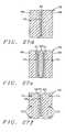
- the final two processing steps of the invention, before the solder metal is reflowed,are shown in the cross section of FIGS. 13 and 14 and affect the etching of the exposed surface of the barrier layer 36 .
- isotropic etchingthe exposed barrier layer is completely removed as is shown in FIG. 13 .
- anisotropic etchingin FIG. 14 , the etching of the barrier layer is partially impeded by the presence of the columns 42 of solder metal.
- the undercut shape of pillar 38will prevent wetting of pillar 38 and the UBM layer 40 during subsequent solder reflow. It is also believed that exposure to air will oxidize the sidewalls of pillar 38 and UBM layer 40 and therefore prevent wetting of these surfaces during subsequent solder reflow.
- the sidewalls of pillar 38 and UBM layer 40may be further oxidized by, for example, a thermal oxidation below reflow temperature of about 240 degrees C. such as heating in oxygen ambient at about 125 degrees C.
- FIGS. 15 and 16show the final cross section of the solder bump of the invention after the solder metal has been reflowed.
- FIG. 15corresponds to FIG. 13 while FIG. 16 corresponds to FIG. 14 , this relating to the etch in the barrier layer 36 that has been explained using FIGS. 13 and 14 .
- the etched layer 36 of barrier material that is shown in cross section in FIG. 15corresponds to the etched layer of barrier material that is shown in FIG. 13 .
- FIGS. 16 and 14show the same correspondence exists between FIGS. 16 and 14 .
- FIG. 17there is shown a cross section of the BGA package of the invention whereby the semiconductor device has been encapsulated in a molding compound.
- the elements that are highlighted in the cross section of FIG. 5are the following:
- the columns 54 of pillar metaltypically have a height of between about 10 and 100 ⁇ m and more preferably about 50 ⁇ m.
- FIG. 18The cross section that is shown in FIG. 18 is identical to the cross section of FIG. 17 with the exception of the underfill 62 which is used instead of the molding compound 60 of FIG. 17 .
- the creation of the pillar metal 54 and the solder bump 56starts using the I/O contact pads of device 50 (not shown in FIGS. 17 , 18 ) as the contact pads; that is the I/O contact pads of device 50 take the place of the contact pad 32 of FIGS. 15 and 16 in the creation of the pillar metal 54 and the solder bump 56 .
- the process of creating the pillar metal 54 and the solder bump 56therefore is as follows:
- FIG. 19there is shown a top view of an array type arrangement of I/O contact points 66 that form the contact points of device 50 .
- This top view of the array type contact points 66is shown as one example of where the process of creating pillar metal and solder bumps can be applied.
- FIGS. 20 and 21show two more examples of arrangements of I/O contact pads that are provided on the surface of device 50 , where the process of the invention can be applied.
- FIG. 20shows a peripheral I/O pad design 68 while
- FIG. 21shows a center type pad design 70 .
- peripheral I/O pad designthat is shown in FIG. 20 provides evenly distributed mechanical support for device 50 , this is not the case for the center pad design that is shown in FIG. 21 .
- additional mechanical supportcan be provided to device 50 ; this is shown in top view in FIG. 22 .
- the elements highlighted as 70 in FIG. 22are the solder bumps that have been created on the I/O contact pads of device 50 ; elements 72 are dummy solder bumps that can be provided in order to lend mechanical support to device 50 .
- the symmetry of the dummy bumps 72 as shown in FIG. 22makes clear that device 50 is, with the dummy bumps 72 , adequately and symmetrically supported.
- solder fluxIn mounting semiconductor devices on the surface of a BGA substrate, it is important from a manufacturing point of view that solder flux, after the process of solder flow has been completed, can be readily removed. This requires easy access to the surface areas of the BGA substrate where solder flux has been able to accumulate.
- the device interconnectsConsisting of pillar metal and solder bumps
- the flux that has accumulated in the gap between the semiconductor die and the substratemust be cleaned.
- solder masknot across the entire surface of the substrate (blank deposition) but to leave open the surface areas of the substrate that are immediately adjacent to the I/O interconnects (of pillar metal and solder bumps).
- This designwill create a channel though which the cleaning solution can flow easily. This is highlighted in the top view of FIGS. 23 and 24 , where is shown:
- FIGS. 25 and 26show how prior art procedures and conventions are applied to affect flux removal and encapsulant application.
- the metal pads 74are typically surrounded by the solder mask 78 , even for small pitch I/O pad designs.
- the solder maskis determined by the type of contact pad design ( FIGS. 19 through 21 ), whereby the contact pads 74 require about 60 ⁇ m clearance for reasons of proper alignment registration. This results in the substrate design rule being more critical, allowing for less error and smaller tolerance in the design parameters.
- the height of the solder mask 78is generally about 10 ⁇ m larger than the height of the contact pad 74 , further forming an obstacle in applying molding compound or in removing flux after the solder process has been completed.
- FIGS. 27 a through 27 fshow examples of applications of the invention, as follows:
- FIG. 27 ashows the application of a solder mask over the surface that has previously been shown in FIG. 19 , the solder mask has been indicated with cross-hatched regions 90 , the regions where no solder mask is present have been highlighted with 91 .
- FIGS. 27 b and 27 crelate to the previous FIG. 20 , the solder mask has been highlighted as regions 90 while the regions where no solder mask is present have been highlighted with 91 .
- the design that is shown in FIG. 27 cis considered a “partial” peripheral type I/O pad configuration of a semiconductor device since I/O pads 68 are only provided along two opposing sides of the semiconductor device 50 .
- FIGS. 27 b and 27 ccan further be provided with supporting dummy solder bumps in the regions of the solder mask 90 , these supporting solder bumps have not been shown in FIGS. 27 b and 27 c.
- FIG. 27 dshows the design that has previously been shown in FIG. 21
- FIG. 27 eshows a design that is similar to the design of FIG. 27 d with the exception that the contact points 70 have now been provided in two columns. It is clear from these two drawings that channels have been created in the solder mask that are in line with and include the contact pads. These channels allow for easy flow of cleaning fluid and therefore allow for easy removal of solder flux after the process of chip encapsulation and solder flow has been completed.
- FIG. 27 frelates to the previously shown FIG. 22 , the above observation relating to the creation of a channel through the solder flux and the therefrom following easy flow of cleaning fluid equally applies to the design that is shown in FIG. 27 f.
- FIGS. 28 a and 28 bdemonstrate how the invention leads to the ability to reduce the pitch between I/O pads.
- FIG. 28 ashows how in prior art applications the solder mask 90 is provided, further shown in FIG. 28 a are:
- the required clearanceis needed by the solder mask and requires that extra space is required between the circumference 95 of the contact pad and the circumference 94 of the opening created in the solder mask.
Landscapes
- Engineering & Computer Science (AREA)
- Computer Hardware Design (AREA)
- Microelectronics & Electronic Packaging (AREA)
- Power Engineering (AREA)
- Physics & Mathematics (AREA)
- Condensed Matter Physics & Semiconductors (AREA)
- General Physics & Mathematics (AREA)
- Internal Circuitry In Semiconductor Integrated Circuit Devices (AREA)
- Wire Bonding (AREA)
Abstract
Description
- 10, a semiconductor surface such as the surface of a substrate
- 30, a layer of dielectric that has been deposited over the
semiconductor surface 10 - 32, contact pads that have been created on the surface of the
layer 30 of dielectric - 34, a patterned layer of passivation that has been deposited over the surface of the
layer 30 of dielectric; openings have been created in thelayer 34 of passivation, partially exposing the surface ofcontact pads 32 - 36, an isotropically etched layer of barrier metal; this layer of barrier metal has been isotropically etched; that is, the barrier metal has been completely removed from the surface of the
layer 34 of passivation except where the barrier metal is covered by the overlying pillar metal (38) of the solder bump - 38, the pillar metal of the solder bump
- 40, a layer of under bump metal created overlying the
pillar metal 38 of the solder bump, wherein the distance between an edge of the under bump metal layer and an edge of the metal pillar of the solder bump is greater than 0.2 microns - 42, the solder metal.
- 10, a silicon substrate over the surface of which
metal contact pads 32 have been created - 30, a layer of dielectric that has been deposited over the surface of
substrate 10 - 32, the metal contact pads, typically comprising aluminum, created over the surface of the
layer 30 of dielectric - 34, a layer of passivation that has been deposited over the surface of the
layer 30 of dielectric. Openings have been created in thelayer 34 of passivation that align with themetal contact pads 32, partially exposing the surface of thecontact pads 32 - 36, a layer of barrier metal that has been created over the surface of
layer 34 of passivation, including the openings that have been created in thelayer 34 of passivation, contacting theunderlying contact pads 32.
- 10, a silicon substrate over the surface of which
- prior to and in preparation for the invention, a semiconductor surface is provided, a layer of dielectric has been deposited over the semiconductor surface, a contact pad has been provided on the layer of dielectric, the contact pad has an exposed surface, a layer of passivation has been deposited over a semiconductor surface including the surface of said contact pad, and the layer of passivation has been patterned and etched, creating an opening in the layer of passivation, partially exposing the surface of the contact pad, the opening in the layer of passivation is centered with respect to the contact pad
- the invention starts with a barrier layer deposited over the surface of the layer of passivation, making contact with the contact pad through the opening created in the layer of passivation
- a layer of photoresist is deposited over the surface of the barrier layer
- the layer of photoresist is patterned and etched, creating an opening through the layer of photoresist, wherein the opening in the layer of photoresist aligns with and is centered with respect to the contact pad
- in sequence are deposited, bounded by the opening created in the layer of photoresist, a layer of pillar metal, a layer of under bump metal and a layer of solder metal
- the patterned layer of photoresist is removed from the surface of the barrier layer
- the layer of pillar metal is etched, reducing the diameter of the pillar metal
- the barrier layer is etched, using either isotropic or anisotropic etching
- the solder metal is reflowed.
- ball height is a very important reliability concern; in order to prevent thermal mismatch between overlying layers of a package (such as a semiconductor device and an underlying printed circuit board and the like) it is important to increase the distance between overlying elements; the invention provides this ability
- a larger solder ball (for better thermal or reliability performance) results in increased pitch; this is contrary to state of the art design requirements
- if small solder balls are used without providing height, it is very difficult to underfill the small gaps
- the solder is, using the invention, relatively far removed from the semiconductor device which means that the application of low-alpha solder is not required (alpha-particles create soft errors in memory products; lead is known to emit alpha-particles when lead decays)
- for the pillar metal a metal needs to be selected that has good conductivity and good ductility, such as copper. This is in order to provide improved thermal performance by counteracting thermal stress
- the height of the pillar of the solder bump of the invention is important and should be between about 10 to 100 μm in order to achieve objectives of high stand-off
- the metal that is used for the under bump metal layer is important in that this metal must have good adhesion with the overlying solder during solder reflow while this metal must not solve too fast and in so doing form a barrier to the solder; in addition, the UBM metal when exposed to air can form a layer of protective oxide thus preventing solder wetting to the pillar metal around the perimeter of the UBM metal during the reflow process; nickel is therefore preferred for the UBM metal
- 50, a semiconductor device that is mounted in the package of the invention shown in cross section in
FIG. 17 - 52, the (BGA) substrate on the surface of which
device 50 is mounted - 54, the pillar metal of the interface between the
device 50 and theBGA substrate 52, similar topillar metal 38 ofFIGS. 15 and 16 - 56, the solder bump of the interface between the
device 50 and theBGA substrate 52, similar tosolder bump 42 ofFIGS. 15 and 16 - 58, the contact balls that are used to interconnect the package of the invention with surrounding circuitry
- 60, molding compound into which the
device 50 is embedded for protection against the environment.
- 50, a semiconductor device that is mounted in the package of the invention shown in cross section in
- a layer of dielectric is deposited over the active surface of
device 50; the active surface ofdevice 50 is the surface in which I/O contact points have been provided; this surface will face theBGA substrate 52 after mounting of thedevice 50 onBGA substrate 52 - openings are created in the layer of dielectric, exposing the I/O contact pads of
device 50; this brings the process of the invention to the point of the related application where contact pads32 (FIGS. 15 ,16) have been created on the surface of thelayer 30 of dielectric - a layer of passivation is deposited over the surface of the layer of dielectric, similar to
layer 34,FIGS. 15 ,16 - openings are created in the layer of passivation, partially exposing the surface of the device I/O contact pads
- a barrier layer is deposited over the surface of the layer of passivation, identical to
layer 36,FIGS. 15 ,16 - the
pillar metal 54 of the solder bump is formed, identical tolayer 38,FIGS. 15 ,16 - the layer of under bump (not shown in
FIGS. 17 ,18) is created overlying the pillar metal, identical tolayer 40,FIGS. 15 ,16 - the
solder bump 56 is formed, identical tolayer 42,FIGS. 15 ,16 - the layer of barrier metal is isotropically (
FIG. 15 ) or anisotropically (FIG. 16 ) etched.
- a layer of dielectric is deposited over the active surface of
- 52, the BGA substrate on the surface of which device50 (not shown) is mounted
- 74, I/O contact pads provided on the surface of
substrate 52 - 76, interconnect traces provided on the surface of
substrate 52, connected withcontact pads 74 - 79, the surface region of the
substrate 52 over which no solder mask is applied - 80, the surface region of the
substrate 52 over which a solder mask is applied.
- 94, the circumference of the opening that is created in the
solder mask 90 - 95, the circumference of the bond pad on the surface of a semiconductor device
- 92, the distance (or spacing) S between two adjacent contact pads
- 93, the diameter D of a contact pad.
- 94, the circumference of the opening that is created in the
Claims (20)
Priority Applications (1)
| Application Number | Priority Date | Filing Date | Title |
|---|---|---|---|
| US11/981,138US7902679B2 (en) | 2001-03-05 | 2007-10-31 | Structure and manufacturing method of a chip scale package with low fabrication cost, fine pitch and high reliability solder bump |
Applications Claiming Priority (3)
| Application Number | Priority Date | Filing Date | Title |
|---|---|---|---|
| US09/798,654US6818545B2 (en) | 2001-03-05 | 2001-03-05 | Low fabrication cost, fine pitch and high reliability solder bump |
| US83700701A | 2001-04-18 | 2001-04-18 | |
| US11/981,138US7902679B2 (en) | 2001-03-05 | 2007-10-31 | Structure and manufacturing method of a chip scale package with low fabrication cost, fine pitch and high reliability solder bump |
Related Parent Applications (1)
| Application Number | Title | Priority Date | Filing Date |
|---|---|---|---|
| US83700701AContinuation | 2001-03-05 | 2001-04-18 |
Publications (2)
| Publication Number | Publication Date |
|---|---|
| US20080067677A1 US20080067677A1 (en) | 2008-03-20 |
| US7902679B2true US7902679B2 (en) | 2011-03-08 |
Family
ID=39187738
Family Applications (5)
| Application Number | Title | Priority Date | Filing Date |
|---|---|---|---|
| US11/981,138Expired - Fee RelatedUS7902679B2 (en) | 2001-03-05 | 2007-10-31 | Structure and manufacturing method of a chip scale package with low fabrication cost, fine pitch and high reliability solder bump |
| US11/981,125Expired - Fee RelatedUS8158508B2 (en) | 2001-03-05 | 2007-10-31 | Structure and manufacturing method of a chip scale package |
| US12/384,977AbandonedUS20090267213A1 (en) | 2001-03-05 | 2009-04-09 | Structure and manufacturing method of a chip scale package with low fabrication cost, fine pitch and high reliability solder bump |
| US12/852,467AbandonedUS20110024905A1 (en) | 2001-03-05 | 2010-08-07 | Structure and manufacturing method of a chip scale package with low fabrication cost, fine pitch and high reliability solder bump |
| US12/852,470AbandonedUS20110024902A1 (en) | 2001-03-05 | 2010-08-07 | Structure and manufacturing method of a chip scale package with low fabrication cost, fine pitch and high reliability solder bump |
Family Applications After (4)
| Application Number | Title | Priority Date | Filing Date |
|---|---|---|---|
| US11/981,125Expired - Fee RelatedUS8158508B2 (en) | 2001-03-05 | 2007-10-31 | Structure and manufacturing method of a chip scale package |
| US12/384,977AbandonedUS20090267213A1 (en) | 2001-03-05 | 2009-04-09 | Structure and manufacturing method of a chip scale package with low fabrication cost, fine pitch and high reliability solder bump |
| US12/852,467AbandonedUS20110024905A1 (en) | 2001-03-05 | 2010-08-07 | Structure and manufacturing method of a chip scale package with low fabrication cost, fine pitch and high reliability solder bump |
| US12/852,470AbandonedUS20110024902A1 (en) | 2001-03-05 | 2010-08-07 | Structure and manufacturing method of a chip scale package with low fabrication cost, fine pitch and high reliability solder bump |
Country Status (1)
| Country | Link |
|---|---|
| US (5) | US7902679B2 (en) |
Cited By (50)
| Publication number | Priority date | Publication date | Assignee | Title |
|---|---|---|---|---|
| US20090160049A1 (en)* | 2006-12-25 | 2009-06-25 | Rohm Co., Ltd. | Semiconductor device |
| US20090184419A1 (en)* | 2005-05-16 | 2009-07-23 | Stats Chippac, Ltd. | Flip Chip Interconnect Solder Mask |
| US20090206493A1 (en)* | 2003-11-08 | 2009-08-20 | Stats Chippac, Ltd. | Flip Chip Interconnection Pad Layout |
| US20100065966A1 (en)* | 2006-12-14 | 2010-03-18 | Stats Chippac, Ltd. | Solder Joint Flip Chip Interconnection |
| US20100099222A1 (en)* | 2006-12-14 | 2010-04-22 | Stats Chippac, Ltd. | Solder Joint Flip Chip Interconnection Having Relief Structure |
| US20100117230A1 (en)* | 2008-04-03 | 2010-05-13 | Stats Chippac, Ltd. | Flip Chip Interconnection Structure Having Void-Free Fine Pitch and Method Thereof |
| US20100164097A1 (en)* | 2008-12-31 | 2010-07-01 | Stats Chippac, Ltd. | Semiconductor Device and Method of Confining Conductive Bump Material During Reflow with Solder Mask Patch |
| US20100176510A1 (en)* | 2006-09-22 | 2010-07-15 | Stats Chippac, Inc. | Fusible I/O Interconnection Systems and Methods for Flip-Chip Packaging Involving Substrate-Mounted Stud Bumps |
| US20100193947A1 (en)* | 2005-03-25 | 2010-08-05 | Stats Chippac, Ltd. | Flip Chip Interconnection Having Narrow Interconnection Sites on the Substrate |
| US20100237500A1 (en)* | 2009-03-20 | 2010-09-23 | Stats Chippac, Ltd. | Semiconductor Substrate and Method of Forming Conformal Solder Wet-Enhancement Layer on Bump-on-Lead Site |
| US20100237484A1 (en)* | 2009-03-19 | 2010-09-23 | Samsung Electronics Co., Ltd. | Semiconductor package |
| US20100244245A1 (en)* | 2008-03-25 | 2010-09-30 | Stats Chippac, Ltd. | Filp Chip Interconnection Structure with Bump on Partial Pad and Method Thereof |
| US20100246150A1 (en)* | 2007-11-06 | 2010-09-30 | Agency For Science Tecnology And Research | Interconnect Structure And A Method Of Fabricating The Same |
| US20100276787A1 (en)* | 2009-04-30 | 2010-11-04 | Taiwan Semiconductor Manufacturing Company, Ltd. | Wafer Backside Structures Having Copper Pillars |
| US20110049706A1 (en)* | 2009-09-03 | 2011-03-03 | Taiwan Semiconductor Manufacturing Company, Ltd. | Front Side Copper Post Joint Structure for Temporary Bond in TSV Application |
| US20110074022A1 (en)* | 2000-03-10 | 2011-03-31 | Stats Chippac, Ltd. | Semiconductor Device and Method of Forming Flipchip Interconnect Structure |
| US20110074024A1 (en)* | 2003-11-10 | 2011-03-31 | Stats Chippac, Ltd. | Semiconductor Device and Method of Forming Bump-on-Lead Interconnection |
| US20110074026A1 (en)* | 2008-03-19 | 2011-03-31 | Stats Chippac, Ltd. | Semiconductor Device and Method of Forming Insulating Layer on Conductive Traces for Electrical Isolation in Fine Pitch Bonding |
| US20110122592A1 (en)* | 2009-11-24 | 2011-05-26 | Sanka Ganesan | First-level interconnects with slender columns, and processes of forming same |
| US20110121452A1 (en)* | 2008-09-10 | 2011-05-26 | Stats Chippac, Ltd. | Semiconductor Device Having Vertically Offset Bond on Trace Interconnects on Recessed and Raised Bond Fingers |
| US20110133334A1 (en)* | 2008-12-31 | 2011-06-09 | Stats Chippac, Ltd. | Semiconductor Device and Method of Confining Conductive Bump Material with Solder Mask Patch |
| US20110215468A1 (en)* | 2003-11-10 | 2011-09-08 | Stats Chippac, Ltd. | Bump-on-Lead Flip Chip Interconnection |
| US20110215476A1 (en)* | 2002-01-07 | 2011-09-08 | Megica Corporation | Method for fabricating circuit component |
| US20120056320A1 (en)* | 2010-09-03 | 2012-03-08 | Kabushiki Kaisha Toshiba | Semiconductor device and manufacturing method of semiconductor device |
| US20120267779A1 (en)* | 2011-04-25 | 2012-10-25 | Mediatek Inc. | Semiconductor package |
| US20120295434A1 (en)* | 2011-05-18 | 2012-11-22 | Samsung Electronics Co., Ltd | Solder collapse free bumping process of semiconductor device |
| US8350384B2 (en) | 2009-11-24 | 2013-01-08 | Stats Chippac, Ltd. | Semiconductor device and method of forming electrical interconnect with stress relief void |
| US8409978B2 (en) | 2010-06-24 | 2013-04-02 | Stats Chippac, Ltd. | Semiconductor device and method of forming vertically offset bond on trace interconnect structure on leadframe |
| US8435834B2 (en) | 2010-09-13 | 2013-05-07 | Stats Chippac, Ltd. | Semiconductor device and method of forming bond-on-lead interconnection for mounting semiconductor die in FO-WLCSP |
| US8461045B2 (en) | 2008-10-09 | 2013-06-11 | Taiwan Semiconductor Manufacturing Company, Ltd. | Bond pad connection to redistribution lines having tapered profiles |
| US8492197B2 (en) | 2010-08-17 | 2013-07-23 | Stats Chippac, Ltd. | Semiconductor device and method of forming vertically offset conductive pillars over first substrate aligned to vertically offset BOT interconnect sites formed over second substrate |
| USRE44500E1 (en) | 2003-11-10 | 2013-09-17 | Stats Chippac, Ltd. | Semiconductor device and method of forming composite bump-on-lead interconnection |
| US8563418B2 (en) | 2010-03-09 | 2013-10-22 | Stats Chippac, Ltd. | Semiconductor device and method of forming vertically offset bond on trace interconnects on different height traces |
| USRE44562E1 (en) | 2003-11-10 | 2013-10-29 | Stats Chippac, Ltd. | Solder joint flip chip interconnection having relief structure |
| USRE44579E1 (en) | 2003-11-10 | 2013-11-05 | Stats Chippac, Ltd. | Semiconductor device and method of self-confinement of conductive bump material during reflow without solder mask |
| USRE44608E1 (en) | 2003-11-10 | 2013-11-26 | Stats Chippac, Ltd. | Solder joint flip chip interconnection |
| US8659153B2 (en) | 2012-07-16 | 2014-02-25 | Micron Technology, Inc. | Pillar on pad interconnect structures, semiconductor dice and die assemblies including such interconnect structures, and related methods |
| US8759972B2 (en) | 2003-11-10 | 2014-06-24 | Stats Chippac, Ltd. | Semiconductor device and method of forming composite bump-on-lead interconnection |
| US8841779B2 (en) | 2005-03-25 | 2014-09-23 | Stats Chippac, Ltd. | Semiconductor device and method of forming high routing density BOL BONL and BONP interconnect sites on substrate |
| US9029196B2 (en) | 2003-11-10 | 2015-05-12 | Stats Chippac, Ltd. | Semiconductor device and method of self-confinement of conductive bump material during reflow without solder mask |
| US9258904B2 (en) | 2005-05-16 | 2016-02-09 | Stats Chippac, Ltd. | Semiconductor device and method of forming narrow interconnect sites on substrate with elongated mask openings |
| US9345148B2 (en) | 2008-03-25 | 2016-05-17 | Stats Chippac, Ltd. | Semiconductor device and method of forming flipchip interconnection structure with bump on partial pad |
| US20170033066A1 (en)* | 2013-11-01 | 2017-02-02 | Infineon Technologies Ag | Semiconductor Devices and Methods of Forming Thereof |
| US9780057B2 (en) | 2003-11-08 | 2017-10-03 | STATS ChipPAC Pte. Ltd. | Semiconductor device and method of forming pad layout for flipchip semiconductor die |
| US9847309B2 (en) | 2006-09-22 | 2017-12-19 | STATS ChipPAC Pte. Ltd. | Semiconductor device and method of forming vertical interconnect structure between semiconductor die and substrate |
| US10037938B2 (en) | 2016-10-31 | 2018-07-31 | Samsung Electronics Co., Ltd. | Semiconductor packages |
| USRE47600E1 (en) | 2003-11-10 | 2019-09-10 | STATS ChipPAC Pte. Ltd. | Semiconductor device and method of forming electrical interconnect with stress relief void |
| US10636758B2 (en)* | 2017-10-05 | 2020-04-28 | Texas Instruments Incorporated | Expanded head pillar for bump bonds |
| US11276658B2 (en)* | 2018-06-20 | 2022-03-15 | Micron Technology, Inc. | Devices with three-dimensional structures and support elements to increase adhesion to substrates |
| US20220328394A1 (en)* | 2021-04-07 | 2022-10-13 | Mediatek Inc. | Three-dimensional pad structure and interconnection structure for electronic devices |
Families Citing this family (62)
| Publication number | Priority date | Publication date | Assignee | Title |
|---|---|---|---|---|
| US9084377B2 (en)* | 2007-03-30 | 2015-07-14 | Stats Chippac Ltd. | Integrated circuit package system with mounting features for clearance |
| JP5200837B2 (en)* | 2008-10-01 | 2013-06-05 | 富士通セミコンダクター株式会社 | Manufacturing method of semiconductor device |
| JP2010166025A (en)* | 2008-12-19 | 2010-07-29 | Panasonic Corp | Mounting structure |
| CN102265716B (en) | 2008-12-26 | 2015-04-01 | 高通股份有限公司 | Chip packaging with power management integrated circuits and related technologies |
| US8169058B2 (en)* | 2009-08-21 | 2012-05-01 | Stats Chippac, Ltd. | Semiconductor device and method of stacking die on leadframe electrically connected by conductive pillars |
| USRE48111E1 (en) | 2009-08-21 | 2020-07-21 | JCET Semiconductor (Shaoxing) Co. Ltd. | Semiconductor device and method of forming interposer frame over semiconductor die to provide vertical interconnect |
| US8383457B2 (en) | 2010-09-03 | 2013-02-26 | Stats Chippac, Ltd. | Semiconductor device and method of forming interposer frame over semiconductor die to provide vertical interconnect |
| US8227926B2 (en)* | 2009-10-23 | 2012-07-24 | Ati Technologies Ulc | Routing layer for mitigating stress in a semiconductor die |
| US8299632B2 (en) | 2009-10-23 | 2012-10-30 | Ati Technologies Ulc | Routing layer for mitigating stress in a semiconductor die |
| US20110133327A1 (en)* | 2009-12-09 | 2011-06-09 | Hung-Hsin Hsu | Semiconductor package of metal post solder-chip connection |
| US8884422B2 (en) | 2009-12-31 | 2014-11-11 | Stmicroelectronics Pte Ltd. | Flip-chip fan-out wafer level package for package-on-package applications, and method of manufacture |
| US20110156240A1 (en)* | 2009-12-31 | 2011-06-30 | Stmicroelectronics Asia Pacific Pte. Ltd. | Reliable large die fan-out wafer level package and method of manufacture |
| US8502394B2 (en)* | 2009-12-31 | 2013-08-06 | Stmicroelectronics Pte Ltd. | Multi-stacked semiconductor dice scale package structure and method of manufacturing same |
| US8466997B2 (en) | 2009-12-31 | 2013-06-18 | Stmicroelectronics Pte Ltd. | Fan-out wafer level package for an optical sensor and method of manufacture thereof |
| US20110169158A1 (en)* | 2010-01-14 | 2011-07-14 | Qualcomm Incorporated | Solder Pillars in Flip Chip Assembly |
| TWI502696B (en)* | 2010-02-06 | 2015-10-01 | Ind Tech Res Inst | Bonding structure and method of fabricating the same |
| US20110193212A1 (en)* | 2010-02-08 | 2011-08-11 | Qualcomm Incorporated | Systems and Methods Providing Arrangements of Vias |
| KR101630394B1 (en)* | 2010-03-08 | 2016-06-24 | 삼성전자주식회사 | Package substrate, semiconductor package comprising the same and method for fabricating the semiconductor package |
| US8759209B2 (en)* | 2010-03-25 | 2014-06-24 | Stats Chippac, Ltd. | Semiconductor device and method of forming a dual UBM structure for lead free bump connections |
| KR20110124993A (en)* | 2010-05-12 | 2011-11-18 | 삼성전자주식회사 | Semiconductor chip, semiconductor package and method for manufacturing same |
| US9142533B2 (en) | 2010-05-20 | 2015-09-22 | Taiwan Semiconductor Manufacturing Company, Ltd. | Substrate interconnections having different sizes |
| JP5310947B2 (en)* | 2010-06-02 | 2013-10-09 | 株式会社村田製作所 | ESD protection device |
| JP5539077B2 (en)* | 2010-07-09 | 2014-07-02 | ローム株式会社 | Semiconductor device |
| TWI478303B (en) | 2010-09-27 | 2015-03-21 | Advanced Semiconductor Eng | Chip having metal pillar and package having the same |
| CN102148215B (en)* | 2011-01-21 | 2012-06-06 | 哈尔滨理工大学 | Interconnection structure for improving reliability of soldering spot of soft soldering of CCGA (Ceramic Column Grid Array) device and implementation method |
| US8435881B2 (en) | 2011-06-23 | 2013-05-07 | STAT ChipPAC, Ltd. | Semiconductor device and method of forming protective coating over interconnect structure to inhibit surface oxidation |
| US9013037B2 (en)* | 2011-09-14 | 2015-04-21 | Stmicroelectronics Pte Ltd. | Semiconductor package with improved pillar bump process and structure |
| US8581400B2 (en) | 2011-10-13 | 2013-11-12 | Taiwan Semiconductor Manufacturing Company, Ltd. | Post-passivation interconnect structure |
| US8916481B2 (en) | 2011-11-02 | 2014-12-23 | Stmicroelectronics Pte Ltd. | Embedded wafer level package for 3D and package-on-package applications, and method of manufacture |
| US8779601B2 (en) | 2011-11-02 | 2014-07-15 | Stmicroelectronics Pte Ltd | Embedded wafer level package for 3D and package-on-package applications, and method of manufacture |
| US9613917B2 (en) | 2012-03-30 | 2017-04-04 | Taiwan Semiconductor Manufacturing Company, Ltd. | Package-on-package (PoP) device with integrated passive device in a via |
| US9425136B2 (en) | 2012-04-17 | 2016-08-23 | Taiwan Semiconductor Manufacturing Company, Ltd. | Conical-shaped or tier-shaped pillar connections |
| US9299674B2 (en) | 2012-04-18 | 2016-03-29 | Taiwan Semiconductor Manufacturing Company, Ltd. | Bump-on-trace interconnect |
| KR102007780B1 (en)* | 2012-07-31 | 2019-10-21 | 삼성전자주식회사 | Methods for fabricating semiconductor devices having multi-bump structural electrical interconnections |
| US9165887B2 (en) | 2012-09-10 | 2015-10-20 | Taiwan Semiconductor Manufacturing Company, Ltd. | Semiconductor device with discrete blocks |
| US9607862B2 (en)* | 2012-09-11 | 2017-03-28 | Globalfoundries Inc. | Extrusion-resistant solder interconnect structures and methods of forming |
| US9111817B2 (en) | 2012-09-18 | 2015-08-18 | Taiwan Semiconductor Manufacturing Company, Ltd. | Bump structure and method of forming same |
| US8975726B2 (en) | 2012-10-11 | 2015-03-10 | Taiwan Semiconductor Manufacturing Company, Ltd. | POP structures and methods of forming the same |
| US9391041B2 (en) | 2012-10-19 | 2016-07-12 | Taiwan Semiconductor Manufacturing Company, Ltd. | Fan-out wafer level package structure |
| US8847412B2 (en) | 2012-11-09 | 2014-09-30 | Invensas Corporation | Microelectronic assembly with thermally and electrically conductive underfill |
| TWI473227B (en)* | 2012-11-15 | 2015-02-11 | 矽品精密工業股份有限公司 | Connecting structure for substrate and method of forming same |
| US9245770B2 (en)* | 2012-12-20 | 2016-01-26 | Stats Chippac, Ltd. | Semiconductor device and method of simultaneous molding and thermalcompression bonding |
| US9881889B2 (en)* | 2013-04-12 | 2018-01-30 | Xintec Inc. | Chip package and method for fabricating the same |
| US9559071B2 (en)* | 2013-06-26 | 2017-01-31 | Taiwan Semiconductor Manufacturing Company, Ltd. | Mechanisms for forming hybrid bonding structures with elongated bumps |
| US9679839B2 (en) | 2013-10-30 | 2017-06-13 | Taiwan Semiconductor Manufacturing Company, Ltd. | Chip on package structure and method |
| US9373527B2 (en) | 2013-10-30 | 2016-06-21 | Taiwan Semiconductor Manufacturing Company, Ltd. | Chip on package structure and method |
| US9449947B2 (en)* | 2014-07-01 | 2016-09-20 | Taiwan Semiconductor Manufacturing Company, Ltd. | Semiconductor package for thermal dissipation |
| US9633965B2 (en)* | 2014-08-08 | 2017-04-25 | Taiwan Semiconductor Manufacturing Company Ltd. | Semiconductor structure and manufacturing method of the same |
| US9564410B2 (en)* | 2015-07-08 | 2017-02-07 | Texas Instruments Incorporated | Semiconductor devices having metal bumps with flange |
| JP6253622B2 (en)* | 2015-09-08 | 2017-12-27 | キヤノン株式会社 | Liquid crystal drive device, image display device, and liquid crystal drive program |
| US9899239B2 (en)* | 2015-11-06 | 2018-02-20 | Apple Inc. | Carrier ultra thin substrate |
| US10593084B2 (en)* | 2016-08-01 | 2020-03-17 | Facebook, Inc. | Systems and methods for content interaction |
| US20190259731A1 (en)* | 2016-11-09 | 2019-08-22 | Unisem (M) Berhad | Substrate based fan-out wafer level packaging |
| CN110165442B (en)* | 2018-02-12 | 2020-11-03 | 泰达电子股份有限公司 | Metal Block Welding Column Combination and Its Application Power Module |
| CN110324956B (en)* | 2018-03-30 | 2022-05-20 | 广州市信宏洗衣机械有限公司 | Heat radiator for multilayer circuit board |
| DE102019103355A1 (en) | 2019-02-11 | 2020-08-13 | Infineon Technologies Ag | A semiconductor device having a copper pillar interconnection structure |
| TWI692064B (en)* | 2019-06-06 | 2020-04-21 | 力成科技股份有限公司 | Semiconductor chip having coplanar bumps and manufacturing method thereof |
| US11721657B2 (en) | 2019-06-14 | 2023-08-08 | Stmicroelectronics Pte Ltd | Wafer level chip scale package having varying thicknesses |
| US11199673B2 (en)* | 2019-07-31 | 2021-12-14 | Hewlett Packard Enterprise Development Lp | Optoelectronic device with integrated underfill exclusion structure |
| US11056443B2 (en) | 2019-08-29 | 2021-07-06 | Micron Technology, Inc. | Apparatuses exhibiting enhanced stress resistance and planarity, and related methods |
| US12261102B2 (en)* | 2021-08-30 | 2025-03-25 | Taiwan Semiconductor Manufacturing Company, Ltd. | Semiconductor package and method of forming the same |
| WO2023177417A1 (en)* | 2022-03-18 | 2023-09-21 | Celestial Ai Inc. | Photonic fabric with optical interface for connection to memory |
Citations (162)
| Publication number | Priority date | Publication date | Assignee | Title |
|---|---|---|---|---|
| US4087314A (en) | 1976-09-13 | 1978-05-02 | Motorola, Inc. | Bonding pedestals for semiconductor devices |
| US4179802A (en) | 1978-03-27 | 1979-12-25 | International Business Machines Corporation | Studded chip attachment process |
| US4652336A (en) | 1984-09-20 | 1987-03-24 | Siemens Aktiengesellschaft | Method of producing copper platforms for integrated circuits |
| US4685998A (en) | 1984-03-22 | 1987-08-11 | Thomson Components - Mostek Corp. | Process of forming integrated circuits with contact pads in a standard array |
| US5046161A (en) | 1988-02-23 | 1991-09-03 | Nec Corporation | Flip chip type semiconductor device |
| US5061985A (en) | 1988-06-13 | 1991-10-29 | Hitachi, Ltd. | Semiconductor integrated circuit device and process for producing the same |
| US5071518A (en) | 1989-10-24 | 1991-12-10 | Microelectronics And Computer Technology Corporation | Method of making an electrical multilayer interconnect |
| US5083187A (en) | 1990-05-16 | 1992-01-21 | Texas Instruments Incorporated | Integrated circuit device having bumped power supply buses over active surface areas and method of manufacture thereof |
| US5108950A (en) | 1987-11-18 | 1992-04-28 | Casio Computer Co., Ltd. | Method for forming a bump electrode for a semiconductor device |
| US5132775A (en) | 1987-12-11 | 1992-07-21 | Texas Instruments Incorporated | Methods for and products having self-aligned conductive pillars on interconnects |
| US5172471A (en) | 1991-06-21 | 1992-12-22 | Vlsi Technology, Inc. | Method of providing power to an integrated circuit |
| US5226232A (en) | 1990-05-18 | 1993-07-13 | Hewlett-Packard Company | Method for forming a conductive pattern on an integrated circuit |
| US5244833A (en) | 1989-07-26 | 1993-09-14 | International Business Machines Corporation | Method for manufacturing an integrated circuit chip bump electrode using a polymer layer and a photoresist layer |
| US5251806A (en) | 1990-06-19 | 1993-10-12 | International Business Machines Corporation | Method of forming dual height solder interconnections |
| US5252781A (en) | 1991-05-31 | 1993-10-12 | International Business Machines Corporation | Substrate member having electric lines and apertured insulating film |
| US5261155A (en) | 1991-08-12 | 1993-11-16 | International Business Machines Corporation | Method for bonding flexible circuit to circuitized substrate to provide electrical connection therebetween using different solders |
| US5349495A (en) | 1989-06-23 | 1994-09-20 | Vlsi Technology, Inc. | System for securing and electrically connecting a semiconductor chip to a substrate |
| US5418186A (en) | 1993-07-15 | 1995-05-23 | Samsung Electronics Co., Ltd. | Method for manufacturing a bump on a semiconductor chip |
| US5439162A (en) | 1993-06-28 | 1995-08-08 | Motorola, Inc. | Direct chip attachment structure and method |
| US5468984A (en) | 1994-11-02 | 1995-11-21 | Texas Instruments Incorporated | ESD protection structure using LDMOS diodes with thick copper interconnect |
| US5508561A (en) | 1993-11-15 | 1996-04-16 | Nec Corporation | Apparatus for forming a double-bump structure used for flip-chip mounting |
| US5523920A (en) | 1994-01-03 | 1996-06-04 | Motorola, Inc. | Printed circuit board comprising elevated bond pads |
| US5532512A (en) | 1994-10-03 | 1996-07-02 | General Electric Company | Direct stacked and flip chip power semiconductor device structures |
| US5541135A (en) | 1995-05-30 | 1996-07-30 | Motorola, Inc. | Method of fabricating a flip chip semiconductor device having an inductor |
| US5554940A (en) | 1994-07-05 | 1996-09-10 | Motorola, Inc. | Bumped semiconductor device and method for probing the same |
| US5565379A (en) | 1993-01-29 | 1996-10-15 | Mitsubishi Denki Kabushiki Kaisha | Method of manufacturing a semiconductor device having a bump electrode by a proximity exposure method |
| US5567655A (en) | 1993-05-05 | 1996-10-22 | Lsi Logic Corporation | Method for forming interior bond pads having zig-zag linear arrangement |
| US5600180A (en) | 1994-07-22 | 1997-02-04 | Nec Corporation | Sealing structure for bumps on a semiconductor integrated circuit chip |
| US5633535A (en) | 1995-01-27 | 1997-05-27 | Chao; Clinton C. | Spacing control in electronic device assemblies |
| US5643830A (en) | 1993-05-05 | 1997-07-01 | Lsi Logic Corporation | Process for manufacturing off-axis power branches for interior bond pad arrangements |
| US5656858A (en) | 1994-10-19 | 1997-08-12 | Nippondenso Co., Ltd. | Semiconductor device with bump structure |
| US5656863A (en) | 1993-02-18 | 1997-08-12 | Mitsubishi Denki Kabushiki Kaisha | Resin seal semiconductor package |
| US5659201A (en) | 1995-06-05 | 1997-08-19 | Advanced Micro Devices, Inc. | High conductivity interconnection line |
| US5665639A (en) | 1994-02-23 | 1997-09-09 | Cypress Semiconductor Corp. | Process for manufacturing a semiconductor device bump electrode using a rapid thermal anneal |
| US5664642A (en) | 1996-08-26 | 1997-09-09 | Williams; Bernard | Fire evacuation kit |
| US5691248A (en) | 1995-07-26 | 1997-11-25 | International Business Machines Corporation | Methods for precise definition of integrated circuit chip edges |
| US5731223A (en) | 1996-09-24 | 1998-03-24 | Lsi Logic Corporation | Array of solder pads on an integrated circuit |
| US5741726A (en) | 1993-10-22 | 1998-04-21 | Lsi Logic Corporation | Semiconductor device assembly with minimized bond finger connections |
| US5744843A (en) | 1996-08-28 | 1998-04-28 | Texas Instruments Incorporated | CMOS power device and method of construction and layout |
| US5756370A (en) | 1996-02-08 | 1998-05-26 | Micron Technology, Inc. | Compliant contact system with alignment structure for testing unpackaged semiconductor dice |
| US5767010A (en) | 1995-03-20 | 1998-06-16 | Mcnc | Solder bump fabrication methods and structure including a titanium barrier layer |
| US5790377A (en)* | 1996-09-12 | 1998-08-04 | Packard Hughes Interconnect Company | Integral copper column with solder bump flip chip |
| US5792594A (en) | 1996-04-01 | 1998-08-11 | Motorola, Inc. | Metallization and termination process for an integrated circuit chip |
| JP2785338B2 (en) | 1989-06-19 | 1998-08-13 | 日本電気株式会社 | Method for manufacturing semiconductor device |
| US5796169A (en) | 1996-11-19 | 1998-08-18 | International Business Machines Corporation | Structurally reinforced ball grid array semiconductor package and systems |
| US5834849A (en) | 1996-02-13 | 1998-11-10 | Altera Corporation | High density integrated circuit pad structures |
| US5834844A (en) | 1995-03-24 | 1998-11-10 | Shinko Electric Industries Co., Ltd. | Semiconductor device having an element with circuit pattern thereon |
| US5844782A (en) | 1994-12-20 | 1998-12-01 | Sony Corporation | Printed wiring board and electronic device using same |
| US5854513A (en) | 1995-07-14 | 1998-12-29 | Lg Electronics Inc. | Semiconductor device having a bump structure and test electrode |
| US5872399A (en) | 1996-04-01 | 1999-02-16 | Anam Semiconductor, Inc. | Solder ball land metal structure of ball grid semiconductor package |
| US5870822A (en) | 1996-05-22 | 1999-02-16 | International Computers Limited | Flip chip attachment |
| US5883435A (en) | 1996-07-25 | 1999-03-16 | International Business Machines Corporation | Personalization structure for semiconductor devices |
| US5882957A (en) | 1997-06-09 | 1999-03-16 | Compeq Manufacturing Company Limited | Ball grid array packaging method for an integrated circuit and structure realized by the method |
| US5892273A (en) | 1994-10-03 | 1999-04-06 | Kabushiki Kaisha Toshiba | Semiconductor package integral with semiconductor chip |
| US5898222A (en) | 1995-05-12 | 1999-04-27 | International Business Machines Corporation | Capped copper electrical interconnects |
| US5931371A (en) | 1997-01-16 | 1999-08-03 | Ford Motor Company | Standoff controlled interconnection |
| US5943597A (en) | 1998-06-15 | 1999-08-24 | Motorola, Inc. | Bumped semiconductor device having a trench for stress relief |
| US6013571A (en) | 1997-06-16 | 2000-01-11 | Motorola, Inc. | Microelectronic assembly including columnar interconnections and method for forming same |
| US6015505A (en) | 1997-10-30 | 2000-01-18 | International Business Machines Corporation | Process improvements for titanium-tungsten etching in the presence of electroplated C4's |
| US6022792A (en) | 1996-03-13 | 2000-02-08 | Seiko Instruments, Inc. | Semiconductor dicing and assembling method |
| US6030512A (en) | 1997-03-31 | 2000-02-29 | Shinko Electric Industries, Co. Ltd. | Device for forming bumps by metal plating |
| US6042953A (en) | 1996-03-21 | 2000-03-28 | Matsushita Electric Industrial Co., Ltd. | Substrate on which bumps are formed and method of forming the same |
| JP2000106362A (en) | 1998-07-30 | 2000-04-11 | Motorola Inc | Production of electronic part |
| US6049122A (en) | 1997-10-16 | 2000-04-11 | Fujitsu Limited | Flip chip mounting substrate with resin filled between substrate and semiconductor chip |
| US6051450A (en) | 1997-07-01 | 2000-04-18 | Sony Corporation | Lead frame, manufacturing method of a lead frame, semiconductor device, assembling method of a semiconductor device, and electronic apparatus |
| US6060683A (en) | 1998-09-22 | 2000-05-09 | Direct Radiography Corp. | Selective laser removal of dielectric coating |
| EP1005082A1 (en) | 1998-03-27 | 2000-05-31 | Seiko Epson Corporation | Semiconductor device, method for manufacturing the same, circuit board and electronic apparatus |
| US6072236A (en) | 1996-03-07 | 2000-06-06 | Micron Technology, Inc. | Micromachined chip scale package |
| US6075290A (en) | 1998-02-26 | 2000-06-13 | National Semiconductor Corporation | Surface mount die: wafer level chip-scale package and process for making the same |
| US6077726A (en) | 1998-07-30 | 2000-06-20 | Motorola, Inc. | Method and apparatus for stress relief in solder bump formation on a semiconductor device |
| JP2000192216A (en) | 1998-12-23 | 2000-07-11 | United Technol Corp <Utc> | Manufacture of coating, and its inspection method |
| US6093964A (en) | 1996-06-27 | 2000-07-25 | International Business Machines Corporation | Connection structure utilizing a metal bump and metal bump manufacturing method |
| US6103552A (en) | 1998-08-10 | 2000-08-15 | Lin; Mou-Shiung | Wafer scale packaging scheme |
| JP2000228420A (en) | 1999-02-05 | 2000-08-15 | Sanyo Electric Co Ltd | Semiconductor device and manufacture thereof |
| JP2000260803A (en) | 1999-01-05 | 2000-09-22 | Citizen Watch Co Ltd | Semiconductor device and manufacturing method thereof |
| US6144100A (en) | 1997-06-05 | 2000-11-07 | Texas Instruments Incorporated | Integrated circuit with bonding layer over active circuitry |
| US6160715A (en) | 1998-09-08 | 2000-12-12 | Lucent Technologies Inc. | Translator for recessed flip-chip package |
| US6162652A (en) | 1997-12-31 | 2000-12-19 | Intel Corporation | Process for sort testing C4 bumped wafers |
| TW417265B (en) | 1999-02-11 | 2001-01-01 | Hon Hai Prec Ind Co Ltd | Low-cost surface-mount compatible land-grid array (lga) chips cale package (csp) for packaging solder-bumped flip chips |
| US6169329B1 (en) | 1996-04-02 | 2001-01-02 | Micron Technology, Inc. | Semiconductor devices having interconnections using standardized bonding locations and methods of designing |
| US6180265B1 (en) | 1997-06-27 | 2001-01-30 | Delco Electronics Corporation | Flip chip solder bump pad |
| US6184143B1 (en) | 1997-09-08 | 2001-02-06 | Hitachi, Ltd. | Semiconductor integrated circuit device and fabrication process thereof |
| US6187680B1 (en) | 1998-10-07 | 2001-02-13 | International Business Machines Corporation | Method/structure for creating aluminum wirebound pad on copper BEOL |
| US6198169B1 (en) | 1998-12-17 | 2001-03-06 | Shinko Electric Industries Co., Ltd. | Semiconductor device and process for producing same |
| US6198619B1 (en) | 1998-04-24 | 2001-03-06 | Mitsubishi Denki Kabushiki Kaisha | Capacitor network |
| US6201305B1 (en) | 2000-06-09 | 2001-03-13 | Amkor Technology, Inc. | Making solder ball mounting pads on substrates |
| TW432653B (en) | 1999-12-06 | 2001-05-01 | Advanced Semiconductor Eng | Flip chip package structure and process with increased encapsulation efficiency and reliability |
| US6229711B1 (en)* | 1998-08-31 | 2001-05-08 | Shinko Electric Industries Co., Ltd. | Flip-chip mount board and flip-chip mount structure with improved mounting reliability |
| US6250541B1 (en) | 1997-06-23 | 2001-06-26 | Visteon Global Technologies, Inc. | Method of forming interconnections on electronic modules |
| TW444364B (en) | 2000-03-23 | 2001-07-01 | Advanced Semiconductor Eng | Manufacturing method for stacked chip package |
| TW445618B (en) | 2000-02-21 | 2001-07-11 | Advanced Semiconductor Eng | Manufacturing method of flip-chip package |
| TW452950B (en) | 2000-09-19 | 2001-09-01 | Siliconware Precision Industries Co Ltd | Packaging structure of bonding pad with increased space height |
| US6329605B1 (en) | 1998-03-26 | 2001-12-11 | Tessera, Inc. | Components with conductive solder mask layers |
| US6329721B1 (en) | 1997-07-22 | 2001-12-11 | International Business Machines Corporation | Pb-In-Sn tall C-4 for fatigue enhancement |
| US20010051426A1 (en) | 1999-11-22 | 2001-12-13 | Scott K. Pozder | Method for forming a semiconductor device having a mechanically robust pad interface. |
| JP2002016096A (en) | 2000-06-27 | 2002-01-18 | Citizen Watch Co Ltd | Semiconductor device and its manufacturing method |
| US6359328B1 (en) | 1998-12-31 | 2002-03-19 | Intel Corporation | Methods for making interconnects and diffusion barriers in integrated circuits |
| US6362087B1 (en) | 2000-05-05 | 2002-03-26 | Aptos Corporation | Method for fabricating a microelectronic fabrication having formed therein a redistribution structure |
| US6372622B1 (en) | 1999-10-26 | 2002-04-16 | Motorola, Inc. | Fine pitch bumping with improved device standoff and bump volume |
| US6396155B1 (en) | 1999-09-16 | 2002-05-28 | Fujitsu Limited | Semiconductor device and method of producing the same |
| US6396707B1 (en) | 1999-10-21 | 2002-05-28 | Siliconware Precision Industries Co., Ltd. | Ball grid array package |
| US6429120B1 (en) | 2000-01-18 | 2002-08-06 | Micron Technology, Inc. | Methods and apparatus for making integrated-circuit wiring from copper, silver, gold, and other metals |
| US6429531B1 (en) | 2000-04-18 | 2002-08-06 | Motorola, Inc. | Method and apparatus for manufacturing an interconnect structure |
| US6441316B1 (en) | 1999-08-27 | 2002-08-27 | Mitsubishi Denki Kabushiki Kaisha | Printed-circuit board and a semiconductor module, and a manufacturing process of the semiconductor module |
| US6448504B1 (en) | 1998-06-11 | 2002-09-10 | Sony Corporation | Printed circuit board and semiconductor package using the same |
| US6452270B1 (en) | 2000-10-13 | 2002-09-17 | Advanced Semiconductor Engineering, Inc. | Semiconductor device having bump electrode |
| US6467674B1 (en) | 1999-12-09 | 2002-10-22 | Casio Computer Co., Ltd. | Method of manufacturing semiconductor device having sealing film on its surface |
| US6472745B1 (en) | 1999-01-18 | 2002-10-29 | Shinko Electric Industries Co., Ltd. | Semiconductor device |
| US20020158334A1 (en) | 2001-04-30 | 2002-10-31 | Intel Corporation | Microelectronic device having signal distribution functionality on an interfacial layer thereof |
| US6495397B2 (en) | 2001-03-28 | 2002-12-17 | Intel Corporation | Fluxless flip chip interconnection |
| US6501169B1 (en) | 1999-11-29 | 2002-12-31 | Casio Computer Co., Ltd. | Semiconductor device which prevents leakage of noise generated in a circuit element forming area and which shields against external electromagnetic noise |
| US6518092B2 (en) | 2000-07-13 | 2003-02-11 | Oki Electric Industry Co., Ltd. | Semiconductor device and method for manufacturing |
| US6552436B2 (en) | 2000-12-08 | 2003-04-22 | Motorola, Inc. | Semiconductor device having a ball grid array and method therefor |
| US6573598B2 (en) | 1999-04-06 | 2003-06-03 | Oki Electric Industry Co, Ltd. | Semiconductor device and method of fabricating the same |
| US6578754B1 (en) | 2000-04-27 | 2003-06-17 | Advanpack Solutions Pte. Ltd. | Pillar connections for semiconductor chips and method of manufacture |
| US6592019B2 (en) | 2000-04-27 | 2003-07-15 | Advanpack Solutions Pte. Ltd | Pillar connections for semiconductor chips and method of manufacture |
| US6600234B2 (en) | 1999-02-03 | 2003-07-29 | Casio Computer Co., Ltd. | Mounting structure having columnar electrodes and a sealing film |
| US6614091B1 (en) | 2002-03-13 | 2003-09-02 | Motorola, Inc. | Semiconductor device having a wire bond pad and method therefor |
| US6627988B2 (en) | 2000-04-06 | 2003-09-30 | Oki Electric Industry Co, Ltd. | Semiconductor device and method for manufacturing the same |
| US6639299B2 (en) | 2001-04-17 | 2003-10-28 | Casio Computer Co., Ltd. | Semiconductor device having a chip size package including a passive element |
| US6646347B2 (en) | 2001-11-30 | 2003-11-11 | Motorola, Inc. | Semiconductor power device and method of formation |
| US6653563B2 (en) | 2001-03-30 | 2003-11-25 | Intel Corporation | Alternate bump metallurgy bars for power and ground routing |
| US20030218246A1 (en) | 2002-05-22 | 2003-11-27 | Hirofumi Abe | Semiconductor device passing large electric current |
| US6661100B1 (en) | 2002-07-30 | 2003-12-09 | International Business Machines Corporation | Low impedance power distribution structure for a semiconductor chip package |
| US6683380B2 (en) | 2000-07-07 | 2004-01-27 | Texas Instruments Incorporated | Integrated circuit with bonding layer over active circuitry |
| US20040023450A1 (en) | 2001-02-08 | 2004-02-05 | Mitsuaki Katagiri | Semiconductor integrated circuit device and its manufacturing method |
| US6707124B2 (en) | 1992-10-26 | 2004-03-16 | Texas Instruments Incorporated | HID land grid array packaged device having electrical and optical interconnects |
| US6731003B2 (en) | 2002-03-12 | 2004-05-04 | Fairchild Semiconductor Corporation | Wafer-level coated copper stud bumps |
| US6732913B2 (en) | 2001-04-26 | 2004-05-11 | Advanpack Solutions Pte Ltd. | Method for forming a wafer level chip scale package, and package formed thereby |
| US6780748B2 (en) | 2001-12-07 | 2004-08-24 | Hitachi, Ltd. | Method of fabricating a wafer level chip size package utilizing a maskless exposure |
| US6809020B2 (en) | 2000-05-01 | 2004-10-26 | Seiko Epson Corporation | Method for forming bump, semiconductor device and method for making the same, circuit board, and electronic device |
| US6815324B2 (en) | 2001-02-15 | 2004-11-09 | Megic Corporation | Reliable metal bumps on top of I/O pads after removal of test probe marks |
| US6818545B2 (en) | 2001-03-05 | 2004-11-16 | Megic Corporation | Low fabrication cost, fine pitch and high reliability solder bump |
| JP2004335255A (en) | 2003-05-07 | 2004-11-25 | Asahi Kasei Chemicals Corp | Method for producing polyolefin microporous membrane |
| US6861742B2 (en) | 2001-01-18 | 2005-03-01 | Renesas Technology Corp. | Wafer level chip size package having rerouting layers |
| US6864165B1 (en) | 2003-09-15 | 2005-03-08 | International Business Machines Corporation | Method of fabricating integrated electronic chip with an interconnect device |
| US6917106B2 (en) | 2002-10-24 | 2005-07-12 | Intel Corporation | Selective ball-limiting metallurgy etching processes for fabrication of electroplated tin bumps |
| US6940169B2 (en) | 2002-05-21 | 2005-09-06 | Stats Chippac Ltd. | Torch bump |
| US6943440B2 (en) | 2003-09-09 | 2005-09-13 | Intel Corporation | Methods of processing thick ILD layers using spray coating or lamination for C4 wafer level thick metal integrated flow |
| JP2005284490A (en) | 2004-03-29 | 2005-10-13 | Sharp Corp | Data recording apparatus and data reproducing apparatus |
| US6963136B2 (en) | 2000-12-18 | 2005-11-08 | Renesas Technology Corporation | Semiconductor integrated circuit device |
| US6998710B2 (en) | 2003-12-24 | 2006-02-14 | Fujitsu Limited | High-frequency device |
| US7008867B2 (en) | 2003-02-21 | 2006-03-07 | Aptos Corporation | Method for forming copper bump antioxidation surface |
| JP2006128662A (en) | 2004-09-30 | 2006-05-18 | Taiyo Yuden Co Ltd | Semiconductor and its mounting body |
| JP2006147810A (en) | 2004-11-19 | 2006-06-08 | Casio Comput Co Ltd | Semiconductor device and manufacturing method thereof |
| US7064435B2 (en) | 2003-07-29 | 2006-06-20 | Samsung Electronics Co., Ltd. | Semiconductor package with improved ball land structure |
| US7098127B2 (en) | 2002-12-02 | 2006-08-29 | Seiko Epson Corporation | Semiconductor device, method for manufacturing the same, circuit substrate, electro-optical apparatus, and electronic equipment |
| JP3829325B2 (en) | 2002-02-07 | 2006-10-04 | 日本電気株式会社 | Semiconductor element, manufacturing method thereof, and manufacturing method of semiconductor device |
| US7135766B1 (en) | 2004-11-30 | 2006-11-14 | Rf Micro Devices, Inc. | Integrated power devices and signal isolation structure |
| JP3850261B2 (en) | 2001-10-25 | 2006-11-29 | イビデン株式会社 | Semiconductor chip |
| JP3856304B2 (en) | 2002-03-25 | 2006-12-13 | 株式会社リコー | Resistance element in CSP and semiconductor device having CSP |
| US7196001B2 (en) | 2001-09-21 | 2007-03-27 | Intel Corporation | Copper-containing C4 ball-limiting metallurgy stack for enhanced reliability of packaged structures and method of making same |
| US7208834B2 (en)* | 2002-01-07 | 2007-04-24 | Megica Corporation | Bonding structure with pillar and cap |
| US7239028B2 (en) | 2002-08-09 | 2007-07-03 | Oki Electric Industry Co., Ltd. | Semiconductor device with signal line having decreased characteristic impedance |
| US7246432B2 (en) | 2005-06-28 | 2007-07-24 | Seiko Epson Corporation | Method of manufacturing semiconductor device |
| US7335536B2 (en) | 2005-09-01 | 2008-02-26 | Texas Instruments Incorporated | Method for fabricating low resistance, low inductance interconnections in high current semiconductor devices |
| US7355288B2 (en)* | 2001-09-17 | 2008-04-08 | Megica Corporation | Low fabrication cost, high performance, high reliability chip scale package |
| US7456089B2 (en) | 2004-05-12 | 2008-11-25 | Fujitsu Limited | Semiconductor device and method of manufacturing the semiconductor device |
| US7462942B2 (en) | 2003-10-09 | 2008-12-09 | Advanpack Solutions Pte Ltd | Die pillar structures and a method of their formation |
| US7479690B2 (en) | 2005-07-22 | 2009-01-20 | Oki Electric Industry Co., Ltd. | Semiconductor device |
| JP4278543B2 (en) | 2004-03-19 | 2009-06-17 | マルホン工業株式会社 | Game machine |
| JP4318935B2 (en) | 2003-03-05 | 2009-08-26 | 綜研化学株式会社 | Manufacturing method of color display member and reflective color image display device using the manufacturing method |
Family Cites Families (24)
| Publication number | Priority date | Publication date | Assignee | Title |
|---|---|---|---|---|
| US5134460A (en)* | 1986-08-11 | 1992-07-28 | International Business Machines Corporation | Aluminum bump, reworkable bump, and titanium nitride structure for tab bonding |
| US5223454A (en)* | 1988-01-29 | 1993-06-29 | Hitachi, Ltd. | Method of manufacturing semiconductor integrated circuit device |
| EP0469216B1 (en)* | 1990-07-31 | 1994-12-07 | International Business Machines Corporation | Method of forming metal contact pads and terminals on semiconductor chips |
| US5326709A (en)* | 1991-12-19 | 1994-07-05 | Samsung Electronics Co., Ltd. | Wafer testing process of a semiconductor device comprising a redundancy circuit |
| US5503286A (en)* | 1994-06-28 | 1996-04-02 | International Business Machines Corporation | Electroplated solder terminal |
| JPH08213422A (en)* | 1995-02-07 | 1996-08-20 | Mitsubishi Electric Corp | Semiconductor device and bonding pad structure thereof |
| JPH0997791A (en)* | 1995-09-27 | 1997-04-08 | Internatl Business Mach Corp <Ibm> | Bump structure, formation of bump and installation connection body |
| US5851911A (en)* | 1996-03-07 | 1998-12-22 | Micron Technology, Inc. | Mask repattern process |
| US5946590A (en)* | 1996-12-10 | 1999-08-31 | Citizen Watch Co., Ltd. | Method for making bumps |
| TW448524B (en)* | 1997-01-17 | 2001-08-01 | Seiko Epson Corp | Electronic component, semiconductor device, manufacturing method therefor, circuit board and electronic equipment |
| JP3587019B2 (en)* | 1997-04-08 | 2004-11-10 | ソニー株式会社 | Method for manufacturing semiconductor device |
| US6028363A (en)* | 1997-06-04 | 2000-02-22 | Taiwan Semiconductor Manufacturing Company | Vertical via/contact |
| US5903343A (en)* | 1997-12-23 | 1999-05-11 | Siemens Aktiengesellschaft | Method for detecting under-etched vias |
| US5989222A (en)* | 1998-06-12 | 1999-11-23 | Abbott Laboratories | Pressure (occlusion) sensor |
| KR100268427B1 (en)* | 1998-08-10 | 2000-10-16 | 윤종용 | Method for forming of contact of semiconductor device |
| US6197613B1 (en)* | 1999-03-23 | 2001-03-06 | Industrial Technology Research Institute | Wafer level packaging method and devices formed |
| US6271107B1 (en)* | 1999-03-31 | 2001-08-07 | Fujitsu Limited | Semiconductor with polymeric layer |
| KR100301064B1 (en)* | 1999-08-06 | 2001-11-01 | 윤종용 | method for manufacturing cylinder-type storage electrode of semiconductor device |
| DE19939756A1 (en)* | 1999-08-21 | 2001-02-22 | Merck Patent Gmbh | New 1-(1-ethyl-piperidin-4-yl)-1-(phenyl or heterocyclyl)-alkanol derivatives, are 5-HT(2A) receptor antagonists useful e.g. for treating schizophrenia, depression, memory disorders or eating disorders |
| US6709985B1 (en)* | 1999-08-26 | 2004-03-23 | Advanced Micro Devices, Inc. | Arrangement and method for providing an imaging path using a silicon-crystal damaging laser |
| US7034402B1 (en)* | 2000-06-28 | 2006-04-25 | Intel Corporation | Device with segmented ball limiting metallurgy |
| JP2002049447A (en)* | 2000-08-03 | 2002-02-15 | Matsushita Electric Ind Co Ltd | Signal transmission system |
| US6426556B1 (en)* | 2001-01-16 | 2002-07-30 | Megic Corporation | Reliable metal bumps on top of I/O pads with test probe marks |
| JP2002228420A (en) | 2001-01-31 | 2002-08-14 | Matsushita Electric Works Ltd | Method for measuring film thickness of silicon thin film as well as semiconductor element and semiconductor device with measured film thickness of silicon thin film by the same |
- 2007
- 2007-10-31USUS11/981,138patent/US7902679B2/ennot_activeExpired - Fee Related
- 2007-10-31USUS11/981,125patent/US8158508B2/ennot_activeExpired - Fee Related
- 2009
- 2009-04-09USUS12/384,977patent/US20090267213A1/ennot_activeAbandoned
- 2010
- 2010-08-07USUS12/852,467patent/US20110024905A1/ennot_activeAbandoned
- 2010-08-07USUS12/852,470patent/US20110024902A1/ennot_activeAbandoned
Patent Citations (167)
| Publication number | Priority date | Publication date | Assignee | Title |
|---|---|---|---|---|
| US4087314A (en) | 1976-09-13 | 1978-05-02 | Motorola, Inc. | Bonding pedestals for semiconductor devices |
| US4179802A (en) | 1978-03-27 | 1979-12-25 | International Business Machines Corporation | Studded chip attachment process |
| US4685998A (en) | 1984-03-22 | 1987-08-11 | Thomson Components - Mostek Corp. | Process of forming integrated circuits with contact pads in a standard array |
| US4652336A (en) | 1984-09-20 | 1987-03-24 | Siemens Aktiengesellschaft | Method of producing copper platforms for integrated circuits |
| US5108950A (en) | 1987-11-18 | 1992-04-28 | Casio Computer Co., Ltd. | Method for forming a bump electrode for a semiconductor device |
| US5132775A (en) | 1987-12-11 | 1992-07-21 | Texas Instruments Incorporated | Methods for and products having self-aligned conductive pillars on interconnects |
| US5046161A (en) | 1988-02-23 | 1991-09-03 | Nec Corporation | Flip chip type semiconductor device |
| US5061985A (en) | 1988-06-13 | 1991-10-29 | Hitachi, Ltd. | Semiconductor integrated circuit device and process for producing the same |
| JP2785338B2 (en) | 1989-06-19 | 1998-08-13 | 日本電気株式会社 | Method for manufacturing semiconductor device |
| US5349495A (en) | 1989-06-23 | 1994-09-20 | Vlsi Technology, Inc. | System for securing and electrically connecting a semiconductor chip to a substrate |
| US5244833A (en) | 1989-07-26 | 1993-09-14 | International Business Machines Corporation | Method for manufacturing an integrated circuit chip bump electrode using a polymer layer and a photoresist layer |
| US5071518A (en) | 1989-10-24 | 1991-12-10 | Microelectronics And Computer Technology Corporation | Method of making an electrical multilayer interconnect |
| US5083187A (en) | 1990-05-16 | 1992-01-21 | Texas Instruments Incorporated | Integrated circuit device having bumped power supply buses over active surface areas and method of manufacture thereof |
| US5226232A (en) | 1990-05-18 | 1993-07-13 | Hewlett-Packard Company | Method for forming a conductive pattern on an integrated circuit |
| US5251806A (en) | 1990-06-19 | 1993-10-12 | International Business Machines Corporation | Method of forming dual height solder interconnections |
| US5252781A (en) | 1991-05-31 | 1993-10-12 | International Business Machines Corporation | Substrate member having electric lines and apertured insulating film |
| US5172471A (en) | 1991-06-21 | 1992-12-22 | Vlsi Technology, Inc. | Method of providing power to an integrated circuit |
| US5261155A (en) | 1991-08-12 | 1993-11-16 | International Business Machines Corporation | Method for bonding flexible circuit to circuitized substrate to provide electrical connection therebetween using different solders |
| US6707124B2 (en) | 1992-10-26 | 2004-03-16 | Texas Instruments Incorporated | HID land grid array packaged device having electrical and optical interconnects |
| US5565379A (en) | 1993-01-29 | 1996-10-15 | Mitsubishi Denki Kabushiki Kaisha | Method of manufacturing a semiconductor device having a bump electrode by a proximity exposure method |
| US5656863A (en) | 1993-02-18 | 1997-08-12 | Mitsubishi Denki Kabushiki Kaisha | Resin seal semiconductor package |
| US6191493B1 (en) | 1993-02-18 | 2001-02-20 | Mitsubishi Denki Kabushiki Kaisha | Resin seal semiconductor package and manufacturing method of the same |
| US5643830A (en) | 1993-05-05 | 1997-07-01 | Lsi Logic Corporation | Process for manufacturing off-axis power branches for interior bond pad arrangements |
| US5567655A (en) | 1993-05-05 | 1996-10-22 | Lsi Logic Corporation | Method for forming interior bond pads having zig-zag linear arrangement |
| US5439162A (en) | 1993-06-28 | 1995-08-08 | Motorola, Inc. | Direct chip attachment structure and method |
| US5418186A (en) | 1993-07-15 | 1995-05-23 | Samsung Electronics Co., Ltd. | Method for manufacturing a bump on a semiconductor chip |
| US5741726A (en) | 1993-10-22 | 1998-04-21 | Lsi Logic Corporation | Semiconductor device assembly with minimized bond finger connections |
| US5508561A (en) | 1993-11-15 | 1996-04-16 | Nec Corporation | Apparatus for forming a double-bump structure used for flip-chip mounting |
| US5523920A (en) | 1994-01-03 | 1996-06-04 | Motorola, Inc. | Printed circuit board comprising elevated bond pads |
| US5665639A (en) | 1994-02-23 | 1997-09-09 | Cypress Semiconductor Corp. | Process for manufacturing a semiconductor device bump electrode using a rapid thermal anneal |
| US5554940A (en) | 1994-07-05 | 1996-09-10 | Motorola, Inc. | Bumped semiconductor device and method for probing the same |
| US5600180A (en) | 1994-07-22 | 1997-02-04 | Nec Corporation | Sealing structure for bumps on a semiconductor integrated circuit chip |
| US5892273A (en) | 1994-10-03 | 1999-04-06 | Kabushiki Kaisha Toshiba | Semiconductor package integral with semiconductor chip |
| US5532512A (en) | 1994-10-03 | 1996-07-02 | General Electric Company | Direct stacked and flip chip power semiconductor device structures |
| US5656858A (en) | 1994-10-19 | 1997-08-12 | Nippondenso Co., Ltd. | Semiconductor device with bump structure |
| US5468984A (en) | 1994-11-02 | 1995-11-21 | Texas Instruments Incorporated | ESD protection structure using LDMOS diodes with thick copper interconnect |
| US5844782A (en) | 1994-12-20 | 1998-12-01 | Sony Corporation | Printed wiring board and electronic device using same |
| US5633535A (en) | 1995-01-27 | 1997-05-27 | Chao; Clinton C. | Spacing control in electronic device assemblies |
| US5767010A (en) | 1995-03-20 | 1998-06-16 | Mcnc | Solder bump fabrication methods and structure including a titanium barrier layer |
| US5834844A (en) | 1995-03-24 | 1998-11-10 | Shinko Electric Industries Co., Ltd. | Semiconductor device having an element with circuit pattern thereon |
| US5898222A (en) | 1995-05-12 | 1999-04-27 | International Business Machines Corporation | Capped copper electrical interconnects |
| US5541135A (en) | 1995-05-30 | 1996-07-30 | Motorola, Inc. | Method of fabricating a flip chip semiconductor device having an inductor |
| US5659201A (en) | 1995-06-05 | 1997-08-19 | Advanced Micro Devices, Inc. | High conductivity interconnection line |
| US5854513A (en) | 1995-07-14 | 1998-12-29 | Lg Electronics Inc. | Semiconductor device having a bump structure and test electrode |
| US5691248A (en) | 1995-07-26 | 1997-11-25 | International Business Machines Corporation | Methods for precise definition of integrated circuit chip edges |
| US5756370A (en) | 1996-02-08 | 1998-05-26 | Micron Technology, Inc. | Compliant contact system with alignment structure for testing unpackaged semiconductor dice |
| US5834849A (en) | 1996-02-13 | 1998-11-10 | Altera Corporation | High density integrated circuit pad structures |
| US6124634A (en) | 1996-03-07 | 2000-09-26 | Micron Technology, Inc. | Micromachined chip scale package |
| US6072236A (en) | 1996-03-07 | 2000-06-06 | Micron Technology, Inc. | Micromachined chip scale package |
| US6022792A (en) | 1996-03-13 | 2000-02-08 | Seiko Instruments, Inc. | Semiconductor dicing and assembling method |
| US6042953A (en) | 1996-03-21 | 2000-03-28 | Matsushita Electric Industrial Co., Ltd. | Substrate on which bumps are formed and method of forming the same |
| US5792594A (en) | 1996-04-01 | 1998-08-11 | Motorola, Inc. | Metallization and termination process for an integrated circuit chip |
| US5872399A (en) | 1996-04-01 | 1999-02-16 | Anam Semiconductor, Inc. | Solder ball land metal structure of ball grid semiconductor package |
| US6169329B1 (en) | 1996-04-02 | 2001-01-02 | Micron Technology, Inc. | Semiconductor devices having interconnections using standardized bonding locations and methods of designing |
| US5870822A (en) | 1996-05-22 | 1999-02-16 | International Computers Limited | Flip chip attachment |
| US6093964A (en) | 1996-06-27 | 2000-07-25 | International Business Machines Corporation | Connection structure utilizing a metal bump and metal bump manufacturing method |
| US5883435A (en) | 1996-07-25 | 1999-03-16 | International Business Machines Corporation | Personalization structure for semiconductor devices |
| US5664642A (en) | 1996-08-26 | 1997-09-09 | Williams; Bernard | Fire evacuation kit |
| US5744843A (en) | 1996-08-28 | 1998-04-28 | Texas Instruments Incorporated | CMOS power device and method of construction and layout |
| US5790377A (en)* | 1996-09-12 | 1998-08-04 | Packard Hughes Interconnect Company | Integral copper column with solder bump flip chip |
| US5731223A (en) | 1996-09-24 | 1998-03-24 | Lsi Logic Corporation | Array of solder pads on an integrated circuit |
| US5796169A (en) | 1996-11-19 | 1998-08-18 | International Business Machines Corporation | Structurally reinforced ball grid array semiconductor package and systems |
| US5931371A (en) | 1997-01-16 | 1999-08-03 | Ford Motor Company | Standoff controlled interconnection |
| US6030512A (en) | 1997-03-31 | 2000-02-29 | Shinko Electric Industries, Co. Ltd. | Device for forming bumps by metal plating |
| US6144100A (en) | 1997-06-05 | 2000-11-07 | Texas Instruments Incorporated | Integrated circuit with bonding layer over active circuitry |
| US5882957A (en) | 1997-06-09 | 1999-03-16 | Compeq Manufacturing Company Limited | Ball grid array packaging method for an integrated circuit and structure realized by the method |
| US6013571A (en) | 1997-06-16 | 2000-01-11 | Motorola, Inc. | Microelectronic assembly including columnar interconnections and method for forming same |
| US6250541B1 (en) | 1997-06-23 | 2001-06-26 | Visteon Global Technologies, Inc. | Method of forming interconnections on electronic modules |
| US6180265B1 (en) | 1997-06-27 | 2001-01-30 | Delco Electronics Corporation | Flip chip solder bump pad |
| US6051450A (en) | 1997-07-01 | 2000-04-18 | Sony Corporation | Lead frame, manufacturing method of a lead frame, semiconductor device, assembling method of a semiconductor device, and electronic apparatus |
| US6329721B1 (en) | 1997-07-22 | 2001-12-11 | International Business Machines Corporation | Pb-In-Sn tall C-4 for fatigue enhancement |
| US6184143B1 (en) | 1997-09-08 | 2001-02-06 | Hitachi, Ltd. | Semiconductor integrated circuit device and fabrication process thereof |
| US6049122A (en) | 1997-10-16 | 2000-04-11 | Fujitsu Limited | Flip chip mounting substrate with resin filled between substrate and semiconductor chip |
| US6015505A (en) | 1997-10-30 | 2000-01-18 | International Business Machines Corporation | Process improvements for titanium-tungsten etching in the presence of electroplated C4's |
| US6162652A (en) | 1997-12-31 | 2000-12-19 | Intel Corporation | Process for sort testing C4 bumped wafers |
| US6075290A (en) | 1998-02-26 | 2000-06-13 | National Semiconductor Corporation | Surface mount die: wafer level chip-scale package and process for making the same |
| US6329605B1 (en) | 1998-03-26 | 2001-12-11 | Tessera, Inc. | Components with conductive solder mask layers |
| EP1005082A1 (en) | 1998-03-27 | 2000-05-31 | Seiko Epson Corporation | Semiconductor device, method for manufacturing the same, circuit board and electronic apparatus |
| US6198619B1 (en) | 1998-04-24 | 2001-03-06 | Mitsubishi Denki Kabushiki Kaisha | Capacitor network |
| US6448504B1 (en) | 1998-06-11 | 2002-09-10 | Sony Corporation | Printed circuit board and semiconductor package using the same |
| US5943597A (en) | 1998-06-15 | 1999-08-24 | Motorola, Inc. | Bumped semiconductor device having a trench for stress relief |
| US20010008224A1 (en) | 1998-07-30 | 2001-07-19 | Eric J. Woolsey | Method of manufacturing electronic components |
| US6077726A (en) | 1998-07-30 | 2000-06-20 | Motorola, Inc. | Method and apparatus for stress relief in solder bump formation on a semiconductor device |
| JP2000106362A (en) | 1998-07-30 | 2000-04-11 | Motorola Inc | Production of electronic part |
| US6103552A (en) | 1998-08-10 | 2000-08-15 | Lin; Mou-Shiung | Wafer scale packaging scheme |
| US6229711B1 (en)* | 1998-08-31 | 2001-05-08 | Shinko Electric Industries Co., Ltd. | Flip-chip mount board and flip-chip mount structure with improved mounting reliability |
| US6160715A (en) | 1998-09-08 | 2000-12-12 | Lucent Technologies Inc. | Translator for recessed flip-chip package |
| US6060683A (en) | 1998-09-22 | 2000-05-09 | Direct Radiography Corp. | Selective laser removal of dielectric coating |
| US6187680B1 (en) | 1998-10-07 | 2001-02-13 | International Business Machines Corporation | Method/structure for creating aluminum wirebound pad on copper BEOL |
| US6380061B1 (en) | 1998-12-17 | 2002-04-30 | Shinko Electric Industries Co., Ltd. | Process for fabricating bump electrode |
| US6198169B1 (en) | 1998-12-17 | 2001-03-06 | Shinko Electric Industries Co., Ltd. | Semiconductor device and process for producing same |
| JP2000192216A (en) | 1998-12-23 | 2000-07-11 | United Technol Corp <Utc> | Manufacture of coating, and its inspection method |
| US6359328B1 (en) | 1998-12-31 | 2002-03-19 | Intel Corporation | Methods for making interconnects and diffusion barriers in integrated circuits |
| JP2000260803A (en) | 1999-01-05 | 2000-09-22 | Citizen Watch Co Ltd | Semiconductor device and manufacturing method thereof |
| US6472745B1 (en) | 1999-01-18 | 2002-10-29 | Shinko Electric Industries Co., Ltd. | Semiconductor device |
| US6600234B2 (en) | 1999-02-03 | 2003-07-29 | Casio Computer Co., Ltd. | Mounting structure having columnar electrodes and a sealing film |
| JP2000228420A (en) | 1999-02-05 | 2000-08-15 | Sanyo Electric Co Ltd | Semiconductor device and manufacture thereof |
| TW417265B (en) | 1999-02-11 | 2001-01-01 | Hon Hai Prec Ind Co Ltd | Low-cost surface-mount compatible land-grid array (lga) chips cale package (csp) for packaging solder-bumped flip chips |
| US6573598B2 (en) | 1999-04-06 | 2003-06-03 | Oki Electric Industry Co, Ltd. | Semiconductor device and method of fabricating the same |
| US6441316B1 (en) | 1999-08-27 | 2002-08-27 | Mitsubishi Denki Kabushiki Kaisha | Printed-circuit board and a semiconductor module, and a manufacturing process of the semiconductor module |
| US6396155B1 (en) | 1999-09-16 | 2002-05-28 | Fujitsu Limited | Semiconductor device and method of producing the same |
| US6396707B1 (en) | 1999-10-21 | 2002-05-28 | Siliconware Precision Industries Co., Ltd. | Ball grid array package |
| US6372622B1 (en) | 1999-10-26 | 2002-04-16 | Motorola, Inc. | Fine pitch bumping with improved device standoff and bump volume |
| US20010051426A1 (en) | 1999-11-22 | 2001-12-13 | Scott K. Pozder | Method for forming a semiconductor device having a mechanically robust pad interface. |
| US6501169B1 (en) | 1999-11-29 | 2002-12-31 | Casio Computer Co., Ltd. | Semiconductor device which prevents leakage of noise generated in a circuit element forming area and which shields against external electromagnetic noise |
| TW432653B (en) | 1999-12-06 | 2001-05-01 | Advanced Semiconductor Eng | Flip chip package structure and process with increased encapsulation efficiency and reliability |
| US6467674B1 (en) | 1999-12-09 | 2002-10-22 | Casio Computer Co., Ltd. | Method of manufacturing semiconductor device having sealing film on its surface |
| US6429120B1 (en) | 2000-01-18 | 2002-08-06 | Micron Technology, Inc. | Methods and apparatus for making integrated-circuit wiring from copper, silver, gold, and other metals |
| TW445618B (en) | 2000-02-21 | 2001-07-11 | Advanced Semiconductor Eng | Manufacturing method of flip-chip package |
| TW444364B (en) | 2000-03-23 | 2001-07-01 | Advanced Semiconductor Eng | Manufacturing method for stacked chip package |
| US6627988B2 (en) | 2000-04-06 | 2003-09-30 | Oki Electric Industry Co, Ltd. | Semiconductor device and method for manufacturing the same |
| US6429531B1 (en) | 2000-04-18 | 2002-08-06 | Motorola, Inc. | Method and apparatus for manufacturing an interconnect structure |
| US6578754B1 (en) | 2000-04-27 | 2003-06-17 | Advanpack Solutions Pte. Ltd. | Pillar connections for semiconductor chips and method of manufacture |
| US6592019B2 (en) | 2000-04-27 | 2003-07-15 | Advanpack Solutions Pte. Ltd | Pillar connections for semiconductor chips and method of manufacture |
| US6809020B2 (en) | 2000-05-01 | 2004-10-26 | Seiko Epson Corporation | Method for forming bump, semiconductor device and method for making the same, circuit board, and electronic device |
| US6362087B1 (en) | 2000-05-05 | 2002-03-26 | Aptos Corporation | Method for fabricating a microelectronic fabrication having formed therein a redistribution structure |
| US6201305B1 (en) | 2000-06-09 | 2001-03-13 | Amkor Technology, Inc. | Making solder ball mounting pads on substrates |
| JP2002016096A (en) | 2000-06-27 | 2002-01-18 | Citizen Watch Co Ltd | Semiconductor device and its manufacturing method |
| US6683380B2 (en) | 2000-07-07 | 2004-01-27 | Texas Instruments Incorporated | Integrated circuit with bonding layer over active circuitry |
| US6518092B2 (en) | 2000-07-13 | 2003-02-11 | Oki Electric Industry Co., Ltd. | Semiconductor device and method for manufacturing |
| TW452950B (en) | 2000-09-19 | 2001-09-01 | Siliconware Precision Industries Co Ltd | Packaging structure of bonding pad with increased space height |
| US6452270B1 (en) | 2000-10-13 | 2002-09-17 | Advanced Semiconductor Engineering, Inc. | Semiconductor device having bump electrode |
| US6552436B2 (en) | 2000-12-08 | 2003-04-22 | Motorola, Inc. | Semiconductor device having a ball grid array and method therefor |
| US6963136B2 (en) | 2000-12-18 | 2005-11-08 | Renesas Technology Corporation | Semiconductor integrated circuit device |
| US6861742B2 (en) | 2001-01-18 | 2005-03-01 | Renesas Technology Corp. | Wafer level chip size package having rerouting layers |
| US20040023450A1 (en) | 2001-02-08 | 2004-02-05 | Mitsuaki Katagiri | Semiconductor integrated circuit device and its manufacturing method |
| US6815324B2 (en) | 2001-02-15 | 2004-11-09 | Megic Corporation | Reliable metal bumps on top of I/O pads after removal of test probe marks |
| US6818545B2 (en) | 2001-03-05 | 2004-11-16 | Megic Corporation | Low fabrication cost, fine pitch and high reliability solder bump |
| US6495397B2 (en) | 2001-03-28 | 2002-12-17 | Intel Corporation | Fluxless flip chip interconnection |
| US6653563B2 (en) | 2001-03-30 | 2003-11-25 | Intel Corporation | Alternate bump metallurgy bars for power and ground routing |
| US6639299B2 (en) | 2001-04-17 | 2003-10-28 | Casio Computer Co., Ltd. | Semiconductor device having a chip size package including a passive element |
| US6732913B2 (en) | 2001-04-26 | 2004-05-11 | Advanpack Solutions Pte Ltd. | Method for forming a wafer level chip scale package, and package formed thereby |
| US20020158334A1 (en) | 2001-04-30 | 2002-10-31 | Intel Corporation | Microelectronic device having signal distribution functionality on an interfacial layer thereof |
| US7355288B2 (en)* | 2001-09-17 | 2008-04-08 | Megica Corporation | Low fabrication cost, high performance, high reliability chip scale package |
| US7196001B2 (en) | 2001-09-21 | 2007-03-27 | Intel Corporation | Copper-containing C4 ball-limiting metallurgy stack for enhanced reliability of packaged structures and method of making same |
| JP3850261B2 (en) | 2001-10-25 | 2006-11-29 | イビデン株式会社 | Semiconductor chip |
| US6646347B2 (en) | 2001-11-30 | 2003-11-11 | Motorola, Inc. | Semiconductor power device and method of formation |
| US6780748B2 (en) | 2001-12-07 | 2004-08-24 | Hitachi, Ltd. | Method of fabricating a wafer level chip size package utilizing a maskless exposure |
| US7208834B2 (en)* | 2002-01-07 | 2007-04-24 | Megica Corporation | Bonding structure with pillar and cap |
| JP3829325B2 (en) | 2002-02-07 | 2006-10-04 | 日本電気株式会社 | Semiconductor element, manufacturing method thereof, and manufacturing method of semiconductor device |
| US6731003B2 (en) | 2002-03-12 | 2004-05-04 | Fairchild Semiconductor Corporation | Wafer-level coated copper stud bumps |
| US6614091B1 (en) | 2002-03-13 | 2003-09-02 | Motorola, Inc. | Semiconductor device having a wire bond pad and method therefor |
| JP3856304B2 (en) | 2002-03-25 | 2006-12-13 | 株式会社リコー | Resistance element in CSP and semiconductor device having CSP |
| US6940169B2 (en) | 2002-05-21 | 2005-09-06 | Stats Chippac Ltd. | Torch bump |
| US20030218246A1 (en) | 2002-05-22 | 2003-11-27 | Hirofumi Abe | Semiconductor device passing large electric current |
| US6661100B1 (en) | 2002-07-30 | 2003-12-09 | International Business Machines Corporation | Low impedance power distribution structure for a semiconductor chip package |
| US7239028B2 (en) | 2002-08-09 | 2007-07-03 | Oki Electric Industry Co., Ltd. | Semiconductor device with signal line having decreased characteristic impedance |
| US6917106B2 (en) | 2002-10-24 | 2005-07-12 | Intel Corporation | Selective ball-limiting metallurgy etching processes for fabrication of electroplated tin bumps |
| US7098127B2 (en) | 2002-12-02 | 2006-08-29 | Seiko Epson Corporation | Semiconductor device, method for manufacturing the same, circuit substrate, electro-optical apparatus, and electronic equipment |
| US7008867B2 (en) | 2003-02-21 | 2006-03-07 | Aptos Corporation | Method for forming copper bump antioxidation surface |
| JP4318935B2 (en) | 2003-03-05 | 2009-08-26 | 綜研化学株式会社 | Manufacturing method of color display member and reflective color image display device using the manufacturing method |
| JP2004335255A (en) | 2003-05-07 | 2004-11-25 | Asahi Kasei Chemicals Corp | Method for producing polyolefin microporous membrane |
| US7064435B2 (en) | 2003-07-29 | 2006-06-20 | Samsung Electronics Co., Ltd. | Semiconductor package with improved ball land structure |
| US6977435B2 (en) | 2003-09-09 | 2005-12-20 | Intel Corporation | Thick metal layer integrated process flow to improve power delivery and mechanical buffering |
| US6943440B2 (en) | 2003-09-09 | 2005-09-13 | Intel Corporation | Methods of processing thick ILD layers using spray coating or lamination for C4 wafer level thick metal integrated flow |
| US6864165B1 (en) | 2003-09-15 | 2005-03-08 | International Business Machines Corporation | Method of fabricating integrated electronic chip with an interconnect device |
| US7462942B2 (en) | 2003-10-09 | 2008-12-09 | Advanpack Solutions Pte Ltd | Die pillar structures and a method of their formation |
| US6998710B2 (en) | 2003-12-24 | 2006-02-14 | Fujitsu Limited | High-frequency device |
| JP4278543B2 (en) | 2004-03-19 | 2009-06-17 | マルホン工業株式会社 | Game machine |
| JP2005284490A (en) | 2004-03-29 | 2005-10-13 | Sharp Corp | Data recording apparatus and data reproducing apparatus |
| US7456089B2 (en) | 2004-05-12 | 2008-11-25 | Fujitsu Limited | Semiconductor device and method of manufacturing the semiconductor device |
| JP2006128662A (en) | 2004-09-30 | 2006-05-18 | Taiyo Yuden Co Ltd | Semiconductor and its mounting body |
| JP2006147810A (en) | 2004-11-19 | 2006-06-08 | Casio Comput Co Ltd | Semiconductor device and manufacturing method thereof |
| US7135766B1 (en) | 2004-11-30 | 2006-11-14 | Rf Micro Devices, Inc. | Integrated power devices and signal isolation structure |
| US7246432B2 (en) | 2005-06-28 | 2007-07-24 | Seiko Epson Corporation | Method of manufacturing semiconductor device |
| US7479690B2 (en) | 2005-07-22 | 2009-01-20 | Oki Electric Industry Co., Ltd. | Semiconductor device |
| US7335536B2 (en) | 2005-09-01 | 2008-02-26 | Texas Instruments Incorporated | Method for fabricating low resistance, low inductance interconnections in high current semiconductor devices |
Non-Patent Citations (32)
| Title |
|---|
| Bohr, M. "The New Era of Scaling in an SoC World," International Solid-State Circuits Conference (2009) pp. 23-28. |
| Bohr, M. "The New Era of Scaling in an SoC World," International Solid-State Circuits Conference (2009) Presentation Slides 1-66. |
| Edelstein, D. et al. "Full Copper Wiring in a Sub-0.25 pm CMOS ULSI Technology," Technical Digest IEEE International Electron Devices Meeting (1997) pp. 773-776. |
| Edelstein, D.C., "Advantages of Copper Interconnects," Proceedings of the 12th International IEEE VLSI Multilevel Interconnection Conference (1995) pp. 301-307. |
| Gao, X. et al. "An improved electrostatic discharge protection structure for reducing triggering voltage and parasitic capacitance," Solid-State Electronics, 27 (2003), pp. 1105-1110. |
| Geffken, R. M. "An Overview of Polyimide Use in Integrated Circuits and Packaging," Proceedings of the Third International Symposium on Ultra Large Scale Integration Science and Technology (1991) pp. 667-677. |
| Groves, R. et al. "High Q Inductors in a SiGe BiCMOS Process Utilizing a Thick Metal Process Add-on Module," Proceedings of the Bipolar/BiCMOS Circuits and Technology Meeting (1999) pp. 149-152. |
| Hu, C-K. et al. "Copper-Polyimide Wiring Technology for VLSI Circuits," Materials Research Society Symposium Proceedings VLSI V (1990) pp. 369-373. |
| Ingerly, D. et al. "Low-K Interconnect Stack with Thick Metal 9 Redistribution Layer and Cu Die Bump for 45nm High Volume Manufacturing," International Interconnect Technology Conference (2008) pp. 216-218. |
| Jenei, S. et al. "High Q Inductor Add-on Module in Thick Cu/SiLK(TM) single damascene," Proceedings from the IEEE International Interconnect Technology Conference (2001) pp. 107-109. |
| Jenei, S. et al. "High Q Inductor Add-on Module in Thick Cu/SiLK™ single damascene," Proceedings from the IEEE International Interconnect Technology Conference (2001) pp. 107-109. |
| Kumar, R. et al. "A Family of 45nm IA Processors," IEEE International Solid-State Circuits Conference, Session 3, Microprocessor Technologies, 3.2 (2009) pp. 58-59. |
| Kurd, N. et al. "Next Generation Intel® Micro-architecture (Nehalem) Clocking Architecture," Symposium on VLSI Circuits Digest of Technical Papers (2008) pp. 62-63. |
| Lee, Y-H. et al. "Effect of ESD Layout on the Assembly Yield and Reliability," International Electron Devices Meeting (2006) pp. 1-4. |
| Lin, M.S. "Post Passivation Technology(TM)-MEGIC ® Way to System Solutions," Presentation given at TSMC Technology Symposium, Japan (Oct. 1, 2003) pp. 1-32. |
| Lin, M.S. "Post Passivation Technology™—MEGIC ® Way to System Solutions," Presentation given at TSMC Technology Symposium, Japan (Oct. 1, 2003) pp. 1-32. |
| Lin, M.S. et al. "A New IC Interconnection Scheme and Design Architecture for High Performance ICs at Very Low Fabrication Cost- Post Passivation Interconnection," Proceedings of the IEEE Custom Integrated Circuits Conference (Sep. 24, 2003) pp. 533-536. |
| Lin, M.S. et al. "A New IC Interconnection Scheme and Design Architecture for High Performance ICs at Very Low Fabrication Cost— Post Passivation Interconnection," Proceedings of the IEEE Custom Integrated Circuits Conference (Sep. 24, 2003) pp. 533-536. |
| Lin, M.S. et al. "A New System-on-a-Chip (SOC) Technology - High Q Post Passivation Inductors," Proceedings from the 53rd Electronic Components and Technology Conference (May 30, 2003) pp. 1503-1509. |
| Lin, M.S. et al. "A New System-on-a-Chip (SOC) Technology — High Q Post Passivation Inductors," Proceedings from the 53rd Electronic Components and Technology Conference (May 30, 2003) pp. 1503-1509. |
| Luther, B. et al. "Planar Copper-Polyimide Back End of the Line Interconnections for ULSI Devices," Proceedings of the 10th International IEEE VlLSI Multilevel Interconnection Conference (1993) pp. 15-21. |
| Maloney, T. et al. "Novel Clamp Circuits for IC Power Supply Protection," IEEE Transactions on Components, Packaging, and Manufacturing Technology, Part C, vol. 19, No. 3 (Jul. 1996) pp. 150-161. |
| Maloney, T. et al. "Stacked PMOS Clamps for High Voltage Power Supply Protection," Electrical Overstress/Electrostatic Discharge Symposium Proceedings (1999) pp. 70-77. |
| Master, R. et al. "Ceramic Mini-Ball Grid Array Package for High Speed Device," Proceedings from the 45th Electronic Components and Technology Conference (1995) pp. 46-50. |
| Megic Corp. "MEGIC way to system solutions through bumping and redistribution," (Brochure) (Feb. 6, 2004) pp. 1-3. |
| Mistry, K. et al. "A 45nm Logic Technology with High-k+ Metal Gate Transistors, Strained Silicon, 9 Cu Interconnect Layers, 193nm Dry Patterning, and 100% Pb-free Packaging," IEEE International Electron Devices Meeting (2007) pp. 247-250. |
| Roesch, W. et al. "Cycling copper flip chip interconnects," Microelectronics Reliability, 44 (2004) pp. 1047-1054. |
| Sakran, N. et al. "The Implementation of the 65nm Dual-Core 64b Merom Processor," IEEE International Solid-State Circuits Conference, Session 5, Microprocessors, 5.6 (2007) pp. 106-107, p. 590. |
| Theng, C. et al. "An Automated Tool Deployment for ESD (Electro-Static-Discharge) Correct-by-Construction Strategy in 90 nm Process," IEEE International Conference on Semiconductor Electronics (2004) pp. 61-67. |
| Venkatesan, S. et al. "A High Performance 1.8V, 0.20 pm CMOS Technology with Copper Metallization," Technical Digest IEEE International Electron Devices Meeting (1997) pp. 769-772. |
| Yeoh, A. et al. "Copper Die Bumps (First Level Interconnect) and Low-K Dielectrics in 65nm High Volume Manufacturing," Electronic Components and Technology Conference (2006) pp. 1611-1615. |
| Yeoh, T-S. "ESD Effects on Power Supply Clamps," Proceedings of the 6th International Sympoisum on Physical & Failure Analysis of Integrated Circuits (1997) pp. 121-124. |
Cited By (110)
| Publication number | Priority date | Publication date | Assignee | Title |
|---|---|---|---|---|
| US10388626B2 (en) | 2000-03-10 | 2019-08-20 | STATS ChipPAC Pte. Ltd. | Semiconductor device and method of forming flipchip interconnect structure |
| US20110074022A1 (en)* | 2000-03-10 | 2011-03-31 | Stats Chippac, Ltd. | Semiconductor Device and Method of Forming Flipchip Interconnect Structure |
| US8461679B2 (en)* | 2002-01-07 | 2013-06-11 | Megica Corporation | Method for fabricating circuit component |
| US8890336B2 (en) | 2002-01-07 | 2014-11-18 | Qualcomm Incorporated | Cylindrical bonding structure and method of manufacture |
| US20110215476A1 (en)* | 2002-01-07 | 2011-09-08 | Megica Corporation | Method for fabricating circuit component |
| US20090206493A1 (en)* | 2003-11-08 | 2009-08-20 | Stats Chippac, Ltd. | Flip Chip Interconnection Pad Layout |
| US8129837B2 (en) | 2003-11-08 | 2012-03-06 | Stats Chippac, Ltd. | Flip chip interconnection pad layout |
| US9780057B2 (en) | 2003-11-08 | 2017-10-03 | STATS ChipPAC Pte. Ltd. | Semiconductor device and method of forming pad layout for flipchip semiconductor die |
| US9373573B2 (en) | 2003-11-10 | 2016-06-21 | STATS ChipPAC Pte. Ltd. | Solder joint flip chip interconnection |
| USRE44761E1 (en) | 2003-11-10 | 2014-02-11 | Stats Chippac, Ltd. | Solder joint flip chip interconnection having relief structure |
| US8558378B2 (en) | 2003-11-10 | 2013-10-15 | Stats Chippac, Ltd. | Bump-on-lead flip chip interconnection |
| US9922915B2 (en) | 2003-11-10 | 2018-03-20 | STATS ChipPAC Pte. Ltd. | Bump-on-lead flip chip interconnection |
| US9899286B2 (en) | 2003-11-10 | 2018-02-20 | STATS ChipPAC Pte. Ltd. | Semiconductor device and method of self-confinement of conductive bump material during reflow without solder mask |
| US9865556B2 (en) | 2003-11-10 | 2018-01-09 | STATS ChipPAC Pte Ltd. | Semiconductor device and method of self-confinement of conductive bump material during reflow without solder mask |
| USRE44524E1 (en) | 2003-11-10 | 2013-10-08 | Stats Chippac, Ltd. | Bump-on-lead flip chip interconnection |
| USRE44500E1 (en) | 2003-11-10 | 2013-09-17 | Stats Chippac, Ltd. | Semiconductor device and method of forming composite bump-on-lead interconnection |
| USRE47600E1 (en) | 2003-11-10 | 2019-09-10 | STATS ChipPAC Pte. Ltd. | Semiconductor device and method of forming electrical interconnect with stress relief void |
| US20110074024A1 (en)* | 2003-11-10 | 2011-03-31 | Stats Chippac, Ltd. | Semiconductor Device and Method of Forming Bump-on-Lead Interconnection |
| US9773685B2 (en) | 2003-11-10 | 2017-09-26 | STATS ChipPAC Pte. Ltd. | Solder joint flip chip interconnection having relief structure |
| USRE44431E1 (en) | 2003-11-10 | 2013-08-13 | Stats Chippac, Ltd. | Bump-on-lead flip chip interconnection |
| US8574959B2 (en) | 2003-11-10 | 2013-11-05 | Stats Chippac, Ltd. | Semiconductor device and method of forming bump-on-lead interconnection |
| US9385101B2 (en) | 2003-11-10 | 2016-07-05 | STATS ChipPAC Pte. Ltd. | Semiconductor device and method of forming bump-on-lead interconnection |
| US20110215468A1 (en)* | 2003-11-10 | 2011-09-08 | Stats Chippac, Ltd. | Bump-on-Lead Flip Chip Interconnection |
| USRE44377E1 (en) | 2003-11-10 | 2013-07-16 | Stats Chippac, Ltd. | Bump-on-lead flip chip interconnection |
| USRE44355E1 (en) | 2003-11-10 | 2013-07-09 | Stats Chippac, Ltd. | Method of forming a bump-on-lead flip chip interconnection having higher escape routing density |
| USRE44579E1 (en) | 2003-11-10 | 2013-11-05 | Stats Chippac, Ltd. | Semiconductor device and method of self-confinement of conductive bump material during reflow without solder mask |
| US9379084B2 (en) | 2003-11-10 | 2016-06-28 | STATS ChipPAC Pte. Ltd. | Semiconductor device and method of self-confinement of conductive bump material during reflow without solder mask |
| USRE44562E1 (en) | 2003-11-10 | 2013-10-29 | Stats Chippac, Ltd. | Solder joint flip chip interconnection having relief structure |
| USRE44608E1 (en) | 2003-11-10 | 2013-11-26 | Stats Chippac, Ltd. | Solder joint flip chip interconnection |
| US8188598B2 (en) | 2003-11-10 | 2012-05-29 | Stats Chippac, Ltd. | Bump-on-lead flip chip interconnection |
| US8759972B2 (en) | 2003-11-10 | 2014-06-24 | Stats Chippac, Ltd. | Semiconductor device and method of forming composite bump-on-lead interconnection |
| US9219045B2 (en) | 2003-11-10 | 2015-12-22 | Stats Chippac, Ltd. | Semiconductor device and method of self-confinement of conductive bump material during reflow without solder mask |
| US8810029B2 (en) | 2003-11-10 | 2014-08-19 | Stats Chippac, Ltd. | Solder joint flip chip interconnection |
| US9029196B2 (en) | 2003-11-10 | 2015-05-12 | Stats Chippac, Ltd. | Semiconductor device and method of self-confinement of conductive bump material during reflow without solder mask |
| US9064858B2 (en) | 2003-11-10 | 2015-06-23 | Stats Chippac, Ltd. | Semiconductor device and method of forming bump-on-lead interconnection |
| US10580749B2 (en) | 2005-03-25 | 2020-03-03 | STATS ChipPAC Pte. Ltd. | Semiconductor device and method of forming high routing density interconnect sites on substrate |
| US20100193947A1 (en)* | 2005-03-25 | 2010-08-05 | Stats Chippac, Ltd. | Flip Chip Interconnection Having Narrow Interconnection Sites on the Substrate |
| US9159665B2 (en) | 2005-03-25 | 2015-10-13 | Stats Chippac, Ltd. | Flip chip interconnection having narrow interconnection sites on the substrate |
| US8318537B2 (en) | 2005-03-25 | 2012-11-27 | Stats Chippac, Ltd. | Flip chip interconnection having narrow interconnection sites on the substrate |
| US8841779B2 (en) | 2005-03-25 | 2014-09-23 | Stats Chippac, Ltd. | Semiconductor device and method of forming high routing density BOL BONL and BONP interconnect sites on substrate |
| US20090184419A1 (en)* | 2005-05-16 | 2009-07-23 | Stats Chippac, Ltd. | Flip Chip Interconnect Solder Mask |
| US9258904B2 (en) | 2005-05-16 | 2016-02-09 | Stats Chippac, Ltd. | Semiconductor device and method of forming narrow interconnect sites on substrate with elongated mask openings |
| US8278144B2 (en) | 2005-05-16 | 2012-10-02 | Stats Chippac, Ltd. | Flip chip interconnect solder mask |
| US9545014B2 (en) | 2005-05-16 | 2017-01-10 | STATS ChipPAC Pte. Ltd. | Flip chip interconnect solder mask |
| US9545013B2 (en) | 2005-05-16 | 2017-01-10 | STATS ChipPAC Pte. Ltd. | Flip chip interconnect solder mask |
| US8193035B2 (en) | 2006-09-22 | 2012-06-05 | Stats Chippac, Ltd. | Fusible I/O interconnection systems and methods for flip-chip packaging involving substrate-mounted stud bumps |
| US8525350B2 (en) | 2006-09-22 | 2013-09-03 | Stats Chippac, Ltd. | Fusible I/O interconnection systems and methods for flip-chip packaging involving substrate-mounted stud bumps |
| US20100178735A1 (en)* | 2006-09-22 | 2010-07-15 | Stats Chippac, Inc. | Fusible I/O Interconnection Systems and Methods for Flip-Chip Packaging Involving Substrate-Mounted Stud Bumps |
| US9847309B2 (en) | 2006-09-22 | 2017-12-19 | STATS ChipPAC Pte. Ltd. | Semiconductor device and method of forming vertical interconnect structure between semiconductor die and substrate |
| US20100176510A1 (en)* | 2006-09-22 | 2010-07-15 | Stats Chippac, Inc. | Fusible I/O Interconnection Systems and Methods for Flip-Chip Packaging Involving Substrate-Mounted Stud Bumps |
| US8216930B2 (en) | 2006-12-14 | 2012-07-10 | Stats Chippac, Ltd. | Solder joint flip chip interconnection having relief structure |
| US20100099222A1 (en)* | 2006-12-14 | 2010-04-22 | Stats Chippac, Ltd. | Solder Joint Flip Chip Interconnection Having Relief Structure |
| US20100065966A1 (en)* | 2006-12-14 | 2010-03-18 | Stats Chippac, Ltd. | Solder Joint Flip Chip Interconnection |
| US8129841B2 (en) | 2006-12-14 | 2012-03-06 | Stats Chippac, Ltd. | Solder joint flip chip interconnection |
| US9343416B2 (en)* | 2006-12-25 | 2016-05-17 | Rohm Co., Ltd. | Semiconductor device employing wafer level chip size package technology |
| US20090160049A1 (en)* | 2006-12-25 | 2009-06-25 | Rohm Co., Ltd. | Semiconductor device |
| US8462516B2 (en)* | 2007-11-06 | 2013-06-11 | Agency For Science Technology And Research | Interconnect structure and a method of fabricating the same |
| US20100246150A1 (en)* | 2007-11-06 | 2010-09-30 | Agency For Science Tecnology And Research | Interconnect Structure And A Method Of Fabricating The Same |
| US9418913B2 (en) | 2008-03-19 | 2016-08-16 | STATS ChipPAC Pte. Ltd. | Semiconductor device and method of forming insulating layer on conductive traces for electrical isolation in fine pitch bonding |
| US20110074026A1 (en)* | 2008-03-19 | 2011-03-31 | Stats Chippac, Ltd. | Semiconductor Device and Method of Forming Insulating Layer on Conductive Traces for Electrical Isolation in Fine Pitch Bonding |
| US8349721B2 (en) | 2008-03-19 | 2013-01-08 | Stats Chippac, Ltd. | Semiconductor device and method of forming insulating layer on conductive traces for electrical isolation in fine pitch bonding |
| US20100244245A1 (en)* | 2008-03-25 | 2010-09-30 | Stats Chippac, Ltd. | Filp Chip Interconnection Structure with Bump on Partial Pad and Method Thereof |
| US9345148B2 (en) | 2008-03-25 | 2016-05-17 | Stats Chippac, Ltd. | Semiconductor device and method of forming flipchip interconnection structure with bump on partial pad |
| US9125332B2 (en) | 2008-03-25 | 2015-09-01 | Stats Chippac, Ltd. | Filp chip interconnection structure with bump on partial pad and method thereof |
| US20100117230A1 (en)* | 2008-04-03 | 2010-05-13 | Stats Chippac, Ltd. | Flip Chip Interconnection Structure Having Void-Free Fine Pitch and Method Thereof |
| US20110121452A1 (en)* | 2008-09-10 | 2011-05-26 | Stats Chippac, Ltd. | Semiconductor Device Having Vertically Offset Bond on Trace Interconnects on Recessed and Raised Bond Fingers |
| US8742566B2 (en) | 2008-09-10 | 2014-06-03 | Stats Chippac, Ltd. | Semiconductor device having vertically offset bond on trace interconnects on recessed and raised bond fingers |
| US8169071B2 (en) | 2008-09-10 | 2012-05-01 | Stats Chippac, Ltd. | Semiconductor device having vertically offset bond on trace interconnects on recessed and raised bond fingers |
| US8389398B2 (en) | 2008-09-10 | 2013-03-05 | Stats Chippac, Ltd. | Method of forming vertically offset bond on trace interconnects on recessed and raised bond fingers |
| US8461045B2 (en) | 2008-10-09 | 2013-06-11 | Taiwan Semiconductor Manufacturing Company, Ltd. | Bond pad connection to redistribution lines having tapered profiles |
| US9349699B2 (en) | 2008-12-11 | 2016-05-24 | Taiwan Semiconductor Manufacturing Company, Ltd. | Front side copper post joint structure for temporary bond in TSV application |
| US9679811B2 (en) | 2008-12-31 | 2017-06-13 | STATS ChipPAC Pte. Ltd. | Semiconductor device and method of confining conductive bump material with solder mask patch |
| US8198186B2 (en) | 2008-12-31 | 2012-06-12 | Stats Chippac, Ltd. | Semiconductor device and method of confining conductive bump material during reflow with solder mask patch |
| US20100164097A1 (en)* | 2008-12-31 | 2010-07-01 | Stats Chippac, Ltd. | Semiconductor Device and Method of Confining Conductive Bump Material During Reflow with Solder Mask Patch |
| US8741766B2 (en) | 2008-12-31 | 2014-06-03 | Stats Chippac, Ltd. | Semiconductor device and method of confining conductive bump material during reflow with solder mask patch |
| US20110133334A1 (en)* | 2008-12-31 | 2011-06-09 | Stats Chippac, Ltd. | Semiconductor Device and Method of Confining Conductive Bump Material with Solder Mask Patch |
| US8884430B2 (en) | 2008-12-31 | 2014-11-11 | Stats Chippac, Ltd. | Semiconductor device and method of confining conductive bump material during reflow with solder mask patch |
| US8476761B2 (en) | 2008-12-31 | 2013-07-02 | Stats Chippac, Ltd. | Semiconductor device and method of confining conductive bump material during reflow with solder mask patch |
| US8659172B2 (en) | 2008-12-31 | 2014-02-25 | Stats Chippac, Ltd. | Semiconductor device and method of confining conductive bump material with solder mask patch |
| US20100237484A1 (en)* | 2009-03-19 | 2010-09-23 | Samsung Electronics Co., Ltd. | Semiconductor package |
| US8169066B2 (en)* | 2009-03-19 | 2012-05-01 | Samsung Electronics Co., Ltd. | Semiconductor package |
| US20100237500A1 (en)* | 2009-03-20 | 2010-09-23 | Stats Chippac, Ltd. | Semiconductor Substrate and Method of Forming Conformal Solder Wet-Enhancement Layer on Bump-on-Lead Site |
| US20100276787A1 (en)* | 2009-04-30 | 2010-11-04 | Taiwan Semiconductor Manufacturing Company, Ltd. | Wafer Backside Structures Having Copper Pillars |
| US8759949B2 (en) | 2009-04-30 | 2014-06-24 | Taiwan Semiconductor Manufacturing Company, Ltd. | Wafer backside structures having copper pillars |
| US20110049706A1 (en)* | 2009-09-03 | 2011-03-03 | Taiwan Semiconductor Manufacturing Company, Ltd. | Front Side Copper Post Joint Structure for Temporary Bond in TSV Application |
| US8736050B2 (en)* | 2009-09-03 | 2014-05-27 | Taiwan Semiconductor Manufacturing Company, Ltd. | Front side copper post joint structure for temporary bond in TSV application |
| US20110122592A1 (en)* | 2009-11-24 | 2011-05-26 | Sanka Ganesan | First-level interconnects with slender columns, and processes of forming same |
| US8350384B2 (en) | 2009-11-24 | 2013-01-08 | Stats Chippac, Ltd. | Semiconductor device and method of forming electrical interconnect with stress relief void |
| US8563418B2 (en) | 2010-03-09 | 2013-10-22 | Stats Chippac, Ltd. | Semiconductor device and method of forming vertically offset bond on trace interconnects on different height traces |
| US8409978B2 (en) | 2010-06-24 | 2013-04-02 | Stats Chippac, Ltd. | Semiconductor device and method of forming vertically offset bond on trace interconnect structure on leadframe |
| US9236332B2 (en) | 2010-06-24 | 2016-01-12 | Stats Chippac, Ltd. | Semiconductor device and method of forming vertically offset bond on trace interconnect structure on leadframe |
| US8896133B2 (en) | 2010-08-17 | 2014-11-25 | Stats Chippac, Ltd. | Semiconductor device and method of forming vertically offset conductive pillars over first substrate aligned to vertically offset BOT interconnect sites formed over second substrate |
| US8492197B2 (en) | 2010-08-17 | 2013-07-23 | Stats Chippac, Ltd. | Semiconductor device and method of forming vertically offset conductive pillars over first substrate aligned to vertically offset BOT interconnect sites formed over second substrate |
| US20120056320A1 (en)* | 2010-09-03 | 2012-03-08 | Kabushiki Kaisha Toshiba | Semiconductor device and manufacturing method of semiconductor device |
| US8704367B2 (en)* | 2010-09-03 | 2014-04-22 | Kabushiki Kaisha Toshiba | Semiconductor device and manufacturing method of semiconductor device |
| US8435834B2 (en) | 2010-09-13 | 2013-05-07 | Stats Chippac, Ltd. | Semiconductor device and method of forming bond-on-lead interconnection for mounting semiconductor die in FO-WLCSP |
| US9679824B2 (en) | 2010-09-13 | 2017-06-13 | STATS ChipPAC Pte. Ltd. | Semiconductor device and method of forming bond-on-lead interconnection for mounting semiconductor die in Fo-WLCSP |
| US20120267779A1 (en)* | 2011-04-25 | 2012-10-25 | Mediatek Inc. | Semiconductor package |
| US10109608B2 (en)* | 2011-04-25 | 2018-10-23 | Mediatek Inc. | Semiconductor package |
| US20120295434A1 (en)* | 2011-05-18 | 2012-11-22 | Samsung Electronics Co., Ltd | Solder collapse free bumping process of semiconductor device |
| US8980739B2 (en)* | 2011-05-18 | 2015-03-17 | Samsung Electronics Co., Ltd. | Solder collapse free bumping process of semiconductor device |
| US9129869B2 (en) | 2012-07-16 | 2015-09-08 | Micron Technology, Inc. | Pillar on pad interconnect structures, semiconductor devices including same and related methods |
| US8659153B2 (en) | 2012-07-16 | 2014-02-25 | Micron Technology, Inc. | Pillar on pad interconnect structures, semiconductor dice and die assemblies including such interconnect structures, and related methods |
| US10262959B2 (en)* | 2013-11-01 | 2019-04-16 | Infineon Technologies Ag | Semiconductor devices and methods of forming thereof |
| US20170033066A1 (en)* | 2013-11-01 | 2017-02-02 | Infineon Technologies Ag | Semiconductor Devices and Methods of Forming Thereof |
| US10037938B2 (en) | 2016-10-31 | 2018-07-31 | Samsung Electronics Co., Ltd. | Semiconductor packages |
| US10636758B2 (en)* | 2017-10-05 | 2020-04-28 | Texas Instruments Incorporated | Expanded head pillar for bump bonds |
| US11276658B2 (en)* | 2018-06-20 | 2022-03-15 | Micron Technology, Inc. | Devices with three-dimensional structures and support elements to increase adhesion to substrates |
| US20220328394A1 (en)* | 2021-04-07 | 2022-10-13 | Mediatek Inc. | Three-dimensional pad structure and interconnection structure for electronic devices |
| US12230562B2 (en)* | 2021-04-07 | 2025-02-18 | Mediatek Inc. | Three-dimensional pad structure and interconnection structure for electronic devices |
Also Published As
| Publication number | Publication date |
|---|---|
| US20090267213A1 (en) | 2009-10-29 |
| US8158508B2 (en) | 2012-04-17 |
| US20080088019A1 (en) | 2008-04-17 |
| US20080067677A1 (en) | 2008-03-20 |
| US20110024902A1 (en) | 2011-02-03 |
| US20110024905A1 (en) | 2011-02-03 |
Similar Documents
| Publication | Publication Date | Title |
|---|---|---|
| US7902679B2 (en) | Structure and manufacturing method of a chip scale package with low fabrication cost, fine pitch and high reliability solder bump | |
| US8072070B2 (en) | Low fabrication cost, fine pitch and high reliability solder bump | |
| US20080050909A1 (en) | Top layers of metal for high performance IC's | |
| US6426556B1 (en) | Reliable metal bumps on top of I/O pads with test probe marks | |
| US6756294B1 (en) | Method for improving bump reliability for flip chip devices | |
| US8836146B2 (en) | Chip package and method for fabricating the same | |
| US9369175B2 (en) | Low fabrication cost, high performance, high reliability chip scale package | |
| US8778792B2 (en) | Solder bump connections | |
| US7777333B2 (en) | Structure and method for fabricating flip chip devices | |
| US20050017355A1 (en) | Water level processing method and structure to manufacture two kinds of bumps, gold and solder, on one wafer | |
| US20010026954A1 (en) | Semiconductor device and manufacturing method thereof | |
| KR20070096016A (en) | Interconnect structures with bond-pads and methods of forming bump sites on bond-pads | |
| US6753609B2 (en) | Circuit probing contact pad formed on a bond pad in a flip chip package | |
| JP2001110831A (en) | External connection projection and method of forming the same, semiconductor chip, circuit board, and electronic device | |
| US6649507B1 (en) | Dual layer photoresist method for fabricating a mushroom bumping plating structure | |
| JP2004501504A (en) | Method and apparatus for forming an interconnect structure | |
| JP2006332694A (en) | Method for forming metal bumps on semiconductor surface | |
| US7112522B1 (en) | Method to increase bump height and achieve robust bump structure | |
| US6479376B1 (en) | Process improvement for the creation of aluminum contact bumps | |
| US20060163729A1 (en) | Structure and manufacturing method of a chip scale package | |
| JP2003258014A (en) | Method for forming metal bump on semiconductor surface |
Legal Events
| Date | Code | Title | Description |
|---|---|---|---|
| FEPP | Fee payment procedure | Free format text:PAYOR NUMBER ASSIGNED (ORIGINAL EVENT CODE: ASPN); ENTITY STATUS OF PATENT OWNER: LARGE ENTITY | |
| STCF | Information on status: patent grant | Free format text:PATENTED CASE | |
| AS | Assignment | Owner name:MEGIC CORPORATION, TAIWAN Free format text:ASSIGNMENT OF ASSIGNORS INTEREST;ASSIGNORS:LIN, MOU-SHIUNG;LEI, MIN-TA;LIN, CHUEN-JYE;REEL/FRAME:030764/0930 Effective date:20010409 Owner name:MEGICA CORPORATION, TAIWAN Free format text:ASSIGNMENT OF ASSIGNORS INTEREST;ASSIGNOR:MEGICA CORPORATION;REEL/FRAME:030770/0876 Effective date:20060428 | |
| AS | Assignment | Owner name:MEGICA CORPORATION, TAIWAN Free format text:CORRECTIVE ASSIGNMENT TO CORRECT THE CONVEYING PARTY NAME NEEDS TO CHANGE FROM MEGICA TO MEGIC PREVIOUSLY RECORDED ON REEL 030770 FRAME 0876. ASSIGNOR(S) HEREBY CONFIRMS THE MEGIC CORPORATION TO MEGICA CORPORATION;ASSIGNOR:MEGIC CORPORATION;REEL/FRAME:030997/0336 Effective date:20060428 | |
| AS | Assignment | Owner name:MEGIC CORPORATION, TAIWAN Free format text:CORRECTIVE ASSIGNMENT TO CORRECT THE SPELLING OF INVENTOR MIN-TA LEI NEEDS TO BE CORRECTED TO MING-TA LEI PREVIOUSLY RECORDED ON REEL 030764 FRAME 0930. ASSIGNOR(S) HEREBY CONFIRMS THE ASSIGNMENT OF ASSIGNORS INTEREST;ASSIGNOR:LEI, MING-TA;REEL/FRAME:031003/0717 Effective date:20010409 | |
| AS | Assignment | Owner name:MEGIT ACQUISITION CORP., CALIFORNIA Free format text:MERGER;ASSIGNOR:MEGICA CORPORATION;REEL/FRAME:031283/0198 Effective date:20130611 | |
| AS | Assignment | Owner name:QUALCOMM INCORPORATED, CALIFORNIA Free format text:ASSIGNMENT OF ASSIGNORS INTEREST;ASSIGNOR:MEGIT ACQUISITION CORP.;REEL/FRAME:033303/0124 Effective date:20140709 | |
| FPAY | Fee payment | Year of fee payment:4 | |
| MAFP | Maintenance fee payment | Free format text:PAYMENT OF MAINTENANCE FEE, 8TH YEAR, LARGE ENTITY (ORIGINAL EVENT CODE: M1552); ENTITY STATUS OF PATENT OWNER: LARGE ENTITY Year of fee payment:8 | |
| FEPP | Fee payment procedure | Free format text:MAINTENANCE FEE REMINDER MAILED (ORIGINAL EVENT CODE: REM.); ENTITY STATUS OF PATENT OWNER: LARGE ENTITY | |
| LAPS | Lapse for failure to pay maintenance fees | Free format text:PATENT EXPIRED FOR FAILURE TO PAY MAINTENANCE FEES (ORIGINAL EVENT CODE: EXP.); ENTITY STATUS OF PATENT OWNER: LARGE ENTITY | |
| STCH | Information on status: patent discontinuation | Free format text:PATENT EXPIRED DUE TO NONPAYMENT OF MAINTENANCE FEES UNDER 37 CFR 1.362 | |
| FP | Lapsed due to failure to pay maintenance fee | Effective date:20230308 |