US7902648B2 - Interposer configured to reduce the profiles of semiconductor device assemblies, packages including the same, and methods - Google Patents
Interposer configured to reduce the profiles of semiconductor device assemblies, packages including the same, and methodsDownload PDFInfo
- Publication number
- US7902648B2 US7902648B2US11/398,912US39891206AUS7902648B2US 7902648 B2US7902648 B2US 7902648B2US 39891206 AUS39891206 AUS 39891206AUS 7902648 B2US7902648 B2US 7902648B2
- Authority
- US
- United States
- Prior art keywords
- interposer
- semiconductor device
- contact pads
- conductive
- substantially planar
- Prior art date
- Legal status (The legal status is an assumption and is not a legal conclusion. Google has not performed a legal analysis and makes no representation as to the accuracy of the status listed.)
- Expired - Lifetime, expires
Links
Images


Classifications
- H—ELECTRICITY
- H01—ELECTRIC ELEMENTS
- H01L—SEMICONDUCTOR DEVICES NOT COVERED BY CLASS H10
- H01L23/00—Details of semiconductor or other solid state devices
- H01L23/34—Arrangements for cooling, heating, ventilating or temperature compensation ; Temperature sensing arrangements
- H01L23/42—Fillings or auxiliary members in containers or encapsulations selected or arranged to facilitate heating or cooling
- H01L23/433—Auxiliary members in containers characterised by their shape, e.g. pistons
- H01L23/4334—Auxiliary members in encapsulations
- H—ELECTRICITY
- H01—ELECTRIC ELEMENTS
- H01L—SEMICONDUCTOR DEVICES NOT COVERED BY CLASS H10
- H01L23/00—Details of semiconductor or other solid state devices
- H01L23/34—Arrangements for cooling, heating, ventilating or temperature compensation ; Temperature sensing arrangements
- H01L23/36—Selection of materials, or shaping, to facilitate cooling or heating, e.g. heatsinks
- H01L23/367—Cooling facilitated by shape of device
- H01L23/3677—Wire-like or pin-like cooling fins or heat sinks
- H—ELECTRICITY
- H01—ELECTRIC ELEMENTS
- H01L—SEMICONDUCTOR DEVICES NOT COVERED BY CLASS H10
- H01L23/00—Details of semiconductor or other solid state devices
- H01L23/48—Arrangements for conducting electric current to or from the solid state body in operation, e.g. leads, terminal arrangements ; Selection of materials therefor
- H01L23/488—Arrangements for conducting electric current to or from the solid state body in operation, e.g. leads, terminal arrangements ; Selection of materials therefor consisting of soldered or bonded constructions
- H01L23/498—Leads, i.e. metallisations or lead-frames on insulating substrates, e.g. chip carriers
- H01L23/49811—Additional leads joined to the metallisation on the insulating substrate, e.g. pins, bumps, wires, flat leads
- H01L23/49816—Spherical bumps on the substrate for external connection, e.g. ball grid arrays [BGA]
- H—ELECTRICITY
- H01—ELECTRIC ELEMENTS
- H01L—SEMICONDUCTOR DEVICES NOT COVERED BY CLASS H10
- H01L25/00—Assemblies consisting of a plurality of semiconductor or other solid state devices
- H01L25/03—Assemblies consisting of a plurality of semiconductor or other solid state devices all the devices being of a type provided for in a single subclass of subclasses H10B, H10D, H10F, H10H, H10K or H10N, e.g. assemblies of rectifier diodes
- H01L25/04—Assemblies consisting of a plurality of semiconductor or other solid state devices all the devices being of a type provided for in a single subclass of subclasses H10B, H10D, H10F, H10H, H10K or H10N, e.g. assemblies of rectifier diodes the devices not having separate containers
- H01L25/065—Assemblies consisting of a plurality of semiconductor or other solid state devices all the devices being of a type provided for in a single subclass of subclasses H10B, H10D, H10F, H10H, H10K or H10N, e.g. assemblies of rectifier diodes the devices not having separate containers the devices being of a type provided for in group H10D89/00
- H01L25/0657—Stacked arrangements of devices
- H—ELECTRICITY
- H01—ELECTRIC ELEMENTS
- H01L—SEMICONDUCTOR DEVICES NOT COVERED BY CLASS H10
- H01L25/00—Assemblies consisting of a plurality of semiconductor or other solid state devices
- H01L25/03—Assemblies consisting of a plurality of semiconductor or other solid state devices all the devices being of a type provided for in a single subclass of subclasses H10B, H10D, H10F, H10H, H10K or H10N, e.g. assemblies of rectifier diodes
- H01L25/10—Assemblies consisting of a plurality of semiconductor or other solid state devices all the devices being of a type provided for in a single subclass of subclasses H10B, H10D, H10F, H10H, H10K or H10N, e.g. assemblies of rectifier diodes the devices having separate containers
- H01L25/105—Assemblies consisting of a plurality of semiconductor or other solid state devices all the devices being of a type provided for in a single subclass of subclasses H10B, H10D, H10F, H10H, H10K or H10N, e.g. assemblies of rectifier diodes the devices having separate containers the devices being integrated devices of class H10
- H—ELECTRICITY
- H01—ELECTRIC ELEMENTS
- H01L—SEMICONDUCTOR DEVICES NOT COVERED BY CLASS H10
- H01L2224/00—Indexing scheme for arrangements for connecting or disconnecting semiconductor or solid-state bodies and methods related thereto as covered by H01L24/00
- H01L2224/01—Means for bonding being attached to, or being formed on, the surface to be connected, e.g. chip-to-package, die-attach, "first-level" interconnects; Manufacturing methods related thereto
- H01L2224/02—Bonding areas; Manufacturing methods related thereto
- H01L2224/04—Structure, shape, material or disposition of the bonding areas prior to the connecting process
- H01L2224/05—Structure, shape, material or disposition of the bonding areas prior to the connecting process of an individual bonding area
- H01L2224/0554—External layer
- H01L2224/05599—Material
- H—ELECTRICITY
- H01—ELECTRIC ELEMENTS
- H01L—SEMICONDUCTOR DEVICES NOT COVERED BY CLASS H10
- H01L2224/00—Indexing scheme for arrangements for connecting or disconnecting semiconductor or solid-state bodies and methods related thereto as covered by H01L24/00
- H01L2224/01—Means for bonding being attached to, or being formed on, the surface to be connected, e.g. chip-to-package, die-attach, "first-level" interconnects; Manufacturing methods related thereto
- H01L2224/10—Bump connectors; Manufacturing methods related thereto
- H01L2224/15—Structure, shape, material or disposition of the bump connectors after the connecting process
- H01L2224/16—Structure, shape, material or disposition of the bump connectors after the connecting process of an individual bump connector
- H01L2224/161—Disposition
- H01L2224/16151—Disposition the bump connector connecting between a semiconductor or solid-state body and an item not being a semiconductor or solid-state body, e.g. chip-to-substrate, chip-to-passive
- H01L2224/16221—Disposition the bump connector connecting between a semiconductor or solid-state body and an item not being a semiconductor or solid-state body, e.g. chip-to-substrate, chip-to-passive the body and the item being stacked
- H01L2224/16225—Disposition the bump connector connecting between a semiconductor or solid-state body and an item not being a semiconductor or solid-state body, e.g. chip-to-substrate, chip-to-passive the body and the item being stacked the item being non-metallic, e.g. insulating substrate with or without metallisation
- H01L2224/16237—Disposition the bump connector connecting between a semiconductor or solid-state body and an item not being a semiconductor or solid-state body, e.g. chip-to-substrate, chip-to-passive the body and the item being stacked the item being non-metallic, e.g. insulating substrate with or without metallisation the bump connector connecting to a bonding area disposed in a recess of the surface of the item
- H—ELECTRICITY
- H01—ELECTRIC ELEMENTS
- H01L—SEMICONDUCTOR DEVICES NOT COVERED BY CLASS H10
- H01L2224/00—Indexing scheme for arrangements for connecting or disconnecting semiconductor or solid-state bodies and methods related thereto as covered by H01L24/00
- H01L2224/01—Means for bonding being attached to, or being formed on, the surface to be connected, e.g. chip-to-package, die-attach, "first-level" interconnects; Manufacturing methods related thereto
- H01L2224/26—Layer connectors, e.g. plate connectors, solder or adhesive layers; Manufacturing methods related thereto
- H01L2224/31—Structure, shape, material or disposition of the layer connectors after the connecting process
- H01L2224/32—Structure, shape, material or disposition of the layer connectors after the connecting process of an individual layer connector
- H01L2224/321—Disposition
- H01L2224/32135—Disposition the layer connector connecting between different semiconductor or solid-state bodies, i.e. chip-to-chip
- H01L2224/32145—Disposition the layer connector connecting between different semiconductor or solid-state bodies, i.e. chip-to-chip the bodies being stacked
- H—ELECTRICITY
- H01—ELECTRIC ELEMENTS
- H01L—SEMICONDUCTOR DEVICES NOT COVERED BY CLASS H10
- H01L2224/00—Indexing scheme for arrangements for connecting or disconnecting semiconductor or solid-state bodies and methods related thereto as covered by H01L24/00
- H01L2224/01—Means for bonding being attached to, or being formed on, the surface to be connected, e.g. chip-to-package, die-attach, "first-level" interconnects; Manufacturing methods related thereto
- H01L2224/26—Layer connectors, e.g. plate connectors, solder or adhesive layers; Manufacturing methods related thereto
- H01L2224/31—Structure, shape, material or disposition of the layer connectors after the connecting process
- H01L2224/32—Structure, shape, material or disposition of the layer connectors after the connecting process of an individual layer connector
- H01L2224/321—Disposition
- H01L2224/32151—Disposition the layer connector connecting between a semiconductor or solid-state body and an item not being a semiconductor or solid-state body, e.g. chip-to-substrate, chip-to-passive
- H01L2224/32221—Disposition the layer connector connecting between a semiconductor or solid-state body and an item not being a semiconductor or solid-state body, e.g. chip-to-substrate, chip-to-passive the body and the item being stacked
- H01L2224/32225—Disposition the layer connector connecting between a semiconductor or solid-state body and an item not being a semiconductor or solid-state body, e.g. chip-to-substrate, chip-to-passive the body and the item being stacked the item being non-metallic, e.g. insulating substrate with or without metallisation
- H—ELECTRICITY
- H01—ELECTRIC ELEMENTS
- H01L—SEMICONDUCTOR DEVICES NOT COVERED BY CLASS H10
- H01L2224/00—Indexing scheme for arrangements for connecting or disconnecting semiconductor or solid-state bodies and methods related thereto as covered by H01L24/00
- H01L2224/01—Means for bonding being attached to, or being formed on, the surface to be connected, e.g. chip-to-package, die-attach, "first-level" interconnects; Manufacturing methods related thereto
- H01L2224/42—Wire connectors; Manufacturing methods related thereto
- H01L2224/44—Structure, shape, material or disposition of the wire connectors prior to the connecting process
- H01L2224/45—Structure, shape, material or disposition of the wire connectors prior to the connecting process of an individual wire connector
- H01L2224/45001—Core members of the connector
- H01L2224/45099—Material
- H—ELECTRICITY
- H01—ELECTRIC ELEMENTS
- H01L—SEMICONDUCTOR DEVICES NOT COVERED BY CLASS H10
- H01L2224/00—Indexing scheme for arrangements for connecting or disconnecting semiconductor or solid-state bodies and methods related thereto as covered by H01L24/00
- H01L2224/01—Means for bonding being attached to, or being formed on, the surface to be connected, e.g. chip-to-package, die-attach, "first-level" interconnects; Manufacturing methods related thereto
- H01L2224/42—Wire connectors; Manufacturing methods related thereto
- H01L2224/47—Structure, shape, material or disposition of the wire connectors after the connecting process
- H01L2224/48—Structure, shape, material or disposition of the wire connectors after the connecting process of an individual wire connector
- H01L2224/4805—Shape
- H01L2224/4809—Loop shape
- H01L2224/48091—Arched
- H—ELECTRICITY
- H01—ELECTRIC ELEMENTS
- H01L—SEMICONDUCTOR DEVICES NOT COVERED BY CLASS H10
- H01L2224/00—Indexing scheme for arrangements for connecting or disconnecting semiconductor or solid-state bodies and methods related thereto as covered by H01L24/00
- H01L2224/01—Means for bonding being attached to, or being formed on, the surface to be connected, e.g. chip-to-package, die-attach, "first-level" interconnects; Manufacturing methods related thereto
- H01L2224/42—Wire connectors; Manufacturing methods related thereto
- H01L2224/47—Structure, shape, material or disposition of the wire connectors after the connecting process
- H01L2224/48—Structure, shape, material or disposition of the wire connectors after the connecting process of an individual wire connector
- H01L2224/481—Disposition
- H01L2224/48151—Connecting between a semiconductor or solid-state body and an item not being a semiconductor or solid-state body, e.g. chip-to-substrate, chip-to-passive
- H01L2224/48221—Connecting between a semiconductor or solid-state body and an item not being a semiconductor or solid-state body, e.g. chip-to-substrate, chip-to-passive the body and the item being stacked
- H01L2224/48225—Connecting between a semiconductor or solid-state body and an item not being a semiconductor or solid-state body, e.g. chip-to-substrate, chip-to-passive the body and the item being stacked the item being non-metallic, e.g. insulating substrate with or without metallisation
- H01L2224/48227—Connecting between a semiconductor or solid-state body and an item not being a semiconductor or solid-state body, e.g. chip-to-substrate, chip-to-passive the body and the item being stacked the item being non-metallic, e.g. insulating substrate with or without metallisation connecting the wire to a bond pad of the item
- H—ELECTRICITY
- H01—ELECTRIC ELEMENTS
- H01L—SEMICONDUCTOR DEVICES NOT COVERED BY CLASS H10
- H01L2224/00—Indexing scheme for arrangements for connecting or disconnecting semiconductor or solid-state bodies and methods related thereto as covered by H01L24/00
- H01L2224/73—Means for bonding being of different types provided for in two or more of groups H01L2224/10, H01L2224/18, H01L2224/26, H01L2224/34, H01L2224/42, H01L2224/50, H01L2224/63, H01L2224/71
- H01L2224/732—Location after the connecting process
- H01L2224/73251—Location after the connecting process on different surfaces
- H01L2224/73265—Layer and wire connectors
- H—ELECTRICITY
- H01—ELECTRIC ELEMENTS
- H01L—SEMICONDUCTOR DEVICES NOT COVERED BY CLASS H10
- H01L2224/00—Indexing scheme for arrangements for connecting or disconnecting semiconductor or solid-state bodies and methods related thereto as covered by H01L24/00
- H01L2224/80—Methods for connecting semiconductor or other solid state bodies using means for bonding being attached to, or being formed on, the surface to be connected
- H01L2224/85—Methods for connecting semiconductor or other solid state bodies using means for bonding being attached to, or being formed on, the surface to be connected using a wire connector
- H01L2224/8538—Bonding interfaces outside the semiconductor or solid-state body
- H01L2224/85399—Material
- H—ELECTRICITY
- H01—ELECTRIC ELEMENTS
- H01L—SEMICONDUCTOR DEVICES NOT COVERED BY CLASS H10
- H01L2225/00—Details relating to assemblies covered by the group H01L25/00 but not provided for in its subgroups
- H01L2225/03—All the devices being of a type provided for in the same main group of the same subclass of class H10, e.g. assemblies of rectifier diodes
- H01L2225/04—All the devices being of a type provided for in the same main group of the same subclass of class H10, e.g. assemblies of rectifier diodes the devices not having separate containers
- H01L2225/065—All the devices being of a type provided for in the same main group of the same subclass of class H10
- H01L2225/06503—Stacked arrangements of devices
- H01L2225/0651—Wire or wire-like electrical connections from device to substrate
- H—ELECTRICITY
- H01—ELECTRIC ELEMENTS
- H01L—SEMICONDUCTOR DEVICES NOT COVERED BY CLASS H10
- H01L2225/00—Details relating to assemblies covered by the group H01L25/00 but not provided for in its subgroups
- H01L2225/03—All the devices being of a type provided for in the same main group of the same subclass of class H10, e.g. assemblies of rectifier diodes
- H01L2225/04—All the devices being of a type provided for in the same main group of the same subclass of class H10, e.g. assemblies of rectifier diodes the devices not having separate containers
- H01L2225/065—All the devices being of a type provided for in the same main group of the same subclass of class H10
- H01L2225/06503—Stacked arrangements of devices
- H01L2225/06575—Auxiliary carrier between devices, the carrier having no electrical connection structure
- H—ELECTRICITY
- H01—ELECTRIC ELEMENTS
- H01L—SEMICONDUCTOR DEVICES NOT COVERED BY CLASS H10
- H01L2225/00—Details relating to assemblies covered by the group H01L25/00 but not provided for in its subgroups
- H01L2225/03—All the devices being of a type provided for in the same main group of the same subclass of class H10, e.g. assemblies of rectifier diodes
- H01L2225/04—All the devices being of a type provided for in the same main group of the same subclass of class H10, e.g. assemblies of rectifier diodes the devices not having separate containers
- H01L2225/065—All the devices being of a type provided for in the same main group of the same subclass of class H10
- H01L2225/06503—Stacked arrangements of devices
- H01L2225/06582—Housing for the assembly, e.g. chip scale package [CSP]
- H01L2225/06586—Housing with external bump or bump-like connectors
- H—ELECTRICITY
- H01—ELECTRIC ELEMENTS
- H01L—SEMICONDUCTOR DEVICES NOT COVERED BY CLASS H10
- H01L2225/00—Details relating to assemblies covered by the group H01L25/00 but not provided for in its subgroups
- H01L2225/03—All the devices being of a type provided for in the same main group of the same subclass of class H10, e.g. assemblies of rectifier diodes
- H01L2225/04—All the devices being of a type provided for in the same main group of the same subclass of class H10, e.g. assemblies of rectifier diodes the devices not having separate containers
- H01L2225/065—All the devices being of a type provided for in the same main group of the same subclass of class H10
- H01L2225/06503—Stacked arrangements of devices
- H01L2225/06589—Thermal management, e.g. cooling
- H—ELECTRICITY
- H01—ELECTRIC ELEMENTS
- H01L—SEMICONDUCTOR DEVICES NOT COVERED BY CLASS H10
- H01L2225/00—Details relating to assemblies covered by the group H01L25/00 but not provided for in its subgroups
- H01L2225/03—All the devices being of a type provided for in the same main group of the same subclass of class H10, e.g. assemblies of rectifier diodes
- H01L2225/10—All the devices being of a type provided for in the same main group of the same subclass of class H10, e.g. assemblies of rectifier diodes the devices having separate containers
- H01L2225/1005—All the devices being of a type provided for in the same main group of the same subclass of class H10, e.g. assemblies of rectifier diodes the devices having separate containers the devices being integrated devices of class H10
- H01L2225/1011—All the devices being of a type provided for in the same main group of the same subclass of class H10, e.g. assemblies of rectifier diodes the devices having separate containers the devices being integrated devices of class H10 the containers being in a stacked arrangement
- H01L2225/1017—All the devices being of a type provided for in the same main group of the same subclass of class H10, e.g. assemblies of rectifier diodes the devices having separate containers the devices being integrated devices of class H10 the containers being in a stacked arrangement the lowermost container comprising a device support
- H01L2225/1035—All the devices being of a type provided for in the same main group of the same subclass of class H10, e.g. assemblies of rectifier diodes the devices having separate containers the devices being integrated devices of class H10 the containers being in a stacked arrangement the lowermost container comprising a device support the device being entirely enclosed by the support, e.g. high-density interconnect [HDI]
- H—ELECTRICITY
- H01—ELECTRIC ELEMENTS
- H01L—SEMICONDUCTOR DEVICES NOT COVERED BY CLASS H10
- H01L2225/00—Details relating to assemblies covered by the group H01L25/00 but not provided for in its subgroups
- H01L2225/03—All the devices being of a type provided for in the same main group of the same subclass of class H10, e.g. assemblies of rectifier diodes
- H01L2225/10—All the devices being of a type provided for in the same main group of the same subclass of class H10, e.g. assemblies of rectifier diodes the devices having separate containers
- H01L2225/1005—All the devices being of a type provided for in the same main group of the same subclass of class H10, e.g. assemblies of rectifier diodes the devices having separate containers the devices being integrated devices of class H10
- H01L2225/1011—All the devices being of a type provided for in the same main group of the same subclass of class H10, e.g. assemblies of rectifier diodes the devices having separate containers the devices being integrated devices of class H10 the containers being in a stacked arrangement
- H01L2225/1047—Details of electrical connections between containers
- H01L2225/1058—Bump or bump-like electrical connections, e.g. balls, pillars, posts
- H—ELECTRICITY
- H01—ELECTRIC ELEMENTS
- H01L—SEMICONDUCTOR DEVICES NOT COVERED BY CLASS H10
- H01L2225/00—Details relating to assemblies covered by the group H01L25/00 but not provided for in its subgroups
- H01L2225/03—All the devices being of a type provided for in the same main group of the same subclass of class H10, e.g. assemblies of rectifier diodes
- H01L2225/10—All the devices being of a type provided for in the same main group of the same subclass of class H10, e.g. assemblies of rectifier diodes the devices having separate containers
- H01L2225/1005—All the devices being of a type provided for in the same main group of the same subclass of class H10, e.g. assemblies of rectifier diodes the devices having separate containers the devices being integrated devices of class H10
- H01L2225/1011—All the devices being of a type provided for in the same main group of the same subclass of class H10, e.g. assemblies of rectifier diodes the devices having separate containers the devices being integrated devices of class H10 the containers being in a stacked arrangement
- H01L2225/1094—Thermal management, e.g. cooling
- H—ELECTRICITY
- H01—ELECTRIC ELEMENTS
- H01L—SEMICONDUCTOR DEVICES NOT COVERED BY CLASS H10
- H01L24/00—Arrangements for connecting or disconnecting semiconductor or solid-state bodies; Methods or apparatus related thereto
- H01L24/01—Means for bonding being attached to, or being formed on, the surface to be connected, e.g. chip-to-package, die-attach, "first-level" interconnects; Manufacturing methods related thereto
- H01L24/42—Wire connectors; Manufacturing methods related thereto
- H01L24/47—Structure, shape, material or disposition of the wire connectors after the connecting process
- H01L24/48—Structure, shape, material or disposition of the wire connectors after the connecting process of an individual wire connector
- H—ELECTRICITY
- H01—ELECTRIC ELEMENTS
- H01L—SEMICONDUCTOR DEVICES NOT COVERED BY CLASS H10
- H01L24/00—Arrangements for connecting or disconnecting semiconductor or solid-state bodies; Methods or apparatus related thereto
- H01L24/73—Means for bonding being of different types provided for in two or more of groups H01L24/10, H01L24/18, H01L24/26, H01L24/34, H01L24/42, H01L24/50, H01L24/63, H01L24/71
- H—ELECTRICITY
- H01—ELECTRIC ELEMENTS
- H01L—SEMICONDUCTOR DEVICES NOT COVERED BY CLASS H10
- H01L2924/00—Indexing scheme for arrangements or methods for connecting or disconnecting semiconductor or solid-state bodies as covered by H01L24/00
- H01L2924/0001—Technical content checked by a classifier
- H01L2924/00014—Technical content checked by a classifier the subject-matter covered by the group, the symbol of which is combined with the symbol of this group, being disclosed without further technical details
- H—ELECTRICITY
- H01—ELECTRIC ELEMENTS
- H01L—SEMICONDUCTOR DEVICES NOT COVERED BY CLASS H10
- H01L2924/00—Indexing scheme for arrangements or methods for connecting or disconnecting semiconductor or solid-state bodies as covered by H01L24/00
- H01L2924/01—Chemical elements
- H01L2924/01079—Gold [Au]
- H—ELECTRICITY
- H01—ELECTRIC ELEMENTS
- H01L—SEMICONDUCTOR DEVICES NOT COVERED BY CLASS H10
- H01L2924/00—Indexing scheme for arrangements or methods for connecting or disconnecting semiconductor or solid-state bodies as covered by H01L24/00
- H01L2924/01—Chemical elements
- H01L2924/01087—Francium [Fr]
- H—ELECTRICITY
- H01—ELECTRIC ELEMENTS
- H01L—SEMICONDUCTOR DEVICES NOT COVERED BY CLASS H10
- H01L2924/00—Indexing scheme for arrangements or methods for connecting or disconnecting semiconductor or solid-state bodies as covered by H01L24/00
- H01L2924/095—Indexing scheme for arrangements or methods for connecting or disconnecting semiconductor or solid-state bodies as covered by H01L24/00 with a principal constituent of the material being a combination of two or more materials provided in the groups H01L2924/013 - H01L2924/0715
- H01L2924/097—Glass-ceramics, e.g. devitrified glass
- H01L2924/09701—Low temperature co-fired ceramic [LTCC]
- H—ELECTRICITY
- H01—ELECTRIC ELEMENTS
- H01L—SEMICONDUCTOR DEVICES NOT COVERED BY CLASS H10
- H01L2924/00—Indexing scheme for arrangements or methods for connecting or disconnecting semiconductor or solid-state bodies as covered by H01L24/00
- H01L2924/10—Details of semiconductor or other solid state devices to be connected
- H01L2924/11—Device type
- H01L2924/12—Passive devices, e.g. 2 terminal devices
- H01L2924/1204—Optical Diode
- H01L2924/12042—LASER
- H—ELECTRICITY
- H01—ELECTRIC ELEMENTS
- H01L—SEMICONDUCTOR DEVICES NOT COVERED BY CLASS H10
- H01L2924/00—Indexing scheme for arrangements or methods for connecting or disconnecting semiconductor or solid-state bodies as covered by H01L24/00
- H01L2924/15—Details of package parts other than the semiconductor or other solid state devices to be connected
- H01L2924/151—Die mounting substrate
- H01L2924/1515—Shape
- H01L2924/15153—Shape the die mounting substrate comprising a recess for hosting the device
- H—ELECTRICITY
- H01—ELECTRIC ELEMENTS
- H01L—SEMICONDUCTOR DEVICES NOT COVERED BY CLASS H10
- H01L2924/00—Indexing scheme for arrangements or methods for connecting or disconnecting semiconductor or solid-state bodies as covered by H01L24/00
- H01L2924/15—Details of package parts other than the semiconductor or other solid state devices to be connected
- H01L2924/151—Die mounting substrate
- H01L2924/15165—Monolayer substrate
- H—ELECTRICITY
- H01—ELECTRIC ELEMENTS
- H01L—SEMICONDUCTOR DEVICES NOT COVERED BY CLASS H10
- H01L2924/00—Indexing scheme for arrangements or methods for connecting or disconnecting semiconductor or solid-state bodies as covered by H01L24/00
- H01L2924/15—Details of package parts other than the semiconductor or other solid state devices to be connected
- H01L2924/151—Die mounting substrate
- H01L2924/153—Connection portion
- H01L2924/1531—Connection portion the connection portion being formed only on the surface of the substrate opposite to the die mounting surface
- H01L2924/15311—Connection portion the connection portion being formed only on the surface of the substrate opposite to the die mounting surface being a ball array, e.g. BGA
- H—ELECTRICITY
- H01—ELECTRIC ELEMENTS
- H01L—SEMICONDUCTOR DEVICES NOT COVERED BY CLASS H10
- H01L2924/00—Indexing scheme for arrangements or methods for connecting or disconnecting semiconductor or solid-state bodies as covered by H01L24/00
- H01L2924/15—Details of package parts other than the semiconductor or other solid state devices to be connected
- H01L2924/151—Die mounting substrate
- H01L2924/153—Connection portion
- H01L2924/1532—Connection portion the connection portion being formed on the die mounting surface of the substrate
- H01L2924/15321—Connection portion the connection portion being formed on the die mounting surface of the substrate being a ball array, e.g. BGA
- H—ELECTRICITY
- H01—ELECTRIC ELEMENTS
- H01L—SEMICONDUCTOR DEVICES NOT COVERED BY CLASS H10
- H01L2924/00—Indexing scheme for arrangements or methods for connecting or disconnecting semiconductor or solid-state bodies as covered by H01L24/00
- H01L2924/15—Details of package parts other than the semiconductor or other solid state devices to be connected
- H01L2924/151—Die mounting substrate
- H01L2924/153—Connection portion
- H01L2924/1532—Connection portion the connection portion being formed on the die mounting surface of the substrate
- H01L2924/1533—Connection portion the connection portion being formed on the die mounting surface of the substrate the connection portion being formed both on the die mounting surface of the substrate and outside the die mounting surface of the substrate
- H01L2924/15331—Connection portion the connection portion being formed on the die mounting surface of the substrate the connection portion being formed both on the die mounting surface of the substrate and outside the die mounting surface of the substrate being a ball array, e.g. BGA
- H—ELECTRICITY
- H01—ELECTRIC ELEMENTS
- H01L—SEMICONDUCTOR DEVICES NOT COVERED BY CLASS H10
- H01L2924/00—Indexing scheme for arrangements or methods for connecting or disconnecting semiconductor or solid-state bodies as covered by H01L24/00
- H01L2924/15—Details of package parts other than the semiconductor or other solid state devices to be connected
- H01L2924/181—Encapsulation
- H—ELECTRICITY
- H01—ELECTRIC ELEMENTS
- H01L—SEMICONDUCTOR DEVICES NOT COVERED BY CLASS H10
- H01L2924/00—Indexing scheme for arrangements or methods for connecting or disconnecting semiconductor or solid-state bodies as covered by H01L24/00
- H01L2924/30—Technical effects
- H01L2924/301—Electrical effects
- H01L2924/30107—Inductance
Definitions
- the present inventionrelates to interposers for packaging semiconductor devices with array-type connection patterns.
- the present inventionrelates to tape-type interposers that are useful in semiconductor device assemblies and packages of reduced package height, or profile, and to semiconductor device assemblies and packages of reduced profile.
- the present inventionalso relates to methods for fabricating the tape-type interposers and to methods for forming semiconductor device assemblies and packages that include the tape-type interposers.
- semiconductor dicehave been packaged in plastic or, less commonly, in ceramic packages.
- Packagesmay support, protect, and dissipate heat from semiconductor dice.
- Packagesmay also provide external connective elements for providing power and signal distribution to and from semiconductor dice, as well as for facilitating electrical testing, such as burn-in testing and circuit evaluation, of semiconductor dice prior to or after assembly thereof with higher-level components, such as carrier substrates or circuit boards.
- flip-chip connectionsin which a semiconductor device is positioned over a carrier therefore in an inverted orientation with contact pads (e.g., bond pads of a bare semiconductor die or contacts of a semiconductor device assembly or package) of the semiconductor device and corresponding terminal pads of the carrier in alignment with one another.
- Flip-chip type connectionsprovide the desired number of connections to a semiconductor device without requiring that an assembly or package that includes the semiconductor device have peripheral edges that extend a substantial distance beyond the peripheral edges of the semiconductor device.
- This type of semiconductor device assembly or packageis typically referred to as a “grid array” package (e.g., a ball grid array (BGA) package or pin grid array (PGA) package) due to the arrangement of input and output contacts thereof in a grid array connection pattern.
- a grid arraypackage
- BGAball grid array
- PGApin grid array
- Such contact pad arrangementsfacilitate the use of a greater number of connections than would otherwise be possible when contact pads are arranged only along the periphery of an interposer.
- Grid array semiconductor device assemblies and packagestypically include an interposer to which one or more semiconductor dice may be secured and electrically connected.
- a substrate of the interposermay be formed from a variety of different, typically electrically insulative or insulator-coated materials, including flexible materials, such as polymer (e.g., polyimide) films or tapes, and rigid materials, such as silicon, glass, ceramic, or organic materials (e.g., FR-4 resin).
- Interposers for use in grid array assemblies and packagesalso typically include conductive traces that extend between first and second sets of contacts, with each of the foregoing being carried by the interposer substrate.
- Contacts of a first setare electrically connectable to corresponding bond pads of a semiconductor die.
- Contacts of a second setare configured for making external electrical connections to other electronic components, such as circuit boards or other semiconductor devices.
- conductive viasmay be positioned along one or more conductive traces to facilitate communication between contact pads of the first set and their corresponding contact pads of the second set.
- the first and second sets of contact padsare arranged in such a way as to redistribute the locations of the bond pads of a semiconductor device secured to the interposer.
- Such redistributionmay provide for a contact pad arrangement that is more desirable than the arrangement of bond pads on the semiconductor device, for a contact pad that is more useful than the bond pad arrangement in flip-chip applications, for increased spacing or pitch between adjacent contact pads relative to that between corresponding, adjacent bond pads of the semiconductor device, or some combination of these features.
- the contact pads of the first groupare typically connected to corresponding bond pads of the semiconductor device by way of discrete conductive elements, such as bond wires, conductive tape-automated bond (TAB) elements carried upon a flexible, dielectric substrate, or by so-called “flip-chip” bonding techniques, which employ conductive structures such as balls, bumps, columns, or other structures formed from conductive material, such as metal, metal alloy (e.g., solder), conductive or conductor-filled polymer, anisotropically (i.e., z-axis) conductive elastomer, or the like.
- discrete conductive elementssuch as bond wires, conductive tape-automated bond (TAB) elements carried upon a flexible, dielectric substrate, or by so-called “flip-chip” bonding techniques, which employ conductive structures such as balls, bumps, columns, or other structures formed from conductive material, such as metal, metal alloy (e.g., solder), conductive or conductor-filled polymer, anisotropically (
- An interposer-semiconductor device assemblymay communicate with electronic components external thereto by way of external conductive elements, such as conductive balls, bumps, columns, pins, or other structures, that extend from contact pads of the second set.
- external conductive elementssuch as conductive balls, bumps, columns, pins, or other structures
- BGAball grid array
- FBGAfine ball grid array
- PGApin grid array
- the thicknesses of such assembliesare defined by the cumulative thicknesses of the interposer, the adhesive material securing a semiconductor device thereto, the semiconductor device, the distance bond wires protrude above an active surface of the semiconductor device, and the distance external conductive elements extend from the interposer.
- interposer designshave been developed to address the need for semiconductor device assemblies and packages of ever-decreasing profiles.
- some rigid interposersinclude recesses for receiving all or part of a semiconductor device.
- the recesses of such interposersmay also be configured to receive all or part of the discrete conductive elements (e.g., bond wires) that electrically connect bond pads of a semiconductor device to corresponding contact pads of the interposer.
- the profiles of grid array-type assemblies or packages including such interposersare typically defined by a combination of the thickness of the interposer, the distance that discrete conductive elements protrude above a surface of the interposer, and the height of conductive structures protruding from an opposite surface of the interposer. While these grid array packages are thinner than their predecessors by an amount equal to the full or partial thicknesses of the semiconductor devices and adhesive layers thereof, it is difficult, if not impossible, to further decrease their profiles.
- the present inventionincludes an interposer that may be used in semiconductor device assemblies and packages to impart such assemblies or packages with relatively thin profiles.
- the present inventionincludes flip-chip type semiconductor device assemblies and packages that include such interposers.
- the present inventionalso includes methods for fabricating the inventive interposers.
- An interposer incorporating teachings of the present inventionincludes a thin substrate with at least one attach region. Each attach region of the interposer is configured to receive one or more semiconductor devices (e.g., one or more semiconductor dice).
- a first set of contact padsis positioned at or proximate to the attach region so that discrete conductive elements (e.g., bond wires, conductive tape-automated bonding (TAB) elements carried upon a dielectric film, leads, or conductive structures such as balls, bumps, columns, pins, etc., formed from conductive material) may appropriately connect bond pads of the one or more semiconductor devices to corresponding contact pads of the first set.
- TABconductive tape-automated bonding
- Each contact pad of the first set, or first contact padmay be electrically connected to a corresponding contact pad of a second set, or second contact pad, by way of a conductive trace that extends therebetween.
- an interposermay include a ground plane, a thermally conductive structure, which may form all or part of a thermal transfer element, or a combination thereof. If any of these structures are present, they may be formed on the same surface of the interposer as that on which a die attach region is located and extend proximate to or at least partially into the die attach region. If these structures extend into the die attach region, they may comprise a part of the die attach region so as to be in contact with a semiconductor device upon placement thereof in that die attach region.
- the interposermay also include “dummy” contact pads that do not communicate with a bond pad of the semiconductor device. Instead, the dummy contact pads may communicate with or comprise a part of a ground plane and/or a thermally conductive structure of the interposer. Dummy contact pads that communicate with or that are part of a thermally conductive structure of the interposer may be positioned so as to facilitate the transfer of heat away (i.e., the dissipation of heat) from a semiconductor device secured to the interposer or from an assembly or package that includes the interposer.
- Each of the contact pads and conductive traces of the interposermay be carried upon the same, first surface thereof and in a single layer.
- the first and second sets of contact padsmay be carried on opposite surfaces of the interposer substrate, with at least portions of the conductive traces, or electrically conductive vias positioned along the lengths thereof, being carried internally within the interposer substrate.
- An interposerthat incorporates teachings of the present invention also includes recesses that are configured to partially receive conductive structures, such as balls, bumps, columns, or pins.
- the recessesmay be formed in a second surface of the interposer substrate, which is opposite from the first surface thereof or, if a semiconductor device is to be secured to the interposer in a flip-chip orientation, in the first surface of the interposer substrate.
- Each recessexposes and, thus, communicates with at least a portion of a surface of a corresponding second contact pad, dummy contact pad, or a portion of a ground plane and/or thermally conductive structure.
- the recessesmay be arranged in a grid array or otherwise, as desired or required, to effect electrical connection to higher-level packaging.
- a method for forming the interposerincludes forming the first, second, and dummy contact pads, as well as the conductive traces, from one or more layers of conductive material on the interposer substrate. If one or both of a ground plane and a thermally conductive structure are desired, these structures may also be formed from the layer or layers of conductive material.
- each layer of conductive materialmay be laminated onto at least a portion of a surface of the interposer substrate or deposited thereon (e.g., by physical vapor deposition (PVD), such as sputtering, or by chemical vapor deposition (CVD)).
- PVDphysical vapor deposition
- CVDchemical vapor deposition
- the conductive featuresmay be formed by known patterning processes.
- the recessesmay be formed in the second surface of the interposer substrate at locations that correspond to the positions of each of the second contact pads and the dummy contact pads to which electrical connection is desired. Any suitable process may be used to form the recesses, including, without limitation, mask and etch processes that are appropriate for the material of the interposer substrate, laser ablation, die cutting or punching, drilling, milling, or other means known in the art. Formation of the recesses may be effected either before or after formation of the conductive features.
- An assembly according to the present inventionincludes the interposer with at least one semiconductor device secured to a corresponding die attach region thereof.
- Each semiconductor device of such an assembly or packagemay be attached to a corresponding die attach region of the interposer as known in the art, such as by use of an adhesive material, an adhesive-coated element (e.g., adhesive-coated tape), or otherwise.
- the die attach region of the interposerincludes a thermally conductive structure, a thermally conductive adhesive material may be used to secure the semiconductor device to the interposer and in thermal communication with the thermally conductive structure thereof. Bond pads of each semiconductor device may be electrically connected to corresponding first contact pads.
- Second contact pads that correspond to each first contact pad in communication with a bond pad of a semiconductor devicehave conductive structures, such as balls, bumps, columns, or pins formed from conductive material, secured thereto. Each of the conductive structures is partially contained within the recess that corresponds to the second contact pad to which that conductive structure is secured. In addition, if dummy contact pads are present on the interposer, one or more of the dummy contact pads may have conductive structures secured thereto. Conductive structures that correspond to dummy contact pads of the interposer may also be partially contained within corresponding recesses.
- the use of a relatively thin interposer substrate that at least partially encompasses the conductive structuresmay reduce the overall height, or profile, of a semiconductor device assembly or package relative to an equivalent assembly or package with conductive structures that are not recessed relative to the interposer thereof.
- the interposer of such a semiconductor device assembly or packageincludes a thermal transfer element or other thermally conductive structure in contact with the semiconductor device of the assembly or package
- conductive structures that communicate with dummy contact pads or with the thermally conductive structure itselfmay provide enhanced thermal dissipation from the semiconductor device during operation thereof.
- the semiconductor deviceis oriented on the interposer in such a way that the thermal transfer element or other thermally conductive structure of the interposer and the semiconductor device are in contact with one another.
- MCMsmulti-chip modules
- An MCMmay be formed by stacking multiple assemblies of the present invention with adjacent assemblies electrically connected to one another by way of electrical connections between conductive structures protruding from an upper semiconductor device assembly and corresponding contact pads of a third set, or third contact pads, on an interposer of an underlying semiconductor device assembly.
- Each of the contact pads of the underlying assemblymay communicate with either a first contact pad and, thus, a corresponding bond pad of a semiconductor device of that assembly or a second contact pad of the underlying assembly which, in turn, communicates with a conductive structure secured thereto.
- the semiconductor devices of an MCMmay be stacked relative to one another or positioned at different locations on a single interposer and electrically connected to that interposer by discrete conductive elements positioned between bond pads of the semiconductor devices and corresponding first contact pads of the interposer.
- a semiconductor device package according to the present inventionincludes an assembly with a suitable encapsulant or packaging material at least partially protecting one or both of a semiconductor device of the assembly and discrete conductive elements that electrically connect bond pads of the semiconductor device assembly and corresponding first contact pads of the interposer.
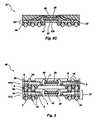
- FIG. 1Ais top view of an interposer incorporating teachings of the present invention
- FIG. 1Bis a top view of an interposer area depicted in FIG. 1A ;
- FIG. 1Cis a cross-sectional representation of the interposer area depicted in FIG. 1B ;
- FIG. 2Ais a cross-sectional representation of a semiconductor device package incorporating the teachings of the present invention.
- FIG. 2Bis a cross-sectional representation of a variation of the semiconductor device package illustrated in FIG. 2A ;
- FIG. 2Cis a cross-sectional representation of the semiconductor device package illustrated in FIG. 2A with an increased thermal element area for heat dissipation;
- FIG. 2Dis a cross section of the semiconductor package illustrated in FIG. 2A with both an increased thermal element area and thermally conductive structures attached thereto;
- FIG. 2Eis a cross-sectional representation of the semiconductor device package illustrated in FIG. 2A with an increased area for thermally conductive structures and at least one heat transfer element attached thereto;
- FIG. 3is a cross-sectional representation of an exemplary embodiment of a multi-chip module incorporating teachings of the present invention, in which a series of separately packaged semiconductor devices are positioned in a stacked arrangement;
- FIG. 4Ais a cross-sectional representation of another exemplary embodiment of a multi-chip module incorporating teachings of the present invention, wherein semiconductor devices are stacked over and electrically connected to a single interposer;
- FIGS. 4B , 4 C, and 4 Dare cross-sectional representations of variations of the multi-chip module in FIG. 4A ;
- FIG. 5is a cross-sectional representation of another exemplary embodiment of an interposer of the present invention, which includes a recess for at least partially receiving a semiconductor device, as well as a semiconductor device assembly including the interposer;
- FIG. 6is a cross-sectional representation of yet another exemplary embodiment of an interposer according to the present invention, which is configured to have at least one semiconductor device flip-chip bonded thereto, as well as an assembly including the interposer and a semiconductor device;
- FIG. 7is a cross-sectional representation of an interposer that incorporates teachings of the present invention and includes a semiconductor device flip-chip bonded to the same side thereof as that from which conductive structures protrude, as well as a semiconductor device assembly including the interposer; and
- FIG. 8is a side view of a multi-chip module including a plurality of semiconductor devices positioned at different lateral locations on the same interposer.
- the present inventionincludes an interposer for use in semiconductor device assemblies and packages, assemblies and packages including the interposer, and multi-chip modules.
- the present inventionalso includes methods for designing and forming the interposer, as well as for forming semiconductor device assemblies and packages that include the interposer.
- the interposer 20includes a substrate 12 , which is also referred to herein as an “interposer substrate,” and at least one layer 52 of conductive structures.
- the at least one layer 52 of conductive structuresincludes first contact pads 4 located proximate an attach location or region 7 on the substrate 12 and conductive traces 8 extending somewhat laterally from corresponding first contact pads 4 to corresponding second contact pads 2 .
- apertures 14 that are formed at least partially through the substrate 12expose second contact pads 2 therethrough.
- the substrate 12may be formed from either a rigid or flexible material and may comprise a substantially planar member. Silicon or another semiconductor material (e.g., gallium arsenide, indium phosphide, etc.) may be used to form the substrate 12 with at least some surfaces thereof, including those that will contact or be located proximate to the conductive structures of the interposer 20 or another semiconductor device component to be assembled therewith, being covered with an electrically insulative material (e.g., a silicon oxide or silicon nitride) to prevent electrical shorting of the conductive structures of the interposer 20 .
- electrically insulative materiale.g., a silicon oxide or silicon nitride
- suitable materials for forming the interposer substrate 12include, without limitation, FR-4 resin, glass, ceramics, and polyimide.
- the second contact pads 2 of the interposer 20are arranged to provide a desired pattern, or “footprint”, of electrical connections to facilitate communication between at least one semiconductor device to be secured to the interposer 20 and external electronic devices through a larger-scale substrate, such as a circuit board or other carrier.
- FIGS. 1B and 1Cdepict a second contact pad 2 of an interposer 20 incorporating teachings of the present invention.
- Conductive materialsuch as copper, aluminum, gold, or other conductive material, that is carried by the substrate 12 forms the second contact pads 2 , as well as the conductive traces 8 and the first contact pads 4 .
- the second contact pads 2are part of a layer 52 of conductive structures that is carried upon a surface of the substrate 12 , areas of the substrate 12 that are superimposed by the second contact pads 2 are substantially removed to form receptacles 11 , which facilitate the formation of electrical connections between the second contact pads 2 of the interposer 20 and other components, such as a circuit board or other carrier.
- the receptacles 11are configured to at least partially receive conductive structures, such as balls, bumps, columns, pins, or other elements formed from conductive material such as a metal or metal alloy (e.g., solder) or a conductive or conductor-filled elastomer.
- conductive structuressuch as balls, bumps, columns, pins, or other elements formed from conductive material such as a metal or metal alloy (e.g., solder) or a conductive or conductor-filled elastomer.
- conductive materialsuch as a metal or metal alloy (e.g., solder) or a conductive or conductor-filled elastomer.
- the second contact pads 2have a larger surface area than the adjacent end of the receptacle 11 corresponding thereto so that the substrate 12 will still provide adequate peripheral support for each second contact pad 2 .
- a protective layer 80may be formed or positioned over conductive traces 8 and second contact pads 2 , opposite from substrate 12 .
- Protective layer 80may provide additional physical support for second contact pads 2 , as well as for conductive traces 8 .
- protective layer 80electrically insulates conductive traces 8 and second contact pads 2 .
- Exemplary materials that may be used to form protective layer 80include, but are not limited to, dielectric polymers, such as polyimide.
- a dielectric polymermay be coated over conductive traces 8 and second contact pads 2 by known processes (e.g., spin-on coating, use of a doctor blade, screen printing, sprayed on, etc.) or may comprise a preformed film (e.g., polyimide tape) that is adhered to substrate 12 over conductive traces 8 and second contact pads 2 .
- a preformed filme.g., polyimide tape
- receptacles 11 in the interposer 20 of the present inventionmay shorten the physical lengths of circuits between the first contact pads 4 and their corresponding second contact pads 2 , which may reduce electrical inductance relative to that of a more conventional interposer by eliminating the need for conductive vias extending through the thickness of the substrate 12 .
- FIG. 1Cdepicts a receptacle 11 as exposing a second contact pad 2
- the receptacles 11may alternatively expose a portion of a conductive trace 8 , a first contact pad 4 , or another feature along a conductive path between a first contact pad 4 and its corresponding second contact pad 2 .
- some receptacles 11may facilitate testing of particular circuits once conductive structures have been secured to the second contact pads 2 of the interposer 20 and one or more semiconductor devices have been assembled therewith.
- the receptacles 11may be formed with draft angles, countersinks, chamfers, or radii or, alternatively, as recesses with substantially vertical sides.
- the cross-sectional shapes of the receptacles 11taken transverse to the depths thereof, may have circular, rectangular, or other desired shapes.
- Any process that is suitable for removing material of the type from which the interposer substrate 12 is formedmay be used to form the receptacles 11 .
- mask and etch processesmay be used to form receptacles 11 in a substrate 12 that is formed from a semiconductor material, glass, or ceramic.
- Substrates 12 that are formed from resins, or polymers,may have receptacles 11 formed therein by mechanical processes, such as drilling (including laser drilling), punching, milling, or die cutting.
- the interposer 20 of the present inventionmay include a thermally conductive element 6 , which may be formed from a thermally conductive material (i.e., a material conducive to heat transfer), such as copper, aluminum, gold, or the like.
- the thermally conductive element 6may increase the overall thermal mass of the interposer 20 and, thus, act as a so-called “heat sink” for a semiconductor device positioned in thermal communication therewith.
- the thermally conductive element 6is located completely within the attach region 7 .
- a thermally conductive element 6may be located only partially within the attach region 7 or lie completely outside of the attach region 7 and proximate thereto.
- the thermally conductive element 6is configured to thermally communicate with a semiconductor device disposed upon the interposer 20 so as to convey heat therefrom during operation of the semiconductor device.
- the thermally conductive element 6may comprise a part of the at least one layer 52 of conductive structures and may be formed from the same material as one or more of the other conductive structures of that layer 52 .
- the thermally conductive element 6is electrically isolated from other electrically conductive structures of the interposer 20 .
- the interposer 20may also include a ground plane 5 .
- the thermally conductive element 6 and the ground plane 5may comprise the same element or separate elements from one another.
- the ground plane 5may be positioned completely within, partially within, or proximate to an attach region 7 of the interposer substrate 12 .
- Some of the receptacles 11 that are formed at least partially through the interposer substrate 12may expose portions of a ground plane 5 , a thermally conductive element 6 , or a contact pad that communicates with the ground plane 5 and/or thermally conductive element 6 .
- the location, volume, and shape of each such receptacle 11may be tailored to provide particular heat dissipation characteristics.
- grooves (not shown) or other structuresmay be formed partially or completely through the interposer substrate 12 to expose portions of a thermally conductive element 6 and to facilitate the transfer of heat away from an assembly or package including the interposer 20 .
- structuressuch as receptacles 11 and/or grooves (not shown) that facilitate the transfer of heat away from the thermally conductive element 6 may be distributed across the substrate 12 over roughly the same area as that occupied by thermally conductive element 6 .
- an aperture 14 ′may be formed through the interposer substrate 12 ′ to expose a large, central portion of the thermally conductive element 6 therethrough, with at least some peripheral regions of the thermally conductive element 6 being secured to and supported by the interposer substrate 12 ′.
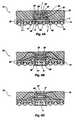
- a package 21 including the above-described interposer 20 and a semiconductor device 36 (e.g., the illustrated semiconductor die) affixed theretois depicted.
- the semiconductor device 36may be secured to an attach region 7 of the interposer 20 by way of a die attach material 38 , such as a suitable adhesive or adhesive-coated element.
- Bond pads 42 of the semiconductor device 36may be electrically connected with corresponding first contact pads 4 of the interposer 20 by way of bond wires 32 or other intermediate conductive elements (e.g., leads, TAB elements carried by a dielectric film, etc.) that are secured to second contact pads 2 formed on the top surface 10 ( FIG. 1A ) thereof.
- package 21includes electrically conductive structures 34 secured to at least some of the second contact pads 2 of the substrate 12 ′.
- the electrically conductive structures 34are positioned at least partially within the receptacles 11 formed in the interposer substrate 12 ′ and, thus, are at least partially laterally surrounded by the interposer substrate 12 ′.
- Electrically conductive structures 34may also be secured to a ground plane 5 of the interposer 20 or a contact (not shown in FIG. 2A ) that communicates with the ground plane 5 .
- Thermally conductive structures 50which resemble and may be formed from the same materials as those from which the electrically conductive structures 34 are formed, may be secured to a thermally conductive element 6 of the interposer 20 or to a contact (not shown in FIG. 2A ) that communicates with the thermally conductive element 6 .
- the thermally conductive structures 50may increase the overall thermal mass of a package 21 and, thus, act as a heat sink for the adjacent thermally conductive element 6 , as well as for a semiconductor device 36 in communication with the thermally conductive element 6 .
- the conductive structures 34 / 50 protruding therefrommay be formed from a material that is both electrically and thermally conductive.
- the electrically conductive structures 34may, by way of example only, comprise balls, bumps, columns, pins, or other structures that are formed from an electrically conductive material, such as a metal, a metal alloy (e.g., solder), a conductive elastomer, or a conductor-filled elastomer.
- the thermally conductive structures 50may be formed from a metal, a metal alloy, or another thermally conductive material.
- the electrically conductive structures 34 or thermally conductive structures 50comprise solder, another metal alloy, or a metal
- these structuresmay be formed, as known in the art, by use of a solder mask 40 that has been secured to (in the case of a preformed film solder mask) or formed on (in the case of an applied solder mask material) the substrate 12 ′ of interposer 20 .
- the solder mask 40may remain in place adjacent to the interposer 20 or, optionally, be removed from the interposer 20 .
- each semiconductor device 36may be partially or fully covered with an encapsulant material 30 of a known type, such as a suitable pot mold material, transfer mold material, glob top material, conformal coating material, or the like.
- an encapsulant material 30protects the covered regions of each semiconductor device 36 , as well as the bond wires 32 or other intermediate conductive elements that electrically connect the bond pads 42 of the semiconductor device 36 and their corresponding first contact pads 4 on the interposer 20 .
- a package 21 of the present inventionmay have a total thickness of less than about 0.8 mm, making it suitable for use in compact electronic devices, such as cellular telephones, handheld computers, and portable computers, where such low-profile packages are required or desired.
- FIG. 2Bdepicts a variation of package 21 , in which the ends of the thermally conductive structures 50 that protrude from the interposer 20 are connected to one another by way of a heat transfer element 48 .
- the heat transfer element 48which further increases the overall thermal mass of the package 21 and, therefore, provides heat sink properties, effectively increases the surface area from which heat may dissipate and may, thereby, increase the rate at which the package 21 is able to dissipate heat by way of convection or radiation.
- the heat transfer element 48is a substantially planar, unitary structure. Alternatively, the heat transfer element 48 may be formed from a number of separate sections.
- the heat transfer element 48may optionally include holes, cut-outs, varying cross-sectional properties, or the like, or some combination thereof.
- a surface 51 of the heat transfer element 48may be mechanically, chemically, or otherwise configured to further enhance the ability of the heat transfer element 48 to dissipate heat from the semiconductor device 36 .
- chemical treatments of the surface 51 of heat transfer element 48processes such as coating, greening, or blackening may be employed to increase the emissivity of the heat transfer element 48 for radioactive heat transfer.
- mechanical configuration of the surface 51 of the heat transfer element 48 to enhance its heat dissipative propertiesinclude geometrical enhancements such as grooves, roughening, or other processes that increase the area of the surface 51 .
- Such surface treatmentsmay be effected before or after the heat transfer element 48 is attached to the thermally conductive structures 50 .
- One or more regions of the surface of the heat transfer element 48may also be coated with dielectric material to prevent electrical shorting.
- FIGS. 2C-2Edepict another embodiment of a package 21 ′, which includes an interposer 20 ′ with an interposer substrate 12 ′ that includes an aperture 14 ′ formed therethrough to expose a large portion of the central region of a thermally conductive element 6 that underlies a back side 37 of a semiconductor device 36 . At least some of the peripheral edges of the thermally conductive element 6 overlap a surface of the interposer substrate 12 ′ and are physically supported thereby. Also, the solder mask 40 of package 21 ′, if any, does not extend over this portion of the thermally conductive element 6 .
- the exposed portion of the thermally conductive element 6may remain exposed through the interposer substrate 12 ′, as depicted in FIG. 2C . Any exposed regions of the surface of the thermally conductive element 6 may be chemically or mechanically treated in such a way as to enhance the thermally dissipative properties thereof, as well as to form an electrically insulative coating thereon.
- the package 21 ′may include thermally conductive structures 50 that are positioned within the aperture 14 ′, secured to and protrude from exposed regions of the thermally conductive element 6 , and are at least partially laterally surrounded by the interposer substrate 12 ′.
- FIG. 2Edepicts another alternative, in which the package 21 ′ includes a heat transfer element 48 secured to thermally conductive structures 50 that are secured to and protrude from the thermally conductive element 6 .
- Interposer 20 ′′includes a receptacle 22 that is configured to at least partially receive a semiconductor device 36 to be electrically connected thereto.
- the remaining features of interposer 20 ′′are substantially the same as those of interposer 20 shown in FIGS. 1A-1C .
- FIG. 6depicts another embodiment of an interposer 120 , of which the first contact pads 4 are positioned in an attach region 7 and positioned to mirror the locations of bond pads 42 so as to facilitate flip-chip attachment of a semiconductor device 36 thereto.
- the remaining features of interposer 120are substantially the same as those of interposer 20 shown in FIGS. 1A-1C .
- Interposer 120 ′′includes a receptacle 22 ′′ formed in the same surface as that to which receptacles 11 open.
- Receptacle 22 ′′is configured to at least partially receive a semiconductor device 36 in a flip-chip orientation. Accordingly, first contact pads 4 ′′ are positioned within the receptacle 22 ′′.
- Conductive traces 8 ′′ that communicate with the first contact pads 4 ′′extend across the interposer substrate 12 ′′, either on a surface thereof, as shown, or internally therethrough.
- the conductive traces 8 ′′extend laterally to the locations of corresponding second contact pads 2 ′′, which are exposed through the receptacles 11 that are formed through the interposer substrate 12 ′′ so as to at least partially expose corresponding second contact pads 2 ′′.
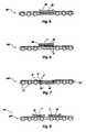
- the multi-chip module 60includes two packages 121 : an upper package 121 U and a lower package 121 L.
- At least the lower package 121 L of such a multi-chip module 60includes an aperture 9 formed through the top of the encapsulant material 30 thereof.
- Each aperture 9is configured to at least partially receive a corresponding conductive structure 34 that protrudes from the bottom of an overlying upper package 121 U.
- a contact pad of a third set, which contact pad is referred to herein as a third contact pad 16is exposed within each aperture 9 .
- Some third contact pads 16 of the package 121may communicate with corresponding first contact pads 4 and, thus, ultimately, with the bond pads 42 and corresponding internal circuitry a semiconductor device 36 of the package 121 by way of a conductive trace 8 positioned between the third contact pad 16 and the corresponding first contact pad 4 .
- Some third contact pads 16 of the package 121may communicate with corresponding second contact pads 2 and, thus, ultimately with one or more electronic components that are external to the package 121 by way of a via 15 or other conductive element positioned between the third contact pad 16 and the corresponding second contact pad 2 .
- a conductive structure 34 that protrudes from an upper package 121 U and its corresponding third contact pad 16 of the next-lower package 121 Lmay facilitate communication between a semiconductor device 36 of the upper package 121 U and either a semiconductor device 36 of the next-lower package 121 L or an external electronic device.
- the overall thickness of the multi-chip module 60 depicted in FIG. 3may be about 1.5 mm since the apertures 9 at least partially receive the heights of the electrically conductive structures 34 that protrude from the upper package 121 U.
- FIG. 3depicts a multi-chip module 60 that includes two vertically stacked packages 121 U and 121 L, it will be understood that a multi-chip module incorporating teachings of the present invention may include more than two packages.
- Another exemplary embodiment of multi-chip module incorporating teachings of the present inventionmay be formed by securing multiple semiconductor devices to a single interposer.
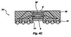
- the semiconductor devicesmay be positioned at different locations on the interposer, as shown in FIG. 8 , or stacked over one or more locations of the interposer, as shown in FIGS. 4A-4D .
- a multi-chip module 70that includes a single interposer 20 with semiconductor devices 36 , 36 ′ stacked over the same attach region 7 thereof is depicted.
- the lower semiconductor device 36is secured to the interposer 20 by way of a die attach material 38 , while another quantity of die attach material 39 , such as a suitable adhesive or adhesive-coated element, secures the upper semiconductor device 36 ′ to the lower semiconductor device 36 .
- Intermediate conductive elementssuch as the depicted bond wires 32 , 32 ′, electrically connect respective bond pads 42 , 42 ′ of the semiconductor devices 36 , 36 ′ to corresponding first contact pads 4 , 4 ′ of the interposer 20 .
- the multi-chip module 70may also include electrically conductive structures 34 and/or thermally conductive structures 50 that communicate with second contact pads 2 ( FIGS. 1A-1C ) and a thermally conductive element 6 , respectively.
- Such a multi-chip module 70 assemblymay be packaged, as known in the art, such as by applying a suitable encapsulant material 30 (e.g., a glob-top type encapsulant, a transfer molded or pot molded type encapsulant, etc.) over at least portions of semiconductor devices 36 , 36 ′, the intermediate conductive elements (e.g., bond wires 32 , 32 ′), and at least portions of the interposer 20 .
- a suitable encapsulant material 30e.g., a glob-top type encapsulant, a transfer molded or pot molded type encapsulant, etc.
- FIG. 4Ba multi-chip module 70 ′ that includes a plurality of semiconductor devices 36 , 36 ′ and an interposer 20 ′ of the type depicted in FIGS. 2A-2C is illustrated.
- the thermally conductive structures 50 of the multi-chip module 70 ′are positioned within the aperture 14 ′ formed through the substrate 12 ′ of the interposer 20 ′ and are secured directly to the thermally conductive element 6 .
- the multi-chip module 70 ′may include a heat transfer element 48 secured to at least some of the thermally conductive structures 50 .
- FIG. 4Cillustrates an embodiment of multi-chip module 70 ′ in which the thermally conductive element 6 is exposed through the aperture 14 ′ formed through the interposer substrate 12 ′.
- a second thermally conductive element 6 ′may be positioned over an active surface 35 ′ of the upper semiconductor device 36 ′ to facilitate the dissipation of heat therefrom.
- at least a portion of the second thermally conductive element 6 ′may be exposed through an encapsulant material 30 that covers portions of the upper semiconductor device 36 ′.
- one or more surfaces of the second thermally conductive element 6 ′may be chemically or mechanically treated so as to improve the heat dissipation characteristics thereof.
- an interposer 20 ′′′ with more than one attach region 7 thereonmay be used to form a multi-chip module 70 ′′′ with semiconductor devices 36 at different lateral positions.
- each semiconductor device 36may be secured and electrically connected to such an interposer 20 ′′′ as described above with reference to FIG. 2A .
Landscapes
- Engineering & Computer Science (AREA)
- Power Engineering (AREA)
- Microelectronics & Electronic Packaging (AREA)
- Physics & Mathematics (AREA)
- Condensed Matter Physics & Semiconductors (AREA)
- General Physics & Mathematics (AREA)
- Computer Hardware Design (AREA)
- Chemical & Material Sciences (AREA)
- Materials Engineering (AREA)
- Cooling Or The Like Of Semiconductors Or Solid State Devices (AREA)
- Wire Bonding (AREA)
- Structures For Mounting Electric Components On Printed Circuit Boards (AREA)
Abstract
Description
Claims (46)
Priority Applications (2)
| Application Number | Priority Date | Filing Date | Title |
|---|---|---|---|
| US11/398,912US7902648B2 (en) | 2002-03-04 | 2006-04-06 | Interposer configured to reduce the profiles of semiconductor device assemblies, packages including the same, and methods |
| US13/043,037US8269326B2 (en) | 2002-03-04 | 2011-03-08 | Semiconductor device assemblies |
Applications Claiming Priority (4)
| Application Number | Priority Date | Filing Date | Title |
|---|---|---|---|
| SG200201263ASG111935A1 (en) | 2002-03-04 | 2002-03-04 | Interposer configured to reduce the profiles of semiconductor device assemblies and packages including the same and methods |
| SG200201263-1 | 2002-03-04 | ||
| US10/150,893US7145225B2 (en) | 2002-03-04 | 2002-05-17 | Interposer configured to reduce the profiles of semiconductor device assemblies and packages including the same and methods |
| US11/398,912US7902648B2 (en) | 2002-03-04 | 2006-04-06 | Interposer configured to reduce the profiles of semiconductor device assemblies, packages including the same, and methods |
Related Parent Applications (1)
| Application Number | Title | Priority Date | Filing Date |
|---|---|---|---|
| US10/150,893ContinuationUS7145225B2 (en) | 2002-03-04 | 2002-05-17 | Interposer configured to reduce the profiles of semiconductor device assemblies and packages including the same and methods |
Related Child Applications (1)
| Application Number | Title | Priority Date | Filing Date |
|---|---|---|---|
| US13/043,037ContinuationUS8269326B2 (en) | 2002-03-04 | 2011-03-08 | Semiconductor device assemblies |
Publications (2)
| Publication Number | Publication Date |
|---|---|
| US20060175690A1 US20060175690A1 (en) | 2006-08-10 |
| US7902648B2true US7902648B2 (en) | 2011-03-08 |
Family
ID=27800897
Family Applications (3)
| Application Number | Title | Priority Date | Filing Date |
|---|---|---|---|
| US10/150,893Expired - LifetimeUS7145225B2 (en) | 2002-03-04 | 2002-05-17 | Interposer configured to reduce the profiles of semiconductor device assemblies and packages including the same and methods |
| US11/398,912Expired - LifetimeUS7902648B2 (en) | 2002-03-04 | 2006-04-06 | Interposer configured to reduce the profiles of semiconductor device assemblies, packages including the same, and methods |
| US13/043,037Expired - Fee RelatedUS8269326B2 (en) | 2002-03-04 | 2011-03-08 | Semiconductor device assemblies |
Family Applications Before (1)
| Application Number | Title | Priority Date | Filing Date |
|---|---|---|---|
| US10/150,893Expired - LifetimeUS7145225B2 (en) | 2002-03-04 | 2002-05-17 | Interposer configured to reduce the profiles of semiconductor device assemblies and packages including the same and methods |
Family Applications After (1)
| Application Number | Title | Priority Date | Filing Date |
|---|---|---|---|
| US13/043,037Expired - Fee RelatedUS8269326B2 (en) | 2002-03-04 | 2011-03-08 | Semiconductor device assemblies |
Country Status (2)
| Country | Link |
|---|---|
| US (3) | US7145225B2 (en) |
| SG (1) | SG111935A1 (en) |
Cited By (12)
| Publication number | Priority date | Publication date | Assignee | Title |
|---|---|---|---|---|
| US20100288541A1 (en)* | 2009-05-13 | 2010-11-18 | Advanced Semiconductor Engineering, Inc. | Substrate having single patterned metal layer, and package applied with the substrate , and methods of manufacturing of the substrate and package |
| US20100289132A1 (en)* | 2009-05-13 | 2010-11-18 | Shih-Fu Huang | Substrate having embedded single patterned metal layer, and package applied with the same, and methods of manufacturing of the substrate and package |
| US20100314744A1 (en)* | 2009-05-13 | 2010-12-16 | Shih-Fu Huang | Substrate having single patterned metal layer exposing patterned dielectric layer, chip package structure including the substrate, and manufacturing methods thereof |
| US20110057301A1 (en)* | 2009-09-08 | 2011-03-10 | Advanced Semiconductor Engineering, Inc. | Semiconductor package |
| US20110084370A1 (en)* | 2009-10-14 | 2011-04-14 | Advanced Semiconductor Engineering, Inc. | Semiconductor package and process for fabricating same |
| US20110147925A1 (en)* | 2009-12-18 | 2011-06-23 | Nxp B.V. | Pre-soldered leadless package |
| US20110169150A1 (en)* | 2010-01-13 | 2011-07-14 | Advanced Semiconductor Engineering, Inc. | Semiconductor Package with Single Sided Substrate Design and Manufacturing Methods Thereof |
| US20110204499A1 (en)* | 2002-03-04 | 2011-08-25 | Micron Technology, Inc. | Semiconductor device assemblies |
| US20110221048A1 (en)* | 2010-03-10 | 2011-09-15 | Ken Beng Lim | Package Having Spaced Apart Heat Sink |
| US20120018860A1 (en)* | 2009-03-30 | 2012-01-26 | Toppan Printing Co., Ltd. | Method for manufacturing substrate for semiconductor element, and semiconductor device |
| US9349611B2 (en) | 2010-03-22 | 2016-05-24 | Advanced Semiconductor Engineering, Inc. | Stackable semiconductor package and manufacturing method thereof |
| US20170256513A1 (en)* | 2013-09-09 | 2017-09-07 | Taiwan Semiconductor Manufacturing Co., Ltd. | Semiconductor device having a boundary structure, a package on package structure, and a method of making |
Families Citing this family (70)
| Publication number | Priority date | Publication date | Assignee | Title |
|---|---|---|---|---|
| US6400574B1 (en)* | 2000-05-11 | 2002-06-04 | Micron Technology, Inc. | Molded ball grid array |
| SG122743A1 (en) | 2001-08-21 | 2006-06-29 | Micron Technology Inc | Microelectronic devices and methods of manufacture |
| SG121707A1 (en) | 2002-03-04 | 2006-05-26 | Micron Technology Inc | Method and apparatus for flip-chip packaging providing testing capability |
| AU2003298595A1 (en) | 2002-10-08 | 2004-05-04 | Chippac, Inc. | Semiconductor stacked multi-package module having inverted second package |
| US7034387B2 (en) | 2003-04-04 | 2006-04-25 | Chippac, Inc. | Semiconductor multipackage module including processor and memory package assemblies |
| TWI241000B (en)* | 2003-01-21 | 2005-10-01 | Siliconware Precision Industries Co Ltd | Semiconductor package and fabricating method thereof |
| KR20050016087A (en)* | 2003-08-06 | 2005-02-21 | 로무 가부시키가이샤 | Semiconductor device |
| US6946726B1 (en)* | 2003-11-26 | 2005-09-20 | Actel Corporation | Chip carrier substrate with a land grid array and external bond terminals |
| US7345361B2 (en)* | 2003-12-04 | 2008-03-18 | Intel Corporation | Stackable integrated circuit packaging |
| DE112004002527T5 (en)* | 2004-01-06 | 2008-03-06 | Infineon Technologies Ag | Method for encapsulating circuit chips |
| TWI233170B (en)* | 2004-02-05 | 2005-05-21 | United Microelectronics Corp | Ultra-thin wafer level stack packaging method and structure using thereof |
| KR101014576B1 (en)* | 2004-02-24 | 2011-02-16 | 이비덴 가부시키가이샤 | Semiconductor mounting board |
| US7332921B2 (en)* | 2004-03-26 | 2008-02-19 | Cypress Semiconductor Corporation | Probe card and method for constructing same |
| SG111181A1 (en)* | 2004-04-08 | 2005-05-30 | Micron Technology Inc | Semiconductor packages, and methods of forming semiconductor packages |
| US8125076B2 (en)* | 2004-11-12 | 2012-02-28 | Stats Chippac Ltd. | Semiconductor package system with substrate heat sink |
| KR100765604B1 (en)* | 2004-11-26 | 2007-10-09 | 산요덴키가부시키가이샤 | Circuit device and manufacturing method thereof |
| US20060270104A1 (en)* | 2005-05-03 | 2006-11-30 | Octavio Trovarelli | Method for attaching dice to a package and arrangement of dice in a package |
| US8327104B2 (en) | 2006-07-31 | 2012-12-04 | Google Inc. | Adjusting the timing of signals associated with a memory system |
| US8438328B2 (en)* | 2008-02-21 | 2013-05-07 | Google Inc. | Emulation of abstracted DIMMs using abstracted DRAMs |
| US10013371B2 (en) | 2005-06-24 | 2018-07-03 | Google Llc | Configurable memory circuit system and method |
| US9507739B2 (en) | 2005-06-24 | 2016-11-29 | Google Inc. | Configurable memory circuit system and method |
| US8060774B2 (en) | 2005-06-24 | 2011-11-15 | Google Inc. | Memory systems and memory modules |
| US8359187B2 (en) | 2005-06-24 | 2013-01-22 | Google Inc. | Simulating a different number of memory circuit devices |
| US9171585B2 (en) | 2005-06-24 | 2015-10-27 | Google Inc. | Configurable memory circuit system and method |
| US8111566B1 (en) | 2007-11-16 | 2012-02-07 | Google, Inc. | Optimal channel design for memory devices for providing a high-speed memory interface |
| US8397013B1 (en) | 2006-10-05 | 2013-03-12 | Google Inc. | Hybrid memory module |
| US8130560B1 (en) | 2006-11-13 | 2012-03-06 | Google Inc. | Multi-rank partial width memory modules |
| US9542352B2 (en) | 2006-02-09 | 2017-01-10 | Google Inc. | System and method for reducing command scheduling constraints of memory circuits |
| US8335894B1 (en) | 2008-07-25 | 2012-12-18 | Google Inc. | Configurable memory system with interface circuit |
| US8386722B1 (en) | 2008-06-23 | 2013-02-26 | Google Inc. | Stacked DIMM memory interface |
| US8796830B1 (en) | 2006-09-01 | 2014-08-05 | Google Inc. | Stackable low-profile lead frame package |
| US8090897B2 (en) | 2006-07-31 | 2012-01-03 | Google Inc. | System and method for simulating an aspect of a memory circuit |
| US7386656B2 (en) | 2006-07-31 | 2008-06-10 | Metaram, Inc. | Interface circuit system and method for performing power management operations in conjunction with only a portion of a memory circuit |
| US20080082763A1 (en) | 2006-10-02 | 2008-04-03 | Metaram, Inc. | Apparatus and method for power management of memory circuits by a system or component thereof |
| US8077535B2 (en) | 2006-07-31 | 2011-12-13 | Google Inc. | Memory refresh apparatus and method |
| US8055833B2 (en) | 2006-10-05 | 2011-11-08 | Google Inc. | System and method for increasing capacity, performance, and flexibility of flash storage |
| US7609567B2 (en) | 2005-06-24 | 2009-10-27 | Metaram, Inc. | System and method for simulating an aspect of a memory circuit |
| US8081474B1 (en) | 2007-12-18 | 2011-12-20 | Google Inc. | Embossed heat spreader |
| US8244971B2 (en) | 2006-07-31 | 2012-08-14 | Google Inc. | Memory circuit system and method |
| US8041881B2 (en) | 2006-07-31 | 2011-10-18 | Google Inc. | Memory device with emulated characteristics |
| US8089795B2 (en) | 2006-02-09 | 2012-01-03 | Google Inc. | Memory module with memory stack and interface with enhanced capabilities |
| US20080028136A1 (en) | 2006-07-31 | 2008-01-31 | Schakel Keith R | Method and apparatus for refresh management of memory modules |
| US7245013B2 (en)* | 2005-07-26 | 2007-07-17 | Infineon Technologies Ag | Substrate based IC-package |
| WO2007028109A2 (en) | 2005-09-02 | 2007-03-08 | Metaram, Inc. | Methods and apparatus of stacking drams |
| US9632929B2 (en) | 2006-02-09 | 2017-04-25 | Google Inc. | Translating an address associated with a command communicated between a system and memory circuits |
| US8502362B2 (en)* | 2011-08-16 | 2013-08-06 | Advanced Analogic Technologies, Incorporated | Semiconductor package containing silicon-on-insulator die mounted in bump-on-leadframe manner to provide low thermal resistance |
| US7724589B2 (en) | 2006-07-31 | 2010-05-25 | Google Inc. | System and method for delaying a signal communicated from a system to at least one of a plurality of memory circuits |
| US7888185B2 (en)* | 2006-08-17 | 2011-02-15 | Micron Technology, Inc. | Semiconductor device assemblies and systems including at least one conductive pathway extending around a side of at least one semiconductor device |
| DE112006004099B4 (en)* | 2006-11-14 | 2013-08-22 | Infineon Technologies Ag | Electronic component and method for its production |
| JP4897451B2 (en)* | 2006-12-04 | 2012-03-14 | ルネサスエレクトロニクス株式会社 | Semiconductor device |
| KR101323978B1 (en)* | 2006-12-21 | 2013-10-30 | 에이저 시스템즈 엘엘시 | High thermal performance packaging for circuit dies |
| US7926173B2 (en)* | 2007-07-05 | 2011-04-19 | Occam Portfolio Llc | Method of making a circuit assembly |
| TW200906260A (en)* | 2007-07-20 | 2009-02-01 | Siliconware Precision Industries Co Ltd | Circuit board structure and fabrication method thereof |
| US8080874B1 (en) | 2007-09-14 | 2011-12-20 | Google Inc. | Providing additional space between an integrated circuit and a circuit board for positioning a component therebetween |
| US20090279275A1 (en)* | 2008-05-09 | 2009-11-12 | Stephen Peter Ayotte | Method of attaching an integrated circuit chip to a module |
| DE202010017690U1 (en) | 2009-06-09 | 2012-05-29 | Google, Inc. | Programming dimming terminating resistor values |
| US8426961B2 (en)* | 2010-06-25 | 2013-04-23 | Taiwan Semiconductor Manufacturing Company, Ltd. | Embedded 3D interposer structure |
| US9337116B2 (en)* | 2010-10-28 | 2016-05-10 | Stats Chippac, Ltd. | Semiconductor device and method of forming stepped interposer for stacking and electrically connecting semiconductor die |
| US20130234317A1 (en) | 2012-03-09 | 2013-09-12 | Taiwan Semiconductor Manufacturing Company, Ltd. | Packaging Methods and Packaged Semiconductor Devices |
| US9263412B2 (en) | 2012-03-09 | 2016-02-16 | Taiwan Semiconductor Manufacturing Company, Ltd. | Packaging methods and packaged semiconductor devices |
| US8853849B2 (en)* | 2013-03-06 | 2014-10-07 | Infineon Technologies Austria Ag | Package arrangement and a method of manufacturing a package arrangement |
| US10475732B2 (en) | 2013-07-12 | 2019-11-12 | Taiwan Semiconductor Manufacturing Co., Ltd. | 3DIC package integration for high-frequency RF system |
| CN103456645B (en)* | 2013-08-06 | 2016-06-01 | 江阴芯智联电子科技有限公司 | First lose and seal three-dimensional systematic chip afterwards and just filling stack package structure and processing method |
| CN103413766B (en)* | 2013-08-06 | 2016-08-10 | 江阴芯智联电子科技有限公司 | First sealing chip formal dress three-dimensional systematic metallic circuit plate structure and process after erosion |
| CN103400771B (en)* | 2013-08-06 | 2016-06-29 | 江阴芯智联电子科技有限公司 | First sealing chip upside-down mounting three-dimensional systematic metal circuit board structure and process after erosion |
| US9425125B2 (en) | 2014-02-20 | 2016-08-23 | Altera Corporation | Silicon-glass hybrid interposer circuitry |
| CN105280597A (en)* | 2014-07-23 | 2016-01-27 | 华天科技(西安)有限公司 | Packaging member for reducing width of lead wire by using grinding technology and manufacture process thereof |
| US9679873B2 (en) | 2015-06-18 | 2017-06-13 | Qualcomm Incorporated | Low profile integrated circuit (IC) package comprising a plurality of dies |
| WO2018063196A1 (en)* | 2016-09-28 | 2018-04-05 | Intel IP Corporation | Systems, methods, and apparatuses for implementing reduced height semiconductor packages for mobile electronics |
| US12322716B2 (en)* | 2022-03-10 | 2025-06-03 | Taiwan Semiconductor Manufacturing Co., Ltd. | Heat dissipating features for laser drilling process |
Citations (208)
| Publication number | Priority date | Publication date | Assignee | Title |
|---|---|---|---|---|
| US3239496A (en) | 1962-09-24 | 1966-03-08 | Nalco Chemical Co | Method for producing polymeric salts of aminoalkylacrylates |
| US4074342A (en) | 1974-12-20 | 1978-02-14 | International Business Machines Corporation | Electrical package for lsi devices and assembly process therefor |
| US4807021A (en) | 1986-03-10 | 1989-02-21 | Kabushiki Kaisha Toshiba | Semiconductor device having stacking structure |
| US4818728A (en) | 1986-12-03 | 1989-04-04 | Sharp Kabushiki Kaisha | Method of making a hybrid semiconductor device |
| US4954875A (en) | 1986-07-17 | 1990-09-04 | Laser Dynamics, Inc. | Semiconductor wafer array with electrically conductive compliant material |
| EP0475022A1 (en) | 1990-09-13 | 1992-03-18 | International Business Machines Corporation | Direct attachment of semiconductor chips to a substrate with a thermoplastic interposer |
| US5148265A (en) | 1990-09-24 | 1992-09-15 | Ist Associates, Inc. | Semiconductor chip assemblies with fan-in leads |
| US5258648A (en) | 1991-06-27 | 1993-11-02 | Motorola, Inc. | Composite flip chip semiconductor device with an interposer having test contacts formed along its periphery |
| US5346861A (en) | 1990-09-24 | 1994-09-13 | Tessera, Inc. | Semiconductor chip assemblies and methods of making same |
| US5366794A (en) | 1991-07-30 | 1994-11-22 | Mitsubishi Denki Kabushiki Kaisha | Tape carrier for semiconductor apparatus |
| US5385869A (en) | 1993-07-22 | 1995-01-31 | Motorola, Inc. | Semiconductor chip bonded to a substrate and method of making |
| US5386341A (en) | 1993-11-01 | 1995-01-31 | Motorola, Inc. | Flexible substrate folded in a U-shape with a rigidizer plate located in the notch of the U-shape |
| US5394303A (en) | 1992-09-11 | 1995-02-28 | Kabushiki Kaisha Toshiba | Semiconductor device |
| US5397921A (en) | 1993-09-03 | 1995-03-14 | Advanced Semiconductor Assembly Technology | Tab grid array |
| US5404044A (en) | 1992-09-29 | 1995-04-04 | International Business Machines Corporation | Parallel process interposer (PPI) |
| US5422205A (en) | 1993-03-03 | 1995-06-06 | Kabushiki Kaisha Toshiba | Micropattern forming method |
| US5422615A (en)* | 1992-09-14 | 1995-06-06 | Hitachi, Ltd. | High frequency circuit device |
| US5438477A (en) | 1993-08-12 | 1995-08-01 | Lsi Logic Corporation | Die-attach technique for flip-chip style mounting of semiconductor dies |
| US5448511A (en) | 1994-06-01 | 1995-09-05 | Storage Technology Corporation | Memory stack with an integrated interconnect and mounting structure |
| US5468995A (en) | 1994-07-05 | 1995-11-21 | Motorola, Inc. | Semiconductor device having compliant columnar electrical connections |
| US5468681A (en) | 1989-08-28 | 1995-11-21 | Lsi Logic Corporation | Process for interconnecting conductive substrates using an interposer having conductive plastic filled vias |
| US5489804A (en) | 1989-08-28 | 1996-02-06 | Lsi Logic Corporation | Flexible preformed planar structures for interposing between a chip and a substrate |
| US5504277A (en) | 1993-10-26 | 1996-04-02 | Pacific Microelectronics Corporation | Solder ball array |
| US5598033A (en) | 1995-10-16 | 1997-01-28 | Advanced Micro Devices, Inc. | Micro BGA stacking scheme |
| US5608265A (en)* | 1993-03-17 | 1997-03-04 | Hitachi, Ltd. | Encapsulated semiconductor device package having holes for electrically conductive material |
| JPH0982857A (en)* | 1995-09-18 | 1997-03-28 | Nec Corp | Multi-chip package structure |
| US5646446A (en) | 1995-12-22 | 1997-07-08 | Fairchild Space And Defense Corporation | Three-dimensional flexible assembly of integrated circuits |
| US5663530A (en) | 1995-08-01 | 1997-09-02 | Minnesota Mining And Manufacturing Company | Wire bond tape ball grid array package |
| US5668405A (en) | 1994-09-14 | 1997-09-16 | Nec Corporation | Semiconductor device with a film carrier tape |
| US5674785A (en) | 1995-11-27 | 1997-10-07 | Micron Technology, Inc. | Method of producing a single piece package for semiconductor die |
| US5679977A (en) | 1990-09-24 | 1997-10-21 | Tessera, Inc. | Semiconductor chip assemblies, methods of making same and components for same |
| US5683942A (en) | 1994-05-25 | 1997-11-04 | Nec Corporation | Method for manufacturing bump leaded film carrier type semiconductor device |
| US5697148A (en) | 1995-08-22 | 1997-12-16 | Motorola, Inc. | Flip underfill injection technique |
| US5699027A (en)* | 1995-03-28 | 1997-12-16 | Matsushita Electric Industrial Co., Ltd. | Surface acoustic wave devices having a guard layer |
| US5710071A (en) | 1995-12-04 | 1998-01-20 | Motorola, Inc. | Process for underfilling a flip-chip semiconductor device |
| US5719449A (en) | 1996-09-30 | 1998-02-17 | Lucent Technologies Inc. | Flip-chip integrated circuit with improved testability |
| US5721151A (en) | 1995-06-07 | 1998-02-24 | Lsi Logic Corporation | Method of fabricating a gate array integrated circuit including interconnectable macro-arrays |
| US5723347A (en) | 1993-09-30 | 1998-03-03 | International Business Machines Corp. | Semi-conductor chip test probe and process for manufacturing the probe |
| US5742100A (en) | 1995-03-27 | 1998-04-21 | Motorola, Inc. | Structure having flip-chip connected substrates |
| US5747982A (en) | 1996-12-05 | 1998-05-05 | Lucent Technologies Inc. | Multi-chip modules with isolated coupling between modules |
| US5752182A (en) | 1994-05-09 | 1998-05-12 | Matsushita Electric Industrial Co., Ltd. | Hybrid IC |
| US5758413A (en) | 1995-09-25 | 1998-06-02 | International Business Machines Corporation | Method of manufacturing a multiple layer circuit board die carrier with fine dimension stacked vias |
| US5768109A (en) | 1991-06-26 | 1998-06-16 | Hughes Electronics | Multi-layer circuit board and semiconductor flip chip connection |
| US5777391A (en) | 1994-12-20 | 1998-07-07 | Hitachi, Ltd. | Semiconductor device having an improved connection arrangement between a semiconductor pellet and base substrate electrodes and a method of manufacture thereof |
| US5796591A (en) | 1995-06-07 | 1998-08-18 | International Business Machines Corporation | Direct chip attach circuit card |
| US5798567A (en) | 1997-08-21 | 1998-08-25 | Hewlett-Packard Company | Ball grid array integrated circuit package which employs a flip chip integrated circuit and decoupling capacitors |
| US5798285A (en) | 1995-05-25 | 1998-08-25 | International Business Machines Corpoation | Method of making electronic module with multiple solder dams in soldermask window |
| US5805422A (en) | 1994-09-21 | 1998-09-08 | Nec Corporation | Semiconductor package with flexible board and method of fabricating the same |
| US5812378A (en) | 1994-06-07 | 1998-09-22 | Tessera, Inc. | Microelectronic connector for engaging bump leads |
| US5818113A (en) | 1995-09-13 | 1998-10-06 | Kabushiki Kaisha Toshiba | Semiconductor device |
| US5834338A (en) | 1993-12-16 | 1998-11-10 | Nec Corporation | Chip carrier semiconductor device assembly and a method for forming the same |
| US5835355A (en) | 1997-09-22 | 1998-11-10 | Lsi Logic Corporation | Tape ball grid array package with perforated metal stiffener |
| US5834366A (en) | 1996-05-15 | 1998-11-10 | Micron Technology, Inc. | Method for fabricating microbump interconnect for bare semiconductor dice |
| US5834848A (en) | 1996-12-03 | 1998-11-10 | Kabushiki Kaisha Toshiba | Electronic device and semiconductor package |
| US5844315A (en) | 1996-03-26 | 1998-12-01 | Motorola Corporation | Low-profile microelectronic package |
| US5844168A (en) | 1995-08-01 | 1998-12-01 | Minnesota Mining And Manufacturing Company | Multi-layer interconnect sutructure for ball grid arrays |
| US5843808A (en) | 1996-01-11 | 1998-12-01 | Asat, Limited | Structure and method for automated assembly of a tab grid array package |
| US5866953A (en) | 1996-05-24 | 1999-02-02 | Micron Technology, Inc. | Packaged die on PCB with heat sink encapsulant |
| US5877559A (en) | 1995-06-12 | 1999-03-02 | Nitto Denko Corporation | Film carrier for fine-pitched and high density mounting and semiconductor device using same |
| US5886408A (en) | 1994-09-08 | 1999-03-23 | Fujitsu Limited | Multi-chip semiconductor device |
| US5892271A (en) | 1995-04-18 | 1999-04-06 | Nec Corporation | Semiconductor device |
| US5891753A (en) | 1997-01-24 | 1999-04-06 | Micron Technology, Inc. | Method and apparatus for packaging flip chip bare die on printed circuit boards |
| US5973389A (en) | 1997-04-22 | 1999-10-26 | International Business Machines Corporation | Semiconductor chip carrier assembly |
| US5973404A (en) | 1996-03-07 | 1999-10-26 | Micron Technology, Inc. | Underfill of bumped or raised die using a barrier adjacent to the sidewall of semiconductor device |
| US5977640A (en) | 1998-06-26 | 1999-11-02 | International Business Machines Corporation | Highly integrated chip-on-chip packaging |
| US5982030A (en) | 1998-02-27 | 1999-11-09 | Macintrye; Donald Malcom | Rigid package with low stress mounting of semiconductor die |
| US5986460A (en) | 1995-07-04 | 1999-11-16 | Ricoh Company, Ltd. | BGA package semiconductor device and inspection method therefor |
| US5984691A (en) | 1996-05-24 | 1999-11-16 | International Business Machines Corporation | Flexible circuitized interposer with apertured member and method for making same |
| US5990545A (en) | 1996-12-02 | 1999-11-23 | 3M Innovative Properties Company | Chip scale ball grid array for integrated circuit package |
| US5991161A (en) | 1997-12-19 | 1999-11-23 | Intel Corporation | Multi-chip land grid array carrier |
| US6005776A (en) | 1998-01-05 | 1999-12-21 | Intel Corporation | Vertical connector based packaging solution for integrated circuits |
| US6008543A (en) | 1995-03-09 | 1999-12-28 | Sony Corporation | Conductive bumps on pads for flip chip application |
| US6011694A (en) | 1996-08-01 | 2000-01-04 | Fuji Machinery Mfg. & Electronics Co., Ltd. | Ball grid array semiconductor package with solder ball openings in an insulative base |
| US6013948A (en) | 1995-11-27 | 2000-01-11 | Micron Technology, Inc. | Stackable chip scale semiconductor package with mating contacts on opposed surfaces |
| US6020629A (en) | 1998-06-05 | 2000-02-01 | Micron Technology, Inc. | Stacked semiconductor package and method of fabrication |
| US6022761A (en) | 1996-05-28 | 2000-02-08 | Motorola, Inc. | Method for coupling substrates and structure |
| US6024584A (en) | 1996-10-10 | 2000-02-15 | Berg Technology, Inc. | High density connector |
| US6027346A (en) | 1998-06-29 | 2000-02-22 | Xandex, Inc. | Membrane-supported contactor for semiconductor test |
| US6028365A (en) | 1998-03-30 | 2000-02-22 | Micron Technology, Inc. | Integrated circuit package and method of fabrication |
| US6034427A (en) | 1998-01-28 | 2000-03-07 | Prolinx Labs Corporation | Ball grid array structure and method for packaging an integrated circuit chip |
| US6037665A (en) | 1997-03-03 | 2000-03-14 | Nec Corporation | Mounting assembly of integrated circuit device and method for production thereof |
| US6039889A (en) | 1999-01-12 | 2000-03-21 | Fujitsu Limited | Process flows for formation of fine structure layer pairs on flexible films |
| US6040630A (en) | 1998-04-13 | 2000-03-21 | Harris Corporation | Integrated circuit package for flip chip with alignment preform feature and method of forming same |
| US6048755A (en) | 1998-11-12 | 2000-04-11 | Micron Technology, Inc. | Method for fabricating BGA package using substrate with patterned solder mask open in die attach area |
| US6050832A (en) | 1998-08-07 | 2000-04-18 | Fujitsu Limited | Chip and board stress relief interposer |
| US6057178A (en) | 1997-09-26 | 2000-05-02 | Siemens Aktiengesellschaft | Method of padding an electronic component, mounted on a flat substrate, with a liquid filler |
| EP0997942A2 (en) | 1998-10-30 | 2000-05-03 | Shinko Electric Industries Co. Ltd. | Chip Size Semiconductor Package and process for producing it |
| US6060782A (en) | 1998-01-26 | 2000-05-09 | Sharp Kabushiki Kaisha | Semiconductor device with improved mounting on tape-shaped insulating substrate |
| US6064114A (en) | 1997-12-01 | 2000-05-16 | Motorola, Inc. | Semiconductor device having a sub-chip-scale package structure and method for forming same |
| US6072233A (en) | 1998-05-04 | 2000-06-06 | Micron Technology, Inc. | Stackable ball grid array package |
| US6074897A (en) | 1996-05-01 | 2000-06-13 | Lucent Technologies Inc. | Integrated circuit bonding method and apparatus |
| US6075710A (en) | 1998-02-11 | 2000-06-13 | Express Packaging Systems, Inc. | Low-cost surface-mount compatible land-grid array (LGA) chip scale package (CSP) for packaging solder-bumped flip chips |
| EP1009027A2 (en) | 1998-12-10 | 2000-06-14 | Soshotech Co., Ltd. | Multipoint conductive sheet |
| US6093035A (en) | 1996-06-28 | 2000-07-25 | Berg Technology, Inc. | Contact for use in an electrical connector |
| US6116921A (en) | 1998-02-16 | 2000-09-12 | The Whitaker Corporation | Electrical connector having recessed solderball foot |
| US6124631A (en) | 1996-04-26 | 2000-09-26 | Centre Suisse D'electronique Et De Microtechnique Sa | Micro sensor and method for making same |
| US6127736A (en) | 1996-03-18 | 2000-10-03 | Micron Technology, Inc. | Microbump interconnect for semiconductor dice |
| US6133072A (en) | 1996-12-13 | 2000-10-17 | Tessera, Inc. | Microelectronic connector with planar elastomer sockets |
| US6133637A (en) | 1997-01-24 | 2000-10-17 | Rohm Co., Ltd. | Semiconductor device having a plurality of semiconductor chips |
| US6137183A (en) | 1997-10-24 | 2000-10-24 | Seiko Epson Corporation | Flip chip mounting method and semiconductor apparatus manufactured by the method |
| US6137062A (en) | 1998-05-11 | 2000-10-24 | Motorola, Inc. | Ball grid array with recessed solder balls |
| US6137164A (en) | 1998-03-16 | 2000-10-24 | Texas Instruments Incorporated | Thin stacked integrated circuit device |
| US6157541A (en) | 1997-12-30 | 2000-12-05 | Siemens Aktiengesellschaft | Stack arrangement for two semiconductor memory chips and printed board for accepting a plurality of such stack arrangements |
| US6165885A (en) | 1995-08-02 | 2000-12-26 | International Business Machines Corporation | Method of making components with solder balls |
| US6172422B1 (en) | 1996-07-11 | 2001-01-09 | Pfu Limited | Semiconductor device and a manufacturing method thereof |
| US6177723B1 (en) | 1997-04-10 | 2001-01-23 | Texas Instruments Incorporated | Integrated circuit package and flat plate molding process for integrated circuit package |
| US6180881B1 (en) | 1998-05-05 | 2001-01-30 | Harlan Ruben Isaak | Chip stack and method of making same |
| US6179598B1 (en) | 1997-01-28 | 2001-01-30 | Micron Technology, Inc. | Apparatus for filling a gap between spaced layers of a semiconductor |
| US6191487B1 (en) | 1998-04-23 | 2001-02-20 | Minco Technology Labs, Inc. | Semiconductor and flip chip packages and method having a back-side connection |
| US6198634B1 (en) | 1999-03-31 | 2001-03-06 | International Business Machines Corporation | Electronic package with stacked connections |
| JP2001077294A (en) | 1999-09-02 | 2001-03-23 | Nec Corp | Semiconductor device |
| US6208525B1 (en) | 1997-03-27 | 2001-03-27 | Hitachi, Ltd. | Process for mounting electronic device and semiconductor device |
| US6208521B1 (en) | 1997-05-19 | 2001-03-27 | Nitto Denko Corporation | Film carrier and laminate type mounting structure using same |
| US6212768B1 (en) | 1998-05-15 | 2001-04-10 | Nec Corporation | Flip chip mounting method and apparatus therefor |
| US6214156B1 (en) | 1996-03-19 | 2001-04-10 | Kabushiki Kaisha Toshiba | Semiconductor device mounted on board by flip-chip and method for mounting the same |
| US6218202B1 (en) | 1998-10-06 | 2001-04-17 | Texas Instruments Incorporated | Semiconductor device testing and burn-in methodology |
| US6219911B1 (en) | 1998-03-23 | 2001-04-24 | Polymer Flip Chip Corp. | Flip chip mounting technique |
| US6222265B1 (en) | 1997-03-10 | 2001-04-24 | Micron Technology, Inc. | Method of constructing stacked packages |
| US6221763B1 (en) | 1999-04-05 | 2001-04-24 | Micron Technology, Inc. | Method of forming a metal seed layer for subsequent plating |
| US6225688B1 (en) | 1997-12-11 | 2001-05-01 | Tessera, Inc. | Stacked microelectronic assembly and method therefor |
| US6229711B1 (en) | 1998-08-31 | 2001-05-08 | Shinko Electric Industries Co., Ltd. | Flip-chip mount board and flip-chip mount structure with improved mounting reliability |
| US6232666B1 (en) | 1998-12-04 | 2001-05-15 | Mciron Technology, Inc. | Interconnect for packaging semiconductor dice and fabricating BGA packages |
| US6239496B1 (en) | 1999-01-18 | 2001-05-29 | Kabushiki Kaisha Toshiba | Package having very thin semiconductor chip, multichip module assembled by the package, and method for manufacturing the same |
| US6242932B1 (en) | 1999-02-19 | 2001-06-05 | Micron Technology, Inc. | Interposer for semiconductor components having contact balls |
| KR20010058357A (en) | 1999-12-27 | 2001-07-05 | 윤종용 | Dual chip Package of socket type |
| US6262895B1 (en) | 2000-01-13 | 2001-07-17 | John A. Forthun | Stackable chip package with flex carrier |
| US6265775B1 (en) | 1997-01-24 | 2001-07-24 | Micron Technology, Inc. | Flip chip technique for chip assembly |
| US6268654B1 (en)* | 1997-04-18 | 2001-07-31 | Ankor Technology, Inc. | Integrated circuit package having adhesive bead supporting planar lid above planar substrate |
| US6271469B1 (en) | 1999-11-12 | 2001-08-07 | Intel Corporation | Direct build-up layer on an encapsulated die package |
| US6282094B1 (en)* | 1999-04-12 | 2001-08-28 | Siliconware Precision Industries, Co., Ltd. | Ball-grid array integrated circuit package with an embedded type of heat-dissipation structure and method of manufacturing the same |
| US6281046B1 (en) | 2000-04-25 | 2001-08-28 | Atmel Corporation | Method of forming an integrated circuit package at a wafer level |
| US6285081B1 (en) | 1999-07-13 | 2001-09-04 | Micron Technology, Inc. | Deflectable interconnect |
| US6291265B1 (en) | 1998-07-28 | 2001-09-18 | Micron Technology, Inc. | Method of manufacturing an interposer |
| US6291884B1 (en) | 1999-11-09 | 2001-09-18 | Amkor Technology, Inc. | Chip-size semiconductor packages |
| US6291775B1 (en) | 1998-04-21 | 2001-09-18 | Matsushita Electric Industrial Co., Ltd. | Flip chip bonding land waving prevention pattern |
| US6294455B1 (en) | 1997-08-20 | 2001-09-25 | Micron Technology, Inc. | Conductive lines, coaxial lines, integrated circuitry, and methods of forming conductive lines, coaxial lines, and integrated circuitry |
| US20010024129A1 (en) | 2000-03-23 | 2001-09-27 | Salman Akram | Interposer and methods for fabricating same |
| US6295730B1 (en) | 1999-09-02 | 2001-10-02 | Micron Technology, Inc. | Method and apparatus for forming metal contacts on a substrate |
| US6300679B1 (en) | 1998-06-01 | 2001-10-09 | Semiconductor Components Industries, Llc | Flexible substrate for packaging a semiconductor component |
| US6310288B1 (en) | 1996-05-21 | 2001-10-30 | Micron Technology, Inc. | Underfill coating for loc package |
| US6323060B1 (en) | 1999-05-05 | 2001-11-27 | Dense-Pac Microsystems, Inc. | Stackable flex circuit IC package and method of making same |
| US20010048157A1 (en) | 2000-03-16 | 2001-12-06 | Masood Murtuza | Direct attach chip scale package |
| US20010053563A1 (en) | 2000-06-20 | 2001-12-20 | Samsung Electronics Co., Ltd. | Method for manufacturing a chip scale package having slits formed on a substrate |
| US6338985B1 (en) | 2000-02-04 | 2002-01-15 | Amkor Technology, Inc. | Making chip size semiconductor packages |
| US20020045611A1 (en) | 1993-08-25 | 2002-04-18 | Abrams Michael J. | Pharmaceutical compositions comprising metal complexes |
| US6376769B1 (en) | 1999-05-18 | 2002-04-23 | Amerasia International Technology, Inc. | High-density electronic package, and method for making same |
| US6404648B1 (en) | 2001-03-30 | 2002-06-11 | Hewlett-Packard Co. | Assembly and method for constructing a multi-die integrated circuit |
| US6407450B1 (en) | 1999-07-15 | 2002-06-18 | Altera Corporation | Semiconductor package with universal substrate for electrically interfacing with different sized chips that have different logic functions |
| US20020079594A1 (en) | 2000-12-26 | 2002-06-27 | Seiko Epson Corporation | Semiconductor device and method of manufacture thereof, circuit board, and electronic instrument |
| US6413102B2 (en) | 1999-12-22 | 2002-07-02 | Micron Technology, Inc. | Center bond flip chip semiconductor carrier and a method of making and using it |
| US6429516B1 (en) | 1997-02-28 | 2002-08-06 | Fujitsu, Limited | Structure for mounting a bare chip using an interposer |
| US6432737B1 (en) | 2001-01-03 | 2002-08-13 | Amkor Technology, Inc. | Method for forming a flip chip pressure sensor die package |
| US20020127769A1 (en) | 2000-10-18 | 2002-09-12 | Qing Ma | Method to protect an encapsulated die package during back grinding with a solder metallization layer and devices formed thereby |
| US6449840B1 (en) | 1998-09-29 | 2002-09-17 | Delphi Technologies, Inc. | Column grid array for flip-chip devices |
| US6452807B1 (en) | 1999-01-20 | 2002-09-17 | Micron Technology, Inc. | Test interposer for use with ball grid array packages, assemblies and ball grid array packages including same, and methods |
| US20020142513A1 (en) | 2001-03-30 | 2002-10-03 | Fee Setho Sing | Ball grid array interposer, packages and methods |
| US6468831B2 (en) | 1998-02-26 | 2002-10-22 | Texas Instruments Incorporated | Method of fabricating thin integrated circuit units |
| US20020167092A1 (en) | 2001-05-08 | 2002-11-14 | Fee Setho Sing | Interposer, packages including the interposer, and methods |
| US6482676B2 (en) | 1997-01-09 | 2002-11-19 | Fujitsu Limited | Method of mounting semiconductor chip part on substrate |
| US6486544B1 (en) | 1998-09-09 | 2002-11-26 | Seiko Epson Corporation | Semiconductor device and method manufacturing the same, circuit board, and electronic instrument |
| US6489676B2 (en)* | 2000-12-04 | 2002-12-03 | Fujitsu Limited | Semiconductor device having an interconnecting post formed on an interposer within a sealing resin |
| US6489687B1 (en) | 1999-10-01 | 2002-12-03 | Seiko Epson Corporation | Semiconductor device and method of manufacturing the same, manufacturing device, circuit board, and electronic equipment |
| US6492737B1 (en) | 2000-08-31 | 2002-12-10 | Hitachi, Ltd. | Electronic device and a method of manufacturing the same |
| US20020185661A1 (en) | 2001-05-22 | 2002-12-12 | Hitachi Cable,Ltd. | Semiconductor device and process for producing the same |
| US6504241B1 (en) | 1998-10-15 | 2003-01-07 | Sony Corporation | Stackable semiconductor device and method for manufacturing the same |
| US6507118B1 (en) | 2000-07-14 | 2003-01-14 | 3M Innovative Properties Company | Multi-metal layer circuit |
| US20030012930A1 (en) | 2001-07-13 | 2003-01-16 | Brousseau Louis C. | Single-electron transistors and fabrication methods in which a projecting feature defines spacing between electrodes |
| US6515324B2 (en) | 2000-09-08 | 2003-02-04 | Nec Corporation | Capacitor, capacitor mounting structure, method for manufacturing same, semiconductor device, and method for manufacturing same |
| US6518677B1 (en) | 1997-07-21 | 2003-02-11 | Miguel Albert Capote | Semiconductor flip-chip package and method for the fabrication thereof |
| US20030042595A1 (en) | 2001-08-29 | 2003-03-06 | Canella Robert L. | Substrate with contact array and substrate assemblies |
| US6534853B2 (en) | 2001-06-05 | 2003-03-18 | Chipmos Technologies Inc. | Semiconductor wafer designed to avoid probed marks while testing |
| US6552910B1 (en) | 2000-06-28 | 2003-04-22 | Micron Technology, Inc. | Stacked-die assemblies with a plurality of microelectronic devices and methods of manufacture |
| US6558978B1 (en) | 2000-01-21 | 2003-05-06 | Lsi Logic Corporation | Chip-over-chip integrated circuit package |
| US6563223B2 (en) | 2000-08-22 | 2003-05-13 | Micron Technology, Inc. | Interconnection component for facilitating testing of packaged integrated circuits |
| US6586830B2 (en) | 2000-05-19 | 2003-07-01 | Sony Corporation | Semiconductor device with an interposer |
| US20030134450A1 (en) | 2002-01-09 | 2003-07-17 | Lee Teck Kheng | Elimination of RDL using tape base flip chip on flex for die stacking |
| US6600222B1 (en) | 2002-07-17 | 2003-07-29 | Intel Corporation | Stacked microelectronic packages |
| US6610559B2 (en) | 2001-11-16 | 2003-08-26 | Indium Corporation Of America | Integrated void-free process for assembling a solder bumped chip |
| US20030164543A1 (en)* | 2002-03-04 | 2003-09-04 | Teck Kheng Lee | Interposer configured to reduce the profiles of semiconductor device assemblies and packages including the same and methods |
| US20030178719A1 (en)* | 2002-03-22 | 2003-09-25 | Combs Edward G. | Enhanced thermal dissipation integrated circuit package and method of manufacturing enhanced thermal dissipation integrated circuit package |
| US20030209813A1 (en)* | 2001-09-07 | 2003-11-13 | Nec Electronics Corporation | Semiconductor device and manufacturing method of the same |
| US20040026773A1 (en) | 2002-08-08 | 2004-02-12 | Koon Eng Meow | Packaged microelectronic components |
| US6700208B1 (en) | 1999-10-28 | 2004-03-02 | Shinko Electric Industries Co., Ltd. | Surface mounting substrate having bonding pads in staggered arrangement |
| US6714418B2 (en) | 2001-11-02 | 2004-03-30 | Infineon Technologies Ag | Method for producing an electronic component having a plurality of chips that are stacked one above the other and contact-connected to one another |
| US6730855B2 (en) | 2002-09-10 | 2004-05-04 | Renesas Technology Corp. | Electronic element |
| US6744122B1 (en) | 1999-10-04 | 2004-06-01 | Seiko Epson Corporation | Semiconductor device, method of manufacture thereof, circuit board, and electronic device |
| US6756251B2 (en) | 2001-08-21 | 2004-06-29 | Micron Technology, Inc. | Method of manufacturing microelectronic devices, including methods of underfilling microelectronic components through an underfill aperture |
| US20040130020A1 (en)* | 2002-12-27 | 2004-07-08 | Semiconductor Energy Laboratory Co., Ltd. | Semiconductor device and manufacturing method thereof |
| US6780746B2 (en) | 2000-06-02 | 2004-08-24 | Micron Technology, Inc. | Method for fabricating a chip scale package using wafer level processing and devices resulting therefrom |
| US6787918B1 (en) | 2000-06-02 | 2004-09-07 | Siliconware Precision Industries Co., Ltd. | Substrate structure of flip chip package |
| US6791195B2 (en)* | 2000-04-24 | 2004-09-14 | Nec Electronics Corporation | Semiconductor device and manufacturing method of the same |
| US6800930B2 (en) | 2002-07-31 | 2004-10-05 | Micron Technology, Inc. | Semiconductor dice having back side redistribution layer accessed using through-silicon vias, and assemblies |
| US20040197955A1 (en)* | 2002-03-04 | 2004-10-07 | Lee Teck Kheng | Methods for assembly and packaging of flip chip configured dice with interposer |
| US20040212055A1 (en) | 2001-05-18 | 2004-10-28 | Juan Exposito | Shielded housing for optical semiconductor component |
| US20040217454A1 (en) | 2001-05-18 | 2004-11-04 | Remi Brechignac | Optical semiconductor package with incorporated lens and shielding |
| US6847105B2 (en) | 2001-09-21 | 2005-01-25 | Micron Technology, Inc. | Bumping technology in stacked die configurations |
| US6867496B1 (en) | 1999-10-01 | 2005-03-15 | Seiko Epson Corporation | Interconnect substrate, semiconductor device, methods of fabricating, inspecting, and mounting the semiconductor device, circuit board, and electronic instrument |
| US20050073039A1 (en)* | 2003-10-07 | 2005-04-07 | Rohm Co., Ltd. | Semiconductor device and method of fabricating the same |
| US20050122265A1 (en)* | 2003-12-09 | 2005-06-09 | International Business Machines Corporation | Apparatus and methods for constructing antennas using vias as radiating elements formed in a substrate |
| US20050133906A1 (en)* | 2003-12-18 | 2005-06-23 | Woodall Joe D. | Thermally enhanced semiconductor package |
| US20060065972A1 (en)* | 2004-09-29 | 2006-03-30 | Broadcom Corporation | Die down ball grid array packages and method for making same |
| US20060091523A1 (en)* | 2004-10-29 | 2006-05-04 | Yoshihiko Shimanuki | Semiconductor device and a method for manufacturing of the same |
| US20060289989A1 (en)* | 2002-05-30 | 2006-12-28 | Micron Technology, Inc. | Intrinsic thermal enhancement for FBGA package |
| US7298043B2 (en)* | 2005-03-16 | 2007-11-20 | Matsushita Electric Industrial Co., Ltd. | Semiconductor device |
| US7347702B2 (en) | 1993-11-16 | 2008-03-25 | Formfactor, Inc. | Contact carriers (tiles) for populating larger substrates with spring contacts |
| US20080083981A1 (en)* | 2006-06-07 | 2008-04-10 | Romig Matthew D | Thermally Enhanced BGA Packages and Methods |
| US20080178463A1 (en)* | 2002-07-03 | 2008-07-31 | Sony Corporation | Modular board device, high frequency module, and method of manufacturing the same |
| US20090115050A1 (en)* | 2005-06-06 | 2009-05-07 | Rohm Co., Ltd. | Interposer And Semiconductor Device |
Family Cites Families (9)
| Publication number | Priority date | Publication date | Assignee | Title |
|---|---|---|---|---|
| US167092A (en)* | 1875-08-24 | Improvement in faucets | ||
| US866953A (en)* | 1906-04-27 | 1907-09-24 | Frank Herbert Mclain | Screw-threading machine. |
| JPS62290843A (en) | 1986-06-10 | 1987-12-17 | Nippon Kokan Kk <Nkk> | Ferronickel manufacturing method |
| US5613818A (en)* | 1995-04-14 | 1997-03-25 | Sur-Lok Corporation | Panel snap fastener assembly |
| KR100243655B1 (en)* | 1996-12-20 | 2000-02-01 | 정선종 | A surface-emitting laser with 3-dimensional cavity and a method of fabricating the same |
| US6133075A (en)* | 1997-04-25 | 2000-10-17 | Semiconductor Energy Laboratory Co., Ltd. | Semiconductor device and method of fabricating the same |
| US6014316A (en) | 1997-06-13 | 2000-01-11 | Irvine Sensors Corporation | IC stack utilizing BGA contacts |
| JP2000183082A (en) | 1998-12-18 | 2000-06-30 | Hitachi Ltd | Semiconductor device and manufacturing method thereof |
| JP3718360B2 (en) | 1999-02-09 | 2005-11-24 | ローム株式会社 | Semiconductor device |
- 2002
- 2002-03-04SGSG200201263Apatent/SG111935A1/enunknown
- 2002-05-17USUS10/150,893patent/US7145225B2/ennot_activeExpired - Lifetime
- 2006
- 2006-04-06USUS11/398,912patent/US7902648B2/ennot_activeExpired - Lifetime
- 2011
- 2011-03-08USUS13/043,037patent/US8269326B2/ennot_activeExpired - Fee Related
Patent Citations (218)
| Publication number | Priority date | Publication date | Assignee | Title |
|---|---|---|---|---|
| US3239496A (en) | 1962-09-24 | 1966-03-08 | Nalco Chemical Co | Method for producing polymeric salts of aminoalkylacrylates |
| US4074342A (en) | 1974-12-20 | 1978-02-14 | International Business Machines Corporation | Electrical package for lsi devices and assembly process therefor |
| US4807021A (en) | 1986-03-10 | 1989-02-21 | Kabushiki Kaisha Toshiba | Semiconductor device having stacking structure |
| US4954875A (en) | 1986-07-17 | 1990-09-04 | Laser Dynamics, Inc. | Semiconductor wafer array with electrically conductive compliant material |
| US4818728A (en) | 1986-12-03 | 1989-04-04 | Sharp Kabushiki Kaisha | Method of making a hybrid semiconductor device |
| US5821624A (en) | 1989-08-28 | 1998-10-13 | Lsi Logic Corporation | Semiconductor device assembly techniques using preformed planar structures |
| US5468681A (en) | 1989-08-28 | 1995-11-21 | Lsi Logic Corporation | Process for interconnecting conductive substrates using an interposer having conductive plastic filled vias |
| US5489804A (en) | 1989-08-28 | 1996-02-06 | Lsi Logic Corporation | Flexible preformed planar structures for interposing between a chip and a substrate |
| EP0475022A1 (en) | 1990-09-13 | 1992-03-18 | International Business Machines Corporation | Direct attachment of semiconductor chips to a substrate with a thermoplastic interposer |
| US5148265A (en) | 1990-09-24 | 1992-09-15 | Ist Associates, Inc. | Semiconductor chip assemblies with fan-in leads |
| US5346861A (en) | 1990-09-24 | 1994-09-13 | Tessera, Inc. | Semiconductor chip assemblies and methods of making same |
| US5347159A (en) | 1990-09-24 | 1994-09-13 | Tessera, Inc. | Semiconductor chip assemblies with face-up mounting and rear-surface connection to substrate |
| US5679977A (en) | 1990-09-24 | 1997-10-21 | Tessera, Inc. | Semiconductor chip assemblies, methods of making same and components for same |
| US5768109A (en) | 1991-06-26 | 1998-06-16 | Hughes Electronics | Multi-layer circuit board and semiconductor flip chip connection |
| US5258648A (en) | 1991-06-27 | 1993-11-02 | Motorola, Inc. | Composite flip chip semiconductor device with an interposer having test contacts formed along its periphery |
| US5366794A (en) | 1991-07-30 | 1994-11-22 | Mitsubishi Denki Kabushiki Kaisha | Tape carrier for semiconductor apparatus |
| US5394303A (en) | 1992-09-11 | 1995-02-28 | Kabushiki Kaisha Toshiba | Semiconductor device |
| US5422615A (en)* | 1992-09-14 | 1995-06-06 | Hitachi, Ltd. | High frequency circuit device |
| US5404044A (en) | 1992-09-29 | 1995-04-04 | International Business Machines Corporation | Parallel process interposer (PPI) |
| US5422205A (en) | 1993-03-03 | 1995-06-06 | Kabushiki Kaisha Toshiba | Micropattern forming method |
| US5608265A (en)* | 1993-03-17 | 1997-03-04 | Hitachi, Ltd. | Encapsulated semiconductor device package having holes for electrically conductive material |
| US5385869A (en) | 1993-07-22 | 1995-01-31 | Motorola, Inc. | Semiconductor chip bonded to a substrate and method of making |
| US5438477A (en) | 1993-08-12 | 1995-08-01 | Lsi Logic Corporation | Die-attach technique for flip-chip style mounting of semiconductor dies |
| US20020045611A1 (en) | 1993-08-25 | 2002-04-18 | Abrams Michael J. | Pharmaceutical compositions comprising metal complexes |
| US5409865A (en) | 1993-09-03 | 1995-04-25 | Advanced Semiconductor Assembly Technology | Process for assembling a TAB grid array package for an integrated circuit |
| US5397921A (en) | 1993-09-03 | 1995-03-14 | Advanced Semiconductor Assembly Technology | Tab grid array |
| US5723347A (en) | 1993-09-30 | 1998-03-03 | International Business Machines Corp. | Semi-conductor chip test probe and process for manufacturing the probe |
| US5504277A (en) | 1993-10-26 | 1996-04-02 | Pacific Microelectronics Corporation | Solder ball array |
| US5386341A (en) | 1993-11-01 | 1995-01-31 | Motorola, Inc. | Flexible substrate folded in a U-shape with a rigidizer plate located in the notch of the U-shape |
| US7347702B2 (en) | 1993-11-16 | 2008-03-25 | Formfactor, Inc. | Contact carriers (tiles) for populating larger substrates with spring contacts |
| US5834338A (en) | 1993-12-16 | 1998-11-10 | Nec Corporation | Chip carrier semiconductor device assembly and a method for forming the same |
| US5752182A (en) | 1994-05-09 | 1998-05-12 | Matsushita Electric Industrial Co., Ltd. | Hybrid IC |
| US5683942A (en) | 1994-05-25 | 1997-11-04 | Nec Corporation | Method for manufacturing bump leaded film carrier type semiconductor device |
| US5905303A (en) | 1994-05-25 | 1999-05-18 | Nec Corporation | Method for manufacturing bump leaded film carrier type semiconductor device |
| US5448511A (en) | 1994-06-01 | 1995-09-05 | Storage Technology Corporation | Memory stack with an integrated interconnect and mounting structure |
| US5812378A (en) | 1994-06-07 | 1998-09-22 | Tessera, Inc. | Microelectronic connector for engaging bump leads |
| US5468995A (en) | 1994-07-05 | 1995-11-21 | Motorola, Inc. | Semiconductor device having compliant columnar electrical connections |
| US5886408A (en) | 1994-09-08 | 1999-03-23 | Fujitsu Limited | Multi-chip semiconductor device |
| US5668405A (en) | 1994-09-14 | 1997-09-16 | Nec Corporation | Semiconductor device with a film carrier tape |
| US5805422A (en) | 1994-09-21 | 1998-09-08 | Nec Corporation | Semiconductor package with flexible board and method of fabricating the same |
| US5777391A (en) | 1994-12-20 | 1998-07-07 | Hitachi, Ltd. | Semiconductor device having an improved connection arrangement between a semiconductor pellet and base substrate electrodes and a method of manufacture thereof |
| US6008543A (en) | 1995-03-09 | 1999-12-28 | Sony Corporation | Conductive bumps on pads for flip chip application |
| US5742100A (en) | 1995-03-27 | 1998-04-21 | Motorola, Inc. | Structure having flip-chip connected substrates |
| US5699027A (en)* | 1995-03-28 | 1997-12-16 | Matsushita Electric Industrial Co., Ltd. | Surface acoustic wave devices having a guard layer |
| US5892271A (en) | 1995-04-18 | 1999-04-06 | Nec Corporation | Semiconductor device |
| US5798285A (en) | 1995-05-25 | 1998-08-25 | International Business Machines Corpoation | Method of making electronic module with multiple solder dams in soldermask window |
| US5721151A (en) | 1995-06-07 | 1998-02-24 | Lsi Logic Corporation | Method of fabricating a gate array integrated circuit including interconnectable macro-arrays |
| US5796591A (en) | 1995-06-07 | 1998-08-18 | International Business Machines Corporation | Direct chip attach circuit card |
| US5877559A (en) | 1995-06-12 | 1999-03-02 | Nitto Denko Corporation | Film carrier for fine-pitched and high density mounting and semiconductor device using same |
| US5986460A (en) | 1995-07-04 | 1999-11-16 | Ricoh Company, Ltd. | BGA package semiconductor device and inspection method therefor |
| US5663530A (en) | 1995-08-01 | 1997-09-02 | Minnesota Mining And Manufacturing Company | Wire bond tape ball grid array package |
| US5844168A (en) | 1995-08-01 | 1998-12-01 | Minnesota Mining And Manufacturing Company | Multi-layer interconnect sutructure for ball grid arrays |
| US6165885A (en) | 1995-08-02 | 2000-12-26 | International Business Machines Corporation | Method of making components with solder balls |
| US5697148A (en) | 1995-08-22 | 1997-12-16 | Motorola, Inc. | Flip underfill injection technique |
| US5818113A (en) | 1995-09-13 | 1998-10-06 | Kabushiki Kaisha Toshiba | Semiconductor device |
| JPH0982857A (en)* | 1995-09-18 | 1997-03-28 | Nec Corp | Multi-chip package structure |
| US5758413A (en) | 1995-09-25 | 1998-06-02 | International Business Machines Corporation | Method of manufacturing a multiple layer circuit board die carrier with fine dimension stacked vias |
| US5598033A (en) | 1995-10-16 | 1997-01-28 | Advanced Micro Devices, Inc. | Micro BGA stacking scheme |
| US5739585A (en) | 1995-11-27 | 1998-04-14 | Micron Technology, Inc. | Single piece package for semiconductor die |
| US5674785A (en) | 1995-11-27 | 1997-10-07 | Micron Technology, Inc. | Method of producing a single piece package for semiconductor die |
| US6013948A (en) | 1995-11-27 | 2000-01-11 | Micron Technology, Inc. | Stackable chip scale semiconductor package with mating contacts on opposed surfaces |
| US5710071A (en) | 1995-12-04 | 1998-01-20 | Motorola, Inc. | Process for underfilling a flip-chip semiconductor device |
| US5776797A (en) | 1995-12-22 | 1998-07-07 | Fairchild Space And Defense Corporation | Three-dimensional flexible assembly of integrated circuits |
| US5646446A (en) | 1995-12-22 | 1997-07-08 | Fairchild Space And Defense Corporation | Three-dimensional flexible assembly of integrated circuits |
| US5843808A (en) | 1996-01-11 | 1998-12-01 | Asat, Limited | Structure and method for automated assembly of a tab grid array package |
| US5973404A (en) | 1996-03-07 | 1999-10-26 | Micron Technology, Inc. | Underfill of bumped or raised die using a barrier adjacent to the sidewall of semiconductor device |
| US6127736A (en) | 1996-03-18 | 2000-10-03 | Micron Technology, Inc. | Microbump interconnect for semiconductor dice |
| US6214156B1 (en) | 1996-03-19 | 2001-04-10 | Kabushiki Kaisha Toshiba | Semiconductor device mounted on board by flip-chip and method for mounting the same |
| US5844315A (en) | 1996-03-26 | 1998-12-01 | Motorola Corporation | Low-profile microelectronic package |
| US6124631A (en) | 1996-04-26 | 2000-09-26 | Centre Suisse D'electronique Et De Microtechnique Sa | Micro sensor and method for making same |
| US6074897A (en) | 1996-05-01 | 2000-06-13 | Lucent Technologies Inc. | Integrated circuit bonding method and apparatus |
| US5834366A (en) | 1996-05-15 | 1998-11-10 | Micron Technology, Inc. | Method for fabricating microbump interconnect for bare semiconductor dice |
| US6310288B1 (en) | 1996-05-21 | 2001-10-30 | Micron Technology, Inc. | Underfill coating for loc package |
| US5984691A (en) | 1996-05-24 | 1999-11-16 | International Business Machines Corporation | Flexible circuitized interposer with apertured member and method for making same |
| US5866953A (en) | 1996-05-24 | 1999-02-02 | Micron Technology, Inc. | Packaged die on PCB with heat sink encapsulant |
| US6022761A (en) | 1996-05-28 | 2000-02-08 | Motorola, Inc. | Method for coupling substrates and structure |
| US6093035A (en) | 1996-06-28 | 2000-07-25 | Berg Technology, Inc. | Contact for use in an electrical connector |
| US6172422B1 (en) | 1996-07-11 | 2001-01-09 | Pfu Limited | Semiconductor device and a manufacturing method thereof |
| US6011694A (en) | 1996-08-01 | 2000-01-04 | Fuji Machinery Mfg. & Electronics Co., Ltd. | Ball grid array semiconductor package with solder ball openings in an insulative base |
| US5719449A (en) | 1996-09-30 | 1998-02-17 | Lucent Technologies Inc. | Flip-chip integrated circuit with improved testability |
| US6079991A (en) | 1996-10-10 | 2000-06-27 | Berg Technology, Inc. | Method for placing contact on electrical connector |
| US6024584A (en) | 1996-10-10 | 2000-02-15 | Berg Technology, Inc. | High density connector |
| US5990545A (en) | 1996-12-02 | 1999-11-23 | 3M Innovative Properties Company | Chip scale ball grid array for integrated circuit package |
| US5834848A (en) | 1996-12-03 | 1998-11-10 | Kabushiki Kaisha Toshiba | Electronic device and semiconductor package |
| US5747982A (en) | 1996-12-05 | 1998-05-05 | Lucent Technologies Inc. | Multi-chip modules with isolated coupling between modules |
| US6133072A (en) | 1996-12-13 | 2000-10-17 | Tessera, Inc. | Microelectronic connector with planar elastomer sockets |
| US6482676B2 (en) | 1997-01-09 | 2002-11-19 | Fujitsu Limited | Method of mounting semiconductor chip part on substrate |
| US5891753A (en) | 1997-01-24 | 1999-04-06 | Micron Technology, Inc. | Method and apparatus for packaging flip chip bare die on printed circuit boards |
| US6133637A (en) | 1997-01-24 | 2000-10-17 | Rohm Co., Ltd. | Semiconductor device having a plurality of semiconductor chips |
| US5898224A (en) | 1997-01-24 | 1999-04-27 | Micron Technology, Inc. | Apparatus for packaging flip chip bare die on printed circuit boards |
| US6265775B1 (en) | 1997-01-24 | 2001-07-24 | Micron Technology, Inc. | Flip chip technique for chip assembly |
| US6179598B1 (en) | 1997-01-28 | 2001-01-30 | Micron Technology, Inc. | Apparatus for filling a gap between spaced layers of a semiconductor |
| US6429516B1 (en) | 1997-02-28 | 2002-08-06 | Fujitsu, Limited | Structure for mounting a bare chip using an interposer |
| US6037665A (en) | 1997-03-03 | 2000-03-14 | Nec Corporation | Mounting assembly of integrated circuit device and method for production thereof |
| US6222265B1 (en) | 1997-03-10 | 2001-04-24 | Micron Technology, Inc. | Method of constructing stacked packages |
| US6208525B1 (en) | 1997-03-27 | 2001-03-27 | Hitachi, Ltd. | Process for mounting electronic device and semiconductor device |
| US6177723B1 (en) | 1997-04-10 | 2001-01-23 | Texas Instruments Incorporated | Integrated circuit package and flat plate molding process for integrated circuit package |
| US6268654B1 (en)* | 1997-04-18 | 2001-07-31 | Ankor Technology, Inc. | Integrated circuit package having adhesive bead supporting planar lid above planar substrate |
| US5973389A (en) | 1997-04-22 | 1999-10-26 | International Business Machines Corporation | Semiconductor chip carrier assembly |
| US6208521B1 (en) | 1997-05-19 | 2001-03-27 | Nitto Denko Corporation | Film carrier and laminate type mounting structure using same |
| US6518677B1 (en) | 1997-07-21 | 2003-02-11 | Miguel Albert Capote | Semiconductor flip-chip package and method for the fabrication thereof |
| US6294455B1 (en) | 1997-08-20 | 2001-09-25 | Micron Technology, Inc. | Conductive lines, coaxial lines, integrated circuitry, and methods of forming conductive lines, coaxial lines, and integrated circuitry |
| US5798567A (en) | 1997-08-21 | 1998-08-25 | Hewlett-Packard Company | Ball grid array integrated circuit package which employs a flip chip integrated circuit and decoupling capacitors |
| US5835355A (en) | 1997-09-22 | 1998-11-10 | Lsi Logic Corporation | Tape ball grid array package with perforated metal stiffener |
| US6057178A (en) | 1997-09-26 | 2000-05-02 | Siemens Aktiengesellschaft | Method of padding an electronic component, mounted on a flat substrate, with a liquid filler |
| US6137183A (en) | 1997-10-24 | 2000-10-24 | Seiko Epson Corporation | Flip chip mounting method and semiconductor apparatus manufactured by the method |
| US6064114A (en) | 1997-12-01 | 2000-05-16 | Motorola, Inc. | Semiconductor device having a sub-chip-scale package structure and method for forming same |
| US6225688B1 (en) | 1997-12-11 | 2001-05-01 | Tessera, Inc. | Stacked microelectronic assembly and method therefor |
| US5991161A (en) | 1997-12-19 | 1999-11-23 | Intel Corporation | Multi-chip land grid array carrier |
| US6157541A (en) | 1997-12-30 | 2000-12-05 | Siemens Aktiengesellschaft | Stack arrangement for two semiconductor memory chips and printed board for accepting a plurality of such stack arrangements |
| US6005776A (en) | 1998-01-05 | 1999-12-21 | Intel Corporation | Vertical connector based packaging solution for integrated circuits |
| US6060782A (en) | 1998-01-26 | 2000-05-09 | Sharp Kabushiki Kaisha | Semiconductor device with improved mounting on tape-shaped insulating substrate |
| US6034427A (en) | 1998-01-28 | 2000-03-07 | Prolinx Labs Corporation | Ball grid array structure and method for packaging an integrated circuit chip |
| US6075710A (en) | 1998-02-11 | 2000-06-13 | Express Packaging Systems, Inc. | Low-cost surface-mount compatible land-grid array (LGA) chip scale package (CSP) for packaging solder-bumped flip chips |
| US6116921A (en) | 1998-02-16 | 2000-09-12 | The Whitaker Corporation | Electrical connector having recessed solderball foot |
| US6468831B2 (en) | 1998-02-26 | 2002-10-22 | Texas Instruments Incorporated | Method of fabricating thin integrated circuit units |
| US5982030A (en) | 1998-02-27 | 1999-11-09 | Macintrye; Donald Malcom | Rigid package with low stress mounting of semiconductor die |
| US6137164A (en) | 1998-03-16 | 2000-10-24 | Texas Instruments Incorporated | Thin stacked integrated circuit device |
| US6219911B1 (en) | 1998-03-23 | 2001-04-24 | Polymer Flip Chip Corp. | Flip chip mounting technique |
| US6028365A (en) | 1998-03-30 | 2000-02-22 | Micron Technology, Inc. | Integrated circuit package and method of fabrication |
| US6040630A (en) | 1998-04-13 | 2000-03-21 | Harris Corporation | Integrated circuit package for flip chip with alignment preform feature and method of forming same |
| US6291775B1 (en) | 1998-04-21 | 2001-09-18 | Matsushita Electric Industrial Co., Ltd. | Flip chip bonding land waving prevention pattern |
| US6191487B1 (en) | 1998-04-23 | 2001-02-20 | Minco Technology Labs, Inc. | Semiconductor and flip chip packages and method having a back-side connection |
| US6072233A (en) | 1998-05-04 | 2000-06-06 | Micron Technology, Inc. | Stackable ball grid array package |
| US6180881B1 (en) | 1998-05-05 | 2001-01-30 | Harlan Ruben Isaak | Chip stack and method of making same |
| US6137062A (en) | 1998-05-11 | 2000-10-24 | Motorola, Inc. | Ball grid array with recessed solder balls |
| US6212768B1 (en) | 1998-05-15 | 2001-04-10 | Nec Corporation | Flip chip mounting method and apparatus therefor |
| US6300679B1 (en) | 1998-06-01 | 2001-10-09 | Semiconductor Components Industries, Llc | Flexible substrate for packaging a semiconductor component |
| US6020629A (en) | 1998-06-05 | 2000-02-01 | Micron Technology, Inc. | Stacked semiconductor package and method of fabrication |
| US5977640A (en) | 1998-06-26 | 1999-11-02 | International Business Machines Corporation | Highly integrated chip-on-chip packaging |
| US6027346A (en) | 1998-06-29 | 2000-02-22 | Xandex, Inc. | Membrane-supported contactor for semiconductor test |
| US6291265B1 (en) | 1998-07-28 | 2001-09-18 | Micron Technology, Inc. | Method of manufacturing an interposer |
| US6050832A (en) | 1998-08-07 | 2000-04-18 | Fujitsu Limited | Chip and board stress relief interposer |
| US6229711B1 (en) | 1998-08-31 | 2001-05-08 | Shinko Electric Industries Co., Ltd. | Flip-chip mount board and flip-chip mount structure with improved mounting reliability |
| US6486544B1 (en) | 1998-09-09 | 2002-11-26 | Seiko Epson Corporation | Semiconductor device and method manufacturing the same, circuit board, and electronic instrument |
| US6449840B1 (en) | 1998-09-29 | 2002-09-17 | Delphi Technologies, Inc. | Column grid array for flip-chip devices |
| US6218202B1 (en) | 1998-10-06 | 2001-04-17 | Texas Instruments Incorporated | Semiconductor device testing and burn-in methodology |
| US6504241B1 (en) | 1998-10-15 | 2003-01-07 | Sony Corporation | Stackable semiconductor device and method for manufacturing the same |
| EP0997942A2 (en) | 1998-10-30 | 2000-05-03 | Shinko Electric Industries Co. Ltd. | Chip Size Semiconductor Package and process for producing it |
| US6048755A (en) | 1998-11-12 | 2000-04-11 | Micron Technology, Inc. | Method for fabricating BGA package using substrate with patterned solder mask open in die attach area |
| US6232666B1 (en) | 1998-12-04 | 2001-05-15 | Mciron Technology, Inc. | Interconnect for packaging semiconductor dice and fabricating BGA packages |
| US6217343B1 (en) | 1998-12-10 | 2001-04-17 | Shoshotech Co., Ltd. | Multipoint conductive sheet |
| EP1009027A2 (en) | 1998-12-10 | 2000-06-14 | Soshotech Co., Ltd. | Multipoint conductive sheet |
| US6039889A (en) | 1999-01-12 | 2000-03-21 | Fujitsu Limited | Process flows for formation of fine structure layer pairs on flexible films |
| US6239496B1 (en) | 1999-01-18 | 2001-05-29 | Kabushiki Kaisha Toshiba | Package having very thin semiconductor chip, multichip module assembled by the package, and method for manufacturing the same |
| US6452807B1 (en) | 1999-01-20 | 2002-09-17 | Micron Technology, Inc. | Test interposer for use with ball grid array packages, assemblies and ball grid array packages including same, and methods |
| US6242932B1 (en) | 1999-02-19 | 2001-06-05 | Micron Technology, Inc. | Interposer for semiconductor components having contact balls |
| US6198634B1 (en) | 1999-03-31 | 2001-03-06 | International Business Machines Corporation | Electronic package with stacked connections |
| US6221763B1 (en) | 1999-04-05 | 2001-04-24 | Micron Technology, Inc. | Method of forming a metal seed layer for subsequent plating |
| US6282094B1 (en)* | 1999-04-12 | 2001-08-28 | Siliconware Precision Industries, Co., Ltd. | Ball-grid array integrated circuit package with an embedded type of heat-dissipation structure and method of manufacturing the same |
| US6323060B1 (en) | 1999-05-05 | 2001-11-27 | Dense-Pac Microsystems, Inc. | Stackable flex circuit IC package and method of making same |
| US6376769B1 (en) | 1999-05-18 | 2002-04-23 | Amerasia International Technology, Inc. | High-density electronic package, and method for making same |
| US6285081B1 (en) | 1999-07-13 | 2001-09-04 | Micron Technology, Inc. | Deflectable interconnect |
| US6407450B1 (en) | 1999-07-15 | 2002-06-18 | Altera Corporation | Semiconductor package with universal substrate for electrically interfacing with different sized chips that have different logic functions |
| JP2001077294A (en) | 1999-09-02 | 2001-03-23 | Nec Corp | Semiconductor device |
| US6295730B1 (en) | 1999-09-02 | 2001-10-02 | Micron Technology, Inc. | Method and apparatus for forming metal contacts on a substrate |
| US6867496B1 (en) | 1999-10-01 | 2005-03-15 | Seiko Epson Corporation | Interconnect substrate, semiconductor device, methods of fabricating, inspecting, and mounting the semiconductor device, circuit board, and electronic instrument |
| US6489687B1 (en) | 1999-10-01 | 2002-12-03 | Seiko Epson Corporation | Semiconductor device and method of manufacturing the same, manufacturing device, circuit board, and electronic equipment |
| US6744122B1 (en) | 1999-10-04 | 2004-06-01 | Seiko Epson Corporation | Semiconductor device, method of manufacture thereof, circuit board, and electronic device |
| US6700208B1 (en) | 1999-10-28 | 2004-03-02 | Shinko Electric Industries Co., Ltd. | Surface mounting substrate having bonding pads in staggered arrangement |
| US6291884B1 (en) | 1999-11-09 | 2001-09-18 | Amkor Technology, Inc. | Chip-size semiconductor packages |
| US6271469B1 (en) | 1999-11-12 | 2001-08-07 | Intel Corporation | Direct build-up layer on an encapsulated die package |
| US6413102B2 (en) | 1999-12-22 | 2002-07-02 | Micron Technology, Inc. | Center bond flip chip semiconductor carrier and a method of making and using it |
| KR20010058357A (en) | 1999-12-27 | 2001-07-05 | 윤종용 | Dual chip Package of socket type |
| US6262895B1 (en) | 2000-01-13 | 2001-07-17 | John A. Forthun | Stackable chip package with flex carrier |
| US6558978B1 (en) | 2000-01-21 | 2003-05-06 | Lsi Logic Corporation | Chip-over-chip integrated circuit package |
| US6338985B1 (en) | 2000-02-04 | 2002-01-15 | Amkor Technology, Inc. | Making chip size semiconductor packages |
| US20010048157A1 (en) | 2000-03-16 | 2001-12-06 | Masood Murtuza | Direct attach chip scale package |
| US20010024129A1 (en) | 2000-03-23 | 2001-09-27 | Salman Akram | Interposer and methods for fabricating same |
| US6791195B2 (en)* | 2000-04-24 | 2004-09-14 | Nec Electronics Corporation | Semiconductor device and manufacturing method of the same |
| US6281046B1 (en) | 2000-04-25 | 2001-08-28 | Atmel Corporation | Method of forming an integrated circuit package at a wafer level |
| US6586830B2 (en) | 2000-05-19 | 2003-07-01 | Sony Corporation | Semiconductor device with an interposer |
| US6780746B2 (en) | 2000-06-02 | 2004-08-24 | Micron Technology, Inc. | Method for fabricating a chip scale package using wafer level processing and devices resulting therefrom |
| US6787918B1 (en) | 2000-06-02 | 2004-09-07 | Siliconware Precision Industries Co., Ltd. | Substrate structure of flip chip package |
| US20010053563A1 (en) | 2000-06-20 | 2001-12-20 | Samsung Electronics Co., Ltd. | Method for manufacturing a chip scale package having slits formed on a substrate |
| US6552910B1 (en) | 2000-06-28 | 2003-04-22 | Micron Technology, Inc. | Stacked-die assemblies with a plurality of microelectronic devices and methods of manufacture |
| US6507118B1 (en) | 2000-07-14 | 2003-01-14 | 3M Innovative Properties Company | Multi-metal layer circuit |
| US6563223B2 (en) | 2000-08-22 | 2003-05-13 | Micron Technology, Inc. | Interconnection component for facilitating testing of packaged integrated circuits |
| US6492737B1 (en) | 2000-08-31 | 2002-12-10 | Hitachi, Ltd. | Electronic device and a method of manufacturing the same |
| US6515324B2 (en) | 2000-09-08 | 2003-02-04 | Nec Corporation | Capacitor, capacitor mounting structure, method for manufacturing same, semiconductor device, and method for manufacturing same |
| US20020127769A1 (en) | 2000-10-18 | 2002-09-12 | Qing Ma | Method to protect an encapsulated die package during back grinding with a solder metallization layer and devices formed thereby |
| US6489676B2 (en)* | 2000-12-04 | 2002-12-03 | Fujitsu Limited | Semiconductor device having an interconnecting post formed on an interposer within a sealing resin |
| US20020079594A1 (en) | 2000-12-26 | 2002-06-27 | Seiko Epson Corporation | Semiconductor device and method of manufacture thereof, circuit board, and electronic instrument |
| US6432737B1 (en) | 2001-01-03 | 2002-08-13 | Amkor Technology, Inc. | Method for forming a flip chip pressure sensor die package |
| US20020142513A1 (en) | 2001-03-30 | 2002-10-03 | Fee Setho Sing | Ball grid array interposer, packages and methods |
| US6404648B1 (en) | 2001-03-30 | 2002-06-11 | Hewlett-Packard Co. | Assembly and method for constructing a multi-die integrated circuit |
| US20020167092A1 (en) | 2001-05-08 | 2002-11-14 | Fee Setho Sing | Interposer, packages including the interposer, and methods |
| US20040217454A1 (en) | 2001-05-18 | 2004-11-04 | Remi Brechignac | Optical semiconductor package with incorporated lens and shielding |
| US20040212055A1 (en) | 2001-05-18 | 2004-10-28 | Juan Exposito | Shielded housing for optical semiconductor component |
| US20020185661A1 (en) | 2001-05-22 | 2002-12-12 | Hitachi Cable,Ltd. | Semiconductor device and process for producing the same |
| US6534853B2 (en) | 2001-06-05 | 2003-03-18 | Chipmos Technologies Inc. | Semiconductor wafer designed to avoid probed marks while testing |
| US20030012930A1 (en) | 2001-07-13 | 2003-01-16 | Brousseau Louis C. | Single-electron transistors and fabrication methods in which a projecting feature defines spacing between electrodes |
| US6756251B2 (en) | 2001-08-21 | 2004-06-29 | Micron Technology, Inc. | Method of manufacturing microelectronic devices, including methods of underfilling microelectronic components through an underfill aperture |
| US20030042595A1 (en) | 2001-08-29 | 2003-03-06 | Canella Robert L. | Substrate with contact array and substrate assemblies |
| US20030209813A1 (en)* | 2001-09-07 | 2003-11-13 | Nec Electronics Corporation | Semiconductor device and manufacturing method of the same |
| US6847105B2 (en) | 2001-09-21 | 2005-01-25 | Micron Technology, Inc. | Bumping technology in stacked die configurations |
| US6714418B2 (en) | 2001-11-02 | 2004-03-30 | Infineon Technologies Ag | Method for producing an electronic component having a plurality of chips that are stacked one above the other and contact-connected to one another |
| US6610559B2 (en) | 2001-11-16 | 2003-08-26 | Indium Corporation Of America | Integrated void-free process for assembling a solder bumped chip |
| US20030134450A1 (en) | 2002-01-09 | 2003-07-17 | Lee Teck Kheng | Elimination of RDL using tape base flip chip on flex for die stacking |
| US7145225B2 (en)* | 2002-03-04 | 2006-12-05 | Micron Technology, Inc. | Interposer configured to reduce the profiles of semiconductor device assemblies and packages including the same and methods |
| US20040197955A1 (en)* | 2002-03-04 | 2004-10-07 | Lee Teck Kheng | Methods for assembly and packaging of flip chip configured dice with interposer |
| US20030164543A1 (en)* | 2002-03-04 | 2003-09-04 | Teck Kheng Lee | Interposer configured to reduce the profiles of semiconductor device assemblies and packages including the same and methods |
| US20030178719A1 (en)* | 2002-03-22 | 2003-09-25 | Combs Edward G. | Enhanced thermal dissipation integrated circuit package and method of manufacturing enhanced thermal dissipation integrated circuit package |
| US20060289989A1 (en)* | 2002-05-30 | 2006-12-28 | Micron Technology, Inc. | Intrinsic thermal enhancement for FBGA package |
| US20080178463A1 (en)* | 2002-07-03 | 2008-07-31 | Sony Corporation | Modular board device, high frequency module, and method of manufacturing the same |
| US6600222B1 (en) | 2002-07-17 | 2003-07-29 | Intel Corporation | Stacked microelectronic packages |
| US6800930B2 (en) | 2002-07-31 | 2004-10-05 | Micron Technology, Inc. | Semiconductor dice having back side redistribution layer accessed using through-silicon vias, and assemblies |
| US20040026773A1 (en) | 2002-08-08 | 2004-02-12 | Koon Eng Meow | Packaged microelectronic components |
| US6730855B2 (en) | 2002-09-10 | 2004-05-04 | Renesas Technology Corp. | Electronic element |
| US20040130020A1 (en)* | 2002-12-27 | 2004-07-08 | Semiconductor Energy Laboratory Co., Ltd. | Semiconductor device and manufacturing method thereof |
| US20050073039A1 (en)* | 2003-10-07 | 2005-04-07 | Rohm Co., Ltd. | Semiconductor device and method of fabricating the same |
| US20050122265A1 (en)* | 2003-12-09 | 2005-06-09 | International Business Machines Corporation | Apparatus and methods for constructing antennas using vias as radiating elements formed in a substrate |
| US20050133906A1 (en)* | 2003-12-18 | 2005-06-23 | Woodall Joe D. | Thermally enhanced semiconductor package |
| US20060065972A1 (en)* | 2004-09-29 | 2006-03-30 | Broadcom Corporation | Die down ball grid array packages and method for making same |
| US20060091523A1 (en)* | 2004-10-29 | 2006-05-04 | Yoshihiko Shimanuki | Semiconductor device and a method for manufacturing of the same |
| US7298043B2 (en)* | 2005-03-16 | 2007-11-20 | Matsushita Electric Industrial Co., Ltd. | Semiconductor device |
| US20090115050A1 (en)* | 2005-06-06 | 2009-05-07 | Rohm Co., Ltd. | Interposer And Semiconductor Device |
| US20080083981A1 (en)* | 2006-06-07 | 2008-04-10 | Romig Matthew D | Thermally Enhanced BGA Packages and Methods |
Non-Patent Citations (25)
| Title |
|---|
| "The 2003 International Technology Roadmap for Semiconductor: Assembly and Packaging." |
| Al-Sarawi et al., "A review of 3-D packaging technology," Components. Packaging, and Manufacturing Technology, Part B: IEEE Transactions on Advanced Packaging. vol. 21, Issue 1, Feb. 1998, pp. 2-14. |
| Andros et al., "TBGA Package Technology," Components, Packaging, and Manufacturing Technology, Part B: IEEE Transactions on Advanced Packaging, vol. 17, Issue 4, Nov. 1994, pp. 564-568. |
| Australian Patent Office Search Report, May 30, 2003; 4 pages. |
| Australian Search Report dated Aug. 11, 2004 (3 pages). |
| Australian Search Report dated Aug. 16, 2004 (4 pages). |
| Clot et al., "Flip-Chip on Flex for 3D Packaging," 1999. 24th IEEE/CPMT, Oct. 18-19, 1999, pp. 36-41. |
| Clot et al., "Flip-Chip on Flex for 3D Packaging," 1999. 24thIEEE/CPMT, Oct. 18-19, 1999, pp. 36-41. |
| Ferrando et al., "Industrial approach of a flip-chip method using the stud-bumps with a non-conductive paste," Adhesive Joining and Coating Technology in Electronics Manufacturing, 2000. Proceedings. 4th International Conference on, Jun. 18-21, 2000, pp. 205-211. |
| Gallagher et al., "A Fully Additive, Polymeric Process for the Fabrication and Assembly of Substrate and Component Level Packaging," The First IEEE International Symposium on Polymeric Electronics Packaging. Oct. 26-30, 1997, pp. 56-63. |
| Geissinger et al., "Tape Based CSP Package Supports Fine Pitch Wirebonding," Electronics Manufacturing Technology Symposium, 2002, IEMT 2002, 27th Annual IEEE/SEMI International, Jul. 17-18, 2002, pp. 41-452. |
| Hatanaka, H., "Packaging processes using flip chip bonder and future directions of technology development," Electronics Packaging Technology Conference, 2002. 4th, Dec. 10-12, 2002, pp. 434-439. |
| Haug et al., "Low-Cost Direct Chip Attach: Comparison of SMD Compatible FC Soldering with Anisotropically Conductive Adhesive FC Bonding." IEEE Transactions on Electronics Packaging Manufacturing, vol. 23, No. 1, Jan. 2000, pp. 12-18. |
| Isaak, H. et al., "Development of Flex Stackable Carriers" IEEE Electronic Components and Technology Conference. 2000 Proceedings 50th, May 21, 2000-May 24, 2000. Las Vegas, NV. USA. pp. 378-384, IEEE Catalog No: 00CH37070. |
| Kloeser et al., "Fine Pitch Stencil Printing of Sn/Pb and Lead Free Solders for Flip Chip Technology," IEEE Transactions of CPMT-Part C. vol. 21, No. 1, 1998, pp. 41-49. |
| Kloeser et al., "Fine Pitch Stencil Printing of Sn/Pb and Lead Free Solders for Flip Chip Technology," IEEE Transactions of CPMT—Part C. vol. 21, No. 1, 1998, pp. 41-49. |
| Lee et al., "Enhancement of Moisture Sensitivity Performance of a FBGA," Proceedings of International Symposium on Electronic Materials & Packaging, 2000. pp. 470-475. |
| Li et al., "Stencil Printing Process Development for Flip Chip Interconnect," IEEE Transactions Part C: Electronics Packaging Manufacturing, vol. 23 Issue 3. (Jul. 2000). pp. 165-170. |
| Lyons et al., "A New Approach to Using Anisotropically Conductive Adhesives for Flip-Chip Assembly. Part A," IEEE Transactions on Components, Packaging, and Manufacturing Technology, vol. 19, Issue 1, Mar. 1996. pp. 5-11. |
| Teo et al., "Enhancing Moisture Resistance of PBGA," Electronic Components and Technology Conference, 1988. 48th IEEE, May 25-28, 1998, pp. 930-935. |
| Teutsch et al, "Wafer Level CSP using Low Cost Electroless Redistribution Layer," Electronic Components and Technology Conference, 2000. 2000 Proceedings. 50th , May 21-24, 2000, pp. 107-113. |
| Tsui et al.. "Pad redistribution technology for flip chip applications," Electronic Components and Technology Conference, 1998. 48th IEEE, May 25-28, 1998, pp. 1098-1102. |
| Xiao et al., "Reliability Study and Failure Analysis of Fine Pitch Solder Bumped Flip Chip on Low-Cost Printed Circuit Board Substrate," IEEE, 2001, Proceedings, 51st, Electronic Components and Technology Conference, 8 pages (2001). |
| Xiao et al., "Reliability study and failure analysis of fine pitch solder-bumped flip chip on low-cost flexible substrate without using stiffener," IEEE, 2002. Proceedings 52nd, May 28-31, 2002, pp. 112-118. |
| Xiao et al., "Reliability Study and Failure Analysis of Fine Pitch Solder-Bumped Flip Chip on Low-Cost Flexible Substrate without Using Stiffener," IEEE, 2002. Proceedings, 52nd, Electronic Components and Technology Conference, pp. 112-118 (2002). |
Cited By (27)
| Publication number | Priority date | Publication date | Assignee | Title |
|---|---|---|---|---|
| US20110204499A1 (en)* | 2002-03-04 | 2011-08-25 | Micron Technology, Inc. | Semiconductor device assemblies |
| US8269326B2 (en)* | 2002-03-04 | 2012-09-18 | Micron Technology, Inc. | Semiconductor device assemblies |
| US8466547B2 (en)* | 2009-03-30 | 2013-06-18 | Toppan Printing Co., Ltd. | Method for manufacturing substrate for semiconductor element, and semiconductor device |
| US20120018860A1 (en)* | 2009-03-30 | 2012-01-26 | Toppan Printing Co., Ltd. | Method for manufacturing substrate for semiconductor element, and semiconductor device |
| US20100289132A1 (en)* | 2009-05-13 | 2010-11-18 | Shih-Fu Huang | Substrate having embedded single patterned metal layer, and package applied with the same, and methods of manufacturing of the substrate and package |
| US20100314744A1 (en)* | 2009-05-13 | 2010-12-16 | Shih-Fu Huang | Substrate having single patterned metal layer exposing patterned dielectric layer, chip package structure including the substrate, and manufacturing methods thereof |
| US8399776B2 (en) | 2009-05-13 | 2013-03-19 | Advanced Semiconductor Engineering, Inc. | Substrate having single patterned metal layer, and package applied with the substrate , and methods of manufacturing of the substrate and package |
| US20100288541A1 (en)* | 2009-05-13 | 2010-11-18 | Advanced Semiconductor Engineering, Inc. | Substrate having single patterned metal layer, and package applied with the substrate , and methods of manufacturing of the substrate and package |
| US8367473B2 (en) | 2009-05-13 | 2013-02-05 | Advanced Semiconductor Engineering, Inc. | Substrate having single patterned metal layer exposing patterned dielectric layer, chip package structure including the substrate, and manufacturing methods thereof |
| US8330267B2 (en)* | 2009-09-08 | 2012-12-11 | Advanced Semiconductor Engineering, Inc. | Semiconductor package |
| US20110057301A1 (en)* | 2009-09-08 | 2011-03-10 | Advanced Semiconductor Engineering, Inc. | Semiconductor package |
| US20110084370A1 (en)* | 2009-10-14 | 2011-04-14 | Advanced Semiconductor Engineering, Inc. | Semiconductor package and process for fabricating same |
| US9165900B2 (en) | 2009-10-14 | 2015-10-20 | Advanced Semiconductor Engineering, Inc. | Semiconductor package and process for fabricating same |
| US8786062B2 (en) | 2009-10-14 | 2014-07-22 | Advanced Semiconductor Engineering, Inc. | Semiconductor package and process for fabricating same |
| US20110147925A1 (en)* | 2009-12-18 | 2011-06-23 | Nxp B.V. | Pre-soldered leadless package |
| US9153529B2 (en) | 2009-12-18 | 2015-10-06 | Nxp B.V. | Pre-soldered leadless package |
| US8728929B2 (en)* | 2009-12-18 | 2014-05-20 | Nxp B.V. | Pre-soldered leadless package |
| US20110169150A1 (en)* | 2010-01-13 | 2011-07-14 | Advanced Semiconductor Engineering, Inc. | Semiconductor Package with Single Sided Substrate Design and Manufacturing Methods Thereof |
| US8884424B2 (en) | 2010-01-13 | 2014-11-11 | Advanced Semiconductor Engineering, Inc. | Semiconductor package with single sided substrate design and manufacturing methods thereof |
| US8569894B2 (en) | 2010-01-13 | 2013-10-29 | Advanced Semiconductor Engineering, Inc. | Semiconductor package with single sided substrate design and manufacturing methods thereof |
| US9196597B2 (en) | 2010-01-13 | 2015-11-24 | Advanced Semiconductor Engineering, Inc. | Semiconductor package with single sided substrate design and manufacturing methods thereof |
| US9054077B2 (en)* | 2010-03-10 | 2015-06-09 | Altera Corporation | Package having spaced apart heat sink |
| US20110221048A1 (en)* | 2010-03-10 | 2011-09-15 | Ken Beng Lim | Package Having Spaced Apart Heat Sink |
| US9349611B2 (en) | 2010-03-22 | 2016-05-24 | Advanced Semiconductor Engineering, Inc. | Stackable semiconductor package and manufacturing method thereof |
| US20170256513A1 (en)* | 2013-09-09 | 2017-09-07 | Taiwan Semiconductor Manufacturing Co., Ltd. | Semiconductor device having a boundary structure, a package on package structure, and a method of making |
| US10276531B2 (en)* | 2013-09-09 | 2019-04-30 | Taiwan Semiconductor Manufacturing Co., Ltd. | Semiconductor device having a boundary structure, a package on package structure, and a method of making |
| US10804234B2 (en) | 2013-09-09 | 2020-10-13 | Taiwan Semiconductor Manufacturing Co., Ltd. | Semiconductor device having a boundary structure, a package on package structure, and a method of making |
Also Published As
| Publication number | Publication date |
|---|---|
| US20110204499A1 (en) | 2011-08-25 |
| US7145225B2 (en) | 2006-12-05 |
| US8269326B2 (en) | 2012-09-18 |
| US20060175690A1 (en) | 2006-08-10 |
| SG111935A1 (en) | 2005-06-29 |
| US20030164543A1 (en) | 2003-09-04 |
Similar Documents
| Publication | Publication Date | Title |
|---|---|---|
| US7902648B2 (en) | Interposer configured to reduce the profiles of semiconductor device assemblies, packages including the same, and methods | |
| US7528007B2 (en) | Methods for assembling semiconductor devices and interposers | |
| US6607942B1 (en) | Method of fabricating as grooved heat spreader for stress reduction in an IC package | |
| US7218005B2 (en) | Compact semiconductor device capable of mounting a plurality of semiconductor chips with high density and method of manufacturing the same | |
| US6369448B1 (en) | Vertically integrated flip chip semiconductor package | |
| US6958537B2 (en) | Multiple chip semiconductor package | |
| US9030029B2 (en) | Chip package with die and substrate | |
| US7573136B2 (en) | Semiconductor device assemblies and packages including multiple semiconductor device components | |
| US7198980B2 (en) | Methods for assembling multiple semiconductor devices | |
| US6495912B1 (en) | Structure of ceramic package with integrated passive devices | |
| US6201302B1 (en) | Semiconductor package having multi-dies | |
| US6599779B2 (en) | PBGA substrate for anchoring heat sink | |
| US6836021B2 (en) | Semiconductor device | |
| CN113035786A (en) | Semiconductor structure and manufacturing method thereof | |
| US6294838B1 (en) | Multi-chip stacked package | |
| US9324681B2 (en) | Pin attachment | |
| US6979907B2 (en) | Integrated circuit package | |
| CN100561725C (en) | Direct electrical connection flip chip packaging structure of semiconductor chip | |
| CN118352323A (en) | Semiconductor packaging | |
| KR200278535Y1 (en) | Chip size package | |
| KR20040091985A (en) | Ball Grid Array Package |
Legal Events
| Date | Code | Title | Description |
|---|---|---|---|
| FEPP | Fee payment procedure | Free format text:PAYOR NUMBER ASSIGNED (ORIGINAL EVENT CODE: ASPN); ENTITY STATUS OF PATENT OWNER: LARGE ENTITY | |
| STCF | Information on status: patent grant | Free format text:PATENTED CASE | |
| FPAY | Fee payment | Year of fee payment:4 | |
| AS | Assignment | Owner name:U.S. BANK NATIONAL ASSOCIATION, AS COLLATERAL AGENT, CALIFORNIA Free format text:SECURITY INTEREST;ASSIGNOR:MICRON TECHNOLOGY, INC.;REEL/FRAME:038669/0001 Effective date:20160426 Owner name:U.S. BANK NATIONAL ASSOCIATION, AS COLLATERAL AGEN Free format text:SECURITY INTEREST;ASSIGNOR:MICRON TECHNOLOGY, INC.;REEL/FRAME:038669/0001 Effective date:20160426 | |
| AS | Assignment | Owner name:MORGAN STANLEY SENIOR FUNDING, INC., AS COLLATERAL AGENT, MARYLAND Free format text:PATENT SECURITY AGREEMENT;ASSIGNOR:MICRON TECHNOLOGY, INC.;REEL/FRAME:038954/0001 Effective date:20160426 Owner name:MORGAN STANLEY SENIOR FUNDING, INC., AS COLLATERAL Free format text:PATENT SECURITY AGREEMENT;ASSIGNOR:MICRON TECHNOLOGY, INC.;REEL/FRAME:038954/0001 Effective date:20160426 | |
| AS | Assignment | Owner name:U.S. BANK NATIONAL ASSOCIATION, AS COLLATERAL AGENT, CALIFORNIA Free format text:CORRECTIVE ASSIGNMENT TO CORRECT THE REPLACE ERRONEOUSLY FILED PATENT #7358718 WITH THE CORRECT PATENT #7358178 PREVIOUSLY RECORDED ON REEL 038669 FRAME 0001. ASSIGNOR(S) HEREBY CONFIRMS THE SECURITY INTEREST;ASSIGNOR:MICRON TECHNOLOGY, INC.;REEL/FRAME:043079/0001 Effective date:20160426 Owner name:U.S. BANK NATIONAL ASSOCIATION, AS COLLATERAL AGEN Free format text:CORRECTIVE ASSIGNMENT TO CORRECT THE REPLACE ERRONEOUSLY FILED PATENT #7358718 WITH THE CORRECT PATENT #7358178 PREVIOUSLY RECORDED ON REEL 038669 FRAME 0001. ASSIGNOR(S) HEREBY CONFIRMS THE SECURITY INTEREST;ASSIGNOR:MICRON TECHNOLOGY, INC.;REEL/FRAME:043079/0001 Effective date:20160426 | |
| AS | Assignment | Owner name:JPMORGAN CHASE BANK, N.A., AS COLLATERAL AGENT, ILLINOIS Free format text:SECURITY INTEREST;ASSIGNORS:MICRON TECHNOLOGY, INC.;MICRON SEMICONDUCTOR PRODUCTS, INC.;REEL/FRAME:047540/0001 Effective date:20180703 Owner name:JPMORGAN CHASE BANK, N.A., AS COLLATERAL AGENT, IL Free format text:SECURITY INTEREST;ASSIGNORS:MICRON TECHNOLOGY, INC.;MICRON SEMICONDUCTOR PRODUCTS, INC.;REEL/FRAME:047540/0001 Effective date:20180703 | |
| AS | Assignment | Owner name:MICRON TECHNOLOGY, INC., IDAHO Free format text:RELEASE BY SECURED PARTY;ASSIGNOR:U.S. BANK NATIONAL ASSOCIATION, AS COLLATERAL AGENT;REEL/FRAME:047243/0001 Effective date:20180629 | |
| MAFP | Maintenance fee payment | Free format text:PAYMENT OF MAINTENANCE FEE, 8TH YEAR, LARGE ENTITY (ORIGINAL EVENT CODE: M1552); ENTITY STATUS OF PATENT OWNER: LARGE ENTITY Year of fee payment:8 | |
| AS | Assignment | Owner name:MICRON TECHNOLOGY, INC., IDAHO Free format text:RELEASE BY SECURED PARTY;ASSIGNOR:MORGAN STANLEY SENIOR FUNDING, INC., AS COLLATERAL AGENT;REEL/FRAME:050937/0001 Effective date:20190731 | |
| AS | Assignment | Owner name:MICRON SEMICONDUCTOR PRODUCTS, INC., IDAHO Free format text:RELEASE BY SECURED PARTY;ASSIGNOR:JPMORGAN CHASE BANK, N.A., AS COLLATERAL AGENT;REEL/FRAME:051028/0001 Effective date:20190731 Owner name:MICRON TECHNOLOGY, INC., IDAHO Free format text:RELEASE BY SECURED PARTY;ASSIGNOR:JPMORGAN CHASE BANK, N.A., AS COLLATERAL AGENT;REEL/FRAME:051028/0001 Effective date:20190731 | |
| MAFP | Maintenance fee payment | Free format text:PAYMENT OF MAINTENANCE FEE, 12TH YEAR, LARGE ENTITY (ORIGINAL EVENT CODE: M1553); ENTITY STATUS OF PATENT OWNER: LARGE ENTITY Year of fee payment:12 |