US7902638B2 - Semiconductor die with through-hole via on saw streets and through-hole via in active area of die - Google Patents
Semiconductor die with through-hole via on saw streets and through-hole via in active area of dieDownload PDFInfo
- Publication number
- US7902638B2 US7902638B2US11/861,251US86125107AUS7902638B2US 7902638 B2US7902638 B2US 7902638B2US 86125107 AUS86125107 AUS 86125107AUS 7902638 B2US7902638 B2US 7902638B2
- Authority
- US
- United States
- Prior art keywords
- die
- metal vias
- semiconductor
- contact pads
- vias
- Prior art date
- Legal status (The legal status is an assumption and is not a legal conclusion. Google has not performed a legal analysis and makes no representation as to the accuracy of the status listed.)
- Active, expires
Links
Images


Classifications
- H—ELECTRICITY
- H01—ELECTRIC ELEMENTS
- H01L—SEMICONDUCTOR DEVICES NOT COVERED BY CLASS H10
- H01L21/00—Processes or apparatus adapted for the manufacture or treatment of semiconductor or solid state devices or of parts thereof
- H01L21/67—Apparatus specially adapted for handling semiconductor or electric solid state devices during manufacture or treatment thereof; Apparatus specially adapted for handling wafers during manufacture or treatment of semiconductor or electric solid state devices or components ; Apparatus not specifically provided for elsewhere
- H01L21/683—Apparatus specially adapted for handling semiconductor or electric solid state devices during manufacture or treatment thereof; Apparatus specially adapted for handling wafers during manufacture or treatment of semiconductor or electric solid state devices or components ; Apparatus not specifically provided for elsewhere for supporting or gripping
- H01L21/6835—Apparatus specially adapted for handling semiconductor or electric solid state devices during manufacture or treatment thereof; Apparatus specially adapted for handling wafers during manufacture or treatment of semiconductor or electric solid state devices or components ; Apparatus not specifically provided for elsewhere for supporting or gripping using temporarily an auxiliary support
- H—ELECTRICITY
- H01—ELECTRIC ELEMENTS
- H01L—SEMICONDUCTOR DEVICES NOT COVERED BY CLASS H10
- H01L21/00—Processes or apparatus adapted for the manufacture or treatment of semiconductor or solid state devices or of parts thereof
- H01L21/70—Manufacture or treatment of devices consisting of a plurality of solid state components formed in or on a common substrate or of parts thereof; Manufacture of integrated circuit devices or of parts thereof
- H01L21/71—Manufacture of specific parts of devices defined in group H01L21/70
- H01L21/768—Applying interconnections to be used for carrying current between separate components within a device comprising conductors and dielectrics
- H01L21/76898—Applying interconnections to be used for carrying current between separate components within a device comprising conductors and dielectrics formed through a semiconductor substrate
- H—ELECTRICITY
- H01—ELECTRIC ELEMENTS
- H01L—SEMICONDUCTOR DEVICES NOT COVERED BY CLASS H10
- H01L23/00—Details of semiconductor or other solid state devices
- H01L23/48—Arrangements for conducting electric current to or from the solid state body in operation, e.g. leads, terminal arrangements ; Selection of materials therefor
- H01L23/481—Internal lead connections, e.g. via connections, feedthrough structures
- H—ELECTRICITY
- H01—ELECTRIC ELEMENTS
- H01L—SEMICONDUCTOR DEVICES NOT COVERED BY CLASS H10
- H01L24/00—Arrangements for connecting or disconnecting semiconductor or solid-state bodies; Methods or apparatus related thereto
- H01L24/01—Means for bonding being attached to, or being formed on, the surface to be connected, e.g. chip-to-package, die-attach, "first-level" interconnects; Manufacturing methods related thereto
- H01L24/18—High density interconnect [HDI] connectors; Manufacturing methods related thereto
- H01L24/19—Manufacturing methods of high density interconnect preforms
- H—ELECTRICITY
- H01—ELECTRIC ELEMENTS
- H01L—SEMICONDUCTOR DEVICES NOT COVERED BY CLASS H10
- H01L24/00—Arrangements for connecting or disconnecting semiconductor or solid-state bodies; Methods or apparatus related thereto
- H01L24/80—Methods for connecting semiconductor or other solid state bodies using means for bonding being attached to, or being formed on, the surface to be connected
- H01L24/82—Methods for connecting semiconductor or other solid state bodies using means for bonding being attached to, or being formed on, the surface to be connected by forming build-up interconnects at chip-level, e.g. for high density interconnects [HDI]
- H—ELECTRICITY
- H01—ELECTRIC ELEMENTS
- H01L—SEMICONDUCTOR DEVICES NOT COVERED BY CLASS H10
- H01L25/00—Assemblies consisting of a plurality of semiconductor or other solid state devices
- H01L25/03—Assemblies consisting of a plurality of semiconductor or other solid state devices all the devices being of a type provided for in a single subclass of subclasses H10B, H10D, H10F, H10H, H10K or H10N, e.g. assemblies of rectifier diodes
- H01L25/04—Assemblies consisting of a plurality of semiconductor or other solid state devices all the devices being of a type provided for in a single subclass of subclasses H10B, H10D, H10F, H10H, H10K or H10N, e.g. assemblies of rectifier diodes the devices not having separate containers
- H01L25/065—Assemblies consisting of a plurality of semiconductor or other solid state devices all the devices being of a type provided for in a single subclass of subclasses H10B, H10D, H10F, H10H, H10K or H10N, e.g. assemblies of rectifier diodes the devices not having separate containers the devices being of a type provided for in group H10D89/00
- H01L25/0657—Stacked arrangements of devices
- H—ELECTRICITY
- H01—ELECTRIC ELEMENTS
- H01L—SEMICONDUCTOR DEVICES NOT COVERED BY CLASS H10
- H01L25/00—Assemblies consisting of a plurality of semiconductor or other solid state devices
- H01L25/50—Multistep manufacturing processes of assemblies consisting of devices, the devices being individual devices of subclass H10D or integrated devices of class H10
- H—ELECTRICITY
- H01—ELECTRIC ELEMENTS
- H01L—SEMICONDUCTOR DEVICES NOT COVERED BY CLASS H10
- H01L21/00—Processes or apparatus adapted for the manufacture or treatment of semiconductor or solid state devices or of parts thereof
- H01L21/02—Manufacture or treatment of semiconductor devices or of parts thereof
- H01L21/04—Manufacture or treatment of semiconductor devices or of parts thereof the devices having potential barriers, e.g. a PN junction, depletion layer or carrier concentration layer
- H01L21/50—Assembly of semiconductor devices using processes or apparatus not provided for in a single one of the groups H01L21/18 - H01L21/326 or H10D48/04 - H10D48/07 e.g. sealing of a cap to a base of a container
- H01L21/56—Encapsulations, e.g. encapsulation layers, coatings
- H01L21/568—Temporary substrate used as encapsulation process aid
- H—ELECTRICITY
- H01—ELECTRIC ELEMENTS
- H01L—SEMICONDUCTOR DEVICES NOT COVERED BY CLASS H10
- H01L2224/00—Indexing scheme for arrangements for connecting or disconnecting semiconductor or solid-state bodies and methods related thereto as covered by H01L24/00
- H01L2224/01—Means for bonding being attached to, or being formed on, the surface to be connected, e.g. chip-to-package, die-attach, "first-level" interconnects; Manufacturing methods related thereto
- H01L2224/02—Bonding areas; Manufacturing methods related thereto
- H01L2224/04—Structure, shape, material or disposition of the bonding areas prior to the connecting process
- H01L2224/04105—Bonding areas formed on an encapsulation of the semiconductor or solid-state body, e.g. bonding areas on chip-scale packages
- H—ELECTRICITY
- H01—ELECTRIC ELEMENTS
- H01L—SEMICONDUCTOR DEVICES NOT COVERED BY CLASS H10
- H01L2224/00—Indexing scheme for arrangements for connecting or disconnecting semiconductor or solid-state bodies and methods related thereto as covered by H01L24/00
- H01L2224/01—Means for bonding being attached to, or being formed on, the surface to be connected, e.g. chip-to-package, die-attach, "first-level" interconnects; Manufacturing methods related thereto
- H01L2224/10—Bump connectors; Manufacturing methods related thereto
- H01L2224/12—Structure, shape, material or disposition of the bump connectors prior to the connecting process
- H01L2224/12105—Bump connectors formed on an encapsulation of the semiconductor or solid-state body, e.g. bumps on chip-scale packages
- H—ELECTRICITY
- H01—ELECTRIC ELEMENTS
- H01L—SEMICONDUCTOR DEVICES NOT COVERED BY CLASS H10
- H01L2224/00—Indexing scheme for arrangements for connecting or disconnecting semiconductor or solid-state bodies and methods related thereto as covered by H01L24/00
- H01L2224/01—Means for bonding being attached to, or being formed on, the surface to be connected, e.g. chip-to-package, die-attach, "first-level" interconnects; Manufacturing methods related thereto
- H01L2224/10—Bump connectors; Manufacturing methods related thereto
- H01L2224/15—Structure, shape, material or disposition of the bump connectors after the connecting process
- H01L2224/16—Structure, shape, material or disposition of the bump connectors after the connecting process of an individual bump connector
- H01L2224/161—Disposition
- H01L2224/16135—Disposition the bump connector connecting between different semiconductor or solid-state bodies, i.e. chip-to-chip
- H01L2224/16145—Disposition the bump connector connecting between different semiconductor or solid-state bodies, i.e. chip-to-chip the bodies being stacked
- H—ELECTRICITY
- H01—ELECTRIC ELEMENTS
- H01L—SEMICONDUCTOR DEVICES NOT COVERED BY CLASS H10
- H01L2224/00—Indexing scheme for arrangements for connecting or disconnecting semiconductor or solid-state bodies and methods related thereto as covered by H01L24/00
- H01L2224/01—Means for bonding being attached to, or being formed on, the surface to be connected, e.g. chip-to-package, die-attach, "first-level" interconnects; Manufacturing methods related thereto
- H01L2224/10—Bump connectors; Manufacturing methods related thereto
- H01L2224/15—Structure, shape, material or disposition of the bump connectors after the connecting process
- H01L2224/16—Structure, shape, material or disposition of the bump connectors after the connecting process of an individual bump connector
- H01L2224/161—Disposition
- H01L2224/16151—Disposition the bump connector connecting between a semiconductor or solid-state body and an item not being a semiconductor or solid-state body, e.g. chip-to-substrate, chip-to-passive
- H01L2224/16221—Disposition the bump connector connecting between a semiconductor or solid-state body and an item not being a semiconductor or solid-state body, e.g. chip-to-substrate, chip-to-passive the body and the item being stacked
- H01L2224/16225—Disposition the bump connector connecting between a semiconductor or solid-state body and an item not being a semiconductor or solid-state body, e.g. chip-to-substrate, chip-to-passive the body and the item being stacked the item being non-metallic, e.g. insulating substrate with or without metallisation
- H01L2224/16227—Disposition the bump connector connecting between a semiconductor or solid-state body and an item not being a semiconductor or solid-state body, e.g. chip-to-substrate, chip-to-passive the body and the item being stacked the item being non-metallic, e.g. insulating substrate with or without metallisation the bump connector connecting to a bond pad of the item
- H—ELECTRICITY
- H01—ELECTRIC ELEMENTS
- H01L—SEMICONDUCTOR DEVICES NOT COVERED BY CLASS H10
- H01L2224/00—Indexing scheme for arrangements for connecting or disconnecting semiconductor or solid-state bodies and methods related thereto as covered by H01L24/00
- H01L2224/01—Means for bonding being attached to, or being formed on, the surface to be connected, e.g. chip-to-package, die-attach, "first-level" interconnects; Manufacturing methods related thereto
- H01L2224/18—High density interconnect [HDI] connectors; Manufacturing methods related thereto
- H01L2224/20—Structure, shape, material or disposition of high density interconnect preforms
- H01L2224/21—Structure, shape, material or disposition of high density interconnect preforms of an individual HDI interconnect
- H01L2224/2101—Structure
- H—ELECTRICITY
- H01—ELECTRIC ELEMENTS
- H01L—SEMICONDUCTOR DEVICES NOT COVERED BY CLASS H10
- H01L2224/00—Indexing scheme for arrangements for connecting or disconnecting semiconductor or solid-state bodies and methods related thereto as covered by H01L24/00
- H01L2224/01—Means for bonding being attached to, or being formed on, the surface to be connected, e.g. chip-to-package, die-attach, "first-level" interconnects; Manufacturing methods related thereto
- H01L2224/18—High density interconnect [HDI] connectors; Manufacturing methods related thereto
- H01L2224/20—Structure, shape, material or disposition of high density interconnect preforms
- H01L2224/21—Structure, shape, material or disposition of high density interconnect preforms of an individual HDI interconnect
- H01L2224/215—Material
- H—ELECTRICITY
- H01—ELECTRIC ELEMENTS
- H01L—SEMICONDUCTOR DEVICES NOT COVERED BY CLASS H10
- H01L2224/00—Indexing scheme for arrangements for connecting or disconnecting semiconductor or solid-state bodies and methods related thereto as covered by H01L24/00
- H01L2224/01—Means for bonding being attached to, or being formed on, the surface to be connected, e.g. chip-to-package, die-attach, "first-level" interconnects; Manufacturing methods related thereto
- H01L2224/18—High density interconnect [HDI] connectors; Manufacturing methods related thereto
- H01L2224/20—Structure, shape, material or disposition of high density interconnect preforms
- H01L2224/22—Structure, shape, material or disposition of high density interconnect preforms of a plurality of HDI interconnects
- H01L2224/221—Disposition
- H—ELECTRICITY
- H01—ELECTRIC ELEMENTS
- H01L—SEMICONDUCTOR DEVICES NOT COVERED BY CLASS H10
- H01L2224/00—Indexing scheme for arrangements for connecting or disconnecting semiconductor or solid-state bodies and methods related thereto as covered by H01L24/00
- H01L2224/01—Means for bonding being attached to, or being formed on, the surface to be connected, e.g. chip-to-package, die-attach, "first-level" interconnects; Manufacturing methods related thereto
- H01L2224/26—Layer connectors, e.g. plate connectors, solder or adhesive layers; Manufacturing methods related thereto
- H01L2224/31—Structure, shape, material or disposition of the layer connectors after the connecting process
- H01L2224/32—Structure, shape, material or disposition of the layer connectors after the connecting process of an individual layer connector
- H01L2224/321—Disposition
- H01L2224/32135—Disposition the layer connector connecting between different semiconductor or solid-state bodies, i.e. chip-to-chip
- H01L2224/32145—Disposition the layer connector connecting between different semiconductor or solid-state bodies, i.e. chip-to-chip the bodies being stacked
- H—ELECTRICITY
- H01—ELECTRIC ELEMENTS
- H01L—SEMICONDUCTOR DEVICES NOT COVERED BY CLASS H10
- H01L2224/00—Indexing scheme for arrangements for connecting or disconnecting semiconductor or solid-state bodies and methods related thereto as covered by H01L24/00
- H01L2224/01—Means for bonding being attached to, or being formed on, the surface to be connected, e.g. chip-to-package, die-attach, "first-level" interconnects; Manufacturing methods related thereto
- H01L2224/26—Layer connectors, e.g. plate connectors, solder or adhesive layers; Manufacturing methods related thereto
- H01L2224/31—Structure, shape, material or disposition of the layer connectors after the connecting process
- H01L2224/32—Structure, shape, material or disposition of the layer connectors after the connecting process of an individual layer connector
- H01L2224/321—Disposition
- H01L2224/32151—Disposition the layer connector connecting between a semiconductor or solid-state body and an item not being a semiconductor or solid-state body, e.g. chip-to-substrate, chip-to-passive
- H01L2224/32221—Disposition the layer connector connecting between a semiconductor or solid-state body and an item not being a semiconductor or solid-state body, e.g. chip-to-substrate, chip-to-passive the body and the item being stacked
- H01L2224/32225—Disposition the layer connector connecting between a semiconductor or solid-state body and an item not being a semiconductor or solid-state body, e.g. chip-to-substrate, chip-to-passive the body and the item being stacked the item being non-metallic, e.g. insulating substrate with or without metallisation
- H—ELECTRICITY
- H01—ELECTRIC ELEMENTS
- H01L—SEMICONDUCTOR DEVICES NOT COVERED BY CLASS H10
- H01L2224/00—Indexing scheme for arrangements for connecting or disconnecting semiconductor or solid-state bodies and methods related thereto as covered by H01L24/00
- H01L2224/01—Means for bonding being attached to, or being formed on, the surface to be connected, e.g. chip-to-package, die-attach, "first-level" interconnects; Manufacturing methods related thereto
- H01L2224/42—Wire connectors; Manufacturing methods related thereto
- H01L2224/47—Structure, shape, material or disposition of the wire connectors after the connecting process
- H01L2224/48—Structure, shape, material or disposition of the wire connectors after the connecting process of an individual wire connector
- H01L2224/4805—Shape
- H01L2224/4809—Loop shape
- H01L2224/48091—Arched
- H—ELECTRICITY
- H01—ELECTRIC ELEMENTS
- H01L—SEMICONDUCTOR DEVICES NOT COVERED BY CLASS H10
- H01L2224/00—Indexing scheme for arrangements for connecting or disconnecting semiconductor or solid-state bodies and methods related thereto as covered by H01L24/00
- H01L2224/01—Means for bonding being attached to, or being formed on, the surface to be connected, e.g. chip-to-package, die-attach, "first-level" interconnects; Manufacturing methods related thereto
- H01L2224/42—Wire connectors; Manufacturing methods related thereto
- H01L2224/47—Structure, shape, material or disposition of the wire connectors after the connecting process
- H01L2224/48—Structure, shape, material or disposition of the wire connectors after the connecting process of an individual wire connector
- H01L2224/481—Disposition
- H01L2224/48135—Connecting between different semiconductor or solid-state bodies, i.e. chip-to-chip
- H01L2224/48145—Connecting between different semiconductor or solid-state bodies, i.e. chip-to-chip the bodies being stacked
- H—ELECTRICITY
- H01—ELECTRIC ELEMENTS
- H01L—SEMICONDUCTOR DEVICES NOT COVERED BY CLASS H10
- H01L2224/00—Indexing scheme for arrangements for connecting or disconnecting semiconductor or solid-state bodies and methods related thereto as covered by H01L24/00
- H01L2224/01—Means for bonding being attached to, or being formed on, the surface to be connected, e.g. chip-to-package, die-attach, "first-level" interconnects; Manufacturing methods related thereto
- H01L2224/42—Wire connectors; Manufacturing methods related thereto
- H01L2224/47—Structure, shape, material or disposition of the wire connectors after the connecting process
- H01L2224/48—Structure, shape, material or disposition of the wire connectors after the connecting process of an individual wire connector
- H01L2224/481—Disposition
- H01L2224/48151—Connecting between a semiconductor or solid-state body and an item not being a semiconductor or solid-state body, e.g. chip-to-substrate, chip-to-passive
- H01L2224/48221—Connecting between a semiconductor or solid-state body and an item not being a semiconductor or solid-state body, e.g. chip-to-substrate, chip-to-passive the body and the item being stacked
- H01L2224/48225—Connecting between a semiconductor or solid-state body and an item not being a semiconductor or solid-state body, e.g. chip-to-substrate, chip-to-passive the body and the item being stacked the item being non-metallic, e.g. insulating substrate with or without metallisation
- H01L2224/48227—Connecting between a semiconductor or solid-state body and an item not being a semiconductor or solid-state body, e.g. chip-to-substrate, chip-to-passive the body and the item being stacked the item being non-metallic, e.g. insulating substrate with or without metallisation connecting the wire to a bond pad of the item
- H—ELECTRICITY
- H01—ELECTRIC ELEMENTS
- H01L—SEMICONDUCTOR DEVICES NOT COVERED BY CLASS H10
- H01L2224/00—Indexing scheme for arrangements for connecting or disconnecting semiconductor or solid-state bodies and methods related thereto as covered by H01L24/00
- H01L2224/01—Means for bonding being attached to, or being formed on, the surface to be connected, e.g. chip-to-package, die-attach, "first-level" interconnects; Manufacturing methods related thereto
- H01L2224/42—Wire connectors; Manufacturing methods related thereto
- H01L2224/47—Structure, shape, material or disposition of the wire connectors after the connecting process
- H01L2224/48—Structure, shape, material or disposition of the wire connectors after the connecting process of an individual wire connector
- H01L2224/484—Connecting portions
- H01L2224/4847—Connecting portions the connecting portion on the bonding area of the semiconductor or solid-state body being a wedge bond
- H01L2224/48472—Connecting portions the connecting portion on the bonding area of the semiconductor or solid-state body being a wedge bond the other connecting portion not on the bonding area also being a wedge bond, i.e. wedge-to-wedge
- H—ELECTRICITY
- H01—ELECTRIC ELEMENTS
- H01L—SEMICONDUCTOR DEVICES NOT COVERED BY CLASS H10
- H01L2224/00—Indexing scheme for arrangements for connecting or disconnecting semiconductor or solid-state bodies and methods related thereto as covered by H01L24/00
- H01L2224/73—Means for bonding being of different types provided for in two or more of groups H01L2224/10, H01L2224/18, H01L2224/26, H01L2224/34, H01L2224/42, H01L2224/50, H01L2224/63, H01L2224/71
- H01L2224/732—Location after the connecting process
- H01L2224/73201—Location after the connecting process on the same surface
- H01L2224/73203—Bump and layer connectors
- H01L2224/73204—Bump and layer connectors the bump connector being embedded into the layer connector
- H—ELECTRICITY
- H01—ELECTRIC ELEMENTS
- H01L—SEMICONDUCTOR DEVICES NOT COVERED BY CLASS H10
- H01L2224/00—Indexing scheme for arrangements for connecting or disconnecting semiconductor or solid-state bodies and methods related thereto as covered by H01L24/00
- H01L2224/73—Means for bonding being of different types provided for in two or more of groups H01L2224/10, H01L2224/18, H01L2224/26, H01L2224/34, H01L2224/42, H01L2224/50, H01L2224/63, H01L2224/71
- H01L2224/732—Location after the connecting process
- H01L2224/73251—Location after the connecting process on different surfaces
- H01L2224/73265—Layer and wire connectors
- H—ELECTRICITY
- H01—ELECTRIC ELEMENTS
- H01L—SEMICONDUCTOR DEVICES NOT COVERED BY CLASS H10
- H01L2224/00—Indexing scheme for arrangements for connecting or disconnecting semiconductor or solid-state bodies and methods related thereto as covered by H01L24/00
- H01L2224/73—Means for bonding being of different types provided for in two or more of groups H01L2224/10, H01L2224/18, H01L2224/26, H01L2224/34, H01L2224/42, H01L2224/50, H01L2224/63, H01L2224/71
- H01L2224/732—Location after the connecting process
- H01L2224/73251—Location after the connecting process on different surfaces
- H01L2224/73267—Layer and HDI connectors
- H—ELECTRICITY
- H01—ELECTRIC ELEMENTS
- H01L—SEMICONDUCTOR DEVICES NOT COVERED BY CLASS H10
- H01L2224/00—Indexing scheme for arrangements for connecting or disconnecting semiconductor or solid-state bodies and methods related thereto as covered by H01L24/00
- H01L2224/80—Methods for connecting semiconductor or other solid state bodies using means for bonding being attached to, or being formed on, the surface to be connected
- H01L2224/81—Methods for connecting semiconductor or other solid state bodies using means for bonding being attached to, or being formed on, the surface to be connected using a bump connector
- H01L2224/818—Bonding techniques
- H01L2224/81801—Soldering or alloying
- H—ELECTRICITY
- H01—ELECTRIC ELEMENTS
- H01L—SEMICONDUCTOR DEVICES NOT COVERED BY CLASS H10
- H01L2224/00—Indexing scheme for arrangements for connecting or disconnecting semiconductor or solid-state bodies and methods related thereto as covered by H01L24/00
- H01L2224/80—Methods for connecting semiconductor or other solid state bodies using means for bonding being attached to, or being formed on, the surface to be connected
- H01L2224/82—Methods for connecting semiconductor or other solid state bodies using means for bonding being attached to, or being formed on, the surface to be connected by forming build-up interconnects at chip-level, e.g. for high density interconnects [HDI]
- H01L2224/82009—Pre-treatment of the connector or the bonding area
- H01L2224/8203—Reshaping, e.g. forming vias
- H01L2224/82035—Reshaping, e.g. forming vias by heating means
- H01L2224/82039—Reshaping, e.g. forming vias by heating means using a laser
- H—ELECTRICITY
- H01—ELECTRIC ELEMENTS
- H01L—SEMICONDUCTOR DEVICES NOT COVERED BY CLASS H10
- H01L2225/00—Details relating to assemblies covered by the group H01L25/00 but not provided for in its subgroups
- H01L2225/03—All the devices being of a type provided for in the same main group of the same subclass of class H10, e.g. assemblies of rectifier diodes
- H01L2225/04—All the devices being of a type provided for in the same main group of the same subclass of class H10, e.g. assemblies of rectifier diodes the devices not having separate containers
- H01L2225/065—All the devices being of a type provided for in the same main group of the same subclass of class H10
- H01L2225/06503—Stacked arrangements of devices
- H01L2225/06506—Wire or wire-like electrical connections between devices
- H—ELECTRICITY
- H01—ELECTRIC ELEMENTS
- H01L—SEMICONDUCTOR DEVICES NOT COVERED BY CLASS H10
- H01L2225/00—Details relating to assemblies covered by the group H01L25/00 but not provided for in its subgroups
- H01L2225/03—All the devices being of a type provided for in the same main group of the same subclass of class H10, e.g. assemblies of rectifier diodes
- H01L2225/04—All the devices being of a type provided for in the same main group of the same subclass of class H10, e.g. assemblies of rectifier diodes the devices not having separate containers
- H01L2225/065—All the devices being of a type provided for in the same main group of the same subclass of class H10
- H01L2225/06503—Stacked arrangements of devices
- H01L2225/06513—Bump or bump-like direct electrical connections between devices, e.g. flip-chip connection, solder bumps
- H—ELECTRICITY
- H01—ELECTRIC ELEMENTS
- H01L—SEMICONDUCTOR DEVICES NOT COVERED BY CLASS H10
- H01L2225/00—Details relating to assemblies covered by the group H01L25/00 but not provided for in its subgroups
- H01L2225/03—All the devices being of a type provided for in the same main group of the same subclass of class H10, e.g. assemblies of rectifier diodes
- H01L2225/04—All the devices being of a type provided for in the same main group of the same subclass of class H10, e.g. assemblies of rectifier diodes the devices not having separate containers
- H01L2225/065—All the devices being of a type provided for in the same main group of the same subclass of class H10
- H01L2225/06503—Stacked arrangements of devices
- H01L2225/06527—Special adaptation of electrical connections, e.g. rewiring, engineering changes, pressure contacts, layout
- H—ELECTRICITY
- H01—ELECTRIC ELEMENTS
- H01L—SEMICONDUCTOR DEVICES NOT COVERED BY CLASS H10
- H01L2225/00—Details relating to assemblies covered by the group H01L25/00 but not provided for in its subgroups
- H01L2225/03—All the devices being of a type provided for in the same main group of the same subclass of class H10, e.g. assemblies of rectifier diodes
- H01L2225/04—All the devices being of a type provided for in the same main group of the same subclass of class H10, e.g. assemblies of rectifier diodes the devices not having separate containers
- H01L2225/065—All the devices being of a type provided for in the same main group of the same subclass of class H10
- H01L2225/06503—Stacked arrangements of devices
- H01L2225/06541—Conductive via connections through the device, e.g. vertical interconnects, through silicon via [TSV]
- H—ELECTRICITY
- H01—ELECTRIC ELEMENTS
- H01L—SEMICONDUCTOR DEVICES NOT COVERED BY CLASS H10
- H01L23/00—Details of semiconductor or other solid state devices
- H01L23/28—Encapsulations, e.g. encapsulating layers, coatings, e.g. for protection
- H01L23/31—Encapsulations, e.g. encapsulating layers, coatings, e.g. for protection characterised by the arrangement or shape
- H01L23/3107—Encapsulations, e.g. encapsulating layers, coatings, e.g. for protection characterised by the arrangement or shape the device being completely enclosed
- H01L23/3121—Encapsulations, e.g. encapsulating layers, coatings, e.g. for protection characterised by the arrangement or shape the device being completely enclosed a substrate forming part of the encapsulation
- H01L23/3128—Encapsulations, e.g. encapsulating layers, coatings, e.g. for protection characterised by the arrangement or shape the device being completely enclosed a substrate forming part of the encapsulation the substrate having spherical bumps for external connection
- H—ELECTRICITY
- H01—ELECTRIC ELEMENTS
- H01L—SEMICONDUCTOR DEVICES NOT COVERED BY CLASS H10
- H01L24/00—Arrangements for connecting or disconnecting semiconductor or solid-state bodies; Methods or apparatus related thereto
- H01L24/01—Means for bonding being attached to, or being formed on, the surface to be connected, e.g. chip-to-package, die-attach, "first-level" interconnects; Manufacturing methods related thereto
- H01L24/42—Wire connectors; Manufacturing methods related thereto
- H01L24/47—Structure, shape, material or disposition of the wire connectors after the connecting process
- H01L24/48—Structure, shape, material or disposition of the wire connectors after the connecting process of an individual wire connector
- H—ELECTRICITY
- H01—ELECTRIC ELEMENTS
- H01L—SEMICONDUCTOR DEVICES NOT COVERED BY CLASS H10
- H01L24/00—Arrangements for connecting or disconnecting semiconductor or solid-state bodies; Methods or apparatus related thereto
- H01L24/73—Means for bonding being of different types provided for in two or more of groups H01L24/10, H01L24/18, H01L24/26, H01L24/34, H01L24/42, H01L24/50, H01L24/63, H01L24/71
- H—ELECTRICITY
- H01—ELECTRIC ELEMENTS
- H01L—SEMICONDUCTOR DEVICES NOT COVERED BY CLASS H10
- H01L24/00—Arrangements for connecting or disconnecting semiconductor or solid-state bodies; Methods or apparatus related thereto
- H01L24/80—Methods for connecting semiconductor or other solid state bodies using means for bonding being attached to, or being formed on, the surface to be connected
- H01L24/81—Methods for connecting semiconductor or other solid state bodies using means for bonding being attached to, or being formed on, the surface to be connected using a bump connector
- H—ELECTRICITY
- H01—ELECTRIC ELEMENTS
- H01L—SEMICONDUCTOR DEVICES NOT COVERED BY CLASS H10
- H01L2924/00—Indexing scheme for arrangements or methods for connecting or disconnecting semiconductor or solid-state bodies as covered by H01L24/00
- H01L2924/0001—Technical content checked by a classifier
- H01L2924/00014—Technical content checked by a classifier the subject-matter covered by the group, the symbol of which is combined with the symbol of this group, being disclosed without further technical details
- H—ELECTRICITY
- H01—ELECTRIC ELEMENTS
- H01L—SEMICONDUCTOR DEVICES NOT COVERED BY CLASS H10
- H01L2924/00—Indexing scheme for arrangements or methods for connecting or disconnecting semiconductor or solid-state bodies as covered by H01L24/00
- H01L2924/01—Chemical elements
- H01L2924/01005—Boron [B]
- H—ELECTRICITY
- H01—ELECTRIC ELEMENTS
- H01L—SEMICONDUCTOR DEVICES NOT COVERED BY CLASS H10
- H01L2924/00—Indexing scheme for arrangements or methods for connecting or disconnecting semiconductor or solid-state bodies as covered by H01L24/00
- H01L2924/01—Chemical elements
- H01L2924/01006—Carbon [C]
- H—ELECTRICITY
- H01—ELECTRIC ELEMENTS
- H01L—SEMICONDUCTOR DEVICES NOT COVERED BY CLASS H10
- H01L2924/00—Indexing scheme for arrangements or methods for connecting or disconnecting semiconductor or solid-state bodies as covered by H01L24/00
- H01L2924/01—Chemical elements
- H01L2924/01013—Aluminum [Al]
- H—ELECTRICITY
- H01—ELECTRIC ELEMENTS
- H01L—SEMICONDUCTOR DEVICES NOT COVERED BY CLASS H10
- H01L2924/00—Indexing scheme for arrangements or methods for connecting or disconnecting semiconductor or solid-state bodies as covered by H01L24/00
- H01L2924/01—Chemical elements
- H01L2924/01023—Vanadium [V]
- H—ELECTRICITY
- H01—ELECTRIC ELEMENTS
- H01L—SEMICONDUCTOR DEVICES NOT COVERED BY CLASS H10
- H01L2924/00—Indexing scheme for arrangements or methods for connecting or disconnecting semiconductor or solid-state bodies as covered by H01L24/00
- H01L2924/01—Chemical elements
- H01L2924/01029—Copper [Cu]
- H—ELECTRICITY
- H01—ELECTRIC ELEMENTS
- H01L—SEMICONDUCTOR DEVICES NOT COVERED BY CLASS H10
- H01L2924/00—Indexing scheme for arrangements or methods for connecting or disconnecting semiconductor or solid-state bodies as covered by H01L24/00
- H01L2924/01—Chemical elements
- H01L2924/01033—Arsenic [As]
- H—ELECTRICITY
- H01—ELECTRIC ELEMENTS
- H01L—SEMICONDUCTOR DEVICES NOT COVERED BY CLASS H10
- H01L2924/00—Indexing scheme for arrangements or methods for connecting or disconnecting semiconductor or solid-state bodies as covered by H01L24/00
- H01L2924/01—Chemical elements
- H01L2924/01074—Tungsten [W]
- H—ELECTRICITY
- H01—ELECTRIC ELEMENTS
- H01L—SEMICONDUCTOR DEVICES NOT COVERED BY CLASS H10
- H01L2924/00—Indexing scheme for arrangements or methods for connecting or disconnecting semiconductor or solid-state bodies as covered by H01L24/00
- H01L2924/01—Chemical elements
- H01L2924/01078—Platinum [Pt]
- H—ELECTRICITY
- H01—ELECTRIC ELEMENTS
- H01L—SEMICONDUCTOR DEVICES NOT COVERED BY CLASS H10
- H01L2924/00—Indexing scheme for arrangements or methods for connecting or disconnecting semiconductor or solid-state bodies as covered by H01L24/00
- H01L2924/013—Alloys
- H01L2924/014—Solder alloys
- H—ELECTRICITY
- H01—ELECTRIC ELEMENTS
- H01L—SEMICONDUCTOR DEVICES NOT COVERED BY CLASS H10
- H01L2924/00—Indexing scheme for arrangements or methods for connecting or disconnecting semiconductor or solid-state bodies as covered by H01L24/00
- H01L2924/10—Details of semiconductor or other solid state devices to be connected
- H01L2924/11—Device type
- H01L2924/14—Integrated circuits
- H—ELECTRICITY
- H01—ELECTRIC ELEMENTS
- H01L—SEMICONDUCTOR DEVICES NOT COVERED BY CLASS H10
- H01L2924/00—Indexing scheme for arrangements or methods for connecting or disconnecting semiconductor or solid-state bodies as covered by H01L24/00
- H01L2924/15—Details of package parts other than the semiconductor or other solid state devices to be connected
- H01L2924/151—Die mounting substrate
- H01L2924/153—Connection portion
- H01L2924/1531—Connection portion the connection portion being formed only on the surface of the substrate opposite to the die mounting surface
- H01L2924/15311—Connection portion the connection portion being formed only on the surface of the substrate opposite to the die mounting surface being a ball array, e.g. BGA
- H—ELECTRICITY
- H01—ELECTRIC ELEMENTS
- H01L—SEMICONDUCTOR DEVICES NOT COVERED BY CLASS H10
- H01L2924/00—Indexing scheme for arrangements or methods for connecting or disconnecting semiconductor or solid-state bodies as covered by H01L24/00
- H01L2924/15—Details of package parts other than the semiconductor or other solid state devices to be connected
- H01L2924/181—Encapsulation
- H01L2924/1815—Shape
- H01L2924/1816—Exposing the passive side of the semiconductor or solid-state body
- H01L2924/18162—Exposing the passive side of the semiconductor or solid-state body of a chip with build-up interconnect
- H—ELECTRICITY
- H01—ELECTRIC ELEMENTS
- H01L—SEMICONDUCTOR DEVICES NOT COVERED BY CLASS H10
- H01L2924/00—Indexing scheme for arrangements or methods for connecting or disconnecting semiconductor or solid-state bodies as covered by H01L24/00
- H01L2924/19—Details of hybrid assemblies other than the semiconductor or other solid state devices to be connected
- H01L2924/191—Disposition
- H01L2924/19101—Disposition of discrete passive components
- H01L2924/19107—Disposition of discrete passive components off-chip wires
- H—ELECTRICITY
- H01—ELECTRIC ELEMENTS
- H01L—SEMICONDUCTOR DEVICES NOT COVERED BY CLASS H10
- H01L2924/00—Indexing scheme for arrangements or methods for connecting or disconnecting semiconductor or solid-state bodies as covered by H01L24/00
- H01L2924/30—Technical effects
- H01L2924/301—Electrical effects
- H01L2924/30105—Capacitance
Definitions
- the present inventionis a continuation-in-part application of U.S. patent application Ser. No. 11/768,844, entitled “Package on Package Using Through-Hole Via Die on Saw Streets” and filed Jun. 26, 2007, now U.S. Pat. No. 7,723,159 which is a continuation-in-part of U.S. patent application Ser. No. 11/744,657, “Through-Hole Via on Saw Streets” and filed May 4, 2007, now U.S. Pat. No. 7,569,421 and claims priority to the foregoing parent applications pursuant to 35 U.S.C. ⁇ 120.
- the present patent applicationis related to copending U.S. patent application Ser. No. 11/861,233, entitled “Semiconductor Package having Through Hole Via on Saw Streets formed with Partial Saw,” and filed concurrently herewith by Byung Tai Do et al.
- the present patent applicationis further related to copending U.S. patent application Ser. No. 11/861,244, entitled “Semiconductor Wafer Having Through-Hole Vias on Saw Streets with Backside Redistribution Layer,” and filed concurrently herewith by Byung Tai Do et al.
- the present inventionrelates in general to semiconductor packaging and, more particularly, to stackable semiconductor die having through-hole vias formed along saw streets and through-hole vias on the active silicon area of the die.
- Semiconductor devicesare found in many products used in modern society. Semiconductors find applications in consumer items such as entertainment, communications, networks, computers, and household items markets. In the industrial or commercial market, semiconductors are found in military, aviation, automotive, industrial controllers, and office equipment.
- Front-end manufacturinggenerally refers to formation of the semiconductor devices on the wafer.
- the finished waferhas an active side containing the transistors and other active and passive components.
- Back-end manufacturingrefers to cutting or singulating the finished wafer into the individual die and then packaging the die for structural support and/or environmental isolation.
- 3D interconnectsSemiconductor manufacturers are increasingly adopting packaging techniques which involve three-dimensional (3D) interconnects between the semiconductor devices.
- the 3D interconnectsprovide advantages such as size reduction, reduced interconnect length, and integration of devices with different functionality into an overall 3D package.
- One way of implementing 3D interconnectsinvolves the use of through-hole vias (THV).
- THVsare typically located around the perimeter of the die along its saw street guides.
- Most, if not all, semiconductor packagesuse the THVs to route signals between adjacent die.
- THVs on saw streetsalone limit signal routing options and reduce signal routing density.
- Present day high density packagingrequire high density and flexible interconnect capability, which is difficult to achieve through the THVs on saw streets.
- the present inventionis a method of forming a semiconductor wafer comprising the steps of forming a semiconductor wafer having a plurality of die with contact pads disposed on a first surface of an active area of each die, the semiconductor wafer having saw street guides between each die, forming a trench in the saw street guides, filling the trench with organic material, forming a plurality of first via holes in the organic material, forming a plurality of second via holes through the contact pads on the active area of the die, forming traces between the contact pads and first via holes, depositing conductive material in the first and second via holes to form first metal vias on saw streets and second metal vias on the active area of the die, and singulating the semiconductor wafer along the saw street guides to separate the die into individual units.
- the present inventionis a semiconductor wafer comprising a plurality of die with contact pads disposed on a first surface of an active area of each die.
- the semiconductor waferincludes saw street guides between each die.
- a plurality of first metal viasis formed in the saw street guides and is surrounded by organic material.
- a plurality of second metal viasis formed in the active area of the die.
- a plurality of tracesconnects the contact pads and first metal vias.
- the present inventionis a semiconductor package comprising a plurality of stacked die, each die including a plurality of contact pads disposed on a first surface of an active area of the die, a plurality of first metal vias formed along a perimeter of the die, a plurality of second metal vias formed in the active area of the die, and a plurality of traces electrically connecting the first metal vias to the contact pads.
- the first and second metal viasprovide electrical interconnect between the stacked die.
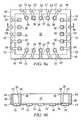
- FIGS. 1 a - 1 billustrate top and side views of a semiconductor wafer having a plurality of die separated by saw street guides
- FIGS. 2 a - 2 billustrate top and side views of the semiconductor wafer with trenches formed in the saw street guides
- FIGS. 3 a - 3 billustrate top and side views of expanding the saw street guides
- FIGS. 4 a - 4 billustrate top and side views of the expanded saw streets filled with organic material
- FIGS. 5 a - 5 billustrate top and side views of forming via holes through the organic material in the saw streets and via holes in an active area of the die;
- FIGS. 7 a - 7 billustrate top and side views of cutting the metal vias on the saw streets into two half-circle vias
- FIGS. 8 a - 8 billustrate top and side views of a semiconductor die with metal vias formed along the saw streets and metal vias formed in the active area of the die;
- FIGS. 9 a - 9 billustrate top and side views of a semiconductor die with redistribution layers formed on a backside of the die
- FIGS. 10 a - 10 billustrate top and side views of two side-by-side metal vias formed along the saw streets
- FIGS. 11 a - 11 billustrate top and side views of cutting the organic material between the two side-by-side metal vias to separate the die
- FIGS. 12 a - 12 billustrate top and side views of a semiconductor die with full-circle vias along the saw streets and vias formed in the active area of the die;
- FIG. 13illustrates die-to-die stacking using direct metal-to-metal via bonding
- FIG. 14illustrates die-to-die stacking using via bonding with solder paste
- FIG. 15illustrates the semiconductor die with metal vias connected to a second die with wire bonds
- FIG. 16illustrates the semiconductor die with metal vias connected to a second die with bond wires and solder bumps
- FIG. 18illustrates another embodiment of interconnecting die using metal vias on saw streets and metal vias in the active area of the die.
- Front-end manufacturinggenerally refers to formation of the semiconductor devices on the wafer.
- the finished waferhas an active side containing the transistors and other active and passive components.
- Back-end manufacturingrefers to cutting or singulating the finished wafer into the individual die and then packaging the die for structural support and/or environmental isolation.
- a semiconductor wafergenerally includes an active front side surface having semiconductor devices disposed thereon, and a backside surface formed with bulk semiconductor material, e.g., silicon.
- the active front side surfacecontains a plurality of semiconductor die.
- the active surfaceis formed by a variety of semiconductor processes, including layering, patterning, doping, and heat treatment.
- semiconductor materialsare grown or deposited on the substrate by techniques involving thermal oxidation, nitridation, chemical vapor deposition, evaporation, and sputtering. Patterning involves the use of photolithography to mask areas of the surface and etch away undesired material to form specific structures.
- the doping processinjects concentrations of dopant material by thermal diffusion or ion implantation.
- the active surfaceis substantially planar and uniform with electrical interconnects, such as bond pads.
- Flip chip semiconductor packages and wafer level chip scale packagesare commonly used with integrated circuits (ICs) demanding high speed, high density, and greater pin count.
- Flip chip style packaginginvolves mounting an active area of the die facedown toward a chip carrier substrate or printed circuit board (PCB).
- the active areacontains active and passive devices, conductive layers, and dielectric layers according to the electrical design of the die.
- the electrical and mechanical interconnectis achieved through a solder bump structure comprising a large number of individual conductive solder bumps or balls.
- the solder bumpsare formed on the bump pads which are disposed on the active area.
- the bump padsconnect to the active circuits by conduction tracks or traces in the active area.
- the solder bumpsare electrically and mechanically connected to the contact pads on the carrier substrate by a solder reflow process.
- the flip chip semiconductor packageprovides a short electrical conduction path from the active devices on the die to conduction tracks on the carrier substrate in order to reduce signal propagation, lower capacitance, and achieve overall better circuit performance.
- a WLPhaving through-hole vias (THV) formed along saw streets.
- the backside of the waferhas redistribution layers (RDL) for interconnect flexibility separated by repassivation layers.
- RDLredistribution layers
- WLP with THV formed along saw streetsare described in U.S. patent application Ser. No. 11/744,657, entitled “Through-Hole Via on Saw Streets”, and further in U.S. patent application Ser. No. 11/768,844, entitled “Package on Package Using Through-Hole Via Die on Saw Streets”, which are incorporated herein by reference.
- a semiconductor wafer 30having a plurality of die 32 .
- the dieare separated by inter die wafer area 36 , commonly known as saw street guides.
- the saw street guidesare routed around the wafer such that there is a saw street on every side of each die on the wafer, i.e., around a perimeter of the die.
- Each die 32has a plurality to contact pads 38 formed on silicon, i.e., formed in an active area of die 32 and not in saw street guides 36 .
- Contact pads 38are made of aluminum, copper, or aluminum/copper alloys. Contact pads 38 electrically connect to active and passive devices through conduction tracks or layers formed on die 32 .
- the contact padscan be disposed side-by-side a first distance from the edge of the die, as shown in FIG. 1 a .
- the contact padscan be offset in multiple rows such that a first row of contact pads are disposed a first distance from the edge of the die, and a second row of contact pads alternating with the first row are disposed a second distance from the edge of the die.
- a solder bump or wire bondwill later be formed to connect to each metal contact pad for electrical and mechanical interconnect to a chip carrier substrate or printed circuit board (PCB).
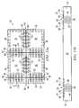
- FIG. 1 bis a cross-sectional view of wafer 30 , taken along line 1 b - 1 b in FIG. 1 a , showing die 32 separated by saw street guides 36 .
- die 32may have dimensions ranging from 2 ⁇ 2 millimeters (mm) to 15 ⁇ 15 mm.
- the saw streetsprovide cutting areas to singulate the wafer into individual die.
- a first die 32is disposed to the left of the leftmost saw street 36 .
- a second die 32is disposed between the saw streets 36 .
- a third die 32is disposed to the right of the rightmost saw street 36 .
- FIG. 2 asemiconductor wafer 30 is again shown with its plurality of die 32 , separated by saw street guides 36 .
- Dicing tape 40is applied to the back of semiconductor wafer 30 for structural support of the wafer during the following manufacturing operations, as shown in FIG. 2 b which is a cross-sectional view taken along line 2 b - 2 b .
- Saw streets 36are cut by cutting tool 44 .
- cutting tool 44can be a saw or laser. Note that the cutting tool completely severs through wafer 30 to form a well or trench 42 .
- the bottom of trench 42is defined by dicing tape 40 .
- the formation of trench 42arises from a first singulation of wafer 30 , which creates a trench width that is less than a width of the channel of saw street guide 36 .
- FIG. 3 asemiconductor wafer 30 is shown with its plurality of die 32 , separated by cut saw street guides 36 .
- Wafer 30undergoes a wafer expansion step to increase the width of saw street guides 36 .
- FIG. 3 bis a cross-sectional view of wafer 30 , taken along line 3 b - 3 b , showing the die being pulled using a wafer expansion table as shown by directional arrows 46 .
- the diecan be picked and placed onto a wafer support system. In any case, the die are positioned farther apart following the steps of FIGS. 3 a - 3 b to create wider saw street guides.
- the die separationincreases from 50 micrometers ( ⁇ m) to 200 ⁇ m.
- the expanded dimensiondepends on the design embodiment, i.e. half via, full via, single row via, or double/multiple row via.
- FIG. 4 asemiconductor wafer 30 is shown with its plurality of die 32 , separated by cut saw street guides 36 .
- Organic material 48is deposited in trench 42 by spin-coating or needle dispensing.
- Organic material 48can be benzocyclobutene (BCB), polyimide (PI), or acrylic resin.
- FIG. 4 bis a cross-sectional view of wafer 30 , taken along line 4 b - 4 b , showing organic material 48 deposited in trench 42 .
- Organic material 48fills trench 42 from dicing tape 40 up to the top surface of die 32 .
- the backside of wafer 30is transferred onto wafer support system 49 , which is made from glass, silicon substrate, or other wafer support material.
- semiconductor wafer 30is shown with its plurality of die 32 , separated by saw street guides 36 filled with organic material 48 .
- a via hole 50is cut into organic material 48 along saw streets 36 .
- the via cutting operationuses a laser drill or etching process.
- Via holes 50are placed along die 32 adjacent to contact pads 38 .
- contact pads 38 and via holes 50have a minimum separation distance of about 20 ⁇ m to 150 ⁇ m, depending on the diameter and depth of the via.
- FIG. 5 bthe cross-sectional view of wafer 30 , taken along line 5 b - 5 b , shows via holes 50 cut into organic material 48 down to wafer support system 49 .
- the laser drilling operationis centered about the channel of the saw street guide and makes a hole having a diameter less than the width of trench 42 , which leaves a layer of organic material 48 surrounding via hole 50 .
- the width of trench 42is dependent on the width of saw street width, but typically smaller than the saw street width.
- the diameter of via hole 50is typically about 10 ⁇ m to 100 ⁇ m, depending on the required via depth.
- via holes 53are cut through contact pads 38 down through wafer 30 to wafer support system 49 .
- the laser drilling operationis centered about contact pad 38 and makes a hole having a diameter less than the width of the contact pad, which leaves part of the contact pad surrounding via hole 53 at the top of die 32 .
- via holes 53are formed on silicon, i.e., through an active area of die 32 .
- a metal track or trace 52is routed from each contact pad 38 to the corresponding via hole 50 .
- Trace 52is formed by a metal patterning process to connect contact pads 38 to via holes 50 , which will be filled with conductive material in a later step. Traces 52 are provided for each contact pad and via hole pairing as shown. Some via holes 50 are dummy vias performing no electrical function. Accordingly, metal trace 52 need not be routed to every via depending on the device function.
- semiconductor wafer 30is shown with its plurality of die 32 , separated by saw street guides 36 with metal-filled vias 54 and 56 .
- a conductive materialis deposited into via holes 50 through a deposition process such as plating or plugging to form metal vias 54 .
- the same conductive materialis also deposited into via holes 53 to form metal vias 56 .
- Metal vias 56are formed through an active area of die 32 .
- the conductive materialcan be copper (Cu), aluminum (Al), tungsten (W), or alloys thereof, or mixtures of other conductive materials.
- Metal vias 54are formed in and are surrounded by organic material 48 .
- Metal vias 56are formed in and are surrounded by contact pad 38 and the active area of wafer 30 .
- Metal via 54electrically connects to contact pad 38 by way of trace 52 . Traces 52 are provided for each contact pad and metal via pairing as shown.
- FIG. 6 bis a cross-sectional view of wafer 30 , taken along line 6 b - 6 b , showing metal vias 54 electrically connecting to contact pads 38 through traces 52 , and metal vias 56 electrically connecting to contact pads 38 directly.
- Wafer support system 49is replaced with dicing tape 58 for structural support of the wafer during the second or final singulation to separate die 32 .
- the bottom of metal vias 54 and 56coincides with dicing tape 58 .
- a redistribution layercan be formed on the backside of wafer 30 .
- the backside RDLoperates as an intermediate conductive layer to route electrical signals to various areas of the die, including active and passive circuits, and provides various electrical interconnect options during package integration, such as shown in FIGS. 15-18 .
- a repassivation layeris formed between the individual nodes of the backside RDL for electrical isolation. The formation of backside RDL and repassivation layer is disclosed in U.S. patent application Ser. No. 11/861,244, entitled “Semiconductor Wafer having Through Hole Vias on Saw Streets with backside redistribution layer.”
- metal vias 54are cut through center area 68 by cutting tool 70 .
- cutting tool 70can be a saw or laser. The cut extends down to dicing tape 58 to completely sever metal vias 54 into two equal half-circle vias 64 .
- a pick and place operationremoves die 32 as individual units from dicing tape 58 .
- FIG. 8 asemiconductor die 32 is shown with both metal vias 64 on saw streets and through silicon metal vias 56 .
- FIG. 8 bis a cross-sectional view of die 32 , taken along line 8 b - 8 b , showing metal vias formed through silicon of die 32 and metal vias on saw street configuration, as produced by the manufacturing steps of FIGS. 1-7 .
- FIG. 9 asemiconductor die 32 is shown with through silicon metal vias 56 and further metal vias 64 on saw streets.
- FIG. 9 bis a cross-sectional view of die 32 , taken along line 9 b - 9 b , showing metal vias formed through silicon of die 32 and metal vias on saw street configuration, as produced by the manufacturing steps of FIGS. 1-7 .
- RDL 74 and repassivation layer 76are shown on the backside of die 32 .
- RDL 74can be made with nickel (Ni), nickel vanadium (NiV), Cu, or Cu alloy.
- RDL 74operates as an intermediate conductive layer to route electrical signals to various areas of the die, including active and passive circuits, and provides various electrical interconnect options during package integration, such as shown in FIGS.
- Repassivation layer 76is formed between the individual nodes of backside RDL 74 for electrical isolation.
- the repassivation layercan be made with silicon nitride (SiN), silicon dioxide (SiO2), silicon oxynitride (SiON), polyimide, benzocyclobutene (BCB), polybenzoxazole (PBO), or other insulating material.
- FIG. 10 asemiconductor die 32 is shown with contact pads 38 connected to metal vias 80 by traces 52 .
- FIG. 10 bis a cross-sectional view of die 32 , taken along line 10 b - 10 b , showing metal vias 80 along saw street 36 .
- the metal viais produced by the steps described in FIGS. 1-7 , with the exception that two via holes like 50 are formed side-by-side in organic material 48 .
- the side-by-side via holes 50are separated by organic material 48 .
- Conductive traces 52connect contact pads 38 and via holes 50 .
- the side-by-side via holesare filled with conductive material to form metal vias 80 .
- semiconductor die 32is shown with contact pads 38 connected to metal vias 80 by traces 52 .
- Dicing tapeis applied to the back of semiconductor wafer 30 for structural support of the wafer during the final singulation to separate die 32 , as shown in FIG. 11 b which is a cross-sectional view taken along line 11 b - 11 b .
- the second or final singulation to separate the plurality of die 32is cut through organic material 48 along line 82 between the side-by-side vias 80 with a cutting tool like 70 .
- the singulation between metal vias 80results in the metal vias on saw street configuration in combination with through silicon vias 56 .
- FIG. 12 asemiconductor die 32 is shown with contact pads 38 connected to metal vias 80 by traces 52 .
- FIG. 12 bis a cross-sectional view of die 32 , taken along line 12 b - 12 b , showing metal vias on saw street configuration.
- the metal full-circle viasare produced by the steps described in FIGS. 1-7 and 10 - 11 .
- the side-by-side via holes like 50are separated by organic material 48 .
- Conductive traces like 52electrically connect the contact pads and via holes.
- the side-by-side via holesare filled with conductive material to form metal vias 80 .
- the final singulation to separate the plurality of die 32is cut through organic material 48 between the side-by-side metal vias 80 resulting in the metal via on saw street configuration in combination with through silicon vias 56 .
- FIG. 13illustrates direct die-to-die stacking using direct via metal bonding.
- a plurality of die 32is stacked as shown to suit a particular application.
- Each of the metal half-vias 64 and through silicon vias 56can be joined together as shown by union 90 using a direct via metal bonding process.
- the combination of vias 64 and 56provide greater interconnect flexibility and options for electrically connecting the stacked die 32 .
- semiconductor die 32 with metal full-vias 80 and through silicon vias 56can be joined together by union 90 using a direct via metal bonding process.
- FIG. 14illustrates die-to-die stacking using via bonding with solder paste 92 .
- a plurality of die 32is stacked as shown to suit a particular application.
- Each of the metal vias 64 and through silicon vias 56can be joined together as shown by reflowing solder paste 92 to create a strong metallurgical bond between each of stacked die 32 .
- the combination of vias 64 and 56provide greater interconnect flexibility and options for electrically connecting the stacked die 32 .
- semiconductor die 32 with metal vias 80 and through silicon vias 56can be joined together by solder paste 92 using a reflow process.
- FIGS. 15-18shows various packaging applications using, in part, an interconnect technique with the THVs formed on saw streets and THVs on silicon.
- FIG. 15has semiconductor die 100 attached to die 32 with adhesive 102 .
- Die 100electrically connects through wire bonds 104 to metal vias 64 on die 32 .
- Die 32is supported by substrate 106 .
- Metal vias 64 and 56electrically connect to solder bumps 108 through conductive layer 110 .
- the packagesare sealed by epoxy encapsulant 112 .
- FIG. 16shows semiconductor die 120 attached to die 122 with adhesive 124 .
- Die 120electrically connects through wire bonds 126 to metal vias 64 on die 32 .
- Die 122electrically connects through solder bumps 128 to metal vias 56 on die 32 .
- Die 32is supported by substrate 130 .
- Metal vias 64 and 56electrically connect to solder bumps 132 through conductive layer 134 .
- the packagesare sealed by epoxy encapsulant 136 .
- FIG. 17shows semiconductor die 140 electrically connected to metal vias 64 or 80 on die 32 by way of bond wires 152 .
- Semiconductor die 154electrically connects to metal vias 64 and 56 on die 32 by way of wire bonds 156 and conductive layer 158 .
- Die 32 and 140are supported by substrate 160 .
- the entire assemblyis mounted to substrate 161 .
- Wire bonds 162 from substrate 160provide the electrical connection to solder bumps 164 through conductive layer 166 .
- the packagesare encased by epoxy encapsulant 168 .
- Molding compound 170encapsulates die 154 .
- FIG. 18shows semiconductor die 180 electrically connected to die 32 with solder bumps 182 .
- Passive devices 184also connect to metal vias 64 with solder paste 186 .
- Die 32is mounted to a semiconductor package containing die 190 with adhesive 192 .
- Die 190electrically connects to solder bumps 200 through wire bonds 194 , conductive layer 196 , and conductive layer 198 .
- the assembly of semiconductor die 32 , 180 , and 190are supported by substrate 202 .
- Metal vias 56electrically connect to solder bumps 200 through wire bonds 204 and conductive layer 198 .
- the packagesare sealed by epoxy encapsulant 206 .
- An underfill material 208provides stress relief.
- stackable semiconductor diehas been described with THVs formed in the saw streets and THVs formed on silicon.
- the electrical interconnectis accomplished using the THVs on saw streets and THVs on silicon, in addition to a redistribution layer, separated by a repassivation layer, to increase signal routing options and density.
- the THVs on saw streets and THVs on silicon, in addition to the RDLs,provide more signal routing functionality and flexibility within the package.
Landscapes
- Engineering & Computer Science (AREA)
- Microelectronics & Electronic Packaging (AREA)
- Power Engineering (AREA)
- Computer Hardware Design (AREA)
- Physics & Mathematics (AREA)
- Condensed Matter Physics & Semiconductors (AREA)
- General Physics & Mathematics (AREA)
- Manufacturing & Machinery (AREA)
- Internal Circuitry In Semiconductor Integrated Circuit Devices (AREA)
Abstract
Description
Claims (15)
Priority Applications (6)
| Application Number | Priority Date | Filing Date | Title |
|---|---|---|---|
| US11/861,251US7902638B2 (en) | 2007-05-04 | 2007-09-25 | Semiconductor die with through-hole via on saw streets and through-hole via in active area of die |
| TW097130210ATWI373110B (en) | 2007-09-25 | 2008-08-08 | Semiconductor die with through-hole via on saw streets and through-hole via in active area of die |
| SG200806002-2ASG151167A1 (en) | 2007-09-25 | 2008-08-13 | Semiconductor die with through-hole via on saw streets and through-hole via in active area of die |
| SG201101669-8ASG170083A1 (en) | 2007-09-25 | 2008-08-13 | Method of fabricating semiconductor die with through-hole via on saw streets and through-hole via in active area of die |
| KR1020080093390AKR101555708B1 (en) | 2007-09-25 | 2008-09-23 | A semiconductor wafer a semiconductor package and a method of making a semiconductor package |
| US13/021,856US8815643B2 (en) | 2007-05-04 | 2011-02-07 | Method of fabricating semiconductor die with through-hole via on saw streets and through-hole via in active area of die |
Applications Claiming Priority (3)
| Application Number | Priority Date | Filing Date | Title |
|---|---|---|---|
| US11/744,657US7569421B2 (en) | 2007-05-04 | 2007-05-04 | Through-hole via on saw streets |
| US11/768,844US7723159B2 (en) | 2007-05-04 | 2007-06-26 | Package-on-package using through-hole via die on saw streets |
| US11/861,251US7902638B2 (en) | 2007-05-04 | 2007-09-25 | Semiconductor die with through-hole via on saw streets and through-hole via in active area of die |
Related Parent Applications (1)
| Application Number | Title | Priority Date | Filing Date |
|---|---|---|---|
| US11/768,844Continuation-In-PartUS7723159B2 (en) | 2007-05-04 | 2007-06-26 | Package-on-package using through-hole via die on saw streets |
Related Child Applications (1)
| Application Number | Title | Priority Date | Filing Date |
|---|---|---|---|
| US13/021,856DivisionUS8815643B2 (en) | 2007-05-04 | 2011-02-07 | Method of fabricating semiconductor die with through-hole via on saw streets and through-hole via in active area of die |
Publications (2)
| Publication Number | Publication Date |
|---|---|
| US20080272465A1 US20080272465A1 (en) | 2008-11-06 |
| US7902638B2true US7902638B2 (en) | 2011-03-08 |
Family
ID=40586523
Family Applications (2)
| Application Number | Title | Priority Date | Filing Date |
|---|---|---|---|
| US11/861,251Active2029-02-11US7902638B2 (en) | 2007-05-04 | 2007-09-25 | Semiconductor die with through-hole via on saw streets and through-hole via in active area of die |
| US13/021,856Active2027-09-25US8815643B2 (en) | 2007-05-04 | 2011-02-07 | Method of fabricating semiconductor die with through-hole via on saw streets and through-hole via in active area of die |
Family Applications After (1)
| Application Number | Title | Priority Date | Filing Date |
|---|---|---|---|
| US13/021,856Active2027-09-25US8815643B2 (en) | 2007-05-04 | 2011-02-07 | Method of fabricating semiconductor die with through-hole via on saw streets and through-hole via in active area of die |
Country Status (4)
| Country | Link |
|---|---|
| US (2) | US7902638B2 (en) |
| KR (1) | KR101555708B1 (en) |
| SG (2) | SG151167A1 (en) |
| TW (1) | TWI373110B (en) |
Cited By (12)
| Publication number | Priority date | Publication date | Assignee | Title |
|---|---|---|---|---|
| US20100321822A1 (en)* | 2009-06-19 | 2010-12-23 | Tdk Corporation | Manufacturing method of thin-film magnetic head, wafer for thin-film magnetic head and thin-film magnetic head |
| US20110062592A1 (en)* | 2009-09-11 | 2011-03-17 | Taiwan Semiconductor Manufacturing Company, Ltd. | Delamination Resistance of Stacked Dies in Die Saw |
| US20110076804A1 (en)* | 2007-11-21 | 2011-03-31 | Jong Man-Kyo | Power device packages and methods of fabricating the same |
| US20130032952A1 (en)* | 2011-08-01 | 2013-02-07 | Stats Chippac, Ltd. | Semiconductor Device and Method of Forming POP With Stacked Semiconductor Die and Bumps Formed Directly on the Lower Die |
| US8664768B2 (en)* | 2012-05-03 | 2014-03-04 | Taiwan Semiconductor Manufacturing Company, Ltd. | Interposer having a defined through via pattern |
| US9418876B2 (en) | 2011-09-02 | 2016-08-16 | Taiwan Semiconductor Manufacturing Company, Ltd. | Method of three dimensional integrated circuit assembly |
| US9691634B2 (en) | 2015-04-02 | 2017-06-27 | Abexl Inc. | Method for creating through-connected vias and conductors on a substrate |
| US9859181B2 (en) | 2011-09-02 | 2018-01-02 | Taiwan Semiconductor Manufacturing Company, Ltd. | Underfill dispensing in 3D IC using metrology |
| US10593562B2 (en) | 2015-04-02 | 2020-03-17 | Samtec, Inc. | Method for creating through-connected vias and conductors on a substrate |
| US11424212B2 (en)* | 2019-07-17 | 2022-08-23 | Advanced Semiconductor Engineering, Inc. | Semiconductor package structure and method for manufacturing the same |
| US12009225B2 (en) | 2018-03-30 | 2024-06-11 | Samtec, Inc. | Electrically conductive vias and methods for producing same |
| US12100647B2 (en) | 2019-09-30 | 2024-09-24 | Samtec, Inc. | Electrically conductive vias and methods for producing same |
Families Citing this family (39)
| Publication number | Priority date | Publication date | Assignee | Title |
|---|---|---|---|---|
| US7972902B2 (en) | 2007-07-23 | 2011-07-05 | Samsung Electronics Co., Ltd. | Method of manufacturing a wafer including providing electrical conductors isolated from circuitry |
| KR101185886B1 (en) | 2007-07-23 | 2012-09-25 | 삼성전자주식회사 | Semiconductor chip, semiconductor package, card and system having universal interconnection lines |
| KR101465948B1 (en)* | 2007-12-27 | 2014-12-10 | 삼성전자주식회사 | A wafer level stack package and method of manufacturing a wafer level stack package |
| US8072079B2 (en) | 2008-03-27 | 2011-12-06 | Stats Chippac, Ltd. | Through hole vias at saw streets including protrusions or recesses for interconnection |
| US7704796B2 (en)* | 2008-06-04 | 2010-04-27 | Stats Chippac, Ltd. | Semiconductor device and method of forming recessed conductive vias in saw streets |
| US8021907B2 (en)* | 2008-06-09 | 2011-09-20 | Stats Chippac, Ltd. | Method and apparatus for thermally enhanced semiconductor package |
| US7888184B2 (en)* | 2008-06-20 | 2011-02-15 | Stats Chippac Ltd. | Integrated circuit packaging system with embedded circuitry and post, and method of manufacture thereof |
| US8080885B2 (en)* | 2008-11-19 | 2011-12-20 | Stats Chippac Ltd. | Integrated circuit packaging system with multi level contact and method of manufacture thereof |
| US7982298B1 (en)* | 2008-12-03 | 2011-07-19 | Amkor Technology, Inc. | Package in package semiconductor device |
| US8093711B2 (en)* | 2009-02-02 | 2012-01-10 | Infineon Technologies Ag | Semiconductor device |
| KR20100096879A (en)* | 2009-02-25 | 2010-09-02 | 삼성전자주식회사 | Devices including copper pads, stacked structures thereof and methods of manufacturing the same |
| US20110068478A1 (en)* | 2009-03-26 | 2011-03-24 | Reza Argenty Pagaila | Integrated circuit packaging system with package stacking and method of manufacture thereof |
| US7847382B2 (en)* | 2009-03-26 | 2010-12-07 | Stats Chippac Ltd. | Integrated circuit packaging system with package stacking and method of manufacture thereof |
| US20100270668A1 (en)* | 2009-04-28 | 2010-10-28 | Wafer-Level Packaging Portfolio Llc | Dual Interconnection in Stacked Memory and Controller Module |
| US8587129B2 (en)* | 2009-07-31 | 2013-11-19 | Stats Chippac Ltd. | Integrated circuit packaging system with through silicon via base and method of manufacture thereof |
| US7867821B1 (en)* | 2009-09-18 | 2011-01-11 | Stats Chippac Ltd. | Integrated circuit package system with through semiconductor vias and method of manufacture thereof |
| US8822281B2 (en)* | 2010-02-23 | 2014-09-02 | Stats Chippac, Ltd. | Semiconductor device and method of forming TMV and TSV in WLCSP using same carrier |
| EP2543065A4 (en) | 2010-03-03 | 2018-01-24 | Georgia Tech Research Corporation | Through-package-via (tpv) structures on inorganic interposer and methods for fabricating same |
| US20120007211A1 (en)* | 2010-07-06 | 2012-01-12 | Aleksandar Aleksov | In-street die-to-die interconnects |
| KR101683814B1 (en) | 2010-07-26 | 2016-12-08 | 삼성전자주식회사 | Semiconductor apparatus having through vias |
| DE102010041129A1 (en)* | 2010-09-21 | 2012-03-22 | Robert Bosch Gmbh | Multifunction sensor as PoP mWLP |
| WO2012069078A1 (en)* | 2010-11-23 | 2012-05-31 | Robert Bosch Gmbh | Eutectic bonding of thin chips on a carrier substrate |
| US8883561B2 (en) | 2011-04-30 | 2014-11-11 | Stats Chippac, Ltd. | Semiconductor device and method of embedding TSV semiconductor die within encapsulant with TMV for vertical interconnect in POP |
| US9704725B1 (en) | 2012-03-06 | 2017-07-11 | Amkor Technology, Inc. | Semiconductor device with leadframe configured to facilitate reduced burr formation |
| US9136213B2 (en) | 2012-08-02 | 2015-09-15 | Infineon Technologies Ag | Integrated system and method of making the integrated system |
| KR101486790B1 (en) | 2013-05-02 | 2015-01-28 | 앰코 테크놀로지 코리아 주식회사 | Micro Lead Frame for semiconductor package |
| KR102053349B1 (en) | 2013-05-16 | 2019-12-06 | 삼성전자주식회사 | Semiconductor package |
| KR101563911B1 (en) | 2013-10-24 | 2015-10-28 | 앰코 테크놀로지 코리아 주식회사 | Semiconductor package |
| US9524942B2 (en)* | 2013-12-18 | 2016-12-20 | Taiwan Semiconductor Manufacturing Company, Ltd. | Chip-on-substrate packaging on carrier |
| US9196592B2 (en) | 2014-01-10 | 2015-11-24 | International Business Machines Corporation | Methods of managing metal density in dicing channel and related integrated circuit structures |
| US9610543B2 (en) | 2014-01-31 | 2017-04-04 | Infineon Technologies Ag | Method for simultaneous structuring and chip singulation |
| US9673122B2 (en) | 2014-05-02 | 2017-06-06 | Amkor Technology, Inc. | Micro lead frame structure having reinforcing portions and method |
| US12087629B2 (en) | 2015-05-18 | 2024-09-10 | Adeia Semiconductor Technologies Llc | Through-dielectric-vias (TDVs) for 3D integrated circuits in silicon |
| KR102470168B1 (en)* | 2015-12-08 | 2022-11-23 | 삼성전기주식회사 | Package substrate |
| CN107686092A (en)* | 2016-08-04 | 2018-02-13 | 北京卓锐微技术有限公司 | Crystal circle structure and wafer processing method |
| KR102532205B1 (en) | 2018-07-09 | 2023-05-12 | 삼성전자 주식회사 | Semiconductor chip and Semiconductor Package comprising the semiconductor chip |
| CN111682003B (en)* | 2019-03-11 | 2024-04-19 | 奥特斯奥地利科技与系统技术有限公司 | Component carrier comprising a component with a vertical through connection |
| US11456289B2 (en) | 2019-12-27 | 2022-09-27 | Micron Technology, Inc. | Face-to-face semiconductor device with fan-out porch |
| US20210375845A1 (en)* | 2020-05-27 | 2021-12-02 | Qualcomm Incorporated | Package cavity for enhanced device performance with an integrated passive device |
Citations (9)
| Publication number | Priority date | Publication date | Assignee | Title |
|---|---|---|---|---|
| US5694551A (en) | 1993-05-20 | 1997-12-02 | Moore Business Forms, Inc. | Computer integration network for channeling customer orders through a centralized computer to various suppliers |
| US6157915A (en) | 1998-08-07 | 2000-12-05 | International Business Machines Corporation | Method and apparatus for collaboratively managing supply chains |
| US20020013721A1 (en) | 2000-05-22 | 2002-01-31 | Alan Dabbiere | System, method and apparatus for integrated supply chain management |
| US20020019761A1 (en) | 2000-01-12 | 2002-02-14 | Derek Lidow | Supply chain architecture |
| US20020042755A1 (en) | 2000-10-05 | 2002-04-11 | I2 Technologies, Us, Inc. | Collaborative fulfillment in a distributed supply chain environment |
| US20020049622A1 (en) | 2000-04-27 | 2002-04-25 | Lettich Anthony R. | Vertical systems and methods for providing shipping and logistics services, operations and products to an industry |
| US6400008B1 (en)* | 1996-02-16 | 2002-06-04 | Micron Technology, Inc. | Surface mount ic using silicon vias in an area array format or same size as die array |
| US6743696B2 (en) | 2001-10-16 | 2004-06-01 | Micron Technology, Inc. | Apparatus and method for leadless packaging of semiconductor devices |
| US20050186705A1 (en)* | 2002-07-31 | 2005-08-25 | Jackson Timothy L. | Semiconductor dice having backside redistribution layer accessed using through-silicon vias, methods |
Family Cites Families (6)
| Publication number | Priority date | Publication date | Assignee | Title |
|---|---|---|---|---|
| US7506438B1 (en)* | 2000-11-14 | 2009-03-24 | Freescale Semiconductor, Inc. | Low profile integrated module interconnects and method of fabrication |
| US6943056B2 (en)* | 2002-04-16 | 2005-09-13 | Renesas Technology Corp. | Semiconductor device manufacturing method and electronic equipment using same |
| DE10250621B4 (en)* | 2002-10-30 | 2004-09-02 | Fraunhofer-Gesellschaft zur Förderung der angewandten Forschung e.V. | A method of producing encapsulated chips and generating a stack of the encapsulated chips |
| JP2004221372A (en) | 2003-01-16 | 2004-08-05 | Seiko Epson Corp | Semiconductor device, semiconductor module, electronic device, method of manufacturing semiconductor device, and method of manufacturing semiconductor module |
| KR100575591B1 (en)* | 2004-07-27 | 2006-05-03 | 삼성전자주식회사 | Chip scale package for wafer level stack package and manufacturing method thereof |
| US7199449B2 (en)* | 2004-08-24 | 2007-04-03 | Micron Technology, Inc. | Wafer backside removal to complete through-holes and provide wafer singulation during the formation of a semiconductor device |
- 2007
- 2007-09-25USUS11/861,251patent/US7902638B2/enactiveActive
- 2008
- 2008-08-08TWTW097130210Apatent/TWI373110B/enactive
- 2008-08-13SGSG200806002-2Apatent/SG151167A1/enunknown
- 2008-08-13SGSG201101669-8Apatent/SG170083A1/enunknown
- 2008-09-23KRKR1020080093390Apatent/KR101555708B1/enactiveActive
- 2011
- 2011-02-07USUS13/021,856patent/US8815643B2/enactiveActive
Patent Citations (9)
| Publication number | Priority date | Publication date | Assignee | Title |
|---|---|---|---|---|
| US5694551A (en) | 1993-05-20 | 1997-12-02 | Moore Business Forms, Inc. | Computer integration network for channeling customer orders through a centralized computer to various suppliers |
| US6400008B1 (en)* | 1996-02-16 | 2002-06-04 | Micron Technology, Inc. | Surface mount ic using silicon vias in an area array format or same size as die array |
| US6157915A (en) | 1998-08-07 | 2000-12-05 | International Business Machines Corporation | Method and apparatus for collaboratively managing supply chains |
| US20020019761A1 (en) | 2000-01-12 | 2002-02-14 | Derek Lidow | Supply chain architecture |
| US20020049622A1 (en) | 2000-04-27 | 2002-04-25 | Lettich Anthony R. | Vertical systems and methods for providing shipping and logistics services, operations and products to an industry |
| US20020013721A1 (en) | 2000-05-22 | 2002-01-31 | Alan Dabbiere | System, method and apparatus for integrated supply chain management |
| US20020042755A1 (en) | 2000-10-05 | 2002-04-11 | I2 Technologies, Us, Inc. | Collaborative fulfillment in a distributed supply chain environment |
| US6743696B2 (en) | 2001-10-16 | 2004-06-01 | Micron Technology, Inc. | Apparatus and method for leadless packaging of semiconductor devices |
| US20050186705A1 (en)* | 2002-07-31 | 2005-08-25 | Jackson Timothy L. | Semiconductor dice having backside redistribution layer accessed using through-silicon vias, methods |
Cited By (19)
| Publication number | Priority date | Publication date | Assignee | Title |
|---|---|---|---|---|
| US20110076804A1 (en)* | 2007-11-21 | 2011-03-31 | Jong Man-Kyo | Power device packages and methods of fabricating the same |
| US8098462B2 (en)* | 2009-06-19 | 2012-01-17 | Tdk Corporation | Manufacturing method of thin-film magnetic head, wafer for thin-film magnetic head and thin-film magnetic head |
| US20100321822A1 (en)* | 2009-06-19 | 2010-12-23 | Tdk Corporation | Manufacturing method of thin-film magnetic head, wafer for thin-film magnetic head and thin-film magnetic head |
| US20110062592A1 (en)* | 2009-09-11 | 2011-03-17 | Taiwan Semiconductor Manufacturing Company, Ltd. | Delamination Resistance of Stacked Dies in Die Saw |
| US8803332B2 (en)* | 2009-09-11 | 2014-08-12 | Taiwan Semiconductor Manufacturing Company, Ltd. | Delamination resistance of stacked dies in die saw |
| US9324659B2 (en)* | 2011-08-01 | 2016-04-26 | Stats Chippac, Ltd. | Semiconductor device and method of forming POP with stacked semiconductor die and bumps formed directly on the lower die |
| US20130032952A1 (en)* | 2011-08-01 | 2013-02-07 | Stats Chippac, Ltd. | Semiconductor Device and Method of Forming POP With Stacked Semiconductor Die and Bumps Formed Directly on the Lower Die |
| US9418876B2 (en) | 2011-09-02 | 2016-08-16 | Taiwan Semiconductor Manufacturing Company, Ltd. | Method of three dimensional integrated circuit assembly |
| US9859181B2 (en) | 2011-09-02 | 2018-01-02 | Taiwan Semiconductor Manufacturing Company, Ltd. | Underfill dispensing in 3D IC using metrology |
| US8664768B2 (en)* | 2012-05-03 | 2014-03-04 | Taiwan Semiconductor Manufacturing Company, Ltd. | Interposer having a defined through via pattern |
| US9460989B2 (en) | 2012-05-03 | 2016-10-04 | Taiwan Semiconductor Manufacturing Company, Ltd. | Interposer having a defined through via pattern |
| US9691634B2 (en) | 2015-04-02 | 2017-06-27 | Abexl Inc. | Method for creating through-connected vias and conductors on a substrate |
| US10593562B2 (en) | 2015-04-02 | 2020-03-17 | Samtec, Inc. | Method for creating through-connected vias and conductors on a substrate |
| US10727084B2 (en) | 2015-04-02 | 2020-07-28 | Samtec, Inc. | Method for creating through-connected vias and conductors on a substrate |
| US11107702B2 (en) | 2015-04-02 | 2021-08-31 | Samtec, Inc. | Method for creating through-connected vias and conductors on a substrate |
| US12009225B2 (en) | 2018-03-30 | 2024-06-11 | Samtec, Inc. | Electrically conductive vias and methods for producing same |
| US11424212B2 (en)* | 2019-07-17 | 2022-08-23 | Advanced Semiconductor Engineering, Inc. | Semiconductor package structure and method for manufacturing the same |
| US12040312B2 (en) | 2019-07-17 | 2024-07-16 | Advanced Semiconductor Engineering, Inc. | Semiconductor package structure and method for manufacturing the same |
| US12100647B2 (en) | 2019-09-30 | 2024-09-24 | Samtec, Inc. | Electrically conductive vias and methods for producing same |
Also Published As
| Publication number | Publication date |
|---|---|
| US8815643B2 (en) | 2014-08-26 |
| KR101555708B1 (en) | 2015-09-25 |
| US20120244661A9 (en) | 2012-09-27 |
| KR20090031829A (en) | 2009-03-30 |
| SG151167A1 (en) | 2009-04-30 |
| TW200915509A (en) | 2009-04-01 |
| US20110124156A1 (en) | 2011-05-26 |
| SG170083A1 (en) | 2011-04-29 |
| TWI373110B (en) | 2012-09-21 |
| US20080272465A1 (en) | 2008-11-06 |
Similar Documents
| Publication | Publication Date | Title |
|---|---|---|
| US7902638B2 (en) | Semiconductor die with through-hole via on saw streets and through-hole via in active area of die | |
| US7829998B2 (en) | Semiconductor wafer having through-hole vias on saw streets with backside redistribution layer | |
| US7585750B2 (en) | Semiconductor package having through-hole via on saw streets formed with partial saw | |
| US9331002B2 (en) | Semiconductor device and method of forming through vias with reflowed conductive material | |
| US8557639B2 (en) | Apparatus for thermally enhanced semiconductor package | |
| US7666711B2 (en) | Semiconductor device and method of forming double-sided through vias in saw streets | |
| US8525344B2 (en) | Semiconductor device and method of forming bond wires between semiconductor die contact pads and conductive TOV in peripheral area around semiconductor die | |
| US8072079B2 (en) | Through hole vias at saw streets including protrusions or recesses for interconnection | |
| US9252075B2 (en) | Semiconductor device and method of forming a conductive via-in-via structure | |
| US9601369B2 (en) | Semiconductor device and method of forming conductive vias with trench in saw street | |
| US20100007029A1 (en) | Semiconductor device and method of forming stepped-down rdl and recessed thv in peripheral region of the device |
Legal Events
| Date | Code | Title | Description |
|---|---|---|---|
| AS | Assignment | Owner name:STATS CHIPPAC, LTD., SINGAPORE Free format text:ASSIGNMENT OF ASSIGNORS INTEREST;ASSIGNORS:DO, BYUNG TAI;KUAN, HEAP HOE;CHUA, LINDA PEI EE;REEL/FRAME:019876/0423 Effective date:20070924 | |
| STCF | Information on status: patent grant | Free format text:PATENTED CASE | |
| FPAY | Fee payment | Year of fee payment:4 | |
| AS | Assignment | Owner name:CITICORP INTERNATIONAL LIMITED, AS COMMON SECURITY AGENT, HONG KONG Free format text:SECURITY INTEREST;ASSIGNORS:STATS CHIPPAC, INC.;STATS CHIPPAC LTD.;REEL/FRAME:036288/0748 Effective date:20150806 Owner name:CITICORP INTERNATIONAL LIMITED, AS COMMON SECURITY Free format text:SECURITY INTEREST;ASSIGNORS:STATS CHIPPAC, INC.;STATS CHIPPAC LTD.;REEL/FRAME:036288/0748 Effective date:20150806 | |
| AS | Assignment | Owner name:STATS CHIPPAC PTE. LTE., SINGAPORE Free format text:CHANGE OF NAME;ASSIGNOR:STATS CHIPPAC LTD.;REEL/FRAME:038378/0292 Effective date:20160329 | |
| MAFP | Maintenance fee payment | Free format text:PAYMENT OF MAINTENANCE FEE, 8TH YEAR, LARGE ENTITY (ORIGINAL EVENT CODE: M1552); ENTITY STATUS OF PATENT OWNER: LARGE ENTITY Year of fee payment:8 | |
| AS | Assignment | Owner name:STATS CHIPPAC PTE. LTD. FORMERLY KNOWN AS STATS CH Free format text:RELEASE BY SECURED PARTY;ASSIGNOR:CITICORP INTERNATIONAL LIMITED, AS COMMON SECURITY AGENT;REEL/FRAME:051285/0318 Effective date:20190503 Owner name:STATS CHIPPAC, INC., CALIFORNIA Free format text:RELEASE BY SECURED PARTY;ASSIGNOR:CITICORP INTERNATIONAL LIMITED, AS COMMON SECURITY AGENT;REEL/FRAME:051285/0318 Effective date:20190503 Owner name:STATS CHIPPAC PTE. LTD. FORMERLY KNOWN AS STATS CHIPPAC LTD., SINGAPORE Free format text:RELEASE BY SECURED PARTY;ASSIGNOR:CITICORP INTERNATIONAL LIMITED, AS COMMON SECURITY AGENT;REEL/FRAME:051285/0318 Effective date:20190503 | |
| AS | Assignment | Owner name:JCET SEMICONDUCTOR (SHAOXING) CO., LTD., CHINA Free format text:ASSIGNMENT OF ASSIGNORS INTEREST;ASSIGNOR:STATS CHIPPAC PTE. LTD.;REEL/FRAME:051365/0680 Effective date:20191128 | |
| MAFP | Maintenance fee payment | Free format text:PAYMENT OF MAINTENANCE FEE, 12TH YEAR, LARGE ENTITY (ORIGINAL EVENT CODE: M1553); ENTITY STATUS OF PATENT OWNER: LARGE ENTITY Year of fee payment:12 | |
| AS | Assignment | Owner name:STATS CHIPPAC PTE.LTE., SINGAPORE Free format text:CORRECT ERROR IN ASSIGNMENT NAME FROM STATS CHIPPAC PTE. LTE. TO STATS CHIPPAC PTE. LTD. (REEL: 038378 FRAME: 0292);ASSIGNOR:STATS CHIPPAC LTD.;REEL/FRAME:064783/0896 Effective date:20160329 | |
| AS | Assignment | Owner name:STATS CHIPPAC PTE. LTD., SINGAPORE Free format text:CORRECTIVE ASSIGNMENT TO CORRECT THE ASSIGNEE'S NAME ON COVERSHEET FROM STATS CHIPPAC PTE. LTE. TO STATS CHIPPAC PTE. LTD. PREVIOUSLY RECORDED ON REEL 038378 FRAME 0292. ASSIGNOR(S) HEREBY CONFIRMS THE CHANGE OF NAME;ASSIGNOR:STATS CHIPPAC LTD.;REEL/FRAME:064962/0123 Effective date:20160329 | |
| AS | Assignment | Owner name:STATS CHIPPAC PTE. LTD., SINGAPORE Free format text:CORRECTIVE ASSIGNMENT TO CORRECT THE ASSIGNEE'S NAME ON COVER SHEET FROM STATS CHIPPAC PTE. LTE. TO STATS CHIPPAC PTE. LTD. PREVIOUSLY RECORDED ON REEL 064783 FRAME 0896. ASSIGNOR(S) HEREBY CONFIRMS THE CORRECTIVE CHANGE OF NAME;ASSIGNOR:STATS CHIPPAC LTD.;REEL/FRAME:065015/0917 Effective date:20160329 |