US7902075B2 - Semiconductor trench structure having a sealing plug and method - Google Patents
Semiconductor trench structure having a sealing plug and methodDownload PDFInfo
- Publication number
- US7902075B2 US7902075B2US12/206,541US20654108AUS7902075B2US 7902075 B2US7902075 B2US 7902075B2US 20654108 AUS20654108 AUS 20654108AUS 7902075 B2US7902075 B2US 7902075B2
- Authority
- US
- United States
- Prior art keywords
- trench
- dielectric layer
- layer
- forming
- layers
- Prior art date
- Legal status (The legal status is an assumption and is not a legal conclusion. Google has not performed a legal analysis and makes no representation as to the accuracy of the status listed.)
- Active, expires
Links
- 239000004065semiconductorSubstances0.000titleclaimsabstractdescription111
- 238000000034methodMethods0.000titleclaimsdescription57
- 238000007789sealingMethods0.000titleclaimsdescription7
- 239000000463materialSubstances0.000claimsdescription73
- VYPSYNLAJGMNEJ-UHFFFAOYSA-NSilicium dioxideChemical compoundO=[Si]=OVYPSYNLAJGMNEJ-UHFFFAOYSA-N0.000claimsdescription16
- 229910052581Si3N4Inorganic materials0.000claimsdescription11
- HQVNEWCFYHHQES-UHFFFAOYSA-Nsilicon nitrideChemical compoundN12[Si]34N5[Si]62N3[Si]51N64HQVNEWCFYHHQES-UHFFFAOYSA-N0.000claimsdescription11
- 239000013078crystalSubstances0.000claimsdescription10
- 238000005530etchingMethods0.000claimsdescription9
- 229910052814silicon oxideInorganic materials0.000claimsdescription8
- 230000000873masking effectEffects0.000claimsdescription3
- 239000010410layerSubstances0.000description281
- 239000002019doping agentSubstances0.000description33
- 210000000746body regionAnatomy0.000description28
- 238000002955isolationMethods0.000description20
- 125000004429atomChemical group0.000description17
- 230000008569processEffects0.000description17
- 230000015572biosynthetic processEffects0.000description14
- 239000007789gasSubstances0.000description14
- 239000007943implantSubstances0.000description14
- 229910021420polycrystalline siliconInorganic materials0.000description14
- 238000012545processingMethods0.000description14
- 239000000758substrateSubstances0.000description14
- MROCJMGDEKINLD-UHFFFAOYSA-NdichlorosilaneChemical compoundCl[SiH2]ClMROCJMGDEKINLD-UHFFFAOYSA-N0.000description13
- 229920005591polysiliconPolymers0.000description13
- 230000007547defectEffects0.000description12
- XUIMIQQOPSSXEZ-UHFFFAOYSA-NSiliconChemical compound[Si]XUIMIQQOPSSXEZ-UHFFFAOYSA-N0.000description11
- 238000004519manufacturing processMethods0.000description11
- 229910052710siliconInorganic materials0.000description11
- 239000010703siliconSubstances0.000description11
- 238000000708deep reactive-ion etchingMethods0.000description8
- 239000001257hydrogenSubstances0.000description8
- 229910052739hydrogenInorganic materials0.000description8
- 229920002120photoresistant polymerPolymers0.000description8
- 230000003071parasitic effectEffects0.000description7
- UFHFLCQGNIYNRP-UHFFFAOYSA-NHydrogenChemical compound[H][H]UFHFLCQGNIYNRP-UHFFFAOYSA-N0.000description6
- BLRPTPMANUNPDV-UHFFFAOYSA-NSilaneChemical compound[SiH4]BLRPTPMANUNPDV-UHFFFAOYSA-N0.000description6
- 239000011229interlayerSubstances0.000description6
- 229910000077silaneInorganic materials0.000description6
- 238000000151depositionMethods0.000description5
- 238000013461designMethods0.000description5
- 239000003989dielectric materialSubstances0.000description5
- PZPGRFITIJYNEJ-UHFFFAOYSA-NdisilaneChemical compound[SiH3][SiH3]PZPGRFITIJYNEJ-UHFFFAOYSA-N0.000description5
- ZDHXKXAHOVTTAH-UHFFFAOYSA-NtrichlorosilaneChemical compoundCl[SiH](Cl)ClZDHXKXAHOVTTAH-UHFFFAOYSA-N0.000description5
- 239000005052trichlorosilaneSubstances0.000description5
- 230000004888barrier functionEffects0.000description4
- 229910052796boronInorganic materials0.000description4
- 230000001413cellular effectEffects0.000description4
- BHEPBYXIRTUNPN-UHFFFAOYSA-Nhydridophosphorus(.) (triplet)Chemical compound[PH]BHEPBYXIRTUNPN-UHFFFAOYSA-N0.000description4
- 235000012239silicon dioxideNutrition0.000description4
- 239000000377silicon dioxideSubstances0.000description4
- 125000006850spacer groupChemical group0.000description4
- 229910052785arsenicInorganic materials0.000description3
- RQNWIZPPADIBDY-UHFFFAOYSA-Narsenic atomChemical compound[As]RQNWIZPPADIBDY-UHFFFAOYSA-N0.000description3
- 239000000969carrierSubstances0.000description3
- 230000015556catabolic processEffects0.000description3
- 239000000356contaminantSubstances0.000description3
- 238000007796conventional methodMethods0.000description3
- 230000000694effectsEffects0.000description3
- 230000005684electric fieldEffects0.000description3
- 230000001965increasing effectEffects0.000description3
- ZOXJGFHDIHLPTG-UHFFFAOYSA-NBoronChemical compound[B]ZOXJGFHDIHLPTG-UHFFFAOYSA-N0.000description2
- ZAMOUSCENKQFHK-UHFFFAOYSA-NChlorine atomChemical compound[Cl]ZAMOUSCENKQFHK-UHFFFAOYSA-N0.000description2
- 239000004593EpoxySubstances0.000description2
- PXGOKWXKJXAPGV-UHFFFAOYSA-NFluorineChemical compoundFFPXGOKWXKJXAPGV-UHFFFAOYSA-N0.000description2
- 208000012868OvergrowthDiseases0.000description2
- 229910000676Si alloyInorganic materials0.000description2
- 229910000577Silicon-germaniumInorganic materials0.000description2
- GWEVSGVZZGPLCZ-UHFFFAOYSA-NTitan oxideChemical compoundO=[Ti]=OGWEVSGVZZGPLCZ-UHFFFAOYSA-N0.000description2
- RTAQQCXQSZGOHL-UHFFFAOYSA-NTitaniumChemical compound[Ti]RTAQQCXQSZGOHL-UHFFFAOYSA-N0.000description2
- NRTOMJZYCJJWKI-UHFFFAOYSA-NTitanium nitrideChemical compound[Ti]#NNRTOMJZYCJJWKI-UHFFFAOYSA-N0.000description2
- AXQKVSDUCKWEKE-UHFFFAOYSA-N[C].[Ge].[Si]Chemical compound[C].[Ge].[Si]AXQKVSDUCKWEKE-UHFFFAOYSA-N0.000description2
- LEVVHYCKPQWKOP-UHFFFAOYSA-N[Si].[Ge]Chemical compound[Si].[Ge]LEVVHYCKPQWKOP-UHFFFAOYSA-N0.000description2
- QQMBHAVGDGCSGY-UHFFFAOYSA-N[Ti].[Ni].[Ag]Chemical compound[Ti].[Ni].[Ag]QQMBHAVGDGCSGY-UHFFFAOYSA-N0.000description2
- CSDREXVUYHZDNP-UHFFFAOYSA-NalumanylidynesiliconChemical compound[Al].[Si]CSDREXVUYHZDNP-UHFFFAOYSA-N0.000description2
- 238000013459approachMethods0.000description2
- 239000003990capacitorSubstances0.000description2
- 229910052801chlorineInorganic materials0.000description2
- 239000000460chlorineSubstances0.000description2
- 239000004020conductorSubstances0.000description2
- 238000011109contaminationMethods0.000description2
- 230000003247decreasing effectEffects0.000description2
- 238000009792diffusion processMethods0.000description2
- 238000001312dry etchingMethods0.000description2
- 230000005669field effectEffects0.000description2
- 229910052731fluorineInorganic materials0.000description2
- 239000011737fluorineSubstances0.000description2
- 239000010931goldSubstances0.000description2
- 229910052737goldInorganic materials0.000description2
- 238000010438heat treatmentMethods0.000description2
- 150000002431hydrogenChemical class0.000description2
- 238000010348incorporationMethods0.000description2
- 238000005468ion implantationMethods0.000description2
- 239000011159matrix materialSubstances0.000description2
- 229910052751metalInorganic materials0.000description2
- 239000002184metalSubstances0.000description2
- 238000012986modificationMethods0.000description2
- 230000004048modificationEffects0.000description2
- 150000004767nitridesChemical class0.000description2
- 239000011343solid materialSubstances0.000description2
- 239000000126substanceSubstances0.000description2
- 239000010936titaniumSubstances0.000description2
- 229910052719titaniumInorganic materials0.000description2
- 238000012876topographyMethods0.000description2
- 239000011800void materialSubstances0.000description2
- 230000004913activationEffects0.000description1
- 229910052787antimonyInorganic materials0.000description1
- WATWJIUSRGPENY-UHFFFAOYSA-Nantimony atomChemical compound[Sb]WATWJIUSRGPENY-UHFFFAOYSA-N0.000description1
- HAYXDMNJJFVXCI-UHFFFAOYSA-Narsenic(5+)Chemical compound[As+5]HAYXDMNJJFVXCI-UHFFFAOYSA-N0.000description1
- 229910052454barium strontium titanateInorganic materials0.000description1
- 230000008901benefitEffects0.000description1
- 230000000903blocking effectEffects0.000description1
- 150000001638boronChemical class0.000description1
- -1boron ionChemical class0.000description1
- 238000004140cleaningMethods0.000description1
- 230000000295complement effectEffects0.000description1
- 230000006735deficitEffects0.000description1
- 230000001419dependent effectEffects0.000description1
- 238000011982device technologyMethods0.000description1
- BUMGIEFFCMBQDG-UHFFFAOYSA-NdichlorosiliconChemical compoundCl[Si]ClBUMGIEFFCMBQDG-UHFFFAOYSA-N0.000description1
- 230000001939inductive effectEffects0.000description1
- BPUBBGLMJRNUCC-UHFFFAOYSA-Noxygen(2-);tantalum(5+)Chemical compound[O-2].[O-2].[O-2].[O-2].[O-2].[Ta+5].[Ta+5]BPUBBGLMJRNUCC-UHFFFAOYSA-N0.000description1
- 238000002360preparation methodMethods0.000description1
- 230000035882stressEffects0.000description1
- PBCFLUZVCVVTBY-UHFFFAOYSA-Ntantalum pentoxideInorganic materialsO=[Ta](=O)O[Ta](=O)=OPBCFLUZVCVVTBY-UHFFFAOYSA-N0.000description1
- 239000004408titanium dioxideSubstances0.000description1
Images


Classifications
- H—ELECTRICITY
- H10—SEMICONDUCTOR DEVICES; ELECTRIC SOLID-STATE DEVICES NOT OTHERWISE PROVIDED FOR
- H10D—INORGANIC ELECTRIC SEMICONDUCTOR DEVICES
- H10D30/00—Field-effect transistors [FET]
- H10D30/60—Insulated-gate field-effect transistors [IGFET]
- H10D30/64—Double-diffused metal-oxide semiconductor [DMOS] FETs
- H10D30/66—Vertical DMOS [VDMOS] FETs
- H10D30/668—Vertical DMOS [VDMOS] FETs having trench gate electrodes, e.g. UMOS transistors
- H—ELECTRICITY
- H01—ELECTRIC ELEMENTS
- H01L—SEMICONDUCTOR DEVICES NOT COVERED BY CLASS H10
- H01L21/00—Processes or apparatus adapted for the manufacture or treatment of semiconductor or solid state devices or of parts thereof
- H01L21/02—Manufacture or treatment of semiconductor devices or of parts thereof
- H01L21/02104—Forming layers
- H01L21/02107—Forming insulating materials on a substrate
- H01L21/02225—Forming insulating materials on a substrate characterised by the process for the formation of the insulating layer
- H—ELECTRICITY
- H01—ELECTRIC ELEMENTS
- H01L—SEMICONDUCTOR DEVICES NOT COVERED BY CLASS H10
- H01L21/00—Processes or apparatus adapted for the manufacture or treatment of semiconductor or solid state devices or of parts thereof
- H01L21/70—Manufacture or treatment of devices consisting of a plurality of solid state components formed in or on a common substrate or of parts thereof; Manufacture of integrated circuit devices or of parts thereof
- H01L21/71—Manufacture of specific parts of devices defined in group H01L21/70
- H01L21/76—Making of isolation regions between components
- H01L21/762—Dielectric regions, e.g. EPIC dielectric isolation, LOCOS; Trench refilling techniques, SOI technology, use of channel stoppers
- H01L21/76224—Dielectric regions, e.g. EPIC dielectric isolation, LOCOS; Trench refilling techniques, SOI technology, use of channel stoppers using trench refilling with dielectric materials
- H01L21/76232—Dielectric regions, e.g. EPIC dielectric isolation, LOCOS; Trench refilling techniques, SOI technology, use of channel stoppers using trench refilling with dielectric materials of trenches having a shape other than rectangular or V-shape, e.g. rounded corners, oblique or rounded trench walls
- H—ELECTRICITY
- H10—SEMICONDUCTOR DEVICES; ELECTRIC SOLID-STATE DEVICES NOT OTHERWISE PROVIDED FOR
- H10D—INORGANIC ELECTRIC SEMICONDUCTOR DEVICES
- H10D30/00—Field-effect transistors [FET]
- H10D30/01—Manufacture or treatment
- H10D30/021—Manufacture or treatment of FETs having insulated gates [IGFET]
- H10D30/028—Manufacture or treatment of FETs having insulated gates [IGFET] of double-diffused metal oxide semiconductor [DMOS] FETs
- H10D30/0291—Manufacture or treatment of FETs having insulated gates [IGFET] of double-diffused metal oxide semiconductor [DMOS] FETs of vertical DMOS [VDMOS] FETs
- H10D30/0295—Manufacture or treatment of FETs having insulated gates [IGFET] of double-diffused metal oxide semiconductor [DMOS] FETs of vertical DMOS [VDMOS] FETs using recessing of the source electrodes
- H—ELECTRICITY
- H10—SEMICONDUCTOR DEVICES; ELECTRIC SOLID-STATE DEVICES NOT OTHERWISE PROVIDED FOR
- H10D—INORGANIC ELECTRIC SEMICONDUCTOR DEVICES
- H10D30/00—Field-effect transistors [FET]
- H10D30/01—Manufacture or treatment
- H10D30/021—Manufacture or treatment of FETs having insulated gates [IGFET]
- H10D30/028—Manufacture or treatment of FETs having insulated gates [IGFET] of double-diffused metal oxide semiconductor [DMOS] FETs
- H10D30/0291—Manufacture or treatment of FETs having insulated gates [IGFET] of double-diffused metal oxide semiconductor [DMOS] FETs of vertical DMOS [VDMOS] FETs
- H10D30/0297—Manufacture or treatment of FETs having insulated gates [IGFET] of double-diffused metal oxide semiconductor [DMOS] FETs of vertical DMOS [VDMOS] FETs using recessing of the gate electrodes, e.g. to form trench gate electrodes
- H—ELECTRICITY
- H10—SEMICONDUCTOR DEVICES; ELECTRIC SOLID-STATE DEVICES NOT OTHERWISE PROVIDED FOR
- H10D—INORGANIC ELECTRIC SEMICONDUCTOR DEVICES
- H10D62/00—Semiconductor bodies, or regions thereof, of devices having potential barriers
- H10D62/10—Shapes, relative sizes or dispositions of the regions of the semiconductor bodies; Shapes of the semiconductor bodies
- H10D62/102—Constructional design considerations for preventing surface leakage or controlling electric field concentration
- H10D62/103—Constructional design considerations for preventing surface leakage or controlling electric field concentration for increasing or controlling the breakdown voltage of reverse-biased devices
- H10D62/105—Constructional design considerations for preventing surface leakage or controlling electric field concentration for increasing or controlling the breakdown voltage of reverse-biased devices by having particular doping profiles, shapes or arrangements of PN junctions; by having supplementary regions, e.g. junction termination extension [JTE]
- H10D62/109—Reduced surface field [RESURF] PN junction structures
- H10D62/111—Multiple RESURF structures, e.g. double RESURF or 3D-RESURF structures
- H—ELECTRICITY
- H10—SEMICONDUCTOR DEVICES; ELECTRIC SOLID-STATE DEVICES NOT OTHERWISE PROVIDED FOR
- H10D—INORGANIC ELECTRIC SEMICONDUCTOR DEVICES
- H10D62/00—Semiconductor bodies, or regions thereof, of devices having potential barriers
- H10D62/10—Shapes, relative sizes or dispositions of the regions of the semiconductor bodies; Shapes of the semiconductor bodies
- H10D62/113—Isolations within a component, i.e. internal isolations
- H10D62/115—Dielectric isolations, e.g. air gaps
- H—ELECTRICITY
- H10—SEMICONDUCTOR DEVICES; ELECTRIC SOLID-STATE DEVICES NOT OTHERWISE PROVIDED FOR
- H10D—INORGANIC ELECTRIC SEMICONDUCTOR DEVICES
- H10D62/00—Semiconductor bodies, or regions thereof, of devices having potential barriers
- H10D62/10—Shapes, relative sizes or dispositions of the regions of the semiconductor bodies; Shapes of the semiconductor bodies
- H10D62/13—Semiconductor regions connected to electrodes carrying current to be rectified, amplified or switched, e.g. source or drain regions
- H10D62/149—Source or drain regions of field-effect devices
- H10D62/151—Source or drain regions of field-effect devices of IGFETs
- H10D62/156—Drain regions of DMOS transistors
- H10D62/157—Impurity concentrations or distributions
- H—ELECTRICITY
- H10—SEMICONDUCTOR DEVICES; ELECTRIC SOLID-STATE DEVICES NOT OTHERWISE PROVIDED FOR
- H10D—INORGANIC ELECTRIC SEMICONDUCTOR DEVICES
- H10D62/00—Semiconductor bodies, or regions thereof, of devices having potential barriers
- H10D62/10—Shapes, relative sizes or dispositions of the regions of the semiconductor bodies; Shapes of the semiconductor bodies
- H10D62/17—Semiconductor regions connected to electrodes not carrying current to be rectified, amplified or switched, e.g. channel regions
- H10D62/393—Body regions of DMOS transistors or IGBTs
- H—ELECTRICITY
- H10—SEMICONDUCTOR DEVICES; ELECTRIC SOLID-STATE DEVICES NOT OTHERWISE PROVIDED FOR
- H10D—INORGANIC ELECTRIC SEMICONDUCTOR DEVICES
- H10D64/00—Electrodes of devices having potential barriers
- H10D64/20—Electrodes characterised by their shapes, relative sizes or dispositions
- H10D64/23—Electrodes carrying the current to be rectified, amplified, oscillated or switched, e.g. sources, drains, anodes or cathodes
- H10D64/251—Source or drain electrodes for field-effect devices
- H10D64/256—Source or drain electrodes for field-effect devices for lateral devices wherein the source or drain electrodes are recessed in semiconductor bodies
Definitions
- This documentrelates generally to semiconductor devices, and more specifically to trench structures and methods of formation.
- Trench structureshave several uses in semiconductor device technology. Such uses include isolation structures, control electrode structures, capacitor structures, charge-compensated super-junction structures, and buried contact structures among others. Trench structures typically are filled and/or lined with materials such as dielectrics, semi-conductive materials, conductive materials or combinations of such materials. These materials or fill materials are a common source of problems in trench structures.
- fill materialsoften cause high levels of stress within the device structure, which can in turn lead to defect formation and ultimately, device failure. Specifically, the defects create unwanted parasitic current leakage paths.
- silicon or polysilicon/oxide fill materialscreate parasitic MOS devices that can impair device performance.
- thermally generated carriers (electrons and holes) in semiconductor fill materialscan create undesirable electric fields that, which can compromise breakdown or stand-off voltage of trench structures.
- methods used to form present trench structuresoften incorporate contaminants in core regions of the trenches during processing. This contamination also can lead to defect formation and general impairment of device performance.
- FIG. 1illustrates an enlarged partial cross-sectional view of a semiconductor device in accordance with a first embodiment of the present invention
- FIGS. 2-6illustrate enlarged partial cross-sectional views of the semiconductor device of FIG. 1 at various stages of fabrication
- FIG. 7illustrates an enlarged partial cross-sectional view of a semiconductor device in accordance with a second embodiment of the present invention.
- FIGS. 8-20illustrate enlarged partial cross-sectional views of the semiconductor device of FIG. 7 at various stages of fabrication.
- current-carrying electrodemeans an element of a device that carries current through the device such as a source or a drain of an MOS transistor or an emitter or a collector of a bipolar transistor or a cathode or anode of a diode
- a control electrodemeans an element of the device that controls current through the device such as a gate of a MOS transistor or a base of a bipolar transistor.
- doped regions of device structuresare illustrated as having generally straight-line edges and precise angular corners. However, those skilled in the art understand that due to the diffusion and activation of dopants, the edges of doped regions are generally not straight lines and the corners are not precise angles.
- structures of the present descriptionmay embody either a cellular base design (where the body regions are a plurality of distinct and separate cellular regions) or a single base design (where the body region is a single region formed in an elongated pattern, typically in a serpentine pattern or a central portion with connected appendages).
- a cellular base designwhere the body regions are a plurality of distinct and separate cellular regions
- a single base designwhere the body region is a single region formed in an elongated pattern, typically in a serpentine pattern or a central portion with connected appendages.
- the present descriptionpertains to a semiconductor device having one or more trench structures with a plug that seals or partially seals core regions of the one or more trenches.
- a single crystal epitaxial semiconductor layer or substantially homogeneous semiconductor layer or plugis formed along upper sidewall surfaces of a trench.
- the thickness of the single crystal epitaxial layeris selected to seal or partially seal the core regions at upper portions of the trench.
- the following detailed descriptionuses two example embodiments to illustrate the present invention.
- the first embodimentcomprises a semiconductor device having a trench isolation structure
- the second embodimentcomprises an insulated gate field effect transistor (IGFET) device having charge-compensated trenches. It is understood that the present invention is not limited to these two examples.
- IGFETinsulated gate field effect transistor
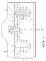
- FIG. 1shows a partial cross-sectional view of a semiconductor device 10 having one or more isolation trench structures 322 in accordance with a first embodiment of the present invention. It is understood that isolation trench structures 322 comprise a plurality of individual trench structures, cells, stripes, or one continuous trench matrix.
- Device 10includes a body or region of semiconductor material 110 , which comprises for example, a p-type silicon substrate 121 , and a semiconductor layer or well region 124 that comprises n-type conductivity.
- semiconductor layer 124is formed using conventional epitaxial growth techniques.
- well region 124is formed using conventional doping and diffusion techniques.
- semiconductor material 110includes a buried layer between substrate 121 and semiconductor layer 124 .
- trench structure 322comprises a trench 422 extending from major surface 18 of semiconductor material 110 .
- trench 422extends through semiconductor layer 124 and reaches substrate 121 .
- trench 422extends partially into semiconductor layer 124 .
- a dielectric layer (or layers) 128is formed overlying lower sidewall and lower surfaces of trench 422 while leaving upper sidewall surfaces of trench 422 exposed or uncovered.
- dielectric layers 128comprise an oxide, a nitride, combinations of the two, or the like.
- dielectric layer 128comprises about 0.15 microns to about 0.25 microns of silicon dioxide.
- a silicon nitride layerabout 0.05 microns to about 0.1 microns is formed overlying the silicon dioxide layer.
- isolation trench structure 322further includes a plug, conformal plug, single crystalline sealing structure, substantially homogeneous plug or epitaxial cap structure or layer 91 .
- plug 91comprises an epitaxially grown single crystalline semiconductor structure extending from upper exposed sidewall portions 423 of trench 422 .
- exposedit is meant that layers 128 are absent from sidewall portions 423 , which exposes portions of semiconductor material 110 / 124 to provide a substantially single crystalline interface in which to grow single crystal epitaxial material.
- plug 91comprises p-type conductivity when semiconductor layer 124 comprises n-type conductivity. That is, the conductivity type of plug 91 is opposite to that of semiconductor layer 124 .
- Plug 91has a dopant concentration sufficient to provide isolation between regions 1001 and 1002 of device 10 .
- plug 91has a dopant concentration in range from about 1.0 ⁇ 10 17 atoms/cm 3 to about 1.0 ⁇ 10 19 atoms/cm 3 .
- plug 91completely seals trench 422 to provide a sealed core or centrally located void region 29 . That is, core 29 is absent solid material. In one embodiment, core 29 comprises a sealed volume containing a gas such as hydrogen. In one embodiment, core 29 is under a vacuum of less than about 20 Torr with 5 to 10 Torr being typical. In another embodiment, plug 91 partially seals trench structure 322 leaving a substantially centrally located gap in plug 91 . In one embodiment, selective epitaxial growth techniques are used to form plug 91 , which leaves exposed major surfaces 129 of dielectric layers 128 substantially absent semiconductor material (i.e., plug 91 does not overlie major surfaces 129 ), which among other things simplifies processing and reduces stress.
- plug 91is planarized so that its upper surface 191 is at about the same level or in proximity to major surface 18 . This is not required, but is useful in space sensitive applications.
- Plugs 91provide, among other things, a reduced stress sealing configuration that also reduces contaminant incorporation within trench 422 .
- plug 91can be configured to provide a complete seal, it is not necessary to completely fill core region 29 with stress-inducing materials such polysilicon or the like.
- plug 91can be configured to provide a complete seal overlying trench 422 , contaminants are not incorporated into the core region of the trench during subsequent processing.
- Device 10further includes optional isolation regions 17 that are, for example, doped p-type (i.e., opposite to the conductivity type of semiconductor layer 124 ) to provide additional isolation.
- plugs 91may be doped or undoped. Isolation regions 17 are formed before or after plugs 91 are formed using conventional techniques.
- Device 10is further shown with a dielectric layer 148 formed overlying or adjacent to major surface 18 .
- dielectric layer 148comprises an oxide, a nitride, combinations of the two, or the like.
- isolation trench structure 322provides isolation between regions 1001 and 1002 .
- isolation trench structure 322provides an isolated region 1003 for forming a component 424 such as passive component.
- component 424is a capacitor, an inductor, an input/output pad or any structure where isolation from semiconductor material 110 or a portion thereof is desired.
- FIG. 2shows a partial cross-sectional view of device 10 at an early step in fabrication.
- isolation regions 17are formed using, for example, conventional masking and doping techniques. As stated previously, isolation regions 17 are optional and may be omitted.
- a dielectric layer 40is formed overlying major surface 18 , and comprises for example, a thermal oxide about 0.03 microns thick.
- a dielectric layer 44 comprising a different material than dielectric layer 40is then formed overlying dielectric layer 40 .
- dielectric layer 44is a silicon nitride when first dielectric layer 40 is a silicon oxide.
- dielectric layer 44is approximately 0.2 microns of silicon nitride, and is formed using conventional deposition techniques.
- a dielectric layer 46is formed overlying dielectric layer 44 and comprises approximately 0.6 microns of deposited silicon dioxide. These layers provide a hard mask structure 112 for subsequent processing. Opening 172 is then formed using conventional techniques to remove portions of layers 46 , 44 , and 40 to expose a portion of major surface 18 .
- trench 422is formed through opening 172 extending from major surface 18 into semiconductor layer 124 .
- trench 422extends into at least a portion of substrate 121 .
- the depth of trench 422is determined by the thickness of semiconductor layer 124 .
- DRIEDeep Reactive Ion Etching
- trench 422has substantially vertical sidewalls.
- trench 422has a tapered profile where the width of the trench at the trench lower surface is less than the width in proximity to major surface 18 .
- trench 422has an expanded profile where the width of the trench at the lower surface is greater than the width of the trench in proximity to major surface 18 .
- the depth of trench 422is in a range from about 3.0 microns to about 100 microns.
- a short selective etchis typically used that may undercut dielectric layer 40 as shown in FIG. 2 .
- a polysilicon layer 47is formed overlying major surface 18 including sidewall and lower surfaces of trench 422 and filling the undercut regions of dielectric layer 40 .
- FIG. 3shows an enlarged partial cross-sectional view of device 10 at a further stage of fabrication.
- a first dielectric layer 28is formed overlying major surface 18 including sidewall and lower surfaces of trench 422 .
- first dielectric layer 28comprises an oxide.
- 0.04 microns of dry oxideis formed consuming polysilicon layer 47 but retaining that portion of polysilicon layer 47 in the undercut regions of layer 40 , followed by about 0.2 microns of deposited oxide.
- a second dielectric layeris formed overlying first dielectric layer 28 .
- the second dielectric layercomprises about 0.1 microns of silicon nitride. Conventional deposition techniques are used to form the first and second dielectric layers.
- dielectric layers 28 and 62may be etched off the lower surface of trench 422 or left in place as shown in FIG. 3 .
- conventional masking stepsmay be used to prevent dielectric layers 28 and 62 from being removed at the lower surface of trench 422 .
- dielectric layer 28is exposed to an additional selective etching step to remove an upper portion of the dielectric material so that dielectric layer 28 is recessed from upper surfaces of dielectric layer 62 . If the lower portions of dielectric layers 28 and 62 were removed in the step described in conjunction with FIG. 2 , the selective etch would also remove dielectric layer 28 from the open area exposed at the bottom of trench 422 .
- dielectric layer 28comprises an oxide
- an isotropic etchsuch as a diluted HF wet etch (e.g., 10:1 for about 8-11 minutes) is used to recess dielectric layer 28 approximately 1.2 microns below dielectric layer 62 .
- dielectric layer 46also may be removed.
- Dielectric layers 62 and 44are then removed using conventional material removal techniques as shown in FIG. 5 to provide exposed portions 423 of semiconductor material 110 at upper portions of trench 422 . This process provides a very controllable way to form exposed portions 423 compared to processes that rely on anisotropic etching.
- FIG. 6shows an enlarged partial cross-sectional view of device 10 after additional processing.
- an epitaxial plug, single crystalline plug, plug of semiconductor material, or homogeneous semiconductor plug region 91is formed within the opening of trench 422 above dielectric layer 28 and along exposed portions 423 of semiconductor layer 124 .
- plug 91comprises an epitaxial semiconductor material that has an opposite conductivity type to semiconductor layer 124 .
- plug 91is p-type.
- plug 91has a dopant concentration between about 1.0 ⁇ 10 17 atoms/cm 3 and about 1.0 ⁇ 10 19 atoms/cm 3 .
- plug 91is undoped.
- a dichlorosilane source gasis used with hydrogen and HCl, which makes the growth selective to exposed portions 423 only.
- silane, disilane, or trichlorosilane source gasesare used.
- epitaxial reactor pressureis set within a range from approximately ten Torr to atmospheric.
- a single wafer reactoris used with a reactor pressure of about 20 Torr during the growth process.
- Suitable growth temperatures for dichlorosilaneare in a range from about 950 degrees Celsius to about 1050 degrees Celsius.
- Suitable growth temperatures for silane or disilaneare in range from about 575 degrees Celsius to about 700 degrees Celsius.
- Suitable growth temperatures for trichlorosilaneare in a range from about 1000 degrees Celsius to about 1200 degrees Celsius.
- plug 91has a thickness in a range from about 0.10 microns to about 0.60 microns. It is understood that the thickness of plug 91 is adjusted according to the width of trench 422 . By way of example, thickness is adjusted depending on the desired structure of plug 91 (e.g., near-closure, complete closure, or overgrowth).
- a growth rate of about 0.30 microns per minuteis used when a selective epitaxial growth technique and dichlorosilane are used.
- a growth rate in a range of about 1.0 micron per minute to about 2.0 microns per minuteis used.
- Gas flow ratesdepend on reactor configuration, and are set by the growth conditions and structure required. In one embodiment, the following gas flows ranges were used in a selective growth process to form plug 91 in a closed configuration using dichlorosilane: 30-40 standard liters per minute (slm) of hydrogen, 0.70-0.80 slm HCl, and 0.20-0.25 slm dichlorosilane.
- plug 91is configured to seal off trench 422 to form sealed core 29 , and is further configured to do so with minimal defects and negligible stress compared to structures that use dielectric/polysilicon or polysilicon fill techniques. By suppressing defects and stress, the reliability and quality of device 10 is improved.
- major surfaces 129 of dielectric layers 28are substantially absent semiconductor material (i.e., plug 91 does not overlie major surfaces 129 ), which among other things simplifies processing and reduces stress. Also, this reduces issues associated with thermally generated carriers. Additionally, this eliminates any parasitic MOS transistor characteristics particularly when plug 91 is doped.
- sealed core 29is under a vacuum of about 20 Torr with some hydrogen present in sealed core 29 from the epitaxial growth process.
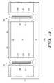
- FIG. 7shows a partial cross-sectional view of an insulated gate field effect transistor (IGFET), MOSFET, superjunction device, superjunction structure, charge-compensated or switching device or cell 100 in accordance with a second embodiment of the present invention.
- IGFETinsulated gate field effect transistor
- MOSFETMOSFET
- superjunction devicesuperjunction structure
- charge-compensated or switching device or cell 100in accordance with a second embodiment of the present invention.
- device 100is among many such devices integrated with logic and/or other components into a semiconductor chip as part of a power integrated circuit.
- device 100is among many such devices integrated together to form a discrete transistor device.
- Device 100includes a region of semiconductor material 11 , which comprises for example, an n-type silicon substrate 12 having a resistivity in range of approximately 0.001 to about 0.01 ohm-cm, and may be doped with arsenic or phosphorous.
- substrate 12provides a drain region for device 100 , which is adjacent to conductive layer 13 .
- a semiconductor layer 14is formed in or on substrate 12 and is n-type or p-type and doped light enough so as to not impact charge balance in the trench compensation regions described below. In one embodiment, layer 14 is formed using conventional epitaxial growth techniques.
- layer 14is doped n-type or p-type with a dopant concentration of about 1.0 ⁇ 10 13 atoms/cm 3 to about 1.0 ⁇ 10 14 atoms/cm 3 , and has a thickness on the order of about 40 microns to about 60 microns. Note that although semiconductor layer 14 is shown as thicker than substrate 12 in the drawings, in reality substrate 12 is thicker. It is shown this way for ease of understanding in the drawings.
- a portion of layer 14is doped p-type in the active region portion of device 100 , while another portion of layer 14 is doped n-type in the edge termination portion of the device.
- the thickness of layer 14is increased or decreased depending on the desired BVdss rating of device 100 .
- semiconductor layer 14comprises a graded dopant profile with semiconductor layer 14 having a higher dopant concentration in proximity to substrate 12 , and transitioning either gradually or abruptly to a lower concentration for the balance of its thickness towards major surface 18 .
- IGBTinsulated gate bipolar transistor
- Device 100further includes spaced apart filled trenches, compensating trenches, semiconductor material filled trenches, charge-compensated trench regions, deep trench charge compensation regions, charge-compensated filled trenches, compensation trenches, localized vertical charge compensation structures, or localized charge compensation regions 22 .
- charge compensationgenerally means that the total charge of the opposite conductivity type layers is substantially or generally balanced or equal.
- Charge-compensated filled trenches 22include a plurality of layers or multiple layers of semiconductor material 220 , including at least two layers of opposite conductivity type (i.e., at least one each of n-type and p-type), which may be separated by an intrinsic, buffer, or lightly doped semiconductor layer or layers. As shown in FIG. 7 , material 220 includes a layer 221 of n-type semiconductor material adjoining semiconductor layer 14 along sidewall surfaces of the trenches.
- layers 221are of the same conductivity type as source regions 33 , and form a primary vertical low resistance current path from the channel to the drain when device 100 is in the on-state.
- a layer 222 of compensating p-type semiconductor materialis formed overlying layer 221 .
- n-type layers 221 and p-type layers 222have a dopant concentration on the order of about 9.0 ⁇ 10 15 to about 5.0 ⁇ 10 16 atoms/cm 3 , and each has a thickness of about 0.1 microns to about 0.3 microns respectively.
- p-type layers 222 and n-type layers 221compensate each other to provide an increased BVdss characteristic.
- layers of semiconductor material 220comprise a single crystalline semiconductor material. Additional details regarding charge-compensated trenches 22 and layers of semiconductor material 220 are described below in conjunction with FIGS. 4 and 5 .
- device 100includes a dielectric layer 28 formed overlying portions of layers of semiconductor material 220 .
- dielectric layer 28is formed overlying a portion of sidewall surfaces and lower surfaces of layers of semiconductor material 220 while leaving upper sidewall portions exposed. This is shown for example in FIG. 7 .
- dielectric layer 28is a deposited silicon oxide layer having a thickness of about 0.2 microns.
- charge-compensated trenches 22are configured or formed with a void or sealed core 29 at a centrally located portion and are capped with a plug structure 91 .
- plugs 91comprise a single crystal semiconductor material, which is epitaxially grown along upper portions of layers of semiconductor material 220 to seal off charge-compensated trenches 22 .
- the single crystal semiconductor materialis subsequently planarized so that upper surfaces of plugs 91 are in proximity to major surface 18 .
- charge-compensated trenches 22are voidless, and filled with materials such as dielectrics, polycrystalline semiconductor material, single crystal semiconductor material, or combinations thereof.
- n-type dopant from highly doped substrate 12diffuses into the lower portions of charge-compensated trenches 22 so that those portions of trenches 22 within substrate 12 become more heavily doped n-type.
- Device 100also includes a well, base, body or doped regions 31 formed in semiconductor layer 14 between and in proximity to, adjacent to, or adjoining charge-compensated trenches 22 .
- Body regions 31extend from major surface 18 of semiconductor material 11 .
- body regions 31comprise p-type conductivity, and have a dopant concentration suitable for forming an inversion layer that operates as conduction channels 45 of device 100 .
- Body regions 31extend from major surface 18 to a depth of about 1.0 to about 5.0 microns.
- body regions 31comprise a plurality of individually diffused regions or comprise a connected, single or commonly diffused region of selected shape.
- N-type source regions 33are formed within, above, or in body regions 31 and extend from major surface 18 to a depth of about 0.2 microns to about 0.5 microns. In the embodiment shown, portions of major surface 18 extend down and then outward from the edges of source regions 33 so that contact is made to horizontal and vertical surfaces of source regions 33 by source contact layer 63 .
- One or more p-type body contact regions 36are formed in at least a portion of each body region 31 . Body contact regions 36 are configured to provide a lower contact resistance to body region 31 , and to lower the sheet resistance of body regions 31 under source regions 33 , which suppresses parasitic bipolar transistor effects.
- body contact regions 36 and body regions 31overlie charge-compensated trenches 22 as shown in FIG. 7 , and together with source contact layer 63 are configured to provide ohmic contact to and continuity with p-type layers 222 in charge-compensated trenches 22 .
- This ohmic contact structureis configured to provide a grounded structure for p-type layers 222 , which eliminates lateral electric fields at major surface 18 and improves the breakdown voltage performance of device 100 .
- This structurealso grounds the effects of any defects present in proximity to major surface 18 and within or in proximity to charge-compensated trenches 22 .
- the structure of device 100greatly simplifies the ability to make contact to layers 222 , which is necessary for optimum device performance. In particular, device 100 avoids using any complex topography overlying the upper portion of charge-compensated trenches 22 , which simplifies the ohmic contact structure and method.
- Device 100further includes a trench gate or control structure 157 adjoining body regions 31 and source regions 33 .
- Control structure 157is laterally spaced apart from adjacent charge-compensated trenches 22 . That is, control structure 157 does not overlie charge-compensated trenches 22 .
- Trench gate structure 157includes a gate trench 158 and a gate dielectric layer 43 formed overlying surfaces of gate trench 158 .
- gate dielectric layer 43comprises a silicon oxide, and has a thickness of about 0.05 microns to about 0.1 microns.
- gate dielectric layer 43has a thickness at the lower surfaces of gate trench 158 that is greater or thicker than the thickness of gate dielectric layer 43 along the sidewalls of gate trench 158 .
- gate dielectric layer 43comprises silicon nitride, tantalum pentoxide, titanium dioxide, barium strontium titanate, or combinations thereof including combinations with silicon oxide, or the like.
- Trench gate structure 157further includes a conductive gate region 57 formed within control or gate trench 158 and overlies gate dielectric layer 43 .
- a source region 33is interposed between a conductive gate region 57 and a charge compensation trench 22 .
- Conductive gate region 57comprises, for example, n-type polysilicon. Although conductive gate region 57 is shown as recessed below major surface 18 , conductive gate region 57 may extend higher or above major surface 18 .
- Trench gate structure 157is configured to control the formation of channels 45 and the conduction of current in device 100 .
- device 100further includes n-type doped layers or sub-surface doped layers 26 .
- doped layers 26are configured to provide a sub-surface conduction path between the drain end of channels 45 and n-type layers 221 , which are the primary conduction layers or vertical conduction paths in charge compensation trenches 22 . That is, in device 100 current flows vertically through channels 45 , then horizontally through doped layers 26 , and then vertically through layers 221 .
- Doped layers 26are configured so that current flow is isolated from major surface 18 by body regions 31 and body contact regions 36 , which are opposite conductivity types (p-type) from doped layers 26 (n-type).
- This isolation featurekeeps the conduction path away from defect regions near the surface thereby avoiding any conduction related problems.
- the grounded p-type layer 222 structurefurther isolates the effects of any high defect density regions from the primary conduction path.
- a preferred concave-shaped junctionis provided, which surrounds n-type layers 221 and doped layer 26 . This beneficially enhances BVdss.
- Device 100further includes an interlayer dielectric region 48 formed overlying major surface 18 , which is patterned to provide openings to body contact regions 36 and source regions 33 .
- a portion of interlayer dielectric region 48is left overlying trench gate structure 57 to provide isolation for conductive gate region 57 .
- Interlayer dielectric region 48comprises for example, a silicon oxide such as a deposited oxide, and has a thickness from about 0.4 microns to about 1.0 microns.
- Source contact layer 63is formed overlying major surface 18 and makes contact to both source regions 33 and body contact regions 36 .
- source contact layer 63comprises a titanium/titanium nitride barrier layer and an aluminum silicon alloy formed overlying the barrier layer, or the like.
- Drain contact layer 13is formed overlying an opposing surface of semiconductor material 11 , and comprises, for example, a solderable metal structure such as titanium-nickel-silver, chrome-nickel-gold, or the like. In the alternative, layer 13 comprises a conductive epoxy or the like.
- the structure and method of device 100places primary conduction layer 221 adjacent the sidewall surface of charge-compensated trenches 22 .
- Device 100uses a trench gate control structure 157 , which places the drain end of channel 45 spaced apart, away, or sub-surface from major surface 18 .
- Device 100incorporates sub-surface doped layers 26 that electrically connect the sub-surface drain ends of channels 45 to primary conduction layers 221 in charge-compensated trenches 22 .
- This approachmoves the primary current path away from the surface of the device, which makes it much less susceptible to stress issues and defects thereby improving performance.
- the primary current path of device 100is configured this way, forming the ohmic contact structure between p-type compensating doped layers 222 , body regions 31 , body contact regions 36 and source contact layer 63 is simplified.
- I Dflows vertically through n-type layers 221 to produce a low on resistance, and horizontally through sub-surface doped layers 26 keeping the current path isolated from major surface 18 .
- I D1.0 amperes.
- V Ga control voltage of less than the conduction threshold of the device is applied to conductive gate regions 157 (e.g., V G ⁇ 5.0 volts). This removes channels 45 and I D no longer flows through device 100 .
- n-type layers 221 and p-type layers 222compensate each other as the depletion region from the primary blocking junction spreads, which enhances BVdss.
- device 100Another advantage of device 100 is that the simplified ohmic contact structure between p-type compensating doped layers 222 , body region 31 , body contact region 36 and source contact layer 63 enhances switching characteristics. For example, when device 100 switches from an on state to an off state, the ohmic contact pulls both electrons and holes from the structure more efficiently.
- FIG. 8shows an enlarged partial cross-sectional view of device 100 at an early stage of fabrication.
- a dielectric layer 40is formed overlying major surface 18 , and comprises for example, a thermal oxide about 0.2 microns thick.
- a dielectric layer 44comprising a different material than dielectric layer 40 is then formed overlying dielectric layer 40 .
- dielectric layer 44is a silicon nitride when first dielectric layer 40 is a silicon oxide.
- dielectric layer 44is approximately 0.2 microns of silicon nitride, and is formed using conventional deposition techniques.
- a dielectric layer 46is formed overlying dielectric layer 44 and comprises approximately 0.6 microns of deposited silicon dioxide. These layers provide an example of a hard mask structure 112 for subsequent processing.
- FIG. 9shows an enlarged partial cross-sectional view of device 100 at a subsequent stage of fabrication.
- Hard mask structure 112is patterned using conventional photolithographic and material removal techniques to form openings 72 , which expose portions of major surface 18 .
- openings 72have a width 74 of about 3.0 microns to about 4.0 microns.
- trenches 122are formed through openings 72 extending from major surface 18 into semiconductor layer 14 .
- semiconductor layer 14has a width 75 between adjacent trenches 122 of about 2.0 microns to 3.0 microns. To ease the understanding of this embodiment, width 75 is shown greater than width 74 with the understanding that width 75 may be less than or equal width 74 .
- trenches 122extend into at least a portion of substrate 12 . The depth of trenches 122 is determined by the thickness of semiconductor layer 14 , which is a function of BVdss requirements.
- DRIEDeep Reactive Ion Etching
- trenches 122have substantially vertical sidewalls.
- trenches 122have a tapered profile where the width of the trench at the trench lower surface is less than width 74 .
- trenches 122are stated as plural, it is understood that trenches 122 may be a single continuous trench or connected trench matrix. Alternatively, trenches 122 may be a plurality of individual trenches with closed ends and separated by portions of body of semiconductor material 11 . The depth of trenches 122 is in a range from about 3.0 microns to about 100 microns.
- FIG. 10shows an enlarged partial cross-sectional view of device 100 at a later stage of fabrication.
- layers of semiconductor material 220are formed, grown, or deposited in trenches 122 as a first step in forming charge-compensated trenches 22 .
- single crystal semiconductor epitaxial growth techniquesare used to form layers of semiconductor material 220 .
- a thin oxidesuch as a thermal oxide (not shown) is formed on the sidewalls of trenches 122 to remove any surface damage caused by the material removal step.
- the thin oxideis then removed using conventional isotropic etching techniques (e.g., 10:1 wet oxide strip).
- semiconductor material 11is placed into an epitaxial growth reactor and pre-cleaned as a first step in the epitaxial growth process.
- silicon source gasessuch as trichlorosilane (SiHCl 3 ), dichlorosilane (SiH 2 Cl 2 ), silane (SiH 4 ) or disilane (Si 2 H 6 ) are suitable for forming these layers.
- FIG. 11is a partial cross-sectional view of a portion 1011 of trench 122 in FIG. 10 .
- all layers that make up layers of semiconductor material 220are grown in continuous manner inside the epitaxial reactor.
- the epitaxial growth conditionsare set to provide a mean free path roughly equal to or greater than the depth of trenches 122 .
- the aspect ratio of trenches 122be in a range from about 1:1 to about 30:1 to provide good quality epitaxial layers.
- a selective epitaxial growth processis used to avoid growing epitaxial silicon overlying dielectric layer 46 , which would produce polycrystalline silicon.
- Selectivityis controlled by adding HCl gas to the epitaxial growth chamber in an amount sufficient to suppress growth of silicon on the dielectric layers.
- the HCl flow rateis set to be in a range from greater than zero to about four to five times the flow rate of the silicon source gas.
- blanket layersare grown (i.e., the layers are grown overlying major surface 18 in addition to trenches 122 ), and planarization techniques are used to remove portions of the blanket layers that overlie major surface 18 .
- an intrinsic layer 21is formed first along the surfaces of trenches 122 , and has a thickness of about 0.05 to about 0.1 microns. Intrinsic layer 21 preferably is undoped, and functions, among other things, to smooth out any irregularities on the sidewall and lower surfaces of trenches 122 .
- N-type layer 23is then formed overlying layer 21 , with a phosphorous, arsenic or antimony dopant source being suitable.
- n-type layer 23is lightly doped and has a dopant concentration on the order of about 1.0 ⁇ 10 15 to about 1.0 ⁇ 10 17 atoms/cm 3 .
- N-type layer 23has a thickness typically less than about 1.0 microns, with a thickness of about 0.1 microns to about 0.4 microns being one preferred range.
- an intrinsic layer 24is formed overlying n-type layer 23 , and has thickness of about 0.1 to about 0.4 microns.
- intrinsic layer 24is undoped.
- a p-type layer 25is then formed overlying second intrinsic layer 24 , with boron being a suitable dopant source.
- p-type layer 25has a dopant concentration on the order of about 1.0 ⁇ 10 15 to about 1.0 ⁇ 10 17 atoms/cm 3 .
- P-type layer 25has a thickness typically less than about 1.0 microns, with a thickness of about 0.1 microns to about 0.3 microns being one preferred range.
- One purpose of intrinsic layer 24is to improve conduction by reducing the mutual depletion of layers 23 and 25 at low drain voltage, which provides higher conduction efficiency.
- an intrinsic layer 27is formed overlying p-type layer 25 , and has a thickness of about 0.1 to about 1.0 microns.
- n-type dopant in n-type layer 23diffuses into intrinsic layers 21 and 24 to form n-type layer 221 as shown in FIGS. 7 and 10
- p-type layer 25diffuses into intrinsic layers 24 and 27 to form p-type layer 222 as shown in FIGS. 7 and 10 .
- the multiple layers shown in FIG. 11are not shown in the other figures for ease of understanding.
- the dopant concentrations and thicknesses of n-type layers 221 and p-type layers 222are configured to provide an appropriately balanced charge when device 100 is in operation.
- the center or central portion of trenches 122is left open (i.e., that portion is not completely filled with a solid material).
- the epitaxial reactoris purged of HCl, source, and dopant gases, and device 100 is exposed to hydrogen at an elevated temperature. This smoothes out the topography of the outer surfaces of layers of semiconductor materials 220 , which, among other things, enhances subsequent processing including the formation of plugs 91 .
- FIG. 12shows an enlarged partial cross-sectional view of device 100 at a still further stage of fabrication.
- a first dielectric layeris formed overlying major surface 18 and layers of semiconductor material 220 in trenches 122 .
- this first dielectric layercomprises an oxide.
- 0.02 microns of dry oxideare formed, followed by about 0.2 microns of deposited oxide.
- a second dielectric layeris formed overlying the first dielectric layer.
- the second dielectric layercomprises about 0.1 microns of silicon nitride. Conventional deposition techniques are used to form the first and second dielectric layers.
- layer 28comprises about 0.02 microns of dry oxide and about 0.2 microns of deposited oxide and layer 62 comprises about 0.1 microns of silicon nitride.
- dielectric layer 28is exposed to an additional selective etching step to remove an upper portion of the dielectric material so that dielectric layer 28 is recessed from upper surfaces of dielectric layer 62 .
- a diluted HF wet etche.g., 10:1 for about 8-11 minutes
- dielectric layer 46also may be removed. Dielectric layers 62 and 44 are then removed using conventional material removal techniques as shown in FIG. 14 .
- FIG. 15shows an enlarged partial cross-sectional view of device 100 after additional processing.
- an epitaxial plug, single crystalline plug, plug of semiconductor material, or semiconductor plug region 91is formed within the remaining openings of trenches 122 above dielectric layers 28 and along exposed portions of layers of semiconductor material 220 .
- plugs 91comprise an epitaxial semiconductor material that has an opposite conductivity type to semiconductor layer 14 .
- plugs 91are p-type.
- plugs 91have a dopant concentration between about 1.0 ⁇ 10 17 atoms/cm 3 and about 1.0 ⁇ 10 19 atoms/cm 3 .
- plugs 91are undoped.
- reduced pressure and selective epitaxial growth techniquesare used to form plugs 91 .
- a dichlorosilane source gasis used with hydrogen and HCl, which makes the growth selective to the upper portions of trenches 122 only.
- silane, disilane, or trichlorosilane source gasesare used.
- reactor pressureis set within a range from approximately ten Torr to atmospheric.
- a single wafer reactoris used with a reactor pressure of about 20 Torr.
- Suitable growth temperatures for dichlorosilaneare in a range from about 950 degrees Celsius to about 1050 degrees Celsius.
- Suitable growth temperatures for silane or disilaneare in range from about 575 degrees Celsius to about 700 degrees Celsius.
- Suitable growth temperatures for trichlorosilaneare in a range from about 1050 degrees Celsius to about 1175 degrees Celsius. Caution is required with higher growth temperatures to avoid unwanted intermixing of dopants within the various epitaxial layers or doped regions of device 100 .
- plugs 91have thicknesses in the range of about 0.10 microns to about 0.60 microns. By way of example, thickness is adjusted depending on the desired structure of plugs 91 (e.g., near-closure, complete closure, or overgrowth).
- a growth rate of about 0.30 microns per minuteis used when selective epitaxial growth techniques and dichlorosilane are used.
- a growth rate in a range of about 1.0 micron to about 2.0 micronsis used.
- Gas flow ratesdepend on reactor configuration, and are set by the growth conditions and structure required. In one embodiment, the following gas flows ranges were used in a selective growth process to form plugs 91 in a closed configuration using dichlorosilane: 30-40 standard liters per minute (slm) of hydrogen, 0.70-0.80 slm HCl, and 0.20-0.25 slm dichlorosilane.
- plugs 91are configured to seal off voids 29 in trenches 122 , and are further configured to do so with minimal defects and negligible stress compared to structures that use dielectric/polysilicon or polysilicon fill techniques. By suppressing defects and stress, the reliability and quality of device 100 is improved.
- sealed cores 29are under a vacuum of less than about 20 Torr with some hydrogen present in sealed cores 29 from the epitaxial growth process.
- a polycrystalline semiconductor layer 92is formed overlying major surface 18 .
- layer 92comprises a polysilicon layer about 0.6 microns to about 0.9 microns thick and is formed using conventional deposition techniques.
- a planarizing photoresist layer 93 on the order of 1.0 to 2.0 micronsis then formed overlying polycrystalline semiconductor layer 92 .
- FIG. 16is an enlarged partial cross-sectional view of device 100 after a planarizing or bulk removal process is used to remove layer 93 , layer 92 , and exposed or upper portions of plugs 91 .
- a planarizing or bulk removal processis used to remove layer 93 , layer 92 , and exposed or upper portions of plugs 91 .
- conventional etch back techniquesare used for this removal step.
- chemical mechanical planarization techniquesare used.
- Layer 40(shown in FIG. 15 ) is then removed using, for example, a wet chemical etch.
- a dielectric layer 94is formed overlying major surface 18 and comprises, for example, an implant oxide having a thickness of about 0.05 microns to about 0.09 microns.
- a patterned photoresist layer 96is then formed overlying major surface 18 in preparation for forming doped layers 26 .
- Dopant for doped layers 26is then introduced or provided into semiconductor layer 14 below major surface 18 using patterned photoresist layer 96 as a mask.
- high energy ion implantationis used to implant dopant for doped layers 26 .
- a MeV range implant of phosphorousis used, and an implant dose of about 1.0 ⁇ 10 12 atoms/cm 2 is sufficient.
- the dopant concentration of layer 26is greater than the dopant concentration of semiconductor layer 14 to provide a path having reduced resistance between channels 45 (shown in FIG. 1 ) and n-type layers 221 .
- the high energy implantplaces doped layer 26 below major surface 18 as shown in FIG. 16 so that doped layer 26 is sub-surface.
- Patterned photoresist layer 96is then removed.
- the implanted dopantis then heat treated to diffuse the n-type dopant into semiconductor layer 14 to a selected depth.
- doped layer 26extends to a depth of about 2.0 microns to about 3.0 microns.
- body region 31shown in FIG. 17 .
- a combined heat treatment stepis used after dopant for body regions 31 is introduced as described below in FIG. 17 .
- doped layers 26are formed prior to the formation of trenches 122 .
- doped layers 26are formed prior to the formation of hard mask 112 shown in FIG. 8 .
- FIG. 17shows an enlarged partial cross-sectional view of device 100 at a later step of fabrication.
- P-type dopant for body regions 31is introduced or provided at major surface 18 .
- body regions 31extend laterally to overlie all or portions of compensation trenches 22 . That is, body regions 31 overlap at least p-type layers 222 .
- ion implantationis used with a boron implant dose of about 1.0 ⁇ 10 13 atoms/cm 2 and an implant energy of about 160 KeV.
- a series of boron implantsare used to form body region 31 , with a lighter dose/higher energy implant occurring first followed by gradually increasing doses and gradually decreasing energy implants occurring thereafter.
- implanted p-type dopantis heat treated to diffuse and/or activate the dopant to form regions 31 .
- body regions 31have a depth of about 1.0 to about 2.0 microns.
- FIG. 18is an enlarged partial cross-sectional view of device 100 after completing preliminary steps in the formation of a control or gate trench 158 .
- a dielectric layer 98is formed overlying dielectric layer 94 .
- dielectric layer 98comprises a silicon nitride layer about 0.1 microns to about 0.2 microns thick and is formed using conventional techniques.
- a layer of photoresist(not shown) is deposited overlying dielectric layer 98 and an opening is formed for control trench 158 . Portions of layers 98 and 94 are then removed to expose a portion of major surface 18 . The photoresist layer is then removed.
- control trench 158is formed extending from major surface 18 generally centrally located between adjacent charge-compensated trenches 22 .
- a conventional anisotropic dry etchis used to form control trench 158 .
- control trench 158has a width of about 0.4 microns to about 0.7 microns and has a depth greater than the depth of body regions 31 .
- control trench 158has a depth greater than doped regions 26 .
- control trench 158has a depth of about 1.0 microns to about 1.6 microns.
- FIG. 19is an enlarged partial cross-sectional view of device 100 after further processing.
- a thin thermal oxideis grown overlying the exposed surfaces of control trench 158 . This oxide is then removed. Dielectric layer 98 also is removed.
- gate dielectric layer 43is formed overlying surfaces of control trench 158 .
- gate dielectric layer 43comprises silicon oxide and has a thickness of about 0.05 microns to about 0.1 microns. In another embodiment, gate dielectric layer 43 is thicker along the bottom portion and lower sidewall portions of control trench 158 .
- a conductive layersuch as a doped or undoped polysilicon layer is then deposited overlying gate dielectric layer 43 and partially removed to form gate conductive region 57 .
- gate conductive regions 57comprise about 0.2 microns of doped or undoped polysilicon. If gate conductive region 57 is initially undoped, this region is subsequently doped during the formation of source regions 33 . In one embodiment, gate conductive region 57 is recessed below major surface 18 . Together, control trench 158 , gate dielectric layer 43 and gate conductive region 57 form control structure 157 . In an alternative embodiment, control structure 157 is formed prior to the formation of charge-compensated trenches 22 . This alternative approach is used when the impact of the thermal budget on the dopant profiles of layers 221 and 222 is a concern. The configuration of doped regions 26 is conveniently flexible enough to support either process sequence.
- Source regions 33are then formed using, for example, a phosphorous or arsenic ion implant and anneal step.
- a phosphorous or arsenic ion implantis used with a dose 1.0 ⁇ 10 15 atoms/cm 2 to about 5.0 ⁇ 10 15 atoms/cm 2 being sufficient.
- This dopantis activated using, for example, a rapid anneal of 45 seconds at 1030 degrees Celsius.
- source regions 33are formed on both sides of control structure 157 .
- interlayer dielectric region 48is formed overlying major surface 18 .
- interlayer dielectric 48comprises a deposited oxide and has a thickness on the order of about 1.0 micron.
- a conventional contact photoresist and etch processis then used to form contact openings 116 overlying and exposing portions of major surface 18 as shown in FIG. 20 .
- an anisotropic etchis then used to remove a portion of semiconductor layer 14 adjacent source regions 33 and above body regions 31 and compensation trenches 22 .
- enough material from semiconductor layer 14is removed to extend to about the depth of source regions 33 or deeper.
- An additional dopantis then added to portions of major surface 18 above body regions 31 and compensation trenches 22 to form body contact regions 36 .
- a boron ion implantis used with an implant dose on the order of 1.0 ⁇ 10 15 atoms/cm 2 to about 5.0 ⁇ 10 15 atoms/cm 2 being sufficient.
- the implanted dopantis then activated using, for example, a rapid anneal process.
- Portions of interlayer dielectric layer 48are then removed along the sides to expose upper surface portions of source regions 33 (shown in FIG. 7 ).
- Source contact layer 63is then formed overlying major surface 18 and makes contact to both source regions 33 and body regions 36 as shown in FIG. 7 .
- source contact layer 63comprises a titanium/titanium nitride barrier layer and an aluminum silicon alloy formed overlying the barrier layer, or the like.
- Drain contact layer 13is formed overlying an opposing surface of semiconductor material 11 as shown in FIG. 7 , and comprises, for example, a solderable metal structure such as titanium-nickel-silver, chrome-nickel-gold, or the like. In an alternative embodiment, layer 13 comprises a conductive epoxy or the like.
- a semiconductor device having a trench structure with a single crystal sealing plughas been described including a method of manufacture.
- the sealing plugprovides, among other things, a reduced stress sealing configuration that also reduces the incorporation of contaminates in the core region of the trench. This provides a more reliable device.
- the trench structurereduces the impacts of parasitic devices in proximity to the trench.
- the trench structure describedis suitable for many applications including but not limited to trench isolation structures and super junction structures.
Landscapes
- Engineering & Computer Science (AREA)
- Physics & Mathematics (AREA)
- Condensed Matter Physics & Semiconductors (AREA)
- General Physics & Mathematics (AREA)
- Manufacturing & Machinery (AREA)
- Computer Hardware Design (AREA)
- Microelectronics & Electronic Packaging (AREA)
- Power Engineering (AREA)
- Element Separation (AREA)
- Insulated Gate Type Field-Effect Transistor (AREA)
Abstract
Description
Claims (7)
Priority Applications (6)
| Application Number | Priority Date | Filing Date | Title |
|---|---|---|---|
| US12/206,541US7902075B2 (en) | 2008-09-08 | 2008-09-08 | Semiconductor trench structure having a sealing plug and method |
| TW098121052ATWI482236B (en) | 2008-09-08 | 2009-06-23 | Semiconductor trench structure and method with sealed plug |
| CN2009101402400ACN101673737B (en) | 2008-09-08 | 2009-07-09 | Semiconductor trench structure having a sealing plug and method |
| KR1020090081345AKR101632938B1 (en) | 2008-09-08 | 2009-08-31 | Semiconductor trench structure having a sealing plug and method |
| HK10107005.6AHK1141135B (en) | 2008-09-08 | 2010-07-20 | Semiconductor trench structure having a sealing plug and method |
| US13/005,947US8106436B2 (en) | 2008-09-08 | 2011-01-13 | Semiconductor trench structure having a sealing plug |
Applications Claiming Priority (1)
| Application Number | Priority Date | Filing Date | Title |
|---|---|---|---|
| US12/206,541US7902075B2 (en) | 2008-09-08 | 2008-09-08 | Semiconductor trench structure having a sealing plug and method |
Related Child Applications (1)
| Application Number | Title | Priority Date | Filing Date |
|---|---|---|---|
| US13/005,947DivisionUS8106436B2 (en) | 2008-09-08 | 2011-01-13 | Semiconductor trench structure having a sealing plug |
Publications (2)
| Publication Number | Publication Date |
|---|---|
| US20100059815A1 US20100059815A1 (en) | 2010-03-11 |
| US7902075B2true US7902075B2 (en) | 2011-03-08 |
Family
ID=41798473
Family Applications (2)
| Application Number | Title | Priority Date | Filing Date |
|---|---|---|---|
| US12/206,541Active2029-06-23US7902075B2 (en) | 2008-09-08 | 2008-09-08 | Semiconductor trench structure having a sealing plug and method |
| US13/005,947ActiveUS8106436B2 (en) | 2008-09-08 | 2011-01-13 | Semiconductor trench structure having a sealing plug |
Family Applications After (1)
| Application Number | Title | Priority Date | Filing Date |
|---|---|---|---|
| US13/005,947ActiveUS8106436B2 (en) | 2008-09-08 | 2011-01-13 | Semiconductor trench structure having a sealing plug |
Country Status (4)
| Country | Link |
|---|---|
| US (2) | US7902075B2 (en) |
| KR (1) | KR101632938B1 (en) |
| CN (1) | CN101673737B (en) |
| TW (1) | TWI482236B (en) |
Cited By (7)
| Publication number | Priority date | Publication date | Assignee | Title |
|---|---|---|---|---|
| US9219138B2 (en) | 2012-10-05 | 2015-12-22 | Semiconductor Components Industries, Llc | Semiconductor device having localized charge balance structure and method |
| US9287371B2 (en) | 2012-10-05 | 2016-03-15 | Semiconductor Components Industries, Llc | Semiconductor device having localized charge balance structure and method |
| US9461063B1 (en) | 2015-05-06 | 2016-10-04 | Macronix International Co., Ltd. | Method for forming a semiconductor structure |
| US9536997B1 (en)* | 2015-09-10 | 2017-01-03 | Kabushiki Kaisha Toshiba | Semiconductor device |
| US9768247B1 (en) | 2016-05-06 | 2017-09-19 | Semiconductor Components Industries, Llc | Semiconductor device having improved superjunction trench structure and method of manufacture |
| US10388774B2 (en)* | 2017-12-04 | 2019-08-20 | Kabushiki Kaisha Toshiba | Semiconductor device |
| US10410861B2 (en)* | 2017-03-07 | 2019-09-10 | Tokyo Electron Limited | Method of filling retrograde recessed features |
Families Citing this family (22)
| Publication number | Priority date | Publication date | Assignee | Title |
|---|---|---|---|---|
| US7679146B2 (en)* | 2006-05-30 | 2010-03-16 | Semiconductor Components Industries, Llc | Semiconductor device having sub-surface trench charge compensation regions |
| JP5423018B2 (en)* | 2009-02-02 | 2014-02-19 | 三菱電機株式会社 | Semiconductor device |
| CN102184860A (en)* | 2011-04-08 | 2011-09-14 | 上海先进半导体制造股份有限公司 | Cold MOS (Metal Oxide Semiconductor) groove padding method and cold MOS groove structure |
| CN102184861A (en)* | 2011-04-08 | 2011-09-14 | 上海先进半导体制造股份有限公司 | Trench filling method and trench structure of cold MOS (metal oxide semiconductor) |
| JP6142496B2 (en)* | 2012-10-12 | 2017-06-07 | 富士電機株式会社 | Manufacturing method of semiconductor device |
| US9112026B2 (en) | 2012-10-17 | 2015-08-18 | Semiconductor Components Industries, Llc | Semiconductor devices and method of making the same |
| JP6054272B2 (en)* | 2013-09-13 | 2016-12-27 | 株式会社東芝 | Semiconductor device |
| US9064699B2 (en) | 2013-09-30 | 2015-06-23 | Samsung Electronics Co., Ltd. | Methods of forming semiconductor patterns including reduced dislocation defects and devices formed using such methods |
| JP2016058546A (en)* | 2014-09-09 | 2016-04-21 | 株式会社東芝 | Semiconductor device |
| KR102318197B1 (en)* | 2014-09-22 | 2021-10-26 | 삼성전자주식회사 | Pixel for CMOS Image Sensor and Image Sensor including the same |
| TWI574386B (en)* | 2015-05-12 | 2017-03-11 | 旺宏電子股份有限公司 | Method for forming a semiconductor structure |
| US20170373142A1 (en)* | 2016-06-23 | 2017-12-28 | Littelfuse, Inc. | Semiconductor device having side-diffused trench plug |
| TWI612661B (en)* | 2017-01-05 | 2018-01-21 | 立錡科技股份有限公司 | Method for improving threshold voltage drop of metal oxide semiconductor device and metal oxide semiconductor device for improving threshold voltage drop |
| WO2019139573A1 (en)* | 2018-01-10 | 2019-07-18 | Intel Corporation | Techniques to reduce substrate coupling for monolithically integrated rf circuits |
| TWI685106B (en)* | 2018-03-09 | 2020-02-11 | 全宇昕科技股份有限公司 | High voltage Schottky diode |
| US10608122B2 (en)* | 2018-03-13 | 2020-03-31 | Semicondutor Components Industries, Llc | Schottky device and method of manufacture |
| US20200098857A1 (en)* | 2018-09-25 | 2020-03-26 | Semiconductor Components Industries, Llc | Narrow-mesa super-junction mosfet |
| KR102828447B1 (en)* | 2019-07-02 | 2025-07-03 | 삼성전자주식회사 | Semiconductor device and manufacturing method thereof |
| CN110767744B (en)* | 2019-10-31 | 2022-03-08 | 上海华虹宏力半导体制造有限公司 | Super junction and manufacturing method thereof |
| JP7249269B2 (en)* | 2019-12-27 | 2023-03-30 | 株式会社東芝 | Semiconductor device and its manufacturing method |
| US20230051830A1 (en)* | 2021-08-13 | 2023-02-16 | Infineon Technologies Ag | Semiconductor device and method of producing thereof |
| US12040252B2 (en)* | 2022-07-06 | 2024-07-16 | Globalfoundries U.S. Inc. | Microfluidic channels sealed with directionally-grown plugs |
Citations (57)
| Publication number | Priority date | Publication date | Assignee | Title |
|---|---|---|---|---|
| US4899199A (en) | 1983-09-30 | 1990-02-06 | International Rectifier Corporation | Schottky diode with titanium or like layer contacting the dielectric layer |
| US5216275A (en) | 1991-03-19 | 1993-06-01 | University Of Electronic Science And Technology Of China | Semiconductor power devices with alternating conductivity type high-voltage breakdown regions |
| US5418185A (en) | 1993-01-21 | 1995-05-23 | Texas Instruments Incorporated | Method of making schottky diode with guard ring |
| US5438215A (en) | 1993-03-25 | 1995-08-01 | Siemens Aktiengesellschaft | Power MOSFET |
| US5571738A (en) | 1992-09-21 | 1996-11-05 | Advanced Micro Devices, Inc. | Method of making poly LDD self-aligned channel transistors |
| US5604159A (en)* | 1994-01-31 | 1997-02-18 | Motorola, Inc. | Method of making a contact structure |
| US5859465A (en) | 1996-10-15 | 1999-01-12 | International Rectifier Corporation | High voltage power schottky with aluminum barrier metal spaced from first diffused ring |
| US5872421A (en) | 1996-12-30 | 1999-02-16 | Advanced Vision Technologies, Inc. | Surface electron display device with electron sink |
| US5886383A (en) | 1997-01-10 | 1999-03-23 | International Rectifier Corporation | Integrated schottky diode and mosgated device |
| US5990011A (en)* | 1997-09-18 | 1999-11-23 | Micron Technology, Inc. | Titanium aluminum alloy wetting layer for improved aluminum filling of damescene trenches |
| US5998288A (en)* | 1998-04-17 | 1999-12-07 | Advanced Micro Devices, Inc. | Ultra thin spacers formed laterally adjacent a gate conductor recessed below the upper surface of a substrate |
| US6078090A (en) | 1997-04-02 | 2000-06-20 | Siliconix Incorporated | Trench-gated Schottky diode with integral clamping diode |
| US6184555B1 (en) | 1996-02-05 | 2001-02-06 | Siemens Aktiengesellschaft | Field effect-controlled semiconductor component |
| US6191446B1 (en) | 1998-03-04 | 2001-02-20 | Advanced Micro Devices, Inc. | Formation and control of a vertically oriented transistor channel length |
| US6210999B1 (en) | 1998-12-04 | 2001-04-03 | Advanced Micro Devices, Inc. | Method and test structure for low-temperature integration of high dielectric constant gate dielectrics into self-aligned semiconductor devices |
| US6255152B1 (en) | 1999-10-01 | 2001-07-03 | United Microelectronics Corp. | Method of fabricating CMOS using Si-B layer to form source/drain extension junction |
| US6274904B1 (en) | 1998-09-02 | 2001-08-14 | Siemens Aktiengesellschaft | Edge structure and drift region for a semiconductor component and production method |
| US6278165B1 (en) | 1998-06-29 | 2001-08-21 | Kabushiki Kaisha Toshiba | MIS transistor having a large driving current and method for producing the same |
| US6291333B1 (en)* | 2000-04-07 | 2001-09-18 | Taiwan Semiconductor Manufacturing Co., Ltd | Method of fabricating dual damascene structure |
| WO2002019433A2 (en) | 2000-08-31 | 2002-03-07 | General Semiconductor, Inc. | Trench schottky rectifier |
| US6355955B1 (en) | 1998-05-14 | 2002-03-12 | Advanced Micro Devices, Inc. | Transistor and a method for forming the transistor with elevated and/or relatively shallow source/drain regions to achieve enhanced gate electrode formation |
| US6410955B1 (en) | 2001-04-19 | 2002-06-25 | Micron Technology, Inc. | Comb-shaped capacitor for use in integrated circuits |
| US20020081840A1 (en)* | 2000-12-27 | 2002-06-27 | Nec Corporation | Method of manufacturing a semiconductor device including dual-damascene process |
| US6429121B1 (en)* | 2001-02-07 | 2002-08-06 | Advanced Micro Devices, Inc. | Method of fabricating dual damascene with silicon carbide via mask/ARC |
| US6455409B1 (en)* | 2001-02-28 | 2002-09-24 | Advanced Micro Devices, Inc. | Damascene processing using a silicon carbide hard mask |
| US6465869B2 (en) | 2000-05-30 | 2002-10-15 | Infineon Technologies Ag | Compensation component and process for producing the compensation component |
| US6479352B2 (en) | 2000-06-02 | 2002-11-12 | General Semiconductor, Inc. | Method of fabricating high voltage power MOSFET having low on-resistance |
| US6492270B1 (en)* | 2001-03-19 | 2002-12-10 | Taiwan Semiconductor Manufacturing Company | Method for forming copper dual damascene |
| US6509240B2 (en) | 2000-05-15 | 2003-01-21 | International Rectifier Corporation | Angle implant process for cellular deep trench sidewall doping |
| US6512267B2 (en) | 2001-04-12 | 2003-01-28 | International Rectifier Corporation | Superjunction device with self compensated trench walls |
| US6525428B1 (en)* | 2002-06-28 | 2003-02-25 | Advance Micro Devices, Inc. | Graded low-k middle-etch stop layer for dual-inlaid patterning |
| US6541817B1 (en) | 1998-11-28 | 2003-04-01 | Koninklijke Philips Electronics N.V. | Trench-gate semiconductor devices and their manufacture |
| US6544855B1 (en)* | 2001-10-19 | 2003-04-08 | Infineon Technologies Ag | Process flow for sacrificial collar with polysilicon void |
| US6576516B1 (en) | 2001-12-31 | 2003-06-10 | General Semiconductor, Inc. | High voltage power MOSFET having a voltage sustaining region that includes doped columns formed by trench etching and diffusion from regions of oppositely doped polysilicon |
| US6608350B2 (en) | 2000-12-07 | 2003-08-19 | International Rectifier Corporation | High voltage vertical conduction superjunction semiconductor device |
| US20030209750A1 (en) | 1998-07-17 | 2003-11-13 | Infineon Technologies Ag | Semiconductor layer with laterally variable doping, and method for producing it |
| US6664590B2 (en) | 2001-08-01 | 2003-12-16 | Infineon Technologies Ag | Circuit configuration for load-relieved switching |
| US6693338B2 (en) | 2001-06-11 | 2004-02-17 | Kabushiki Kaisha Toshiba | Power semiconductor device having RESURF layer |
| US6710418B1 (en) | 2002-10-11 | 2004-03-23 | Fairchild Semiconductor Corporation | Schottky rectifier with insulation-filled trenches and method of forming the same |
| US20040175877A1 (en)* | 2003-03-06 | 2004-09-09 | Shian-Jyh Lin | Method of forming a bottle-shaped trench |
| US6808987B2 (en)* | 2003-03-14 | 2004-10-26 | Nanya Technology Corporation | Vertical nitride read-only memory cell and method for forming the same |
| US6878989B2 (en) | 2001-05-25 | 2005-04-12 | Kabushiki Kaisha Toshiba | Power MOSFET semiconductor device and method of manufacturing the same |
| WO2005096389A1 (en) | 2004-03-31 | 2005-10-13 | Koninklijke Philips Electronics N.V. | Trench semiconductor device and method of manufacturing it |
| US6982193B2 (en) | 2004-05-10 | 2006-01-03 | Semiconductor Components Industries, L.L.C. | Method of forming a super-junction semiconductor device |
| US20060024890A1 (en) | 1999-12-20 | 2006-02-02 | Calafut Daniel S | Power MOS device with improved gate charge performance |
| US7002187B1 (en) | 2003-06-09 | 2006-02-21 | Micrel, Inc. | Integrated schottky diode using buried power buss structure and method for making same |
| WO2006025035A2 (en) | 2004-09-03 | 2006-03-09 | Koninklijke Philips Electronics N.V. | Vertical semiconductor devices and methods of manufacturing such devices |
| US7019377B2 (en) | 2002-12-17 | 2006-03-28 | Micrel, Inc. | Integrated circuit including high voltage devices and low voltage devices |
| US7067394B2 (en) | 2004-02-25 | 2006-06-27 | Intel Corporation | Manufacturing of monolithically integrated pin structures |
| US7176524B2 (en) | 2005-02-15 | 2007-02-13 | Semiconductor Components Industries, Llc | Semiconductor device having deep trench charge compensation regions and method |
| US20070034947A1 (en) | 2005-02-15 | 2007-02-15 | Semiconductor Components Industries, Llc | Semiconductor device having deep trench charge compensation regions and method |
| US20070158718A1 (en)* | 2006-01-12 | 2007-07-12 | Yi-Nan Su | Dynamic random access memory and method of fabricating the same |
| US7253477B2 (en) | 2005-02-15 | 2007-08-07 | Semiconductor Components Industries, L.L.C. | Semiconductor device edge termination structure |
| US7285823B2 (en) | 2005-02-15 | 2007-10-23 | Semiconductor Components Industries, L.L.C. | Superjunction semiconductor device structure |
| US20070278565A1 (en) | 2006-05-30 | 2007-12-06 | Semiconductor Components Industries, Llc | Semiconductor device having sub-surface trench charge compensation regions and method |
| US7411266B2 (en) | 2006-05-30 | 2008-08-12 | Semiconductor Components Industries, L.L.C. | Semiconductor device having trench charge compensation regions and method |
| US20080227288A1 (en)* | 2007-03-15 | 2008-09-18 | Taiwan Semiconductor Manufacturing Co., Ltd. | Dual damascene process |
Family Cites Families (5)
| Publication number | Priority date | Publication date | Assignee | Title |
|---|---|---|---|---|
| KR100431295B1 (en)* | 2001-10-12 | 2004-05-12 | 주식회사 하이닉스반도체 | Method for forming plug in semiconductor device |
| GB0229210D0 (en)* | 2002-12-14 | 2003-01-22 | Koninkl Philips Electronics Nv | Method of manufacture of a trench semiconductor device |
| JP4363419B2 (en)* | 2006-06-30 | 2009-11-11 | セイコーエプソン株式会社 | Manufacturing method of semiconductor device |
| US7799640B2 (en)* | 2006-09-28 | 2010-09-21 | Semiconductor Components Industries, Llc | Method of forming a semiconductor device having trench charge compensation regions |
| KR100798816B1 (en)* | 2006-10-10 | 2008-01-28 | 삼성전자주식회사 | NAND type nonvolatile memory device and method of forming the same |
- 2008
- 2008-09-08USUS12/206,541patent/US7902075B2/enactiveActive
- 2009
- 2009-06-23TWTW098121052Apatent/TWI482236B/enactive
- 2009-07-09CNCN2009101402400Apatent/CN101673737B/ennot_activeExpired - Fee Related
- 2009-08-31KRKR1020090081345Apatent/KR101632938B1/enactiveActive
- 2011
- 2011-01-13USUS13/005,947patent/US8106436B2/enactiveActive
Patent Citations (59)
| Publication number | Priority date | Publication date | Assignee | Title |
|---|---|---|---|---|
| US4899199A (en) | 1983-09-30 | 1990-02-06 | International Rectifier Corporation | Schottky diode with titanium or like layer contacting the dielectric layer |
| US5216275A (en) | 1991-03-19 | 1993-06-01 | University Of Electronic Science And Technology Of China | Semiconductor power devices with alternating conductivity type high-voltage breakdown regions |
| US5571738A (en) | 1992-09-21 | 1996-11-05 | Advanced Micro Devices, Inc. | Method of making poly LDD self-aligned channel transistors |
| US5418185A (en) | 1993-01-21 | 1995-05-23 | Texas Instruments Incorporated | Method of making schottky diode with guard ring |
| US5438215A (en) | 1993-03-25 | 1995-08-01 | Siemens Aktiengesellschaft | Power MOSFET |
| US5604159A (en)* | 1994-01-31 | 1997-02-18 | Motorola, Inc. | Method of making a contact structure |
| US6184555B1 (en) | 1996-02-05 | 2001-02-06 | Siemens Aktiengesellschaft | Field effect-controlled semiconductor component |
| US5859465A (en) | 1996-10-15 | 1999-01-12 | International Rectifier Corporation | High voltage power schottky with aluminum barrier metal spaced from first diffused ring |
| US5872421A (en) | 1996-12-30 | 1999-02-16 | Advanced Vision Technologies, Inc. | Surface electron display device with electron sink |
| US5886383A (en) | 1997-01-10 | 1999-03-23 | International Rectifier Corporation | Integrated schottky diode and mosgated device |
| US6078090A (en) | 1997-04-02 | 2000-06-20 | Siliconix Incorporated | Trench-gated Schottky diode with integral clamping diode |
| US5990011A (en)* | 1997-09-18 | 1999-11-23 | Micron Technology, Inc. | Titanium aluminum alloy wetting layer for improved aluminum filling of damescene trenches |
| US6191446B1 (en) | 1998-03-04 | 2001-02-20 | Advanced Micro Devices, Inc. | Formation and control of a vertically oriented transistor channel length |
| US5998288A (en)* | 1998-04-17 | 1999-12-07 | Advanced Micro Devices, Inc. | Ultra thin spacers formed laterally adjacent a gate conductor recessed below the upper surface of a substrate |
| US6355955B1 (en) | 1998-05-14 | 2002-03-12 | Advanced Micro Devices, Inc. | Transistor and a method for forming the transistor with elevated and/or relatively shallow source/drain regions to achieve enhanced gate electrode formation |
| US6278165B1 (en) | 1998-06-29 | 2001-08-21 | Kabushiki Kaisha Toshiba | MIS transistor having a large driving current and method for producing the same |
| US20030209750A1 (en) | 1998-07-17 | 2003-11-13 | Infineon Technologies Ag | Semiconductor layer with laterally variable doping, and method for producing it |
| US20070052061A1 (en) | 1998-07-17 | 2007-03-08 | Infineon Technologies Ag | Semiconductor layer with laterally variable doping, and method for producing it |
| US6274904B1 (en) | 1998-09-02 | 2001-08-14 | Siemens Aktiengesellschaft | Edge structure and drift region for a semiconductor component and production method |
| US6541817B1 (en) | 1998-11-28 | 2003-04-01 | Koninklijke Philips Electronics N.V. | Trench-gate semiconductor devices and their manufacture |
| US6210999B1 (en) | 1998-12-04 | 2001-04-03 | Advanced Micro Devices, Inc. | Method and test structure for low-temperature integration of high dielectric constant gate dielectrics into self-aligned semiconductor devices |
| US6255152B1 (en) | 1999-10-01 | 2001-07-03 | United Microelectronics Corp. | Method of fabricating CMOS using Si-B layer to form source/drain extension junction |
| US20060024890A1 (en) | 1999-12-20 | 2006-02-02 | Calafut Daniel S | Power MOS device with improved gate charge performance |
| US6291333B1 (en)* | 2000-04-07 | 2001-09-18 | Taiwan Semiconductor Manufacturing Co., Ltd | Method of fabricating dual damascene structure |
| US6509240B2 (en) | 2000-05-15 | 2003-01-21 | International Rectifier Corporation | Angle implant process for cellular deep trench sidewall doping |
| US6465869B2 (en) | 2000-05-30 | 2002-10-15 | Infineon Technologies Ag | Compensation component and process for producing the compensation component |
| US6479352B2 (en) | 2000-06-02 | 2002-11-12 | General Semiconductor, Inc. | Method of fabricating high voltage power MOSFET having low on-resistance |
| WO2002019433A2 (en) | 2000-08-31 | 2002-03-07 | General Semiconductor, Inc. | Trench schottky rectifier |
| US6608350B2 (en) | 2000-12-07 | 2003-08-19 | International Rectifier Corporation | High voltage vertical conduction superjunction semiconductor device |
| US20020081840A1 (en)* | 2000-12-27 | 2002-06-27 | Nec Corporation | Method of manufacturing a semiconductor device including dual-damascene process |
| US6429121B1 (en)* | 2001-02-07 | 2002-08-06 | Advanced Micro Devices, Inc. | Method of fabricating dual damascene with silicon carbide via mask/ARC |
| US6455409B1 (en)* | 2001-02-28 | 2002-09-24 | Advanced Micro Devices, Inc. | Damascene processing using a silicon carbide hard mask |
| US6492270B1 (en)* | 2001-03-19 | 2002-12-10 | Taiwan Semiconductor Manufacturing Company | Method for forming copper dual damascene |
| US6512267B2 (en) | 2001-04-12 | 2003-01-28 | International Rectifier Corporation | Superjunction device with self compensated trench walls |
| US6410955B1 (en) | 2001-04-19 | 2002-06-25 | Micron Technology, Inc. | Comb-shaped capacitor for use in integrated circuits |
| US6878989B2 (en) | 2001-05-25 | 2005-04-12 | Kabushiki Kaisha Toshiba | Power MOSFET semiconductor device and method of manufacturing the same |
| US6693338B2 (en) | 2001-06-11 | 2004-02-17 | Kabushiki Kaisha Toshiba | Power semiconductor device having RESURF layer |
| US6919610B2 (en) | 2001-06-11 | 2005-07-19 | Kabushiki Kaisha Toshiba | Power semiconductor device having RESURF layer |
| US6664590B2 (en) | 2001-08-01 | 2003-12-16 | Infineon Technologies Ag | Circuit configuration for load-relieved switching |
| US6544855B1 (en)* | 2001-10-19 | 2003-04-08 | Infineon Technologies Ag | Process flow for sacrificial collar with polysilicon void |
| US6576516B1 (en) | 2001-12-31 | 2003-06-10 | General Semiconductor, Inc. | High voltage power MOSFET having a voltage sustaining region that includes doped columns formed by trench etching and diffusion from regions of oppositely doped polysilicon |
| US6525428B1 (en)* | 2002-06-28 | 2003-02-25 | Advance Micro Devices, Inc. | Graded low-k middle-etch stop layer for dual-inlaid patterning |
| US6710418B1 (en) | 2002-10-11 | 2004-03-23 | Fairchild Semiconductor Corporation | Schottky rectifier with insulation-filled trenches and method of forming the same |
| US7019377B2 (en) | 2002-12-17 | 2006-03-28 | Micrel, Inc. | Integrated circuit including high voltage devices and low voltage devices |
| US20040175877A1 (en)* | 2003-03-06 | 2004-09-09 | Shian-Jyh Lin | Method of forming a bottle-shaped trench |
| US6808987B2 (en)* | 2003-03-14 | 2004-10-26 | Nanya Technology Corporation | Vertical nitride read-only memory cell and method for forming the same |
| US7002187B1 (en) | 2003-06-09 | 2006-02-21 | Micrel, Inc. | Integrated schottky diode using buried power buss structure and method for making same |
| US7067394B2 (en) | 2004-02-25 | 2006-06-27 | Intel Corporation | Manufacturing of monolithically integrated pin structures |
| WO2005096389A1 (en) | 2004-03-31 | 2005-10-13 | Koninklijke Philips Electronics N.V. | Trench semiconductor device and method of manufacturing it |
| US6982193B2 (en) | 2004-05-10 | 2006-01-03 | Semiconductor Components Industries, L.L.C. | Method of forming a super-junction semiconductor device |
| WO2006025035A2 (en) | 2004-09-03 | 2006-03-09 | Koninklijke Philips Electronics N.V. | Vertical semiconductor devices and methods of manufacturing such devices |
| US20070034947A1 (en) | 2005-02-15 | 2007-02-15 | Semiconductor Components Industries, Llc | Semiconductor device having deep trench charge compensation regions and method |
| US7176524B2 (en) | 2005-02-15 | 2007-02-13 | Semiconductor Components Industries, Llc | Semiconductor device having deep trench charge compensation regions and method |
| US7253477B2 (en) | 2005-02-15 | 2007-08-07 | Semiconductor Components Industries, L.L.C. | Semiconductor device edge termination structure |
| US7285823B2 (en) | 2005-02-15 | 2007-10-23 | Semiconductor Components Industries, L.L.C. | Superjunction semiconductor device structure |
| US20070158718A1 (en)* | 2006-01-12 | 2007-07-12 | Yi-Nan Su | Dynamic random access memory and method of fabricating the same |
| US20070278565A1 (en) | 2006-05-30 | 2007-12-06 | Semiconductor Components Industries, Llc | Semiconductor device having sub-surface trench charge compensation regions and method |
| US7411266B2 (en) | 2006-05-30 | 2008-08-12 | Semiconductor Components Industries, L.L.C. | Semiconductor device having trench charge compensation regions and method |
| US20080227288A1 (en)* | 2007-03-15 | 2008-09-18 | Taiwan Semiconductor Manufacturing Co., Ltd. | Dual damascene process |
Non-Patent Citations (4)
| Title |
|---|
| Deboy, G., et al., "A new Generation of High Voltage MOSFETs Breaks the Limit Line of Silicon", IEDM '98, Dec. 6-9, 1998, p. 683-5. |
| Lorenz, L., et al., "COOLMOS (TM)-a new Milestone in High Voltage Power MOS", ISPD '99, May 26-28, 1999, p. 3-10. |
| M. Rub, D. Ahlers, J. Baumgartl, G. Deboy, W. Friza, 0. Haberlen and I. Steinigke,"A Novel Trench Concept for the Fabrication of Compensation Devices," pp. 203-206., ISPSD 2003, Apr. 14-17, Cambridge, UK. |
| Semiconductor Components Industries, LLC, "NUF6106FCT1, 6 Channel EMI Pi-Filter Array with ESD Protection", Data Sheet, Mar. 2004-Rev. 0, Publication Order No. NUF6106FC/D. |
Cited By (9)
| Publication number | Priority date | Publication date | Assignee | Title |
|---|---|---|---|---|
| US9219138B2 (en) | 2012-10-05 | 2015-12-22 | Semiconductor Components Industries, Llc | Semiconductor device having localized charge balance structure and method |
| US9287371B2 (en) | 2012-10-05 | 2016-03-15 | Semiconductor Components Industries, Llc | Semiconductor device having localized charge balance structure and method |
| US9412811B2 (en) | 2012-10-05 | 2016-08-09 | Semiconductor Components Industries, Llc | Semiconductor device having localized charge balance structure and method |
| US10090380B2 (en) | 2012-10-05 | 2018-10-02 | Semiconductor Components Industries, Llc | Semiconductor device having localized charge balance structure and method |
| US9461063B1 (en) | 2015-05-06 | 2016-10-04 | Macronix International Co., Ltd. | Method for forming a semiconductor structure |
| US9536997B1 (en)* | 2015-09-10 | 2017-01-03 | Kabushiki Kaisha Toshiba | Semiconductor device |
| US9768247B1 (en) | 2016-05-06 | 2017-09-19 | Semiconductor Components Industries, Llc | Semiconductor device having improved superjunction trench structure and method of manufacture |
| US10410861B2 (en)* | 2017-03-07 | 2019-09-10 | Tokyo Electron Limited | Method of filling retrograde recessed features |
| US10388774B2 (en)* | 2017-12-04 | 2019-08-20 | Kabushiki Kaisha Toshiba | Semiconductor device |
Also Published As
| Publication number | Publication date |
|---|---|
| HK1141135A1 (en) | 2010-10-29 |
| KR20100029701A (en) | 2010-03-17 |
| KR101632938B1 (en) | 2016-06-24 |
| US20110233635A1 (en) | 2011-09-29 |
| US8106436B2 (en) | 2012-01-31 |
| US20100059815A1 (en) | 2010-03-11 |
| TW201011859A (en) | 2010-03-16 |
| CN101673737B (en) | 2013-07-17 |
| TWI482236B (en) | 2015-04-21 |
| CN101673737A (en) | 2010-03-17 |
Similar Documents
| Publication | Publication Date | Title |
|---|---|---|
| US7902075B2 (en) | Semiconductor trench structure having a sealing plug and method | |
| US8372716B2 (en) | Method of forming a semiconductor device having vertical charge-compensated structure and sub-surface connecting layer | |
| US7943466B2 (en) | Method of forming a semiconductor device having sub-surface trench charge compensation regions | |
| US7411266B2 (en) | Semiconductor device having trench charge compensation regions and method | |
| USRE45365E1 (en) | Semiconductor device having a vertically-oriented conductive region that electrically connects a transistor structure to a substrate | |
| US7799640B2 (en) | Method of forming a semiconductor device having trench charge compensation regions | |
| US20200303539A1 (en) | Transistor Having at Least One Transistor Cell with a Field Electrode | |
| HK1141135B (en) | Semiconductor trench structure having a sealing plug and method | |
| HK1141136B (en) | Semiconductor device having vertical charge - compensated structure and sub-surface connecting layer and method | |
| HK1114946B (en) | Semiconductor device having sub-surface trench charge compensation regions and method | |
| HK1119292B (en) | Method of forming a semiconductor device having trench charge compensation regions |
Legal Events
| Date | Code | Title | Description |
|---|---|---|---|
| AS | Assignment | Owner name:SEMICONDUCTOR COMPONENTS INDUSTRIES, LLC,ARIZONA Free format text:ASSIGNMENT OF ASSIGNORS INTEREST;ASSIGNORS:GRIVNA, GORDON M.;LOECHELT, GARY H.;PARSEY, JOHN MICHAEL, JR.;REEL/FRAME:021497/0093 Effective date:20080827 Owner name:SEMICONDUCTOR COMPONENTS INDUSTRIES, LLC, ARIZONA Free format text:ASSIGNMENT OF ASSIGNORS INTEREST;ASSIGNORS:GRIVNA, GORDON M.;LOECHELT, GARY H.;PARSEY, JOHN MICHAEL, JR.;REEL/FRAME:021497/0093 Effective date:20080827 | |
| AS | Assignment | Owner name:SEMICONDUCTOR COMPONENTS INDUSTRIES, LLC,ARIZONA Free format text:CORRECTIVE ASSIGNMENT TO CORRECT THE RE-RECORD TO ADD MISSING INVENTOR. PREVIOUSLY RECORDED ON REEL 021497 FRAME 0093. ASSIGNOR(S) HEREBY CONFIRMS THE ASSIGNMENT;ASSIGNORS:GRIVNA, GORDON M.;LOECHELT, GARY H.;PARSEY, JOHN MICHAEL, JR.;AND OTHERS;REEL/FRAME:021602/0659 Effective date:20080827 Owner name:SEMICONDUCTOR COMPONENTS INDUSTRIES, LLC, ARIZONA Free format text:CORRECTIVE ASSIGNMENT TO CORRECT THE RE-RECORD TO ADD MISSING INVENTOR. PREVIOUSLY RECORDED ON REEL 021497 FRAME 0093. ASSIGNOR(S) HEREBY CONFIRMS THE ASSIGNMENT;ASSIGNORS:GRIVNA, GORDON M.;LOECHELT, GARY H.;PARSEY, JOHN MICHAEL, JR.;AND OTHERS;REEL/FRAME:021602/0659 Effective date:20080827 | |
| AS | Assignment | Owner name:JPMORGAN CHASE BANK, N.A., AS COLLATERAL AGENT,NEW Free format text:SECURITY AGREEMENT;ASSIGNOR:SEMICONDUCTOR COMPONENTS INDUSTRIES, LLC;REEL/FRAME:023826/0725 Effective date:20091214 Owner name:JPMORGAN CHASE BANK, N.A., AS COLLATERAL AGENT, NE Free format text:SECURITY AGREEMENT;ASSIGNOR:SEMICONDUCTOR COMPONENTS INDUSTRIES, LLC;REEL/FRAME:023826/0725 Effective date:20091214 | |
| STCF | Information on status: patent grant | Free format text:PATENTED CASE | |
| FPAY | Fee payment | Year of fee payment:4 | |
| AS | Assignment | Owner name:DEUTSCHE BANK AG NEW YORK BRANCH, NEW YORK Free format text:SECURITY INTEREST;ASSIGNOR:SEMICONDUCTOR COMPONENTS INDUSTRIES, LLC;REEL/FRAME:038620/0087 Effective date:20160415 | |
| AS | Assignment | Owner name:SEMICONDUCTOR COMPONENTS INDUSTRIES, LLC, ARIZONA Free format text:RELEASE BY SECURED PARTY;ASSIGNOR:JPMORGAN CHASE BANK, N.A. (ON ITS BEHALF AND ON BEHALF OF ITS PREDECESSOR IN INTEREST, CHASE MANHATTAN BANK);REEL/FRAME:038632/0074 Effective date:20160415 Owner name:SEMICONDUCTOR COMPONENTS INDUSTRIES, LLC, ARIZONA Free format text:RELEASE BY SECURED PARTY;ASSIGNOR:JPMORGAN CHASE BANK, N.A., AS ADMINISTRATIVE AGENT AND COLLATERAL AGENT;REEL/FRAME:038631/0345 Effective date:20100511 | |
| AS | Assignment | Owner name:DEUTSCHE BANK AG NEW YORK BRANCH, AS COLLATERAL AGENT, NEW YORK Free format text:CORRECTIVE ASSIGNMENT TO CORRECT THE INCORRECT PATENT NUMBER 5859768 AND TO RECITE COLLATERAL AGENT ROLE OF RECEIVING PARTY IN THE SECURITY INTEREST PREVIOUSLY RECORDED ON REEL 038620 FRAME 0087. ASSIGNOR(S) HEREBY CONFIRMS THE SECURITY INTEREST;ASSIGNOR:SEMICONDUCTOR COMPONENTS INDUSTRIES, LLC;REEL/FRAME:039853/0001 Effective date:20160415 Owner name:DEUTSCHE BANK AG NEW YORK BRANCH, AS COLLATERAL AG Free format text:CORRECTIVE ASSIGNMENT TO CORRECT THE INCORRECT PATENT NUMBER 5859768 AND TO RECITE COLLATERAL AGENT ROLE OF RECEIVING PARTY IN THE SECURITY INTEREST PREVIOUSLY RECORDED ON REEL 038620 FRAME 0087. ASSIGNOR(S) HEREBY CONFIRMS THE SECURITY INTEREST;ASSIGNOR:SEMICONDUCTOR COMPONENTS INDUSTRIES, LLC;REEL/FRAME:039853/0001 Effective date:20160415 | |
| MAFP | Maintenance fee payment | Free format text:PAYMENT OF MAINTENANCE FEE, 8TH YEAR, LARGE ENTITY (ORIGINAL EVENT CODE: M1552); ENTITY STATUS OF PATENT OWNER: LARGE ENTITY Year of fee payment:8 | |
| MAFP | Maintenance fee payment | Free format text:PAYMENT OF MAINTENANCE FEE, 12TH YEAR, LARGE ENTITY (ORIGINAL EVENT CODE: M1553); ENTITY STATUS OF PATENT OWNER: LARGE ENTITY Year of fee payment:12 | |
| AS | Assignment | Owner name:FAIRCHILD SEMICONDUCTOR CORPORATION, ARIZONA Free format text:RELEASE OF SECURITY INTEREST IN PATENTS RECORDED AT REEL 038620, FRAME 0087;ASSIGNOR:DEUTSCHE BANK AG NEW YORK BRANCH, AS COLLATERAL AGENT;REEL/FRAME:064070/0001 Effective date:20230622 Owner name:SEMICONDUCTOR COMPONENTS INDUSTRIES, LLC, ARIZONA Free format text:RELEASE OF SECURITY INTEREST IN PATENTS RECORDED AT REEL 038620, FRAME 0087;ASSIGNOR:DEUTSCHE BANK AG NEW YORK BRANCH, AS COLLATERAL AGENT;REEL/FRAME:064070/0001 Effective date:20230622 |