US7902018B2 - Fluorine plasma treatment of high-k gate stack for defect passivation - Google Patents
Fluorine plasma treatment of high-k gate stack for defect passivationDownload PDFInfo
- Publication number
- US7902018B2 US7902018B2US11/861,578US86157807AUS7902018B2US 7902018 B2US7902018 B2US 7902018B2US 86157807 AUS86157807 AUS 86157807AUS 7902018 B2US7902018 B2US 7902018B2
- Authority
- US
- United States
- Prior art keywords
- substrate
- dielectric layer
- plasma
- processing chamber
- exposing
- Prior art date
- Legal status (The legal status is an assumption and is not a legal conclusion. Google has not performed a legal analysis and makes no representation as to the accuracy of the status listed.)
- Active, expires
Links
Images


Classifications
- H—ELECTRICITY
- H01—ELECTRIC ELEMENTS
- H01L—SEMICONDUCTOR DEVICES NOT COVERED BY CLASS H10
- H01L21/00—Processes or apparatus adapted for the manufacture or treatment of semiconductor or solid state devices or of parts thereof
- H01L21/02—Manufacture or treatment of semiconductor devices or of parts thereof
- H01L21/04—Manufacture or treatment of semiconductor devices or of parts thereof the devices having potential barriers, e.g. a PN junction, depletion layer or carrier concentration layer
- H01L21/18—Manufacture or treatment of semiconductor devices or of parts thereof the devices having potential barriers, e.g. a PN junction, depletion layer or carrier concentration layer the devices having semiconductor bodies comprising elements of Group IV of the Periodic Table or AIIIBV compounds with or without impurities, e.g. doping materials
- H01L21/30—Treatment of semiconductor bodies using processes or apparatus not provided for in groups H01L21/20 - H01L21/26
- H01L21/31—Treatment of semiconductor bodies using processes or apparatus not provided for in groups H01L21/20 - H01L21/26 to form insulating layers thereon, e.g. for masking or by using photolithographic techniques; After treatment of these layers; Selection of materials for these layers
- H01L21/3105—After-treatment
- H01L21/3115—Doping the insulating layers
- H—ELECTRICITY
- H01—ELECTRIC ELEMENTS
- H01L—SEMICONDUCTOR DEVICES NOT COVERED BY CLASS H10
- H01L21/00—Processes or apparatus adapted for the manufacture or treatment of semiconductor or solid state devices or of parts thereof
- H01L21/02—Manufacture or treatment of semiconductor devices or of parts thereof
- H01L21/04—Manufacture or treatment of semiconductor devices or of parts thereof the devices having potential barriers, e.g. a PN junction, depletion layer or carrier concentration layer
- H01L21/18—Manufacture or treatment of semiconductor devices or of parts thereof the devices having potential barriers, e.g. a PN junction, depletion layer or carrier concentration layer the devices having semiconductor bodies comprising elements of Group IV of the Periodic Table or AIIIBV compounds with or without impurities, e.g. doping materials
- H01L21/28—Manufacture of electrodes on semiconductor bodies using processes or apparatus not provided for in groups H01L21/20 - H01L21/268
- H01L21/28008—Making conductor-insulator-semiconductor electrodes
- H01L21/28017—Making conductor-insulator-semiconductor electrodes the insulator being formed after the semiconductor body, the semiconductor being silicon
- H01L21/28158—Making the insulator
- H01L21/28167—Making the insulator on single crystalline silicon, e.g. using a liquid, i.e. chemical oxidation
- H01L21/28185—Making the insulator on single crystalline silicon, e.g. using a liquid, i.e. chemical oxidation with a treatment, e.g. annealing, after the formation of the gate insulator and before the formation of the definitive gate conductor
- H—ELECTRICITY
- H10—SEMICONDUCTOR DEVICES; ELECTRIC SOLID-STATE DEVICES NOT OTHERWISE PROVIDED FOR
- H10D—INORGANIC ELECTRIC SEMICONDUCTOR DEVICES
- H10D64/00—Electrodes of devices having potential barriers
- H10D64/60—Electrodes characterised by their materials
- H10D64/66—Electrodes having a conductor capacitively coupled to a semiconductor by an insulator, e.g. MIS electrodes
- H10D64/68—Electrodes having a conductor capacitively coupled to a semiconductor by an insulator, e.g. MIS electrodes characterised by the insulator, e.g. by the gate insulator
- H10D64/693—Electrodes having a conductor capacitively coupled to a semiconductor by an insulator, e.g. MIS electrodes characterised by the insulator, e.g. by the gate insulator the insulator comprising nitrogen, e.g. nitrides, oxynitrides or nitrogen-doped materials
- H—ELECTRICITY
- H01—ELECTRIC ELEMENTS
- H01L—SEMICONDUCTOR DEVICES NOT COVERED BY CLASS H10
- H01L21/00—Processes or apparatus adapted for the manufacture or treatment of semiconductor or solid state devices or of parts thereof
- H01L21/02—Manufacture or treatment of semiconductor devices or of parts thereof
- H01L21/04—Manufacture or treatment of semiconductor devices or of parts thereof the devices having potential barriers, e.g. a PN junction, depletion layer or carrier concentration layer
- H01L21/18—Manufacture or treatment of semiconductor devices or of parts thereof the devices having potential barriers, e.g. a PN junction, depletion layer or carrier concentration layer the devices having semiconductor bodies comprising elements of Group IV of the Periodic Table or AIIIBV compounds with or without impurities, e.g. doping materials
- H01L21/28—Manufacture of electrodes on semiconductor bodies using processes or apparatus not provided for in groups H01L21/20 - H01L21/268
- H01L21/28008—Making conductor-insulator-semiconductor electrodes
- H01L21/28017—Making conductor-insulator-semiconductor electrodes the insulator being formed after the semiconductor body, the semiconductor being silicon
- H01L21/28026—Making conductor-insulator-semiconductor electrodes the insulator being formed after the semiconductor body, the semiconductor being silicon characterised by the conductor
- H01L21/28088—Making conductor-insulator-semiconductor electrodes the insulator being formed after the semiconductor body, the semiconductor being silicon characterised by the conductor the final conductor layer next to the insulator being a composite, e.g. TiN
- H—ELECTRICITY
- H01—ELECTRIC ELEMENTS
- H01L—SEMICONDUCTOR DEVICES NOT COVERED BY CLASS H10
- H01L21/00—Processes or apparatus adapted for the manufacture or treatment of semiconductor or solid state devices or of parts thereof
- H01L21/02—Manufacture or treatment of semiconductor devices or of parts thereof
- H01L21/04—Manufacture or treatment of semiconductor devices or of parts thereof the devices having potential barriers, e.g. a PN junction, depletion layer or carrier concentration layer
- H01L21/18—Manufacture or treatment of semiconductor devices or of parts thereof the devices having potential barriers, e.g. a PN junction, depletion layer or carrier concentration layer the devices having semiconductor bodies comprising elements of Group IV of the Periodic Table or AIIIBV compounds with or without impurities, e.g. doping materials
- H01L21/28—Manufacture of electrodes on semiconductor bodies using processes or apparatus not provided for in groups H01L21/20 - H01L21/268
- H01L21/28008—Making conductor-insulator-semiconductor electrodes
- H01L21/28017—Making conductor-insulator-semiconductor electrodes the insulator being formed after the semiconductor body, the semiconductor being silicon
- H01L21/28158—Making the insulator
- H01L21/28167—Making the insulator on single crystalline silicon, e.g. using a liquid, i.e. chemical oxidation
- H01L21/28194—Making the insulator on single crystalline silicon, e.g. using a liquid, i.e. chemical oxidation by deposition, e.g. evaporation, ALD, CVD, sputtering, laser deposition
- H—ELECTRICITY
- H01—ELECTRIC ELEMENTS
- H01L—SEMICONDUCTOR DEVICES NOT COVERED BY CLASS H10
- H01L21/00—Processes or apparatus adapted for the manufacture or treatment of semiconductor or solid state devices or of parts thereof
- H01L21/02—Manufacture or treatment of semiconductor devices or of parts thereof
- H01L21/04—Manufacture or treatment of semiconductor devices or of parts thereof the devices having potential barriers, e.g. a PN junction, depletion layer or carrier concentration layer
- H01L21/18—Manufacture or treatment of semiconductor devices or of parts thereof the devices having potential barriers, e.g. a PN junction, depletion layer or carrier concentration layer the devices having semiconductor bodies comprising elements of Group IV of the Periodic Table or AIIIBV compounds with or without impurities, e.g. doping materials
- H01L21/28—Manufacture of electrodes on semiconductor bodies using processes or apparatus not provided for in groups H01L21/20 - H01L21/268
- H01L21/28008—Making conductor-insulator-semiconductor electrodes
- H01L21/28017—Making conductor-insulator-semiconductor electrodes the insulator being formed after the semiconductor body, the semiconductor being silicon
- H01L21/28158—Making the insulator
- H01L21/28167—Making the insulator on single crystalline silicon, e.g. using a liquid, i.e. chemical oxidation
- H01L21/28202—Making the insulator on single crystalline silicon, e.g. using a liquid, i.e. chemical oxidation in a nitrogen-containing ambient, e.g. nitride deposition, growth, oxynitridation, NH3 nitridation, N2O oxidation, thermal nitridation, RTN, plasma nitridation, RPN
Definitions
- Embodiments of the present inventiongenerally relate to a method and an apparatus for depositing a high-k dielectric material on a substrate, and more specifically, to methods for depositing and stabilizing dielectric materials while forming a high-k gate stack.
- vapor deposition processeshave played an important role in depositing materials on substrates.
- the size and aspect ratio of the featuresare becoming more aggressive, e.g., feature sizes of 65 nm or smaller and aspect ratios of 10 or greater are being considered. Since the demand for reduced device features remains, new gate dielectric materials and/or processes are needed.
- SiO 2silicon dioxide
- high-k dielectric materialsare typically deposited using chemical vapor deposition (CVD) or atomic layer deposition (ALD) techniques that tend to cause the carbon containing precursor material and other contaminants to be incorporated in the deposited film. The carbon and other contaminants adversely affect the dielectric properties of the gate dielectric layer.
- CVDchemical vapor deposition
- ALDatomic layer deposition
- the quality of the interface between a chemical vapor deposition (CVD) or atomic layer deposition (ALD) deposited high-k film and the channel regionis not as robust as a silicon dioxide layer.
- dielectric materialssuch as high-k dielectric materials
- dielectric materialsmay experience morphological changes when exposed to high temperatures (>500° C.) during subsequent fabrication processes.
- high temperatures>500° C.
- titanium nitrideis often deposited on hafnium oxide or zirconium oxide by a CVD process at about 600° C.
- the hafnium oxide or zirconium oxidemay crystallize, losing amorphously and low leakage properties.
- exposure to high temperaturesmay form grain growth and/or phase separation of the dielectric material resulting in poor device performance due to high current leakage.
- Embodiments of the present inventiongenerally provide a method for forming a dielectric material with reduced bonding defects on a substrate.
- the methodcomprises forming a dielectric layer having a desired thickness on a surface of a substrate, exposing the substrate to a low energy plasma comprising a fluorine source gas to form a fluorinated dielectric layer on the substrate without etching the dielectric layer, and forming a gate electrode on the substrate.
- the fluorine source gasis a carbon free gas.
- the methodfurther comprises co-flowing a gas selected from the group consisting of argon, helium, N 2 , O 2 , and combinations thereof with the fluorine source gas.
- the low energy plasmais formed using an inductive pulse radio frequency plasma process.
- the plasmais formed using a continuous wave capacitive source plasma.
- the plasmais formed using a continuous wave mixed inductive and capacitive source plasma.
- method of forming a high-k gate stackcomprises forming a high-k dielectric layer on a substrate.
- the substrateis exposed to a low ion energy fluorine containing plasma to passivate oxygen vacancies and other bonding defects in the high-k gate stack.
- a gate electrodeis formed on the substrate.
- the high-k dielectric layeris a metal oxide containing layer.
- the high-k dielectric layeris annealed.
- FIG. 1is a flow diagram in accordance with one embodiment of the present invention
- FIGS. 2A-2Ddepict a substrate during various stages of the process sequence referred to in FIG. 1 ;
- FIG. 3is a schematic diagram of a plasma reactor for use with embodiments of the present invention.
- FIG. 4is a flow diagram in accordance with one embodiment of the present invention.
- FIG. 5is a schematic view of an integrated processing system for use with embodiments of the present invention.
- FIG. 6is an isometric cross-sectional view of a plasma chamber for use with embodiments of the present invention.
- Embodiments of the present inventiongenerally relate to a method and an apparatus for depositing a high-k dielectric material on a substrate, and more specifically, to methods for depositing and stabilizing dielectric materials while forming a high-k gate stack.
- Fluorine bearing plasmasare used to passivate oxygen vacancies and other bonding defects in a high-k gate stack.
- Plasma fluorinationmay be accomplished in single substrate plasma reactors. Plasma fluorination may be in-situ where the single wafer plasma reactor is clustered with high-k deposition or post-deposition treatments thus allowing for further processing prior to exposure to ambient.
- Successful implementation of plasma fluorinationrequires low ion energy plasmas to prevent ion bombardment damage and associated halogen etching.
- the low ion energy plasmamay be formed using an inductive pulse plasma, a continuous wave capacitive source plasma, and a continuous wave mixed inductive and capacitive source plasma.
- high-k dielectricgenerally refers to a variety of compositions that are homogenous, heterogeneous, graded and/or multiple layered stacks or laminates.
- the high-k dielectricmay include combinations of hafnium, zirconium, titanium, tantalum, lanthanum, aluminum, silicon, oxygen and/or nitrogen.
- High-K dielectric materialsmay include silicon oxynitrides (SiO x N y ), hafnium containing materials, such as hafnium oxides (HfO x including HfO 2 ), hafnium silicates (HfSi x O y including HfSiO 4 ), hafnium, silicon oxynitrides (HfSi x O y N z ), hafnium oxynitrides (HfO x N y ), hafnium aluminates (HfAl x O y ), hafnium aluminum silicates (HfAl x Si y O z ), hafnium aluminum silicon oxynitrides (HfAl w Si x O y N z ), hafnium lanthanum oxides (HfLa x O y ), zirconium containing materials, such as zirconium oxides (ZrO x including ZrO 2 ), zir
- High-K dielectric materials useful for dielectric layersmay include titanium oxides (TiO x or TiO 2 ), titanium oxynitrides (TiO x N y ), tantalum oxides (TaO x or Ta 2 O 5 ) and tantalum oxynitrides (TaO x N y ).
- Laminate films that are useful dielectric materials for high-K dielectric layersinclude HfO 2 /Al 2 O 3 , HfO 2 /SiO 2 , La 2 O 3 /Al 2 O 3 and HfO 2 /SiO 2 /Al 2 O 3 .
- a substrategenerally refers to any substrate or material surface formed on a substrate upon which film processing is performed.
- a substrate on which processing can be performedinclude materials such as silicon, silicon oxide, strained silicon, silicon on insulator (SOI), carbon doped silicon oxides, silicon nitride, doped silicon, germanium, gallium arsenide, glass, sapphire, and any other materials such as metals, metal nitrides, metal alloys, and other conductive materials, depending on the application.
- Barrier layers, metals or metal nitrides on a substrate surfaceinclude titanium, titanium nitride, tungsten nitride, tantalum and tantalum nitride.
- Substratesmay have various dimensions, such as 200 mm or 300 mm diameter wafers, as well as, rectangular or square panes. Unless otherwise noted, embodiments and examples described herein are preferably conducted on substrates with a 200 mm diameter or a 300 mm diameter, more preferably, a 300 mm diameter. Processes of the embodiments described herein deposit dielectric materials on many substrates and surfaces. Substrates on which embodiments of the invention may be useful include, but are not limited to semiconductor wafers, such as crystalline silicon (e.g., Si ⁇ 100> or Si ⁇ 111>), silicon oxide, strained silicon, silicon germanium, doped or undoped polysilicon, doped or undoped silicon wafers and patterned or non-patterned wafers. Substrates may be exposed to a pretreatment process to polish, etch, reduce, oxidize, hydroxylate, anneal and/or bake the substrate surface.
- semiconductor waferssuch as crystalline silicon (e.g., Si ⁇ 100> or Si ⁇ 111>), silicon
- the term “Atomic layer deposition” or “cyclical deposition”generally refers to the sequential introduction of two or more reactive compounds to deposit a layer of material on a substrate surface.
- the two, three or more reactive compoundsmay alternatively be introduced into a reaction zone of a process chamber.
- each reactive compoundis separated by a time delay to allow each compound to adhere and/or react on the substrate surface.
- a first precursor or compound Ais pulsed into the reaction zone followed by a first time delay.
- a second precursor or compound Bis pulsed into the reaction zone followed by a second delay.
- a purge gassuch as nitrogen
- the purge gasmay flow continuously throughout the deposition process so that only the purge gas flows during the time delay between pulses of reactive compounds.
- the reactive compoundsare alternatively pulsed until a desired film or film thickness is formed on the substrate surface.
- the ALD process of pulsing compound A, purge gas, pulsing compound B and purge gasis a cycle.
- a cyclecan start with either compound A or compound B and continue the respective order of the cycle until achieving a film with the desired thickness.
- a first precursor containing compound A, a second precursor containing compound B and a third precursor containing compound Care each separately pulsed into the process chamber.
- a pulse of a first precursormay overlap in time with a pulse of a second precursor while a pulse of a third precursor does not overlap in time with either pulse of the first and second precursors.
- the term “pulse”generally refers to a quantity of a particular compound that is intermittently or non-continuously introduced into a reaction zone of a processing chamber.
- the quantity of a particular compound within each pulsemay vary over time, depending on the duration of the pulse.
- the duration of each pulseis variable depending upon a number of factors such as, for example, the volume capacity of the process chamber employed, the vacuum system coupled thereto, and the volatility/reactivity of the particular compound itself.
- a “half-reaction” as used hereinis intended to refer to a pulse of precursor step followed by a purge step.
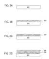
- FIG. 1is a flow chart of one embodiment of a method 100 of forming a fluorinated high-K dielectric layer on a substrate surface.
- FIGS. 2A-2Dcorrespond to method 100 to illustrate the formation of a dielectric material used in a semiconductor devices, such as a transistor or a capacitor.
- a high-K dielectric layer 202is formed on a substrate 201 .
- the substrate 201is exposed to a plasma comprising a fluorine source to form a fluorinated high-k dielectric layer 204 .
- a gate electrode 206is formed on the substrate 201 .
- the high-K dielectric layer 202 of step 110may be deposited on a substrate by conventional deposition techniques such as atomic layer deposition (ALD), chemical vapor deposition (CVD), physical vapor deposition (PVD), thermal and plasma techniques and combinations thereof.
- ALDatomic layer deposition
- CVDchemical vapor deposition
- PVDphysical vapor deposition
- thermal and plasma techniques and combinations thereofare conventional deposition techniques.
- the high-k dielectric layer 202is deposited by an ALD process and apparatus, such as described in co-pending United States Patent Application Publication No. 2005/0271812, published Dec. 8, 2005, entitled, “Apparatuses And Methods For Atomic Layer Deposition of Hafnium-containing High-K Dielectric Materials,” assigned to Applied Materials, Inc., and herein incorporated by reference.
- the high-k dielectric layer 202is generally deposited with a film thickness from about 10 ⁇ to about 1000 ⁇ , preferably from about 20 ⁇ to about 500 ⁇ and more preferably from about 50 ⁇ to about 200 ⁇ , for example, about 100 ⁇ .
- An optional pre-clean stepmay be performed prior to deposition of the high-k dielectric layer 202 on the substrate 201 .
- suitable high-k deposition chambersinclude the FLEXSTAR®, which is commercially available from Applied Materials, Inc., Santa Clara, Calif.
- the substrateis bombarded with atomic-F formed by co-flowing F 2 and an inert gas plasma such as argon.
- an inert gas plasmasuch as argon.
- F 2other fluorine-containing gases may be used to form the fluorine plasma, such as NF 3 , HF, or combinations thereof.
- F 2other fluorine-containing gases
- inert gasesinclude helium, neon, and xenon.
- gasessuch as nitrogen and oxygen may be used in place of or in combination with the inert gases.
- the gases used in this processare carbon free.
- the fluorination processproceeds at a time period from about 10 seconds to about 360 seconds, preferably from about 30 seconds to about 180 seconds, for example, about 120 seconds.
- the fluorination processgenerally occurs at a temperature less than 100° C., for example, between about 50° C. and less than 100° C.
- the fluorination processis conducted with a plasma power setting from about 50 watts to about 2,500, for example between about 50 watts to about 1000 watts, such as between about 70 watts to 200 watts and a pressure from about 10 mTorr to about 100 mTorr.
- the fluorinehas a flow rate from about 0.1 slm to about 1.0 slm.
- the individual and total gas flows of the processing gasesmay vary based upon a number of processing factors, such as the size of the processing chamber, the temperature of the processing chamber, and the size of the substrate being processed.
- the fluorination processuses moderate density low ion energy fluorine plasma.
- Low ion energy pulsed fluorine bearing plasmasallow for the incorporation of fluorine into high-k gate stacks without sufficient energy for ion etching.
- the concentration of fluorine in the fluorinated dielectric layeris between 1E14 atoms/cm 2 and 4E15 atoms/cm 2 .
- plasma fluorinationis performed in a chamber with pressure ranging from about 5-20 mTorr or 10-20 mTorr, with a plasma power of 200-800 Watts, for example, between about 250 watts and about 600 watts.
- the fluorine gasmay be flown into the chamber at a flow rate ranging from about 100-200 sccm.
- the plasma fluorinationuses a pulse radio frequency plasma process at about 10-20 MHz and pulse at about 5-15 kHz.
- the plasma fluorination process parameterscan be modified depending on the chamber size and volume, and the desired thickness of the dielectric film.
- An optional anneal stepmay be performed prior to or after the plasma fluorination process.
- the plasma fluorination process parametersare selected so that sufficient energy for etching of the dielectric is not available.
- the gate electrode 206 of step 130may be deposited on the substrate 201 after the structure is exposed to the plasma and annealed, a gate electrode 206 , such as a polysilicon layer, an amorphous silicon layer, or a metal layer, such as titanium, titanium nitride, tantalum, tantalum nitride, tungsten, tungsten nitride, and other refractory metals or other suitable electrode materials may be deposited on the fluorinated high-k dielectric layer 204 .
- a gate electrode 206such as a polysilicon layer, an amorphous silicon layer, or a metal layer, such as titanium, titanium nitride, tantalum, tantalum nitride, tungsten, tungsten nitride, and other refractory metals or other suitable electrode materials may be deposited on the fluorinated high-k dielectric layer 204 .
- FIG. 3is a schematic diagram of a plasma process reactor 300 , made by Applied Materials, Inc., located in Santa Clara, Calif. It is an inductive plasma source reactor that is one example of a reactor that may be used to practice the present invention.
- the reactor 300comprises a process chamber 310 having an electrostatic chuck 316 within a conductive body (wall) 330 , and a controller 340 .
- the chamber 310is supplied with a substantially flat dielectric ceiling 320 .
- Other modifications of the chamber 310may have other types of ceilings, e.g., a dome-shaped ceiling.
- Above the ceiling 320is disposed an antenna comprising at least one inductive coil element 312 (two co-axial elements 312 are shown).
- the inductive coil element 312is coupled, through a first matching network 319 , to a plasma power source 318 .
- the plasma power source 318typically is capable of producing up to 3000 W at a tunable frequency in a range, for example, from 50 kHz to 13.56 MHz.
- the electrostatic chuck 316includes a first electrode 354 and a second electrode 356 embedded in a dielectric material.
- the first electrode 354 and second electrode 356are biased with DC potentials to provide the chucking action that holds the substrate 314 .
- Application of the chucking voltage to the electrostatic chuck 316 and wafer spacing maskproduces charge distribution along the underside of the substrate 314 and over the surface of the electrostatic chuck 316 .
- the opposite polarity of these chargesproduces an attractive electrostatic force between the substrate 314 and the electrostatic chuck 316 . This force retains the substrate 314 upon the chuck 316 without relying upon a plasma within the processing chamber 310 to provide a conductive grounding path for the substrate 314 .
- the electrostatic chuck 316may also be a monopolar chuck.
- the electrostatic chuck 316is coupled, through a second matching network 324 , to a biasing power source 322 .
- the biasing power source 322is generally capable of producing a RF signal having a tunable frequency of 50 kHz to 13.56 MHz and a power of between 0 and 5000 watts.
- the biasing power source 322may be a DC or pulsed DC source.
- a controller 340comprising a central processing unit (CPU) 344 , a memory 342 , and support circuits 346 for the CPU 344 and facilitates control of the components of the chamber 310 and, as such, of the nitridation process as discussed.
- the voltage for operating the electrostatic chuck 316can be supplied by a separate “chuck” power supply (not shown).
- One output terminal of the chucking power supplyis connected to the chuck electrode.
- the other output terminaltypically is connected to electrical ground, but alternatively may be connected to a metal body portion of the electrostatic chuck 316 .
- the substrateis placed in contact with the dielectric material, and a direct current voltage is placed on the electrode to create the electrostatic attractive force or bias to adhere the substrate on the upper surface of the electrostatic chuck 316 .
- a semiconductor wafer 314is placed on the electrostatic chuck 316 and process gases are supplied from a gas panel 338 through entry ports 326 to form a gaseous mixture 350 .
- the gaseous mixture 350is ignited to form a plasma 355 in the chamber 310 by applying power from the plasma power source 318 .
- the pressure within the interior of the chamber 310is controlled using a throttle valve 327 and a vacuum pump 336 .
- the chamber wall 330is coupled to an electrical ground 334 .
- the temperature of the wall 330is controlled using liquid-containing conduits (not shown) that run through the wall 330 .
- the temperature of the substrate 314is controlled by stabilizing a temperature of the electrostatic chuck 316 .
- helium gas from a gas source 348is provided via a gas conduit 349 to channels (not shown) formed in the surface of the electrostatic chuck 316 to a fine space (not shown) formed between the reverse surface of the substrate 314 and the upper surface of the electrostatic chuck 316 .
- the electrostatic chuck 316may be heated by a resistive heater (not shown) within the pedestal of the electrostatic chuck 316 to a steady state temperature and then the helium gas facilitates uniform heating of the substrate 314 .
- the controller 340may be one of any form of general-purpose, computer processor that can be used in an industrial setting for controlling various chambers and sub-processors.
- the memory 342 , or computer-readable medium, of the CPU 344may be one or more of readily available memory such as random access memory (RAM), read only memory (ROM), floppy disk, hard disk, or any other form of digital storage, local or remote.
- the support circuits 346are coupled to the CPU 344 for supporting the processor in a conventional manner. These circuits include cache, power supplies, clock circuits, input/output circuitry and subsystems, and the like.
- the inventive methodis generally stored in the memory 342 as a software routine.
- the software routinemay also be stored and/or executed by a second CPU (not shown) that is remotely located from the hardware being controlled by the CPU 344 .
- Decoupled Plasma Nitridation process reactor 300Other details of the Decoupled Plasma Nitridation process reactor 300 are described in U.S. Patent Application Publication No. 2004/0242021, entitled “Method and Apparatus for Plasma Nitridation of Gate Dielectrics Using Amplitude Modulated Radio Frequency Energy,” assigned to Applied Materials, Inc., published Dec. 2, 2004, issued as U.S. Pat. No. 7,179,754, and herein incorporated by reference to the extent not inconsistent with the invention.
- suitable DPN chambersinclude the DPN CenturaTM, which is commercially available from Applied Materials, Inc., Santa Clara, Calif.
- Other suitable plasma chambersinclude the P3i chamber, which is also commercially available form Applied Materials, Inc.
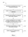
- FIG. 4is a flow diagram of a method 400 in accordance with one embodiment of the present invention.
- the surface of the substratemay be cleaned to remove native oxides which may have formed on the surface of the substrate.
- the processstarts with introducing a silicon substrate into a first processing chamber at step 402 .
- About 5 ⁇ to about 100 ⁇ of hafnium silicate (HfSiO x )is grown on a silicon wafer at step 404 .
- HfSiO xhafnium silicate
- hafnium silicate layeris one example of a material deposited using this method.
- the inventioncan be applied to other types of gate dielectrics, which could be a high-K dielectric material having a dielectric constant greater than 4.0.
- the inventionmay also be applied to silicon oxynitrides.
- the substratemay be transferred to an anneal chamber, such as the CENTURATM RADIANCETM rapid thermal processing (RTP) chamber available from Applied Materials, Inc., located in Santa Clara, Calif., for a post deposition annealing of the HfSiO x film.
- RTPrapid thermal processing
- a post deposition annealmay be performed where the substrate is annealed at a temperature from about 500° C. to about 1200° C., preferably from about 550-700° C. for a time period from about 1 second to about 240 seconds, preferably from about 30 seconds to about 90 seconds, for example, at about 650° C. for about 60 seconds.
- the anneal chamber atmospherecontains at least one anneal gas, such as O 2 , N 2 , NH 3 , N 2 H 4 , NO, N 2 O, or combinations thereof.
- the anneal chamberis maintained at a pressure from about 5 Torr to about 100 Torr, for example, at about 50 Torr.
- the substrateis then transferred into a plasma chamber containing at least a fluorine-containing gas.
- the fluorination processuses moderate density low ion energy fluorine plasma.
- Low ion energy pulsed fluorine bearing plasmasallow for the incorporation of fluorine into high-k gate stacks without sufficient energy for ion etching.
- the fluorination processmay be performed using an inductive pulse plasma, a capacitive source plasma, or continuous wave mixed inductive and capacitive source plasma.
- the substrateis transferred back to the RTP processing chamber where a post fluorination anneal step is performed.
- the substrateis annealed at a temperature from about 600° C. to about 1200° C., preferably from about 700-1100° C. for a time period from about 1 second to about 120 seconds, preferably from about 30 seconds to about 90 seconds, for example, at about 1000° C. for about 60 seconds.
- the anneal chamber atmospherecontains at least one anneal gas, such as O 2 , N 2 , NH 3 , N 2 H 4 , NO, N 2 O, or combinations thereof.
- the anneal chamberis maintained at a pressure from about 5 Torr to about 100 Torr, for example, at about 15 Torr.
- the post fluorination annealcomprises a two-step process in which an inert or reducing step is followed by an oxidizing step.
- a gate electrodesuch as polysilicon may be deposited by low pressure chemical vapor deposition (LPCVD), atomic layer epitaxy (ALE), thermal decomposition methods, or other methods known in the art.
- LPCVDlow pressure chemical vapor deposition
- ALEatomic layer epitaxy
- the polysilicon layergenerally contains dopants such as boron, phosphorous or arsenic.
- the gate electrodecan also be a metal layer.
- FIG. 5is a schematic view of an integrated processing system 500 capable of performing the processes disclosed herein.
- the integrated system 500comprises a cleaning module 510 and a thermal processing/deposition mainframe system 530 .
- the cleaning module 510is an OASIS CLEANTM system, available from Applied Materials, Inc., located in Santa Clara, Calif.
- the thermal processing/deposition mainframe system 530is a CENTURA® system and is also commercially available from Applied Materials, Inc., located in Santa Clara, Calif. This particular embodiment of the system to perform the process as disclosed herein is provided to illustrate the invention and should not be used to limit the scope of the invention.
- the cleaning module 510generally includes one or more substrate cassettes 512 , one or more transfer robots 514 disposed in a substrate transfer region, and one or more single-substrate clean chambers 516 .
- Other aspects and embodiments of a single-substrate clean systemare disclosed in U.S. Patent Application Publication No. 2002/0029788, published Mar. 14, 2002, entitled “Method and Apparatus for Wafer Cleaning” and in U.S. Patent Application Publication No. 2002/0063169, published May 30, 2002, entitled “Wafer Spray Configurations for a Single Wafer Processing Apparatus,” both of which are herein incorporated by reference in their entirety to the extent not inconsistent with the present disclosure.
- the thermal processing/deposition mainframe system 530generally includes load lock chambers 532 , a transfer chamber 534 , and processing chambers 536 A, 536 B, 536 C, and 536 D.
- the transfer chamber 534is preferably between 1 mTorr to about 100 Torr and preferably comprises a non-reactive gas ambient, such as a N 2 ambient.
- the load lock chambers 532allow for the transfer of substrates into and out from the thermal processing/deposition mainframe system 530 while the transfer chamber 534 remains under a low pressure non-reactive environment.
- the transfer chamberincludes a robot 540 having one or more blades which transfers the substrates between the load lock chambers 532 and processing chambers 536 A, 536 B, 536 C, and 536 D. Any of the processing chambers 536 A, 536 B, 536 C, or 536 D may be removed from the thermal processing/deposition mainframe system 530 if not necessary for the particular process to be performed by the system 530 .
- the pre-treatment stepmay include polishing, etching, reduction, oxidation, hydroxylation, annealing and/or baking. Exposing the substrate to air between the pre-treatment step and the high-K dielectric layer formation may reduce the effectiveness of nucleation thereover of high-K dielectric materials. It is optional to have the cleaning module 510 coupled with mainframe system 530 as shown in FIG. 5 to further reduce the formation of native oxides over and/or contamination of substrates between cleaning steps and other processing steps. Of course, in other embodiments, cleaning steps may be performed in a cleaning module separate from the thermal processing/deposition mainframe system.
- processing chamber 536 Aadapted to perform the fluorination process as described above
- processing chamber 536 Badapted to perform a process such as a chemical vapor deposition chamber or an atomic layer deposition chamber, adapted to deposit a high dielectric constant material, such as a hafnium containing layer.
- processing chamber 536 Ccomprises a rapid thermal processing (RTP) chamber where the structure may be annealed.
- the RTP chambermay be a XE, XE Plus or Radiance chamber available from Applied Materials, Inc.
- processing chamber 536 Dcomprises a low pressure chemical vapor deposition chamber (LPCVD), such as a POLYgen chamber, available from Applied Materials, Inc, adapted to deposit a gate dielectric layer.
- LPCVDlow pressure chemical vapor deposition chamber
- POLYgen chamberavailable from Applied Materials, Inc
- processing chamber 536 Dcomprises a low pressure chemical vapor deposition chamber (LPCVD), such as a POLYgen chamber, available from Applied Materials, Inc, adapted to deposit a gate dielectric layer.
- LPCVDlow pressure chemical vapor deposition chamber
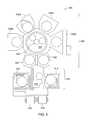
- FIG. 6is an isometric cross-sectional view of one embodiment of a plasma chamber 1 that may be configured for a plasma enhanced chemical vapor deposition (PECVD) process, a high density plasma chemical vapor deposition (HDPCVD) process, an ion implantation process, an etch process, and other plasma processes.
- the plasma chamber 1includes a torodial plasma source 600 coupled to a body 3 of the chamber 1 .
- the body 3includes sidewalls 5 coupled to a lid 10 and a bottom 15 , which bounds an interior volume 20 .
- Other examples of a plasma chamber 1may be found in U.S. Pat. No. 6,939,434, filed Jun. 5, 2002 and issued on Sep. 6, 2005 and U.S. Pat. No. 6,893,907, filed Feb. 24, 2004 and issued May 17, 2005, both of which are incorporated by reference herein in their entireties.
- the interior volume 20includes a processing region 25 formed between a showerhead 700 and a substrate support 800 .
- a pumping region 30surrounds a portion of the substrate support 800 .
- the pumping region 30is in selective communication with a vacuum pump 40 by a valve 35 disposed in a port 45 formed in the bottom 15 .
- the valve 35is a throttle valve that is adapted to control the flow of gas or vapor from the interior volume 20 and through the port 45 to the vacuum pump 40 .
- the valve 35operates without the use of o-rings, and is further described in United States Patent Publication No. 2006/0237136, filed Apr. 26, 2005, which is incorporated by reference in its entirety.
- the torodial plasma source 600includes a first conduit 650 A having a general “U” shape, and a second conduit 650 B having a general “M” shape.
- the first conduit 650 A and the second conduit 650 Beach include at least one antenna 670 A, 670 B that are used to form an inductively coupled plasma within an interior region 655 A, 655 B of each of the conduits 650 A, 650 B, respectively.
- Each antenna 670 A, 670 Bmay be a winding or a coil coupled to a power source, such as a RF power sources 671 A, 672 A.
- RF impedance matching systems 671 B, 672 Bmay also be coupled to each antenna 670 A, 670 B.
- Process gasessuch as helium, argon, and other gases, may be provided to an interior region 655 A, 655 B of each of the conduits 650 A, 650 B, respectively.
- the process gasesmay contain a dopant containing gases that is supplied to the interior regions 655 A, 655 B of each conduit 650 A, 650 B.
- the process gasis delivered from a gas source 630 A that is connected to a port 55 formed in the body 3 of the chamber 1 .
- each opposing end of the conduits 650 A, 650 Bare coupled to respective ports (ports 50 A and 50 B for conduit 650 B are shown in this view) formed in the lid 10 of the chamber 1 .
- a process gasis supplied to the interior region 655 A, 655 B of each of the conduits 650 A, 650 B, and RF power is applied to each antenna 670 A, 670 B, to generate a circulating plasma path that travels through the ports, e.g. 50 A- 50 B and the processing region 25 .
- the circulating plasma pathtravels through port 50 A to port 50 B, or visa versa, through the processing region 25 between the gas distribution assembly 700 and substrate support 800 .
- Each conduit 650 A, 650 Bincludes a plasma channeling means 606 coupled between respective ends of the conduit and the ports, e.g. 50 A- 50 B, which is configured to split and widen the plasma path formed within each of the conduits 650 A, 650 B.
- the gas distribution plate 700includes an annular wall 710 defining a plenum 730 between the lid 10 and a perforated plate 720 .
- the perforated plate 720includes a plurality of openings formed through the plate in a symmetrical or non-symmetrical pattern or patterns.
- Process gasessuch as dopant-containing gases, may be provided to the plenum 730 from the port 55 .
- the dopant-containing gasis a chemical consisting of the dopant impurity atom, such as boron (a p-type conductivity impurity in silicon) or phosphorus (an n-type conductivity impurity in silicon) and a volatile species such as fluorine and/or hydrogen.
- fluorides and/or hydrides of boron, phosphorous, or other dopant speciessuch as, arsenic, antimony, etc.
- the dopant-containing gasmay contain boron trifluoride (BF 3 ) or diborane (B 2 H 6 ).
- the gasesmay flow through the openings and into the processing region 25 below the perforated plate 720 .
- the perforated plateis RF biased to help generate and/or maintain a plasma in the processing region 25 .
- the substrate support 800generally includes an upper layer or puck 810 and a cathode assembly 820 .
- the puck 810includes a smooth substrate supporting surface and an embedded electrode 815 that can be biased by use of DC power source 806 to facilitate electrostatic attraction between a substrate and the substrate supporting surface of the puck 810 .
- the embedded electrode 815may also be used as an electrode that provides RF energy to the processing region 25 and form an RF bias during processing.
- the embedded electrode 815may be coupled to a RF power source 805 A and may also include an impedance match 805 B.
- the substrate support 800is a substrate contact-cooling electrostatic chuck in which the portion of the chuck contacting the substrate is cooled. The cooling is provided by coolant channels (not shown) disposed in the cathode assembly 820 for circulating a coolant therein.
- the substrate support 800may also include a lift pin assembly 900 that contains a plurality of lift pins 910 (only one is shown in this view).
- the lift pins 910facilitate transfer of one or more substrates by selectively lifting and supporting a substrate above the puck 810 , and are spaced to allow a robot blade (not shown) to positioned therebetween.
- the lift pin assemblies 900contain bushings 920 that are coupled to one or both of the puck 810 and the cathode assembly 820 .
- FIGS. 4 , 5 , and 6While the above embodiments are described with respect to FIGS. 4 , 5 , and 6 , it is recognized that other integrated processing systems and chamber combinations may be used with the embodiments described herein. Furthermore, any number of processing chambers may be part of a non-integrated system.
Landscapes
- Engineering & Computer Science (AREA)
- Microelectronics & Electronic Packaging (AREA)
- Condensed Matter Physics & Semiconductors (AREA)
- General Physics & Mathematics (AREA)
- Manufacturing & Machinery (AREA)
- Computer Hardware Design (AREA)
- Physics & Mathematics (AREA)
- Power Engineering (AREA)
- Chemical & Material Sciences (AREA)
- Chemical Kinetics & Catalysis (AREA)
- Crystallography & Structural Chemistry (AREA)
- General Chemical & Material Sciences (AREA)
- Chemical Vapour Deposition (AREA)
- Formation Of Insulating Films (AREA)
Abstract
Description
Claims (18)
Priority Applications (1)
| Application Number | Priority Date | Filing Date | Title |
|---|---|---|---|
| US11/861,578US7902018B2 (en) | 2006-09-26 | 2007-09-26 | Fluorine plasma treatment of high-k gate stack for defect passivation |
Applications Claiming Priority (2)
| Application Number | Priority Date | Filing Date | Title |
|---|---|---|---|
| US82702306P | 2006-09-26 | 2006-09-26 | |
| US11/861,578US7902018B2 (en) | 2006-09-26 | 2007-09-26 | Fluorine plasma treatment of high-k gate stack for defect passivation |
Publications (2)
| Publication Number | Publication Date |
|---|---|
| US20080076268A1 US20080076268A1 (en) | 2008-03-27 |
| US7902018B2true US7902018B2 (en) | 2011-03-08 |
Family
ID=39230940
Family Applications (1)
| Application Number | Title | Priority Date | Filing Date |
|---|---|---|---|
| US11/861,578Active2029-05-08US7902018B2 (en) | 2006-09-26 | 2007-09-26 | Fluorine plasma treatment of high-k gate stack for defect passivation |
Country Status (4)
| Country | Link |
|---|---|
| US (1) | US7902018B2 (en) |
| JP (1) | JP5590886B2 (en) |
| TW (1) | TWI435376B (en) |
| WO (1) | WO2008039845A2 (en) |
Cited By (6)
| Publication number | Priority date | Publication date | Assignee | Title |
|---|---|---|---|---|
| US8658490B2 (en)* | 2012-04-04 | 2014-02-25 | Globalfoundries Inc. | Passivating point defects in high-K gate dielectric layers during gate stack formation |
| US8735305B2 (en) | 2012-05-24 | 2014-05-27 | Intermolecular, Inc. | Methods of forming fluorinated hafnium oxide gate dielectrics by atomic layer deposition |
| US8821985B2 (en) | 2012-11-02 | 2014-09-02 | Intermolecular, Inc. | Method and apparatus for high-K gate performance improvement and combinatorial processing |
| US8945414B1 (en) | 2013-11-13 | 2015-02-03 | Intermolecular, Inc. | Oxide removal by remote plasma treatment with fluorine and oxygen radicals |
| US9275993B2 (en) | 2012-09-07 | 2016-03-01 | Samsung Electronics Co., Ltd. | Semiconductor device and method for fabricating the same |
| US11239258B2 (en)* | 2016-07-19 | 2022-02-01 | Applied Materials, Inc. | High-k dielectric materials comprising zirconium oxide utilized in display devices |
Families Citing this family (26)
| Publication number | Priority date | Publication date | Assignee | Title |
|---|---|---|---|---|
| KR100788361B1 (en)* | 2006-12-12 | 2008-01-02 | 동부일렉트로닉스 주식회사 | Formation method of MOSFET device |
| KR100877100B1 (en)* | 2007-04-16 | 2009-01-09 | 주식회사 하이닉스반도체 | Nonvolatile Memory Device Manufacturing Method |
| JP2010199294A (en)* | 2009-02-25 | 2010-09-09 | Toshiba Corp | Semiconductor device |
| US9685186B2 (en)* | 2009-02-27 | 2017-06-20 | Applied Materials, Inc. | HDD pattern implant system |
| US9048186B2 (en)* | 2009-10-08 | 2015-06-02 | Taiwan Semiconductor Manufacturing Company, Ltd. | Methods for forming integrated circuits |
| WO2012083220A2 (en)* | 2010-12-16 | 2012-06-21 | The Regents Of The University Of California | Generation of highly n-type, defect passivated transition metal oxides using plasma fluorine insertion |
| US8802545B2 (en)* | 2011-03-14 | 2014-08-12 | Plasma-Therm Llc | Method and apparatus for plasma dicing a semi-conductor wafer |
| US8952458B2 (en)* | 2011-04-14 | 2015-02-10 | Taiwan Semiconductor Manufacturing Company, Ltd. | Gate dielectric layer having interfacial layer and high-K dielectric over the interfacial layer |
| US9006092B2 (en)* | 2011-11-03 | 2015-04-14 | United Microelectronics Corp. | Semiconductor structure having fluoride metal layer and process thereof |
| CN103959380B (en) | 2011-11-23 | 2017-08-29 | 应用材料公司 | Method for photoresist planarization by chemical vapor deposition of silicon oxide |
| WO2013111040A1 (en)* | 2012-01-27 | 2013-08-01 | Koninklijke Philips N.V. | Capacitive micro-machined transducer and method of manufacturing the same |
| JP6146874B2 (en)* | 2012-03-28 | 2017-06-14 | 株式会社日立国際電気 | Semiconductor device manufacturing method, substrate processing method, substrate processing apparatus, and program |
| US8791003B2 (en)* | 2012-06-21 | 2014-07-29 | GlobalFoundries, Inc. | Methods for fabricating integrated circuits with fluorine passivation |
| WO2014058452A1 (en)* | 2012-10-12 | 2014-04-17 | Lawrence Livermore National Security, Llc | Planarization of optical substrates |
| US8981466B2 (en)* | 2013-03-11 | 2015-03-17 | International Business Machines Corporation | Multilayer dielectric structures for semiconductor nano-devices |
| CN103295890B (en)* | 2013-05-30 | 2015-12-09 | 北京大学 | Be deposited on the processing method of the gate medium on germanium base or three or five compounds of group base substrates |
| US9245793B2 (en)* | 2013-12-19 | 2016-01-26 | Intermolecular, Inc. | Plasma treatment of low-K surface to improve barrier deposition |
| US10134878B2 (en)* | 2016-01-14 | 2018-11-20 | Applied Materials, Inc. | Oxygen vacancy of IGZO passivation by fluorine treatment |
| US10580643B2 (en)* | 2016-02-16 | 2020-03-03 | Applied Materials, Inc. | Fluorination during ALD high-k, fluorination post high-k and use of a post fluorination anneal to engineer fluorine bonding and incorporation |
| US20180033619A1 (en)* | 2016-07-29 | 2018-02-01 | Applied Materials, Inc. | Performing decoupled plasma fluorination to reduce interfacial defects in film stack |
| US10134873B2 (en)* | 2016-11-18 | 2018-11-20 | Taiwan Semiconductor Manufacturing Co., Ltd. | Semiconductor device gate structure and method of fabricating thereof |
| US10431462B2 (en)* | 2017-02-15 | 2019-10-01 | Lam Research Corporation | Plasma assisted doping on germanium |
| US10629749B2 (en)* | 2017-11-30 | 2020-04-21 | Taiwan Semiconductor Manufacturing Co., Ltd. | Method of treating interfacial layer on silicon germanium |
| US11380536B2 (en)* | 2020-05-05 | 2022-07-05 | Applied Materials, Inc. | Multi-step pre-clean for selective metal gap fill |
| US11501972B2 (en) | 2020-07-22 | 2022-11-15 | Applied Materials, Inc. | Sacrificial capping layer for passivation using plasma-based implant process |
| US20230317634A1 (en)* | 2022-04-05 | 2023-10-05 | Applied Materials, Inc. | Coatings with diffusion barriers for corrosion and contamination protection |
Citations (260)
| Publication number | Priority date | Publication date | Assignee | Title |
|---|---|---|---|---|
| US3427514A (en) | 1966-10-13 | 1969-02-11 | Rca Corp | Mos tetrode |
| US3594295A (en) | 1966-09-19 | 1971-07-20 | Physics Technology Lab Inc | Rf sputtering of insulator materials |
| US4043848A (en) | 1971-04-30 | 1977-08-23 | Texas Instruments Incorporated | Method of fabrication of insulated gate field effect semiconductor devices |
| US4096509A (en) | 1976-07-22 | 1978-06-20 | The United States Of America As Represented By The Secretary Of The Air Force | MNOS memory transistor having a redeposited silicon nitride gate dielectric |
| US4262631A (en) | 1979-10-01 | 1981-04-21 | Kubacki Ronald M | Thin film deposition apparatus using an RF glow discharge |
| US4310380A (en) | 1980-04-07 | 1982-01-12 | Bell Telephone Laboratories, Incorporated | Plasma etching of silicon |
| US4335391A (en) | 1978-12-11 | 1982-06-15 | Texas Instruments Incorporated | Non-volatile semiconductor memory elements and methods of making |
| US4412119A (en) | 1980-05-14 | 1983-10-25 | Hitachi, Ltd. | Method for dry-etching |
| US4439463A (en) | 1982-02-18 | 1984-03-27 | Atlantic Richfield Company | Plasma assisted deposition system |
| US4459739A (en) | 1981-05-26 | 1984-07-17 | Northern Telecom Limited | Thin film transistors |
| US4495219A (en) | 1981-10-09 | 1985-01-22 | Fujitsu Limited | Process for producing dielectric layers for semiconductor devices |
| US4534826A (en) | 1983-12-29 | 1985-08-13 | Ibm Corporation | Trench etch process for dielectric isolation |
| US4545112A (en) | 1983-08-15 | 1985-10-08 | Alphasil Incorporated | Method of manufacturing thin film transistors and transistors made thereby |
| US4563367A (en) | 1984-05-29 | 1986-01-07 | Applied Materials, Inc. | Apparatus and method for high rate deposition and etching |
| US4585516A (en) | 1985-03-04 | 1986-04-29 | Tegal Corporation | Variable duty cycle, multiple frequency, plasma reactor |
| US4605947A (en) | 1983-03-07 | 1986-08-12 | Motorola Inc. | Titanium nitride MOS device gate electrode and method of producing |
| US4608063A (en) | 1983-11-25 | 1986-08-26 | Canon Kabushiki Kaisha | Exhaust system for chemical vapor deposition apparatus |
| US4651185A (en) | 1983-08-15 | 1987-03-17 | Alphasil, Inc. | Method of manufacturing thin film transistors and transistors made thereby |
| US4700458A (en) | 1981-07-27 | 1987-10-20 | Tokyo Shibaura Denki Kabushiki Kaisha | Method of manufacture thin film transistor |
| US4725560A (en) | 1986-09-08 | 1988-02-16 | International Business Machines Corp. | Silicon oxynitride storage node dielectric |
| US4743953A (en) | 1980-12-29 | 1988-05-10 | Fujitsu Limited | Random access memory cell with MIS capacitor having insulator of oxide of doped metal |
| US4745082A (en) | 1986-06-12 | 1988-05-17 | Ford Microelectronics, Inc. | Method of making a self-aligned MESFET using a substitutional gate with side walls |
| US4851370A (en) | 1987-12-28 | 1989-07-25 | American Telephone And Telegraph Company, At&T Bell Laboratories | Fabricating a semiconductor device with low defect density oxide |
| US4913929A (en) | 1987-04-21 | 1990-04-03 | The Board Of Trustees Of The Leland Stanford Junior University | Thermal/microwave remote plasma multiprocessing reactor and method of use |
| US4948458A (en) | 1989-08-14 | 1990-08-14 | Lam Research Corporation | Method and apparatus for producing magnetically-coupled planar plasma |
| US4980307A (en) | 1978-06-14 | 1990-12-25 | Fujitsu Limited | Process for producing a semiconductor device having a silicon oxynitride insulative film |
| US5000113A (en) | 1986-12-19 | 1991-03-19 | Applied Materials, Inc. | Thermal CVD/PECVD reactor and use for thermal chemical vapor deposition of silicon dioxide and in-situ multi-step planarized process |
| US5063431A (en) | 1987-07-31 | 1991-11-05 | Kabushiki Kaisha Toshiba | Semiconductor device having a two-layer gate structure |
| EP0232619B1 (en) | 1985-12-26 | 1992-03-25 | Canon Kabushiki Kaisha | Method of manufacturing a thin-film transistor |
| US5173442A (en) | 1990-07-23 | 1992-12-22 | Microelectronics And Computer Technology Corporation | Methods of forming channels and vias in insulating layers |
| US5228950A (en) | 1990-12-04 | 1993-07-20 | Applied Materials, Inc. | Dry process for removal of undesirable oxide and/or silicon residues from semiconductor wafer after processing |
| US5292673A (en) | 1989-08-16 | 1994-03-08 | Hitachi, Ltd | Method of manufacturing a semiconductor device |
| US5302236A (en) | 1990-10-19 | 1994-04-12 | Tokyo Electron Limited | Method of etching object to be processed including oxide or nitride portion |
| US5314724A (en) | 1991-01-08 | 1994-05-24 | Fujitsu Limited | Process for forming silicon oxide film |
| US5335138A (en) | 1993-02-12 | 1994-08-02 | Micron Semiconductor, Inc. | High dielectric constant capacitor and method of manufacture |
| US5391510A (en) | 1992-02-28 | 1995-02-21 | International Business Machines Corporation | Formation of self-aligned metal gate FETs using a benignant removable gate material during high temperature steps |
| US5464783A (en) | 1993-03-24 | 1995-11-07 | At&T Corp. | Oxynitride-dioxide composite gate dielectric process for MOS manufacture |
| US5582866A (en) | 1993-01-28 | 1996-12-10 | Applied Materials, Inc. | Single substrate vacuum processing apparatus having improved exhaust system |
| US5619051A (en) | 1994-06-27 | 1997-04-08 | Nec Corporation | Semiconductor nonvolatile memory cell |
| US5726087A (en) | 1992-04-30 | 1998-03-10 | Motorola, Inc. | Method of formation of semiconductor gate dielectric |
| US5763922A (en) | 1997-02-28 | 1998-06-09 | Intel Corporation | CMOS integrated circuit having PMOS and NMOS devices with different gate dielectric layers |
| EP0847079A2 (en) | 1996-12-05 | 1998-06-10 | Texas Instruments Incorporated | Method of manufacturing an MIS electrode |
| US5834343A (en) | 1995-08-31 | 1998-11-10 | Kabushiki Kaisha Toshiba | Method of manufacturing thin film transistor |
| US5840626A (en) | 1995-09-28 | 1998-11-24 | Kabushiki Kaisha Toshiba | Semiconductor device and method of manufacturing the same |
| US5851602A (en) | 1993-12-09 | 1998-12-22 | Applied Materials, Inc. | Deposition of high quality conformal silicon oxide thin films for the manufacture of thin film transistors |
| US5865896A (en) | 1993-08-27 | 1999-02-02 | Applied Materials, Inc. | High density plasma CVD reactor with combined inductive and capacitive coupling |
| US5874766A (en) | 1988-12-20 | 1999-02-23 | Matsushita Electric Industrial Co., Ltd. | Semiconductor device having an oxynitride film |
| US5880508A (en) | 1997-10-20 | 1999-03-09 | Texas Instruments--Acer Incorporated | MOSFET with a high permitivity gate dielectric |
| US5891798A (en) | 1996-12-20 | 1999-04-06 | Intel Corporation | Method for forming a High dielectric constant insulator in the fabrication of an integrated circuit |
| US5928732A (en) | 1993-12-28 | 1999-07-27 | Applied Materials, Inc. | Method of forming silicon oxy-nitride films by plasma-enhanced chemical vapor deposition |
| US5935373A (en) | 1996-09-27 | 1999-08-10 | Tokyo Electron Limited | Plasma processing apparatus |
| US5937303A (en) | 1997-10-29 | 1999-08-10 | Advanced Micro Devices | High dielectric constant gate dielectric integrated with nitrogenated gate electrode |
| US5960270A (en) | 1997-08-11 | 1999-09-28 | Motorola, Inc. | Method for forming an MOS transistor having a metallic gate electrode that is formed after the formation of self-aligned source and drain regions |
| US5976993A (en) | 1996-03-28 | 1999-11-02 | Applied Materials, Inc. | Method for reducing the intrinsic stress of high density plasma films |
| US6008095A (en) | 1998-08-07 | 1999-12-28 | Advanced Micro Devices, Inc. | Process for formation of isolation trenches with high-K gate dielectrics |
| US6013553A (en) | 1997-07-24 | 2000-01-11 | Texas Instruments Incorporated | Zirconium and/or hafnium oxynitride gate dielectric |
| US6020024A (en) | 1997-08-04 | 2000-02-01 | Motorola, Inc. | Method for forming high dielectric constant metal oxides |
| US6023613A (en) | 1996-12-10 | 2000-02-08 | Sony Corporation | Synthesizer receiver for automatically tuning master stations and associated satellite stations in specified geographical areas |
| US6027961A (en) | 1998-06-30 | 2000-02-22 | Motorola, Inc. | CMOS semiconductor devices and method of formation |
| US6033963A (en) | 1999-08-30 | 2000-03-07 | Taiwan Semiconductor Manufacturing Company | Method of forming a metal gate for CMOS devices using a replacement gate process |
| US6041734A (en) | 1997-12-01 | 2000-03-28 | Applied Materials, Inc. | Use of an asymmetric waveform to control ion bombardment during substrate processing |
| US6043157A (en) | 1997-12-18 | 2000-03-28 | Advanced Micro Devices | Semiconductor device having dual gate electrode material and process of fabrication thereof |
| TW386267B (en) | 1997-01-24 | 2000-04-01 | Applied Materials Inc | A high temperature, high flow rate chemical vapor deposition apparatus and related methods |
| US6049114A (en) | 1998-07-20 | 2000-04-11 | Motorola, Inc. | Semiconductor device having a metal containing layer overlying a gate dielectric |
| US6054013A (en) | 1996-02-02 | 2000-04-25 | Applied Materials, Inc. | Parallel plate electrode plasma reactor having an inductive antenna and adjustable radial distribution of plasma ion density |
| US6060755A (en) | 1999-07-19 | 2000-05-09 | Sharp Laboratories Of America, Inc. | Aluminum-doped zirconium dielectric film transistor structure and deposition method for same |
| US6063704A (en) | 1999-08-02 | 2000-05-16 | National Semiconductor Corporation | Process for incorporating silicon oxynitride DARC layer into formation of silicide polysilicon contact |
| US6066533A (en) | 1998-09-29 | 2000-05-23 | Advanced Micro Devices, Inc. | MOS transistor with dual metal gate structure |
| US6077403A (en) | 1997-06-06 | 2000-06-20 | Anelva Corporation | Sputtering device and sputtering method |
| US6083836A (en) | 1997-12-23 | 2000-07-04 | Texas Instruments Incorporated | Transistors with substitutionally formed gate structures and method |
| US6087231A (en) | 1999-08-05 | 2000-07-11 | Advanced Micro Devices, Inc. | Fabrication of dual gates of field transistors with prevention of reaction between the gate electrode and the gate dielectric with a high dielectric constant |
| US6090653A (en) | 1998-03-30 | 2000-07-18 | Texas Instruments | Method of manufacturing CMOS transistors |
| US6093590A (en) | 1999-09-14 | 2000-07-25 | Worldwide Semiconductor Manufacturing Corp. | Method of fabricating transistor having a metal gate and a gate dielectric layer with a high dielectric constant |
| US6110287A (en) | 1993-03-31 | 2000-08-29 | Tokyo Electron Limited | Plasma processing method and plasma processing apparatus |
| US6117279A (en) | 1998-11-12 | 2000-09-12 | Tokyo Electron Limited | Method and apparatus for increasing the metal ion fraction in ionized physical vapor deposition |
| US6130123A (en) | 1998-06-30 | 2000-10-10 | Intel Corporation | Method for making a complementary metal gate electrode technology |
| US6136654A (en) | 1996-06-07 | 2000-10-24 | Texas Instruments Incorporated | Method of forming thin silicon nitride or silicon oxynitride gate dielectrics |
| US6140024A (en) | 1997-12-31 | 2000-10-31 | Texas Instruments Incorporated | Remote plasma nitridation for contact etch stop |
| US6140688A (en) | 1998-09-21 | 2000-10-31 | Advanced Micro Devices Inc. | Semiconductor device with self-aligned metal-containing gate |
| US6171910B1 (en) | 1999-07-21 | 2001-01-09 | Motorola Inc. | Method for forming a semiconductor device |
| US6171900B1 (en) | 1999-04-15 | 2001-01-09 | Taiwan Semiconductor Manufacturing Company | CVD Ta2O5/oxynitride stacked gate insulator with TiN gate electrode for sub-quarter micron MOSFET |
| US6184114B1 (en) | 1999-08-17 | 2001-02-06 | Advanced Micro Devices, Inc. | MOS transistor formation |
| US6184072B1 (en) | 2000-05-17 | 2001-02-06 | Motorola, Inc. | Process for forming a high-K gate dielectric |
| US6190513B1 (en) | 1997-05-14 | 2001-02-20 | Applied Materials, Inc. | Darkspace shield for improved RF transmission in inductively coupled plasma sources for sputter deposition |
| US6200893B1 (en) | 1999-03-11 | 2001-03-13 | Genus, Inc | Radical-assisted sequential CVD |
| US6203613B1 (en) | 1999-10-19 | 2001-03-20 | International Business Machines Corporation | Atomic layer deposition with nitrate containing precursors |
| US6228229B1 (en) | 1995-11-15 | 2001-05-08 | Applied Materials, Inc. | Method and apparatus for generating a plasma |
| US6235650B1 (en) | 1997-12-29 | 2001-05-22 | Vanguard International Semiconductor Corporation | Method for improved semiconductor device reliability |
| US6244211B1 (en) | 1999-05-19 | 2001-06-12 | Mitsubishi Denki Kabushiki Kaisha | Plasma processing apparatus |
| US6254738B1 (en) | 1998-03-31 | 2001-07-03 | Applied Materials, Inc. | Use of variable impedance having rotating core to control coil sputter distribution |
| US6255231B1 (en) | 1998-10-02 | 2001-07-03 | Taiwan Semiconductor Manufacturing Co., Ltd | Method for forming a gate oxide layer |
| US6255698B1 (en) | 1999-04-28 | 2001-07-03 | Advanced Micro Devices, Inc. | Separately optimized gate structures for n-channel and p-channel transistors in an integrated circuit |
| US6254746B1 (en) | 1996-05-09 | 2001-07-03 | Applied Materials, Inc. | Recessed coil for generating a plasma |
| US6258675B1 (en) | 1997-12-18 | 2001-07-10 | Advanced Micro Devices, Inc. | High K gate electrode |
| US6277253B1 (en) | 1999-10-06 | 2001-08-21 | Applied Materials, Inc. | External coating of tungsten or tantalum or other refractory metal on IMP coils |
| US6287635B1 (en) | 1997-08-11 | 2001-09-11 | Torrex Equipment Corp. | High rate silicon deposition method at low pressures |
| US6291282B1 (en) | 1999-02-26 | 2001-09-18 | Texas Instruments Incorporated | Method of forming dual metal gate structures or CMOS devices |
| US6297107B1 (en) | 2000-10-19 | 2001-10-02 | Advanced Micro Devices, Inc. | High dielectric constant materials as gate dielectrics |
| US6297539B1 (en) | 1999-07-19 | 2001-10-02 | Sharp Laboratories Of America, Inc. | Doped zirconia, or zirconia-like, dielectric film transistor structure and deposition method for same |
| US6303481B2 (en) | 1999-12-29 | 2001-10-16 | Hyundai Electronics Industries Co., Ltd. | Method for forming a gate insulating film for semiconductor devices |
| US6320238B1 (en) | 1996-12-23 | 2001-11-20 | Agere Systems Guardian Corp. | Gate structure for integrated circuit fabrication |
| US6323555B1 (en) | 1998-01-28 | 2001-11-27 | Interuniversitiar Microelektronica Centrum (Imec Vzw) | Metallization structure on a fluorine-containing dielectric and a method for fabrication thereof |
| US20010049186A1 (en) | 1999-12-07 | 2001-12-06 | Effiong Ibok | Method for establishing ultra-thin gate insulator using anneal in ammonia |
| US20010055889A1 (en) | 1997-04-17 | 2001-12-27 | Ravi Iyer | Method for improving thickness uniformity of deposited ozone-TEOS silicate glass layers |
| US6344419B1 (en) | 1999-12-03 | 2002-02-05 | Applied Materials, Inc. | Pulsed-mode RF bias for sidewall coverage improvement |
| US6346465B1 (en) | 1997-06-23 | 2002-02-12 | Nec Corportion | Semiconductor device with silicide contact structure and fabrication method thereof |
| US6345588B1 (en) | 1997-08-07 | 2002-02-12 | Applied Materials, Inc. | Use of variable RF generator to control coil voltage distribution |
| US6348386B1 (en) | 2001-04-16 | 2002-02-19 | Motorola, Inc. | Method for making a hafnium-based insulating film |
| US6348126B1 (en) | 2000-08-11 | 2002-02-19 | Applied Materials, Inc. | Externally excited torroidal plasma source |
| US20020023900A1 (en) | 2000-08-18 | 2002-02-28 | Imad Mahawili | Chemistry for boron diffusion barrier layer and method of application in semiconductor device fabrication |
| US6352594B2 (en) | 1997-08-11 | 2002-03-05 | Torrex | Method and apparatus for improved chemical vapor deposition processes using tunable temperature controlled gas injectors |
| US6354593B1 (en) | 1999-11-10 | 2002-03-12 | Dror Frommer | Multi-level matching game and method |
| US6355108B1 (en) | 1999-06-22 | 2002-03-12 | Applied Komatsu Technology, Inc. | Film deposition using a finger type shadow frame |
| US6358810B1 (en) | 1998-07-28 | 2002-03-19 | Applied Materials, Inc. | Method for superior step coverage and interface control for high K dielectric capacitors and related electrodes |
| TW480569B (en) | 2000-03-08 | 2002-03-21 | Jusung Eng Co Ltd | High density plasma chemical vapor deposition apparatus and gap filling method using the same |
| US6361667B1 (en) | 1997-03-18 | 2002-03-26 | Anelva Corporation | Ionization sputtering apparatus |
| US6365450B1 (en) | 2001-03-15 | 2002-04-02 | Advanced Micro Devices, Inc. | Fabrication of P-channel field effect transistor with minimized degradation of metal oxide gate |
| US6365518B1 (en) | 2001-03-26 | 2002-04-02 | Applied Materials, Inc. | Method of processing a substrate in a processing chamber |
| US6373111B1 (en) | 1999-11-30 | 2002-04-16 | Intel Corporation | Work function tuning for MOSFET gate electrodes |
| US6376807B1 (en) | 1999-07-09 | 2002-04-23 | Applied Materials, Inc. | Enhanced cooling IMP coil support |
| US6399520B1 (en) | 1999-03-10 | 2002-06-04 | Tokyo Electron Limited | Semiconductor manufacturing method and semiconductor manufacturing apparatus |
| US20020066537A1 (en) | 1996-11-20 | 2002-06-06 | Satoshi Ogino | Plasma reactor |
| TW490765B (en) | 2000-02-10 | 2002-06-11 | Applied Materials Inc | A process and an integrated tool for low k dielectric deposition including a PECVD capping module |
| US6413382B1 (en) | 2000-11-03 | 2002-07-02 | Applied Materials, Inc. | Pulsed sputtering with a small rotating magnetron |
| US6420279B1 (en) | 2001-06-28 | 2002-07-16 | Sharp Laboratories Of America, Inc. | Methods of using atomic layer deposition to deposit a high dielectric constant material on a substrate |
| US6436801B1 (en) | 1999-02-26 | 2002-08-20 | Texas Instruments Incorporated | Hafnium nitride gate dielectric |
| US6444099B1 (en) | 1997-05-28 | 2002-09-03 | Anelva Corporation | Ionizing sputtering method |
| US6444592B1 (en) | 2000-06-20 | 2002-09-03 | International Business Machines Corporation | Interfacial oxidation process for high-k gate dielectric process integration |
| US6448166B2 (en) | 2000-06-30 | 2002-09-10 | Hynix Semiconductor Inc. | Method for forming a gate for semiconductor devices |
| US6447636B1 (en) | 2000-02-16 | 2002-09-10 | Applied Materials, Inc. | Plasma reactor with dynamic RF inductive and capacitive coupling control |
| US20020142624A1 (en) | 2000-09-19 | 2002-10-03 | Mattson Technology, Inc. | Method of forming dielectric films |
| US6461483B1 (en) | 2000-03-10 | 2002-10-08 | Applied Materials, Inc. | Method and apparatus for performing high pressure physical vapor deposition |
| US6472337B1 (en) | 2001-10-30 | 2002-10-29 | Sharp Laboratories Of America, Inc. | Precursors for zirconium and hafnium oxide thin film deposition |
| US6475854B2 (en) | 1999-12-30 | 2002-11-05 | Applied Materials, Inc. | Method of forming metal electrodes |
| US6475908B1 (en) | 2001-10-18 | 2002-11-05 | Chartered Semiconductor Manufacturing Ltd. | Dual metal gate process: metals and their silicides |
| US6477980B1 (en) | 2000-01-20 | 2002-11-12 | Applied Materials, Inc. | Flexibly suspended gas distribution manifold for plasma chamber |
| US6482752B1 (en) | 1993-10-26 | 2002-11-19 | Semiconductor Energy Laboratory Co., Ltd. | Substrate processing apparatus and method and a manufacturing method of a thin film semiconductor device |
| US6486080B2 (en) | 2000-11-30 | 2002-11-26 | Chartered Semiconductor Manufacturing Ltd. | Method to form zirconium oxide and hafnium oxide for high dielectric constant materials |
| US6497796B1 (en) | 1999-01-05 | 2002-12-24 | Novellus Systems, Inc. | Apparatus and method for controlling plasma uniformity across a substrate |
| US20020197883A1 (en) | 2001-06-20 | 2002-12-26 | Hiroaki Niimi | Method of ammonia annealing of ultra-thin silicon dioxide layers for uniform nitrogen profile |
| US6500742B1 (en) | 1994-11-14 | 2002-12-31 | Applied Materials, Inc. | Construction of a film on a semiconductor wafer |
| US6504214B1 (en) | 2002-01-11 | 2003-01-07 | Advanced Micro Devices, Inc. | MOSFET device having high-K dielectric layer |
| US6506287B1 (en) | 1998-03-16 | 2003-01-14 | Applied Materials, Inc. | Overlap design of one-turn coil |
| US6506676B2 (en) | 2000-12-29 | 2003-01-14 | Hynix Semiconductor Inc | Method of manufacturing semiconductor devices with titanium aluminum nitride work function |
| US6511875B2 (en) | 2000-06-28 | 2003-01-28 | Hyundai Electronics Industries Co., Ltd. | Method for making high K dielectric gate for semiconductor device |
| US6514828B2 (en) | 2001-04-20 | 2003-02-04 | Micron Technology, Inc. | Method of fabricating a highly reliable gate oxide |
| US20030027392A1 (en) | 2001-08-01 | 2003-02-06 | International Business Machines Corporation | Method for forming heavy nitrogen-doped ultra thin oxynitride gate dielectrics |
| US6528858B1 (en) | 2002-01-11 | 2003-03-04 | Advanced Micro Devices, Inc. | MOSFETs with differing gate dielectrics and method of formation |
| US6528856B1 (en) | 1998-12-15 | 2003-03-04 | Intel Corporation | High dielectric constant metal oxide gate dielectrics |
| US6541079B1 (en) | 1999-10-25 | 2003-04-01 | International Business Machines Corporation | Engineered high dielectric constant oxide and oxynitride heterostructure gate dielectrics by an atomic beam deposition technique |
| US6544906B2 (en) | 2000-12-21 | 2003-04-08 | Texas Instruments Incorporated | Annealing of high-k dielectric materials |
| US6548368B1 (en) | 2000-08-23 | 2003-04-15 | Applied Materials, Inc. | Method of forming a MIS capacitor |
| US6548366B2 (en) | 2001-06-20 | 2003-04-15 | Texas Instruments Incorporated | Method of two-step annealing of ultra-thin silicon dioxide layers for uniform nitrogen profile |
| US6551446B1 (en) | 2000-08-11 | 2003-04-22 | Applied Materials Inc. | Externally excited torroidal plasma source with a gas distribution plate |
| US6554979B2 (en) | 2000-06-05 | 2003-04-29 | Applied Materials, Inc. | Method and apparatus for bias deposition in a modulating electric field |
| US20030121886A1 (en) | 2000-05-12 | 2003-07-03 | Strang Eric J. | Method of adjusting the thickness of an electrode in a plasma processing system |
| US20030143328A1 (en) | 2002-01-26 | 2003-07-31 | Applied Materials, Inc. | Apparatus and method for plasma assisted deposition |
| US6610374B2 (en) | 1998-03-03 | 2003-08-26 | Applied Materials, Inc. | Method of annealing large area glass substrates |
| US6610615B1 (en) | 2000-11-15 | 2003-08-26 | Intel Corporation | Plasma nitridation for reduced leakage gate dielectric layers |
| US6617209B1 (en) | 2002-02-22 | 2003-09-09 | Intel Corporation | Method for making a semiconductor device having a high-k gate dielectric |
| US6617266B2 (en) | 2001-04-12 | 2003-09-09 | Applied Materials, Inc. | Barium strontium titanate annealing process |
| US6620670B2 (en) | 2002-01-18 | 2003-09-16 | Applied Materials, Inc. | Process conditions and precursors for atomic layer deposition (ALD) of AL2O3 |
| US20030181012A1 (en) | 2002-03-20 | 2003-09-25 | Taiwan Semiconductor Manufacturing Co., Ltd. | Method of making an ultrathin silicon dioxide gate with improved dielectric properties using NH3 nitridation and post-deposition rapid thermal annealing |
| TW556268B (en) | 2001-09-01 | 2003-10-01 | Jusung Eng Co Ltd | Method for fabricating hydrogenated silicon oxycarbide thin film and PECVD apparatus therefor |
| US6638877B2 (en) | 2000-11-03 | 2003-10-28 | Texas Instruments Incorporated | Ultra-thin SiO2using N2O as the oxidant |
| US6641703B2 (en) | 2000-11-30 | 2003-11-04 | Anelva Corporation | Magnetic multi-layer film manufacturing apparatus |
| US20030205772A1 (en) | 2000-09-18 | 2003-11-06 | Schaeffer James K. | Semiconductor structure and process for forming a metal oxy-nitride dielectric layer |
| US6649538B1 (en) | 2002-10-09 | 2003-11-18 | Taiwan Semiconductor Manufacturing Co. Ltd. | Method for plasma treating and plasma nitriding gate oxides |
| US6652924B2 (en) | 1996-08-16 | 2003-11-25 | Licensee For Microelectronics: Asm America, Inc. | Sequential chemical vapor deposition |
| US6653698B2 (en) | 2001-12-20 | 2003-11-25 | International Business Machines Corporation | Integration of dual workfunction metal gate CMOS devices |
| US6660134B1 (en) | 1998-07-10 | 2003-12-09 | Applied Materials, Inc. | Feedthrough overlap coil |
| US6660659B1 (en) | 2002-06-12 | 2003-12-09 | Applied Materials, Inc. | Plasma method and apparatus for processing a substrate |
| US20030232501A1 (en) | 2002-06-14 | 2003-12-18 | Kher Shreyas S. | Surface pre-treatment for enhancement of nucleation of high dielectric constant materials |
| US20030230549A1 (en) | 2002-06-13 | 2003-12-18 | International Business Machines Corporation | Method for etching chemically inert metal oxides |
| US20030232491A1 (en) | 2002-06-18 | 2003-12-18 | Fujitsu Limited | Semiconductor device fabrication method |
| US6675816B2 (en) | 2000-03-27 | 2004-01-13 | Semiconductor Energy Laboratory Co., Ltd | Plasma CVD apparatus and dry cleaning method of the same |
| US6677254B2 (en) | 2001-07-23 | 2004-01-13 | Applied Materials, Inc. | Processes for making a barrier between a dielectric and a conductor and products produced therefrom |
| US6682973B1 (en) | 2002-05-16 | 2004-01-27 | Advanced Micro Devices, Inc. | Formation of well-controlled thin SiO, SiN, SiON layer for multilayer high-K dielectric applications |
| US6689646B1 (en) | 2002-11-14 | 2004-02-10 | Sharp Laboratories Of America, Inc. | Plasma method for fabricating oxide thin films |
| US20040038487A1 (en) | 2002-06-12 | 2004-02-26 | Applied Materials, Inc. | Method for improving nitrogen profile in plasma nitrided gate dielectric layers |
| US20040038486A1 (en) | 2002-06-12 | 2004-02-26 | Applied Materials, Inc. | Plasma method and apparatus for processing a substrate |
| US20040053472A1 (en) | 2000-09-18 | 2004-03-18 | Hideki Kiryu | Method for film formation of gate insulator, apparatus for film formation of gate insulator, and cluster tool |
| US20040094808A1 (en) | 2002-11-14 | 2004-05-20 | Sharp Laboratories Of America, Inc. | Oxide interface and a method for fabricating oxide thin films |
| US6743473B1 (en) | 2000-02-16 | 2004-06-01 | Applied Materials, Inc. | Chemical vapor deposition of barriers from novel precursors |
| US6759286B2 (en) | 2002-09-16 | 2004-07-06 | Ajay Kumar | Method of fabricating a gate structure of a field effect transistor using a hard mask |
| US20040135180A1 (en) | 2003-01-07 | 2004-07-15 | Sharp Kabushiki Kaisha | Semiconductor device and method for manufacturing the same |
| US6765178B2 (en) | 2000-12-29 | 2004-07-20 | Applied Materials, Inc. | Chamber for uniform substrate heating |
| US20040142577A1 (en) | 2001-01-22 | 2004-07-22 | Takuya Sugawara | Method for producing material of electronic device |
| US6767824B2 (en) | 2002-09-23 | 2004-07-27 | Padmapani C. Nallan | Method of fabricating a gate structure of a field effect transistor using an alpha-carbon mask |
| US6777346B2 (en) | 1996-02-12 | 2004-08-17 | Micron Technology, Inc. | Planarization using plasma oxidized amorphous silicon |
| US6780720B2 (en) | 2002-07-01 | 2004-08-24 | International Business Machines Corporation | Method for fabricating a nitrided silicon-oxide gate dielectric |
| US6784033B1 (en) | 1984-02-15 | 2004-08-31 | Semiconductor Energy Laboratory Co., Ltd. | Method for the manufacture of an insulated gate field effect semiconductor device |
| US20040175961A1 (en) | 2002-06-12 | 2004-09-09 | Christopher Olsen | Two-step post nitridation annealing for lower EOT plasma nitrided gate dielectrics |
| US6790755B2 (en) | 2001-12-27 | 2004-09-14 | Advanced Micro Devices, Inc. | Preparation of stack high-K gate dielectrics with nitrided layer |
| US20040198069A1 (en) | 2003-04-04 | 2004-10-07 | Applied Materials, Inc. | Method for hafnium nitride deposition |
| US6806095B2 (en) | 2002-03-06 | 2004-10-19 | Padmapani C. Nallan | Method of plasma etching of high-K dielectric materials with high selectivity to underlying layers |
| US6806653B2 (en) | 2002-01-31 | 2004-10-19 | Tokyo Electron Limited | Method and structure to segment RF coupling to silicon electrode |
| US20040209468A1 (en) | 2003-04-17 | 2004-10-21 | Applied Materials Inc. | Method for fabricating a gate structure of a field effect transistor |
| US6821873B2 (en) | 2002-01-10 | 2004-11-23 | Texas Instruments Incorporated | Anneal sequence for high-κ film property optimization |
| US6824658B2 (en) | 2001-08-30 | 2004-11-30 | Applied Materials, Inc. | Partial turn coil for generating a plasma |
| US20040242021A1 (en) | 2003-05-28 | 2004-12-02 | Applied Materials, Inc. | Method and apparatus for plasma nitridation of gate dielectrics using amplitude modulated radio-frequency energy |
| US6841439B1 (en) | 1997-07-24 | 2005-01-11 | Texas Instruments Incorporated | High permittivity silicate gate dielectric |
| US20050009358A1 (en) | 2003-07-10 | 2005-01-13 | Applied Materials, Inc. | Method of fabricating a gate structure of a field effect transistor having a metal-containing gate electrode |
| US6846516B2 (en) | 2002-04-08 | 2005-01-25 | Applied Materials, Inc. | Multiple precursor cyclical deposition system |
| US20050026084A1 (en) | 2003-07-31 | 2005-02-03 | Garza Cesar M. | Semiconductor device and method for elimination of resist linewidth slimming by fluorination |
| US6855643B2 (en) | 2002-07-12 | 2005-02-15 | Padmapani C. Nallan | Method for fabricating a gate structure |
| US6858547B2 (en) | 2002-06-14 | 2005-02-22 | Applied Materials, Inc. | System and method for forming a gate dielectric |
| US6864145B2 (en) | 2003-06-30 | 2005-03-08 | Intel Corporation | Method of fabricating a robust gate dielectric using a replacement gate flow |
| US6902681B2 (en) | 2002-06-26 | 2005-06-07 | Applied Materials Inc | Method for plasma etching of high-K dielectric materials |
| US20050130448A1 (en) | 2003-12-15 | 2005-06-16 | Applied Materials, Inc. | Method of forming a silicon oxynitride layer |
| US6911399B2 (en) | 2003-09-19 | 2005-06-28 | Applied Materials, Inc. | Method of controlling critical dimension microloading of photoresist trimming process by selective sidewall polymer deposition |
| US6919251B2 (en) | 2002-07-31 | 2005-07-19 | Texas Instruments Incorporated | Gate dielectric and method |
| US6924191B2 (en) | 2002-06-20 | 2005-08-02 | Applied Materials, Inc. | Method for fabricating a gate structure of a field effect transistor |
| US6933218B1 (en) | 2004-06-10 | 2005-08-23 | Mosel Vitelic, Inc. | Low temperature nitridation of amorphous high-K metal-oxide in inter-gates insulator stack |
| US20050186765A1 (en) | 2004-02-23 | 2005-08-25 | Yi Ma | Gate electrode dopant activation method for semiconductor manufacturing |
| US6946408B2 (en) | 2001-10-24 | 2005-09-20 | Applied Materials, Inc. | Method and apparatus for depositing dielectric films |
| US20050230047A1 (en) | 2000-08-11 | 2005-10-20 | Applied Materials, Inc. | Plasma immersion ion implantation apparatus |
| US6960537B2 (en) | 2001-10-02 | 2005-11-01 | Asm America, Inc. | Incorporation of nitrogen into high k dielectric film |
| US20050260347A1 (en) | 2004-05-21 | 2005-11-24 | Narwankar Pravin K | Formation of a silicon oxynitride layer on a high-k dielectric material |
| US20050260357A1 (en) | 2004-05-21 | 2005-11-24 | Applied Materials, Inc. | Stabilization of high-k dielectric materials |
| US20050271813A1 (en) | 2004-05-12 | 2005-12-08 | Shreyas Kher | Apparatuses and methods for atomic layer deposition of hafnium-containing high-k dielectric materials |
| US6982230B2 (en) | 2002-11-08 | 2006-01-03 | International Business Machines Corporation | Deposition of hafnium oxide and/or zirconium oxide and fabrication of passivated electronic structures |
| US20060019033A1 (en) | 2004-05-21 | 2006-01-26 | Applied Materials, Inc. | Plasma treatment of hafnium-containing materials |
| US20060032833A1 (en) | 2004-08-10 | 2006-02-16 | Applied Materials, Inc. | Encapsulation of post-etch halogenic residue |
| US20060042755A1 (en) | 2004-08-30 | 2006-03-02 | Plasmamed, Llc | Large surface area dry etcher |
| US20060062917A1 (en) | 2004-05-21 | 2006-03-23 | Shankar Muthukrishnan | Vapor deposition of hafnium silicate materials with tris(dimethylamino)silane |
| US20060060565A9 (en) | 2002-09-16 | 2006-03-23 | Applied Materials, Inc. | Method of etching metals with high selectivity to hafnium-based dielectric materials |
| US7023064B2 (en) | 2004-06-16 | 2006-04-04 | International Business Machines Corporation | Temperature stable metal nitride gate electrode |
| US20060081558A1 (en) | 2000-08-11 | 2006-04-20 | Applied Materials, Inc. | Plasma immersion ion implantation process |
| US7064066B1 (en) | 2004-12-07 | 2006-06-20 | Intel Corporation | Method for making a semiconductor device having a high-k gate dielectric and a titanium carbide gate electrode |
| US7067439B2 (en) | 2002-06-14 | 2006-06-27 | Applied Materials, Inc. | ALD metal oxide deposition process using direct oxidation |
| US20060153995A1 (en) | 2004-05-21 | 2006-07-13 | Applied Materials, Inc. | Method for fabricating a dielectric stack |
| US7084024B2 (en) | 2004-09-29 | 2006-08-01 | International Business Machines Corporation | Gate electrode forming methods using conductive hard mask |
| US20060178018A1 (en) | 2003-03-07 | 2006-08-10 | Applied Materials, Inc. | Silicon oxynitride gate dielectric formation using multiple annealing steps |
| US7094704B2 (en) | 2002-05-09 | 2006-08-22 | Applied Materials, Inc. | Method of plasma etching of high-K dielectric materials |
| US7094613B2 (en) | 2003-10-21 | 2006-08-22 | Applied Materials, Inc. | Method for controlling accuracy and repeatability of an etch process |
| US7105889B2 (en) | 2004-06-04 | 2006-09-12 | International Business Machines Corporation | Selective implementation of barrier layers to achieve threshold voltage control in CMOS device fabrication with high k dielectrics |
| US20060244035A1 (en) | 2005-04-29 | 2006-11-02 | International Business Machines Corporation | Stabilization of flatband voltages and threshold voltages in hafnium oxide based silicon transistors for CMOS |
| US20070020890A1 (en) | 2005-07-19 | 2007-01-25 | Applied Materials, Inc. | Method and apparatus for semiconductor processing |
| US20070018244A1 (en) | 2005-07-20 | 2007-01-25 | Applied Materials, Inc. | Gate Electrode structures and methods of manufacture |
| US20070026547A1 (en) | 2004-07-29 | 2007-02-01 | Applied Materials, Inc. | Cluster tool and method for process integration in manufacture of a gate structure of a field effect transistor |
| US7175713B2 (en) | 2002-01-25 | 2007-02-13 | Applied Materials, Inc. | Apparatus for cyclical deposition of thin films |
| US20070042601A1 (en) | 2005-08-22 | 2007-02-22 | Applied Materials, Inc. | Method for etching high dielectric constant materials |
| US20070049043A1 (en) | 2005-08-23 | 2007-03-01 | Applied Materials, Inc. | Nitrogen profile engineering in HI-K nitridation for device performance enhancement and reliability improvement |
| US20070049053A1 (en) | 2005-08-26 | 2007-03-01 | Applied Materials, Inc. | Pretreatment processes within a batch ALD reactor |
| US7208361B2 (en) | 2004-03-24 | 2007-04-24 | Intel Corporation | Replacement gate process for making a semiconductor device that includes a metal gate electrode |
| US20070093012A1 (en) | 2005-10-20 | 2007-04-26 | Applied Materials, Inc. | Method for fabricating a gate dielectric of a field effect transistor |
| US20070099438A1 (en) | 2005-10-28 | 2007-05-03 | Applied Materials, Inc. | Thin film deposition |
| US7217611B2 (en) | 2003-12-29 | 2007-05-15 | Intel Corporation | Methods for integrating replacement metal gate structures |
| US7217665B2 (en) | 2002-11-20 | 2007-05-15 | Applied Materials, Inc. | Method of plasma etching high-K dielectric materials with high selectivity to underlying layers |
| US20070111458A1 (en) | 2005-06-02 | 2007-05-17 | Applied Materials, Inc. | Methods and apparatus for incorporating nitrogen in oxide films |
| US7220635B2 (en) | 2003-12-19 | 2007-05-22 | Intel Corporation | Method for making a semiconductor device with a metal gate electrode that is formed on an annealed high-k gate dielectric layer |
| US7235501B2 (en) | 2004-12-13 | 2007-06-26 | Micron Technology, Inc. | Lanthanum hafnium oxide dielectrics |
| US7242055B2 (en) | 2004-11-15 | 2007-07-10 | International Business Machines Corporation | Nitrogen-containing field effect transistor gate stack containing a threshold voltage control layer formed via deposition of a metal oxide |
| US20070199922A1 (en) | 2006-02-27 | 2007-08-30 | Applied Materials, Inc. | Etch methods to form anisotropic features for high aspect ratio applications |
| US20070212896A1 (en) | 2006-03-09 | 2007-09-13 | Applied Materials, Inc. | Method and apparatus for fabricating a high dielectric constant transistor gate using a low energy plasma system |
| US20070209930A1 (en) | 2006-03-09 | 2007-09-13 | Applied Materials, Inc. | Apparatus for fabricating a high dielectric constant transistor gate using a low energy plasma system |
| US7279413B2 (en) | 2004-06-16 | 2007-10-09 | International Business Machines Corporation | High-temperature stable gate structure with metallic electrode |
| US7294581B2 (en) | 2005-10-17 | 2007-11-13 | Applied Materials, Inc. | Method for fabricating silicon nitride spacer structures |
| US20080050879A1 (en)* | 2006-08-23 | 2008-02-28 | Taiwan Semiconductor Manufacturing Co., Ltd. | Methods of forming metal-containing gate structures |
Family Cites Families (9)
| Publication number | Priority date | Publication date | Assignee | Title |
|---|---|---|---|---|
| JPH02230736A (en)* | 1989-03-03 | 1990-09-13 | Seiko Epson Corp | Formation and treatment of dielectric film |
| US5609927A (en)* | 1995-06-06 | 1997-03-11 | Texas Instruments Incorporated | Processing methods for high-dielectric-constant materials |
| JP3522917B2 (en)* | 1995-10-03 | 2004-04-26 | 株式会社東芝 | Semiconductor device manufacturing method and semiconductor manufacturing apparatus |
| JP3221602B2 (en)* | 1997-05-21 | 2001-10-22 | セントラル硝子株式会社 | Method for forming nitrided oxide film |
| US6872909B2 (en)* | 2003-04-16 | 2005-03-29 | Applied Science And Technology, Inc. | Toroidal low-field reactive gas and plasma source having a dielectric vacuum vessel |
| JP2005150228A (en)* | 2003-11-12 | 2005-06-09 | Matsushita Electric Ind Co Ltd | Manufacturing method of semiconductor device |
| US7002224B2 (en)* | 2004-02-03 | 2006-02-21 | Infineon Technologies Ag | Transistor with doped gate dielectric |
| JP2006114747A (en)* | 2004-10-15 | 2006-04-27 | Seiko Epson Corp | Method for manufacturing semiconductor device |
| JP2006128547A (en)* | 2004-11-01 | 2006-05-18 | Toshiba Corp | Semiconductor and manufacturing method thereof |
- 2007
- 2007-09-26USUS11/861,578patent/US7902018B2/enactiveActive
- 2007-09-26JPJP2009530575Apatent/JP5590886B2/enactiveActive
- 2007-09-26TWTW096135771Apatent/TWI435376B/enactive
- 2007-09-26WOPCT/US2007/079544patent/WO2008039845A2/enactiveApplication Filing
Patent Citations (286)
| Publication number | Priority date | Publication date | Assignee | Title |
|---|---|---|---|---|
| US3594295A (en) | 1966-09-19 | 1971-07-20 | Physics Technology Lab Inc | Rf sputtering of insulator materials |
| US3427514A (en) | 1966-10-13 | 1969-02-11 | Rca Corp | Mos tetrode |
| US4043848A (en) | 1971-04-30 | 1977-08-23 | Texas Instruments Incorporated | Method of fabrication of insulated gate field effect semiconductor devices |
| US4096509A (en) | 1976-07-22 | 1978-06-20 | The United States Of America As Represented By The Secretary Of The Air Force | MNOS memory transistor having a redeposited silicon nitride gate dielectric |
| US4980307A (en) | 1978-06-14 | 1990-12-25 | Fujitsu Limited | Process for producing a semiconductor device having a silicon oxynitride insulative film |
| US4335391A (en) | 1978-12-11 | 1982-06-15 | Texas Instruments Incorporated | Non-volatile semiconductor memory elements and methods of making |
| US4262631A (en) | 1979-10-01 | 1981-04-21 | Kubacki Ronald M | Thin film deposition apparatus using an RF glow discharge |
| US4310380A (en) | 1980-04-07 | 1982-01-12 | Bell Telephone Laboratories, Incorporated | Plasma etching of silicon |
| US4412119A (en) | 1980-05-14 | 1983-10-25 | Hitachi, Ltd. | Method for dry-etching |
| US4743953A (en) | 1980-12-29 | 1988-05-10 | Fujitsu Limited | Random access memory cell with MIS capacitor having insulator of oxide of doped metal |
| US4459739A (en) | 1981-05-26 | 1984-07-17 | Northern Telecom Limited | Thin film transistors |
| US4700458A (en) | 1981-07-27 | 1987-10-20 | Tokyo Shibaura Denki Kabushiki Kaisha | Method of manufacture thin film transistor |
| US4495219A (en) | 1981-10-09 | 1985-01-22 | Fujitsu Limited | Process for producing dielectric layers for semiconductor devices |
| US4439463A (en) | 1982-02-18 | 1984-03-27 | Atlantic Richfield Company | Plasma assisted deposition system |
| US4605947A (en) | 1983-03-07 | 1986-08-12 | Motorola Inc. | Titanium nitride MOS device gate electrode and method of producing |
| US4545112A (en) | 1983-08-15 | 1985-10-08 | Alphasil Incorporated | Method of manufacturing thin film transistors and transistors made thereby |
| US4651185A (en) | 1983-08-15 | 1987-03-17 | Alphasil, Inc. | Method of manufacturing thin film transistors and transistors made thereby |
| US4608063A (en) | 1983-11-25 | 1986-08-26 | Canon Kabushiki Kaisha | Exhaust system for chemical vapor deposition apparatus |
| US4534826A (en) | 1983-12-29 | 1985-08-13 | Ibm Corporation | Trench etch process for dielectric isolation |
| US6784033B1 (en) | 1984-02-15 | 2004-08-31 | Semiconductor Energy Laboratory Co., Ltd. | Method for the manufacture of an insulated gate field effect semiconductor device |
| US4563367A (en) | 1984-05-29 | 1986-01-07 | Applied Materials, Inc. | Apparatus and method for high rate deposition and etching |
| US4585516A (en) | 1985-03-04 | 1986-04-29 | Tegal Corporation | Variable duty cycle, multiple frequency, plasma reactor |
| EP0232619B1 (en) | 1985-12-26 | 1992-03-25 | Canon Kabushiki Kaisha | Method of manufacturing a thin-film transistor |
| US4745082A (en) | 1986-06-12 | 1988-05-17 | Ford Microelectronics, Inc. | Method of making a self-aligned MESFET using a substitutional gate with side walls |
| US4725560A (en) | 1986-09-08 | 1988-02-16 | International Business Machines Corp. | Silicon oxynitride storage node dielectric |
| US5000113A (en) | 1986-12-19 | 1991-03-19 | Applied Materials, Inc. | Thermal CVD/PECVD reactor and use for thermal chemical vapor deposition of silicon dioxide and in-situ multi-step planarized process |
| US4913929A (en) | 1987-04-21 | 1990-04-03 | The Board Of Trustees Of The Leland Stanford Junior University | Thermal/microwave remote plasma multiprocessing reactor and method of use |
| US5063431A (en) | 1987-07-31 | 1991-11-05 | Kabushiki Kaisha Toshiba | Semiconductor device having a two-layer gate structure |
| US4851370A (en) | 1987-12-28 | 1989-07-25 | American Telephone And Telegraph Company, At&T Bell Laboratories | Fabricating a semiconductor device with low defect density oxide |
| US5874766A (en) | 1988-12-20 | 1999-02-23 | Matsushita Electric Industrial Co., Ltd. | Semiconductor device having an oxynitride film |
| US4948458A (en) | 1989-08-14 | 1990-08-14 | Lam Research Corporation | Method and apparatus for producing magnetically-coupled planar plasma |
| US5292673A (en) | 1989-08-16 | 1994-03-08 | Hitachi, Ltd | Method of manufacturing a semiconductor device |
| US5173442A (en) | 1990-07-23 | 1992-12-22 | Microelectronics And Computer Technology Corporation | Methods of forming channels and vias in insulating layers |
| US5302236A (en) | 1990-10-19 | 1994-04-12 | Tokyo Electron Limited | Method of etching object to be processed including oxide or nitride portion |
| US5228950A (en) | 1990-12-04 | 1993-07-20 | Applied Materials, Inc. | Dry process for removal of undesirable oxide and/or silicon residues from semiconductor wafer after processing |
| US5314724A (en) | 1991-01-08 | 1994-05-24 | Fujitsu Limited | Process for forming silicon oxide film |
| US5391510A (en) | 1992-02-28 | 1995-02-21 | International Business Machines Corporation | Formation of self-aligned metal gate FETs using a benignant removable gate material during high temperature steps |
| US5726087A (en) | 1992-04-30 | 1998-03-10 | Motorola, Inc. | Method of formation of semiconductor gate dielectric |
| US5582866A (en) | 1993-01-28 | 1996-12-10 | Applied Materials, Inc. | Single substrate vacuum processing apparatus having improved exhaust system |
| US5335138A (en) | 1993-02-12 | 1994-08-02 | Micron Semiconductor, Inc. | High dielectric constant capacitor and method of manufacture |
| US5464783A (en) | 1993-03-24 | 1995-11-07 | At&T Corp. | Oxynitride-dioxide composite gate dielectric process for MOS manufacture |
| US6110287A (en) | 1993-03-31 | 2000-08-29 | Tokyo Electron Limited | Plasma processing method and plasma processing apparatus |
| US5865896A (en) | 1993-08-27 | 1999-02-02 | Applied Materials, Inc. | High density plasma CVD reactor with combined inductive and capacitive coupling |
| US6482752B1 (en) | 1993-10-26 | 2002-11-19 | Semiconductor Energy Laboratory Co., Ltd. | Substrate processing apparatus and method and a manufacturing method of a thin film semiconductor device |
| US5861197A (en) | 1993-12-09 | 1999-01-19 | Applied Materials, Inc. | Deposition of high quality conformal silicon oxide thin films on glass substrates |
| US5851602A (en) | 1993-12-09 | 1998-12-22 | Applied Materials, Inc. | Deposition of high quality conformal silicon oxide thin films for the manufacture of thin film transistors |
| US6207304B1 (en) | 1993-12-28 | 2001-03-27 | Applied Materials, Inc. | Method of forming silicon oxy-nitride films by plasma-enhanced chemical vapor deposition |
| US5928732A (en) | 1993-12-28 | 1999-07-27 | Applied Materials, Inc. | Method of forming silicon oxy-nitride films by plasma-enhanced chemical vapor deposition |
| US5619051A (en) | 1994-06-27 | 1997-04-08 | Nec Corporation | Semiconductor nonvolatile memory cell |
| US6500742B1 (en) | 1994-11-14 | 2002-12-31 | Applied Materials, Inc. | Construction of a film on a semiconductor wafer |
| US5834343A (en) | 1995-08-31 | 1998-11-10 | Kabushiki Kaisha Toshiba | Method of manufacturing thin film transistor |
| US5840626A (en) | 1995-09-28 | 1998-11-24 | Kabushiki Kaisha Toshiba | Semiconductor device and method of manufacturing the same |
| US6264812B1 (en) | 1995-11-15 | 2001-07-24 | Applied Materials, Inc. | Method and apparatus for generating a plasma |
| US6297595B1 (en) | 1995-11-15 | 2001-10-02 | Applied Materials, Inc. | Method and apparatus for generating a plasma |
| US6228229B1 (en) | 1995-11-15 | 2001-05-08 | Applied Materials, Inc. | Method and apparatus for generating a plasma |
| US6054013A (en) | 1996-02-02 | 2000-04-25 | Applied Materials, Inc. | Parallel plate electrode plasma reactor having an inductive antenna and adjustable radial distribution of plasma ion density |
| US6777346B2 (en) | 1996-02-12 | 2004-08-17 | Micron Technology, Inc. | Planarization using plasma oxidized amorphous silicon |
| US5976993A (en) | 1996-03-28 | 1999-11-02 | Applied Materials, Inc. | Method for reducing the intrinsic stress of high density plasma films |
| US6254746B1 (en) | 1996-05-09 | 2001-07-03 | Applied Materials, Inc. | Recessed coil for generating a plasma |
| US6136654A (en) | 1996-06-07 | 2000-10-24 | Texas Instruments Incorporated | Method of forming thin silicon nitride or silicon oxynitride gate dielectrics |
| US6652924B2 (en) | 1996-08-16 | 2003-11-25 | Licensee For Microelectronics: Asm America, Inc. | Sequential chemical vapor deposition |
| US5935373A (en) | 1996-09-27 | 1999-08-10 | Tokyo Electron Limited | Plasma processing apparatus |
| US20020066537A1 (en) | 1996-11-20 | 2002-06-06 | Satoshi Ogino | Plasma reactor |
| EP0847079A2 (en) | 1996-12-05 | 1998-06-10 | Texas Instruments Incorporated | Method of manufacturing an MIS electrode |
| US6023613A (en) | 1996-12-10 | 2000-02-08 | Sony Corporation | Synthesizer receiver for automatically tuning master stations and associated satellite stations in specified geographical areas |
| US5891798A (en) | 1996-12-20 | 1999-04-06 | Intel Corporation | Method for forming a High dielectric constant insulator in the fabrication of an integrated circuit |
| US6320238B1 (en) | 1996-12-23 | 2001-11-20 | Agere Systems Guardian Corp. | Gate structure for integrated circuit fabrication |
| TW386267B (en) | 1997-01-24 | 2000-04-01 | Applied Materials Inc | A high temperature, high flow rate chemical vapor deposition apparatus and related methods |
| US5763922A (en) | 1997-02-28 | 1998-06-09 | Intel Corporation | CMOS integrated circuit having PMOS and NMOS devices with different gate dielectric layers |
| US6361667B1 (en) | 1997-03-18 | 2002-03-26 | Anelva Corporation | Ionization sputtering apparatus |
| US20010055889A1 (en) | 1997-04-17 | 2001-12-27 | Ravi Iyer | Method for improving thickness uniformity of deposited ozone-TEOS silicate glass layers |
| US6190513B1 (en) | 1997-05-14 | 2001-02-20 | Applied Materials, Inc. | Darkspace shield for improved RF transmission in inductively coupled plasma sources for sputter deposition |
| US6444099B1 (en) | 1997-05-28 | 2002-09-03 | Anelva Corporation | Ionizing sputtering method |
| US6077403A (en) | 1997-06-06 | 2000-06-20 | Anelva Corporation | Sputtering device and sputtering method |
| US6346465B1 (en) | 1997-06-23 | 2002-02-12 | Nec Corportion | Semiconductor device with silicide contact structure and fabrication method thereof |
| US6013553A (en) | 1997-07-24 | 2000-01-11 | Texas Instruments Incorporated | Zirconium and/or hafnium oxynitride gate dielectric |
| US6841439B1 (en) | 1997-07-24 | 2005-01-11 | Texas Instruments Incorporated | High permittivity silicate gate dielectric |
| US6020243A (en) | 1997-07-24 | 2000-02-01 | Texas Instruments Incorporated | Zirconium and/or hafnium silicon-oxynitride gate dielectric |
| US6020024A (en) | 1997-08-04 | 2000-02-01 | Motorola, Inc. | Method for forming high dielectric constant metal oxides |
| US6719883B2 (en) | 1997-08-07 | 2004-04-13 | Applied Materials, Inc. | Use of variable RF generator to control coil voltage distribution |
| US6345588B1 (en) | 1997-08-07 | 2002-02-12 | Applied Materials, Inc. | Use of variable RF generator to control coil voltage distribution |
| US6352594B2 (en) | 1997-08-11 | 2002-03-05 | Torrex | Method and apparatus for improved chemical vapor deposition processes using tunable temperature controlled gas injectors |
| US6287635B1 (en) | 1997-08-11 | 2001-09-11 | Torrex Equipment Corp. | High rate silicon deposition method at low pressures |
| US5960270A (en) | 1997-08-11 | 1999-09-28 | Motorola, Inc. | Method for forming an MOS transistor having a metallic gate electrode that is formed after the formation of self-aligned source and drain regions |
| US5880508A (en) | 1997-10-20 | 1999-03-09 | Texas Instruments--Acer Incorporated | MOSFET with a high permitivity gate dielectric |
| US5937303A (en) | 1997-10-29 | 1999-08-10 | Advanced Micro Devices | High dielectric constant gate dielectric integrated with nitrogenated gate electrode |
| US6162709A (en) | 1997-12-01 | 2000-12-19 | Applied Materials, Inc. | Use of an asymmetric waveform to control ion bombardment during substrate processing |
| US6041734A (en) | 1997-12-01 | 2000-03-28 | Applied Materials, Inc. | Use of an asymmetric waveform to control ion bombardment during substrate processing |
| US6043157A (en) | 1997-12-18 | 2000-03-28 | Advanced Micro Devices | Semiconductor device having dual gate electrode material and process of fabrication thereof |
| US6258675B1 (en) | 1997-12-18 | 2001-07-10 | Advanced Micro Devices, Inc. | High K gate electrode |
| US6083836A (en) | 1997-12-23 | 2000-07-04 | Texas Instruments Incorporated | Transistors with substitutionally formed gate structures and method |
| US6235650B1 (en) | 1997-12-29 | 2001-05-22 | Vanguard International Semiconductor Corporation | Method for improved semiconductor device reliability |
| US6140024A (en) | 1997-12-31 | 2000-10-31 | Texas Instruments Incorporated | Remote plasma nitridation for contact etch stop |
| US6635964B2 (en) | 1998-01-28 | 2003-10-21 | Interuniversitair Micro-Elektronica Centrum (Imec Vzw) | Metallization structure on a fluorine-containing dielectric and a method for fabrication thereof |
| US6323555B1 (en) | 1998-01-28 | 2001-11-27 | Interuniversitiar Microelektronica Centrum (Imec Vzw) | Metallization structure on a fluorine-containing dielectric and a method for fabrication thereof |
| US6610374B2 (en) | 1998-03-03 | 2003-08-26 | Applied Materials, Inc. | Method of annealing large area glass substrates |
| US6506287B1 (en) | 1998-03-16 | 2003-01-14 | Applied Materials, Inc. | Overlap design of one-turn coil |
| US6090653A (en) | 1998-03-30 | 2000-07-18 | Texas Instruments | Method of manufacturing CMOS transistors |
| US6254738B1 (en) | 1998-03-31 | 2001-07-03 | Applied Materials, Inc. | Use of variable impedance having rotating core to control coil sputter distribution |
| US6027961A (en) | 1998-06-30 | 2000-02-22 | Motorola, Inc. | CMOS semiconductor devices and method of formation |
| US6130123A (en) | 1998-06-30 | 2000-10-10 | Intel Corporation | Method for making a complementary metal gate electrode technology |
| US6660134B1 (en) | 1998-07-10 | 2003-12-09 | Applied Materials, Inc. | Feedthrough overlap coil |
| US6049114A (en) | 1998-07-20 | 2000-04-11 | Motorola, Inc. | Semiconductor device having a metal containing layer overlying a gate dielectric |
| US6358810B1 (en) | 1998-07-28 | 2002-03-19 | Applied Materials, Inc. | Method for superior step coverage and interface control for high K dielectric capacitors and related electrodes |
| US6008095A (en) | 1998-08-07 | 1999-12-28 | Advanced Micro Devices, Inc. | Process for formation of isolation trenches with high-K gate dielectrics |
| US6140688A (en) | 1998-09-21 | 2000-10-31 | Advanced Micro Devices Inc. | Semiconductor device with self-aligned metal-containing gate |
| US6066533A (en) | 1998-09-29 | 2000-05-23 | Advanced Micro Devices, Inc. | MOS transistor with dual metal gate structure |
| US6255231B1 (en) | 1998-10-02 | 2001-07-03 | Taiwan Semiconductor Manufacturing Co., Ltd | Method for forming a gate oxide layer |
| US6117279A (en) | 1998-11-12 | 2000-09-12 | Tokyo Electron Limited | Method and apparatus for increasing the metal ion fraction in ionized physical vapor deposition |
| US6528856B1 (en) | 1998-12-15 | 2003-03-04 | Intel Corporation | High dielectric constant metal oxide gate dielectrics |
| US6998357B2 (en) | 1998-12-15 | 2006-02-14 | Intel Corporation | High dielectric constant metal oxide gate dielectrics |
| US6497796B1 (en) | 1999-01-05 | 2002-12-24 | Novellus Systems, Inc. | Apparatus and method for controlling plasma uniformity across a substrate |
| US6291282B1 (en) | 1999-02-26 | 2001-09-18 | Texas Instruments Incorporated | Method of forming dual metal gate structures or CMOS devices |
| US20020177293A1 (en) | 1999-02-26 | 2002-11-28 | Wilk Glen D. | Hafnium nitride gate dielectric |
| US6436801B1 (en) | 1999-02-26 | 2002-08-20 | Texas Instruments Incorporated | Hafnium nitride gate dielectric |
| US6399520B1 (en) | 1999-03-10 | 2002-06-04 | Tokyo Electron Limited | Semiconductor manufacturing method and semiconductor manufacturing apparatus |
| US6200893B1 (en) | 1999-03-11 | 2001-03-13 | Genus, Inc | Radical-assisted sequential CVD |
| US6171900B1 (en) | 1999-04-15 | 2001-01-09 | Taiwan Semiconductor Manufacturing Company | CVD Ta2O5/oxynitride stacked gate insulator with TiN gate electrode for sub-quarter micron MOSFET |
| US6255698B1 (en) | 1999-04-28 | 2001-07-03 | Advanced Micro Devices, Inc. | Separately optimized gate structures for n-channel and p-channel transistors in an integrated circuit |
| US6244211B1 (en) | 1999-05-19 | 2001-06-12 | Mitsubishi Denki Kabushiki Kaisha | Plasma processing apparatus |
| US6355108B1 (en) | 1999-06-22 | 2002-03-12 | Applied Komatsu Technology, Inc. | Film deposition using a finger type shadow frame |
| US6376807B1 (en) | 1999-07-09 | 2002-04-23 | Applied Materials, Inc. | Enhanced cooling IMP coil support |
| US6297539B1 (en) | 1999-07-19 | 2001-10-02 | Sharp Laboratories Of America, Inc. | Doped zirconia, or zirconia-like, dielectric film transistor structure and deposition method for same |
| US6060755A (en) | 1999-07-19 | 2000-05-09 | Sharp Laboratories Of America, Inc. | Aluminum-doped zirconium dielectric film transistor structure and deposition method for same |
| US6171910B1 (en) | 1999-07-21 | 2001-01-09 | Motorola Inc. | Method for forming a semiconductor device |
| US6063704A (en) | 1999-08-02 | 2000-05-16 | National Semiconductor Corporation | Process for incorporating silicon oxynitride DARC layer into formation of silicide polysilicon contact |
| US6087231A (en) | 1999-08-05 | 2000-07-11 | Advanced Micro Devices, Inc. | Fabrication of dual gates of field transistors with prevention of reaction between the gate electrode and the gate dielectric with a high dielectric constant |
| US6184114B1 (en) | 1999-08-17 | 2001-02-06 | Advanced Micro Devices, Inc. | MOS transistor formation |
| US6033963A (en) | 1999-08-30 | 2000-03-07 | Taiwan Semiconductor Manufacturing Company | Method of forming a metal gate for CMOS devices using a replacement gate process |
| US6093590A (en) | 1999-09-14 | 2000-07-25 | Worldwide Semiconductor Manufacturing Corp. | Method of fabricating transistor having a metal gate and a gate dielectric layer with a high dielectric constant |
| US6277253B1 (en) | 1999-10-06 | 2001-08-21 | Applied Materials, Inc. | External coating of tungsten or tantalum or other refractory metal on IMP coils |
| US6203613B1 (en) | 1999-10-19 | 2001-03-20 | International Business Machines Corporation | Atomic layer deposition with nitrate containing precursors |
| US6541079B1 (en) | 1999-10-25 | 2003-04-01 | International Business Machines Corporation | Engineered high dielectric constant oxide and oxynitride heterostructure gate dielectrics by an atomic beam deposition technique |
| US6354593B1 (en) | 1999-11-10 | 2002-03-12 | Dror Frommer | Multi-level matching game and method |
| US6373111B1 (en) | 1999-11-30 | 2002-04-16 | Intel Corporation | Work function tuning for MOSFET gate electrodes |
| US6344419B1 (en) | 1999-12-03 | 2002-02-05 | Applied Materials, Inc. | Pulsed-mode RF bias for sidewall coverage improvement |
| US6673724B2 (en) | 1999-12-03 | 2004-01-06 | Applied Materials, Inc. | Pulsed-mode RF bias for side-wall coverage improvement |
| US20010049186A1 (en) | 1999-12-07 | 2001-12-06 | Effiong Ibok | Method for establishing ultra-thin gate insulator using anneal in ammonia |
| US6303481B2 (en) | 1999-12-29 | 2001-10-16 | Hyundai Electronics Industries Co., Ltd. | Method for forming a gate insulating film for semiconductor devices |
| US6475854B2 (en) | 1999-12-30 | 2002-11-05 | Applied Materials, Inc. | Method of forming metal electrodes |
| US6477980B1 (en) | 2000-01-20 | 2002-11-12 | Applied Materials, Inc. | Flexibly suspended gas distribution manifold for plasma chamber |
| TW490765B (en) | 2000-02-10 | 2002-06-11 | Applied Materials Inc | A process and an integrated tool for low k dielectric deposition including a PECVD capping module |
| US20040020601A1 (en) | 2000-02-10 | 2004-02-05 | Applied Materials, Inc. | Process and an integrated tool for low k dielectric deposition including a pecvd capping module |
| US6447636B1 (en) | 2000-02-16 | 2002-09-10 | Applied Materials, Inc. | Plasma reactor with dynamic RF inductive and capacitive coupling control |
| US6743473B1 (en) | 2000-02-16 | 2004-06-01 | Applied Materials, Inc. | Chemical vapor deposition of barriers from novel precursors |
| TW480569B (en) | 2000-03-08 | 2002-03-21 | Jusung Eng Co Ltd | High density plasma chemical vapor deposition apparatus and gap filling method using the same |
| US6461483B1 (en) | 2000-03-10 | 2002-10-08 | Applied Materials, Inc. | Method and apparatus for performing high pressure physical vapor deposition |
| US6675816B2 (en) | 2000-03-27 | 2004-01-13 | Semiconductor Energy Laboratory Co., Ltd | Plasma CVD apparatus and dry cleaning method of the same |
| US20030121886A1 (en) | 2000-05-12 | 2003-07-03 | Strang Eric J. | Method of adjusting the thickness of an electrode in a plasma processing system |
| US6184072B1 (en) | 2000-05-17 | 2001-02-06 | Motorola, Inc. | Process for forming a high-K gate dielectric |
| US6554979B2 (en) | 2000-06-05 | 2003-04-29 | Applied Materials, Inc. | Method and apparatus for bias deposition in a modulating electric field |
| US6444592B1 (en) | 2000-06-20 | 2002-09-03 | International Business Machines Corporation | Interfacial oxidation process for high-k gate dielectric process integration |
| US6511875B2 (en) | 2000-06-28 | 2003-01-28 | Hyundai Electronics Industries Co., Ltd. | Method for making high K dielectric gate for semiconductor device |
| US6664160B2 (en) | 2000-06-28 | 2003-12-16 | Hyundai Electronics Industries Co., Ltd. | Gate structure with high K dielectric |
| US6448166B2 (en) | 2000-06-30 | 2002-09-10 | Hynix Semiconductor Inc. | Method for forming a gate for semiconductor devices |
| US6551446B1 (en) | 2000-08-11 | 2003-04-22 | Applied Materials Inc. | Externally excited torroidal plasma source with a gas distribution plate |
| US20050230047A1 (en) | 2000-08-11 | 2005-10-20 | Applied Materials, Inc. | Plasma immersion ion implantation apparatus |
| US6348126B1 (en) | 2000-08-11 | 2002-02-19 | Applied Materials, Inc. | Externally excited torroidal plasma source |
| US20060081558A1 (en) | 2000-08-11 | 2006-04-20 | Applied Materials, Inc. | Plasma immersion ion implantation process |
| US20020023900A1 (en) | 2000-08-18 | 2002-02-28 | Imad Mahawili | Chemistry for boron diffusion barrier layer and method of application in semiconductor device fabrication |
| US6548368B1 (en) | 2000-08-23 | 2003-04-15 | Applied Materials, Inc. | Method of forming a MIS capacitor |
| US20030205772A1 (en) | 2000-09-18 | 2003-11-06 | Schaeffer James K. | Semiconductor structure and process for forming a metal oxy-nitride dielectric layer |
| US20040053472A1 (en) | 2000-09-18 | 2004-03-18 | Hideki Kiryu | Method for film formation of gate insulator, apparatus for film formation of gate insulator, and cluster tool |
| US20020142624A1 (en) | 2000-09-19 | 2002-10-03 | Mattson Technology, Inc. | Method of forming dielectric films |
| US6297107B1 (en) | 2000-10-19 | 2001-10-02 | Advanced Micro Devices, Inc. | High dielectric constant materials as gate dielectrics |
| US6413382B1 (en) | 2000-11-03 | 2002-07-02 | Applied Materials, Inc. | Pulsed sputtering with a small rotating magnetron |
| US6638877B2 (en) | 2000-11-03 | 2003-10-28 | Texas Instruments Incorporated | Ultra-thin SiO2using N2O as the oxidant |
| US6610615B1 (en) | 2000-11-15 | 2003-08-26 | Intel Corporation | Plasma nitridation for reduced leakage gate dielectric layers |
| US6641703B2 (en) | 2000-11-30 | 2003-11-04 | Anelva Corporation | Magnetic multi-layer film manufacturing apparatus |
| US6486080B2 (en) | 2000-11-30 | 2002-11-26 | Chartered Semiconductor Manufacturing Ltd. | Method to form zirconium oxide and hafnium oxide for high dielectric constant materials |
| US6544906B2 (en) | 2000-12-21 | 2003-04-08 | Texas Instruments Incorporated | Annealing of high-k dielectric materials |
| US6765178B2 (en) | 2000-12-29 | 2004-07-20 | Applied Materials, Inc. | Chamber for uniform substrate heating |
| US6506676B2 (en) | 2000-12-29 | 2003-01-14 | Hynix Semiconductor Inc | Method of manufacturing semiconductor devices with titanium aluminum nitride work function |
| US20040142577A1 (en) | 2001-01-22 | 2004-07-22 | Takuya Sugawara | Method for producing material of electronic device |
| US6365450B1 (en) | 2001-03-15 | 2002-04-02 | Advanced Micro Devices, Inc. | Fabrication of P-channel field effect transistor with minimized degradation of metal oxide gate |
| US6365518B1 (en) | 2001-03-26 | 2002-04-02 | Applied Materials, Inc. | Method of processing a substrate in a processing chamber |
| US6617266B2 (en) | 2001-04-12 | 2003-09-09 | Applied Materials, Inc. | Barium strontium titanate annealing process |
| US6348386B1 (en) | 2001-04-16 | 2002-02-19 | Motorola, Inc. | Method for making a hafnium-based insulating film |
| US6514828B2 (en) | 2001-04-20 | 2003-02-04 | Micron Technology, Inc. | Method of fabricating a highly reliable gate oxide |
| US6661058B2 (en) | 2001-04-20 | 2003-12-09 | Micron Technology, Inc. | Highly reliable gate oxide and method of fabrication |
| US20020197883A1 (en) | 2001-06-20 | 2002-12-26 | Hiroaki Niimi | Method of ammonia annealing of ultra-thin silicon dioxide layers for uniform nitrogen profile |
| US6632747B2 (en) | 2001-06-20 | 2003-10-14 | Texas Instruments Incorporated | Method of ammonia annealing of ultra-thin silicon dioxide layers for uniform nitrogen profile |
| US6548366B2 (en) | 2001-06-20 | 2003-04-15 | Texas Instruments Incorporated | Method of two-step annealing of ultra-thin silicon dioxide layers for uniform nitrogen profile |
| US6420279B1 (en) | 2001-06-28 | 2002-07-16 | Sharp Laboratories Of America, Inc. | Methods of using atomic layer deposition to deposit a high dielectric constant material on a substrate |
| US6677254B2 (en) | 2001-07-23 | 2004-01-13 | Applied Materials, Inc. | Processes for making a barrier between a dielectric and a conductor and products produced therefrom |
| US20030027392A1 (en) | 2001-08-01 | 2003-02-06 | International Business Machines Corporation | Method for forming heavy nitrogen-doped ultra thin oxynitride gate dielectrics |
| US6824658B2 (en) | 2001-08-30 | 2004-11-30 | Applied Materials, Inc. | Partial turn coil for generating a plasma |
| TW556268B (en) | 2001-09-01 | 2003-10-01 | Jusung Eng Co Ltd | Method for fabricating hydrogenated silicon oxycarbide thin film and PECVD apparatus therefor |
| US6960537B2 (en) | 2001-10-02 | 2005-11-01 | Asm America, Inc. | Incorporation of nitrogen into high k dielectric film |
| US6475908B1 (en) | 2001-10-18 | 2002-11-05 | Chartered Semiconductor Manufacturing Ltd. | Dual metal gate process: metals and their silicides |
| US6946408B2 (en) | 2001-10-24 | 2005-09-20 | Applied Materials, Inc. | Method and apparatus for depositing dielectric films |
| US6472337B1 (en) | 2001-10-30 | 2002-10-29 | Sharp Laboratories Of America, Inc. | Precursors for zirconium and hafnium oxide thin film deposition |
| US6653698B2 (en) | 2001-12-20 | 2003-11-25 | International Business Machines Corporation | Integration of dual workfunction metal gate CMOS devices |
| US6790755B2 (en) | 2001-12-27 | 2004-09-14 | Advanced Micro Devices, Inc. | Preparation of stack high-K gate dielectrics with nitrided layer |
| US6821873B2 (en) | 2002-01-10 | 2004-11-23 | Texas Instruments Incorporated | Anneal sequence for high-κ film property optimization |
| US6504214B1 (en) | 2002-01-11 | 2003-01-07 | Advanced Micro Devices, Inc. | MOSFET device having high-K dielectric layer |
| US6528858B1 (en) | 2002-01-11 | 2003-03-04 | Advanced Micro Devices, Inc. | MOSFETs with differing gate dielectrics and method of formation |
| US6620670B2 (en) | 2002-01-18 | 2003-09-16 | Applied Materials, Inc. | Process conditions and precursors for atomic layer deposition (ALD) of AL2O3 |
| US7175713B2 (en) | 2002-01-25 | 2007-02-13 | Applied Materials, Inc. | Apparatus for cyclical deposition of thin films |
| US20030143328A1 (en) | 2002-01-26 | 2003-07-31 | Applied Materials, Inc. | Apparatus and method for plasma assisted deposition |
| US6806653B2 (en) | 2002-01-31 | 2004-10-19 | Tokyo Electron Limited | Method and structure to segment RF coupling to silicon electrode |
| US6617209B1 (en) | 2002-02-22 | 2003-09-09 | Intel Corporation | Method for making a semiconductor device having a high-k gate dielectric |
| US6806095B2 (en) | 2002-03-06 | 2004-10-19 | Padmapani C. Nallan | Method of plasma etching of high-K dielectric materials with high selectivity to underlying layers |
| US20030181012A1 (en) | 2002-03-20 | 2003-09-25 | Taiwan Semiconductor Manufacturing Co., Ltd. | Method of making an ultrathin silicon dioxide gate with improved dielectric properties using NH3 nitridation and post-deposition rapid thermal annealing |
| US6846516B2 (en) | 2002-04-08 | 2005-01-25 | Applied Materials, Inc. | Multiple precursor cyclical deposition system |
| US20070077767A1 (en) | 2002-05-09 | 2007-04-05 | Applied Materials, Inc. | Method of plasma etching of high-k dielectric materials |
| US7094704B2 (en) | 2002-05-09 | 2006-08-22 | Applied Materials, Inc. | Method of plasma etching of high-K dielectric materials |
| US6682973B1 (en) | 2002-05-16 | 2004-01-27 | Advanced Micro Devices, Inc. | Formation of well-controlled thin SiO, SiN, SiON layer for multilayer high-K dielectric applications |
| US20040175961A1 (en) | 2002-06-12 | 2004-09-09 | Christopher Olsen | Two-step post nitridation annealing for lower EOT plasma nitrided gate dielectrics |
| US20040038487A1 (en) | 2002-06-12 | 2004-02-26 | Applied Materials, Inc. | Method for improving nitrogen profile in plasma nitrided gate dielectric layers |
| US6831021B2 (en) | 2002-06-12 | 2004-12-14 | Applied Materials, Inc. | Plasma method and apparatus for processing a substrate |
| US7122454B2 (en) | 2002-06-12 | 2006-10-17 | Applied Materials, Inc. | Method for improving nitrogen profile in plasma nitrided gate dielectric layers |
| US6660659B1 (en) | 2002-06-12 | 2003-12-09 | Applied Materials, Inc. | Plasma method and apparatus for processing a substrate |
| US20040038486A1 (en) | 2002-06-12 | 2004-02-26 | Applied Materials, Inc. | Plasma method and apparatus for processing a substrate |
| US20030230549A1 (en) | 2002-06-13 | 2003-12-18 | International Business Machines Corporation | Method for etching chemically inert metal oxides |
| US20030232501A1 (en) | 2002-06-14 | 2003-12-18 | Kher Shreyas S. | Surface pre-treatment for enhancement of nucleation of high dielectric constant materials |
| US6858547B2 (en) | 2002-06-14 | 2005-02-22 | Applied Materials, Inc. | System and method for forming a gate dielectric |
| US20060264067A1 (en) | 2002-06-14 | 2006-11-23 | Kher Shreyas S | Surface pre-treatment for enhancement of nucleation of high dielectric constant materials |
| US7304004B2 (en) | 2002-06-14 | 2007-12-04 | Applied Materials, Inc. | System and method for forming a gate dielectric |
| US7067439B2 (en) | 2002-06-14 | 2006-06-27 | Applied Materials, Inc. | ALD metal oxide deposition process using direct oxidation |
| US20030232491A1 (en) | 2002-06-18 | 2003-12-18 | Fujitsu Limited | Semiconductor device fabrication method |
| US6924191B2 (en) | 2002-06-20 | 2005-08-02 | Applied Materials, Inc. | Method for fabricating a gate structure of a field effect transistor |
| US6902681B2 (en) | 2002-06-26 | 2005-06-07 | Applied Materials Inc | Method for plasma etching of high-K dielectric materials |
| US6780720B2 (en) | 2002-07-01 | 2004-08-24 | International Business Machines Corporation | Method for fabricating a nitrided silicon-oxide gate dielectric |
| US6855643B2 (en) | 2002-07-12 | 2005-02-15 | Padmapani C. Nallan | Method for fabricating a gate structure |
| US6919251B2 (en) | 2002-07-31 | 2005-07-19 | Texas Instruments Incorporated | Gate dielectric and method |
| US6759286B2 (en) | 2002-09-16 | 2004-07-06 | Ajay Kumar | Method of fabricating a gate structure of a field effect transistor using a hard mask |
| US20060060565A9 (en) | 2002-09-16 | 2006-03-23 | Applied Materials, Inc. | Method of etching metals with high selectivity to hafnium-based dielectric materials |
| US6767824B2 (en) | 2002-09-23 | 2004-07-27 | Padmapani C. Nallan | Method of fabricating a gate structure of a field effect transistor using an alpha-carbon mask |
| US6649538B1 (en) | 2002-10-09 | 2003-11-18 | Taiwan Semiconductor Manufacturing Co. Ltd. | Method for plasma treating and plasma nitriding gate oxides |
| US6982230B2 (en) | 2002-11-08 | 2006-01-03 | International Business Machines Corporation | Deposition of hafnium oxide and/or zirconium oxide and fabrication of passivated electronic structures |
| US20040094808A1 (en) | 2002-11-14 | 2004-05-20 | Sharp Laboratories Of America, Inc. | Oxide interface and a method for fabricating oxide thin films |
| US6689646B1 (en) | 2002-11-14 | 2004-02-10 | Sharp Laboratories Of America, Inc. | Plasma method for fabricating oxide thin films |
| US7217665B2 (en) | 2002-11-20 | 2007-05-15 | Applied Materials, Inc. | Method of plasma etching high-K dielectric materials with high selectivity to underlying layers |
| US20040135180A1 (en) | 2003-01-07 | 2004-07-15 | Sharp Kabushiki Kaisha | Semiconductor device and method for manufacturing the same |
| US20060178018A1 (en) | 2003-03-07 | 2006-08-10 | Applied Materials, Inc. | Silicon oxynitride gate dielectric formation using multiple annealing steps |
| US20060208215A1 (en) | 2003-04-04 | 2006-09-21 | Craig Metzner | Method for hafnium nitride deposition |
| US20040198069A1 (en) | 2003-04-04 | 2004-10-07 | Applied Materials, Inc. | Method for hafnium nitride deposition |
| US20040209468A1 (en) | 2003-04-17 | 2004-10-21 | Applied Materials Inc. | Method for fabricating a gate structure of a field effect transistor |
| US20040242021A1 (en) | 2003-05-28 | 2004-12-02 | Applied Materials, Inc. | Method and apparatus for plasma nitridation of gate dielectrics using amplitude modulated radio-frequency energy |
| US7179754B2 (en) | 2003-05-28 | 2007-02-20 | Applied Materials, Inc. | Method and apparatus for plasma nitridation of gate dielectrics using amplitude modulated radio-frequency energy |
| US6864145B2 (en) | 2003-06-30 | 2005-03-08 | Intel Corporation | Method of fabricating a robust gate dielectric using a replacement gate flow |
| US20050009358A1 (en) | 2003-07-10 | 2005-01-13 | Applied Materials, Inc. | Method of fabricating a gate structure of a field effect transistor having a metal-containing gate electrode |
| US20050026084A1 (en) | 2003-07-31 | 2005-02-03 | Garza Cesar M. | Semiconductor device and method for elimination of resist linewidth slimming by fluorination |
| US6911399B2 (en) | 2003-09-19 | 2005-06-28 | Applied Materials, Inc. | Method of controlling critical dimension microloading of photoresist trimming process by selective sidewall polymer deposition |
| US7094613B2 (en) | 2003-10-21 | 2006-08-22 | Applied Materials, Inc. | Method for controlling accuracy and repeatability of an etch process |
| US20070087583A1 (en) | 2003-12-15 | 2007-04-19 | Applied Materials, Inc. | Method of forming a silicon oxynitride layer |
| US20050130448A1 (en) | 2003-12-15 | 2005-06-16 | Applied Materials, Inc. | Method of forming a silicon oxynitride layer |
| US7220635B2 (en) | 2003-12-19 | 2007-05-22 | Intel Corporation | Method for making a semiconductor device with a metal gate electrode that is formed on an annealed high-k gate dielectric layer |
| US7217611B2 (en) | 2003-12-29 | 2007-05-15 | Intel Corporation | Methods for integrating replacement metal gate structures |
| US20060286763A1 (en) | 2004-02-23 | 2006-12-21 | Yi Ma | Gate electrode dopant activation method for semiconductor manufacturing |
| US20050186765A1 (en) | 2004-02-23 | 2005-08-25 | Yi Ma | Gate electrode dopant activation method for semiconductor manufacturing |
| US7208361B2 (en) | 2004-03-24 | 2007-04-24 | Intel Corporation | Replacement gate process for making a semiconductor device that includes a metal gate electrode |
| US20050271812A1 (en) | 2004-05-12 | 2005-12-08 | Myo Nyi O | Apparatuses and methods for atomic layer deposition of hafnium-containing high-k dielectric materials |
| US20050271813A1 (en) | 2004-05-12 | 2005-12-08 | Shreyas Kher | Apparatuses and methods for atomic layer deposition of hafnium-containing high-k dielectric materials |
| US20060019033A1 (en) | 2004-05-21 | 2006-01-26 | Applied Materials, Inc. | Plasma treatment of hafnium-containing materials |
| US20050260347A1 (en) | 2004-05-21 | 2005-11-24 | Narwankar Pravin K | Formation of a silicon oxynitride layer on a high-k dielectric material |
| US20060062917A1 (en) | 2004-05-21 | 2006-03-23 | Shankar Muthukrishnan | Vapor deposition of hafnium silicate materials with tris(dimethylamino)silane |
| US20050260357A1 (en) | 2004-05-21 | 2005-11-24 | Applied Materials, Inc. | Stabilization of high-k dielectric materials |
| US20060153995A1 (en) | 2004-05-21 | 2006-07-13 | Applied Materials, Inc. | Method for fabricating a dielectric stack |
| US7105889B2 (en) | 2004-06-04 | 2006-09-12 | International Business Machines Corporation | Selective implementation of barrier layers to achieve threshold voltage control in CMOS device fabrication with high k dielectrics |
| US6933218B1 (en) | 2004-06-10 | 2005-08-23 | Mosel Vitelic, Inc. | Low temperature nitridation of amorphous high-K metal-oxide in inter-gates insulator stack |
| US7279413B2 (en) | 2004-06-16 | 2007-10-09 | International Business Machines Corporation | High-temperature stable gate structure with metallic electrode |
| US7023064B2 (en) | 2004-06-16 | 2006-04-04 | International Business Machines Corporation | Temperature stable metal nitride gate electrode |
| US20070026547A1 (en) | 2004-07-29 | 2007-02-01 | Applied Materials, Inc. | Cluster tool and method for process integration in manufacture of a gate structure of a field effect transistor |
| US20060032833A1 (en) | 2004-08-10 | 2006-02-16 | Applied Materials, Inc. | Encapsulation of post-etch halogenic residue |
| US20060042755A1 (en) | 2004-08-30 | 2006-03-02 | Plasmamed, Llc | Large surface area dry etcher |
| US7084024B2 (en) | 2004-09-29 | 2006-08-01 | International Business Machines Corporation | Gate electrode forming methods using conductive hard mask |
| US7242055B2 (en) | 2004-11-15 | 2007-07-10 | International Business Machines Corporation | Nitrogen-containing field effect transistor gate stack containing a threshold voltage control layer formed via deposition of a metal oxide |
| US7064066B1 (en) | 2004-12-07 | 2006-06-20 | Intel Corporation | Method for making a semiconductor device having a high-k gate dielectric and a titanium carbide gate electrode |
| US7235501B2 (en) | 2004-12-13 | 2007-06-26 | Micron Technology, Inc. | Lanthanum hafnium oxide dielectrics |
| US20060244035A1 (en) | 2005-04-29 | 2006-11-02 | International Business Machines Corporation | Stabilization of flatband voltages and threshold voltages in hafnium oxide based silicon transistors for CMOS |
| US20070111458A1 (en) | 2005-06-02 | 2007-05-17 | Applied Materials, Inc. | Methods and apparatus for incorporating nitrogen in oxide films |
| US20070141856A1 (en) | 2005-06-02 | 2007-06-21 | Applied Materials, Inc. | Methods and apparatus for incorporating nitrogen in oxide films |
| US20070020890A1 (en) | 2005-07-19 | 2007-01-25 | Applied Materials, Inc. | Method and apparatus for semiconductor processing |
| US20070018244A1 (en) | 2005-07-20 | 2007-01-25 | Applied Materials, Inc. | Gate Electrode structures and methods of manufacture |
| US20070042601A1 (en) | 2005-08-22 | 2007-02-22 | Applied Materials, Inc. | Method for etching high dielectric constant materials |
| US20070049043A1 (en) | 2005-08-23 | 2007-03-01 | Applied Materials, Inc. | Nitrogen profile engineering in HI-K nitridation for device performance enhancement and reliability improvement |
| US20070049053A1 (en) | 2005-08-26 | 2007-03-01 | Applied Materials, Inc. | Pretreatment processes within a batch ALD reactor |
| US7294581B2 (en) | 2005-10-17 | 2007-11-13 | Applied Materials, Inc. | Method for fabricating silicon nitride spacer structures |
| US20070093012A1 (en) | 2005-10-20 | 2007-04-26 | Applied Materials, Inc. | Method for fabricating a gate dielectric of a field effect transistor |
| US20070099438A1 (en) | 2005-10-28 | 2007-05-03 | Applied Materials, Inc. | Thin film deposition |
| US20070199922A1 (en) | 2006-02-27 | 2007-08-30 | Applied Materials, Inc. | Etch methods to form anisotropic features for high aspect ratio applications |
| US20070212896A1 (en) | 2006-03-09 | 2007-09-13 | Applied Materials, Inc. | Method and apparatus for fabricating a high dielectric constant transistor gate using a low energy plasma system |
| US20070209930A1 (en) | 2006-03-09 | 2007-09-13 | Applied Materials, Inc. | Apparatus for fabricating a high dielectric constant transistor gate using a low energy plasma system |
| US20080050879A1 (en)* | 2006-08-23 | 2008-02-28 | Taiwan Semiconductor Manufacturing Co., Ltd. | Methods of forming metal-containing gate structures |
Non-Patent Citations (28)
| Title |
|---|
| A. Reisman, "Assisted Oxidation and Annealing in VLSI and ULSI", Department of Electrical and Comptuer Engineering, 1986, pp. 364-378. |
| A.T. Fromhold, Jr. et al., "Oxide Growth in an rf Plasma", J. Appl. Phys. 51(12), Dec. 1980, pp. 6377-6392. |
| C.J. Dell'Oca, et al., "Anodic Oxide Films", Physics of Thin Films, vol. 6, H. Francombe and R. W. Hoffmann, Eds., Academic Press, Inc., New York, 1971, pp. 1-79. |
| D. W. Hess, "Plasma-Assisted Oxidation Anodization, and Nitridation of Silicon", IBM J. Res. Develop, vol. 43, No. ½, Jan./Mar. 1999, pp. 127-145. |
| D.L. Pulfrey, et al., "Preparation and Properties of Plasma-Anodized Silicon Dioxide Films", Solid State Electronics, 1974, vol. 17, pp. 627-632, Received on (Sep. 1973). |
| D.L. Pulfrey, et al., "The Anodization of Si in an RF Plasma", Solid State Science and Technology, 1974, vol. 120, No. 11, pp. 1529-1535, Nov. 1972. |
| D.R. Cote et al., "Plasma-Assisted Chemical Vapor Deposition of Dielectric Thin Films for ULSI Semiconductor Circuits", IBM J. Res. Develop, vol. 43, No. ½, Jan./Mar. 1999, pp. 5-38. |
| Deen, et al. Proceedings of the Symposium on "Silicon Nitride and Silicon Dioxide Thin Insulating Films", 1994, Electrochemical Society, Inc. vol. 97-10 pp. 229-243. |
| H. Carre et al., "Semiconductor Manufacturing Technology at IBM", IBM J. Res. Develop, vol. 26, No. 5, Sep. 1982, pp. 528-531. |
| H. F. Okorn-Schmidt, "Characterization of Silicon Surface Preparation Processes for Advanced Gate Dielectrics", IBM J. Res. Develop, vol. 43, No. 3, May 1999, pp. 351-365. |
| H. Nakanishi et al., "Studies on SiO2- SiO2 Bonding with Hydrofluoric Acid-Room Temperature and Low Stress Bonding Technique for Mems-"; IEEE, 1998, pp. 609-614. |
| H. Nakanishi et al., "Studies on SiO2− SiO2 Bonding with Hydrofluoric Acid—Room Temperature and Low Stress Bonding Technique for Mems—"; IEEE, 1998, pp. 609-614. |
| John F. O'Hanlon, "Gas Discharge Anodization", Oxides and Oxide Films, vol. 5, A.K. Vijh, Ed., Marcel Dekker, New York, 1977, IBM Corporation, Chpt. 2, pp. 105-166. |
| Kasprzak et al., "Near-Ideal Si-SiO2 Interfaces", IBM J. Res. Develop, vol. 24, No. 3 May 1980, pp. 348-352. |
| Nelson et al., "Thin Silicon Oxides Grown by Low-Temperature RF Plasma Anodization and Deposition". |
| Oana, Yasuhisa "5.1: Current & Future Technology of Low Temperature Poly-Si TFT-LCDs" Toshiba Corporation pp. 1-4. |
| P. Fridel, et al., "Review of Oxidation Processes in Plasmas", J. Physics Chem. Solids, vol. 44, No. 5, pp. 353-364, 1983. |
| P.A. Kraus, et al., "Further Optimization of Plasma Nitridation of Ultra-Thin Oxides for 65-nm Node Mosfets." Semiconductor Fabtech, 23rd Edition, pp. 1-4. |
| P.K. Roy et al., "Stacked High-epsilon Gate Dielectric for Gigascale Integrated of Metal-Oxide-Semiconductor Technologies", Applied Physics Letters, vol. 72, No. 22, Jun. 1, 1998, pp. 2835-2837. |
| P.K. Roy et al., "Stacked High-ε Gate Dielectric for Gigascale Integrated of Metal-Oxide-Semiconductor Technologies", Applied Physics Letters, vol. 72, No. 22, Jun. 1, 1998, pp. 2835-2837. |
| PCT International Search Report and Written Opinion dated Mar. 25, 2008 for International Application No. PCT/US2007/79544. |
| R. H. Collins et al., "Silicon Process Technology for Monolithic Memory", IBM J. Res. Develop, Jan. 1972, pp. 2-10. |
| S. Gourrier, et al., "Review of Oxide Formation in a Plasma", Plasma Chemistry and Plasma Processing vol. 1, No. 3, 1982, pp. 217-232 (Received Jan. 19, 1981). |
| S. Taylor et al., "A Review of the Plasma Oxidation of Silicon and its Applications", Semiconductor Science Tech. vol. 8, 1993, pp. 1426-1433, (Received Nov. 5, 1992.) |
| S.A. Nelson et al., "A Structural and Electrical Comparison of Thin SiO2 Films Grown on Silicon by Plasma Anodization and Rapid Thermal Processing to Furnace Oxidation", Applied Physics Letters, vol. 63, No. 10, May 15, 1988, pp. 5027-5035. |
| Vossen, et al., "Thin Film Processes", Academic Press Inc. 1978 Chpt II. pp. 24-73. |
| Y. Kawai, et al., "Ultra-Low-Temperature Growth of High-Integrity Gate Oxide Films by Low-Energy Ion-Assisted Oxidation", Applied Physics Letters, vol. 64, No. 17, Apr. 25, 1994, pp. 2223-2225. |
| Y. Kuo et al., "Plasma Processing in the Fabrication of Amorphous Silicon Thin-Films-Transistor Arrays", IBM J. Res. Develop, vol. 43, No. ½, Jan./Mar. 1999, pp. 73-88. |
Cited By (8)
| Publication number | Priority date | Publication date | Assignee | Title |
|---|---|---|---|---|
| US8658490B2 (en)* | 2012-04-04 | 2014-02-25 | Globalfoundries Inc. | Passivating point defects in high-K gate dielectric layers during gate stack formation |
| US8735305B2 (en) | 2012-05-24 | 2014-05-27 | Intermolecular, Inc. | Methods of forming fluorinated hafnium oxide gate dielectrics by atomic layer deposition |
| US9275993B2 (en) | 2012-09-07 | 2016-03-01 | Samsung Electronics Co., Ltd. | Semiconductor device and method for fabricating the same |
| US8821985B2 (en) | 2012-11-02 | 2014-09-02 | Intermolecular, Inc. | Method and apparatus for high-K gate performance improvement and combinatorial processing |
| US8945414B1 (en) | 2013-11-13 | 2015-02-03 | Intermolecular, Inc. | Oxide removal by remote plasma treatment with fluorine and oxygen radicals |
| US11239258B2 (en)* | 2016-07-19 | 2022-02-01 | Applied Materials, Inc. | High-k dielectric materials comprising zirconium oxide utilized in display devices |
| US11894396B2 (en) | 2016-07-19 | 2024-02-06 | Applied Materials, Inc. | High-K dielectric materials comprising zirconium oxide utilized in display devices |
| US12148766B2 (en) | 2016-07-19 | 2024-11-19 | Applied Materials, Inc. | High-K dielectric materials comprising zirconium oxide utilized in display devices |
Also Published As
| Publication number | Publication date |
|---|---|
| WO2008039845A2 (en) | 2008-04-03 |
| TWI435376B (en) | 2014-04-21 |
| JP2010505281A (en) | 2010-02-18 |
| TW200818278A (en) | 2008-04-16 |
| US20080076268A1 (en) | 2008-03-27 |
| WO2008039845A3 (en) | 2008-10-09 |
| JP5590886B2 (en) | 2014-09-17 |
Similar Documents
| Publication | Publication Date | Title |
|---|---|---|
| US7902018B2 (en) | Fluorine plasma treatment of high-k gate stack for defect passivation | |
| US7910497B2 (en) | Method of forming dielectric layers on a substrate and apparatus therefor | |
| US7799680B2 (en) | Surface preparation prior to deposition on germanium | |
| US7837838B2 (en) | Method of fabricating a high dielectric constant transistor gate using a low energy plasma apparatus | |
| US7678710B2 (en) | Method and apparatus for fabricating a high dielectric constant transistor gate using a low energy plasma system | |
| US20080014759A1 (en) | Method for fabricating a gate dielectric layer utilized in a gate structure | |
| US7163877B2 (en) | Method and system for modifying a gate dielectric stack containing a high-k layer using plasma processing | |
| US20060153995A1 (en) | Method for fabricating a dielectric stack | |
| US20070049043A1 (en) | Nitrogen profile engineering in HI-K nitridation for device performance enhancement and reliability improvement | |
| US20060110939A1 (en) | Enhanced thin-film oxidation process | |
| TWI871500B (en) | Mosfet gate engineerinng with dipole films | |
| US20070209930A1 (en) | Apparatus for fabricating a high dielectric constant transistor gate using a low energy plasma system | |
| US9224594B2 (en) | Surface preparation with remote plasma | |
| CN101401194B (en) | Method and apparatus for fabricating high dielectric constant transistor gates using a low energy plasma system | |
| JP4931939B2 (en) | Method for forming a semiconductor device | |
| US20080274626A1 (en) | Method for depositing a high quality silicon dielectric film on a germanium substrate with high quality interface | |
| US20250191908A1 (en) | Tunability of dopant concentration in thin hafnium oxide films | |
| TW202027198A (en) | A cluster processing system for forming a transition metal material | |
| JP2004193409A (en) | Method for forming insulation film | |
| KR20070061451A (en) | How to manufacture a dielectric stack | |
| KR102729128B1 (en) | Method of forming a structure in semiconductor device | |
| JP2002540628A (en) | Method of fabricating high dielectric constant dielectric stack with low buffer oxide | |
| KR20230054721A (en) | Diffusion Barriers to Germanium |
Legal Events
| Date | Code | Title | Description |
|---|---|---|---|
| AS | Assignment | Owner name:APPLIED MATERIALS, INC., CALIFORNIA Free format text:ASSIGNMENT OF ASSIGNORS INTEREST;ASSIGNORS:KRAUS, PHILIP ALLAN;OLSEN, CHRISTOPHER;AHMED, KHALED Z.;REEL/FRAME:020075/0957;SIGNING DATES FROM 20071004 TO 20071009 Owner name:APPLIED MATERIALS, INC., CALIFORNIA Free format text:ASSIGNMENT OF ASSIGNORS INTEREST;ASSIGNORS:KRAUS, PHILIP ALLAN;OLSEN, CHRISTOPHER;AHMED, KHALED Z.;SIGNING DATES FROM 20071004 TO 20071009;REEL/FRAME:020075/0957 | |
| STCF | Information on status: patent grant | Free format text:PATENTED CASE | |
| CC | Certificate of correction | ||
| FPAY | Fee payment | Year of fee payment:4 | |
| MAFP | Maintenance fee payment | Free format text:PAYMENT OF MAINTENANCE FEE, 8TH YEAR, LARGE ENTITY (ORIGINAL EVENT CODE: M1552); ENTITY STATUS OF PATENT OWNER: LARGE ENTITY Year of fee payment:8 | |
| MAFP | Maintenance fee payment | Free format text:PAYMENT OF MAINTENANCE FEE, 12TH YEAR, LARGE ENTITY (ORIGINAL EVENT CODE: M1553); ENTITY STATUS OF PATENT OWNER: LARGE ENTITY Year of fee payment:12 |