US7900526B2 - Defect classification utilizing data from a non-vibrating contact potential difference sensor - Google Patents
Defect classification utilizing data from a non-vibrating contact potential difference sensorDownload PDFInfo
- Publication number
- US7900526B2 US7900526B2US11/948,518US94851807AUS7900526B2US 7900526 B2US7900526 B2US 7900526B2US 94851807 AUS94851807 AUS 94851807AUS 7900526 B2US7900526 B2US 7900526B2
- Authority
- US
- United States
- Prior art keywords
- wafer
- uniformity
- potential difference
- sensor
- vibrating
- Prior art date
- Legal status (The legal status is an assumption and is not a legal conclusion. Google has not performed a legal analysis and makes no representation as to the accuracy of the status listed.)
- Expired - Fee Related, expires
Links
Images


Classifications
- G—PHYSICS
- G01—MEASURING; TESTING
- G01Q—SCANNING-PROBE TECHNIQUES OR APPARATUS; APPLICATIONS OF SCANNING-PROBE TECHNIQUES, e.g. SCANNING PROBE MICROSCOPY [SPM]
- G01Q60/00—Particular types of SPM [Scanning Probe Microscopy] or microscopes; Essential components thereof
- G01Q60/24—AFM [Atomic Force Microscopy] or apparatus therefor, e.g. AFM probes
- G01Q60/30—Scanning potential microscopy
- G—PHYSICS
- G01—MEASURING; TESTING
- G01N—INVESTIGATING OR ANALYSING MATERIALS BY DETERMINING THEIR CHEMICAL OR PHYSICAL PROPERTIES
- G01N27/00—Investigating or analysing materials by the use of electric, electrochemical, or magnetic means
- G01N27/002—Investigating or analysing materials by the use of electric, electrochemical, or magnetic means by investigating the work function voltage
- H—ELECTRICITY
- H01—ELECTRIC ELEMENTS
- H01L—SEMICONDUCTOR DEVICES NOT COVERED BY CLASS H10
- H01L22/00—Testing or measuring during manufacture or treatment; Reliability measurements, i.e. testing of parts without further processing to modify the parts as such; Structural arrangements therefor
- H01L22/10—Measuring as part of the manufacturing process
- H01L22/14—Measuring as part of the manufacturing process for electrical parameters, e.g. resistance, deep-levels, CV, diffusions by electrical means
Definitions
- the present inventionis directed to methods and systems for the inspection of surfaces and materials, including semiconductor surfaces and semiconductor materials. More particularly, the present invention is directed to methods for the classification of surface or subsurface non-uniformities and/or charges detected using at least one of a vibrating and a non-vibrating contact potential difference sensor.
- Classificationis extremely important. Information on the nature of a non-uniformity can be used to determine if the non-uniformity might impact device performance or manufacturing yield. Classification information can also be used to identify the source of the non-uniformity.
- the non-vibrating contact potential difference sensorconsists of a conductive probe that is positioned close to a surface, and is electrically connected to the surface.
- the probe and the surfaceform a capacitor.
- a potential differenceis formed between the probe tip and the surface due to the difference in work functions or surface potentials of the two materials.
- the probe tipis translated parallel to the surface, or the surface is translated beneath the probe. Changes in the work function or surface potential at different points on the surface result in changes in potential between the surface and the probe tip. Also, changes in the distance between the probe tip and the wafer surface results in changes in the capacitance.
- Changes in either the potential or capacitance between the probe tip and the wafer surfacecauses a current to flow into the probe tip. This current is amplified, converted to a voltage, and sampled to form a continuous stream of data which represents changes across the surface.
- the non-vibrating contact potential difference sensorcan provide a continuous stream of data at rates greater than 100,000 samples per second. High data acquisition rates permit high-resolution images of whole semiconductor wafers to be acquired in only a few minutes.
- the non-vibrating contact potential difference sensorproduces a signal that is a combination of two characteristics of the measured surface-changes in surface potential and changes in surface height.
- Qis the charge on the probe tip
- Cis the capacitance between the probe tip and the measured surface
- Vis the potential difference between the probe tip and the surface.
- the current, i, into the probe tipis the derivative of the charge on the probe tip and is given by the following formula:
- the current, iis the sum of two terms: the dV/dt term and the dC/dt term.
- the dV/dt termrepresents changes in the voltage between the probe tip and the wafer surface
- the dC/dt termrepresents changes in the capacitance between the probe tip and the wafer surface.
- the potential of the probe tipis fixed during the scanning operation, so changes in the dV/dt term arise from changes in the potential of the measured surface. Changes in capacitance result from changes in the distance between the probe tip and the wafer surface, which most often result from changes in the height of the wafer surface. This formula illustrates how the current into the sensor is a combination of changes in the potential and height of the measured surface.
- Changes in surface potentialcan result from a variety of changes in surface and subsurface conditions. These include; but are not limited to; contamination by metals, contamination by non-metals or organics, changes in surface chemistry, changes in the number or type of molecules from the environment that adsorb on the surface, changes in the chemical termination of the surface, charging on the surface, charging in a dielectric deposited on the surface, changes in the atomic roughness of the surface, changes in surface film stress, changes in subsurface doping density or implant dose, changes in subsurface doping or implant depth, changes in potential at subsurface interfaces, changes in subsurface electrical conductivity, changes in crystalline structure or damage, changes in surface illumination, or some combination of these factors.
- the non-vibrating contact potential difference sensor systemcan detect a wide range of surface and subsurface non-uniformities. However, it would be desirable to enhance the capabilities of the non-vibrating contact potential difference sensor inspection system to enable the discrimination and classification of different types of non-uniformities. For example, it would be desirable to discriminate between surface potential non-uniformities resulting from metallic contamination and surface potential non-uniformities resulting from organic contamination. As a second example, it would be desirable to discriminate between surface chemical contamination and variations in the height of the wafer surface.
- the system and methods described in this inventionprovide an enhanced application of at least one of a vibrating and a non-vibrating contact potential difference inspection system that allows the discrimination and classification of different types of surface and subsurface non-uniformities.
- material susceptible to inspection by the system herein describedwill be denoted generally as a “wafer”.
- the inventionincludes at least one of a vibrating and a non-vibrating contact potential difference sensor scanning system that generates data representative of surface potential and height variations across the wafer surface.
- This apparatusconsists of at least one of a vibrating and a non-vibrating contact potential difference sensor, a system for mechanically fixturing the wafer, a system for positioning the sensor a fixed distance above the wafer surface and generating relative motion between the probe tip and wafer surface such that the sensor probe tip moves parallel to the wafer surface, and a system for acquiring and processing the output signal from the sensor to identify and classify wafer non-uniformities.
- the systemincludes the ability to apply a bias voltage to either the sensor probe tip or the wafer surface to modify the electrical potential between the probe tip and wafer.
- the dC/dt term in equation 2includes a bias voltage as shown in the following formula:
- V CPDis the voltage between the probe tip and wafer surface that results solely from electrically connecting the probe tip and the wafer surface. This voltage is called the Contact Potential Difference, or CPD.
- the systemincludes a mechanism for positioning the sensor above a point on the wafer and vibrating the sensor perpendicular to the wafer surface while the bias voltage is adjusted. Vibrating the probe tip perpendicular to the wafer surface causes changes in the capacitance between the probe tip and the wafer surface, which results in a signal due to the VdC/dt term in equations 2 and 3. This signal is proportional to the contact potential difference (V) between the probe tip and the wafer surface.
- the variable biasis adjusted to determine the bias voltage that matches the potential of the probe tip to the potential of the wafer surface. When the bias voltage is equal and opposite to the contact potential difference between the probe and the wafer then the signal from the sensor goes to zero. By adjusting the bias voltage, the bias that results in zero signal is determined, and the contact potential difference is calculated as the negative of this bias voltage.
- This method of operationis known as a vibrating Kelvin probe or Kelvin-Zisman probe.
- the systemincludes the ability to control the illumination of the wafer surface near the probe tip. This capability allows the wavelength, light intensity or angle of illumination to be configured prior to, as well as during, scanning the surface using the non-vibrating contact potential difference sensor.
- the systemincludes the ability to deposit charge on the wafer surface prior to the surface being scanned by the non-vibrating contact potential difference sensor.
- a non-uniformitycan also be evaluated by measuring a charge which is deposited or otherwise present on the wafer, or on or in a dielectric layer on the wafer. The non-uniformity can include a charge itself on or in the wafer, or on or in the dielectric layer itself. In addition a change of signal arising from the deposited charge can enable identification of the type and amount of the non-uniformity.
- the inventionincludes a system and methods for processing the resulting non-vibrating contact potential difference data to discriminate between a wide range of different types of surface non-uniformities.
- the systemincludes the ability to obtain multiple scans of the same wafer, or multiple scans of the same part of the same wafer. Each of the multiple scans can be acquired with different bias voltages, illumination wavelengths, illumination intensities, illumination angles; and/or with different amounts of charge applied to, or otherwise present on the surface or embedded into selected layers of a wafer and deposited layers, such as dielectrics. Data from these multiple scans can be processed separately or combined to discriminate between different types and relative amounts of non-uniformities, such as chemical, mechanical and charges.
- the non-vibrating contact potential difference datais processed to identify regions of wafer non-uniformity. In one embodiment, this is accomplished by thresholding the differential non-vibrating contact potential difference image. Thresholding involves identifying those data points with specific values, where the specific values are defined as those signal values that are greater than a particular value, less than a particular value, or within some range of values. The particular values used to define areas of wafer non-uniformity are referred to as thresholds.
- non-uniformitiesare identified by integrating the differential data to form an image that represents relative surface potential values. The resulting integrated image can be thresholded to identify regions with specific relative surface potential values or ranges of values. Once regions of non-uniformity are identified, additional processing is performed to classify each region.
- the integrated image data for regions of non-uniformityare compared to the integrated image data for other parts of the wafer to determine if the non-uniformity results in a positive or negative change in surface potential or capacitance. If a non-uniformity represents a change in surface potential, then the direction (positive or negative) of the signal indicates whether the surface potential is increasing or decreasing. If a non-uniformity represents a change in surface height, then the direction of the signal indicates whether the wafer height is increasing or decreasing. This information is then used to classify non-uniformities based on the direction of surface potential or surface height change. For example, surface contamination may result in an increase or decrease in wafer surface potential.
- the signal component that results from changes in the distance between the probe tip and the wafer surfacevaries linearly with the voltage between the probe tip and the wafer surface, while the signal component resulting from changes in surface potential is unaffected by a constant bias voltage.
- the same wafercan be scanned twice with two different bias voltages, and the resulting images subtracted from each other, to form an image that has minimal signal from surface potential changes and an increased signal from height changes. This is illustrated by the following equations:
- i 1is the current into the probe tip when a bias voltage of V bias1 is applied
- i 2is the current into the probe tip when a bias voltage of V bias2 is applied. Because the derivative of the bias voltages is 0, subtracting the two currents results in a new signal that is unaffected by changes in contact potential difference and is formed solely from changes in capacitance between the probe tip and wafer surface. The resulting signal or image can be used to detect and classify non-uniformities as variations in wafer height as opposed to changes in wafer surface potential. Likewise, non-uniformities that appear in an image acquired with no bias voltage, but do not appear in an image that is formed by subtracting two images acquired with different bias voltages, can be classified as a surface potential change as opposed to a surface height change.
- the average contact potential difference between the probe tip and the wafer surfacecan be determined by making vibrating Kelvin probe measurements at one or more points on the wafer surface.
- a bias voltagewhich is equal in magnitude, but opposite in polarity, can then be applied to the probe tip to minimize the average difference in potential between the probe tip and wafer surface.
- the wafercan then be scanned using this bias voltage, and the signal component due to changes in the distance between the probe tip and the wafer surface will be minimized. Subsequent wafers with similar surfaces can also be scanned using the same bias voltage without the need to make additional vibrating Kelvin probe measurements.
- the use of a bias voltage which minimizes the average potential between the probe tip and the wafer surfacepermits the formation of a signal and image which can be used to identify non-uniformities in surface potential while minimizing the signal due to changes in the height.
- non-vibrating contact potential difference sensoris that it can acquire data relatively quickly, so that whole-wafer images can be acquired in only a few minutes.
- the availability of high-resolution imagespermits the use of image processing algorithms to classify non-uniformities based on features associated with their shape or signal levels. For example, the differential or integrated image can be thresholded, and the resulting defect map can be segmented to identify connected regions of non-uniformity. Each region can then be associated with a list of features; such as area, perimeter, height, width, signal range, average signal value, minimum and maximum signal values, and many others.
- These featurescan be calculated from the differential or integrated images of the non-uniformities, or from images acquired with different bias voltages, illumination configurations, surface charge conditions, or combinations of these images. This list of features can then be used to classify the defect based on a mathematical algorithm or set of rules. For example, in the simplest case non-uniformities can be classified based on size or standard deviation of the non-vibrating contact potential difference sensor signal.
- the ability to control the intensity, wavelength, and angle of illumination; and the amount of charge on the wafer surface or embedded in dielectric or other layers present on the waferprovides additional methods of classifying defects or location and amounts of charge.
- the surface potential change resulting from some types of defectsis sensitive to surface illumination or charging. Illumination can be used to vary the surface potential by reducing the effect of electric fields in the semiconductor, while charge deposited or otherwise present on the surface, or in or on a dielectric layer, can be used to induce electric fields and vary the distribution of charge within the semiconductor.
- the ability to control the illumination and surface chargeallows two or more scans to be acquired with different illumination and/or charge conditions.
- These scanscan then be combined mathematically, for example by subtracting one scan image from another, to determine the change in signal due to changes in illumination or charge.
- Surface non-uniformitiescan then be classified based on the magnitude and polarity of the change in signal that results from changing illumination or changing surface charge conditions.
- the vibrating Kelvin probe measurement capabilityprovides yet another method of classifying defects. Once a defect has been detected and located within a non-vibrating contact potential difference image, one or more vibrating Kelvin probe measurements can be made to determine the contact potential difference at the location of the defect. The resulting contact potential difference data can be correlated to specific types or concentrations of defects, and this information can be used to identify or quantify the detected defect. Also, vibrating Kelvin probe measurements can be made with different surface charge or illumination conditions to determine the absolute change in surface potential with changing illumination variables or charging of the wafer or other attached layer. This information can also be used to classify the type of defect.
- Another method of defect classificationinvolves integrating the signal obtained from the non-vibrating contact potential difference sensor, and then making two or more vibrating Kelvin probe measurements at different points on the wafer.
- the integrated signalrepresents relative surface potential values, but does not represent absolute contact potential difference values.
- the vibrating Kelvin probe measurementscan be used to scale the integrated signal values so that they represent absolute contact potential difference values. This is accomplished by calculating a linear or curve fit between the vibrating Kelvin probe measurements and the signal values at the same locations within the integrated image. This transformation is then applied to all integrated signal values.
- the resulting integrated image valuescan then be used to classify surface non-uniformities based on their absolute contact potential difference values.
- FIG. 1is a diagram of a wafer inspection system with a non-vibrating contact potential difference sensor, a source of deposited charge, a source of controlled illumination and a system for vibrating the probe perpendicular to the wafer surface to make vibrating Kelvin probe measurements, the system including a component for processing data from the sensor, automatically detecting surface or sub-surface non-uniformities, and classifying the non-uniformities;
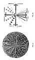
- FIG. 2Ashows a diagram on the left with a radial scanning system and in FIG. 2B an image on the right created by the scanning operation;
- FIG. 3Ashows an image created by scanning a wafer with a non-vibrating contact potential difference sensor
- FIG. 3Bis an image after thresholding where the dark regions in the thresholded image represent non-uniformities
- FIGS. 4A-4Cshow three different images where FIG. 4A was formed by integrating the signal in the image in FIG. 3A ;
- FIG. 4Bshows the image after applying a threshold to identify areas of increased surface potential;
- FIG. 4Cshows the image after thresholding to identify regions of decreased surface potential;
- FIGS. 5A-5Cshow three images, and the image of FIG. 5A was created by scanning a wafer with a non-vibrating contact potential difference sensor with no surface illumination; FIG. 5B was created by scanning the same wafer with the surface illuminated by visible light; and FIG. 5C is the difference between the images of FIG. 5A and FIG. 5B ;
- FIGS. 6A-6Cshow three images, and the image of FIG. 6A was acquired by scanning a wafer with a non-vibrating contact potential difference sensor with a 5 Volt bias applied to the probe tip; the image of FIG. 6B is an image of the same wafer with a ⁇ 5 Volt bias applied to the probe tip,and the image of FIG. 6C is the difference of the images of FIGS. 6A and 6B ;
- FIG. 7shows an image of a wafer acquired by scanning with a non-vibrating contact potential difference sensor
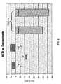
- FIG. 8shows Absolute CPD Measurements (ACMs) acquired with a vibrating Kelvin probe
- FIGS. 9A-9Dshow four images of the same wafer acquired by scanning the wafer with a non-vibrating contact potential difference sensor; the image of FIG. 9A is acquired with no bias voltage applied between the probe tip and the wafer surface; the image of FIG. 9B was acquired with a 5 Volt bias applied to the probe tip; and the image of FIG. 9C shows a height change feature of the wafer; and the image of FIG. 9D was formed by using the vibrating Kelvin probe mode to measure the contact potential difference between the probe tip and the wafer surface at multiple points, and then applying the negative of the average contact potential difference to the probe tip.
- the present inventionprovides an enhanced inspection system that uses a non-vibrating contact potential difference sensor system to detect surface and sub-surface non-uniformities, including deposited (or otherwise present) charge, and a system for processing data from the non-vibrating contact potential difference sensor to classify different types and relative amounts of non-uniformities.
- This inventionis not limited to the measurement of semiconductors with bare, clean surfaces. The chemical state of the surface may vary, or surface contamination may be present.
- the wafer surfacemay be covered with a coating or film. For example, a silicon wafer surface is often coated with a silicon oxide or other dielectric or metal film.
- This inventioncan be used to inspect a wafer covered with a film to detect defects in the underlying semiconductor or at the semiconductor-film interface. In addition, this invention can be used to detect or classify defects in, or on, a film.
- the apparatusconsists of a non-vibrating contact potential difference sensor 101 , a system 103 for mechanically fixturing the wafer 105 , a system 107 for positioning the sensor 101 a fixed distance above the wafer surface 106 and generating relative motion between the probe tip 102 and wafer surface 106 such that the sensor probe tip 102 moves parallel to the wafer surface 106 , a source of illumination 109 with variable intensity, angle, or spectrum of light that can irradiate the semiconductor wafer surface 106 under or near the sensor probe tip 102 , a source of charge 110 that can deposit a known amount of charge on the wafer surface 106 prior to scanning by the sensor probe tip 102 , a system 104 for vibrating the probe tip perpendicular to the wafer surface, and a system 112 for acquiring and processing the output signal from the sensor 101 to identify and classify wafer 105 non-uniformities.
- a semiconductor wafer 105is placed on a conductive wafer fixture 103 . This may be done manually or using an automated process such as, but not limited to, a wafer handling robot. The wafer 105 is held in place such as by using vacuum. Alternative methods of holding the wafer 105 include, but are not limited to, electrostatic forces and edge gripping.
- the fixture 103is mounted to a spindle which can rotate the wafer 105 about its center.
- the non-vibrating contact potential difference sensor 101is attached to a positioning system 107 that can adjust the height of the sensor 101 above the wafer surface 106 and can move the sensor 101 radially from at least the center of the wafer 105 to one edge of the wafer 105 .
- the non-vibrating contact potential difference sensor 101is electrically connected to the wafer surface 106 via the conductive wafer fixture 103 . This connection can be resistive or capacitive.
- a height sensor 111that has been calibrated to the height of the non-vibrating contact potential difference sensor probe tip 102 is also mounted on the same positioning system 107 as the non-vibrating contact potential difference sensor 101 .
- a light source 109 with variable intensity, wavelength or anglemay be mounted on the positioning system such that the illuminated area includes at least the area next to the non-vibrating contact potential difference sensor probe tip 102 .
- a light sourcecan be mounted separate from the positioning system so that it illuminates at least the entire area scanned by the non-vibrating contact potential difference sensor.
- a source of controlled chargemay be mounted on the positioning system so that a known amount of charge can be deposited on the wafer surface, or on or in a dielectric layer present on the wafer, prior to, or even during, scanning by the non-vibrating contact potential difference sensor.
- a system 104 for vibrating the sensor 101 perpendicular to the wafer surface 106is attached to the contact potential difference sensor. This system is used to make vibrating Kelvin probe measurements of the contact potential difference between the probe tip 102 and the wafer surface 106 .
- the height sensor 111is positioned above one or more points on the wafer surface 106 and the height of the wafer surface 106 is measured. These wafer height measurements are used to calculate the position of the non-vibrating contact potential difference sensor 101 that will produce the desired distance between the probe tip 102 and the wafer surface 106 . This information is used to position the probe tip 102 at a fixed height above the wafer surface 106 , and the probe tip 102 is moved to a point above the outside edge of the wafer 105 . Illumination of the wafer surface may be enabled and the appropriate intensity and wavelength selected for the inspection application. Also, the appropriate amount of charge may be selected for the inspection application.
- the probe 101is held stationary and the wafer 105 is rotated on the spindle such that the probe tip 102 moves relative to the wafer 105 along a circular path that is centered at the wafer 105 center.
- Datais acquired during a single rotation of the wafer 105 .
- the sensor 101is then moved a programmable distance along the radius of the wafer 105 towards the wafer center. Another rotation of data is acquired at this new radius.
- the probe tip 102continues to step and scan concentric circular regions of the wafer 105 until the probe reaches the wafer 105 center.
- the resulting datais then assembled into an image of the wafer 105 .
- each concentric circular region of the wafer 105could be scanned multiple times and the resulting data averaged to reduce the effect of random noise.
- This imageis processed to identify and classify non-uniformities (see FIG. 2B ).
- This processingcan take many forms. It may be as simple as the thresholding of signal values to detect regions of the wafer surface 106 where the surface potential is changing (compare FIGS. 3A and 3B ).
- the differential sensor datacan also be integrated to generate an image which represents relative surface potential values.
- This integrated imagecan also be processed or thresholded to identify regions with specific relative potential values.
- the integrated imagecan be calibrated using multiple vibrating Kelvin probe measurements to produce an image with values that represent the absolute contact potential difference value at each point on the wafer. This image can then be thresholded to identify regions with specific contact potential difference values.
- FIG. 2Ashow a diagram of the radial scanning of one embodiment of the present invention.
- the non-vibrating contact potential difference sensor probe tip 102is positioned at point “A” near the edge of the wafer 105 .
- the wafer 105is rotated on the wafer fixture 103 and a circular track of data is scanned.
- the probe tip 102is moved a programmable distance towards the wafer 105 center to point “B” and a second circular track of data is scanned. This process is repeated until the probe tip 102 reaches the center of the wafer 105 .
- the resulting datais combined into an image of the wafer surface 106 .
- a sample imageis shown in FIG. 2B , and the light and dark regions representing various non-uniformities.
- the differential non-vibrating contact potential difference sensor signalcan be integrated to form a signal that represents relative surface potential or capacitance values. As shown in FIGS. 3A and 3B , this integrated signal can be thresholded to identify regions with signal values that lie within a specific range, or are above or below specified values. As shown in FIGS.
- a non-uniformitycan be classified as having a positive or negative sign based on whether the integrated signal is higher or lower than the integrated signal values for the surrounding wafer surface, or it can be classified as positive or negative based on whether the integrated signal value is higher or lower than the average integrated signal value for some portion of the wafer surface.
- the integrated imageshows regions of relative surface potential. Some regions are bright indicating areas of FIG. 4A with increased surface potential or work function and some regions are dark indicating areas of decreased surface potential or work function. In this case the bright regions are metal patterns on the wafer and the dark regions are non-metal or organic contaminants on the wafer.
- FIG. 4Bis the image from FIG. 4A after applying a threshold to identify areas of increased surface potential.
- the dark regionsshow areas of the image which are greater than a positive threshold. These regions represent areas of increased surface potential or work function and correspond to the metal pattern.
- the image of FIG. 4Cis the image of FIG. 4A after thresholding to identify regions of decreased surface potential. Dark regions show areas of the image which are less than a negative threshold. These regions represent areas of decreased surface potential or work function, and correspond to regions of non-metallic contamination.
- the polarity of the non-uniformityindicates whether the wafer height at the non-uniformity is higher or lower than the surrounding area.
- the polarity of the non-uniformityindicates if the surface potential is higher or lower at the non-uniformity.
- This informationcan be used to classify different types of chemical non-uniformities. For example, contamination of a silicon surface with some types of metals will result in an increase in surface potential, while contamination with many organics will result in a decrease in surface potential. In this case it is possible to discriminate between metal and organic contaminants based on the direction of surface potential change. Independent data from other sensors of conventional nature can be readily used to infer likely types of non-uniformity. In addition, the basic nature of a manufacturing process will provide clues as to the category of non-uniformity.
- a second aspect of the inventionrelates to the discrimination and classification of non-uniformities as resulting from changes in capacitance between the probe tip and the wafer surface or resulting from changes in potential between the probe tip and the wafer surface (see, for example, FIGS. 9A-9D ).
- Features in the imageinclude both chemical non-uniformities and height changes.
- the highlighted feature in FIG. 9Bis surface contamination which causes a change in surface potential on the wafer.
- the feature highlighted in FIG. 9Cis a change in wafer height resulting from a particle trapped between the wafer and the vacuum chuck used to secure the wafer for scanning. The trapped particle causes a local increase in the height of the wafer surface, which results in a change in capacitance between the wafer surface and the probe tip.
- the signal resulting from the change in surface potential of FIG. 9Bis relatively unchanged from the image of FIG. 9A , but the signal from the change in capacitance is amplified by the bias voltage. This is illustrated by the details of the image of FIG. 9B , which is formed by subtracting the image of FIG. 9A from the image of FIG. 9B .
- the surface potential featureis removed from the image by the subtraction operation but the change in capacitance feature remains.
- This techniqueis used to detect and classify height non-uniformities on the wafer, or to discriminate height non-uniformities from surface potential non-uniformities.
- the resulting scan in FIG. 9Dclearly shows chemical non-uniformities, but height non-uniformities are largely eliminated. This technique is used to detect and classify non-uniformities resulting from changes is surface potential.
- the wafermay be scanned twice with different bias voltages and one image subtracted from the other to form a new image that minimizes the signal resulting from surface potential non-uniformities and increases the signal resulting from wafer height non-uniformities.
- Non-uniformities which are detected in the resulting imageare classified as height non-uniformities (see also FIGS. 6A-6C ).
- FIGS. 6A-6Cshow three images, and the image of FIG. 6A was acquired by scanning a wafer with a non-vibrating contact potential difference sensor with a 5 Volt bias applied to the probe tip.
- the non-uniformities in the upper right and lower left quadrants of the waferare etched trenches in the silicon.
- the signal from these featuresis generated by changes in the height of the wafer surface which induces a capacitance change between the sensor probe tip and the wafer.
- the non-uniformities in the lower right quadrantare a thin film of metal.
- the signal from these featuresis generated by a change in surface potential; the image of FIG. 6B is an image of the same wafer with a ⁇ 5 Volt bias applied to the probe tip,and the image of FIG. 6C is the difference of the images of FIGS. 6A and 6B .
- the etched trenchesare clearly visible; but the other features, which result from surface chemistry changes, are eliminated.
- a vibrating Kelvin probe measurement of the contact potential difference between the probe tip and the wafer surfacecan be made at one or more points on a wafer. This measurement can determine the average contact potential difference between the probe tip and the wafer surface; or the average contact potential difference of a particular type of wafer can be determined by measuring one or more wafers of that type.
- a bias voltage that is equal in magnitude but opposite in sign to this average contact potential differencecan be applied to subsequent scans to minimize the signal resulting from changes in capacitance between the probe tip and the wafer surface. Non-uniformities in the resulting image are classified as changes in wafer surface potential as opposed to changes in capacitance.
- a third aspect of this inventionis the identification or classification of non-uniformities based on shape or signal value statistics. After non-uniformities in or on the wafer have been identified from the non-vibrating contact potential difference image, or from an integrated version of the image, then these non-uniformities can be classified based on features extracted from the differential image, the integrated image or from an integrated image scaled to vibrating Kelvin probe measurements. These features can consist of values describing the shape of the non-uniformity; such as area, perimeter, height and width; or the signal values associated with the non-uniformity; such as standard deviation, maximum, minimum, range, and average. In addition, features describing the position of the non-uniformity on the wafer or the relative positions of non-uniformities can be used to classify non-uniformities.
- a fourth aspect of this inventionis the classification of non-uniformities based on the sensitivity of the non-uniformity to light or surface deposited charge.
- Some types of non-uniformitiessuch as doping or implant non-uniformities, or charging in or on a dielectric film on or in a semiconductor substrate, are sensitive to surface illumination or charging.
- Two imagescan be acquired with different surface illumination conditions and the images subtracted. The resulting image shows changes in surface potential with illumination (see FIGS. 5A-5C ).
- FIGS. 5A-5Cshow three images, and the image of FIG. 5A was created by scanning a wafer with a non-vibrating contact potential difference sensor with no surface illumination; FIG.
- a fifth aspect of this inventionis the classification of non-uniformities based on the results of subsequent vibrating contact potential difference measurements.
- the non-vibrating contact potential difference sensorproduces differential data that represents changes in surface potential or height across the wafer.
- Vibrating Kelvin probe measurementsprovide a measure of the absolute contact potential difference between the sensor probe tip and the wafer surface (see FIG. 8 ). Measurements were made on a silicon surface contaminated with both metallic and organic contaminants. The organic contaminants result in lower contact potential difference values than the metallic contaminants.
- each quadrant of FIG. 7were created by applying different metals to the surface of the wafer. Vibrating contact potential difference sensor measurements were then made at the locations of non-uniformities identified in each quadrant.
- the vibrating contact potential difference measurementsshow different surface potential values for each of the metals, illustrating how vibrating contact potential difference sensor measurements can be used to classify defects detected by the non-vibrating contact potential difference scanned image.
- the contact potential difference as measured by the vibrating Kelvin probeusually varies with surface chemistry and these measurements can provide information that is useful in classifying surface non-uniformities.
- some types of non-uniformitiessuch as charges (deposited or otherwise present) trapped in or on a dielectric deposited on the surface of the wafer, can create relatively large contact potential difference measurements. Charging non-uniformities that produce relatively large signals can be classified based on the magnitude of the measurement and also on changes of the level of signal. For example, a contact potential difference measurement of over one Volt is often due to charging in a dielectric.
- a sixth aspect of this inventionis the classification of non-uniformities based on contact potential difference values obtained by scaling integrated non-vibrating contact potential difference image to two or more vibrating contact potential difference measurements (see FIG. 7 ).
- the resulting image valuesrepresent approximate contact potential difference values at each point in the image. These values can be used much like vibrating contact potential difference measurements to classify non-uniformities based on absolute contact potential difference values.
- the resulting imageis useful for identifying regions with specific surface potential values, and is particularly useful for detecting and classifying areas of large contact potential difference that typically result from charging in or on a dielectric.
- the non-vibrating contact potential difference sensor 101 , height sensor 111 , illumination source 109 , charge source 110 , and system for vibrating the sensor 104could all be mounted at fixed locations, and the wafer 105 could be moved and rotated beneath these stationary elements.
- the non-vibrating contact potential difference sensor 101could be moved continuously along the wafer 105 radius while the wafer 105 is spinning to create a continuous stream of data that spirals across the whole surface of the wafer 105 .
- the non-vibrating contact potential difference sensor 101could be moved linearly across the wafer 105 in a back-and-forth manner to scan the entire wafer surface 106 .
- multiple non-vibrating contact potential difference sensors and illumination sourcescould be used to acquire multiple measurements simultaneously to reduce the time required to measure a wafer.
Landscapes
- Engineering & Computer Science (AREA)
- Health & Medical Sciences (AREA)
- General Health & Medical Sciences (AREA)
- General Physics & Mathematics (AREA)
- Manufacturing & Machinery (AREA)
- Physics & Mathematics (AREA)
- Chemical & Material Sciences (AREA)
- Radiology & Medical Imaging (AREA)
- Chemical Kinetics & Catalysis (AREA)
- Life Sciences & Earth Sciences (AREA)
- Analytical Chemistry (AREA)
- Biochemistry (AREA)
- Immunology (AREA)
- Pathology (AREA)
- Electrochemistry (AREA)
- Nuclear Medicine, Radiotherapy & Molecular Imaging (AREA)
- Computer Hardware Design (AREA)
- Microelectronics & Electronic Packaging (AREA)
- Power Engineering (AREA)
- Testing Or Measuring Of Semiconductors Or The Like (AREA)
- Investigating Or Analyzing Materials By The Use Of Electric Means (AREA)
Abstract
Description
Q=CV (1)
Claims (21)
Priority Applications (4)
| Application Number | Priority Date | Filing Date | Title |
|---|---|---|---|
| US11/948,518US7900526B2 (en) | 2007-11-30 | 2007-11-30 | Defect classification utilizing data from a non-vibrating contact potential difference sensor |
| EP08857056AEP2232544A4 (en) | 2007-11-30 | 2008-11-25 | Defect classification utilizing data from a non-vibrating contact potential difference sensor |
| PCT/US2008/084720WO2009073485A1 (en) | 2007-11-30 | 2008-11-25 | Defect classification utilizing data from a non-vibrating contact potential difference sensor |
| TW097145908ATWI430379B (en) | 2007-11-30 | 2008-11-27 | Defect classification utilizing data from a non-vibrating contact potential difference sensor |
Applications Claiming Priority (1)
| Application Number | Priority Date | Filing Date | Title |
|---|---|---|---|
| US11/948,518US7900526B2 (en) | 2007-11-30 | 2007-11-30 | Defect classification utilizing data from a non-vibrating contact potential difference sensor |
Publications (2)
| Publication Number | Publication Date |
|---|---|
| US20090139312A1 US20090139312A1 (en) | 2009-06-04 |
| US7900526B2true US7900526B2 (en) | 2011-03-08 |
Family
ID=40674396
Family Applications (1)
| Application Number | Title | Priority Date | Filing Date |
|---|---|---|---|
| US11/948,518Expired - Fee RelatedUS7900526B2 (en) | 2007-11-30 | 2007-11-30 | Defect classification utilizing data from a non-vibrating contact potential difference sensor |
Country Status (4)
| Country | Link |
|---|---|
| US (1) | US7900526B2 (en) |
| EP (1) | EP2232544A4 (en) |
| TW (1) | TWI430379B (en) |
| WO (1) | WO2009073485A1 (en) |
Cited By (2)
| Publication number | Priority date | Publication date | Assignee | Title |
|---|---|---|---|---|
| US9453801B2 (en) | 2012-05-25 | 2016-09-27 | Kla-Tencor Corporation | Photoemission monitoring of EUV mirror and mask surface contamination in actinic EUV systems |
| US20170266744A1 (en)* | 2015-10-30 | 2017-09-21 | Mitsubishi Electric Corporation | Wire electric discharge machine, control method of control device of wire electric discharge machine, and positioning method |
Families Citing this family (4)
| Publication number | Priority date | Publication date | Assignee | Title |
|---|---|---|---|---|
| US7107158B2 (en)* | 2003-02-03 | 2006-09-12 | Qcept Technologies, Inc. | Inspection system and apparatus |
| US7944550B2 (en)* | 2008-02-29 | 2011-05-17 | International Business Machines Corporation | System and method for detecting local mechanical stress in integreated devices |
| US10088413B2 (en) | 2011-11-21 | 2018-10-02 | Kla-Tencor Corporation | Spectral matching based calibration |
| US11055553B1 (en)* | 2020-04-20 | 2021-07-06 | Nanya Technology Corporation | Image processing system and method |
Citations (75)
| Publication number | Priority date | Publication date | Assignee | Title |
|---|---|---|---|---|
| US4166974A (en) | 1978-01-23 | 1979-09-04 | The United States Of America As Represented By The Secretary Of The Navy | Apparatus and method for measuring capacitive energy |
| US4295092A (en) | 1978-02-09 | 1981-10-13 | Koa Oil Company, Limited | Apparatus for and method of detecting and measuring corrosion damage in pipe |
| US4481616A (en) | 1981-09-30 | 1984-11-06 | Rca Corporation | Scanning capacitance microscope |
| US4767211A (en) | 1984-10-08 | 1988-08-30 | Hitachi, Ltd. | Apparatus for and method of measuring boundary surface |
| US4973910A (en) | 1988-01-14 | 1990-11-27 | Wilson Mahlon S | Surface potential analyzer |
| DD297509A5 (en) | 1990-03-13 | 1992-01-09 | Kloeden,Rolf,De | CAPACITIVE SENSOR FOR CONTACTLESS ROUGHNESS MEASUREMENT |
| US5087533A (en) | 1989-10-12 | 1992-02-11 | Brown Paul M | Contact potential difference cell |
| US5136247A (en) | 1991-01-18 | 1992-08-04 | Hansen Wilford N | Apparatus and methods for calibrated work function measurements |
| US5214389A (en) | 1992-01-06 | 1993-05-25 | Motorola, Inc. | Multi-dimensional high-resolution probe for semiconductor measurements including piezoelectric transducer arrangement for controlling probe position |
| US5218362A (en) | 1992-07-02 | 1993-06-08 | National Semiconductor Corporation | Multistep analog-to-digital converter with embedded correction data memory for trimming resistor ladders |
| US5217907A (en) | 1992-01-28 | 1993-06-08 | National Semiconductor Corporation | Array spreading resistance probe (ASRP) method for profile extraction from semiconductor chips of cellular construction |
| US5270664A (en) | 1990-10-03 | 1993-12-14 | Renishaw, Plc | Probe for measuring surface roughness by sensing fringe field capacitance effects |
| US5272443A (en) | 1992-04-22 | 1993-12-21 | Aluminum Company Of America | Chatter and profile measuring using capacitor sensors |
| US5278407A (en) | 1991-04-25 | 1994-01-11 | Hitachi, Ltd. | Secondary-ion mass spectrometry apparatus using field limiting method |
| US5293131A (en) | 1992-09-04 | 1994-03-08 | Measurement Systems, Inc. | Capacitive probe for bore measurement |
| US5315259A (en) | 1992-05-26 | 1994-05-24 | Universities Research Association, Inc. | Omnidirectional capacitive probe for gauge of having a sensing tip formed as a substantially complete sphere |
| US5369370A (en) | 1990-06-13 | 1994-11-29 | Max-Planck-Institut Fuer Eisenforschung Gmbh | Method and apparatus for the measurement of the corrosion potential between a coated metal surface and a reference electrode |
| US5381101A (en) | 1992-12-02 | 1995-01-10 | The Board Of Trustees Of The Leland Stanford Junior University | System and method of measuring high-speed electrical waveforms using force microscopy and offset sampling frequencies |
| US5460684A (en) | 1992-12-04 | 1995-10-24 | Tokyo Electron Limited | Stage having electrostatic chuck and plasma processing apparatus using same |
| US5517123A (en) | 1994-08-26 | 1996-05-14 | Analog Devices, Inc. | High sensitivity integrated micromechanical electrostatic potential sensor |
| US5546477A (en) | 1993-03-30 | 1996-08-13 | Klics, Inc. | Data compression and decompression |
| US5583443A (en) | 1990-10-03 | 1996-12-10 | Renishaw Plc | Calibration of capacitance probe |
| US5723980A (en) | 1995-06-07 | 1998-03-03 | Aerogage Corporation | Clearance measurement system |
| US5723981A (en) | 1994-08-29 | 1998-03-03 | Imec Vzw | Method for measuring the electrical potential in a semiconductor element |
| US5773989A (en) | 1995-07-14 | 1998-06-30 | University Of South Florida | Measurement of the mobile ion concentration in the oxide layer of a semiconductor wafer |
| US5789360A (en) | 1996-03-04 | 1998-08-04 | Samsung Electronics Co., Ltd. | Cleaning solution for use on a semiconductor wafer following chemical-mechanical polishing of the wafer and method for using same |
| US5977788A (en) | 1997-07-11 | 1999-11-02 | Lagowski; Jacek | Elevated temperature measurement of the minority carrier lifetime in the depletion layer of a semiconductor wafer |
| US5974869A (en) | 1996-11-14 | 1999-11-02 | Georgia Tech Research Corp. | Non-vibrating capacitance probe for wear monitoring |
| US6011404A (en) | 1997-07-03 | 2000-01-04 | Lucent Technologies Inc. | System and method for determining near--surface lifetimes and the tunneling field of a dielectric in a semiconductor |
| US6037797A (en) | 1997-07-11 | 2000-03-14 | Semiconductor Diagnostics, Inc. | Measurement of the interface trap charge in an oxide semiconductor layer interface |
| US6091248A (en) | 1994-08-29 | 2000-07-18 | Imec Vzw | Method for measuring the electrical potential in a semiconductor element |
| US6094971A (en) | 1997-09-24 | 2000-08-01 | Texas Instruments Incorporated | Scanning-probe microscope including non-optical means for detecting normal tip-sample interactions |
| US6097196A (en) | 1997-04-23 | 2000-08-01 | Verkuil; Roger L. | Non-contact tunnelling field measurement for a semiconductor oxide layer |
| US6104481A (en)* | 1997-11-11 | 2000-08-15 | Kabushiki Kaisha Topcon | Surface inspection apparatus |
| US6114865A (en) | 1999-04-21 | 2000-09-05 | Semiconductor Diagnostics, Inc. | Device for electrically contacting a floating semiconductor wafer having an insulating film |
| EP1039277A1 (en) | 1999-03-22 | 2000-09-27 | Meritor Heavy Vehicle Systems, LLC | Torsional vibration monitoring system |
| US6127289A (en) | 1997-09-05 | 2000-10-03 | Lucent Technologies, Inc. | Method for treating semiconductor wafers with corona charge and devices using corona charging |
| US6139759A (en) | 1997-07-08 | 2000-10-31 | International Business Machines Corporation | Method of manufacturing silicided silicon microtips for scanning probe microscopy |
| US6201401B1 (en) | 1994-08-29 | 2001-03-13 | Imec | Method for measuring the electrical potential in a semiconductor element |
| US6232134B1 (en) | 2000-01-24 | 2001-05-15 | Motorola Inc. | Method and apparatus for monitoring wafer characteristics and/or semiconductor processing consistency using wafer charge distribution measurements |
| US6255128B1 (en) | 1998-08-06 | 2001-07-03 | Lucent Technologies Inc. | Non-contact method for determining the presence of a contaminant in a semiconductor device |
| US6265890B1 (en) | 1999-08-26 | 2001-07-24 | Lucent Technologies Inc. | In-line non-contact depletion capacitance measurement method and apparatus |
| WO2001090730A2 (en) | 2000-05-24 | 2001-11-29 | Sensorchem International Corporation | Scanning kelvin microprobe system and process for analyzing a surface |
| WO2002079754A2 (en) | 2001-03-29 | 2002-10-10 | Georgia Tech Research Corporation | Contact potential difference sensor to monitor oil properties |
| US6517669B2 (en) | 1999-02-26 | 2003-02-11 | Micron Technology, Inc. | Apparatus and method of detecting endpoint of a dielectric etch |
| US6520839B1 (en) | 1997-09-10 | 2003-02-18 | Speedfam-Ipec Corporation | Load and unload station for semiconductor wafers |
| US6538462B1 (en) | 1999-11-30 | 2003-03-25 | Semiconductor Diagnostics, Inc. | Method for measuring stress induced leakage current and gate dielectric integrity using corona discharge |
| US6546814B1 (en) | 1999-03-13 | 2003-04-15 | Textron Systems Corporation | Method and apparatus for estimating torque in rotating machinery |
| US6551972B1 (en) | 1997-07-10 | 2003-04-22 | Merck Patent Gesellschaft | Solutions for cleaning silicon semiconductors or silicon oxides |
| WO2003033993A1 (en) | 2001-10-19 | 2003-04-24 | Commonwealth Scientific And Industrial Research Organisation | A kelvin probe instrument |
| US6597193B2 (en) | 2001-01-26 | 2003-07-22 | Semiconductor Diagnostics, Inc. | Steady state method for measuring the thickness and the capacitance of ultra thin dielectric in the presence of substantial leakage current |
| US20030139838A1 (en) | 2002-01-16 | 2003-07-24 | Marella Paul Frank | Systems and methods for closed loop defect reduction |
| US20030164942A1 (en) | 1999-12-07 | 2003-09-04 | Kunihiko Take | Semiconductor wafer examination system |
| US20030175945A1 (en) | 2000-05-24 | 2003-09-18 | Michael Thompson | Scanning kelvin microprobe system and process for analyzing a surface |
| US6664800B2 (en) | 2001-01-08 | 2003-12-16 | Agere Systems Inc. | Non-contact method for determining quality of semiconductor dielectrics |
| US6664546B1 (en) | 2000-02-10 | 2003-12-16 | Kla-Tencor | In-situ probe for optimizing electron beam inspection and metrology based on surface potential |
| US6680621B2 (en) | 2001-01-26 | 2004-01-20 | Semiconductor Diagnostics, Inc. | Steady state method for measuring the thickness and the capacitance of ultra thin dielectric in the presence of substantial leakage current |
| US6679117B2 (en) | 2001-02-07 | 2004-01-20 | Georgia Tech Research Corporation | Ionization contact potential difference gyroscope |
| US20040058620A1 (en) | 2002-09-19 | 2004-03-25 | Lam Research Corporation | System and method for metal residue detection and mapping within a multi-step sequence |
| US20040057497A1 (en) | 2002-09-24 | 2004-03-25 | Lagowski Jacek J. | Method and system for elevated temperature measurement with probes designed for room temperature measurement |
| US6711952B2 (en) | 2001-10-05 | 2004-03-30 | General Electric Company | Method and system for monitoring bearings |
| US6717413B1 (en) | 2000-04-21 | 2004-04-06 | Georgia Tech Research Corporation | Contact potential difference ionization detector |
| US20040070355A1 (en) | 2002-10-09 | 2004-04-15 | Hibiki Ogura | Rotation speed control apparatus of open close body for vehicle and rotation speed control method of the same |
| US20040079142A1 (en)* | 2001-03-09 | 2004-04-29 | Roger Proksch | Apparatus and method for isolating and measuring movement in metrology apparatus |
| US20040105093A1 (en) | 2002-11-29 | 2004-06-03 | Akira Hamamatsu | Inspection method and inspection apparatus |
| US20040134515A1 (en) | 1999-10-29 | 2004-07-15 | Castrucci Paul P. | Apparatus and method for semiconductor wafer cleaning |
| US20040152250A1 (en) | 2003-02-03 | 2004-08-05 | Qcept Technologies | Semiconductor wafer inspection system |
| US6791310B2 (en) | 1999-03-15 | 2004-09-14 | Therma-Wave, Inc. | Systems and methods for improved metrology using combined optical and electrical measurements |
| US6803241B2 (en) | 2002-01-10 | 2004-10-12 | Samsung Electronics Co., Ltd. | Method of monitoring contact hole of integrated circuit using corona charges |
| US20040241890A1 (en) | 2003-02-03 | 2004-12-02 | Qcept Technologies, Inc. | Wafer inspection system |
| US20050016279A1 (en) | 2003-07-25 | 2005-01-27 | Qcept Technologies, Inc. | Measurement of motions of rotating shafts using non-vibrating contact potential difference sensor |
| US6849505B2 (en) | 2001-09-14 | 2005-02-01 | Hynix Semiconductor Inc. | Semiconductor device and method for fabricating the same |
| US20050162178A1 (en) | 2003-02-03 | 2005-07-28 | Qcept Technologies, Inc. | Inspection system and apparatus |
| US7385686B2 (en)* | 2003-06-27 | 2008-06-10 | Canon Kabushiki Kaisha | Method and apparatus for inspecting semiconductor device |
| US7420669B2 (en)* | 2004-07-01 | 2008-09-02 | Midwest Research Institute | Optic probe for semiconductor characterization |
Family Cites Families (1)
| Publication number | Priority date | Publication date | Assignee | Title |
|---|---|---|---|---|
| US6714831B2 (en)* | 2002-01-24 | 2004-03-30 | Ford Motor Company | Paint defect automated seek and repair assembly and method |
- 2007
- 2007-11-30USUS11/948,518patent/US7900526B2/ennot_activeExpired - Fee Related
- 2008
- 2008-11-25EPEP08857056Apatent/EP2232544A4/ennot_activeWithdrawn
- 2008-11-25WOPCT/US2008/084720patent/WO2009073485A1/enactiveApplication Filing
- 2008-11-27TWTW097145908Apatent/TWI430379B/ennot_activeIP Right Cessation
Patent Citations (87)
| Publication number | Priority date | Publication date | Assignee | Title |
|---|---|---|---|---|
| US4166974A (en) | 1978-01-23 | 1979-09-04 | The United States Of America As Represented By The Secretary Of The Navy | Apparatus and method for measuring capacitive energy |
| US4295092A (en) | 1978-02-09 | 1981-10-13 | Koa Oil Company, Limited | Apparatus for and method of detecting and measuring corrosion damage in pipe |
| US4481616A (en) | 1981-09-30 | 1984-11-06 | Rca Corporation | Scanning capacitance microscope |
| US4767211A (en) | 1984-10-08 | 1988-08-30 | Hitachi, Ltd. | Apparatus for and method of measuring boundary surface |
| US4973910A (en) | 1988-01-14 | 1990-11-27 | Wilson Mahlon S | Surface potential analyzer |
| US5087533A (en) | 1989-10-12 | 1992-02-11 | Brown Paul M | Contact potential difference cell |
| DD297509A5 (en) | 1990-03-13 | 1992-01-09 | Kloeden,Rolf,De | CAPACITIVE SENSOR FOR CONTACTLESS ROUGHNESS MEASUREMENT |
| US5369370A (en) | 1990-06-13 | 1994-11-29 | Max-Planck-Institut Fuer Eisenforschung Gmbh | Method and apparatus for the measurement of the corrosion potential between a coated metal surface and a reference electrode |
| US5270664A (en) | 1990-10-03 | 1993-12-14 | Renishaw, Plc | Probe for measuring surface roughness by sensing fringe field capacitance effects |
| US5583443A (en) | 1990-10-03 | 1996-12-10 | Renishaw Plc | Calibration of capacitance probe |
| US5136247A (en) | 1991-01-18 | 1992-08-04 | Hansen Wilford N | Apparatus and methods for calibrated work function measurements |
| US5278407A (en) | 1991-04-25 | 1994-01-11 | Hitachi, Ltd. | Secondary-ion mass spectrometry apparatus using field limiting method |
| US5214389A (en) | 1992-01-06 | 1993-05-25 | Motorola, Inc. | Multi-dimensional high-resolution probe for semiconductor measurements including piezoelectric transducer arrangement for controlling probe position |
| US5217907A (en) | 1992-01-28 | 1993-06-08 | National Semiconductor Corporation | Array spreading resistance probe (ASRP) method for profile extraction from semiconductor chips of cellular construction |
| US5272443A (en) | 1992-04-22 | 1993-12-21 | Aluminum Company Of America | Chatter and profile measuring using capacitor sensors |
| US5315259A (en) | 1992-05-26 | 1994-05-24 | Universities Research Association, Inc. | Omnidirectional capacitive probe for gauge of having a sensing tip formed as a substantially complete sphere |
| US5218362A (en) | 1992-07-02 | 1993-06-08 | National Semiconductor Corporation | Multistep analog-to-digital converter with embedded correction data memory for trimming resistor ladders |
| US5293131A (en) | 1992-09-04 | 1994-03-08 | Measurement Systems, Inc. | Capacitive probe for bore measurement |
| US5381101A (en) | 1992-12-02 | 1995-01-10 | The Board Of Trustees Of The Leland Stanford Junior University | System and method of measuring high-speed electrical waveforms using force microscopy and offset sampling frequencies |
| US5460684A (en) | 1992-12-04 | 1995-10-24 | Tokyo Electron Limited | Stage having electrostatic chuck and plasma processing apparatus using same |
| US5546477A (en) | 1993-03-30 | 1996-08-13 | Klics, Inc. | Data compression and decompression |
| US5517123A (en) | 1994-08-26 | 1996-05-14 | Analog Devices, Inc. | High sensitivity integrated micromechanical electrostatic potential sensor |
| US6091248A (en) | 1994-08-29 | 2000-07-18 | Imec Vzw | Method for measuring the electrical potential in a semiconductor element |
| US5723981A (en) | 1994-08-29 | 1998-03-03 | Imec Vzw | Method for measuring the electrical potential in a semiconductor element |
| US6201401B1 (en) | 1994-08-29 | 2001-03-13 | Imec | Method for measuring the electrical potential in a semiconductor element |
| US5723980A (en) | 1995-06-07 | 1998-03-03 | Aerogage Corporation | Clearance measurement system |
| US5773989A (en) | 1995-07-14 | 1998-06-30 | University Of South Florida | Measurement of the mobile ion concentration in the oxide layer of a semiconductor wafer |
| US5789360A (en) | 1996-03-04 | 1998-08-04 | Samsung Electronics Co., Ltd. | Cleaning solution for use on a semiconductor wafer following chemical-mechanical polishing of the wafer and method for using same |
| US5974869A (en) | 1996-11-14 | 1999-11-02 | Georgia Tech Research Corp. | Non-vibrating capacitance probe for wear monitoring |
| USRE39803E1 (en) | 1996-11-14 | 2007-09-04 | Georgia Tech Research Corporation | Non vibrating capacitance probe for wear monitoring |
| US6097196A (en) | 1997-04-23 | 2000-08-01 | Verkuil; Roger L. | Non-contact tunnelling field measurement for a semiconductor oxide layer |
| US6011404A (en) | 1997-07-03 | 2000-01-04 | Lucent Technologies Inc. | System and method for determining near--surface lifetimes and the tunneling field of a dielectric in a semiconductor |
| US6139759A (en) | 1997-07-08 | 2000-10-31 | International Business Machines Corporation | Method of manufacturing silicided silicon microtips for scanning probe microscopy |
| US6198300B1 (en) | 1997-07-08 | 2001-03-06 | International Business Machines Corporation | Silicided silicon microtips for scanning probe microscopy |
| US6551972B1 (en) | 1997-07-10 | 2003-04-22 | Merck Patent Gesellschaft | Solutions for cleaning silicon semiconductors or silicon oxides |
| US5977788A (en) | 1997-07-11 | 1999-11-02 | Lagowski; Jacek | Elevated temperature measurement of the minority carrier lifetime in the depletion layer of a semiconductor wafer |
| US6037797A (en) | 1997-07-11 | 2000-03-14 | Semiconductor Diagnostics, Inc. | Measurement of the interface trap charge in an oxide semiconductor layer interface |
| US6127289A (en) | 1997-09-05 | 2000-10-03 | Lucent Technologies, Inc. | Method for treating semiconductor wafers with corona charge and devices using corona charging |
| US6520839B1 (en) | 1997-09-10 | 2003-02-18 | Speedfam-Ipec Corporation | Load and unload station for semiconductor wafers |
| US6094971A (en) | 1997-09-24 | 2000-08-01 | Texas Instruments Incorporated | Scanning-probe microscope including non-optical means for detecting normal tip-sample interactions |
| US6104481A (en)* | 1997-11-11 | 2000-08-15 | Kabushiki Kaisha Topcon | Surface inspection apparatus |
| US6255128B1 (en) | 1998-08-06 | 2001-07-03 | Lucent Technologies Inc. | Non-contact method for determining the presence of a contaminant in a semiconductor device |
| US6517669B2 (en) | 1999-02-26 | 2003-02-11 | Micron Technology, Inc. | Apparatus and method of detecting endpoint of a dielectric etch |
| US6546814B1 (en) | 1999-03-13 | 2003-04-15 | Textron Systems Corporation | Method and apparatus for estimating torque in rotating machinery |
| US6791310B2 (en) | 1999-03-15 | 2004-09-14 | Therma-Wave, Inc. | Systems and methods for improved metrology using combined optical and electrical measurements |
| EP1039277A1 (en) | 1999-03-22 | 2000-09-27 | Meritor Heavy Vehicle Systems, LLC | Torsional vibration monitoring system |
| US6114865A (en) | 1999-04-21 | 2000-09-05 | Semiconductor Diagnostics, Inc. | Device for electrically contacting a floating semiconductor wafer having an insulating film |
| US6265890B1 (en) | 1999-08-26 | 2001-07-24 | Lucent Technologies Inc. | In-line non-contact depletion capacitance measurement method and apparatus |
| US20040134515A1 (en) | 1999-10-29 | 2004-07-15 | Castrucci Paul P. | Apparatus and method for semiconductor wafer cleaning |
| US6858089B2 (en) | 1999-10-29 | 2005-02-22 | Paul P. Castrucci | Apparatus and method for semiconductor wafer cleaning |
| US6538462B1 (en) | 1999-11-30 | 2003-03-25 | Semiconductor Diagnostics, Inc. | Method for measuring stress induced leakage current and gate dielectric integrity using corona discharge |
| US20030164942A1 (en) | 1999-12-07 | 2003-09-04 | Kunihiko Take | Semiconductor wafer examination system |
| US6232134B1 (en) | 2000-01-24 | 2001-05-15 | Motorola Inc. | Method and apparatus for monitoring wafer characteristics and/or semiconductor processing consistency using wafer charge distribution measurements |
| US6664546B1 (en) | 2000-02-10 | 2003-12-16 | Kla-Tencor | In-situ probe for optimizing electron beam inspection and metrology based on surface potential |
| US6717413B1 (en) | 2000-04-21 | 2004-04-06 | Georgia Tech Research Corporation | Contact potential difference ionization detector |
| US7084661B2 (en) | 2000-05-24 | 2006-08-01 | Sensorchem International Corporation | Scanning kelvin microprobe system and process for analyzing a surface |
| US20040029131A1 (en) | 2000-05-24 | 2004-02-12 | Michael Thompson | Scanning kelvinmicroprobe system and process for biomolecule microassay |
| US20030175945A1 (en) | 2000-05-24 | 2003-09-18 | Michael Thompson | Scanning kelvin microprobe system and process for analyzing a surface |
| WO2001090730A2 (en) | 2000-05-24 | 2001-11-29 | Sensorchem International Corporation | Scanning kelvin microprobe system and process for analyzing a surface |
| US6664800B2 (en) | 2001-01-08 | 2003-12-16 | Agere Systems Inc. | Non-contact method for determining quality of semiconductor dielectrics |
| US6680621B2 (en) | 2001-01-26 | 2004-01-20 | Semiconductor Diagnostics, Inc. | Steady state method for measuring the thickness and the capacitance of ultra thin dielectric in the presence of substantial leakage current |
| US6597193B2 (en) | 2001-01-26 | 2003-07-22 | Semiconductor Diagnostics, Inc. | Steady state method for measuring the thickness and the capacitance of ultra thin dielectric in the presence of substantial leakage current |
| US6679117B2 (en) | 2001-02-07 | 2004-01-20 | Georgia Tech Research Corporation | Ionization contact potential difference gyroscope |
| US20040079142A1 (en)* | 2001-03-09 | 2004-04-29 | Roger Proksch | Apparatus and method for isolating and measuring movement in metrology apparatus |
| US7019654B2 (en) | 2001-03-29 | 2006-03-28 | Georgia Tech Research Corporation | Contact potential difference sensor to monitor oil properties |
| WO2002079754A2 (en) | 2001-03-29 | 2002-10-10 | Georgia Tech Research Corporation | Contact potential difference sensor to monitor oil properties |
| US6849505B2 (en) | 2001-09-14 | 2005-02-01 | Hynix Semiconductor Inc. | Semiconductor device and method for fabricating the same |
| EP1304463B1 (en) | 2001-10-05 | 2005-09-14 | General Electric Company | Method and system for monitoring bearings |
| US6711952B2 (en) | 2001-10-05 | 2004-03-30 | General Electric Company | Method and system for monitoring bearings |
| WO2003033993A1 (en) | 2001-10-19 | 2003-04-24 | Commonwealth Scientific And Industrial Research Organisation | A kelvin probe instrument |
| US6803241B2 (en) | 2002-01-10 | 2004-10-12 | Samsung Electronics Co., Ltd. | Method of monitoring contact hole of integrated circuit using corona charges |
| US20030139838A1 (en) | 2002-01-16 | 2003-07-24 | Marella Paul Frank | Systems and methods for closed loop defect reduction |
| US6929531B2 (en) | 2002-09-19 | 2005-08-16 | Lam Research Corporation | System and method for metal residue detection and mapping within a multi-step sequence |
| US20040058620A1 (en) | 2002-09-19 | 2004-03-25 | Lam Research Corporation | System and method for metal residue detection and mapping within a multi-step sequence |
| US6771091B2 (en) | 2002-09-24 | 2004-08-03 | Semiconductor Diagnostics, Inc. | Method and system for elevated temperature measurement with probes designed for room temperature measurement |
| US20040057497A1 (en) | 2002-09-24 | 2004-03-25 | Lagowski Jacek J. | Method and system for elevated temperature measurement with probes designed for room temperature measurement |
| US20040070355A1 (en) | 2002-10-09 | 2004-04-15 | Hibiki Ogura | Rotation speed control apparatus of open close body for vehicle and rotation speed control method of the same |
| US20040105093A1 (en) | 2002-11-29 | 2004-06-03 | Akira Hamamatsu | Inspection method and inspection apparatus |
| US20050162178A1 (en) | 2003-02-03 | 2005-07-28 | Qcept Technologies, Inc. | Inspection system and apparatus |
| US20040241890A1 (en) | 2003-02-03 | 2004-12-02 | Qcept Technologies, Inc. | Wafer inspection system |
| WO2004070355A2 (en) | 2003-02-03 | 2004-08-19 | Qcept Technologies Inc. | Wafer inspection using a nonvibrating contact potential difference probe (nonvibrating kelvin probe) |
| US7107158B2 (en) | 2003-02-03 | 2006-09-12 | Qcept Technologies, Inc. | Inspection system and apparatus |
| US20070010954A1 (en) | 2003-02-03 | 2007-01-11 | Qcept Technologies, Inc. | Inspection system and apparatus |
| US20040152250A1 (en) | 2003-02-03 | 2004-08-05 | Qcept Technologies | Semiconductor wafer inspection system |
| US7385686B2 (en)* | 2003-06-27 | 2008-06-10 | Canon Kabushiki Kaisha | Method and apparatus for inspecting semiconductor device |
| US20050016279A1 (en) | 2003-07-25 | 2005-01-27 | Qcept Technologies, Inc. | Measurement of motions of rotating shafts using non-vibrating contact potential difference sensor |
| US7420669B2 (en)* | 2004-07-01 | 2008-09-02 | Midwest Research Institute | Optic probe for semiconductor characterization |
Non-Patent Citations (6)
| Title |
|---|
| B Scruton and B.H. Blott, A High Resolution Probe for Scanning Electrostatic Potential Profiles Across Surfaces; Journal of Physics E: Scientific Instruments (May 1973), pp. 472-474; vol. 6, No. 5, Printed in Great Britain. |
| Castaldini A et al: "Scanning Kelvin probe and surface photovoltage analysis of multicrystalline silicon", Materials Science and Engineering B., Elsevier Sequoia, Lausanne, Ch; vol. 91-92, Apr. 30, 2002, pp. 234-238, XP004355534, ISSN: 0921-5107 (chapters 2.2 Scanning Kelvin probe: and "4.2 Scanning Kelvin probe analyses"). |
| Castaldini A et al: "Surface analyses of polycrystalline and Cz-Si wafers", Solar Energy Materials and Solar Cells, Elsevier Science Publishers, Amsterdam, NL; vol. 72, No. 1-4, Apr. 2002, pp. 425-432, XP004339790, ISSN: 0927-0248 (whole document). |
| Korach C S et al: "Measurement of perfluoropolyether lubricant thickness on a magnetic disk surface", Applied Physics Letters, American Institute of Physics, New York, NY, US; vol. 79, No. 5, Jul. 30, 2001, pp. 698-700, XP012029958, ISSN: 0003-6951 (p. 699, left column; fig. 2). |
| Yang Y et al: "Kelvin probe study on the perfluoropolyether film on metals", Tribology Letters, 2001, Kluwer Academic/Plenum Publishers, USA, vol. 10, No. 4, pp. 211-216, XP009035197, ISSN: 1023-8883 (p. 211-p. 212). |
| Yano D et al: "Nonvibrating contact potential difference probe measurement of a nanometer-scale lubricant on a hard disk", Journal of Tribology, American Society of Mechanical Engineers, New York, NY, US; vol. 121, No. 4, Oct. 1999, pp. 980-983, XP008031092, ISSN: 0742-4787 (pp. 980-981, fig. 4, first ref. on p. 983). |
Cited By (2)
| Publication number | Priority date | Publication date | Assignee | Title |
|---|---|---|---|---|
| US9453801B2 (en) | 2012-05-25 | 2016-09-27 | Kla-Tencor Corporation | Photoemission monitoring of EUV mirror and mask surface contamination in actinic EUV systems |
| US20170266744A1 (en)* | 2015-10-30 | 2017-09-21 | Mitsubishi Electric Corporation | Wire electric discharge machine, control method of control device of wire electric discharge machine, and positioning method |
Also Published As
| Publication number | Publication date |
|---|---|
| EP2232544A1 (en) | 2010-09-29 |
| EP2232544A4 (en) | 2013-01-30 |
| WO2009073485A1 (en) | 2009-06-11 |
| TW200935538A (en) | 2009-08-16 |
| TWI430379B (en) | 2014-03-11 |
| US20090139312A1 (en) | 2009-06-04 |
Similar Documents
| Publication | Publication Date | Title |
|---|---|---|
| US7634365B2 (en) | Inspection system and apparatus | |
| US7308367B2 (en) | Wafer inspection system | |
| KR100929768B1 (en) | Semiconductor inspection system and apparatus using non-vibration contact potential difference sensor and controlled illumination | |
| US7092826B2 (en) | Semiconductor wafer inspection system | |
| US7900526B2 (en) | Defect classification utilizing data from a non-vibrating contact potential difference sensor | |
| EP2274772B1 (en) | Calibration of non-vibrating contact potential difference measurements to detect surface variations that are perpendicular to the direction of sensor motion | |
| EP2394294B1 (en) | Patterned wafer inspection system using a non-vibrating contact potential difference sensor | |
| US7103482B2 (en) | Inspection system and apparatus |
Legal Events
| Date | Code | Title | Description |
|---|---|---|---|
| AS | Assignment | Owner name:QCEPT TECHNOLOGIES, INC., GEORGIA Free format text:ASSIGNMENT OF ASSIGNORS INTEREST;ASSIGNORS:HAWTHORNE, JEFFREY ALAN;STEELE, M. BRANDON;YANG, YEYUAN;AND OTHERS;REEL/FRAME:020183/0152 Effective date:20071129 | |
| FEPP | Fee payment procedure | Free format text:PAYOR NUMBER ASSIGNED (ORIGINAL EVENT CODE: ASPN); ENTITY STATUS OF PATENT OWNER: SMALL ENTITY | |
| STCF | Information on status: patent grant | Free format text:PATENTED CASE | |
| AS | Assignment | Owner name:RBC BANK (USA), NORTH CAROLINA Free format text:SECURITY AGREEMENT;ASSIGNOR:QCEPT TECHNOLOGIES INC.;REEL/FRAME:027919/0635 Effective date:20120301 | |
| AS | Assignment | Owner name:QCEPT TECHNOLOGIES INC., GEORGIA Free format text:SECURITY AGREEMENT;ASSIGNOR:PNC BANK FORMERLY RBC BANK;REEL/FRAME:032164/0589 Effective date:20140131 | |
| FPAY | Fee payment | Year of fee payment:4 | |
| AS | Assignment | Owner name:QCEPT INVESTMENTS LLC, GEORGIA Free format text:ASSIGNMENT OF ASSIGNORS INTEREST;ASSIGNOR:QCEPT TECHNOLOGIES INC.;REEL/FRAME:039151/0780 Effective date:20160609 | |
| AS | Assignment | Owner name:QCEPT TECHNOLOGIES INC, GEORGIA Free format text:RELEASE BY SECURED PARTY;ASSIGNOR:PNC BANK NATIONAL ASSOCIATION SUCCESSOR TO RBC BANK (USA);REEL/FRAME:039331/0211 Effective date:20160802 | |
| FEPP | Fee payment procedure | Free format text:MAINTENANCE FEE REMINDER MAILED (ORIGINAL EVENT CODE: REM.); ENTITY STATUS OF PATENT OWNER: SMALL ENTITY | |
| LAPS | Lapse for failure to pay maintenance fees | Free format text:PATENT EXPIRED FOR FAILURE TO PAY MAINTENANCE FEES (ORIGINAL EVENT CODE: EXP.); ENTITY STATUS OF PATENT OWNER: SMALL ENTITY | |
| STCH | Information on status: patent discontinuation | Free format text:PATENT EXPIRED DUE TO NONPAYMENT OF MAINTENANCE FEES UNDER 37 CFR 1.362 | |
| FP | Lapsed due to failure to pay maintenance fee | Effective date:20190308 |