US7898855B2 - Systems and methods for reducing unauthorized data recovery from solid-state storage devices - Google Patents
Systems and methods for reducing unauthorized data recovery from solid-state storage devicesDownload PDFInfo
- Publication number
- US7898855B2 US7898855B2US12/399,654US39965409AUS7898855B2US 7898855 B2US7898855 B2US 7898855B2US 39965409 AUS39965409 AUS 39965409AUS 7898855 B2US7898855 B2US 7898855B2
- Authority
- US
- United States
- Prior art keywords
- command
- memory
- data
- solid
- commands
- Prior art date
- Legal status (The legal status is an assumption and is not a legal conclusion. Google has not performed a legal analysis and makes no representation as to the accuracy of the status listed.)
- Expired - Lifetime
Links
Images


Classifications
- G—PHYSICS
- G06—COMPUTING OR CALCULATING; COUNTING
- G06F—ELECTRIC DIGITAL DATA PROCESSING
- G06F12/00—Accessing, addressing or allocating within memory systems or architectures
- G06F12/14—Protection against unauthorised use of memory or access to memory
- G06F12/1416—Protection against unauthorised use of memory or access to memory by checking the object accessibility, e.g. type of access defined by the memory independently of subject rights
- G06F12/1425—Protection against unauthorised use of memory or access to memory by checking the object accessibility, e.g. type of access defined by the memory independently of subject rights the protection being physical, e.g. cell, word, block
- G06F12/1433—Protection against unauthorised use of memory or access to memory by checking the object accessibility, e.g. type of access defined by the memory independently of subject rights the protection being physical, e.g. cell, word, block for a module or a part of a module
- G—PHYSICS
- G06—COMPUTING OR CALCULATING; COUNTING
- G06F—ELECTRIC DIGITAL DATA PROCESSING
- G06F21/00—Security arrangements for protecting computers, components thereof, programs or data against unauthorised activity
- G06F21/70—Protecting specific internal or peripheral components, in which the protection of a component leads to protection of the entire computer
- G06F21/78—Protecting specific internal or peripheral components, in which the protection of a component leads to protection of the entire computer to assure secure storage of data
- G06F21/79—Protecting specific internal or peripheral components, in which the protection of a component leads to protection of the entire computer to assure secure storage of data in semiconductor storage media, e.g. directly-addressable memories
- G—PHYSICS
- G11—INFORMATION STORAGE
- G11C—STATIC STORES
- G11C16/00—Erasable programmable read-only memories
- G11C16/02—Erasable programmable read-only memories electrically programmable
- G11C16/06—Auxiliary circuits, e.g. for writing into memory
- G11C16/22—Safety or protection circuits preventing unauthorised or accidental access to memory cells
- G—PHYSICS
- G06—COMPUTING OR CALCULATING; COUNTING
- G06F—ELECTRIC DIGITAL DATA PROCESSING
- G06F2221/00—Indexing scheme relating to security arrangements for protecting computers, components thereof, programs or data against unauthorised activity
- G06F2221/21—Indexing scheme relating to G06F21/00 and subgroups addressing additional information or applications relating to security arrangements for protecting computers, components thereof, programs or data against unauthorised activity
- G06F2221/2143—Clearing memory, e.g. to prevent the data from being stolen
- Y—GENERAL TAGGING OF NEW TECHNOLOGICAL DEVELOPMENTS; GENERAL TAGGING OF CROSS-SECTIONAL TECHNOLOGIES SPANNING OVER SEVERAL SECTIONS OF THE IPC; TECHNICAL SUBJECTS COVERED BY FORMER USPC CROSS-REFERENCE ART COLLECTIONS [XRACs] AND DIGESTS
- Y04—INFORMATION OR COMMUNICATION TECHNOLOGIES HAVING AN IMPACT ON OTHER TECHNOLOGY AREAS
- Y04S—SYSTEMS INTEGRATING TECHNOLOGIES RELATED TO POWER NETWORK OPERATION, COMMUNICATION OR INFORMATION TECHNOLOGIES FOR IMPROVING THE ELECTRICAL POWER GENERATION, TRANSMISSION, DISTRIBUTION, MANAGEMENT OR USAGE, i.e. SMART GRIDS
- Y04S40/00—Systems for electrical power generation, transmission, distribution or end-user application management characterised by the use of communication or information technologies, or communication or information technology specific aspects supporting them
- Y04S40/20—Information technology specific aspects, e.g. CAD, simulation, modelling, system security
Definitions
- the present inventionrelates to solid-state storage devices. More specifically, the present invention relates to electrically erasing and/or physically damaging solid-state storage devices.
- Solid-state storage solutionsare used to store a wide variety of data including sensitive information not intended for unauthorized users.
- a host computer systemmay store a person's personal or financial information on a solid-state memory device such as an advanced technology attachment (ATA) flash disk or a removable flash memory card.
- ATAadvanced technology attachment
- Solid-state storage solutionsalso store sensitive information including, for example, trade secrets, security information, military information, credit card information, or other information that a user desires to keep confidential.
- One approach to reducing unauthorized access to data stored on a solid-state memory deviceis to electrically erase a memory array within the memory device.
- Conventional systemsuse industry standard command sets such as those provided by ATA, CompactFlash (CF) card or PC card (also know as a PCMCIA card) standards to erase memory arrays.
- CFCompactFlash
- PC cardalso know as a PCMCIA card
- a hostsends standard read, erase and write commands to the memory device several times to ensure that the memory array is erased.
- Some systemsalso send additional commands to write a data pattern to the memory array to meet industry standard data sanitation specifications.
- Such erase and sanitation proceduresare cumbersome and generally require the host to repeatedly handshake with the memory device. Further, the host system will generally erase and sanitize multiple memory chips in a memory device sequentially with handshaking operations between erase operations. Thus, it can take several minutes or hours to complete an erase and sanitation procedure. In some applications such as avionics or power sensitive systems, sufficient time and/or power may not be available to adequately erase and sanitize the memory device. For example, it may not be possible to erase and sanitize the memory array during intermittent system power failures.
- Solid-state memory arraystypically comprise a semiconductor material such as silicon or the like. Even when the memory array is erased, it may still be possible to retrieve data by examining the semiconductor material for the effects of hysteresis. In military or other security sensitive applications, such data retrieval is generally unacceptable. Thus, the memory array is typically physically destroyed using, for example, one or more instruments to gain access to and destroy the memory array. However, there is not always enough time to physically locate and destroy the memory array. For example, a pilot forced to land a military aircraft in enemy territory may have very little time to electrically erase or physically destroy sensitive information in the memory array.
- a memory systemcomprising one or more memory devices is purged to prevent unauthorized access to data stored therein.
- a host systempasses control of purge operations to the memory system.
- the memory systemcan perform a purge operation on two or more memory devices in parallel.
- the memory systemincludes a destroy circuit to provide an over-current and/or over-voltage condition to the memory devices.
- the memory systemalso includes one or more isolation circuits to protect control circuitry in the memory system from the over-current and/or over-voltage condition.
- the memory systemincludes a backup battery so it can complete a purge operation if it loses its power connection to the host system.
- the inventionincludes a method for inhibiting access to data stored in a memory array.
- the methodincludes receiving a predetermined sequence of commands, converting a first voltage signal to a second voltage signal sufficient to physically damage the memory array, isolating control circuitry from the second voltage signal, and providing the second voltage signal to the memory array.
- the inventionalso includes a memory storage system comprising a memory array having a plurality of memory devices, a destroy circuit configured to physically damage the memory devices, and a controller to manage memory functions and to activate the destroy circuit.
- the inventionfurther comprises a system configured to reduce unauthorized data recovery.
- the systemcomprises a host system and a memory storage system that stores data for the host system.
- the memory storage systemincludes a memory array comprising a plurality of solid-state storage devices and a controller configured to erase two or more of the solid-state storage devices in parallel. The controller erases the two or more solid-state storage devices in response to receiving a predetermined sequence of messages from the host system.
- the inventionfurther includes circuitry for damaging a memory device.
- the circuitrycomprises a voltage converter circuit configured to generate a voltage signal sufficient to damage the memory device, a first isolator and a second isolator.
- the first isolatoris configured to selectively isolate the voltage converter circuit from the memory device.
- the second isolatoris configured to selectively isolate the voltage converter circuit from an external controller.
- the inventionalso includes a method of inhibiting access to data.
- the methodcomprises generating command data that specifies a purge operation for purging data from a storage system.
- the command dataspecifies a number of solid-state storage devices to be erased in parallel.
- the methodalso comprises sending the command data to the storage system to cause the storage system to perform the purge operation.
- FIG. 1is a block diagram illustrating a host system linked to a memory storage system according to an embodiment of the invention
- FIG. 2is a block diagram illustrating a host system linked to a memory storage system comprising a destroy circuit according to an embodiment of the invention
- FIG. 3is a schematic diagram illustrating an exemplary destroy circuit and an exemplary destroy isolation circuit usable by the storage system shown in FIG. 2 according to an embodiment of the invention
- FIG. 4Aillustrates an exemplary data structure for a first purge command according to an embodiment of the invention
- FIG. 4Billustrates an exemplary data structure for a second purge command according to an embodiment of the invention.
- FIG. 5is a first graph and a second graph illustrating the relationship between the amount of time spent erasing a memory array and the current consumed while erasing the memory array.
- a host systemsends commands to a memory system comprising a memory array.
- the commandsinvoke a memory erase process, sanitize process, destroy process, or a combination of the forgoing, preferably without any additional intervention from the host system.
- control of erasing data, sanitizing data and/or destroying the memory arrayis passed from the host system to the memory system.
- the memory systemerases, sanitizes or destroys the memory devices in parallel.
- the memory systemcan process the commands and erase, sanitize or destroy the memory array quickly as compared to conventional erase or sanitize procedures. For example, the memory system takes seconds to perform an erase procedure that would take a conventional system several minutes or hours to perform.
- the host systemsends a series of commands to the memory system.
- the memory systemonly executes the process defined by the commands if a correct sequence of commands is received.
- the host systemdetects successful completion of the process by monitoring a status register and/or a pin on a host system bus connection.
- the host systemmay monitor a pin generally described in industry standard specifications as a “ready/busy” pin.
- a ready/busy pinAn artisan will recognize from the disclosure herein that other types of pins and/or status registers can be used.
- the processsaves time and valuable host system power. If the host system is damaged, the memory system can continue to erase, sanitize and/or destroy the memory array with only a host power connection.
- the memory systemincludes an internal power source such as a battery so it can complete an erase, sanitize and/or destroy process even if it loses its power connection with the host system.
- the memory systempreferably includes a destroy circuit to physically damage the memory array and reduce the likelihood of extracting data by, for example, examining the semiconductor material for the effects of hysteresis.
- the memory deviceactivates the destroy circuit after performing an erase and/or sanitize process.
- the destroy circuitprovides a voltage to the memory array sufficient to cause physical damage thereto and reduce the likelihood of extracting information from the memory array.
- the destroy circuitprovides a voltage sufficient to prevent the extraction of any meaningful data from the memory array.
- FIG. 1is a block diagram illustrating a host system 110 linked to a non-volatile memory (hereinafter, “NVM”) storage system 112 .
- the host system 110comprises a computer such as a personal computer, workstation or mainframe.
- the host systemmay comprise a military system, a flight computer or other flight system avionics, a wearable computer used for military applications, a high-speed data recorder, a medical device, an industrial control system, an interactive kiosk, a personal digital assistant, a laptop computer, an interactive wireless communication device, a point-of-sale device, or the like.
- the host system 110stores data on the NVM storage system 112 and may provide operating system functionality and a boot process for the NVM storage system 112 .
- the host system 110includes a computer program represented in computer storage for generating command data that specifies write operations, read operations and purge operations as described herein. As discussed below, the command data specifies a number of solid-state storage devices 118 to be erased in parallel.
- the softwaremay comprise, for example, a driver 113 configured to send the command data to the NVM storage system 112 to cause the storage system 112 to perform the read operation, the write operation, and/or the purge operation.
- the NVM storage system 112may comprise, for example, a solid-state memory card that plugs into a slot of the host system 110 and complies with at least one of the following card specifications: CompactFlash, PCMCIA, SmartMedia, MultiMediaCard, SecureDigital, Memory Stick, CompactFlash, PCMCIA, SmartMedia, MultiMediaCard, SecureDigital, Memory Stick, ATA/ATAPI.
- the NVM storage system 112may, for example, have a housing and signal interface that complies with one of the following specifications: sub 1 inch hard disk drive, 1.8 inch hard disk drive, 2.5 inch hard disk drive and 3.5 inch hard disk drive. A custom form factor and/or signal interface may alternatively be used.
- the NVM storage system 112comprises a NVM controller 114 and a NVM array 116 .
- the NVM controller 114executes a firmware program to perform processes as described herein and comprises an ATA flash disk controller available from Silicon Storage Technology, Inc. of Sunnyvale Calif. as part number SST55LD019A.
- the NMV controller 114may, however, be implemented using one or more of the following: an application-specific integrated circuit (ASIC), a processor or other substrate configuration, program logic and/or software which operate as described herein or similar thereto.
- ASICapplication-specific integrated circuit
- the NVM controller 114may also comprise controller circuitry, processor circuitry, general purpose single-chip or multi-chip microprocessors, digital signal processors, embedded microprocessors, microcontrollers, combinations of the forgoing, or the like.
- the NVM array 118comprises a plurality of solid-state storage devices 118 coupled to the NVM controller 114 .
- the solid-state storage devices 118may comprise, for example, flash integrated circuits, Chalcogenide RAM (C-RAM), Phase Change Memory (PC-RAM or PRAM), Programmable Metallization Cell RAM (PMC-RAM or PMCm), Ovonic Unified Memory (OUM), Resistance RAM (RRAM), NAND memory, NOR memory, EEPROM, Ferroelectric Memory (FeRAM), or other discrete NVM chips.
- the host system 110exchanges control signals 122 with the NVM controller 114 to coordinate the reading and writing of data to and from the solid-state storage devices 118 .
- the NVM controller 114handles the read and write operations by sending memory control signals 120 to the NVM array 116 .
- the control signals 122may include, for example, read commands, write commands, or “purge” commands as described herein.
- the control signals 122may be used to send commands selected from, for example, industry standard command sets such as those provided by ATA, CF card or PC card standards to read from or write data to standard storage devices.
- the host system 110also provides one or more power signals 124 to the NVM storage system 112 .
- a user of the host system 110may decide to erase and sanitize data stored on the solid-state storage devices 118 .
- the usermay want to reduce the likelihood of unauthorized access to the data when the user is about to lose possession or control of the host system 110 or the NVM storage system 112 .
- the usermay also want to erase or sanitize the data, for example, when the data is no longer needed or when the user wants to free up memory space.
- the host system 110may determine when to erase or sanitize the data based on a predetermined security protocol.
- the host system 110erases data stored in user data blocks on the solid-state storage devices 118 by sending a sequence of “purge” commands to the NVM controller 114 . At least one of the purge commands instructs the NVM controller 114 to erase the solid-state storage devices 118 . To prevent or reduce inadvertent loss of data in one embodiment, the NVM controller 114 will not erase the data unless it receives the purge commands in a predetermined sequence. For example, the host system 110 may send a first purge command followed by a second purge command having erase instructions to the NVM controller 114 . If the NVM controller 114 receives the first purge command and second purge command within a predetermined amount of time and without intervening commands, the NVM controller 114 will execute the erase operation. As discussed in detail below, the purge commands may be implemented using, for example, vendor specific commands available in the ATA command set or the like. In other embodiments, the NVM controller may perform the purge operation upon receiving a single purge command.
- the NVM controller 114executes the erase operation without further instructions from the host system 110 . Thus, continued handshaking is not needed to complete the operation. Rather, at the end of the operation, the NVM controller 114 updates a status register (not shown) or a status pin (not shown) to notify the host system 110 that the operation completed successfully. If the host system 110 fails or becomes disconnected from the NVM storage system 112 , the data stored in the solid-state storage devices 118 will still be erased as long as the power signal 124 is still available to provide a source voltage 126 (hereinafter, the “VCC signal 125 ”) to the NVM controller 114 and the NVM array 116 . In some embodiments, the NVM storage system 112 also comprises a backup battery system 126 , so that if the NVM storage system 112 loses the power signal 124 from the host system 110 , an internal battery 128 provides the VCC signal 125 .
- VCC signal 125source voltage 126
- the NVM controller 114In response to receiving the purge commands from the host system 110 , the NVM controller 114 performs an erase operation wherein the user data blocks are erased.
- the NVM controller 114erases the solid-state storage devices 118 in parallel by sending the memory control signals 120 to two or more of the solid-state storage devices 118 at the same time.
- the amount of time spent erasing the solid-state storage devices 118is reduced as compared to conventional systems that erase memory chips sequentially using a handshaking protocol.
- erasing the solid-state storage devices 118 in parallelincreases the amount of current used to perform the operation.
- a programmer of the host system's computer programcan select the number of solid-state storage devices 118 to erase in parallel, as described below. The selection may be based at least in part on the time required to erase the solid-state storage devices in comparison to the amount of current used.
- the usermay also initiate a sanitize operation that writes a pattern to the user data blocks.
- Writing a pattern to the user data blocksmakes it more difficult to extract sensitive information by examining the effects of hysteresis after the sensitive information has been erased.
- the host system 110may send, for example, a first purge command followed by a second purge command instructing the NVM controller 114 to write the pattern to the user data blocks.
- the NVM controller 114will not execute the sanitize operation unless it receives the purge commands in sequence.
- the NVM controller 114can write a pattern in parallel by sending memory control signals 120 to two or more of the solid-state storage devices 118 at the same time.
- the usermay decide to erase non-user data blocks including blocks comprising, for example, firmware, bad block tables, parity data, control structures, or the like. Such an operation renders the NVM storage system 112 inoperable such that it cannot be read from the host system 110 or other systems.
- FIG. 2is a block diagram illustrating a host system 110 linked to a NVM storage system 212 comprising a destroy circuit 214 .
- the NVM storage system 212 shown in FIG. 2includes a NVM controller 114 and a NVM array 116 comprising one or more solid-state storage devices (not shown).
- the NVM storage system 212also includes a backup battery system 126 having a battery 128 to provide the VCC signal 125 to the NVM storage system 212 circuitry if a power signal 124 from the host system 110 is disconnected or terminated.
- the NVM controller 114is configured to perform the erase and sanitize operations discussed above in relation to FIG. 1 by sending memory control signals 120 to the NVM array 116 .
- the NVM controller 114is also configured to physically damage semiconductor material in the NVM array 116 by applying an over-voltage condition, an over-current condition, or both over-voltage and over-current conditions thereto. Such a procedure is referred to herein as a “physical damage” operation and reduces the likelihood of extracting data from the NVM array 116 by, for example, examining the semiconductor material therein for the effects of hysteresis.
- the destroy circuit 214comprises destroy control logic 218 and a voltage converter circuit 220 .
- the destroy control logic 218is configured to receive a destroy control signal 221 from the NVM controller 114 and to activate the voltage converter circuit 220 .
- the voltage converter circuit 220is configured to convert the VCC signal 125 to a “VOUT” signal 226 at a voltage level and/or current level sufficient to physically damage the NVM array 116 .
- the VCC signal 125is approximately 5V. In other embodiments, the VCC signal 125 ranges from approximately 3V to approximately 12V.
- the voltage converter circuit 220is configured to receive the VCC signal 125 and to generate a VOUT signal 226 that is approximately 20V to 30V and capable of providing approximately 500 mA to 2 A of current.
- bond wires in the NVM arrayare destroyed when approximately 1 A of current is applied thereto. To avoid destroying the bond wires before physically damaging the semiconductor material, the voltage converter circuit 220 generates a VOUT signal 226 that is approximately 20V to 28V and provides approximately 700 mA to 1.5 A of current.
- the VOUT signalis approximately 80V to 100V and provides approximately 200 mA to 650 mA of current.
- these voltage and current ranges for the VOUT signal 226are provided for exemplary purposes only, and that other values outside these ranges are possible and may depend on such factors as the type of memory chips used in the NVM array 116 .
- the NVM storage system 212comprises a destroy isolation circuit 222 and a controller isolation circuit 224 .
- the destroy isolation circuit 222 and the controller isolation circuit 224isolate the voltage converter circuit 220 from the NVM controller 114 .
- One purpose of the destroy isolation circuit 222 and the controller isolation circuit 224is to allow the NVM controller 114 to continue to operate as the destroy operation is performed so that the operation completes successfully and is reported to the host system 110 .
- at least one of the destroy isolation circuit 222 and the controller isolation circuit 224comprise an optoisolator (not shown) such as a PS7214-1A solid-state relay from NEC Compound Semiconductor Devices.
- the NVM controller 114controls the destroy isolation circuit 222 and the controller isolation circuit 224 with the destroy control signal 221 .
- the VOUT signal 226is coupled to input and/or output pins (not shown) of the memory chips in the NVM array 116 through the destroy isolation circuit 222 .
- the input and output pinsare also coupled to the NVM controller 114 through the controller isolation circuit 224 .
- the NVM controller 114maintains the destroy isolation circuit 222 and the controller isolation circuit 224 in opposite states (i.e., one isolates while the other does not isolate).
- the destroy isolation circuit 222isolates the VOUT signal 226 from the NVM array 116 and the controller isolation circuit 224 couples the NVM controller 114 to the NVM array 116 .
- the NVM controller 114 and the NVM array 116can exchange memory control signals 120 to perform read operations, write operations, erase operations, sanitize operations, or the like.
- the NVM controller 114manages the NVM array 116 during normal host system access to the NVM array 116 .
- the host system 110initiates a physical damage operation by sending a sequence of commands to the NVM controller 114 .
- the NVM controller 114preferably will not execute the commands unless they are received in a predetermined sequence. For example, the host system 110 may send a first purge command followed by a second purge command with instructions to damage the NVM array 116 . If the NVM controller 114 receives the purge commands within a predetermined amount of time and without intervening commands, the NVM controller 114 executes the physical damage operation.
- the NVM controller 114executes the physical damage operation by activating the destroy control signal 221 provided to the destroy circuit 214 , the destroy isolation circuit 222 and the controller isolation circuit 224 .
- the destroy isolation circuit 222couples the VOUT signal 226 to the NVM array 116 and the controller isolation circuit 224 isolates the NVM controller 114 from the NVM array 116 .
- the destroy control logic 218responds to the destroy control signal 221 by activating the voltage converter circuit 220 .
- the destroy control logic 218may wait to activate the voltage converter circuit 220 until predetermined conditions are satisfied.
- the destroy control logic 218may wait to active the voltage converter circuit 220 until the VCC signal 125 is available or until it receives confirmation that the controller isolation circuit 224 has successfully isolated the NVM controller 114 from the NVM array 116 .
- Some embodimentsdo not include the destroy control logic 218 . In such embodiments, the destroy control signal 221 activates the voltage converter circuit 220 .
- the NVM storage system 112includes the destroy control logic, once the voltage converter circuit 220 is activated, it generates the VOUT signal 226 , which damages the semiconductor material in the NVM array 116 as discussed above.
- the VOUT signal 226may, for example, remain at approximately 20V to 30V for approximately 3 seconds to 30 seconds. However, in some embodiments, the VOUT signal 226 remains at approximately 20V to 30V for substantially longer than 30 seconds including, for example, several minutes or hours.
- the destroy circuit 214 , the destroy isolation circuit 222 and the controller isolation circuit 224collectively operate as a destroy/isolation circuit 230 usable to physically damage a wide variety of memory devices and other circuitry.
- the destroy/isolation circuit 230can be used to physically damage flash bios or other data stored in a read only memory (ROM) device on a computer motherboard while protecting other circuitry on the motherboard.
- the destroy/isolation circuit 230can be used to physically damage volatile memory devices such as random access memory (RAM) devices, or the like.
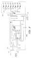
- FIG. 3is a schematic diagram according to an embodiment of the invention illustrating an exemplary destroy circuit 214 and an exemplary destroy isolation circuit 222 usable by the NVM storage system 120 shown in FIG. 2 .
- the destroy circuit 214comprises destroy control logic 218 and a voltage converter circuit 220 .
- the voltage converter circuit 220comprises a DC-to-DC converter 310 and a power MOSFET 312 configured in a “fly-back” or “charge pump” configuration.
- the DC-to-DC converter 310comprises a MAX668 pulse-width modulating (PWM) step-up controller available from Maxim Integrated Products, Inc. of Sunnyvale Calif.
- PWMpulse-width modulating
- the destroy control logic 218is configured to activate the DC-to-DC converter 310 when it receives the VCC signal 125 and the Destroy control signal 221 .
- the DC-to-DC converter 310is configured to drive the power MOSFET 312 to generate the VOUT signal 226 . Exemplary voltage level and current levels for the VOUT signal 226 are provided above.
- the VOUT signal 226is provided through a diode D 1 to the destroy isolation circuit 222 .
- the destroy isolation circuit 222comprises an optoisolator 314 and a diode array 316 comprising a plurality of diodes (eight shown as diodes D 3 -D 10 ).
- the optoisolator 314is controlled by the destroy control signal 221 .
- the optoisolator 314sinks the VOUT signal's current.
- the destroy control signal 221activates the DC-to-DC converter 310 , it also activates the optoisolator 314 so as to provide the VOUT signal 226 to the diode array 316 .
- the diode array 316is configured to couple the VOUT signal 226 to memory device input pins (i.e., control or command pins) and/or output pins.
- the input and/or output pinsare represented by HD 0 -HD 7 .
- the diode array 316is connected in parallel to two or more memory devices in the NVM array. Thus, the destroy circuit 214 physically damages the memory devices at the same time, saving time and power.
- VOUT signal 226to an input pin of a memory device damages a portion of the semiconductor material. However, it may also create short circuits that prevent additional damage to other portions of semiconductor material when the VOUT signal 226 is applied to other input pins.
- the diode array 316is configured to apply the VOUT signal 226 to a plurality of input pins of a particular memory device at the same time.
- the VOUT signal 226is applied to one or more output pins after being applied to the input pins. For example, in one embodiment a substantial amount of damage is caused by applying the VOUT signal 226 to one input pin and four output pins.
- FIGS. 4A and 4Billustrate exemplary command formats for a first purge command 400 and a second purge command 410 according to an embodiment of the invention.
- the first purge command 400 and the second purge command 410are vendor specific commands in the ATA command set and, as such, include register fields to specify features, sector count, sector number, cylinder low, cylinder high, drive head, and command information.
- each register fieldincludes eight bits (i.e., D 0 -D 7 ).
- An “X”indicates that the corresponding portion of the register field can have any value.
- the first purge command 400 and the second purge command 410may be sent, for example, as control signals 122 from the host system 110 to the NVM controller 114 shown in FIGS. 1 or 2 .
- the NVM controller 114will not execute the purge commands, however, unless the first purge command 400 and the second purge command 410 are received in sequence. Thus, the likelihood of inadvertently performing a purge function is reduced.
- the first purge command 400indicates that the host system 110 has initiated a purge operation.
- the purge operationmay be a non-destructive purge operation or a destructive purge operation.
- a non-destructive purge operationerases the user data blocks.
- the non-destructive purge operationalso writes a pattern to the user data blocks.
- erasing data and writing a pattern to user data blocksare separate operations and the storage system 110 sends a unique set of purge commands 400 , 410 for each.
- a destructive purge operationerases the user data blocks along with other data including firmware, bad block table, parity data, and control structures stored in the NVM array 116 .
- the destructive purge operationrenders the storage system inoperable.
- the destructive purge operationalso causes physical damage to the memory devices using, for example, the destroy circuit 214 shown in FIG. 2 .
- rendering the storage system inoperable and physically damaging the memory devicesare separate operations and the host system 110 sends a unique set of purge commands 400 , 410 for each.
- one set of purge commands 400 , 410instructs the NVM controller 114 to purge the NVM array 116 in two phases.
- the NVM controller 114erases and/or writes a pattern to the memory devices.
- the NVM controller 114physically damages the memory devices, as discussed herein.
- the NVM controller 114cannot destroy all of the memory devices due to, for example, failure of the internal battery 128 , the data therein will still have been erased and/or written over.
- the host system 110can pass more control to the NVM controller 114 when it sends the first purge command 400 and the second purge command 410 .
- the host system 110can send one set of purge commands 400 , 410 to the NVM controller 114 .
- the NVM controller 114can then perform each of these functions without further instructions from the host system 110 .
- the host system 110After the host system 110 initiates the purge operation by sending the first purge command 400 , the host system 110 then specifies the specific purge operation by sending the second purge command 410 to the NVM controller 114 .
- the host system 110sets the feature register 412 in the second purge command 410 to “0” to initiate a non-destructive purge operation and “1” to initiate a destructive purge operation.
- the feature register 412 in the second purge command 410can specify other operations or combinations of operations.
- the sector count register 414 in the second purge command 410defines the number of memory devices to be erased at a time and the sector number register 416 in the second purge command 410 defines a data pattern to write to the memory devices. If, for example, the sector count register 414 specifies erasing four memory devices at a time, the NVM controller 114 erases a first set of four memory devices in parallel. Once the first set of four memory devices is erased, the NVM controller 114 erases a second set of four memory devices in parallel. The NVM controller 114 repeats this process until all of the memory devices in the NVM array 116 are erased.
- FIG. 5illustrates a first graph 510 and a second graph 520 showing the relationship between the amount of time spent erasing a memory array (i.e., “purge time”) and the current consumed while erasing the memory array (i.e., “purge current”).
- the exemplary graphs 510 , 520corresponds to erasing a memory array comprising sixteen 1 Gb flash memory devices.
- the first graph 510corresponds to typical measured values for the purge time versus the purge current.
- the second graph 520corresponds to expected maximum values for the purge time versus the purge current. Data points are shown for erasing one memory device at a time, two memory devices at a time, four memory devices at a time, eight memory devices at a time, and all sixteen memory devices at a time.
- the least amount of currentis consumed when the sixteen memory devices are erased one at a time. However, erasing the memory devices sequentially also takes the most time. As more memory devices are erased in parallel, the purge time decreases and the purge current increases. The quickest purge times occur when all sixteen memory devices are erased in parallel. However, this also uses the most purge current. Thus, there is a trade-off between purge time and purge current.
- the sector count register 414 in the second purge command 410allows a programmer of the host system's computer program, as discussed above, to specify the number of memory devices to erase at a time.
- the programmercan selectively specify the number of memory devices to erase in parallel based on factors such as the power available in a particular application, the overall number of memory devices to erase, the size of the memory devices (i.e., the number of bytes), personal preference, the urgency of a particular situation, combinations of the forgoing, or the like.
- the programmercan selectively specify the number of memory devices to physically damage at a time.
- the NVM controller 114can respond to the second purge command 410 by selecting the number of memory devices to erase and/or destroy at a time.
- the NVM controller 114can selectively specify the number of memory devices to erase and/or physically damage in parallel based on factors such as a state of the internal battery 128 , disconnection from the host system 110 , and/or other criteria. For example, the NVM controller 114 may monitor the power remaining in the internal battery 128 and alter the number of memory devices when the power drops below a predetermined level.
Landscapes
- Engineering & Computer Science (AREA)
- Computer Security & Cryptography (AREA)
- Theoretical Computer Science (AREA)
- Computer Hardware Design (AREA)
- Physics & Mathematics (AREA)
- General Engineering & Computer Science (AREA)
- General Physics & Mathematics (AREA)
- Software Systems (AREA)
- Techniques For Improving Reliability Of Storages (AREA)
- Storage Device Security (AREA)
Abstract
Description
Claims (13)
Priority Applications (1)
| Application Number | Priority Date | Filing Date | Title |
|---|---|---|---|
| US12/399,654US7898855B2 (en) | 2004-11-30 | 2009-03-06 | Systems and methods for reducing unauthorized data recovery from solid-state storage devices |
Applications Claiming Priority (2)
| Application Number | Priority Date | Filing Date | Title |
|---|---|---|---|
| US11/000,134US7502256B2 (en) | 2004-11-30 | 2004-11-30 | Systems and methods for reducing unauthorized data recovery from solid-state storage devices |
| US12/399,654US7898855B2 (en) | 2004-11-30 | 2009-03-06 | Systems and methods for reducing unauthorized data recovery from solid-state storage devices |
Related Parent Applications (1)
| Application Number | Title | Priority Date | Filing Date |
|---|---|---|---|
| US11/000,134ContinuationUS7502256B2 (en) | 2004-11-30 | 2004-11-30 | Systems and methods for reducing unauthorized data recovery from solid-state storage devices |
Publications (2)
| Publication Number | Publication Date |
|---|---|
| US20090196100A1 US20090196100A1 (en) | 2009-08-06 |
| US7898855B2true US7898855B2 (en) | 2011-03-01 |
Family
ID=36568641
Family Applications (4)
| Application Number | Title | Priority Date | Filing Date |
|---|---|---|---|
| US11/000,134Expired - Fee RelatedUS7502256B2 (en) | 2004-11-30 | 2004-11-30 | Systems and methods for reducing unauthorized data recovery from solid-state storage devices |
| US11/458,336Expired - Fee RelatedUS7430136B2 (en) | 2004-11-30 | 2006-07-18 | Purge operations for solid-state storage devices |
| US12/240,579Expired - Fee RelatedUS7936603B2 (en) | 2004-11-30 | 2008-09-29 | Purge operations for solid-state storage devices |
| US12/399,654Expired - LifetimeUS7898855B2 (en) | 2004-11-30 | 2009-03-06 | Systems and methods for reducing unauthorized data recovery from solid-state storage devices |
Family Applications Before (3)
| Application Number | Title | Priority Date | Filing Date |
|---|---|---|---|
| US11/000,134Expired - Fee RelatedUS7502256B2 (en) | 2004-11-30 | 2004-11-30 | Systems and methods for reducing unauthorized data recovery from solid-state storage devices |
| US11/458,336Expired - Fee RelatedUS7430136B2 (en) | 2004-11-30 | 2006-07-18 | Purge operations for solid-state storage devices |
| US12/240,579Expired - Fee RelatedUS7936603B2 (en) | 2004-11-30 | 2008-09-29 | Purge operations for solid-state storage devices |
Country Status (1)
| Country | Link |
|---|---|
| US (4) | US7502256B2 (en) |
Cited By (127)
| Publication number | Priority date | Publication date | Assignee | Title |
|---|---|---|---|---|
| US20130250663A1 (en)* | 2012-03-26 | 2013-09-26 | Honeywell International Inc. | Anti-tampering devices and techniques for magnetoresistive random access memory |
| US8730715B2 (en) | 2012-03-26 | 2014-05-20 | Honeywell International Inc. | Tamper-resistant MRAM utilizing chemical alteration |
| US8816717B2 (en) | 2012-10-17 | 2014-08-26 | International Business Machines Corporation | Reactive material for integrated circuit tamper detection and response |
| US8861728B2 (en) | 2012-10-17 | 2014-10-14 | International Business Machines Corporation | Integrated circuit tamper detection and response |
| US8860176B2 (en) | 2012-10-17 | 2014-10-14 | International Business Machines Corporation | Multi-doped silicon antifuse device for integrated circuit |
| US8898373B1 (en) | 2011-06-29 | 2014-11-25 | Western Digital Technologies, Inc. | System and method for improving wear-leveling performance in solid-state memory |
| US8917471B1 (en) | 2013-10-29 | 2014-12-23 | Western Digital Technologies, Inc. | Power management for data storage device |
| US8954694B2 (en) | 2012-11-15 | 2015-02-10 | Western Digital Technologies, Inc. | Methods, data storage devices and systems for fragmented firmware table rebuild in a solid state drive |
| US8954655B2 (en) | 2013-01-14 | 2015-02-10 | Western Digital Technologies, Inc. | Systems and methods of configuring a mode of operation in a solid-state memory |
| US8954653B1 (en) | 2012-06-26 | 2015-02-10 | Western Digital Technologies, Inc. | Mechanisms for efficient management of system data in data storage systems |
| US8959416B1 (en) | 2011-12-16 | 2015-02-17 | Western Digital Technologies, Inc. | Memory defect management using signature identification |
| US8959284B1 (en) | 2010-06-28 | 2015-02-17 | Western Digital Technologies, Inc. | Disk drive steering write data to write cache based on workload |
| US8966205B1 (en) | 2012-05-10 | 2015-02-24 | Western Digital Technologies, Inc. | System data management using garbage collection and hybrid self mapping |
| US8966339B1 (en) | 2012-12-18 | 2015-02-24 | Western Digital Technologies, Inc. | Decoder supporting multiple code rates and code lengths for data storage systems |
| US8966343B2 (en) | 2012-08-21 | 2015-02-24 | Western Digital Technologies, Inc. | Solid-state drive retention monitor using reference blocks |
| US8972826B2 (en) | 2012-10-24 | 2015-03-03 | Western Digital Technologies, Inc. | Adaptive error correction codes for data storage systems |
| US8972655B2 (en) | 2013-01-21 | 2015-03-03 | Western Digital Technolgies, Inc. | Initialization of a storage device |
| US8977804B1 (en) | 2011-11-21 | 2015-03-10 | Western Digital Technologies, Inc. | Varying data redundancy in storage systems |
| US8984247B1 (en) | 2012-05-10 | 2015-03-17 | Western Digital Technologies, Inc. | Storing and reconstructing mapping table data in a data storage system |
| US8990668B2 (en) | 2013-03-14 | 2015-03-24 | Western Digital Technologies, Inc. | Decoding data stored in solid-state memory |
| US9007841B1 (en) | 2013-10-24 | 2015-04-14 | Western Digital Technologies, Inc. | Programming scheme for improved voltage distribution in solid-state memory |
| US9007854B1 (en) | 2013-12-09 | 2015-04-14 | Western Digital Technologies, Inc. | Method and system for optimized soft decoding in a data storage device |
| US9013920B2 (en) | 2013-04-03 | 2015-04-21 | Western Digital Technologies, Inc. | Systems and methods of write precompensation to extend life of a solid-state memory |
| US9021192B1 (en) | 2010-09-21 | 2015-04-28 | Western Digital Technologies, Inc. | System and method for enhancing processing of memory access requests |
| US9021339B2 (en) | 2012-11-29 | 2015-04-28 | Western Digital Technologies, Inc. | Data reliability schemes for data storage systems |
| US9021168B1 (en) | 2011-09-06 | 2015-04-28 | Western Digital Technologies, Inc. | Systems and methods for an enhanced controller architecture in data storage systems |
| US9026716B2 (en) | 2010-05-12 | 2015-05-05 | Western Digital Technologies, Inc. | System and method for managing garbage collection in solid-state memory |
| US9032271B2 (en) | 2012-12-07 | 2015-05-12 | Western Digital Technologies, Inc. | System and method for lower page data recovery in a solid state drive |
| US9036283B1 (en) | 2014-01-22 | 2015-05-19 | Western Digital Technologies, Inc. | Data storage device with selective write to a first storage media or a second storage media |
| US9042197B2 (en) | 2013-07-23 | 2015-05-26 | Western Digital Technologies, Inc. | Power fail protection and recovery using low power states in a data storage device/system |
| US9053008B1 (en) | 2012-03-26 | 2015-06-09 | Western Digital Technologies, Inc. | Systems and methods for providing inline parameter service in data storage devices |
| US9059736B2 (en) | 2012-12-03 | 2015-06-16 | Western Digital Technologies, Inc. | Methods, solid state drive controllers and data storage devices having a runtime variable raid protection scheme |
| US9058280B1 (en) | 2010-08-13 | 2015-06-16 | Western Digital Technologies, Inc. | Hybrid drive migrating data from disk to non-volatile semiconductor memory based on accumulated access time |
| US9059742B1 (en) | 2013-03-15 | 2015-06-16 | Western Digital Technologies, Inc. | System and method for dynamic scaling of LDPC decoder in a solid state drive |
| US9058261B1 (en) | 2011-09-06 | 2015-06-16 | Western Digital Technologies, Inc. | Systems and methods for detailed error reporting in data storage systems |
| US9069475B1 (en) | 2010-10-26 | 2015-06-30 | Western Digital Technologies, Inc. | Hybrid drive selectively spinning up disk when powered on |
| US9070379B2 (en) | 2013-08-28 | 2015-06-30 | Western Digital Technologies, Inc. | Data migration for data storage device |
| US9081700B2 (en) | 2013-05-16 | 2015-07-14 | Western Digital Technologies, Inc. | High performance read-modify-write system providing line-rate merging of dataframe segments in hardware |
| US9110835B1 (en) | 2011-03-09 | 2015-08-18 | Western Digital Technologies, Inc. | System and method for improving a data redundancy scheme in a solid state subsystem with additional metadata |
| US9122625B1 (en) | 2012-12-18 | 2015-09-01 | Western Digital Technologies, Inc. | Error correcting code encoder supporting multiple code rates and throughput speeds for data storage systems |
| US9123686B2 (en) | 2013-04-12 | 2015-09-01 | Western Digital Technologies, Inc. | Thermal management for solid-state drive |
| US9141176B1 (en) | 2013-07-29 | 2015-09-22 | Western Digital Technologies, Inc. | Power management for data storage device |
| US9164886B1 (en) | 2010-09-21 | 2015-10-20 | Western Digital Technologies, Inc. | System and method for multistage processing in a memory storage subsystem |
| US9170938B1 (en) | 2013-05-17 | 2015-10-27 | Western Digital Technologies, Inc. | Method and system for atomically writing scattered information in a solid state storage device |
| US9170932B1 (en) | 2012-05-22 | 2015-10-27 | Western Digital Technologies, Inc. | System data storage mechanism providing coherency and segmented data loading |
| US9176859B2 (en) | 2009-01-07 | 2015-11-03 | Siliconsystems, Inc. | Systems and methods for improving the performance of non-volatile memory operations |
| US9177638B2 (en) | 2012-11-13 | 2015-11-03 | Western Digital Technologies, Inc. | Methods and devices for avoiding lower page corruption in data storage devices |
| US9182916B1 (en) | 2010-09-17 | 2015-11-10 | Western Digital Technologies, Inc. | Non-volatile storage subsystem with energy-based performance throttling |
| US9195530B1 (en) | 2011-09-06 | 2015-11-24 | Western Digital Technologies, Inc. | Systems and methods for improved data management in data storage systems |
| US9195293B1 (en) | 2013-05-03 | 2015-11-24 | Western Digital Technologies, Inc. | User controlled data storage device power and performance settings |
| US9208101B2 (en) | 2013-06-26 | 2015-12-08 | Western Digital Technologies, Inc. | Virtual NAND capacity extension in a hybrid drive |
| US9208020B2 (en) | 2012-06-26 | 2015-12-08 | Western Digital Technologies, Inc. | Efficient error handling mechanisms in data storage systems |
| US9214963B1 (en) | 2012-12-21 | 2015-12-15 | Western Digital Technologies, Inc. | Method and system for monitoring data channel to enable use of dynamically adjustable LDPC coding parameters in a data storage system |
| US9218279B2 (en) | 2013-03-15 | 2015-12-22 | Western Digital Technologies, Inc. | Atomic write command support in a solid state drive |
| US9250994B1 (en) | 2014-02-05 | 2016-02-02 | Western Digital Technologies, Inc. | Non-binary low-density parity check (LDPC) decoding using trellis maximization |
| US9263136B1 (en) | 2013-09-04 | 2016-02-16 | Western Digital Technologies, Inc. | Data retention flags in solid-state drives |
| US9268701B1 (en) | 2011-11-21 | 2016-02-23 | Western Digital Technologies, Inc. | Caching of data in data storage systems by managing the size of read and write cache based on a measurement of cache reliability |
| US9270296B1 (en) | 2013-11-13 | 2016-02-23 | Western Digital Technologies, Inc. | Method and system for soft decoding through single read |
| US9268487B2 (en) | 2014-03-24 | 2016-02-23 | Western Digital Technologies, Inc. | Method and apparatus for restricting writes to solid state memory when an end-of life condition is reached |
| US9274978B2 (en) | 2013-06-10 | 2016-03-01 | Western Digital Technologies, Inc. | Migration of encrypted data for data storage systems |
| US9275741B1 (en) | 2014-09-10 | 2016-03-01 | Western Digital Technologies, Inc. | Temperature compensation management in solid-state memory |
| US9274966B1 (en) | 2013-02-20 | 2016-03-01 | Western Digital Technologies, Inc. | Dynamically throttling host commands to disk drives |
| US9280200B1 (en) | 2013-05-20 | 2016-03-08 | Western Digital Technologies, Inc. | Automatic peak current throttle of tiered storage elements |
| US9280472B1 (en) | 2013-03-13 | 2016-03-08 | Western Digital Technologies, Inc. | Caching data in a high performance zone of a data storage system |
| US9286176B1 (en) | 2013-11-08 | 2016-03-15 | Western Digital Technologies, Inc. | Selective skipping of blocks in an SSD |
| US9304709B2 (en) | 2013-09-06 | 2016-04-05 | Western Digital Technologies, Inc. | High performance system providing selective merging of dataframe segments in hardware |
| US9304560B2 (en) | 2013-06-19 | 2016-04-05 | Western Digital Technologies, Inc. | Backup power for reducing host current transients |
| US9323467B2 (en) | 2013-10-29 | 2016-04-26 | Western Digital Technologies, Inc. | Data storage device startup |
| US9330143B2 (en) | 2013-10-24 | 2016-05-03 | Western Digital Technologies, Inc. | Data storage device supporting accelerated database operations |
| US9337864B1 (en) | 2014-01-29 | 2016-05-10 | Western Digital Technologies, Inc. | Non-binary LDPC decoder using binary subgroup processing |
| US9338927B2 (en) | 2013-05-02 | 2016-05-10 | Western Digital Technologies, Inc. | Thermal interface material pad and method of forming the same |
| US9335950B2 (en) | 2013-03-15 | 2016-05-10 | Western Digital Technologies, Inc. | Multiple stream compression and formatting of data for data storage systems |
| US9348520B2 (en) | 2014-03-24 | 2016-05-24 | Western Digital Technologies, Inc. | Lifetime extension of non-volatile semiconductor memory for data storage device |
| US9348741B1 (en) | 2011-12-19 | 2016-05-24 | Western Digital Technologies, Inc. | Systems and methods for handling write data access requests in data storage devices |
| US9354955B1 (en) | 2014-03-19 | 2016-05-31 | Western Digital Technologies, Inc. | Partial garbage collection for fast error handling and optimized garbage collection for the invisible band |
| US9361044B2 (en) | 2011-03-28 | 2016-06-07 | Western Digital Technologies, Inc. | Power-safe data management system |
| US9384088B1 (en) | 2014-02-24 | 2016-07-05 | Western Digital Technologies, Inc. | Double writing map table entries in a data storage system to guard against silent corruption |
| US9405675B1 (en) | 2010-05-11 | 2016-08-02 | Western Digital Technologies, Inc. | System and method for managing execution of internal commands and host commands in a solid-state memory |
| US9405617B1 (en) | 2011-02-11 | 2016-08-02 | Western Digital Technologies, Inc. | System and method for data error recovery in a solid state subsystem |
| US9405356B1 (en) | 2014-10-21 | 2016-08-02 | Western Digital Technologies, Inc. | Temperature compensation in data storage device |
| US9418699B1 (en) | 2014-10-09 | 2016-08-16 | Western Digital Technologies, Inc. | Management of sequentially written data |
| US9436630B2 (en) | 2013-06-11 | 2016-09-06 | Western Digital Technologies, Inc. | Using dual phys to support multiple PCIe link widths |
| US9436401B1 (en) | 2015-03-23 | 2016-09-06 | International Business Machines Corporation | Computer memory data security |
| US9442668B1 (en) | 2013-08-29 | 2016-09-13 | Western Digital Technologies, Inc. | Adaptive power management control with performance feedback |
| US9448738B2 (en) | 2013-03-15 | 2016-09-20 | Western Digital Technologies, Inc. | Compression and formatting of data for data storage systems |
| US9448742B2 (en) | 2014-03-27 | 2016-09-20 | Western Digital Technologies, Inc. | Communication between a host and a secondary storage device |
| US9454474B2 (en) | 2013-03-05 | 2016-09-27 | Western Digital Technologies, Inc. | Methods, devices and systems for two stage power-on map rebuild with free space accounting in a solid state drive |
| US9472222B2 (en) | 2014-05-16 | 2016-10-18 | Western Digital Technologies, Inc. | Vibration mitigation for a data storage device |
| US9489296B1 (en) | 2012-10-17 | 2016-11-08 | Western Digital Technologies, Inc. | Methods, devices and systems for hardware-based garbage collection in solid state drives |
| US9507523B1 (en) | 2012-10-12 | 2016-11-29 | Western Digital Technologies, Inc. | Methods, devices and systems for variable size logical page management in a solid state drive |
| US9529710B1 (en) | 2013-12-06 | 2016-12-27 | Western Digital Technologies, Inc. | Interleaved channels in a solid-state drive |
| US9542287B1 (en) | 2011-09-06 | 2017-01-10 | Western Digital Technologies, Inc. | Systems and methods for error injection in data storage systems |
| US9564212B2 (en) | 2014-05-06 | 2017-02-07 | Western Digital Technologies, Inc. | Solid-state memory corruption mitigation |
| US9583153B1 (en) | 2013-06-28 | 2017-02-28 | Western Digital Technologies, Inc. | Memory card placement within a solid state drive |
| US9620226B1 (en) | 2015-10-30 | 2017-04-11 | Western Digital Technologies, Inc. | Data retention charge loss and read disturb compensation in solid-state data storage systems |
| US9619317B1 (en) | 2012-12-18 | 2017-04-11 | Western Digital Technologies, Inc. | Decoder having early decoding termination detection |
| US9641378B1 (en) | 2013-03-12 | 2017-05-02 | Western Digital Technologies, Inc. | Adjustment of compression ratios for data storage |
| US9652379B1 (en) | 2010-09-15 | 2017-05-16 | Western Digital Technologies, Inc. | System and method for reducing contentions in solid-state memory access |
| US9665501B1 (en) | 2013-06-18 | 2017-05-30 | Western Digital Technologies, Inc. | Self-encrypting data storage device supporting object-level encryption |
| US9668337B2 (en) | 2015-09-08 | 2017-05-30 | Western Digital Technologies, Inc. | Temperature management in data storage devices |
| US9690696B1 (en) | 2014-05-14 | 2017-06-27 | Western Digital Technologies, Inc. | Lifetime extension of memory for data storage system |
| US9727261B2 (en) | 2015-09-24 | 2017-08-08 | Western Digital Technologies, Inc. | Weighted programming patterns in solid-state data storage systems |
| US9740248B2 (en) | 2013-06-07 | 2017-08-22 | Western Digital Technologies, Inc. | Component placement within a solid state drive |
| US9753847B2 (en) | 2009-10-27 | 2017-09-05 | Western Digital Technologies, Inc. | Non-volatile semiconductor memory segregating sequential, random, and system data to reduce garbage collection for page based mapping |
| US9785563B1 (en) | 2015-08-13 | 2017-10-10 | Western Digital Technologies, Inc. | Read command processing for data storage system based on previous writes |
| US9823859B2 (en) | 2014-11-06 | 2017-11-21 | Western Digital Technologies, Inc. | Mechanical shock mitigation for data storage |
| US9830257B1 (en) | 2013-06-12 | 2017-11-28 | Western Digital Technologies, Inc. | Fast saving of data during power interruption in data storage systems |
| US9836232B1 (en) | 2015-09-30 | 2017-12-05 | Western Digital Technologies, Inc. | Data storage device and method for using secondary non-volatile memory for temporary metadata storage |
| US9857995B1 (en) | 2015-03-09 | 2018-01-02 | Western Digital Technologies, Inc. | Data storage device and method providing non-volatile memory buffer for real-time primary non-volatile memory protection |
| US9977612B1 (en) | 2012-05-11 | 2018-05-22 | Western Digital Technologies, Inc. | System data management using garbage collection and logs |
| US10013174B2 (en) | 2015-09-30 | 2018-07-03 | Western Digital Technologies, Inc. | Mapping system selection for data storage device |
| US10079048B2 (en) | 2009-03-24 | 2018-09-18 | Western Digital Technologies, Inc. | Adjusting access of non-volatile semiconductor memory based on access time |
| US10126981B1 (en) | 2015-12-14 | 2018-11-13 | Western Digital Technologies, Inc. | Tiered storage using storage class memory |
| US10140067B1 (en) | 2013-12-19 | 2018-11-27 | Western Digital Technologies, Inc. | Data management for data storage device with multiple types of non-volatile memory media |
| US10387303B2 (en) | 2016-08-16 | 2019-08-20 | Western Digital Technologies, Inc. | Non-volatile storage system with compute engine to accelerate big data applications |
| US10417123B1 (en) | 2013-05-16 | 2019-09-17 | Western Digital Technologies, Inc. | Systems and methods for improving garbage collection and wear leveling performance in data storage systems |
| US10444998B1 (en) | 2013-10-24 | 2019-10-15 | Western Digital Technologies, Inc. | Data storage device providing data maintenance services |
| US10459644B2 (en) | 2016-10-28 | 2019-10-29 | Western Digital Techologies, Inc. | Non-volatile storage system with integrated compute engine and optimized use of local fast memory |
| US10545819B1 (en) | 2013-03-12 | 2020-01-28 | Western Digital Technologies, Inc. | Soft-decision input generation for data storage systems |
| US10565123B2 (en) | 2017-04-10 | 2020-02-18 | Western Digital Technologies, Inc. | Hybrid logical to physical address translation for non-volatile storage devices with integrated compute module |
| US10740231B2 (en) | 2018-11-20 | 2020-08-11 | Western Digital Technologies, Inc. | Data access in data storage device including storage class memory |
| US10769062B2 (en) | 2018-10-01 | 2020-09-08 | Western Digital Technologies, Inc. | Fine granularity translation layer for data storage devices |
| US10956071B2 (en) | 2018-10-01 | 2021-03-23 | Western Digital Technologies, Inc. | Container key value store for data storage devices |
| US11016905B1 (en) | 2019-11-13 | 2021-05-25 | Western Digital Technologies, Inc. | Storage class memory access |
| US11249921B2 (en) | 2020-05-06 | 2022-02-15 | Western Digital Technologies, Inc. | Page modification encoding and caching |
| US11487657B1 (en)* | 2013-01-28 | 2022-11-01 | Radian Memory Systems, Inc. | Storage system with multiplane segments and cooperative flash management |
| US12147335B1 (en) | 2013-01-28 | 2024-11-19 | Radian Memory Systems, LLC | Cooperative storage device for managing logical subdivisions |
Families Citing this family (61)
| Publication number | Priority date | Publication date | Assignee | Title |
|---|---|---|---|---|
| JP4125277B2 (en)* | 2004-09-22 | 2008-07-30 | キヤノン株式会社 | Image forming apparatus and data erasing method |
| US7502256B2 (en) | 2004-11-30 | 2009-03-10 | Siliconsystems, Inc. | Systems and methods for reducing unauthorized data recovery from solid-state storage devices |
| US20060152173A1 (en)* | 2004-12-27 | 2006-07-13 | M-Systems Flash Disk Pioneers Ltd. | Method and apparatus for intentionally damaging a solid-state disk |
| KR100704037B1 (en)* | 2005-04-15 | 2007-04-04 | 삼성전자주식회사 | Data storage device having heterogeneous nonvolatile memory and its driving method |
| US8321953B2 (en)* | 2005-07-14 | 2012-11-27 | Imation Corp. | Secure storage device with offline code entry |
| US8015606B1 (en) | 2005-07-14 | 2011-09-06 | Ironkey, Inc. | Storage device with website trust indication |
| US8335920B2 (en)* | 2005-07-14 | 2012-12-18 | Imation Corp. | Recovery of data access for a locked secure storage device |
| US8438647B2 (en)* | 2005-07-14 | 2013-05-07 | Imation Corp. | Recovery of encrypted data from a secure storage device |
| US20070067620A1 (en)* | 2005-09-06 | 2007-03-22 | Ironkey, Inc. | Systems and methods for third-party authentication |
| US7450436B2 (en)* | 2005-10-17 | 2008-11-11 | Stec, Inc. | Device recoverable purge for flash storage device |
| US20070101048A1 (en)* | 2005-10-17 | 2007-05-03 | Simpletech, Inc. | Verified purge for flash storage device |
| JP4955990B2 (en)* | 2005-12-14 | 2012-06-20 | 株式会社東芝 | Nonvolatile semiconductor memory device |
| US8266378B1 (en) | 2005-12-22 | 2012-09-11 | Imation Corp. | Storage device with accessible partitions |
| US8639873B1 (en) | 2005-12-22 | 2014-01-28 | Imation Corp. | Detachable storage device with RAM cache |
| US7793059B2 (en)* | 2006-01-18 | 2010-09-07 | Apple Inc. | Interleaving policies for flash memory |
| US20070300031A1 (en)* | 2006-06-22 | 2007-12-27 | Ironkey, Inc. | Memory data shredder |
| KR100782113B1 (en)* | 2006-11-13 | 2007-12-05 | 삼성전자주식회사 | Memory card system and its host identification information transmission method |
| US20080201520A1 (en)* | 2007-02-03 | 2008-08-21 | Stec, Inc. | Flash firmware management |
| US7532027B2 (en)* | 2007-09-28 | 2009-05-12 | Adtron, Inc. | Deliberate destruction of integrated circuits |
| US20090172251A1 (en)* | 2007-12-26 | 2009-07-02 | Unity Semiconductor Corporation | Memory Sanitization |
| WO2009137371A2 (en)* | 2008-05-02 | 2009-11-12 | Ironkey, Inc. | Enterprise device recovery |
| GB2460275B (en)* | 2008-05-23 | 2012-12-19 | Exacttrak Ltd | A Communications and Security Device |
| US8407401B2 (en)* | 2008-11-26 | 2013-03-26 | Core Wireless Licensing S.A.R.L. | Methods, apparatuses, and computer program products for enhancing memory erase functionality |
| US20100131726A1 (en)* | 2008-11-26 | 2010-05-27 | Nokia Corporation | Methods, apparatuses, and computer program products for enhancing memory erase functionality |
| US20100228906A1 (en)* | 2009-03-06 | 2010-09-09 | Arunprasad Ramiya Mothilal | Managing Data in a Non-Volatile Memory System |
| FR2943153B1 (en)* | 2009-03-13 | 2014-09-12 | Airbus France | AIRCRAFT COMPRISING MEANS OF DESTRUCTION OF DATA |
| US7982488B2 (en)* | 2009-05-29 | 2011-07-19 | Infineon Technologies Ag | Phase-change memory security device |
| US8745365B2 (en)* | 2009-08-06 | 2014-06-03 | Imation Corp. | Method and system for secure booting a computer by booting a first operating system from a secure peripheral device and launching a second operating system stored a secure area in the secure peripheral device on the first operating system |
| US8683088B2 (en) | 2009-08-06 | 2014-03-25 | Imation Corp. | Peripheral device data integrity |
| US8560764B2 (en)* | 2009-12-21 | 2013-10-15 | Intel Corporation | Repurposing NAND ready/busy pin as completion interrupt |
| US9330753B2 (en) | 2010-11-29 | 2016-05-03 | Seagate Technology Llc | Memory sanitation using bit-inverted data |
| CN102568559A (en)* | 2010-12-17 | 2012-07-11 | 西安奇维测控科技有限公司 | A method for double data destruction of electronic disk |
| TWI479493B (en)* | 2011-04-25 | 2015-04-01 | Silicon Motion Inc | Flash memory device and power failure handling method thereof |
| US9015401B2 (en) | 2011-04-28 | 2015-04-21 | Seagate Technology Llc | Selective purge of confidential data from a non-volatile memory |
| US8832402B2 (en)* | 2011-04-29 | 2014-09-09 | Seagate Technology Llc | Self-initiated secure erasure responsive to an unauthorized power down event |
| US8705291B2 (en) | 2011-05-27 | 2014-04-22 | Seagate Technology Llc | Sanitizing a non-volatile memory through charge accumulation |
| US8909942B1 (en)* | 2012-03-30 | 2014-12-09 | Western Digital Technologies, Inc. | MRAM-based security for data storage systems |
| CN202615309U (en)* | 2012-04-02 | 2012-12-19 | 鸿富锦精密工业(深圳)有限公司 | Power supply device |
| US8938626B2 (en) | 2012-07-17 | 2015-01-20 | Dell Products, L.P. | Single command functionality for providing data security and preventing data access within a decommissioned information handling system |
| WO2015026826A1 (en)* | 2013-08-21 | 2015-02-26 | Everspin Technologies, Inc. | Non-destructive write/read leveling |
| US9244627B2 (en)* | 2013-10-15 | 2016-01-26 | Synetic Technologies, Inc. | Secure data erasure system for erasing a plurality of data storage devices |
| WO2015164576A1 (en)* | 2014-04-23 | 2015-10-29 | Ensconce Data Technology, Llc. | Method for completing a secure erase operation |
| US9755649B1 (en)* | 2015-02-09 | 2017-09-05 | Xilinx, Inc. | Protection against tamper using in-rush current |
| CN105989310B (en)* | 2015-03-03 | 2019-11-26 | 联想(北京)有限公司 | A kind of data destruction method and system |
| CN108780491A (en)* | 2015-11-03 | 2018-11-09 | Ictk控股有限公司 | Safety device and its operating method |
| US9941004B2 (en) | 2015-12-30 | 2018-04-10 | International Business Machines Corporation | Integrated arming switch and arming switch activation layer for secure memory |
| US10528769B2 (en)* | 2017-07-23 | 2020-01-07 | Albert C. Abnett | Method and apparatus for destroying nonvolatile computer memory |
| US10579288B2 (en) | 2017-08-31 | 2020-03-03 | Micron Technology, Inc. | Prioritized security |
| KR102411290B1 (en) | 2017-10-24 | 2022-06-22 | 삼성전자주식회사 | Storage system including host device and storage device configured to perform selective purge operation |
| CN113760185B (en) | 2017-11-07 | 2024-09-24 | 华为技术有限公司 | Memory block recycling method and device |
| US10446248B1 (en) | 2018-04-23 | 2019-10-15 | Micron Technology, Inc. | Non-volatile memory devices and systems with read-only memory features and methods for operating the same |
| US11049565B2 (en)* | 2018-04-23 | 2021-06-29 | Micron Technology, Inc. | Non-volatile memory devices and systems with volatile memory features and methods for operating the same |
| US11630496B1 (en)* | 2018-06-28 | 2023-04-18 | Amazon Technologies, Inc. | Distributed computing device power |
| US11003551B2 (en) | 2018-09-27 | 2021-05-11 | Sandisk Technologies Llc | Non-volatile storage system with program failure recovery |
| US11455402B2 (en) | 2019-01-30 | 2022-09-27 | Seagate Technology Llc | Non-volatile memory with precise write-once protection |
| US11681965B2 (en)* | 2019-10-25 | 2023-06-20 | Georgetown University | Specialized computing environment for co-analysis of proprietary data |
| US11675524B2 (en)* | 2020-08-17 | 2023-06-13 | Crystal Group, Inc. | Isolated hardware data sanitize system and method |
| JP7413300B2 (en)* | 2021-03-15 | 2024-01-15 | 株式会社東芝 | Storage device |
| KR20230166803A (en) | 2022-05-30 | 2023-12-07 | 삼성전자주식회사 | Storage device providing high purge performance and memory block management method thereof |
| US12333167B2 (en)* | 2022-10-24 | 2025-06-17 | SanDisk Technologies, Inc. | Host independent formatting of storage devices |
| US12406102B2 (en)* | 2023-04-19 | 2025-09-02 | Western Digital Technologies, Inc. | Detection of data storage device removal |
Citations (29)
| Publication number | Priority date | Publication date | Assignee | Title |
|---|---|---|---|---|
| US4783801A (en) | 1983-12-29 | 1988-11-08 | Gao Gesellschaft Fur Automation Und Organisation Mbh | Apparatus for protecting secret information |
| US4924437A (en)* | 1987-12-09 | 1990-05-08 | Texas Instruments Incorporated | Erasable programmable memory including buried diffusion source/drain lines and erase lines |
| US5027397A (en) | 1989-09-12 | 1991-06-25 | International Business Machines Corporation | Data protection by detection of intrusion into electronic assemblies |
| US5530828A (en) | 1992-06-22 | 1996-06-25 | Hitachi, Ltd. | Semiconductor storage device including a controller for continuously writing data to and erasing data from a plurality of flash memories |
| US5572696A (en) | 1991-11-27 | 1996-11-05 | Fujitsu Limited | Secret information protection system erasing secret information upon detection of authorized user-initiated event |
| US5663901A (en)* | 1991-04-11 | 1997-09-02 | Sandisk Corporation | Computer memory cards using flash EEPROM integrated circuit chips and memory-controller systems |
| US5758121A (en) | 1995-08-24 | 1998-05-26 | Mitsubishi Denki Kabushiki Kaisha | Data storage security apparatus and method which erases memory and utilizes a power switch to cut-off electric power during unsuccessful access |
| US5910913A (en)* | 1992-07-06 | 1999-06-08 | Hitachi, Ltd. | Non-volatile semiconductor memory |
| US5999446A (en)* | 1989-04-13 | 1999-12-07 | Sandisk Corporation | Multi-state flash EEprom system with selective multi-sector erase |
| US6034897A (en)* | 1999-04-01 | 2000-03-07 | Lexar Media, Inc. | Space management for managing high capacity nonvolatile memory |
| US6047352A (en)* | 1996-10-29 | 2000-04-04 | Micron Technology, Inc. | Memory system, method and predecoding circuit operable in different modes for selectively accessing multiple blocks of memory cells for simultaneous writing or erasure |
| US6279069B1 (en)* | 1996-12-26 | 2001-08-21 | Intel Corporation | Interface for flash EEPROM memory arrays |
| US6292898B1 (en) | 1998-02-04 | 2001-09-18 | Spyrus, Inc. | Active erasure of electronically stored data upon tamper detection |
| US20010029565A1 (en) | 1992-06-22 | 2001-10-11 | Kenichi Kaki | Semiconductor storage device |
| US6320787B1 (en) | 1999-06-24 | 2001-11-20 | Fujitsu Limited | Nonvolatile memory with illegitimate read preventing capability |
| US6529416B2 (en)* | 2000-11-30 | 2003-03-04 | Bitmicro Networks, Inc. | Parallel erase operations in memory systems |
| US20030206441A1 (en) | 2000-02-17 | 2003-11-06 | Conley Kevin M. | Flash EEPROM system with simultaneous multiple data sector programming and storage of physical block characteristics in other designated blocks |
| US6819590B2 (en) | 2001-03-30 | 2004-11-16 | Kabushiki Kaisha Toshiba | Semiconductor memory |
| US6906961B2 (en)* | 2003-06-24 | 2005-06-14 | Micron Technology, Inc. | Erase block data splitting |
| US7003621B2 (en) | 2003-03-25 | 2006-02-21 | M-System Flash Disk Pioneers Ltd. | Methods of sanitizing a flash-based data storage device |
| US7012835B2 (en)* | 2003-10-03 | 2006-03-14 | Sandisk Corporation | Flash memory data correction and scrub techniques |
| US7019998B2 (en)* | 2003-09-09 | 2006-03-28 | Silicon Storage Technology, Inc. | Unified multilevel cell memory |
| US7020019B2 (en) | 2004-05-21 | 2006-03-28 | Simpletech, Inc. | System and method for destructive purge of memory device |
| US7048197B2 (en) | 2000-01-25 | 2006-05-23 | Renesas Technology Corp. | IC card |
| US20060117393A1 (en) | 2004-11-30 | 2006-06-01 | Merry David E Jr | Systems and methods for reducing unauthorized data recovery from solid-state storage devices |
| US7164611B2 (en) | 2004-10-26 | 2007-01-16 | Micron Technology, Inc. | Data retention kill function |
| US7177975B2 (en)* | 1998-11-04 | 2007-02-13 | Sandisk Corporation | Card system with erase tagging hierarchy and group based write protection |
| US20070088905A1 (en) | 2005-10-17 | 2007-04-19 | Simpletech, Inc. | System and method for purging a flash storage device |
| US7415579B2 (en)* | 2002-12-04 | 2008-08-19 | Hyperstone Gmbh | Memory system having a plurality of memory controllers and method for synchronizing the same |
Family Cites Families (1)
| Publication number | Priority date | Publication date | Assignee | Title |
|---|---|---|---|---|
| JP3059349B2 (en)* | 1994-12-19 | 2000-07-04 | シャープ株式会社 | IC card and flash memory parallel processing method |
- 2004
- 2004-11-30USUS11/000,134patent/US7502256B2/ennot_activeExpired - Fee Related
- 2006
- 2006-07-18USUS11/458,336patent/US7430136B2/ennot_activeExpired - Fee Related
- 2008
- 2008-09-29USUS12/240,579patent/US7936603B2/ennot_activeExpired - Fee Related
- 2009
- 2009-03-06USUS12/399,654patent/US7898855B2/ennot_activeExpired - Lifetime
Patent Citations (29)
| Publication number | Priority date | Publication date | Assignee | Title |
|---|---|---|---|---|
| US4783801A (en) | 1983-12-29 | 1988-11-08 | Gao Gesellschaft Fur Automation Und Organisation Mbh | Apparatus for protecting secret information |
| US4924437A (en)* | 1987-12-09 | 1990-05-08 | Texas Instruments Incorporated | Erasable programmable memory including buried diffusion source/drain lines and erase lines |
| US5999446A (en)* | 1989-04-13 | 1999-12-07 | Sandisk Corporation | Multi-state flash EEprom system with selective multi-sector erase |
| US5027397A (en) | 1989-09-12 | 1991-06-25 | International Business Machines Corporation | Data protection by detection of intrusion into electronic assemblies |
| US5663901A (en)* | 1991-04-11 | 1997-09-02 | Sandisk Corporation | Computer memory cards using flash EEPROM integrated circuit chips and memory-controller systems |
| US5572696A (en) | 1991-11-27 | 1996-11-05 | Fujitsu Limited | Secret information protection system erasing secret information upon detection of authorized user-initiated event |
| US20010029565A1 (en) | 1992-06-22 | 2001-10-11 | Kenichi Kaki | Semiconductor storage device |
| US5530828A (en) | 1992-06-22 | 1996-06-25 | Hitachi, Ltd. | Semiconductor storage device including a controller for continuously writing data to and erasing data from a plurality of flash memories |
| US5910913A (en)* | 1992-07-06 | 1999-06-08 | Hitachi, Ltd. | Non-volatile semiconductor memory |
| US5758121A (en) | 1995-08-24 | 1998-05-26 | Mitsubishi Denki Kabushiki Kaisha | Data storage security apparatus and method which erases memory and utilizes a power switch to cut-off electric power during unsuccessful access |
| US6047352A (en)* | 1996-10-29 | 2000-04-04 | Micron Technology, Inc. | Memory system, method and predecoding circuit operable in different modes for selectively accessing multiple blocks of memory cells for simultaneous writing or erasure |
| US6279069B1 (en)* | 1996-12-26 | 2001-08-21 | Intel Corporation | Interface for flash EEPROM memory arrays |
| US6292898B1 (en) | 1998-02-04 | 2001-09-18 | Spyrus, Inc. | Active erasure of electronically stored data upon tamper detection |
| US7177975B2 (en)* | 1998-11-04 | 2007-02-13 | Sandisk Corporation | Card system with erase tagging hierarchy and group based write protection |
| US6034897A (en)* | 1999-04-01 | 2000-03-07 | Lexar Media, Inc. | Space management for managing high capacity nonvolatile memory |
| US6320787B1 (en) | 1999-06-24 | 2001-11-20 | Fujitsu Limited | Nonvolatile memory with illegitimate read preventing capability |
| US7048197B2 (en) | 2000-01-25 | 2006-05-23 | Renesas Technology Corp. | IC card |
| US20030206441A1 (en) | 2000-02-17 | 2003-11-06 | Conley Kevin M. | Flash EEPROM system with simultaneous multiple data sector programming and storage of physical block characteristics in other designated blocks |
| US6529416B2 (en)* | 2000-11-30 | 2003-03-04 | Bitmicro Networks, Inc. | Parallel erase operations in memory systems |
| US6819590B2 (en) | 2001-03-30 | 2004-11-16 | Kabushiki Kaisha Toshiba | Semiconductor memory |
| US7415579B2 (en)* | 2002-12-04 | 2008-08-19 | Hyperstone Gmbh | Memory system having a plurality of memory controllers and method for synchronizing the same |
| US7003621B2 (en) | 2003-03-25 | 2006-02-21 | M-System Flash Disk Pioneers Ltd. | Methods of sanitizing a flash-based data storage device |
| US6906961B2 (en)* | 2003-06-24 | 2005-06-14 | Micron Technology, Inc. | Erase block data splitting |
| US7019998B2 (en)* | 2003-09-09 | 2006-03-28 | Silicon Storage Technology, Inc. | Unified multilevel cell memory |
| US7012835B2 (en)* | 2003-10-03 | 2006-03-14 | Sandisk Corporation | Flash memory data correction and scrub techniques |
| US7020019B2 (en) | 2004-05-21 | 2006-03-28 | Simpletech, Inc. | System and method for destructive purge of memory device |
| US7164611B2 (en) | 2004-10-26 | 2007-01-16 | Micron Technology, Inc. | Data retention kill function |
| US20060117393A1 (en) | 2004-11-30 | 2006-06-01 | Merry David E Jr | Systems and methods for reducing unauthorized data recovery from solid-state storage devices |
| US20070088905A1 (en) | 2005-10-17 | 2007-04-19 | Simpletech, Inc. | System and method for purging a flash storage device |
Non-Patent Citations (2)
| Title |
|---|
| Office Action dated Jul. 21, 2008 received in related U.S. Appl. No. 11/000,134. |
| Office Action electronically received on Mar. 11, 2008 in related U.S. Appl. No. 11/458,336. |
Cited By (170)
| Publication number | Priority date | Publication date | Assignee | Title |
|---|---|---|---|---|
| US9176859B2 (en) | 2009-01-07 | 2015-11-03 | Siliconsystems, Inc. | Systems and methods for improving the performance of non-volatile memory operations |
| US10079048B2 (en) | 2009-03-24 | 2018-09-18 | Western Digital Technologies, Inc. | Adjusting access of non-volatile semiconductor memory based on access time |
| US9753847B2 (en) | 2009-10-27 | 2017-09-05 | Western Digital Technologies, Inc. | Non-volatile semiconductor memory segregating sequential, random, and system data to reduce garbage collection for page based mapping |
| US9405675B1 (en) | 2010-05-11 | 2016-08-02 | Western Digital Technologies, Inc. | System and method for managing execution of internal commands and host commands in a solid-state memory |
| US9026716B2 (en) | 2010-05-12 | 2015-05-05 | Western Digital Technologies, Inc. | System and method for managing garbage collection in solid-state memory |
| US8959284B1 (en) | 2010-06-28 | 2015-02-17 | Western Digital Technologies, Inc. | Disk drive steering write data to write cache based on workload |
| US9058280B1 (en) | 2010-08-13 | 2015-06-16 | Western Digital Technologies, Inc. | Hybrid drive migrating data from disk to non-volatile semiconductor memory based on accumulated access time |
| US9652379B1 (en) | 2010-09-15 | 2017-05-16 | Western Digital Technologies, Inc. | System and method for reducing contentions in solid-state memory access |
| US9182916B1 (en) | 2010-09-17 | 2015-11-10 | Western Digital Technologies, Inc. | Non-volatile storage subsystem with energy-based performance throttling |
| US9164886B1 (en) | 2010-09-21 | 2015-10-20 | Western Digital Technologies, Inc. | System and method for multistage processing in a memory storage subsystem |
| US9477413B2 (en) | 2010-09-21 | 2016-10-25 | Western Digital Technologies, Inc. | System and method for managing access requests to a memory storage subsystem |
| US9021192B1 (en) | 2010-09-21 | 2015-04-28 | Western Digital Technologies, Inc. | System and method for enhancing processing of memory access requests |
| US10048875B2 (en) | 2010-09-21 | 2018-08-14 | Western Digital Technologies, Inc. | System and method for managing access requests to a memory storage subsystem |
| US9069475B1 (en) | 2010-10-26 | 2015-06-30 | Western Digital Technologies, Inc. | Hybrid drive selectively spinning up disk when powered on |
| US9405617B1 (en) | 2011-02-11 | 2016-08-02 | Western Digital Technologies, Inc. | System and method for data error recovery in a solid state subsystem |
| US9110835B1 (en) | 2011-03-09 | 2015-08-18 | Western Digital Technologies, Inc. | System and method for improving a data redundancy scheme in a solid state subsystem with additional metadata |
| US9361044B2 (en) | 2011-03-28 | 2016-06-07 | Western Digital Technologies, Inc. | Power-safe data management system |
| US10025712B2 (en) | 2011-03-28 | 2018-07-17 | Western Digital Technologies, Inc. | Power-safe data management system |
| US10496535B2 (en) | 2011-03-28 | 2019-12-03 | Western Digital Technologies, Inc. | Power-safe data management system |
| US8898373B1 (en) | 2011-06-29 | 2014-11-25 | Western Digital Technologies, Inc. | System and method for improving wear-leveling performance in solid-state memory |
| US9195530B1 (en) | 2011-09-06 | 2015-11-24 | Western Digital Technologies, Inc. | Systems and methods for improved data management in data storage systems |
| US9542287B1 (en) | 2011-09-06 | 2017-01-10 | Western Digital Technologies, Inc. | Systems and methods for error injection in data storage systems |
| US9058261B1 (en) | 2011-09-06 | 2015-06-16 | Western Digital Technologies, Inc. | Systems and methods for detailed error reporting in data storage systems |
| US9021168B1 (en) | 2011-09-06 | 2015-04-28 | Western Digital Technologies, Inc. | Systems and methods for an enhanced controller architecture in data storage systems |
| US9268657B1 (en) | 2011-11-21 | 2016-02-23 | Western Digital Technologies, Inc. | Varying data redundancy in storage systems |
| US9898406B2 (en) | 2011-11-21 | 2018-02-20 | Western Digital Technologies, Inc. | Caching of data in data storage systems by managing the size of read and write cache based on a measurement of cache reliability |
| US8977804B1 (en) | 2011-11-21 | 2015-03-10 | Western Digital Technologies, Inc. | Varying data redundancy in storage systems |
| US9268701B1 (en) | 2011-11-21 | 2016-02-23 | Western Digital Technologies, Inc. | Caching of data in data storage systems by managing the size of read and write cache based on a measurement of cache reliability |
| US8959416B1 (en) | 2011-12-16 | 2015-02-17 | Western Digital Technologies, Inc. | Memory defect management using signature identification |
| US9348741B1 (en) | 2011-12-19 | 2016-05-24 | Western Digital Technologies, Inc. | Systems and methods for handling write data access requests in data storage devices |
| US9042164B2 (en)* | 2012-03-26 | 2015-05-26 | Honeywell International Inc. | Anti-tampering devices and techniques for magnetoresistive random access memory |
| US9053008B1 (en) | 2012-03-26 | 2015-06-09 | Western Digital Technologies, Inc. | Systems and methods for providing inline parameter service in data storage devices |
| US20130250663A1 (en)* | 2012-03-26 | 2013-09-26 | Honeywell International Inc. | Anti-tampering devices and techniques for magnetoresistive random access memory |
| US8730715B2 (en) | 2012-03-26 | 2014-05-20 | Honeywell International Inc. | Tamper-resistant MRAM utilizing chemical alteration |
| US8984247B1 (en) | 2012-05-10 | 2015-03-17 | Western Digital Technologies, Inc. | Storing and reconstructing mapping table data in a data storage system |
| US8966205B1 (en) | 2012-05-10 | 2015-02-24 | Western Digital Technologies, Inc. | System data management using garbage collection and hybrid self mapping |
| US9977612B1 (en) | 2012-05-11 | 2018-05-22 | Western Digital Technologies, Inc. | System data management using garbage collection and logs |
| US9170932B1 (en) | 2012-05-22 | 2015-10-27 | Western Digital Technologies, Inc. | System data storage mechanism providing coherency and segmented data loading |
| US10379755B2 (en) | 2012-05-22 | 2019-08-13 | Western Digital Technologies, Inc. | System data storage mechanism providing coherency and segmented data loading |
| US10942656B2 (en) | 2012-05-22 | 2021-03-09 | Western Digital Technologies, Inc. | System data storage mechanism providing coherency and segmented data loading |
| US11543974B2 (en) | 2012-05-22 | 2023-01-03 | Western Digital Technologies, Inc. | System data storage mechanism providing coherency and segmented data loading |
| US9626118B2 (en) | 2012-06-26 | 2017-04-18 | Western Digital Technologies, Inc. | Efficient error handling mechanisms in data storage systems |
| US9208020B2 (en) | 2012-06-26 | 2015-12-08 | Western Digital Technologies, Inc. | Efficient error handling mechanisms in data storage systems |
| US8954653B1 (en) | 2012-06-26 | 2015-02-10 | Western Digital Technologies, Inc. | Mechanisms for efficient management of system data in data storage systems |
| US8966343B2 (en) | 2012-08-21 | 2015-02-24 | Western Digital Technologies, Inc. | Solid-state drive retention monitor using reference blocks |
| US9507523B1 (en) | 2012-10-12 | 2016-11-29 | Western Digital Technologies, Inc. | Methods, devices and systems for variable size logical page management in a solid state drive |
| US8860176B2 (en) | 2012-10-17 | 2014-10-14 | International Business Machines Corporation | Multi-doped silicon antifuse device for integrated circuit |
| US8861728B2 (en) | 2012-10-17 | 2014-10-14 | International Business Machines Corporation | Integrated circuit tamper detection and response |
| US8816717B2 (en) | 2012-10-17 | 2014-08-26 | International Business Machines Corporation | Reactive material for integrated circuit tamper detection and response |
| US9489296B1 (en) | 2012-10-17 | 2016-11-08 | Western Digital Technologies, Inc. | Methods, devices and systems for hardware-based garbage collection in solid state drives |
| US10055345B2 (en) | 2012-10-17 | 2018-08-21 | Western Digital Technologies, Inc. | Methods, devices and systems for solid state drive control |
| US10216574B2 (en) | 2012-10-24 | 2019-02-26 | Western Digital Technologies, Inc. | Adaptive error correction codes for data storage systems |
| US8972826B2 (en) | 2012-10-24 | 2015-03-03 | Western Digital Technologies, Inc. | Adaptive error correction codes for data storage systems |
| US9177638B2 (en) | 2012-11-13 | 2015-11-03 | Western Digital Technologies, Inc. | Methods and devices for avoiding lower page corruption in data storage devices |
| US8954694B2 (en) | 2012-11-15 | 2015-02-10 | Western Digital Technologies, Inc. | Methods, data storage devices and systems for fragmented firmware table rebuild in a solid state drive |
| US9021339B2 (en) | 2012-11-29 | 2015-04-28 | Western Digital Technologies, Inc. | Data reliability schemes for data storage systems |
| US9059736B2 (en) | 2012-12-03 | 2015-06-16 | Western Digital Technologies, Inc. | Methods, solid state drive controllers and data storage devices having a runtime variable raid protection scheme |
| US9952939B1 (en) | 2012-12-07 | 2018-04-24 | Western Digital Technologies, Inc. | System and method for lower page data recovery in a solid state drive |
| US9032271B2 (en) | 2012-12-07 | 2015-05-12 | Western Digital Technologies, Inc. | System and method for lower page data recovery in a solid state drive |
| US8966339B1 (en) | 2012-12-18 | 2015-02-24 | Western Digital Technologies, Inc. | Decoder supporting multiple code rates and code lengths for data storage systems |
| US9495243B2 (en) | 2012-12-18 | 2016-11-15 | Western Digital Technologies, Inc. | Error correcting code encoder supporting multiple code rates and throughput speeds for data storage systems |
| US9619317B1 (en) | 2012-12-18 | 2017-04-11 | Western Digital Technologies, Inc. | Decoder having early decoding termination detection |
| US9122625B1 (en) | 2012-12-18 | 2015-09-01 | Western Digital Technologies, Inc. | Error correcting code encoder supporting multiple code rates and throughput speeds for data storage systems |
| US9214963B1 (en) | 2012-12-21 | 2015-12-15 | Western Digital Technologies, Inc. | Method and system for monitoring data channel to enable use of dynamically adjustable LDPC coding parameters in a data storage system |
| US8954655B2 (en) | 2013-01-14 | 2015-02-10 | Western Digital Technologies, Inc. | Systems and methods of configuring a mode of operation in a solid-state memory |
| US8972655B2 (en) | 2013-01-21 | 2015-03-03 | Western Digital Technolgies, Inc. | Initialization of a storage device |
| US11704237B1 (en)* | 2013-01-28 | 2023-07-18 | Radian Memory Systems, Inc. | Storage system with multiplane segments and query based cooperative flash management |
| US12164421B1 (en) | 2013-01-28 | 2024-12-10 | Radian Memory Systems, LLC | Storage device with erase units written using a common page offset |
| US11868247B1 (en) | 2013-01-28 | 2024-01-09 | Radian Memory Systems, Inc. | Storage system with multiplane segments and cooperative flash management |
| US12147335B1 (en) | 2013-01-28 | 2024-11-19 | Radian Memory Systems, LLC | Cooperative storage device for managing logical subdivisions |
| US11640355B1 (en) | 2013-01-28 | 2023-05-02 | Radian Memory Systems, Inc. | Storage device with multiplane segments, cooperative erasure, metadata and flash management |
| US11762766B1 (en) | 2013-01-28 | 2023-09-19 | Radian Memory Systems, Inc. | Storage device with erase unit level address mapping |
| US11487657B1 (en)* | 2013-01-28 | 2022-11-01 | Radian Memory Systems, Inc. | Storage system with multiplane segments and cooperative flash management |
| US9274966B1 (en) | 2013-02-20 | 2016-03-01 | Western Digital Technologies, Inc. | Dynamically throttling host commands to disk drives |
| US9817577B2 (en) | 2013-03-05 | 2017-11-14 | Western Digital Technologies, Inc. | Methods, devices and systems for two stage power-on map rebuild with free space accounting in a solid state drive |
| US9454474B2 (en) | 2013-03-05 | 2016-09-27 | Western Digital Technologies, Inc. | Methods, devices and systems for two stage power-on map rebuild with free space accounting in a solid state drive |
| US9641378B1 (en) | 2013-03-12 | 2017-05-02 | Western Digital Technologies, Inc. | Adjustment of compression ratios for data storage |
| US11074125B2 (en) | 2013-03-12 | 2021-07-27 | Western Digital Technologies, Inc. | Data storage system and method for decoding data based on extrapolated flipped-bit data |
| US10545819B1 (en) | 2013-03-12 | 2020-01-28 | Western Digital Technologies, Inc. | Soft-decision input generation for data storage systems |
| US9280472B1 (en) | 2013-03-13 | 2016-03-08 | Western Digital Technologies, Inc. | Caching data in a high performance zone of a data storage system |
| US8990668B2 (en) | 2013-03-14 | 2015-03-24 | Western Digital Technologies, Inc. | Decoding data stored in solid-state memory |
| US10951233B2 (en) | 2013-03-15 | 2021-03-16 | Western Digital Technologies, Inc. | System and method for decoding iterations and dynamic scaling |
| US9350391B1 (en) | 2013-03-15 | 2016-05-24 | Western Digital Technologies, Inc. | System and method for dynamic scaling of LDPC decoder in a solid state drive |
| US9335950B2 (en) | 2013-03-15 | 2016-05-10 | Western Digital Technologies, Inc. | Multiple stream compression and formatting of data for data storage systems |
| US9218279B2 (en) | 2013-03-15 | 2015-12-22 | Western Digital Technologies, Inc. | Atomic write command support in a solid state drive |
| US9985652B2 (en) | 2013-03-15 | 2018-05-29 | Western Digital Technologies, Inc. | System and method for dynamic scaling of LDPC decoder in a solid state drive |
| US9594520B2 (en) | 2013-03-15 | 2017-03-14 | Western Digital Technologies, Inc. | Atomic write command support in a solid state drive |
| US9448738B2 (en) | 2013-03-15 | 2016-09-20 | Western Digital Technologies, Inc. | Compression and formatting of data for data storage systems |
| US10055171B2 (en) | 2013-03-15 | 2018-08-21 | Western Digital Technologies, Inc. | Compression and formatting of data for data storage systems |
| US9059742B1 (en) | 2013-03-15 | 2015-06-16 | Western Digital Technologies, Inc. | System and method for dynamic scaling of LDPC decoder in a solid state drive |
| US10389381B2 (en) | 2013-03-15 | 2019-08-20 | Western Digital Technologies, Inc. | System and method for dynamic scaling of LDPC decoder in a solid state drive |
| US10254983B2 (en) | 2013-03-15 | 2019-04-09 | Western Digital Technologies, Inc. | Atomic write command support in a solid state drive |
| US9013920B2 (en) | 2013-04-03 | 2015-04-21 | Western Digital Technologies, Inc. | Systems and methods of write precompensation to extend life of a solid-state memory |
| US9123686B2 (en) | 2013-04-12 | 2015-09-01 | Western Digital Technologies, Inc. | Thermal management for solid-state drive |
| US9880594B2 (en) | 2013-04-12 | 2018-01-30 | Western Digital Technologies, Inc. | Thermal management for solid-state drive |
| US9338927B2 (en) | 2013-05-02 | 2016-05-10 | Western Digital Technologies, Inc. | Thermal interface material pad and method of forming the same |
| US9195293B1 (en) | 2013-05-03 | 2015-11-24 | Western Digital Technologies, Inc. | User controlled data storage device power and performance settings |
| US10417123B1 (en) | 2013-05-16 | 2019-09-17 | Western Digital Technologies, Inc. | Systems and methods for improving garbage collection and wear leveling performance in data storage systems |
| US9948322B1 (en) | 2013-05-16 | 2018-04-17 | Western Digital Technologies, Inc. | High performance read-modify-write system providing line-rate merging of dataframe segments in hardware |
| US9081700B2 (en) | 2013-05-16 | 2015-07-14 | Western Digital Technologies, Inc. | High performance read-modify-write system providing line-rate merging of dataframe segments in hardware |
| US9513831B2 (en) | 2013-05-17 | 2016-12-06 | Western Digital Technologies, Inc. | Method and system for atomically writing scattered information in a solid state storage device |
| US9170938B1 (en) | 2013-05-17 | 2015-10-27 | Western Digital Technologies, Inc. | Method and system for atomically writing scattered information in a solid state storage device |
| US9280200B1 (en) | 2013-05-20 | 2016-03-08 | Western Digital Technologies, Inc. | Automatic peak current throttle of tiered storage elements |
| US9740248B2 (en) | 2013-06-07 | 2017-08-22 | Western Digital Technologies, Inc. | Component placement within a solid state drive |
| US10289168B2 (en) | 2013-06-07 | 2019-05-14 | Western Digital Technologies, Inc. | Component placement within a solid state drive |
| US9274978B2 (en) | 2013-06-10 | 2016-03-01 | Western Digital Technologies, Inc. | Migration of encrypted data for data storage systems |
| US9436630B2 (en) | 2013-06-11 | 2016-09-06 | Western Digital Technologies, Inc. | Using dual phys to support multiple PCIe link widths |
| US9830257B1 (en) | 2013-06-12 | 2017-11-28 | Western Digital Technologies, Inc. | Fast saving of data during power interruption in data storage systems |
| US9665501B1 (en) | 2013-06-18 | 2017-05-30 | Western Digital Technologies, Inc. | Self-encrypting data storage device supporting object-level encryption |
| US9304560B2 (en) | 2013-06-19 | 2016-04-05 | Western Digital Technologies, Inc. | Backup power for reducing host current transients |
| US9208101B2 (en) | 2013-06-26 | 2015-12-08 | Western Digital Technologies, Inc. | Virtual NAND capacity extension in a hybrid drive |
| US9583153B1 (en) | 2013-06-28 | 2017-02-28 | Western Digital Technologies, Inc. | Memory card placement within a solid state drive |
| US9042197B2 (en) | 2013-07-23 | 2015-05-26 | Western Digital Technologies, Inc. | Power fail protection and recovery using low power states in a data storage device/system |
| US9141176B1 (en) | 2013-07-29 | 2015-09-22 | Western Digital Technologies, Inc. | Power management for data storage device |
| US9070379B2 (en) | 2013-08-28 | 2015-06-30 | Western Digital Technologies, Inc. | Data migration for data storage device |
| US9442668B1 (en) | 2013-08-29 | 2016-09-13 | Western Digital Technologies, Inc. | Adaptive power management control with performance feedback |
| US9620220B2 (en) | 2013-09-04 | 2017-04-11 | Western Digital Technologies, Inc. | Data retention flags in solid-state drives |
| US9263136B1 (en) | 2013-09-04 | 2016-02-16 | Western Digital Technologies, Inc. | Data retention flags in solid-state drives |
| US10109352B2 (en) | 2013-09-04 | 2018-10-23 | Western Digital Technologies, Inc. | Data retention flags in solid-state drives |
| US9760304B2 (en) | 2013-09-06 | 2017-09-12 | Western Digital Technologies, Inc. | High performance system for selective merging of dataframe segments |
| US9304709B2 (en) | 2013-09-06 | 2016-04-05 | Western Digital Technologies, Inc. | High performance system providing selective merging of dataframe segments in hardware |
| US10444998B1 (en) | 2013-10-24 | 2019-10-15 | Western Digital Technologies, Inc. | Data storage device providing data maintenance services |
| US9007841B1 (en) | 2013-10-24 | 2015-04-14 | Western Digital Technologies, Inc. | Programming scheme for improved voltage distribution in solid-state memory |
| US9330143B2 (en) | 2013-10-24 | 2016-05-03 | Western Digital Technologies, Inc. | Data storage device supporting accelerated database operations |
| US8917471B1 (en) | 2013-10-29 | 2014-12-23 | Western Digital Technologies, Inc. | Power management for data storage device |
| US9323467B2 (en) | 2013-10-29 | 2016-04-26 | Western Digital Technologies, Inc. | Data storage device startup |
| US9286176B1 (en) | 2013-11-08 | 2016-03-15 | Western Digital Technologies, Inc. | Selective skipping of blocks in an SSD |
| US9270296B1 (en) | 2013-11-13 | 2016-02-23 | Western Digital Technologies, Inc. | Method and system for soft decoding through single read |
| US9529710B1 (en) | 2013-12-06 | 2016-12-27 | Western Digital Technologies, Inc. | Interleaved channels in a solid-state drive |
| US9007854B1 (en) | 2013-12-09 | 2015-04-14 | Western Digital Technologies, Inc. | Method and system for optimized soft decoding in a data storage device |
| US10140067B1 (en) | 2013-12-19 | 2018-11-27 | Western Digital Technologies, Inc. | Data management for data storage device with multiple types of non-volatile memory media |
| US9036283B1 (en) | 2014-01-22 | 2015-05-19 | Western Digital Technologies, Inc. | Data storage device with selective write to a first storage media or a second storage media |
| US9748974B2 (en) | 2014-01-29 | 2017-08-29 | Western Digital Technologies, Inc. | Non-binary LDPC decoder using binary subgroup processing |
| US9337864B1 (en) | 2014-01-29 | 2016-05-10 | Western Digital Technologies, Inc. | Non-binary LDPC decoder using binary subgroup processing |
| US9250994B1 (en) | 2014-02-05 | 2016-02-02 | Western Digital Technologies, Inc. | Non-binary low-density parity check (LDPC) decoding using trellis maximization |
| US9384088B1 (en) | 2014-02-24 | 2016-07-05 | Western Digital Technologies, Inc. | Double writing map table entries in a data storage system to guard against silent corruption |
| US10061696B2 (en) | 2014-03-19 | 2018-08-28 | Western Digital Technologies, Inc. | Partial garbage collection for fast error handling and optimized garbage collection for the invisible band |
| US9354955B1 (en) | 2014-03-19 | 2016-05-31 | Western Digital Technologies, Inc. | Partial garbage collection for fast error handling and optimized garbage collection for the invisible band |
| US9348520B2 (en) | 2014-03-24 | 2016-05-24 | Western Digital Technologies, Inc. | Lifetime extension of non-volatile semiconductor memory for data storage device |
| US9268487B2 (en) | 2014-03-24 | 2016-02-23 | Western Digital Technologies, Inc. | Method and apparatus for restricting writes to solid state memory when an end-of life condition is reached |
| US9448742B2 (en) | 2014-03-27 | 2016-09-20 | Western Digital Technologies, Inc. | Communication between a host and a secondary storage device |
| US9564212B2 (en) | 2014-05-06 | 2017-02-07 | Western Digital Technologies, Inc. | Solid-state memory corruption mitigation |
| US9690696B1 (en) | 2014-05-14 | 2017-06-27 | Western Digital Technologies, Inc. | Lifetime extension of memory for data storage system |
| US9472222B2 (en) | 2014-05-16 | 2016-10-18 | Western Digital Technologies, Inc. | Vibration mitigation for a data storage device |
| US9672934B2 (en) | 2014-09-10 | 2017-06-06 | Western Digital Technologies, Inc. | Temperature compensation management in solid-state memory |
| US9275741B1 (en) | 2014-09-10 | 2016-03-01 | Western Digital Technologies, Inc. | Temperature compensation management in solid-state memory |
| US9418699B1 (en) | 2014-10-09 | 2016-08-16 | Western Digital Technologies, Inc. | Management of sequentially written data |
| US9405356B1 (en) | 2014-10-21 | 2016-08-02 | Western Digital Technologies, Inc. | Temperature compensation in data storage device |
| US9823859B2 (en) | 2014-11-06 | 2017-11-21 | Western Digital Technologies, Inc. | Mechanical shock mitigation for data storage |
| US9857995B1 (en) | 2015-03-09 | 2018-01-02 | Western Digital Technologies, Inc. | Data storage device and method providing non-volatile memory buffer for real-time primary non-volatile memory protection |
| US9645757B2 (en) | 2015-03-23 | 2017-05-09 | International Business Machines Corporation | Computer memory data security |
| US9436401B1 (en) | 2015-03-23 | 2016-09-06 | International Business Machines Corporation | Computer memory data security |
| US9785563B1 (en) | 2015-08-13 | 2017-10-10 | Western Digital Technologies, Inc. | Read command processing for data storage system based on previous writes |
| US9668337B2 (en) | 2015-09-08 | 2017-05-30 | Western Digital Technologies, Inc. | Temperature management in data storage devices |
| US10481809B2 (en) | 2015-09-24 | 2019-11-19 | Western Digital Technologies, Inc. | Read disturb compensation using weighted programming patterns |
| US9727261B2 (en) | 2015-09-24 | 2017-08-08 | Western Digital Technologies, Inc. | Weighted programming patterns in solid-state data storage systems |
| US9836232B1 (en) | 2015-09-30 | 2017-12-05 | Western Digital Technologies, Inc. | Data storage device and method for using secondary non-volatile memory for temporary metadata storage |
| US10013174B2 (en) | 2015-09-30 | 2018-07-03 | Western Digital Technologies, Inc. | Mapping system selection for data storage device |
| US9620226B1 (en) | 2015-10-30 | 2017-04-11 | Western Digital Technologies, Inc. | Data retention charge loss and read disturb compensation in solid-state data storage systems |
| US10761777B2 (en) | 2015-12-14 | 2020-09-01 | Western Digital Technologies, Inc. | Tiered storage using storage class memory |
| US10126981B1 (en) | 2015-12-14 | 2018-11-13 | Western Digital Technologies, Inc. | Tiered storage using storage class memory |
| US10387303B2 (en) | 2016-08-16 | 2019-08-20 | Western Digital Technologies, Inc. | Non-volatile storage system with compute engine to accelerate big data applications |
| US10459644B2 (en) | 2016-10-28 | 2019-10-29 | Western Digital Techologies, Inc. | Non-volatile storage system with integrated compute engine and optimized use of local fast memory |
| US10565123B2 (en) | 2017-04-10 | 2020-02-18 | Western Digital Technologies, Inc. | Hybrid logical to physical address translation for non-volatile storage devices with integrated compute module |
| US10956071B2 (en) | 2018-10-01 | 2021-03-23 | Western Digital Technologies, Inc. | Container key value store for data storage devices |
| US10769062B2 (en) | 2018-10-01 | 2020-09-08 | Western Digital Technologies, Inc. | Fine granularity translation layer for data storage devices |
| US11169918B2 (en) | 2018-11-20 | 2021-11-09 | Western Digital Technologies, Inc. | Data access in data storage device including storage class memory |
| US10740231B2 (en) | 2018-11-20 | 2020-08-11 | Western Digital Technologies, Inc. | Data access in data storage device including storage class memory |
| US11016905B1 (en) | 2019-11-13 | 2021-05-25 | Western Digital Technologies, Inc. | Storage class memory access |
| US11249921B2 (en) | 2020-05-06 | 2022-02-15 | Western Digital Technologies, Inc. | Page modification encoding and caching |
Also Published As
| Publication number | Publication date |
|---|---|
| US7430136B2 (en) | 2008-09-30 |
| US20090031095A1 (en) | 2009-01-29 |
| US7936603B2 (en) | 2011-05-03 |
| US7502256B2 (en) | 2009-03-10 |
| US20060117393A1 (en) | 2006-06-01 |
| US20090196100A1 (en) | 2009-08-06 |
| US20060253667A1 (en) | 2006-11-09 |
Similar Documents
| Publication | Publication Date | Title |
|---|---|---|
| US7898855B2 (en) | Systems and methods for reducing unauthorized data recovery from solid-state storage devices | |
| US11216323B2 (en) | Solid state memory system with low power error correction mechanism and method of operation thereof | |
| US9176859B2 (en) | Systems and methods for improving the performance of non-volatile memory operations | |
| US9037778B2 (en) | Method and apparatus to interface semiconductor storage device and host to provide performance throttling of semiconductor storage device | |
| US6331950B1 (en) | Write protect input implementation for a simultaneous operation flash memory device | |
| US7028174B1 (en) | Disk drive employing a non-volatile serial semiconductor memory for storing a control program for a microprocessor | |
| KR102502322B1 (en) | Dynamic allocation of sub blocks | |
| US8719660B2 (en) | Apparatus and methods for indicating the health of removable storage devices | |
| JP4761959B2 (en) | Semiconductor integrated circuit device | |
| US20090019210A1 (en) | Nonvolatile memory apparatus | |
| US20150301754A1 (en) | Storage Module and Method for Configuring the Storage Module with Memory Operation Parameters | |
| TWI660306B (en) | Operating method of data storage device | |
| US20140223085A1 (en) | Memory Systems and Operating Methods of Memory Controllers | |
| US20180299935A1 (en) | Memory device and data storage device including the same | |
| CN101777029A (en) | Electronic hard disk with encryption and data self-destruction functions and self-destruction method thereof | |
| TWI841473B (en) | Method for performing configuration management of memory device in predetermined communications architecture with aid of electronic fuse data preparation, memory controller of memory device, memory device, electronic device, host device, and computer-readable medium | |
| US20030225962A1 (en) | Memory card and memory card system | |
| CN113467709A (en) | Memory system and operating method thereof | |
| US10606485B2 (en) | Nonvolatile memory device, data storage device and operating method thereof | |
| US20160109926A1 (en) | Modified write process based on a power characteristic for a data storage device | |
| CN109918227A (en) | Memory system, method of operating the same, and nonvolatile memory device | |
| US10628067B2 (en) | Memory system and operating method thereof | |
| KR20170142483A (en) | Data storage device and operating method thereof | |
| CN117076365B (en) | Method and system for controlling data transmissible peripheral interface of computer | |
| WO2024229665A9 (en) | Memory system and operation method thereof, and computer readable storage medium |
Legal Events
| Date | Code | Title | Description |
|---|---|---|---|
| STCF | Information on status: patent grant | Free format text:PATENTED CASE | |
| CC | Certificate of correction | ||
| FPAY | Fee payment | Year of fee payment:4 | |
| AS | Assignment | Owner name:WESTERN DIGITAL TECHNOLOGIES, INC., CALIFORNIA Free format text:ASSIGNMENT OF ASSIGNORS INTEREST;ASSIGNOR:SILICONSYSTEMS, INC.;REEL/FRAME:036872/0017 Effective date:20151015 | |
| AS | Assignment | Owner name:WESTERN DIGITAL TECHNOLOGIES, INC., CALIFORNIA Free format text:ASSIGNMENT OF ASSIGNORS INTEREST;ASSIGNOR:SILICONSYSTEMS, INC.;REEL/FRAME:037936/0204 Effective date:20151015 | |
| AS | Assignment | Owner name:JPMORGAN CHASE BANK, N.A., AS COLLATERAL AGENT, ILLINOIS Free format text:SECURITY AGREEMENT;ASSIGNOR:WESTERN DIGITAL TECHNOLOGIES, INC.;REEL/FRAME:038744/0481 Effective date:20160512 Owner name:JPMORGAN CHASE BANK, N.A., AS COLLATERAL AGENT, ILLINOIS Free format text:SECURITY AGREEMENT;ASSIGNOR:WESTERN DIGITAL TECHNOLOGIES, INC.;REEL/FRAME:038722/0229 Effective date:20160512 Owner name:U.S. BANK NATIONAL ASSOCIATION, AS COLLATERAL AGENT, CALIFORNIA Free format text:SECURITY AGREEMENT;ASSIGNOR:WESTERN DIGITAL TECHNOLOGIES, INC.;REEL/FRAME:038744/0281 Effective date:20160512 Owner name:JPMORGAN CHASE BANK, N.A., AS COLLATERAL AGENT, IL Free format text:SECURITY AGREEMENT;ASSIGNOR:WESTERN DIGITAL TECHNOLOGIES, INC.;REEL/FRAME:038722/0229 Effective date:20160512 Owner name:U.S. BANK NATIONAL ASSOCIATION, AS COLLATERAL AGEN Free format text:SECURITY AGREEMENT;ASSIGNOR:WESTERN DIGITAL TECHNOLOGIES, INC.;REEL/FRAME:038744/0281 Effective date:20160512 Owner name:JPMORGAN CHASE BANK, N.A., AS COLLATERAL AGENT, IL Free format text:SECURITY AGREEMENT;ASSIGNOR:WESTERN DIGITAL TECHNOLOGIES, INC.;REEL/FRAME:038744/0481 Effective date:20160512 | |
| AS | Assignment | Owner name:WESTERN DIGITAL TECHNOLOGIES, INC., CALIFORNIA Free format text:RELEASE BY SECURED PARTY;ASSIGNOR:U.S. BANK NATIONAL ASSOCIATION, AS COLLATERAL AGENT;REEL/FRAME:045501/0714 Effective date:20180227 | |
| MAFP | Maintenance fee payment | Free format text:PAYMENT OF MAINTENANCE FEE, 8TH YEAR, LARGE ENTITY (ORIGINAL EVENT CODE: M1552); ENTITY STATUS OF PATENT OWNER: LARGE ENTITY Year of fee payment:8 | |
| AS | Assignment | Owner name:WESTERN DIGITAL TECHNOLOGIES, INC., CALIFORNIA Free format text:RELEASE OF SECURITY INTEREST AT REEL 038744 FRAME 0481;ASSIGNOR:JPMORGAN CHASE BANK, N.A.;REEL/FRAME:058982/0556 Effective date:20220203 | |
| MAFP | Maintenance fee payment | Free format text:PAYMENT OF MAINTENANCE FEE, 12TH YEAR, LARGE ENTITY (ORIGINAL EVENT CODE: M1553); ENTITY STATUS OF PATENT OWNER: LARGE ENTITY Year of fee payment:12 | |
| AS | Assignment | Owner name:JPMORGAN CHASE BANK, N.A., ILLINOIS Free format text:PATENT COLLATERAL AGREEMENT - A&R LOAN AGREEMENT;ASSIGNOR:WESTERN DIGITAL TECHNOLOGIES, INC.;REEL/FRAME:064715/0001 Effective date:20230818 Owner name:JPMORGAN CHASE BANK, N.A., ILLINOIS Free format text:PATENT COLLATERAL AGREEMENT - DDTL LOAN AGREEMENT;ASSIGNOR:WESTERN DIGITAL TECHNOLOGIES, INC.;REEL/FRAME:067045/0156 Effective date:20230818 | |
| AS | Assignment | Owner name:SANDISK TECHNOLOGIES, INC., CALIFORNIA Free format text:ASSIGNMENT OF ASSIGNORS INTEREST;ASSIGNOR:WESTERN DIGITAL TECHNOLOGIES, INC.;REEL/FRAME:067567/0682 Effective date:20240503 | |
| AS | Assignment | Owner name:SANDISK TECHNOLOGIES, INC., CALIFORNIA Free format text:CHANGE OF NAME;ASSIGNOR:SANDISK TECHNOLOGIES, INC.;REEL/FRAME:067982/0032 Effective date:20240621 | |
| AS | Assignment | Owner name:JPMORGAN CHASE BANK, N.A., AS THE AGENT, ILLINOIS Free format text:PATENT COLLATERAL AGREEMENT;ASSIGNOR:SANDISK TECHNOLOGIES, INC.;REEL/FRAME:068762/0494 Effective date:20240820 | |
| AS | Assignment | Owner name:WESTERN DIGITAL TECHNOLOGIES, INC., CALIFORNIA Free format text:ASSIGNMENT OF ASSIGNORS INTEREST;ASSIGNOR:SANDISK TECHNOLOGIES, INC.;REEL/FRAME:069168/0273 Effective date:20241008 | |
| AS | Assignment | Owner name:JPMORGAN CHASE BANK, N.A., AS COLLATERAL AGENT, ILLINOIS Free format text:SECURITY AGREEMENT (SUPPLEMENTAL);ASSIGNOR:WESTERN DIGITAL TECHNOLOGIES, INC.;REEL/FRAME:069411/0208 Effective date:20241030 |