US7898521B2 - Device and method for wavelength filtering - Google Patents
Device and method for wavelength filteringDownload PDFInfo
- Publication number
- US7898521B2 US7898521B2US11/213,659US21365905AUS7898521B2US 7898521 B2US7898521 B2US 7898521B2US 21365905 AUS21365905 AUS 21365905AUS 7898521 B2US7898521 B2US 7898521B2
- Authority
- US
- United States
- Prior art keywords
- display
- reflector
- movable
- light
- partial
- Prior art date
- Legal status (The legal status is an assumption and is not a legal conclusion. Google has not performed a legal analysis and makes no representation as to the accuracy of the status listed.)
- Expired - Fee Related, expires
Links
Images


Classifications
- G—PHYSICS
- G02—OPTICS
- G02B—OPTICAL ELEMENTS, SYSTEMS OR APPARATUS
- G02B26/00—Optical devices or arrangements for the control of light using movable or deformable optical elements
- G02B26/08—Optical devices or arrangements for the control of light using movable or deformable optical elements for controlling the direction of light
- G02B26/0816—Optical devices or arrangements for the control of light using movable or deformable optical elements for controlling the direction of light by means of one or more reflecting elements
- G02B26/0833—Optical devices or arrangements for the control of light using movable or deformable optical elements for controlling the direction of light by means of one or more reflecting elements the reflecting element being a micromechanical device, e.g. a MEMS mirror, DMD
- G02B26/0841—Optical devices or arrangements for the control of light using movable or deformable optical elements for controlling the direction of light by means of one or more reflecting elements the reflecting element being a micromechanical device, e.g. a MEMS mirror, DMD the reflecting element being moved or deformed by electrostatic means
- G—PHYSICS
- G02—OPTICS
- G02B—OPTICAL ELEMENTS, SYSTEMS OR APPARATUS
- G02B26/00—Optical devices or arrangements for the control of light using movable or deformable optical elements
- G02B26/001—Optical devices or arrangements for the control of light using movable or deformable optical elements based on interference in an adjustable optical cavity
- G—PHYSICS
- G09—EDUCATION; CRYPTOGRAPHY; DISPLAY; ADVERTISING; SEALS
- G09G—ARRANGEMENTS OR CIRCUITS FOR CONTROL OF INDICATING DEVICES USING STATIC MEANS TO PRESENT VARIABLE INFORMATION
- G09G3/00—Control arrangements or circuits, of interest only in connection with visual indicators other than cathode-ray tubes
- G09G3/20—Control arrangements or circuits, of interest only in connection with visual indicators other than cathode-ray tubes for presentation of an assembly of a number of characters, e.g. a page, by composing the assembly by combination of individual elements arranged in a matrix no fixed position being assigned to or needed to be assigned to the individual characters or partial characters
- G09G3/34—Control arrangements or circuits, of interest only in connection with visual indicators other than cathode-ray tubes for presentation of an assembly of a number of characters, e.g. a page, by composing the assembly by combination of individual elements arranged in a matrix no fixed position being assigned to or needed to be assigned to the individual characters or partial characters by control of light from an independent source
- G09G3/3433—Control arrangements or circuits, of interest only in connection with visual indicators other than cathode-ray tubes for presentation of an assembly of a number of characters, e.g. a page, by composing the assembly by combination of individual elements arranged in a matrix no fixed position being assigned to or needed to be assigned to the individual characters or partial characters by control of light from an independent source using light modulating elements actuated by an electric field and being other than liquid crystal devices and electrochromic devices
- G09G3/3466—Control arrangements or circuits, of interest only in connection with visual indicators other than cathode-ray tubes for presentation of an assembly of a number of characters, e.g. a page, by composing the assembly by combination of individual elements arranged in a matrix no fixed position being assigned to or needed to be assigned to the individual characters or partial characters by control of light from an independent source using light modulating elements actuated by an electric field and being other than liquid crystal devices and electrochromic devices based on interferometric effect
- G—PHYSICS
- G02—OPTICS
- G02B—OPTICAL ELEMENTS, SYSTEMS OR APPARATUS
- G02B6/00—Light guides; Structural details of arrangements comprising light guides and other optical elements, e.g. couplings
- G02B6/24—Coupling light guides
- G02B6/26—Optical coupling means
- G02B6/28—Optical coupling means having data bus means, i.e. plural waveguides interconnected and providing an inherently bidirectional system by mixing and splitting signals
- G02B6/293—Optical coupling means having data bus means, i.e. plural waveguides interconnected and providing an inherently bidirectional system by mixing and splitting signals with wavelength selective means
- G02B6/29346—Optical coupling means having data bus means, i.e. plural waveguides interconnected and providing an inherently bidirectional system by mixing and splitting signals with wavelength selective means operating by wave or beam interference
- G02B6/29356—Interference cavity within a single light guide, e.g. between two fibre gratings
- Y—GENERAL TAGGING OF NEW TECHNOLOGICAL DEVELOPMENTS; GENERAL TAGGING OF CROSS-SECTIONAL TECHNOLOGIES SPANNING OVER SEVERAL SECTIONS OF THE IPC; TECHNICAL SUBJECTS COVERED BY FORMER USPC CROSS-REFERENCE ART COLLECTIONS [XRACs] AND DIGESTS
- Y10—TECHNICAL SUBJECTS COVERED BY FORMER USPC
- Y10T—TECHNICAL SUBJECTS COVERED BY FORMER US CLASSIFICATION
- Y10T29/00—Metal working
- Y10T29/49—Method of mechanical manufacture
- Y10T29/49002—Electrical device making
Definitions
- the field of the inventionrelates to microelectromechanical systems (MEMS).
- MEMSmicroelectromechanical systems
- Microelectromechanical systemsinclude micro mechanical elements, actuators, and electronics. Micromechanical elements may be created using deposition, etching, and or other micromachining processes that etch away parts of substrates and/or deposited material layers or that add layers to form electrical and electromechanical devices.
- One type of MEMS deviceis called an interferometric modulator.
- interferometric modulator or interferometric light modulatorrefers to a device that selectively absorbs and/or reflects light using the principles of optical interference.
- an interferometric modulatormay comprise a pair of conductive plates, one or both of which may be transparent and/or reflective in whole or part and capable of relative motion upon application of an appropriate electrical signal.
- one platemay comprise a stationary layer deposited on a substrate and the other plate may comprise a metallic membrane separated from the stationary layer by an air gap.
- the position of one plate in relation to anothercan change the optical interference of light incident on the interferometric modulator.
- Such deviceshave a wide range of applications, and it would be beneficial in the art to utilize and/or modify the characteristics of these types of devices so that their features can be exploited in improving existing products and creating new products that have not yet been developed.
- One embodimentincludes a device for modulating light.
- the deviceincludes a movable reflector.
- the devicefurther includes a first partial reflector positioned at a first distance from the movable reflector.
- the devicefurther includes a second partial reflector positioned at a second fixed distance from the first partial reflector.
- the movable reflectoris movable with respect to the first partial reflector to alter the first distance.
- Another embodimentincludes a device comprising a plurality of display elements.
- Each of the display elementsincludes a movable reflector.
- Each of the display elementsfurther includes a first partial reflector positioned at a first distance from the movable reflector and forming a first optical resonant cavity therebetween.
- Each of the display elementsfurther includes a second partial reflector positioned at a second distance from the first partial reflector and forming a second optical resonant cavity therebetween.
- the movable reflectoris movable with respect to the first partial reflector to alter the first optical cavity.
- Another embodimentincludes a device comprising a plurality of display elements.
- Each of the display elementsincludes means for reflecting light.
- the reflecting meansis movable.
- Each of the display elementsfurther includes first means for partially reflecting light.
- the reflecting means and the first partially reflecting meansare configured to interferometrically modulate light.
- Each of the display elementsfurther includes second means for partially reflecting light.
- the first partially reflecting means and the second partially reflecting meansare configured to interferometrically modulator light.
- Another embodimentincludes method of making a device for modulating light.
- the methodincludes forming a movable reflector.
- the methodfurther includes forming a first partial reflector positioned at a first distance from the movable reflector.
- the methodfurther includes forming a second partial reflector positioned at a second fixed distance from the first partial reflector.
- the movable reflectoris movable with respect to the first partial reflector to alter the first distance.
- the deviceincludes a movable reflector.
- the devicefurther includes a first partial reflector positioned at a first distance from the movable reflector.
- the movable reflectoris movable with respect to the partial reflector to alter the first distance.
- the devicefurther includes at least one layer of dielectric material between the first partial reflector and the movable reflector.
- the devicefurther includes a second partial reflector positioned at a second fixed distance from the first partial reflector.
- the devicefurther includes an electrode positioned between the first and second partial reflectors and configured to alter the position of the movable mirror.
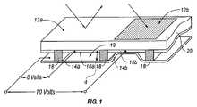
- FIG. 1is an isometric view depicting a portion of one embodiment of an interferometric modulator display in which a movable reflective layer of a first interferometric modulator is in a relaxed position and a movable reflective layer of a second interferometric modulator is in an actuated position.
- FIG. 2is a system block diagram illustrating one embodiment of an electronic device incorporating a 3 ⁇ 3 interferometric modulator display.
- FIG. 3is a diagram of movable mirror position versus applied voltage for one exemplary embodiment of an interferometric modulator of FIG. 1 .
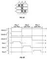
- FIG. 4is an illustration of a set of row and column voltages that may be used to drive an interferometric modulator display.
- FIGS. 5A and 5Billustrate one exemplary timing diagram for row and column signals that may be used to write a frame of display data to the 3 ⁇ 3 interferometric modulator display of FIG. 2 .
- FIGS. 6A and 6Bare system block diagrams illustrating an embodiment of a visual display device comprising a plurality of interferometric modulators.
- FIG. 7Ais a cross section of the device of FIG. 1 .
- FIG. 7Bis a cross section of an alternative embodiment of an interferometric modulator.
- FIG. 7Cis a cross section of another alternative embodiment of an interferometric modulator.
- FIG. 7Dis a cross section of yet another alternative embodiment of an interferometric modulator.
- FIG. 7Eis a cross section of an additional alternative embodiment of an interferometric modulator.
- FIG. 8is a graphical diagram that illustrates the spectral response of an exemplary display that includes the interferometric modulator viewed through a wavelength filter.
- FIG. 9is a graphical diagram that illustrates the spectral response of another exemplary display that includes the interferometric modulator 12 viewed through a wavelength filter.
- FIG. 10a side cross-sectional view of an exemplary wavelength filter.
- FIG. 11a side cross-sectional view of an exemplary display that includes interferometric modulator comprising a wavelength filter.
- interferometric modulator displayswhich include a fixed interferometric wavelength filter or color filter.
- one embodimentincludes a display element comprising a movable reflector positioned at a distance from a first partial reflector to define a first optical cavity that forms an interferometric modulator.
- a second partial reflectoris positioned at a distance from the first partial reflector to define a second optical cavity.
- the first and second partial reflectorsdefine a wavelength filter that produces a spectral response different from that of the interferometric modulator alone.
- the structure so definedprovides additional control over the spectral response of the device while adding only a few additional layers to the display.
- the additional layersmay be formed of the same materials as the other layers of the interferometric modulator so as to further reduce manufacturing complexity.
- the inventioncan be embodied in a multitude of different ways.
- the embodimentsmay be implemented in any device that is configured to display an image, whether in motion (e.g., video) or stationary (e.g., still image), and whether textual or pictorial.
- the embodimentsmay be implemented in or associated with a variety of electronic devices such as, but not limited to, mobile telephones, wireless devices, personal data assistants (PDAs), hand-held or portable computers, GPS receivers/navigators, cameras, MP3 players, camcorders, game consoles, wrist watches, clocks, calculators, television monitors, flat panel displays, computer monitors, auto displays (e.g., odometer display, etc.), cockpit controls and/or displays, display of camera views (e.g., display of a rear view camera in a vehicle), electronic photographs, electronic billboards or signs, projectors, architectural structures, packaging, and aesthetic structures (e.g., display of images on a piece of jewelry).
- MEMS devices of similar structure to those described hereincan also be used in non-display applications such as in electronic switching devices.
- FIG. 1One interferometric modulator display embodiment comprising an interferometric MEMS display element is illustrated in FIG. 1 .
- the pixelsare in either a bright or dark state.
- the display elementIn the bright (“on” or “open”) state, the display element reflects a large portion of incident visible light to a user.
- the dark (“off” or “closed”) stateWhen in the dark (“off” or “closed”) state, the display element reflects little incident visible light to the user.
- the light reflectance properties of the “on” and “off” statesmay be reversed.
- MEMS pixelscan be configured to reflect predominantly at selected colors, allowing for a color display in addition to black and white.
- FIG. 1is an isometric view depicting two adjacent pixels in a series of pixels of a visual display, wherein each pixel comprises a MEMS interferometric modulator.
- an interferometric modulator displaycomprises a row/column array of these interferometric modulators.
- Each interferometric modulatorincludes a pair of reflective layers positioned at a variable and controllable distance from each other to form a resonant optical cavity with at least one variable dimension.
- one of the reflective layersmay be moved between two positions. In the first position, referred to herein as the relaxed position, the movable reflective layer is positioned at a relatively large distance from a fixed partially reflective layer.
- the movable reflective layerIn the second position, referred to herein as the actuated position, the movable reflective layer is positioned more closely adjacent to the partially reflective layer. Incident light that reflects from the two layers interferes constructively or destructively depending on the position of the movable reflective layer, producing either an overall reflective or non-reflective state for each pixel.
- the depicted portion of the pixel array in FIG. 1includes two adjacent interferometric modulators 12 a and 12 b .
- a movable reflective layer 14 ais illustrated in a relaxed position at a predetermined distance from an optical stack 16 a , which includes a partially reflective layer.
- the movable reflective layer 14 bis illustrated in an actuated position adjacent to the optical stack 16 b.
- optical stack 16typically comprise of several fused layers, which can include an electrode layer, such as indium tin oxide (ITO), a partially reflective layer, such as chromium, and a transparent dielectric.
- ITOindium tin oxide
- the optical stack 16is thus electrically conductive, partially transparent and partially reflective, and may be fabricated, for example, by depositing one or more of the above layers onto a transparent substrate 20 .
- the layersare patterned into parallel strips, and may form row electrodes in a display device as described further below.
- the movable reflective layers 14 a , 14 bmay be formed as a series of parallel strips of a deposited metal layer or layers (orthogonal to the row electrodes of 16 a , 16 b ) deposited on top of posts 18 and an intervening sacrificial material deposited between the posts 18 . When the sacrificial material is etched away, the movable reflective layers 14 a , 14 b are separated from the optical stacks 16 a , 16 b by a defined gap 19 .
- a highly conductive and reflective materialsuch as aluminum may be used for the reflective layers 14 , and these strips may form column electrodes in a display device.
- the cavity 19remains between the movable reflective layer 14 a and optical stack 16 a , with the movable reflective layer 14 a in a mechanically relaxed state, as illustrated by the pixel 12 a in FIG. 1 .
- a potential differenceis applied to a selected row and column, the capacitor formed at the intersection of the row and column electrodes at the corresponding pixel becomes charged, and electrostatic forces pull the electrodes together.
- the movable reflective layer 14is deformed and is forced against the optical stack 16 .
- a dielectric layerwithin the optical stack 16 may prevent shorting and control the separation distance between layers 14 and 16 , as illustrated by pixel 12 b on the right in FIG. 1 .
- the behavioris the same regardless of the polarity of the applied potential difference. In this way, row/column actuation that can control the reflective vs. non-reflective pixel states is analogous in many ways to that used in conventional LCD and other display technologies.
- FIGS. 2 through 5illustrate one exemplary process and system for using an array of interferometric modulators in a display application.
- FIG. 2is a system block diagram illustrating one embodiment of an electronic device that may incorporate aspects of the invention.
- the electronic deviceincludes a processor 21 which may be any general purpose single- or multi-chip microprocessor such as an ARM, Pentium®, Pentium II®, Pentium III®, Pentium IV®, Pentium® Pro, an 8051, a MIPS®, a Power PC®, an ALPHA®, or any special purpose microprocessor such as a digital signal processor, microcontroller, or a programmable gate array.
- the processor 21may be configured to execute one or more software modules.
- the processormay be configured to execute one or more software applications, including a web browser, a telephone application, an email program, or any other software application.
- the processor 21is also configured to communicate with an array driver 22 .
- the array driver 22includes a row driver circuit 24 and a column driver circuit 26 that provide signals to a display array or panel 30 .
- the cross section of the array illustrated in FIG. 1is shown by the lines 1 - 1 in FIG. 2 .
- the row/column actuation protocolmay take advantage of a hysteresis property of these devices illustrated in FIG. 3 . It may require, for example, a 10 volt potential difference to cause a movable layer to deform from the relaxed state to the actuated state. However, when the voltage is reduced from that value, the movable layer maintains its state as the voltage drops back below 10 volts.
- the movable layerdoes not relax completely until the voltage drops below 2 volts.
- There is thus a range of voltage, about 3 to 7 V in the example illustrated in FIG. 3where there exists a window of applied voltage within which the device is stable in either the relaxed or actuated state. This is referred to herein as the “hysteresis window” or “stability window.”
- hysteresis windowor “stability window.”
- the row/column actuation protocolcan be designed such that during row strobing, pixels in the strobed row that are to be actuated are exposed to a voltage difference of about 10 volts, and pixels that are to be relaxed are exposed to a voltage difference of close to zero volts. After the strobe, the pixels are exposed to a steady state voltage difference of about 5 volts such that they remain in whatever state the row strobe put them in. After being written, each pixel sees a potential difference within the “stability window” of 3-7 volts in this example. This feature makes the pixel design illustrated in FIG. 1 stable under the same applied voltage conditions in either an actuated or relaxed pre-existing state.
- each pixel of the interferometric modulatoris essentially a capacitor formed by the fixed and moving reflective layers, this stable state can be held at a voltage within the hysteresis window with almost no power dissipation. Essentially no current flows into the pixel if the applied potential is fixed.
- a display framemay be created by asserting the set of column electrodes in accordance with the desired set of actuated pixels in the first row.
- a row pulseis then applied to the row 1 electrode, actuating the pixels corresponding to the asserted column lines.
- the asserted set of column electrodesis then changed to correspond to the desired set of actuated pixels in the second row.
- a pulseis then applied to the row 2 electrode, actuating the appropriate pixels in row 2 in accordance with the asserted column electrodes.
- the row 1 pixelsare unaffected by the row 2 pulse, and remain in the state they were set to during the row 1 pulse. This may be repeated for the entire series of rows in a sequential fashion to produce the frame.
- the framesare refreshed and/or updated with new display data by continually repeating this process at some desired number of frames per second.
- protocols for driving row and column electrodes of pixel arrays to produce display framesare also well known and may be used in conjunction with the present invention.
- FIGS. 4 and 5illustrate one possible actuation protocol for creating a display frame on the 3 ⁇ 3 array of FIG. 2 .
- FIG. 4illustrates a possible set of column and row voltage levels that may be used for pixels exhibiting the hysteresis curves of FIG. 3 .
- actuating a pixelinvolves setting the appropriate column to ⁇ V bias , and the appropriate row to + ⁇ V, which may correspond to ⁇ 5 volts and +5 volts respectively Relaxing the pixel is accomplished by setting the appropriate column to +V bias , and the appropriate row to the same + ⁇ V, producing a zero volt potential difference across the pixel.
- the pixelsare stable in whatever state they were originally in, regardless of whether the column is at +V bias , or ⁇ V bias .
- voltages of opposite polarity than those described abovecan be used, e.g., actuating a pixel can involve setting the appropriate column to +V bias , and the appropriate row to ⁇ V.
- releasing the pixelis accomplished by setting the appropriate column to ⁇ V bias , and the appropriate row to the same ⁇ V, producing a zero volt potential difference across the pixel.
- FIG. 5Bis a timing diagram showing a series of row and column signals applied to the 3 ⁇ 3 array of FIG. 2 which will result in the display arrangement illustrated in FIG. 5A , where actuated pixels are non-reflective.
- the pixelsPrior to writing the frame illustrated in FIG. 5A , the pixels can be in any state, and in this example, all the rows are at 0 volts, and all the columns are at +5 volts. With these applied voltages, all pixels are stable in their existing actuated or relaxed states.
- pixels ( 1 , 1 ), ( 1 , 2 ), ( 2 , 2 ), ( 3 , 2 ) and ( 3 , 3 )are actuated.
- columns 1 and 2are set to ⁇ 5 volts
- column 3is set to +5 volts. This does not change the state of any pixels, because all the pixels remain in the 3-7 volt stability window.
- Row 1is then strobed with a pulse that goes from 0, up to 5 volts, and back to zero. This actuates the ( 1 , 1 ) and ( 1 , 2 ) pixels and relaxes the ( 1 , 3 ) pixel. No other pixels in the array are affected.
- row 2is set to ⁇ 5 volts, and columns 1 and 3 are set to +5 volts.
- the same strobe applied to row 2will then actuate pixel ( 2 , 2 ) and relax pixels ( 2 , 1 ) and ( 2 , 3 ). Again, no other pixels of the array are affected.
- Row 3is similarly set by setting columns 2 and 3 to ⁇ 5 volts, and column 1 to +5 volts.
- the row 3strobe sets the row 3 pixels as shown in FIG. 5A . After writing the frame, the row potentials are zero, and the column potentials can remain at either +5 or ⁇ 5 volts, and the display is then stable in the arrangement of FIG. 5A .
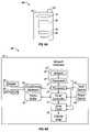
- FIGS. 6A and 6Bare system block diagrams illustrating an embodiment of a display device 40 .
- the display device 40can be, for example, a cellular or mobile telephone.
- the same components of display device 40 or slight variations thereofare also illustrative of various types of display devices such as televisions and portable media players.
- the display device 40includes a housing 41 , a display 30 , an antenna 43 , a speaker 44 , an input device 48 , and a microphone 46 .
- the housing 41is generally formed from any of a variety of manufacturing processes as are well known to those of skill in the art, including injection molding, and vacuum forming.
- the housing 41may be made from any of a variety of materials, including but not limited to plastic, metal, glass, rubber, and ceramic, or a combination thereof.
- the housing 41includes removable portions (not shown) that may be interchanged with other removable portions of different color, or containing different logos, pictures, or symbols.
- the display 30 of exemplary display device 40may be any of a variety of displays, including a bi-stable display, as described herein.
- the display 30includes a flat-panel display, such as plasma, EL, OLED, STN LCD, or TFT LCD as described above, or a non-flat-panel display, such as a CRT or other tube device, as is well known to those of skill in the art.
- the display 30includes an interferometric modulator display, as described herein.
- the components of one embodiment of exemplary display device 40are schematically illustrated in FIG. 6B .
- the illustrated exemplary display device 40includes a housing 41 and can include additional components at least partially enclosed therein.
- the exemplary display device 40includes a network interface 27 that includes an antenna 43 which is coupled to a transceiver 47 .
- the transceiver 47is connected to a processor 21 , which is connected to conditioning hardware 52 .
- the conditioning hardware 52may be configured to condition a signal (e.g. filter a signal).
- the conditioning hardware 52is connected to a speaker 45 and a microphone 46 .
- the processor 21is also connected to an input device 48 and a driver controller 29 .
- the driver controller 29is coupled to a frame buffer 28 , and to an array driver 22 , which in turn is coupled to a display array 30 .
- a power supply 50provides power to all components as required by the particular exemplary display device 40 design.
- the network interface 27includes the antenna 43 and the transceiver 47 so that the exemplary display device 40 can communicate with one ore more devices over a network. In one embodiment the network interface 27 may also have some processing capabilities to relieve requirements of the processor 21 .
- the antenna 43is any antenna known to those of skill in the art for transmitting and receiving signals. In one embodiment, the antenna transmits and receives RF signals according to the IEEE 802.11 standard, including IEEE 802.11(a), (b), or (g). In another embodiment, the antenna transmits and receives RF signals according to the BLUETOOTH standard. In the case of a cellular telephone, the antenna is designed to receive CDMA, GSM, AMPS or other known signals that are used to communicate within a wireless cell phone network.
- the transceiver 47pre-processes the signals received from the antenna 43 so that they may be received by and further manipulated by the processor 21 .
- the transceiver 47also processes signals received from the processor 21 so that they may be transmitted from the exemplary display device 40 via the antenna 43 .
- the transceiver 47can be replaced by a receiver.
- network interface 27can be replaced by an image source, which can store or generate image data to be sent to the processor 21 .
- the image sourcecan be a digital video disc (DVD) or a hard-disc drive that contains image data, or a software module that generates image data.
- Processor 21generally controls the overall operation of the exemplary display device 40 .
- the processor 21receives data, such as compressed image data from the network interface 27 or an image source, and processes the data into raw image data or into a format that is readily processed into raw image data.
- the processor 21then sends the processed data to the driver controller 29 or to frame buffer 28 for storage.
- Raw datatypically refers to the information that identifies the image characteristics at each location within an image. For example, such image characteristics can include color, saturation, and gray-scale level.
- the processor 21includes a microcontroller, CPU, or logic unit to control operation of the exemplary display device 40 .
- Conditioning hardware 52generally includes amplifiers and filters for transmitting signals to the speaker 45 , and for receiving signals from the microphone 46 .
- Conditioning hardware 52may be discrete components within the exemplary display device 40 , or may be incorporated within the processor 21 or other components.
- the driver controller 29takes the raw image data generated by the processor 21 either directly from the processor 21 or from the frame buffer 28 and reformats the raw image data appropriately for high speed transmission to the array driver 22 . Specifically, the driver controller 29 reformats the raw image data into a data flow having a raster-like format, such that it has a time order suitable for scanning across the display array 30 . Then the driver controller 29 sends the formatted information to the array driver 22 .
- a driver controller 29such as a LCD controller, is often associated with the system processor 21 as a stand-alone Integrated Circuit (IC), such controllers may be implemented in many ways. They may be embedded in the processor 21 as hardware, embedded in the processor 21 as software, or fully integrated in hardware with the array driver 22 .
- the array driver 22receives the formatted information from the driver controller 29 and reformats the video data into a parallel set of waveforms that are applied many times per second to the hundreds and sometimes thousands of leads coming from the display's x-y matrix of pixels.
- driver controller 29is a conventional display controller or a bi-stable display controller (e.g., an interferometric modulator controller).
- array driver 22is a conventional driver or a bi-stable display driver (e.g., an interferometric modulator display).
- a driver controller 29is integrated with the array driver 22 .
- display array 30is a typical display array or a bi-stable display array (e.g., a display including an array of interferometric modulators).
- the input device 48allows a user to control the operation of the exemplary display device 40 .
- input device 48includes a keypad, such as a QWERTY keyboard or a telephone keypad, a button, a switch, a touch-sensitive screen, a pressure- or heat-sensitive membrane.
- the microphone 46is an input device for the exemplary display device 40 . When the microphone 46 is used to input data to the device, voice commands may be provided by a user for controlling operations of the exemplary display device 40 .
- Power supply 50can include a variety of energy storage devices as are well known in the art.
- power supply 50is a rechargeable battery, such as a nickel-cadmium battery or a lithium ion battery.
- power supply 50is a renewable energy source, a capacitor, or a solar cell, including a plastic solar cell, and solar-cell paint.
- power supply 50is configured to receive power from a wall outlet.
- control programmabilityresides, as described above, in a driver controller which can be located in several places in the electronic display system. In some cases control programmability resides in the array driver 22 . Those of skill in the art will recognize that the above-described optimization may be implemented in any number of hardware and/or software components and in various configurations.
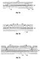
- FIGS. 7A-7Eillustrate five different embodiments of the movable reflective layer 14 and its supporting structures.
- FIG. 7Ais a cross section of the embodiment of FIG. 1 , where a strip of metal material 14 is deposited on orthogonally extending supports 18 .
- FIG. 7Bthe moveable reflective layer 14 is attached to supports at the corners only, on tethers 32 .
- FIG. 7Cthe moveable reflective layer 14 is suspended from a deformable layer 34 , which may comprise a flexible metal.
- the deformable layer 34connects, directly or indirectly, to the substrate 20 around the perimeter of the deformable layer 34 .
- connection postsare herein referred to as support posts.
- the embodiment illustrated in FIG. 7Dhas support post plugs 42 upon which the deformable layer 34 rests.
- the movable reflective layer 14remains suspended over the cavity, as in FIGS. 7A-7C , but the deformable layer 34 does not form the support posts by filling holes between the deformable layer 34 and the optical stack 16 . Rather, the support posts are formed of a planarization material, which is used to form support post plugs 42 .
- the embodiment illustrated in FIG. 7Eis based on the embodiment shown in FIG. 7D , but may also be adapted to work with any of the embodiments illustrated in FIGS. 7A-7C as well as additional embodiments not shown. In the embodiment shown in FIG. 7E , an extra layer of metal or other conductive material has been used to form a bus structure 44 . This allows signal routing along the back of the interferometric modulators, eliminating a number of electrodes that may otherwise have had to be formed on the substrate 20 .
- the interferometric modulatorsfunction as direct-view devices, in which images are viewed from the front side of the transparent substrate 20 , the side opposite to that upon which the modulator is arranged.
- the reflective layer 14optically shields the portions of the interferometric modulator on the side of the reflective layer opposite the substrate 20 , including the deformable layer 34 and the bus structure 44 . This allows the shielded areas to be configured and operated upon without negatively affecting the image quality.
- This separable modulator architectureallows the structural design and materials used for the electromechanical aspects and the optical aspects of the modulator to be selected and to function independently of each other.
- the modulator 12(i.e., both modulators 12 a and 12 b ) includes an optical cavity formed between the mirrors 14 (i.e., mirrors 14 a and 14 b ) and 16 (mirrors 16 a and 16 b , respectively).
- the characteristic distance, or effective optical path length, d, of the optical cavitydetermines the resonant wavelengths, ⁇ , of the optical cavity and thus of the interferometric modulator 12 .
- a peak resonant visible wavelength, ⁇ , of the interferometric modulator 12generally corresponds to the perceived color of light reflected by the modulator 12 .
- the optical path length dis equal to 1 ⁇ 2 N ⁇ , where N is an integer.
- the integer Nmay be referred to as the order of interference of the reflected light.
- the order of a modulator 12also refers to the order N of light reflected by the modulator 12 when the mirror 14 is in at least one position.
- a first order red interferometric modulator 12may have an optical path length d of about 325 nm, corresponding to a wavelength ⁇ of about 650 nm. Accordingly, a second order red interferometric modulator 12 may have an optical path length d of about 650 nm.
- the optical path length, dis substantially equal to the distance between the reflective layers that form the optical cavity of the interferometric modulators.
- the space between the reflective layerscomprises only a gas (e.g., air) having an index of refraction of approximately 1
- the effective optical path lengthis substantially equal to the distance between the reflective layers.
- a layer of dielectric material in the optical pathtypically have an index of refraction greater than one.
- the optical cavityis formed to have the desired optical path length d by selecting both the distance between the reflective layers and the thickness and index of refraction of the dielectric layer, or of any other layers between the reflective layers.
- the optical path length dis equal to d 1 n 1 +d 2 n 2 , where d 1 is the thickness of dielectric layer, n 1 is the index of refraction of the dielectric layer and similarly d 2 is the thickness of air gap and n 2 is the index of refraction of the air gap.
- the movable reflective layerin the actuated position, is sufficiently close to the fixed reflective layer, and the optical path length, d, accounting for any dielectric layers, is thus sufficiently small, that the effects of interference are negligible.
- the modulator 12therefore acts as a mirror that reflects substantially all colors of incident visible light substantially equally, e.g., as white light.
- the broadband mirror effectis caused because the small optical path length d is too small for optical resonance in the visible band.
- the reflective layer 14 in such an embodimentthus merely acts as a reflective surface with respect to visible light.
- modulators 12reflect light that has one or more spectral peaks when wavelength is plotted versus intensity.
- the perceived color of light produced by a modulator 12depends on the number, location, and spectral width of these peaks of the modulator 12 within the visible spectrum.
- the width of such peaksmay be characterized by the width of the peak at the half maximum of intensity of reflected light, e.g., the full width at half maximum.
- higher order modulators 12reflect light over a narrower range of wavelengths, e.g., have a narrower peak or higher “Q” value, and thus produce colored light that is more saturated.
- the saturation of the modulators 12 that comprise a color pixelaffects properties of a display such as the color gamut and white point of the display.
- the second order modulator 12may be selected to have a different central peak optical wavelength.
- the modulators 12may be formed so as to increase the color saturation of reflected light.
- Saturationrefers to the narrowness of the range of wavelengths of light output. A highly saturated hue has a vivid, intense color, while a less saturated hue appears more muted and grey.
- a laserwhich produces a very narrow range of wavelengths, produces highly saturated light.
- a typical incandescent light bulbproduces white light that may have a desaturated red or blue color.
- the modulator 12is formed with an optical path length, d, corresponding to higher order of interference, e.g., 2nd or 3rd order, to increase the saturation of reflected color light.
- each pixelincludes one or more color modulators 12 , e.g., modulators configured to reflect red, green, and blue light, and one or more “white” modulators 12 configured to reflect white light.
- color modulators 12e.g., modulators configured to reflect red, green, and blue light
- white modulators 12configured to reflect white light.
- light from the red, green, and/or blue modulators 12 in their reflective statescombines to output colored light.
- Light from the white modulators 12can be used to output white or gray light. Use of white in combination with color may increase the brightness or intensity of the pixels.
- the white point of a displayis the hue that is considered to be generally neutral (gray or achromatic).
- the white point of a display devicemay be characterized based on a comparison of white light produced by the device with the spectral content of light emitted by a black body at a particular temperature (“black body radiation”).
- black body radiationis an idealized object that absorbs all light incident upon the object and which reemits the light with a spectrum dependent on the temperature of the black body.
- the black body spectrum at 6,500° Kmay be referred to as white light having a color temperature of 6,500° K
- Such color temperatures, or white points of approximately 5,000°-10,000° Kare generally identified with daylight.
- CIEInternational Commission on Illumination
- light source designations of “d”refer to daylight.
- standard white points D 55 , D 65 , and D 75which correlate with color temperatures of 5,500° K, 6,500° K, and 7,500° K, are standard daylight white points.
- a display devicemay be characterized by the white point of the white light produced by a display.
- human perception of a displayis at least partially determined by the perception of white light from the display.
- a display or light source having a lower white pointe.g., D55
- a display having a higher temperature white pointe.g., D75
- Usersgenerally respond more favorably to displays having higher temperature white points.
- controlling the white point of a displaydesirably provides some control over a viewer's response to a display.
- Embodiments of the interferometric modulator array 30may be configured to produce white light in which the white point is selected to conform to a standardized white point under one or more anticipated lighting conditions.
- White lightcan be produced by the pixel array 30 by including one or more interferometric modulators 12 for each pixel.
- the pixel array 30includes pixels of groups of red, green, and blue interferometric modulators 12 .
- the balance, or relative proportions, of the colors produced by each pixel in the pixel array 30may be further affected by the relative reflective areas of each of the interferometric modulators 12 , e.g., of the red, green, and blue interferometric modulators 12 .
- the white point of reflected light from the pixel array 30 of interferometric modulators 12is generally dependent on the spectral characteristics of incident light.
- the white point of reflected lightmay be configured to be different than the white point of incident light.
- the pixel array 30may be configured to reflect D75 light when used in D65 sunlight.
- the distances d and areas of the interferometric modulators 12 in the pixel array 30are selected so that white light produced by the pixel array 30 corresponds to a particular standardized white point in an anticipated lighting condition, e.g., in sunlight, under fluorescent light, or from a front light positioned to illuminate the pixel array 30 .
- the white point of the pixel array 30may be selected to be D 55 , D 65 , or D 75 in particular lighting conditions.
- the light reflected by the pixel array 30may have a different white point than the light of an anticipated or configured light source.
- a particular pixel array 30may be configured to reflect D75 light when viewed under D65 sunlight.
- the white point of a displaymay be selected with reference to a source of illumination configured with the display, e.g., a front light, or with reference to a particular viewing condition.
- a displaymay be configured to have a selected white point, e.g., D55, D65, or D75, when viewed under anticipated or typical sources of illumination such as incandescent, fluorescent, or natural light sources.
- a display for use in a handheld devicefor example, may be configured to have a selected white point when viewed under sunlight conditions.
- a display for use in an office environmentmay be configured to have a selected white point, e.g., D75, when illuminated by typical office fluorescent lights.
- different distances d and areas of modulators 12may be selected to produce other standardized white point settings for different viewing environments.
- the red, green, and blue modulators 12may also be controlled so as to be in reflective or non-reflective states for different amounts of time so as to further vary the relative balance of reflected red, green, and blue light, and thus the white point of reflected light.
- the ratio of reflective areas of each of the color modulators 12may be selected so as to control the white point in different viewing environments.
- the optical path length dmay be selected so as to correspond to a common multiple of more than one visible resonant wavelength, e.g., first, second, or third order peaks of red, green, and blue, so that the interferometric modulator 12 reflects white light characterized by three visible peaks in its spectral response.
- the optical path length dmay be selected so that the white light produced corresponds to a standardized white point.
- An exemplary color displayincludes red, green, and blue display elements. Other colors are produced in such a display by varying the relative intensity of light produced by the red, green, and blue elements. Such mixtures of primary colors such as red, green, and blue are perceived by the human eye as other colors.
- the relative values of red, green, and blue in such a color systemmay be referred to as tristimulus values in reference to the stimulation of red, green, and blue light sensitive portions of the human eye.
- the range of colors that can be produced by a particular displaymay be referred to as the color gamut of the display. In general, increasing the saturation of the primary colors increases the color gamut, or range of colors that can be produced by the display. While an exemplary color system based on red, green, and blue are disclosed herein, in other embodiments, the display may include modulators 12 having sets of colors that define other color systems in terms of sets of primary colors other than red, green, and blue.
- an output spectral peak of a light modulator that is broad or widewill appear brighter than one that is narrow.
- the broader spectrumwill appear brighter, it will also appear pastel in color, i.e., less saturated.
- the saturation of light output by a display that includes the interferometric modulator 12is increased using a color filter.
- a displaymay include a color filter that is configured to output light having a wavelength response peak that is narrower than the visible light wavelength response peak of the modulator 12 .
- Embodimentsmay also reduce viewing angle dependent color shift of the display because a source of the light is at a predetermined and consistent position and distance relative to the reflectors 14 and 16 of the modulator 12 . Thus, if there is any color shift due to the position of the light source relative to the modulators 12 , the interferometric modulator 12 can be tuned to reduce or eliminate this color shift.
- FIG. 8is a graphical diagram that illustrates the spectral response of an exemplary display that includes the interferometric modulator 12 viewed through a wavelength filter.
- the vertical axisrepresents the total fraction of optical intensity of light incident on the interferometric modulator that is reflected by the interferometric modulator or transmitted by the wavelength filter when illuminated by white light.
- a trace 82illustrates the spectral response of the interferometric modulator 12 when viewed without the wavelength filter.
- a trace 84illustrates the spectral response of the wavelength filter in isolation.
- a trace 86illustrates the spectral response of reflected light of an embodiment of a display that includes the wavelength filter and the interferometric modulator 12 .
- the trace 82includes a single peak in the visible spectrum.
- the trace 84includes a single peak in the visible spectrum that is narrower in width, and somewhat centered within the peak defined by the trace 82 .
- the peak spectral response of the interferometric modulator 12is substantially narrowed.
- the peak response of the combined optical system of the wavelength filter and the interferometric modulatoris reduced to be similar in width to the width of the peak of the wavelength filter, which is substantially smaller than the width of the peak spectral response of the modulator 12 in isolation.
- the narrower peaked response of the displayprovides more saturated colors and an improved color gamut. The color gamut of the display may thus be adjusted without modifying the spectral response of the interferometric modulators 12 .
- FIG. 9is a graphical diagram that illustrates the spectral response of another exemplary display that includes the interferometric modulator 12 viewed through a wavelength filter.
- the vertical axisrepresents the total fraction of optical intensity of light incident on the interferometric modulator that is reflected by the interferometric modulator or transmitted by the wavelength filter.
- a trace 82illustrates the spectral response of the interferometric modulator 12 when viewed without the wavelength filter.
- a trace 88illustrates the spectral response of the wavelength filter in isolation.
- a trace 92illustrates the spectral response of reflected light of an embodiment of a display that includes the wavelength filter and the interferometric modulator 12 .
- the trace 82includes a single peak in the visible spectrum.
- the trace 88includes a single peak in the visible spectrum that is narrower in width, and which does not completely overlaps the peak defined by the trace 82 , rather than being within the peak defined by the trace 82 as in FIG. 8 .
- the peak spectral response of the interferometric modulator 12is even more narrowed than the peak system response illustrated by the trace 86 of FIG. 8 .
- the peak response of the combined optical system of the wavelength filter and the interferometric modulatoris narrower than even the peak of the wavelength filter.
- the wavelength filter with a spectral peak that does not completely overlap the peak spectral response of the interferometric modulatorthus provides even more saturated colors than using a filter with the spectral properties illustrated in FIG. 8 .
- the spectral response of the combined optical system formed by the wavelength filter and the interferometric modulator 12has a central peak spectral response that is shifted to be between the separate peak responses of the filter and interferometric modulator 12 .
- Such a filtermay thus be employed to adjust both the saturation and the hue of the display by both narrowing and shifting the spectral profile of the spectral response of the system illustrated by the trace 92 relative to the spectral response of the modulator 12 as illustrated by the trace 82 .
- FIG. 10is a side cross-sectional view of an exemplary wavelength filter 100 having a spectral response such as illustrated by traces like the traces 84 and 88 in FIG. 8 or 9 , respectively.
- the filter 100comprises a thin film structure 101 that serves as an interference-based wavelength (color) filter.
- the thin film structure 101comprises a first partially reflective layer 102 , a first dielectric layer 104 , a second partially reflective layer 106 , a second dielectric layer 108 , a third partially reflective layer 110 and a substrate 114 .
- the partially reflective layers 102 , 106 , 110may comprise metal and thus be optical absorbing layers.
- the thin film structure 101is applied as continuous coatings to the substrate 114 . That is because, in this embodiment, there is no movable mirror within the thin film structure 101 .
- the substrate 114may include a layer of SiO 2 , glass, plastic or any other suitable material that permits light to pass therethrough.
- the partially reflective layers 102may comprise the same material or different materials.
- one or more of the partially reflective layers 102 , 106 , 110comprise a metal.
- the partially reflective layersmay comprise a metal selected from the group consisting of chromium, titanium, molybdenum, gold and indium tin oxide (ITO).
- the partially reflective layerscomprise chromium.
- the partially reflective layercomprises a material other than metal, such as silicon nitride.
- the first dielectric 104 and second dielectric 108may also be the same material or different materials.
- at least one of the first and second dielectric 104 , 108are transparent oxides.
- at least one of the first and second oxides 104 , 108comprises SiO 2 .
- the optical density of the filtercan be varied by varying the thickness of the partially reflective layer 106 , which as described above, may comprise metal.
- the partial reflectorcomprises aluminum.
- other suitable materials with reflective propertiesmay also be utilized.
- the partially reflective layers 102 , 106 , 110may comprise nanolaminate structures.
- the first and third partially reflective layers 102 , 110 and the two oxide layers 104 , 108are the same thickness, such that reflected light would be similar in both halves of the structure.
- the structure 101is asymmetric to influence the relationship between reflected color and transmitted color.
- the layerscan be used on plastic substrates as well as glass substrates.
- the filtersmay be coated with a transparent polymer coating in order to prevent scratches.
- the thickness and composition of the thin films in the wavelength filters described abovecan be adjusted to modulate the properties of the filters.
- the thickness and index of refraction of the dielectric layerscan be adjusted such that the thin film stack is a color filter.
- the thickness and composition of the dielectric layersare selected such that the layers form a magenta filter.
- the thickness and composition of the dielectric layersare selected such that the structure serves as a red, green or blue band pass filter.
- the appropriate materials and thicknesses of the dielectric layersmay be selected to produce a filter with the desired properties in a manner similar to discussed above for configuring the interferometric modulator 12 ,
- Other techniquessuch as for example, known techniques disclosed in the “American Institute Physics Handbook,” 6-172 (3rd. ed. 1972) may also be used.
- designsmay also be obtained in other ways.
- Wavelength filters based on interferometric modulator structures as described abovemay be used in a wide range of applications for which wavelength or color filters are typically utilized.
- optical devicessuch as microscopes, binoculars, telescopes, and sunglasses may include such filters.
- the wavelength filter 101is utilized as a coating on the lenses in sunglasses.
- the color of the glassescould be either a broadband reflector or an iridescent reflector.
- the thin film structureis an interference based filter, the observed color of an object would shift with viewing angle.
- the reflected color on each side of the lenscan be selected.
- the color seen by the wearer and the color seen by viewers of the outside of the sunglassescan be adjusted to create a desired effect.
- the thin film structure 101 illustrated in FIG. 10is utilized as a coating on sunglass lenses.
- the thickness and composition of the dielectric layer 104is adjusted such that the sunglass lenses appear colored to the external viewer.
- FIG. 11is a side cross-sectional view of an exemplary interferometric modulator 122 that includes a wavelength filter.
- the modulator 122includes the thin film wavelength filter as part of an optical stack 126 formed on the substrate 20 .
- the optical stack 126includes a partially reflective layer 102 , a transparent dielectric layer 104 , a transparent electrode 124 , a partially reflective layer 106 , and a dielectric layer 108 .
- the optical stack 126is positioned with respect to the reflective layer 14 so as to define a cavity region in which the reflective layer 14 may move upon deflection.
- the reflective layer 14is connected to the substrate 20 by the posts 18 .
- the modulator 122may include features according to any embodiment of the modulator 12 disclosed herein.
- the dielectric layer 104 and partially reflective layers 102 and 106together define an optical cavity that form an interferometric wavelength filter.
- the thickness and composition (index of refraction) of the dielectric layer 104can be adjusted to vary the effective optical path length of the optical cavity formed between layers 102 and 106 to produce the desired color filter.
- the dielectric materialmay be selected such that a magenta filter is produced. If the interferometric device is set up to produce green light (in the absence of a wavelength filter), the magenta filter will adjust the wavelength of output light such that it appears white to the viewer.
- the dielectric layeris adjusted to form a red, green or blue band pass filters as desired. Such filters only allow the desired wavelength of light to pass into and out of the device. As noted with reference to FIGS. 8 and 9 , such wavelength filters may employed to increase the saturation of colored light produced by the modulator 12 and thereby increase the color gamut of a display including the modulator 12 comprising the optical stack 126 .
- one embodimentincludes modulators 122 in which the optical path length, d, is selected to produce a first order green spectral response.
- the optical stack 126 in such modulators 122is configured to increase the saturation of the green.
- the reflective layer 102may comprise a thin (30 angstroms rather than 50-80 angstroms) chrome layer.
- the optical stack 126may be configured to output magenta light when illuminated with white light so that the modulator 122 so construction reflects white light.
- an interferometric modulator device incorporating a wavelength filter in the optical stack 126requires only a few additional process steps compared to the production of an interferometric modulator device without the filter.
- incorporation of the wavelength filterrequires only the additional steps of depositing the dielectric layer 104 and the partially reflective layer 102 .
- the additional processing requirementscan be further reduced or minimized if the dielectric layer 104 comprises the same material as the dielectric layer 108 and/or if the partially reflective layer 102 is made of the same material as the partially reflective layer 106 .
- the reflective layer 14 and the reflective layer 106defines a first optical cavity characterized by the optical path, d 1 , therebetween.
- the optical stack 126defines a second optical cavity characterized by an optical path length d 2 between the partially reflective layers 106 and 102 .
- the reflective layer 14 and the partially reflectively 102define a third cavity having the optical path length d 3 therebetween.
- the output of the modulator 12may be further adjusted by selection of the layers of the optical stack 126 and the optical path lengths d 3 so as to select visible light properties of this third cavity. In other embodiments, these parameters may be selected so that the third cavity does not provide any significant contribution to visible light spectral response of the modulator 12 .
- the color of light reflected by the interferometric modulator 122shifts when the modulator 122 is viewed from different angles.
- the color of light reflected from the interferometric modulator 122may vary for different angles of incidence (and reflection) with respect to an axis AA as illustrated in FIG. 11 .
- the peak resonant wavelength of the reflected lightis decreased. The user therefore perceives different colors depending on his or her angle of view.
- this phenomenonis referred to as a “color shift.”
- This color shiftis typically identified with reference to a color produced by an interferometric modulator 12 when viewed along the axis AA.
- the optical stack 126is configured to selectively filter light that “shifted” outside of the desired range of colors for a particular modulator.
- an interferometric modulator 122tends to output light of a reduced intensity at increasing angles as the modulators output is shifted outside of the range of wavelengths transmitted by the wavelength filter.
- an absorptive filtermay be included in the optical stack 126 to filter such light.
- an interference filter in the optical stack 126may be configured to filter such color shifted light.
- the interference filtermay also be subject to such color shift.
- the dielectric layer 104has, in one embodiment, an index of refraction that is larger than that of air in the gap 18 (as shown in FIG. 11 )
- the color shiftis still reduced as compared to the modulator 122 .
- the modulator 122reflects green light and the interference filter portion of the optical stack transmits green light
- the range of green transmitted wavelengthsshifts less than the shift in range of green reflected wavelengths from the modulator.
- the intensity of shifted lightis thereby reduced in aggregate.
- the overall brightness of such a deviceis also reduced, reducing the eye's perception of any change in the hue of output light.
- the interferometric modulator 122can be used in many different embodiments of a display.
- one embodimentincludes the display array 30 comprising interferometric modulators 122 in which the optical path length, d 2 , of the stack 126 is selected to adjust the color balance, or white point of the display array 30 .
- the reflective layers 14 and 106 and the dielectric layer 108are configured so that in the actuated position, the reflective layer 14 comprises a broadband (or white) reflector).
- the layers of the optical stack 126are configured as a color filter so that the modulator 122 outputs colored light.
- the display 30is a color display that includes a plurality of modulators 122 in which the movable reflective layer 14 is configured to be a broadband reflector.
- Such an embodiment of the color display 30produces color by configuring the optical stack 126 in different portions of the display (e.g., different columns) to produce, for example, red, green, and blue light from the modulators 122 .
- Such color displays 30allow the movable reflector (MEMS) portion of the display for each color to be formed to be substantially identical with only the optical stack portion of the color modulators being varied.
- a similar embodimentincludes modulators 122 in which the optical path length, d 1 , is selected to produce multiple peaks in the visible spectrum corresponding to primary colors such as red, green, and blue.
- the optical stack 126 of such modulatorsmay be configured so that portions of the modulators 122 in a particular display 30 output each of the primary colors, e.g., columns of alternating red, green, and blue modulators so as to produce a color display.
- the thickness of dielectric 104may be varied to produce different colors.
- different portions of a display configured to display different colorsmay not have a uniform structure.
- the light modulators for each of the colorsmay be arranged in rows or columns that each have a different stack structure.
Landscapes
- Physics & Mathematics (AREA)
- General Physics & Mathematics (AREA)
- Optics & Photonics (AREA)
- Spectroscopy & Molecular Physics (AREA)
- Engineering & Computer Science (AREA)
- Computer Hardware Design (AREA)
- Theoretical Computer Science (AREA)
- Mechanical Light Control Or Optical Switches (AREA)
- Optical Filters (AREA)
Abstract
Description
Claims (55)
Priority Applications (10)
| Application Number | Priority Date | Filing Date | Title |
|---|---|---|---|
| US11/213,659US7898521B2 (en) | 2004-09-27 | 2005-08-26 | Device and method for wavelength filtering |
| EP05800920AEP1800172B1 (en) | 2004-09-27 | 2005-09-14 | Device and method for wavelength filtering |
| DE602005026418TDE602005026418D1 (en) | 2004-09-27 | 2005-09-14 | DEVICE AND METHOD FOR WAVELENGTH FILTERING |
| AT05800920TATE498854T1 (en) | 2004-09-27 | 2005-09-14 | DEVICE AND METHOD FOR WAVELENGTH FILTERING |
| PCT/US2005/032633WO2006036540A1 (en) | 2004-09-27 | 2005-09-14 | Device and method for wavelength filtering |
| SG200906386-8ASG155974A1 (en) | 2004-09-27 | 2005-09-14 | Device and method for wavelength filtering |
| KR1020077009322AKR101174760B1 (en) | 2004-09-27 | 2005-09-14 | device and method for wavelength filtering |
| CA002580992ACA2580992A1 (en) | 2004-09-27 | 2005-09-14 | Device and method for wavelength filtering |
| TW094133410ATW200619723A (en) | 2004-09-27 | 2005-09-26 | Device and method for wavelength filtering |
| US13/016,107US20110193770A1 (en) | 2004-09-27 | 2011-01-28 | Device and method for wavelength filtering |
Applications Claiming Priority (2)
| Application Number | Priority Date | Filing Date | Title |
|---|---|---|---|
| US61340304P | 2004-09-27 | 2004-09-27 | |
| US11/213,659US7898521B2 (en) | 2004-09-27 | 2005-08-26 | Device and method for wavelength filtering |
Related Child Applications (1)
| Application Number | Title | Priority Date | Filing Date |
|---|---|---|---|
| US13/016,107ContinuationUS20110193770A1 (en) | 2004-09-27 | 2011-01-28 | Device and method for wavelength filtering |
Publications (2)
| Publication Number | Publication Date |
|---|---|
| US20060067633A1 US20060067633A1 (en) | 2006-03-30 |
| US7898521B2true US7898521B2 (en) | 2011-03-01 |
Family
ID=36099188
Family Applications (2)
| Application Number | Title | Priority Date | Filing Date |
|---|---|---|---|
| US11/213,659Expired - Fee RelatedUS7898521B2 (en) | 2004-09-27 | 2005-08-26 | Device and method for wavelength filtering |
| US13/016,107AbandonedUS20110193770A1 (en) | 2004-09-27 | 2011-01-28 | Device and method for wavelength filtering |
Family Applications After (1)
| Application Number | Title | Priority Date | Filing Date |
|---|---|---|---|
| US13/016,107AbandonedUS20110193770A1 (en) | 2004-09-27 | 2011-01-28 | Device and method for wavelength filtering |
Country Status (9)
| Country | Link |
|---|---|
| US (2) | US7898521B2 (en) |
| EP (1) | EP1800172B1 (en) |
| KR (1) | KR101174760B1 (en) |
| AT (1) | ATE498854T1 (en) |
| CA (1) | CA2580992A1 (en) |
| DE (1) | DE602005026418D1 (en) |
| SG (1) | SG155974A1 (en) |
| TW (1) | TW200619723A (en) |
| WO (1) | WO2006036540A1 (en) |
Cited By (28)
| Publication number | Priority date | Publication date | Assignee | Title |
|---|---|---|---|---|
| US20060066641A1 (en)* | 2004-09-27 | 2006-03-30 | Gally Brian J | Method and device for manipulating color in a display |
| US20060066541A1 (en)* | 2004-09-27 | 2006-03-30 | Gally Brian J | Method and device for manipulating color in a display |
| US20060066557A1 (en)* | 2004-09-27 | 2006-03-30 | Floyd Philip D | Method and device for reflective display with time sequential color illumination |
| US20060077149A1 (en)* | 2004-09-27 | 2006-04-13 | Gally Brian J | Method and device for manipulating color in a display |
| US20060077153A1 (en)* | 2004-09-27 | 2006-04-13 | Idc, Llc, A Delaware Limited Liability Company | Reduced capacitance display element |
| US20070132843A1 (en)* | 1994-05-05 | 2007-06-14 | Idc, Llc | Method and system for interferometric modulation in projection or peripheral devices |
| US20080151347A1 (en)* | 2004-02-03 | 2008-06-26 | Idc, Llc | Spatial light modulator with integrated optical compensation structure |
| US20090059346A1 (en)* | 2007-08-29 | 2009-03-05 | Qualcomm Incorporated | Interferometric Optical Modulator With Broadband Reflection Characteristics |
| US20090086301A1 (en)* | 2004-09-27 | 2009-04-02 | Idc, Llc | Display element having filter material diffused in a substrate of the display element |
| US20090219604A1 (en)* | 1999-10-05 | 2009-09-03 | Qualcomm Mems Technologies, Inc. | Photonic mems and structures |
| US20090296191A1 (en)* | 2004-09-27 | 2009-12-03 | Idc, Llc | Method and device for generating white in an interferometric modulator display |
| US20110090136A1 (en)* | 2004-03-06 | 2011-04-21 | Qualcomm Mems Technologies, Inc. | Method and system for color optimization in a display |
| US20110193770A1 (en)* | 2004-09-27 | 2011-08-11 | Qualcomm Mems Technologies, Inc. | Device and method for wavelength filtering |
| US8004743B2 (en) | 2006-04-21 | 2011-08-23 | Qualcomm Mems Technologies, Inc. | Method and apparatus for providing brightness control in an interferometric modulator (IMOD) display |
| US8054528B2 (en) | 2004-09-27 | 2011-11-08 | Qualcomm Mems Technologies Inc. | Display device having an array of spatial light modulators with integrated color filters |
| US20120236042A1 (en)* | 2011-03-15 | 2012-09-20 | Qualcomm Mems Technologies, Inc. | White point tuning for a display |
| US8416154B2 (en) | 2004-09-27 | 2013-04-09 | Qualcomm Mems Technologies, Inc. | Apparatus and method for reducing perceived color shift |
| US8422108B2 (en) | 1995-11-06 | 2013-04-16 | Qualcomm Mems Technologies, Inc. | Method and device for modulating light with optical compensation |
| US8798425B2 (en) | 2007-12-07 | 2014-08-05 | Qualcomm Mems Technologies, Inc. | Decoupled holographic film and diffuser |
| US20140272217A1 (en)* | 2013-03-18 | 2014-09-18 | Apple Inc. | Methods and structures for thermal management in an electronic device |
| US8848294B2 (en) | 2010-05-20 | 2014-09-30 | Qualcomm Mems Technologies, Inc. | Method and structure capable of changing color saturation |
| US8872085B2 (en) | 2006-10-06 | 2014-10-28 | Qualcomm Mems Technologies, Inc. | Display device having front illuminator with turning features |
| US8928967B2 (en) | 1998-04-08 | 2015-01-06 | Qualcomm Mems Technologies, Inc. | Method and device for modulating light |
| US8971675B2 (en) | 2006-01-13 | 2015-03-03 | Qualcomm Mems Technologies, Inc. | Interconnect structure for MEMS device |
| US9019183B2 (en) | 2006-10-06 | 2015-04-28 | Qualcomm Mems Technologies, Inc. | Optical loss structure integrated in an illumination apparatus |
| US9025235B2 (en) | 2002-12-25 | 2015-05-05 | Qualcomm Mems Technologies, Inc. | Optical interference type of color display having optical diffusion layer between substrate and electrode |
| US9110289B2 (en) | 1998-04-08 | 2015-08-18 | Qualcomm Mems Technologies, Inc. | Device for modulating light with multiple electrodes |
| US9183812B2 (en) | 2013-01-29 | 2015-11-10 | Pixtronix, Inc. | Ambient light aware display apparatus |
Families Citing this family (30)
| Publication number | Priority date | Publication date | Assignee | Title |
|---|---|---|---|---|
| US7372613B2 (en) | 2004-09-27 | 2008-05-13 | Idc, Llc | Method and device for multistate interferometric light modulation |
| US7710636B2 (en)* | 2004-09-27 | 2010-05-04 | Qualcomm Mems Technologies, Inc. | Systems and methods using interferometric optical modulators and diffusers |
| US7289259B2 (en) | 2004-09-27 | 2007-10-30 | Idc, Llc | Conductive bus structure for interferometric modulator array |
| US7420725B2 (en) | 2004-09-27 | 2008-09-02 | Idc, Llc | Device having a conductive light absorbing mask and method for fabricating same |
| US7612932B2 (en)* | 2004-09-27 | 2009-11-03 | Idc, Llc | Microelectromechanical device with optical function separated from mechanical and electrical function |
| US7304784B2 (en)* | 2004-09-27 | 2007-12-04 | Idc, Llc | Reflective display device having viewable display on both sides |
| US7813026B2 (en) | 2004-09-27 | 2010-10-12 | Qualcomm Mems Technologies, Inc. | System and method of reducing color shift in a display |
| US7944599B2 (en)* | 2004-09-27 | 2011-05-17 | Qualcomm Mems Technologies, Inc. | Electromechanical device with optical function separated from mechanical and electrical function |
| US7630121B2 (en)* | 2007-07-02 | 2009-12-08 | Qualcomm Mems Technologies, Inc. | Electromechanical device with optical function separated from mechanical and electrical function |
| US20090078316A1 (en)* | 2007-09-24 | 2009-03-26 | Qualcomm Incorporated | Interferometric photovoltaic cell |
| US8058549B2 (en) | 2007-10-19 | 2011-11-15 | Qualcomm Mems Technologies, Inc. | Photovoltaic devices with integrated color interferometric film stacks |
| CN101828145B (en)* | 2007-10-19 | 2012-03-21 | 高通Mems科技公司 | Displays with integrated photovoltaic elements |
| JP2011507306A (en)* | 2007-12-17 | 2011-03-03 | クォルコム・メムズ・テクノロジーズ・インコーポレーテッド | Photovoltaic device with interference backside mask |
| US7944604B2 (en) | 2008-03-07 | 2011-05-17 | Qualcomm Mems Technologies, Inc. | Interferometric modulator in transmission mode |
| US7612933B2 (en)* | 2008-03-27 | 2009-11-03 | Qualcomm Mems Technologies, Inc. | Microelectromechanical device with spacing layer |
| US20100096011A1 (en)* | 2008-10-16 | 2010-04-22 | Qualcomm Mems Technologies, Inc. | High efficiency interferometric color filters for photovoltaic modules |
| US20100245370A1 (en)* | 2009-03-25 | 2010-09-30 | Qualcomm Mems Technologies, Inc. | Em shielding for display devices |
| US8264548B2 (en)* | 2009-06-23 | 2012-09-11 | Sony Corporation | Steering mirror for TV receiving high frequency wireless video |
| US7999995B2 (en)* | 2009-09-28 | 2011-08-16 | Sharp Laboratories Of America, Inc. | Full color range interferometric modulation |
| US8488228B2 (en) | 2009-09-28 | 2013-07-16 | Qualcomm Mems Technologies, Inc. | Interferometric display with interferometric reflector |
| US8736939B2 (en) | 2011-11-04 | 2014-05-27 | Qualcomm Mems Technologies, Inc. | Matching layer thin-films for an electromechanical systems reflective display device |
| US8995043B2 (en) | 2011-11-29 | 2015-03-31 | Qualcomm Mems Technologies, Inc. | Interferometric modulator with dual absorbing layers |
| CN103135307B (en)* | 2011-12-01 | 2015-08-19 | 群康科技(深圳)有限公司 | Display panel and apply the display device of its display panel |
| US8760751B2 (en) | 2012-01-26 | 2014-06-24 | Qualcomm Mems Technologies, Inc. | Analog IMOD having a color notch filter |
| US9075226B2 (en) | 2012-04-06 | 2015-07-07 | Qualcomm Mems Technologies, Inc. | Multi-state IMOD with RGB absorbers |
| US20150277098A1 (en)* | 2014-03-28 | 2015-10-01 | Qualcomm Mems Technologies, Inc. | Ems device having a non-electrically active absorber |
| TWI531939B (en)* | 2014-04-22 | 2016-05-01 | 群創光電股份有限公司 | Touch panels |
| US10600213B2 (en)* | 2016-02-27 | 2020-03-24 | Focal Sharp, Inc. | Method and apparatus for color-preserving spectrum reshape |
| TWI839728B (en)* | 2020-05-07 | 2024-04-21 | 緯創資通股份有限公司 | Detection device and method thereof |
| TWI780430B (en)* | 2020-05-07 | 2022-10-11 | 緯創資通股份有限公司 | Detection device and method thereof |
Citations (231)
| Publication number | Priority date | Publication date | Assignee | Title |
|---|---|---|---|---|
| US2534846A (en) | 1946-06-20 | 1950-12-19 | Emi Ltd | Color filter |
| US2677714A (en) | 1951-09-21 | 1954-05-04 | Alois Vogt Dr | Optical-electrical conversion device comprising a light-permeable metal electrode |
| US3247392A (en) | 1961-05-17 | 1966-04-19 | Optical Coating Laboratory Inc | Optical coating and assembly used as a band pass interference filter reflecting in the ultraviolet and infrared |
| US3443854A (en) | 1963-06-28 | 1969-05-13 | Siemens Ag | Dipole device for electromagnetic wave radiation in micron wavelength ranges |
| US3448334A (en) | 1966-09-30 | 1969-06-03 | North American Rockwell | Multicolored e.l. displays using external colored light sources |
| US3653741A (en) | 1970-02-16 | 1972-04-04 | Alvin M Marks | Electro-optical dipolar material |
| US3679313A (en) | 1970-10-23 | 1972-07-25 | Bell Telephone Labor Inc | Dispersive element for optical pulse compression |
| US3725868A (en) | 1970-10-19 | 1973-04-03 | Burroughs Corp | Small reconfigurable processor for a variety of data processing applications |
| US3955190A (en) | 1972-09-11 | 1976-05-04 | Kabushiki Kaisha Suwa Seikosha | Electro-optical digital display |
| US4099854A (en) | 1976-10-12 | 1978-07-11 | The Unites States Of America As Represented By The Secretary Of The Navy | Optical notch filter utilizing electric dipole resonance absorption |
| US4200472A (en) | 1978-06-05 | 1980-04-29 | The Regents Of The University Of California | Solar power system and high efficiency photovoltaic cells used therein |
| US4377324A (en) | 1980-08-04 | 1983-03-22 | Honeywell Inc. | Graded index Fabry-Perot optical filter device |
| US4389096A (en) | 1977-12-27 | 1983-06-21 | Matsushita Electric Industrial Co., Ltd. | Image display apparatus of liquid crystal valve projection type |
| US4400577A (en) | 1981-07-16 | 1983-08-23 | Spear Reginald G | Thin solar cells |
| US4421381A (en) | 1980-04-04 | 1983-12-20 | Yokogawa Hokushin Electric Corp. | Mechanical vibrating element |
| US4441789A (en) | 1980-03-31 | 1984-04-10 | Jenoptik Jena Gmbh | Resonance absorber |
| US4441791A (en) | 1980-09-02 | 1984-04-10 | Texas Instruments Incorporated | Deformable mirror light modulator |
| US4633031A (en) | 1982-09-24 | 1986-12-30 | Todorof William J | Multi-layer thin film, flexible silicon alloy photovoltaic cell |
| US4790635A (en) | 1986-04-25 | 1988-12-13 | The Secretary Of State For Defence In Her Brittanic Majesty's Government Of The United Kingdom Of Great Britain And Northern Ireland | Electro-optical device |
| US4859060A (en) | 1985-11-26 | 1989-08-22 | 501 Sharp Kabushiki Kaisha | Variable interferometric device and a process for the production of the same |
| US4980775A (en) | 1988-07-21 | 1990-12-25 | Magnascreen Corporation | Modular flat-screen television displays and modules and circuit drives therefor |
| US4982184A (en) | 1989-01-03 | 1991-01-01 | General Electric Company | Electrocrystallochromic display and element |
| US5022745A (en) | 1989-09-07 | 1991-06-11 | Massachusetts Institute Of Technology | Electrostatically deformable single crystal dielectrically coated mirror |
| US5044736A (en) | 1990-11-06 | 1991-09-03 | Motorola, Inc. | Configurable optical filter or display |
| US5142414A (en) | 1991-04-22 | 1992-08-25 | Koehler Dale R | Electrically actuatable temporal tristimulus-color device |
| US5164858A (en) | 1990-03-07 | 1992-11-17 | Deposition Sciences, Inc. | Multi-spectral filter |
| US5192946A (en) | 1989-02-27 | 1993-03-09 | Texas Instruments Incorporated | Digitized color video display system |
| US5231532A (en) | 1992-02-05 | 1993-07-27 | Texas Instruments Incorporated | Switchable resonant filter for optical radiation |
| US5233385A (en) | 1991-12-18 | 1993-08-03 | Texas Instruments Incorporated | White light enhanced color field sequential projection |
| US5287215A (en) | 1991-07-17 | 1994-02-15 | Optron Systems, Inc. | Membrane light modulation systems |
| US5293272A (en) | 1992-08-24 | 1994-03-08 | Physical Optics Corporation | High finesse holographic fabry-perot etalon and method of fabricating |
| US5311360A (en) | 1992-04-28 | 1994-05-10 | The Board Of Trustees Of The Leland Stanford, Junior University | Method and apparatus for modulating a light beam |
| US5345322A (en) | 1985-03-01 | 1994-09-06 | Manchester R&D Limited Partnership | Complementary color liquid crystal display |
| US5356488A (en) | 1991-12-27 | 1994-10-18 | Rudolf Hezel | Solar cell and method for its manufacture |
| US5365283A (en) | 1993-07-19 | 1994-11-15 | Texas Instruments Incorporated | Color phase control for projection display using spatial light modulator |
| GB2278222A (en) | 1993-05-20 | 1994-11-23 | Sharp Kk | Spatial light modulator |
| US5398170A (en) | 1992-05-18 | 1995-03-14 | Lee; Song S. | Optical-fiber display with intensive brightness |
| US5401983A (en) | 1992-04-08 | 1995-03-28 | Georgia Tech Research Corporation | Processes for lift-off of thin film materials or devices for fabricating three dimensional integrated circuits, optical detectors, and micromechanical devices |
| EP0667548A1 (en) | 1994-01-27 | 1995-08-16 | AT&T Corp. | Micromechanical modulator |
| US5448314A (en) | 1994-01-07 | 1995-09-05 | Texas Instruments | Method and apparatus for sequential color imaging |
| US5457900A (en) | 1994-03-31 | 1995-10-17 | Roy; Avery J. | Footwear display device |
| EP0695959A1 (en) | 1994-07-29 | 1996-02-07 | AT&T Corp. | Direct view display based on a micromechanical modulator |
| US5517347A (en) | 1993-12-01 | 1996-05-14 | Texas Instruments Incorporated | Direct view deformable mirror device |
| US5550373A (en) | 1994-12-30 | 1996-08-27 | Honeywell Inc. | Fabry-Perot micro filter-detector |
| US5619059A (en) | 1994-09-28 | 1997-04-08 | National Research Council Of Canada | Color deformable mirror device having optical thin film interference color coatings |
| US5619366A (en) | 1992-06-08 | 1997-04-08 | Texas Instruments Incorporated | Controllable surface filter |
| US5633739A (en) | 1994-11-07 | 1997-05-27 | Hitachi, Ltd. | Color liquid crystal display device composed of color filter with a layer of three primary color array patterns fabricated by thermal dye transfer technology |
| US5647036A (en) | 1994-09-09 | 1997-07-08 | Deacon Research | Projection display with electrically-controlled waveguide routing |
| DE19622748A1 (en) | 1996-06-05 | 1997-12-11 | Forschungszentrum Juelich Gmbh | Interference filter based on porous silicon |
| US5710656A (en) | 1996-07-30 | 1998-01-20 | Lucent Technologies Inc. | Micromechanical optical modulator having a reduced-mass composite membrane |
| US5739945A (en) | 1995-09-29 | 1998-04-14 | Tayebati; Parviz | Electrically tunable optical filter utilizing a deformable multi-layer mirror |
| US5745281A (en) | 1995-12-29 | 1998-04-28 | Hewlett-Packard Company | Electrostatically-driven light modulator and display |
| US5754260A (en) | 1992-10-09 | 1998-05-19 | Ag Technology Co., Ltd. | Projection type color liquid crystal optical apparatus |
| US5771321A (en) | 1996-01-04 | 1998-06-23 | Massachusetts Institute Of Technology | Micromechanical optical switch and flat panel display |
| GB2321532A (en) | 1997-01-22 | 1998-07-29 | Sharp Kk | Multi-colour reflector device and display |
| US5805117A (en) | 1994-05-12 | 1998-09-08 | Samsung Electronics Co., Ltd. | Large area tiled modular display system |
| US5815229A (en) | 1994-11-21 | 1998-09-29 | Proxima Corporation | Microlens imbedded liquid crystal projection panel including thermal insulation layer |
| US5825528A (en) | 1995-12-26 | 1998-10-20 | Lucent Technologies Inc. | Phase-mismatched fabry-perot cavity micromechanical modulator |
| US5835255A (en) | 1986-04-23 | 1998-11-10 | Etalon, Inc. | Visible spectrum modulator arrays |
| US5853310A (en)* | 1994-11-29 | 1998-12-29 | Canon Kabushiki Kaisha | Method of manufacturing electron-emitting device, electron source and image-forming apparatus |
| EP0822441A3 (en) | 1996-08-01 | 1998-12-30 | Sharp Kabushiki Kaisha | Optical device and directional display |
| US5868480A (en) | 1996-12-17 | 1999-02-09 | Compaq Computer Corporation | Image projection apparatus for producing an image supplied by parallel transmitted colored light |
| US5886688A (en) | 1995-06-02 | 1999-03-23 | National Semiconductor Corporation | Integrated solar panel and liquid crystal display for portable computer or the like |
| US5892598A (en) | 1994-07-15 | 1999-04-06 | Matsushita Electric Industrial Co., Ltd. | Head up display unit, liquid crystal display panel, and method of fabricating the liquid crystal display panel |
| EP0855745A3 (en) | 1997-01-24 | 1999-04-14 | Eastman Kodak Company | Method of making color filter arrays |
| US5914804A (en) | 1998-01-28 | 1999-06-22 | Lucent Technologies Inc | Double-cavity micromechanical optical modulator with plural multilayer mirrors |
| US5933183A (en) | 1995-12-12 | 1999-08-03 | Fuji Photo Film Co., Ltd. | Color spatial light modulator and color printer using the same |
| US5959763A (en) | 1991-03-06 | 1999-09-28 | Massachusetts Institute Of Technology | Spatial light modulator |
| US5991073A (en) | 1996-01-26 | 1999-11-23 | Sharp Kabushiki Kaisha | Autostereoscopic display including a viewing window that may receive black view data |
| JP2000500245A (en) | 1995-11-06 | 2000-01-11 | エタロン インク. | Coherent modulation |
| US6028690A (en) | 1997-11-26 | 2000-02-22 | Texas Instruments Incorporated | Reduced micromirror mirror gaps for improved contrast ratio |
| US6031653A (en) | 1997-08-28 | 2000-02-29 | California Institute Of Technology | Low-cost thin-metal-film interference filters |
| US6040937A (en) | 1994-05-05 | 2000-03-21 | Etalon, Inc. | Interferometric modulation |
| US6046840A (en) | 1995-06-19 | 2000-04-04 | Reflectivity, Inc. | Double substrate reflective spatial light modulator with self-limiting micro-mechanical elements |
| US6056406A (en) | 1997-08-19 | 2000-05-02 | Samsung Electronics Co., Ltd. | Projection system having multiple screens |
| US6088102A (en) | 1997-10-31 | 2000-07-11 | Silicon Light Machines | Display apparatus including grating light-valve array and interferometric optical system |
| US6113239A (en) | 1998-09-04 | 2000-09-05 | Sharp Laboratories Of America, Inc. | Projection display system for reflective light valves |
| US6195196B1 (en) | 1998-03-13 | 2001-02-27 | Fuji Photo Film Co., Ltd. | Array-type exposing device and flat type display incorporating light modulator and driving method thereof |
| US6201633B1 (en) | 1999-06-07 | 2001-03-13 | Xerox Corporation | Micro-electromechanical based bistable color display sheets |
| US6243149B1 (en) | 1994-10-27 | 2001-06-05 | Massachusetts Institute Of Technology | Method of imaging using a liquid crystal display device |
| US6282010B1 (en) | 1998-05-14 | 2001-08-28 | Texas Instruments Incorporated | Anti-reflective coatings for spatial light modulators |
| US6285424B1 (en) | 1997-11-07 | 2001-09-04 | Sumitomo Chemical Company, Limited | Black mask, color filter and liquid crystal display |
| US6288824B1 (en) | 1998-11-03 | 2001-09-11 | Alex Kastalsky | Display device based on grating electromechanical shutter |
| US6300558B1 (en) | 1999-04-27 | 2001-10-09 | Japan Energy Corporation | Lattice matched solar cell and method for manufacturing the same |
| US6301000B1 (en) | 1999-01-11 | 2001-10-09 | Kenneth Carlisle Johnson | Dual-flexure light valve |
| US6323834B1 (en) | 1998-10-08 | 2001-11-27 | International Business Machines Corporation | Micromechanical displays and fabrication method |
| US20010049061A1 (en) | 1997-12-05 | 2001-12-06 | Shintaro Nakagaki | Method for producing hologram lens, method for producing hologram color filter, and space light modulating apparatuses using the hologram lens and the hologram color filter respectively |
| JP2001343514A (en) | 2000-05-30 | 2001-12-14 | Victor Co Of Japan Ltd | Hologram color filter |
| JP2001345458A (en) | 2000-05-30 | 2001-12-14 | Kyocera Corp | Solar cell |
| EP1014161B1 (en) | 1998-06-25 | 2001-12-19 | Citizen Watch Co. Ltd. | Reflective liquid crystal display |
| US20010055208A1 (en) | 2000-06-15 | 2001-12-27 | Koichi Kimura | Optical element, optical light source unit and optical display device equipped with the optical light source unit |
| US6342970B1 (en) | 1994-03-03 | 2002-01-29 | Unaxis Balzers Aktiengesellschaft | Dielectric interference filter system, LCD-display and CCD-arrangement as well as process for manufacturing a dielectric interference filter system and use of this process |
| US20020015215A1 (en) | 1994-05-05 | 2002-02-07 | Iridigm Display Corporation, A Delaware Corporation | Interferometric modulation of radiation |
| JP2002062505A (en) | 2000-08-14 | 2002-02-28 | Canon Inc | Projection display device and coherent modulation element used therefor |
| US20020024711A1 (en) | 1994-05-05 | 2002-02-28 | Iridigm Display Corporation, A Delaware Corporation | Interferometric modulation of radiation |
| US6381022B1 (en) | 1992-01-22 | 2002-04-30 | Northeastern University | Light modulating device |
| US20020054424A1 (en) | 1994-05-05 | 2002-05-09 | Etalon, Inc. | Photonic mems and structures |
| EP1205782A2 (en) | 2000-11-01 | 2002-05-15 | Agilent Technologies, Inc. (a Delaware corporation) | Optically tunable Fabry-Perot micro-electromechanical resonator |
| US6400738B1 (en)* | 2000-04-14 | 2002-06-04 | Agilent Technologies, Inc. | Tunable Fabry-Perot filters and lasers |
| JP2002174780A (en) | 2000-12-08 | 2002-06-21 | Stanley Electric Co Ltd | Reflective color display |
| US20020080465A1 (en) | 2000-11-03 | 2002-06-27 | Intpax, Inc. | MEMS based variable optical attenuator (MBVOA) |
| JP2002229023A (en) | 2001-02-05 | 2002-08-14 | Rohm Co Ltd | Color liquid crystal display device |
| WO2002071132A2 (en) | 2001-03-02 | 2002-09-12 | Massachusetts Institute Of Technology | Methods and apparatus for diffractive optical processing using an actuatable structure |
| JP2002287047A (en) | 2001-03-23 | 2002-10-03 | Seiko Epson Corp | Optical switching element, optical switching device, manufacturing method thereof, and image display device |
| US6466358B2 (en) | 1999-12-30 | 2002-10-15 | Texas Instruments Incorporated | Analog pulse width modulation cell for digital micromechanical device |
| US20020154215A1 (en) | 1999-02-25 | 2002-10-24 | Envision Advance Medical Systems Ltd. | Optical device |
| US20020167730A1 (en) | 2001-05-02 | 2002-11-14 | Anthony Needham | Wavelength selectable optical filter |
| US6483613B1 (en) | 1998-08-04 | 2002-11-19 | Sharp Kabushiki Kaisha | Reflective display device and a light source for a display device |
| US20030006730A1 (en) | 2001-06-29 | 2003-01-09 | Shingo Tachibana | Solar battery module with cover member and method of fabricating the same |
| US20030011864A1 (en) | 2001-07-16 | 2003-01-16 | Axsun Technologies, Inc. | Tilt mirror fabry-perot filter system, fabrication process therefor, and method of operation thereof |
| JP2003021821A (en) | 2001-07-09 | 2003-01-24 | Toshiba Corp | Liquid crystal unit and driving method thereof |
| US6522794B1 (en) | 1994-09-09 | 2003-02-18 | Gemfire Corporation | Display panel with electrically-controlled waveguide-routing |
| US20030043157A1 (en) | 1999-10-05 | 2003-03-06 | Iridigm Display Corporation | Photonic MEMS and structures |
| US6538748B1 (en) | 2000-04-14 | 2003-03-25 | Agilent Technologies, Inc | Tunable Fabry-Perot filters and lasers utilizing feedback to reduce frequency noise |
| US6549338B1 (en) | 1999-11-12 | 2003-04-15 | Texas Instruments Incorporated | Bandpass filter to reduce thermal impact of dichroic light shift |
| US6574033B1 (en) | 2002-02-27 | 2003-06-03 | Iridigm Display Corporation | Microelectromechanical systems device and method for fabricating same |
| US20030107692A1 (en) | 2000-06-27 | 2003-06-12 | Citizen Watch Co., Ltd. | Liquid crystal display device |
| JP2003195201A (en) | 2001-12-27 | 2003-07-09 | Fuji Photo Film Co Ltd | Optical modulation element, optical modulation element array and exposure device using the same |
| US6597490B2 (en) | 1995-09-29 | 2003-07-22 | Coretek, Inc. | Electrically tunable fabry-perot structure utilizing a deformable multi-layer mirror and method of making the same |
| US6597419B1 (en) | 1999-07-02 | 2003-07-22 | Minolta Co., Ltd. | Liquid crystal display including filter means with 10-70% transmittance in the selective reflection wavelength range |
| US20030151821A1 (en) | 2001-12-19 | 2003-08-14 | Favalora Gregg E. | Radiation conditioning system |
| EP1336876A1 (en) | 2002-02-05 | 2003-08-20 | Alps Electric Co., Ltd. | Illumination device having a single light source and liquid crystal display device |
| US20030160919A1 (en) | 2002-02-28 | 2003-08-28 | Mitsubishi Denki Kabushiki Kaisha | Liquid crystal display device |
| US20030161040A1 (en) | 2002-02-26 | 2003-08-28 | Namco Ltd. | Stereoscopic image display device and electronic apparatus |
| EP0786911B1 (en) | 1996-01-26 | 2003-09-10 | Sharp Kabushiki Kaisha | Autostereoscopic display |
| US20030169385A1 (en) | 2002-03-05 | 2003-09-11 | Citizen Electronics Co., Ltd. | Illumination device for a color liquid crystal display |
| EP1251454A3 (en) | 2001-04-16 | 2003-09-17 | Nitto Denko Corporation | Touch panel including illuminator and reflective liquid-crystal display device |
| US20030179383A1 (en) | 2002-03-21 | 2003-09-25 | Industrial Technology Research Institute | Fabry-perot filter apparatus with enhanced optical discrimination |
| US6636322B1 (en) | 1999-05-07 | 2003-10-21 | Sharp Kabushiki Kaisha | Method and device for measuring cell gap of liquid crystal display using near-IR radiation |
| KR20030081662A (en) | 2002-04-12 | 2003-10-22 | 삼성에스디아이 주식회사 | Solar cell with double layer antireflection coating |
| US6643069B2 (en) | 2000-08-31 | 2003-11-04 | Texas Instruments Incorporated | SLM-base color projection display having multiple SLM's and multiple projection lenses |
| JP2003315732A (en) | 2002-04-25 | 2003-11-06 | Fuji Photo Film Co Ltd | Image display device |
| US20030206281A1 (en) | 2002-05-01 | 2003-11-06 | Kanti Jain | Maskless lithography with sub-pixel resolution |
| US20030210363A1 (en) | 2000-04-21 | 2003-11-13 | Seiko Epson Corporation | Electrooptical device, projection-type display apparatus, and method for manufacturing the electrooptical device |
| US20030213514A1 (en) | 2002-05-17 | 2003-11-20 | Ugur Ortabasi | Concentrating photovoltaic cavity converters for extreme solar-to-electric conversion efficiencies |
| US20030214621A1 (en) | 2002-05-17 | 2003-11-20 | Lg.Philips Lcd Co., Ltd. | Liquid crystal display and a fabricating method thereof |
| US20040008438A1 (en) | 2002-06-04 | 2004-01-15 | Nec Corporation | Tunable filter, manufacturing method thereof and optical switching device comprising the tunable filter |
| US20040027671A1 (en) | 2002-08-09 | 2004-02-12 | Xingtao Wu | Tunable optical filter |
| US20040027701A1 (en) | 2001-07-12 | 2004-02-12 | Hiroichi Ishikawa | Optical multilayer structure and its production method, optical switching device, and image display |
| US20040027315A1 (en) | 2002-08-09 | 2004-02-12 | Sanyo Electric Co., Ltd. | Display including a plurality of display panels |
| US20040051929A1 (en) | 1994-05-05 | 2004-03-18 | Sampsell Jeffrey Brian | Separable modulator |
| US20040066477A1 (en) | 2002-09-19 | 2004-04-08 | Kabushiki Kaisha Toshiba | Liquid crystal display device |
| JP2004111278A (en) | 2002-09-19 | 2004-04-08 | Dainippon Printing Co Ltd | Method and apparatus for manufacturing organic EL display device and color filter by inkjet method |
| US20040070711A1 (en) | 2002-10-11 | 2004-04-15 | Chi-Jain Wen | Double-sided LCD panel |
| EP1413543A1 (en) | 2002-10-24 | 2004-04-28 | Hewlett-Packard Development Company, L.P. | Micro electro mechanical (MEMS) actuated colour light modulator grating and method for its manufacture |
| US20040080938A1 (en) | 2001-12-14 | 2004-04-29 | Digital Optics International Corporation | Uniform illumination system |
| US6738194B1 (en) | 2002-07-22 | 2004-05-18 | The United States Of America As Represented By The Secretary Of The Navy | Resonance tunable optical filter |
| US6741377B2 (en) | 2002-07-02 | 2004-05-25 | Iridigm Display Corporation | Device having a light-absorbing mask and a method for fabricating same |
| US20040125048A1 (en) | 2002-09-20 | 2004-07-01 | Toshihiro Fukuda | Display element , display device, and microlens array |
| US20040125281A1 (en) | 2002-12-25 | 2004-07-01 | Wen-Jian Lin | Optical interference type of color display |
| JP2004212673A (en) | 2002-12-27 | 2004-07-29 | Fuji Photo Film Co Ltd | Planar display device and its driving method |
| JP2004212922A (en) | 2002-12-27 | 2004-07-29 | Prime View Internatl Co Ltd | Optical interference type color display and optical interference type modulator |
| CN1517743A (en) | 2003-01-16 | 2004-08-04 | 精工爱普生株式会社 | Optical modulator, display device and manufacturing method thereof |
| US6773126B1 (en) | 1999-05-28 | 2004-08-10 | Oy Modilis Ltd. | Light panel with improved diffraction |
| US20040188599A1 (en) | 2000-06-29 | 2004-09-30 | Pierre Viktorovitch | Optoelectronic device with integrated wavelength filtering |
| US6811267B1 (en) | 2003-06-09 | 2004-11-02 | Hewlett-Packard Development Company, L.P. | Display system with nonvisible data projection |
| US20040217919A1 (en) | 2003-04-30 | 2004-11-04 | Arthur Piehl | Self-packaged optical interference display device having anti-stiction bumps, integral micro-lens, and reflection-absorbing layers |
| US20040218251A1 (en) | 2003-04-30 | 2004-11-04 | Arthur Piehl | Optical interference pixel display with charge control |
| US6822780B1 (en) | 2003-06-23 | 2004-11-23 | Northrop Grumman Corporation | Vertically stacked spatial light modulator with multi-bit phase resolution |
| US6841787B2 (en) | 2001-11-07 | 2005-01-11 | Applied Materials, Inc. | Maskless photon-electron spot-grid array printer |
| DE10329917A1 (en) | 2003-07-02 | 2005-02-10 | Schott Ag | Coated covering glass for photovoltaic modules comprises a substrate with a coating formed as an interference layer system with individual layers on one side of the substrate to reduce the degree of reflection of the substrate |
| US20050036095A1 (en) | 2003-08-15 | 2005-02-17 | Jia-Jiun Yeh | Color-changeable pixels of an optical interference display panel |
| US20050035699A1 (en) | 2003-08-15 | 2005-02-17 | Hsiung-Kuang Tsai | Optical interference display panel |
| US20050042117A1 (en) | 2003-08-18 | 2005-02-24 | Wen-Jian Lin | Optical interference display panel and manufacturing method thereof |
| US20050046919A1 (en) | 2003-08-29 | 2005-03-03 | Sharp Kabushiki Kaisha | Interferometric modulator and display unit |
| US20050057442A1 (en) | 2003-08-28 | 2005-03-17 | Olan Way | Adjacent display of sequential sub-images |
| US6870581B2 (en) | 2001-10-30 | 2005-03-22 | Sharp Laboratories Of America, Inc. | Single panel color video projection display using reflective banded color falling-raster illumination |
| US20050069209A1 (en) | 2003-09-26 | 2005-03-31 | Niranjan Damera-Venkata | Generating and displaying spatially offset sub-frames |
| US6882458B2 (en) | 2003-04-21 | 2005-04-19 | Prime View International Co., Ltd. | Structure of an optical interference display cell |
| US6880959B2 (en) | 2003-08-25 | 2005-04-19 | Timothy K. Houston | Vehicle illumination guide |
| US20050117623A1 (en) | 2003-12-01 | 2005-06-02 | Nl-Nanosemiconductor Gmbh | Optoelectronic device incorporating an interference filter |
| US6930816B2 (en) | 2003-01-17 | 2005-08-16 | Fuji Photo Film Co., Ltd. | Spatial light modulator, spatial light modulator array, image forming device and flat panel display |
| US20050195462A1 (en) | 2004-03-05 | 2005-09-08 | Prime View International Co., Ltd. | Interference display plate and manufacturing method thereof |
| US20050212738A1 (en) | 2004-03-06 | 2005-09-29 | Brian Gally | Method and system for color optimization in a display |
| JP2005308871A (en) | 2004-04-19 | 2005-11-04 | Aterio Design Kk | Interference color filter |
| US20050253820A1 (en) | 2004-05-12 | 2005-11-17 | Shimano Inc. | Cycle computer display apparatus |
| US6967779B2 (en) | 1998-04-15 | 2005-11-22 | Bright View Technologies, Inc. | Micro-lens array with precisely aligned aperture mask and methods of producing same |
| US6972889B2 (en) | 2002-06-27 | 2005-12-06 | Research Triangle Institute | Mems electrostatically actuated optical display device and associated arrays |
| US6982820B2 (en) | 2003-09-26 | 2006-01-03 | Prime View International Co., Ltd. | Color changeable pixel |
| US20060022966A1 (en) | 2004-07-29 | 2006-02-02 | Mar Eugene J | Method and system for controlling the output of a diffractive light device |
| US6995890B2 (en) | 2003-04-21 | 2006-02-07 | Prime View International Co., Ltd. | Interference display unit |
| US6999225B2 (en) | 2003-08-15 | 2006-02-14 | Prime View International Co, Ltd. | Optical interference display panel |
| US6999236B2 (en) | 2003-01-29 | 2006-02-14 | Prime View International Co., Ltd. | Optical-interference type reflective panel and method for making the same |
| US7002726B2 (en) | 2003-07-24 | 2006-02-21 | Reflectivity, Inc. | Micromirror having reduced space between hinge and mirror plate of the micromirror |
| EP1640767A1 (en) | 2004-09-27 | 2006-03-29 | Idc, Llc | Display device having an array of spatial light modulators with integrated color filters |
| US20060066541A1 (en) | 2004-09-27 | 2006-03-30 | Gally Brian J | Method and device for manipulating color in a display |
| US20060066935A1 (en) | 2004-09-27 | 2006-03-30 | Cummings William J | Process for modifying offset voltage characteristics of an interferometric modulator |
| US20060066641A1 (en) | 2004-09-27 | 2006-03-30 | Gally Brian J | Method and device for manipulating color in a display |
| US20060067600A1 (en) | 2004-09-27 | 2006-03-30 | Gally Brian J | Display element having filter material diffused in a substrate of the display element |
| US20060067651A1 (en) | 2004-09-27 | 2006-03-30 | Clarence Chui | Photonic MEMS and structures |
| US20060066557A1 (en) | 2004-09-27 | 2006-03-30 | Floyd Philip D | Method and device for reflective display with time sequential color illumination |
| US20060077124A1 (en) | 2004-09-27 | 2006-04-13 | Gally Brian J | Method and device for manipulating color in a display |
| US20060077122A1 (en) | 2004-09-27 | 2006-04-13 | Gally Brian J | Apparatus and method for reducing perceived color shift |
| US20060077153A1 (en) | 2004-09-27 | 2006-04-13 | Idc, Llc, A Delaware Limited Liability Company | Reduced capacitance display element |
| US20060077149A1 (en) | 2004-09-27 | 2006-04-13 | Gally Brian J | Method and device for manipulating color in a display |
| US20060077127A1 (en) | 2004-09-27 | 2006-04-13 | Sampsell Jeffrey B | Controller and driver features for bi-stable display |
| US20060091824A1 (en) | 2004-10-20 | 2006-05-04 | Pate Michael A | Programmable waveform for lamp ballast |
| US20060103912A1 (en) | 2004-10-21 | 2006-05-18 | Seiichi Katoh | Optical deflection device and image projection display apparatus using the same |
| US20060130889A1 (en) | 2004-12-22 | 2006-06-22 | Motorola, Inc. | Solar panel with optical films |
| US20060180886A1 (en) | 2005-02-17 | 2006-08-17 | Tsang Koon W | Ambient light filter structure |
| US20060201546A1 (en) | 2005-02-28 | 2006-09-14 | Fuji Photo Film Co., Ltd. | Stack type photoelectric conversion device |
| US7126738B2 (en) | 1995-05-01 | 2006-10-24 | Idc, Llc | Visible spectrum modulator arrays |
| EP1003062B1 (en) | 1998-06-05 | 2006-11-08 | Seiko Epson Corporation | Light source and display device |
| US7138984B1 (en) | 2001-06-05 | 2006-11-21 | Idc, Llc | Directly laminated touch sensitive screen |
| US7142347B2 (en) | 2000-08-01 | 2006-11-28 | Cheetah Omni, Llc | Method and system for processing photonic systems using semiconductor devices |
| US20060274243A1 (en) | 2003-04-21 | 2006-12-07 | Seiko Epson Corporation | Liquid crystal display device and electronic apparatus |
| US20060274400A1 (en) | 1995-11-06 | 2006-12-07 | Miles Mark W | Method and device for modulating light with optical compensation |
| US20060286381A1 (en) | 2003-09-01 | 2006-12-21 | Nobuo Naito | Antireflection film for plasma display |
| US7161730B2 (en) | 2004-09-27 | 2007-01-09 | Idc, Llc | System and method for providing thermal compensation for an interferometric modulator display |
| US7161728B2 (en) | 2003-12-09 | 2007-01-09 | Idc, Llc | Area array modulation and lead reduction in interferometric modulators |
| US7172915B2 (en) | 2003-01-29 | 2007-02-06 | Qualcomm Mems Technologies Co., Ltd. | Optical-interference type display panel and method for making the same |
| US7218429B2 (en) | 2000-10-20 | 2007-05-15 | Batchko Robert G | Digital focus lens system |
| US20070196040A1 (en) | 2006-02-17 | 2007-08-23 | Chun-Ming Wang | Method and apparatus for providing back-lighting in an interferometric modulator display device |
| US20070206267A1 (en) | 2006-03-02 | 2007-09-06 | Ming-Hau Tung | Methods for producing MEMS with protective coatings using multi-component sacrificial layers |
| EP1341025B1 (en) | 2002-03-01 | 2007-09-26 | Microsoft Corporation | Reflective microelectrical mechanical structure (mems) optical modulator and optical display system |
| US20070247704A1 (en) | 2006-04-21 | 2007-10-25 | Marc Mignard | Method and apparatus for providing brightness control in an interferometric modulator (IMOD) display |
| US7304784B2 (en)* | 2004-09-27 | 2007-12-04 | Idc, Llc | Reflective display device having viewable display on both sides |
| US7342705B2 (en) | 2004-02-03 | 2008-03-11 | Idc, Llc | Spatial light modulator with integrated optical compensation structure |
| US7372449B2 (en) | 2003-09-08 | 2008-05-13 | Fujifilm Corporation | Display device, image display device and display method |
| US7372613B2 (en) | 2004-09-27 | 2008-05-13 | Idc, Llc | Method and device for multistate interferometric light modulation |
| US20080112031A1 (en) | 2004-09-27 | 2008-05-15 | Idc, Llc | System and method of implementation of interferometric modulators for display mirrors |
| EP2030947A2 (en) | 2007-08-29 | 2009-03-04 | Qualcomm Mems Technologies, Inc. | Interferometric optical modulator with broadband reflection characteristics |
| US20090073540A1 (en) | 2007-09-17 | 2009-03-19 | Qualcomm Mems Technologies, Inc. | Semi-transparent/transflective lighted interferometric devices |
| US20090101192A1 (en) | 2007-10-19 | 2009-04-23 | Qualcomm Incorporated | Photovoltaic devices with integrated color interferometric film stacks |
| EP2058863A2 (en) | 2007-11-07 | 2009-05-13 | Qualcomm Mems Technologies, Inc. | Photovoltaics with interferometric masks |
| US20090151771A1 (en) | 2007-12-17 | 2009-06-18 | Qualcomm Mems Technologies, Inc. | Photovoltaics with interferometric ribbon masks |
| US7701029B2 (en) | 2002-05-20 | 2010-04-20 | Sony Corporation | Solid-state image pickup device |
| US20100096006A1 (en) | 2008-10-16 | 2010-04-22 | Qualcomm Mems Technologies, Inc. | Monolithic imod color enhanced photovoltaic cell |
| US20100096011A1 (en) | 2008-10-16 | 2010-04-22 | Qualcomm Mems Technologies, Inc. | High efficiency interferometric color filters for photovoltaic modules |
| US7719500B2 (en) | 2004-09-27 | 2010-05-18 | Qualcomm Mems Technologies, Inc. | Reflective display pixels arranged in non-rectangular arrays |
| US7750886B2 (en) | 2004-09-27 | 2010-07-06 | Qualcomm Mems Technologies, Inc. | Methods and devices for lighting displays |
Family Cites Families (17)
| Publication number | Priority date | Publication date | Assignee | Title |
|---|---|---|---|---|
| US4878741A (en)* | 1986-09-10 | 1989-11-07 | Manchester R & D Partnership | Liquid crystal color display and method |
| US5235437A (en)* | 1989-12-18 | 1993-08-10 | Sharp Kabushiki Kaisha | Analog/digital image processor apparatus with liquid crystal light modulator |
| JPH06230410A (en)* | 1993-01-29 | 1994-08-19 | Victor Co Of Japan Ltd | Spatial optical modulation element |
| JP3065494B2 (en)* | 1994-12-02 | 2000-07-17 | 東芝ライテック株式会社 | Fluorescent lamp and color liquid crystal display using the same |
| US6080467A (en)* | 1995-06-26 | 2000-06-27 | 3M Innovative Properties Company | High efficiency optical devices |
| EP1598693A3 (en)* | 1995-07-17 | 2005-11-30 | Seiko Epson Corporation | Reflective mode colour liquid crystal display having enhanced luminosity |
| JP3145309B2 (en)* | 1996-06-12 | 2001-03-12 | 富士通株式会社 | Method of preventing near-infrared emission from flat display device and plasma display panel |
| JP3402253B2 (en)* | 1999-05-14 | 2003-05-06 | 日本電気株式会社 | Light modulation element, light source and display device using the same, and method of driving the same |
| US20070195392A1 (en)* | 1999-07-08 | 2007-08-23 | Jds Uniphase Corporation | Adhesive Chromagram And Method Of Forming Thereof |
| TW574586B (en)* | 2001-09-19 | 2004-02-01 | Optrex Kk | Liquid crystal display element |
| US7106509B2 (en)* | 2002-09-06 | 2006-09-12 | Colorlink, Inc. | Filter for enhancing vision and/or protecting the eyes and method of making a filter |
| US7119945B2 (en)* | 2004-03-03 | 2006-10-10 | Idc, Llc | Altering temporal response of microelectromechanical elements |
| US7091523B2 (en)* | 2004-05-13 | 2006-08-15 | Eastman Kodak Company | Color OLED device having improved performance |
| US7898521B2 (en)* | 2004-09-27 | 2011-03-01 | Qualcomm Mems Technologies, Inc. | Device and method for wavelength filtering |
| JP4430119B2 (en)* | 2006-07-25 | 2010-03-10 | Tanakaホールディングス株式会社 | Noble metal alloy for spark plug and manufacturing method thereof |
| JP2009070226A (en)* | 2007-09-14 | 2009-04-02 | Ricoh Co Ltd | Matching device |
| US9156124B2 (en)* | 2010-07-08 | 2015-10-13 | Nexplanar Corporation | Soft polishing pad for polishing a semiconductor substrate |
- 2005
- 2005-08-26USUS11/213,659patent/US7898521B2/ennot_activeExpired - Fee Related
- 2005-09-14ATAT05800920Tpatent/ATE498854T1/ennot_activeIP Right Cessation
- 2005-09-14KRKR1020077009322Apatent/KR101174760B1/ennot_activeExpired - Fee Related
- 2005-09-14EPEP05800920Apatent/EP1800172B1/ennot_activeExpired - Lifetime
- 2005-09-14DEDE602005026418Tpatent/DE602005026418D1/ennot_activeExpired - Lifetime
- 2005-09-14CACA002580992Apatent/CA2580992A1/ennot_activeAbandoned
- 2005-09-14WOPCT/US2005/032633patent/WO2006036540A1/enactiveApplication Filing
- 2005-09-14SGSG200906386-8Apatent/SG155974A1/enunknown
- 2005-09-26TWTW094133410Apatent/TW200619723A/enunknown
- 2011
- 2011-01-28USUS13/016,107patent/US20110193770A1/ennot_activeAbandoned
Patent Citations (285)
| Publication number | Priority date | Publication date | Assignee | Title |
|---|---|---|---|---|
| US2534846A (en) | 1946-06-20 | 1950-12-19 | Emi Ltd | Color filter |
| US2677714A (en) | 1951-09-21 | 1954-05-04 | Alois Vogt Dr | Optical-electrical conversion device comprising a light-permeable metal electrode |
| US3247392A (en) | 1961-05-17 | 1966-04-19 | Optical Coating Laboratory Inc | Optical coating and assembly used as a band pass interference filter reflecting in the ultraviolet and infrared |
| US3443854A (en) | 1963-06-28 | 1969-05-13 | Siemens Ag | Dipole device for electromagnetic wave radiation in micron wavelength ranges |
| US3448334A (en) | 1966-09-30 | 1969-06-03 | North American Rockwell | Multicolored e.l. displays using external colored light sources |
| US3653741A (en) | 1970-02-16 | 1972-04-04 | Alvin M Marks | Electro-optical dipolar material |
| US3725868A (en) | 1970-10-19 | 1973-04-03 | Burroughs Corp | Small reconfigurable processor for a variety of data processing applications |
| US3679313A (en) | 1970-10-23 | 1972-07-25 | Bell Telephone Labor Inc | Dispersive element for optical pulse compression |
| US3955190A (en) | 1972-09-11 | 1976-05-04 | Kabushiki Kaisha Suwa Seikosha | Electro-optical digital display |
| US4099854A (en) | 1976-10-12 | 1978-07-11 | The Unites States Of America As Represented By The Secretary Of The Navy | Optical notch filter utilizing electric dipole resonance absorption |
| US4389096A (en) | 1977-12-27 | 1983-06-21 | Matsushita Electric Industrial Co., Ltd. | Image display apparatus of liquid crystal valve projection type |
| US4200472A (en) | 1978-06-05 | 1980-04-29 | The Regents Of The University Of California | Solar power system and high efficiency photovoltaic cells used therein |
| US4441789A (en) | 1980-03-31 | 1984-04-10 | Jenoptik Jena Gmbh | Resonance absorber |
| US4421381A (en) | 1980-04-04 | 1983-12-20 | Yokogawa Hokushin Electric Corp. | Mechanical vibrating element |
| US4377324A (en) | 1980-08-04 | 1983-03-22 | Honeywell Inc. | Graded index Fabry-Perot optical filter device |
| US4441791A (en) | 1980-09-02 | 1984-04-10 | Texas Instruments Incorporated | Deformable mirror light modulator |
| US4400577A (en) | 1981-07-16 | 1983-08-23 | Spear Reginald G | Thin solar cells |
| US4633031A (en) | 1982-09-24 | 1986-12-30 | Todorof William J | Multi-layer thin film, flexible silicon alloy photovoltaic cell |
| US5345322A (en) | 1985-03-01 | 1994-09-06 | Manchester R&D Limited Partnership | Complementary color liquid crystal display |
| US4859060A (en) | 1985-11-26 | 1989-08-22 | 501 Sharp Kabushiki Kaisha | Variable interferometric device and a process for the production of the same |
| US5835255A (en) | 1986-04-23 | 1998-11-10 | Etalon, Inc. | Visible spectrum modulator arrays |
| US4790635A (en) | 1986-04-25 | 1988-12-13 | The Secretary Of State For Defence In Her Brittanic Majesty's Government Of The United Kingdom Of Great Britain And Northern Ireland | Electro-optical device |
| US4980775A (en) | 1988-07-21 | 1990-12-25 | Magnascreen Corporation | Modular flat-screen television displays and modules and circuit drives therefor |
| US4982184A (en) | 1989-01-03 | 1991-01-01 | General Electric Company | Electrocrystallochromic display and element |
| US5192946A (en) | 1989-02-27 | 1993-03-09 | Texas Instruments Incorporated | Digitized color video display system |
| US5022745A (en) | 1989-09-07 | 1991-06-11 | Massachusetts Institute Of Technology | Electrostatically deformable single crystal dielectrically coated mirror |
| US5164858A (en) | 1990-03-07 | 1992-11-17 | Deposition Sciences, Inc. | Multi-spectral filter |
| US5044736A (en) | 1990-11-06 | 1991-09-03 | Motorola, Inc. | Configurable optical filter or display |
| US5959763A (en) | 1991-03-06 | 1999-09-28 | Massachusetts Institute Of Technology | Spatial light modulator |
| US5142414A (en) | 1991-04-22 | 1992-08-25 | Koehler Dale R | Electrically actuatable temporal tristimulus-color device |
| US5287215A (en) | 1991-07-17 | 1994-02-15 | Optron Systems, Inc. | Membrane light modulation systems |
| EP0830032B1 (en) | 1991-12-18 | 2002-03-20 | Texas Instruments Incorporated | White light enhanced colour field sequential projection system |
| US5233385A (en) | 1991-12-18 | 1993-08-03 | Texas Instruments Incorporated | White light enhanced color field sequential projection |
| US5356488A (en) | 1991-12-27 | 1994-10-18 | Rudolf Hezel | Solar cell and method for its manufacture |
| US6381022B1 (en) | 1992-01-22 | 2002-04-30 | Northeastern University | Light modulating device |
| US5231532A (en) | 1992-02-05 | 1993-07-27 | Texas Instruments Incorporated | Switchable resonant filter for optical radiation |
| US5401983A (en) | 1992-04-08 | 1995-03-28 | Georgia Tech Research Corporation | Processes for lift-off of thin film materials or devices for fabricating three dimensional integrated circuits, optical detectors, and micromechanical devices |
| US5311360A (en) | 1992-04-28 | 1994-05-10 | The Board Of Trustees Of The Leland Stanford, Junior University | Method and apparatus for modulating a light beam |
| US5398170A (en) | 1992-05-18 | 1995-03-14 | Lee; Song S. | Optical-fiber display with intensive brightness |
| US5619366A (en) | 1992-06-08 | 1997-04-08 | Texas Instruments Incorporated | Controllable surface filter |
| US5619365A (en) | 1992-06-08 | 1997-04-08 | Texas Instruments Incorporated | Elecronically tunable optical periodic surface filters with an alterable resonant frequency |
| US5293272A (en) | 1992-08-24 | 1994-03-08 | Physical Optics Corporation | High finesse holographic fabry-perot etalon and method of fabricating |
| US5754260A (en) | 1992-10-09 | 1998-05-19 | Ag Technology Co., Ltd. | Projection type color liquid crystal optical apparatus |
| US5986796A (en) | 1993-03-17 | 1999-11-16 | Etalon Inc. | Visible spectrum modulator arrays |
| GB2278222A (en) | 1993-05-20 | 1994-11-23 | Sharp Kk | Spatial light modulator |
| US5365283A (en) | 1993-07-19 | 1994-11-15 | Texas Instruments Incorporated | Color phase control for projection display using spatial light modulator |
| US5517347A (en) | 1993-12-01 | 1996-05-14 | Texas Instruments Incorporated | Direct view deformable mirror device |
| US5448314A (en) | 1994-01-07 | 1995-09-05 | Texas Instruments | Method and apparatus for sequential color imaging |
| US5654819A (en) | 1994-01-27 | 1997-08-05 | Lucent Technologies Inc. | Micromechanical modulator |
| EP0667548A1 (en) | 1994-01-27 | 1995-08-16 | AT&T Corp. | Micromechanical modulator |
| US6342970B1 (en) | 1994-03-03 | 2002-01-29 | Unaxis Balzers Aktiengesellschaft | Dielectric interference filter system, LCD-display and CCD-arrangement as well as process for manufacturing a dielectric interference filter system and use of this process |
| US5457900A (en) | 1994-03-31 | 1995-10-17 | Roy; Avery J. | Footwear display device |
| US7605969B2 (en) | 1994-05-05 | 2009-10-20 | Idc, Llc | Interferometric modulation of radiation |
| US6867896B2 (en) | 1994-05-05 | 2005-03-15 | Idc, Llc | Interferometric modulation of radiation |
| US20020024711A1 (en) | 1994-05-05 | 2002-02-28 | Iridigm Display Corporation, A Delaware Corporation | Interferometric modulation of radiation |
| US20020015215A1 (en) | 1994-05-05 | 2002-02-07 | Iridigm Display Corporation, A Delaware Corporation | Interferometric modulation of radiation |
| US20020054424A1 (en) | 1994-05-05 | 2002-05-09 | Etalon, Inc. | Photonic mems and structures |
| US6650455B2 (en) | 1994-05-05 | 2003-11-18 | Iridigm Display Corporation | Photonic mems and structures |
| US20040051929A1 (en) | 1994-05-05 | 2004-03-18 | Sampsell Jeffrey Brian | Separable modulator |
| US20060262279A1 (en) | 1994-05-05 | 2006-11-23 | Iridigm Display Corporation | Interferometric modulation of radiation |
| US20070253054A1 (en) | 1994-05-05 | 2007-11-01 | Miles Mark W | Display devices comprising of interferometric modulator and sensor |
| US20020075555A1 (en) | 1994-05-05 | 2002-06-20 | Iridigm Display Corporation | Interferometric modulation of radiation |
| US7463421B2 (en) | 1994-05-05 | 2008-12-09 | Idc, Llc | Method and device for modulating light |
| US20060028708A1 (en) | 1994-05-05 | 2006-02-09 | Miles Mark W | Method and device for modulating light |
| US20020126364A1 (en) | 1994-05-05 | 2002-09-12 | Iridigm Display Corporation, A Delaware Corporation | Interferometric modulation of radiation |
| US6040937A (en) | 1994-05-05 | 2000-03-21 | Etalon, Inc. | Interferometric modulation |
| US6680792B2 (en) | 1994-05-05 | 2004-01-20 | Iridigm Display Corporation | Interferometric modulation of radiation |
| US6674562B1 (en) | 1994-05-05 | 2004-01-06 | Iridigm Display Corporation | Interferometric modulation of radiation |
| US7123216B1 (en) | 1994-05-05 | 2006-10-17 | Idc, Llc | Photonic MEMS and structures |
| US6055090A (en) | 1994-05-05 | 2000-04-25 | Etalon, Inc. | Interferometric modulation |
| US20070132843A1 (en) | 1994-05-05 | 2007-06-14 | Idc, Llc | Method and system for interferometric modulation in projection or peripheral devices |
| US7042643B2 (en) | 1994-05-05 | 2006-05-09 | Idc, Llc | Interferometric modulation of radiation |
| US5805117A (en) | 1994-05-12 | 1998-09-08 | Samsung Electronics Co., Ltd. | Large area tiled modular display system |
| US5892598A (en) | 1994-07-15 | 1999-04-06 | Matsushita Electric Industrial Co., Ltd. | Head up display unit, liquid crystal display panel, and method of fabricating the liquid crystal display panel |
| EP0695959A1 (en) | 1994-07-29 | 1996-02-07 | AT&T Corp. | Direct view display based on a micromechanical modulator |
| US6522794B1 (en) | 1994-09-09 | 2003-02-18 | Gemfire Corporation | Display panel with electrically-controlled waveguide-routing |
| US5647036A (en) | 1994-09-09 | 1997-07-08 | Deacon Research | Projection display with electrically-controlled waveguide routing |
| US5619059A (en) | 1994-09-28 | 1997-04-08 | National Research Council Of Canada | Color deformable mirror device having optical thin film interference color coatings |
| US6243149B1 (en) | 1994-10-27 | 2001-06-05 | Massachusetts Institute Of Technology | Method of imaging using a liquid crystal display device |
| US5633739A (en) | 1994-11-07 | 1997-05-27 | Hitachi, Ltd. | Color liquid crystal display device composed of color filter with a layer of three primary color array patterns fabricated by thermal dye transfer technology |
| US5815229A (en) | 1994-11-21 | 1998-09-29 | Proxima Corporation | Microlens imbedded liquid crystal projection panel including thermal insulation layer |
| US5853310A (en)* | 1994-11-29 | 1998-12-29 | Canon Kabushiki Kaisha | Method of manufacturing electron-emitting device, electron source and image-forming apparatus |
| US5550373A (en) | 1994-12-30 | 1996-08-27 | Honeywell Inc. | Fabry-Perot micro filter-detector |
| US7126738B2 (en) | 1995-05-01 | 2006-10-24 | Idc, Llc | Visible spectrum modulator arrays |
| US7385748B2 (en) | 1995-05-01 | 2008-06-10 | Idc, Llc | Visible spectrum modulator arrays |
| US5886688A (en) | 1995-06-02 | 1999-03-23 | National Semiconductor Corporation | Integrated solar panel and liquid crystal display for portable computer or the like |
| US6356378B1 (en) | 1995-06-19 | 2002-03-12 | Reflectivity, Inc. | Double substrate reflective spatial light modulator |
| US7009754B2 (en) | 1995-06-19 | 2006-03-07 | Reflectivity, Inc | Double substrate reflective spatial light modulator with self-limiting micro-mechanical elements |
| US6046840A (en) | 1995-06-19 | 2000-04-04 | Reflectivity, Inc. | Double substrate reflective spatial light modulator with self-limiting micro-mechanical elements |
| US6597490B2 (en) | 1995-09-29 | 2003-07-22 | Coretek, Inc. | Electrically tunable fabry-perot structure utilizing a deformable multi-layer mirror and method of making the same |
| US5739945A (en) | 1995-09-29 | 1998-04-14 | Tayebati; Parviz | Electrically tunable optical filter utilizing a deformable multi-layer mirror |
| JP2000500245A (en) | 1995-11-06 | 2000-01-11 | エタロン インク. | Coherent modulation |
| US20060274400A1 (en) | 1995-11-06 | 2006-12-07 | Miles Mark W | Method and device for modulating light with optical compensation |
| US5933183A (en) | 1995-12-12 | 1999-08-03 | Fuji Photo Film Co., Ltd. | Color spatial light modulator and color printer using the same |
| US5825528A (en) | 1995-12-26 | 1998-10-20 | Lucent Technologies Inc. | Phase-mismatched fabry-perot cavity micromechanical modulator |
| US5745281A (en) | 1995-12-29 | 1998-04-28 | Hewlett-Packard Company | Electrostatically-driven light modulator and display |
| US5771321A (en) | 1996-01-04 | 1998-06-23 | Massachusetts Institute Of Technology | Micromechanical optical switch and flat panel display |
| US5991073A (en) | 1996-01-26 | 1999-11-23 | Sharp Kabushiki Kaisha | Autostereoscopic display including a viewing window that may receive black view data |
| EP0786911B1 (en) | 1996-01-26 | 2003-09-10 | Sharp Kabushiki Kaisha | Autostereoscopic display |
| DE19622748A1 (en) | 1996-06-05 | 1997-12-11 | Forschungszentrum Juelich Gmbh | Interference filter based on porous silicon |
| JP2000514568A (en) | 1996-06-05 | 2000-10-31 | フォルシュングスツェントルム・ユーリッヒ・ゲゼルシャフト・ミト・ベシュレンクテル・ハフツング | Interference membrane filters based on porous silicon |
| US5710656A (en) | 1996-07-30 | 1998-01-20 | Lucent Technologies Inc. | Micromechanical optical modulator having a reduced-mass composite membrane |
| EP0822441A3 (en) | 1996-08-01 | 1998-12-30 | Sharp Kabushiki Kaisha | Optical device and directional display |
| US5868480A (en) | 1996-12-17 | 1999-02-09 | Compaq Computer Corporation | Image projection apparatus for producing an image supplied by parallel transmitted colored light |
| GB2321532A (en) | 1997-01-22 | 1998-07-29 | Sharp Kk | Multi-colour reflector device and display |
| EP0855745A3 (en) | 1997-01-24 | 1999-04-14 | Eastman Kodak Company | Method of making color filter arrays |
| US6056406A (en) | 1997-08-19 | 2000-05-02 | Samsung Electronics Co., Ltd. | Projection system having multiple screens |
| US6031653A (en) | 1997-08-28 | 2000-02-29 | California Institute Of Technology | Low-cost thin-metal-film interference filters |
| US6088102A (en) | 1997-10-31 | 2000-07-11 | Silicon Light Machines | Display apparatus including grating light-valve array and interferometric optical system |
| US6285424B1 (en) | 1997-11-07 | 2001-09-04 | Sumitomo Chemical Company, Limited | Black mask, color filter and liquid crystal display |
| US6028690A (en) | 1997-11-26 | 2000-02-22 | Texas Instruments Incorporated | Reduced micromirror mirror gaps for improved contrast ratio |
| US20010049061A1 (en) | 1997-12-05 | 2001-12-06 | Shintaro Nakagaki | Method for producing hologram lens, method for producing hologram color filter, and space light modulating apparatuses using the hologram lens and the hologram color filter respectively |
| US5914804A (en) | 1998-01-28 | 1999-06-22 | Lucent Technologies Inc | Double-cavity micromechanical optical modulator with plural multilayer mirrors |
| US6195196B1 (en) | 1998-03-13 | 2001-02-27 | Fuji Photo Film Co., Ltd. | Array-type exposing device and flat type display incorporating light modulator and driving method thereof |
| US6967779B2 (en) | 1998-04-15 | 2005-11-22 | Bright View Technologies, Inc. | Micro-lens array with precisely aligned aperture mask and methods of producing same |
| US6282010B1 (en) | 1998-05-14 | 2001-08-28 | Texas Instruments Incorporated | Anti-reflective coatings for spatial light modulators |
| EP1003062B1 (en) | 1998-06-05 | 2006-11-08 | Seiko Epson Corporation | Light source and display device |
| EP1014161B1 (en) | 1998-06-25 | 2001-12-19 | Citizen Watch Co. Ltd. | Reflective liquid crystal display |
| US6483613B1 (en) | 1998-08-04 | 2002-11-19 | Sharp Kabushiki Kaisha | Reflective display device and a light source for a display device |
| US6113239A (en) | 1998-09-04 | 2000-09-05 | Sharp Laboratories Of America, Inc. | Projection display system for reflective light valves |
| US6323834B1 (en) | 1998-10-08 | 2001-11-27 | International Business Machines Corporation | Micromechanical displays and fabrication method |
| US6288824B1 (en) | 1998-11-03 | 2001-09-11 | Alex Kastalsky | Display device based on grating electromechanical shutter |
| US6301000B1 (en) | 1999-01-11 | 2001-10-09 | Kenneth Carlisle Johnson | Dual-flexure light valve |
| US20020154215A1 (en) | 1999-02-25 | 2002-10-24 | Envision Advance Medical Systems Ltd. | Optical device |
| US6300558B1 (en) | 1999-04-27 | 2001-10-09 | Japan Energy Corporation | Lattice matched solar cell and method for manufacturing the same |
| US6636322B1 (en) | 1999-05-07 | 2003-10-21 | Sharp Kabushiki Kaisha | Method and device for measuring cell gap of liquid crystal display using near-IR radiation |
| US6773126B1 (en) | 1999-05-28 | 2004-08-10 | Oy Modilis Ltd. | Light panel with improved diffraction |
| US6201633B1 (en) | 1999-06-07 | 2001-03-13 | Xerox Corporation | Micro-electromechanical based bistable color display sheets |
| US6597419B1 (en) | 1999-07-02 | 2003-07-22 | Minolta Co., Ltd. | Liquid crystal display including filter means with 10-70% transmittance in the selective reflection wavelength range |
| US7110158B2 (en) | 1999-10-05 | 2006-09-19 | Idc, Llc | Photonic MEMS and structures |
| US20030043157A1 (en) | 1999-10-05 | 2003-03-06 | Iridigm Display Corporation | Photonic MEMS and structures |
| US7187489B2 (en) | 1999-10-05 | 2007-03-06 | Idc, Llc | Photonic MEMS and structures |
| US6549338B1 (en) | 1999-11-12 | 2003-04-15 | Texas Instruments Incorporated | Bandpass filter to reduce thermal impact of dichroic light shift |
| US6466358B2 (en) | 1999-12-30 | 2002-10-15 | Texas Instruments Incorporated | Analog pulse width modulation cell for digital micromechanical device |
| US6538748B1 (en) | 2000-04-14 | 2003-03-25 | Agilent Technologies, Inc | Tunable Fabry-Perot filters and lasers utilizing feedback to reduce frequency noise |
| US6400738B1 (en)* | 2000-04-14 | 2002-06-04 | Agilent Technologies, Inc. | Tunable Fabry-Perot filters and lasers |
| US20030210363A1 (en) | 2000-04-21 | 2003-11-13 | Seiko Epson Corporation | Electrooptical device, projection-type display apparatus, and method for manufacturing the electrooptical device |
| JP2001345458A (en) | 2000-05-30 | 2001-12-14 | Kyocera Corp | Solar cell |
| JP2001343514A (en) | 2000-05-30 | 2001-12-14 | Victor Co Of Japan Ltd | Hologram color filter |
| US6798469B2 (en) | 2000-06-15 | 2004-09-28 | Fuji Photo Film Co., Ltd. | Optical element, optical light source unit and optical display device equipped with the optical light source unit |
| US20010055208A1 (en) | 2000-06-15 | 2001-12-27 | Koichi Kimura | Optical element, optical light source unit and optical display device equipped with the optical light source unit |
| US20030107692A1 (en) | 2000-06-27 | 2003-06-12 | Citizen Watch Co., Ltd. | Liquid crystal display device |
| US20040188599A1 (en) | 2000-06-29 | 2004-09-30 | Pierre Viktorovitch | Optoelectronic device with integrated wavelength filtering |
| US7142347B2 (en) | 2000-08-01 | 2006-11-28 | Cheetah Omni, Llc | Method and system for processing photonic systems using semiconductor devices |
| JP2002062505A (en) | 2000-08-14 | 2002-02-28 | Canon Inc | Projection display device and coherent modulation element used therefor |
| US6643069B2 (en) | 2000-08-31 | 2003-11-04 | Texas Instruments Incorporated | SLM-base color projection display having multiple SLM's and multiple projection lenses |
| US7218429B2 (en) | 2000-10-20 | 2007-05-15 | Batchko Robert G | Digital focus lens system |
| EP1205782A2 (en) | 2000-11-01 | 2002-05-15 | Agilent Technologies, Inc. (a Delaware corporation) | Optically tunable Fabry-Perot micro-electromechanical resonator |
| US20020080465A1 (en) | 2000-11-03 | 2002-06-27 | Intpax, Inc. | MEMS based variable optical attenuator (MBVOA) |
| JP2002174780A (en) | 2000-12-08 | 2002-06-21 | Stanley Electric Co Ltd | Reflective color display |
| JP2002229023A (en) | 2001-02-05 | 2002-08-14 | Rohm Co Ltd | Color liquid crystal display device |
| WO2002071132A2 (en) | 2001-03-02 | 2002-09-12 | Massachusetts Institute Of Technology | Methods and apparatus for diffractive optical processing using an actuatable structure |
| JP2002287047A (en) | 2001-03-23 | 2002-10-03 | Seiko Epson Corp | Optical switching element, optical switching device, manufacturing method thereof, and image display device |
| EP1251454A3 (en) | 2001-04-16 | 2003-09-17 | Nitto Denko Corporation | Touch panel including illuminator and reflective liquid-crystal display device |
| US20020167730A1 (en) | 2001-05-02 | 2002-11-14 | Anthony Needham | Wavelength selectable optical filter |
| US7138984B1 (en) | 2001-06-05 | 2006-11-21 | Idc, Llc | Directly laminated touch sensitive screen |
| US20030006730A1 (en) | 2001-06-29 | 2003-01-09 | Shingo Tachibana | Solar battery module with cover member and method of fabricating the same |
| JP2003021821A (en) | 2001-07-09 | 2003-01-24 | Toshiba Corp | Liquid crystal unit and driving method thereof |
| US20040027701A1 (en) | 2001-07-12 | 2004-02-12 | Hiroichi Ishikawa | Optical multilayer structure and its production method, optical switching device, and image display |
| US20030011864A1 (en) | 2001-07-16 | 2003-01-16 | Axsun Technologies, Inc. | Tilt mirror fabry-perot filter system, fabrication process therefor, and method of operation thereof |
| US6870581B2 (en) | 2001-10-30 | 2005-03-22 | Sharp Laboratories Of America, Inc. | Single panel color video projection display using reflective banded color falling-raster illumination |
| US6841787B2 (en) | 2001-11-07 | 2005-01-11 | Applied Materials, Inc. | Maskless photon-electron spot-grid array printer |
| US20040080938A1 (en) | 2001-12-14 | 2004-04-29 | Digital Optics International Corporation | Uniform illumination system |
| US7072096B2 (en) | 2001-12-14 | 2006-07-04 | Digital Optics International, Corporation | Uniform illumination system |
| US20030151821A1 (en) | 2001-12-19 | 2003-08-14 | Favalora Gregg E. | Radiation conditioning system |
| JP2003195201A (en) | 2001-12-27 | 2003-07-09 | Fuji Photo Film Co Ltd | Optical modulation element, optical modulation element array and exposure device using the same |
| EP1336876A1 (en) | 2002-02-05 | 2003-08-20 | Alps Electric Co., Ltd. | Illumination device having a single light source and liquid crystal display device |
| US20030161040A1 (en) | 2002-02-26 | 2003-08-28 | Namco Ltd. | Stereoscopic image display device and electronic apparatus |
| US6574033B1 (en) | 2002-02-27 | 2003-06-03 | Iridigm Display Corporation | Microelectromechanical systems device and method for fabricating same |
| US20030160919A1 (en) | 2002-02-28 | 2003-08-28 | Mitsubishi Denki Kabushiki Kaisha | Liquid crystal display device |
| EP1341025B1 (en) | 2002-03-01 | 2007-09-26 | Microsoft Corporation | Reflective microelectrical mechanical structure (mems) optical modulator and optical display system |
| US20030169385A1 (en) | 2002-03-05 | 2003-09-11 | Citizen Electronics Co., Ltd. | Illumination device for a color liquid crystal display |
| US6768555B2 (en) | 2002-03-21 | 2004-07-27 | Industrial Technology Research Institute | Fabry-Perot filter apparatus with enhanced optical discrimination |
| US20030179383A1 (en) | 2002-03-21 | 2003-09-25 | Industrial Technology Research Institute | Fabry-perot filter apparatus with enhanced optical discrimination |
| KR20030081662A (en) | 2002-04-12 | 2003-10-22 | 삼성에스디아이 주식회사 | Solar cell with double layer antireflection coating |
| JP2003315732A (en) | 2002-04-25 | 2003-11-06 | Fuji Photo Film Co Ltd | Image display device |
| US20030206281A1 (en) | 2002-05-01 | 2003-11-06 | Kanti Jain | Maskless lithography with sub-pixel resolution |
| US20030213514A1 (en) | 2002-05-17 | 2003-11-20 | Ugur Ortabasi | Concentrating photovoltaic cavity converters for extreme solar-to-electric conversion efficiencies |
| US20030214621A1 (en) | 2002-05-17 | 2003-11-20 | Lg.Philips Lcd Co., Ltd. | Liquid crystal display and a fabricating method thereof |
| US7701029B2 (en) | 2002-05-20 | 2010-04-20 | Sony Corporation | Solid-state image pickup device |
| JP2004012642A (en) | 2002-06-04 | 2004-01-15 | Nec Corp | Tunable filter, method of manufacturing the same, and optical switching apparatus using the same |
| US20040008438A1 (en) | 2002-06-04 | 2004-01-15 | Nec Corporation | Tunable filter, manufacturing method thereof and optical switching device comprising the tunable filter |
| US6972889B2 (en) | 2002-06-27 | 2005-12-06 | Research Triangle Institute | Mems electrostatically actuated optical display device and associated arrays |
| US6741377B2 (en) | 2002-07-02 | 2004-05-25 | Iridigm Display Corporation | Device having a light-absorbing mask and a method for fabricating same |
| US6738194B1 (en) | 2002-07-22 | 2004-05-18 | The United States Of America As Represented By The Secretary Of The Navy | Resonance tunable optical filter |
| US6822798B2 (en) | 2002-08-09 | 2004-11-23 | Optron Systems, Inc. | Tunable optical filter |
| US20040027671A1 (en) | 2002-08-09 | 2004-02-12 | Xingtao Wu | Tunable optical filter |
| US20040027315A1 (en) | 2002-08-09 | 2004-02-12 | Sanyo Electric Co., Ltd. | Display including a plurality of display panels |
| EP1389775A3 (en) | 2002-08-09 | 2004-07-07 | Sanyo Electric Co., Ltd. | Display including a plurality of display panels |
| US20040115339A1 (en) | 2002-09-19 | 2004-06-17 | Nobuyuki Ito | Method and apparatus for manufacturing organic EL display and color filter by ink jet method |
| US20040066477A1 (en) | 2002-09-19 | 2004-04-08 | Kabushiki Kaisha Toshiba | Liquid crystal display device |
| JP2004111278A (en) | 2002-09-19 | 2004-04-08 | Dainippon Printing Co Ltd | Method and apparatus for manufacturing organic EL display device and color filter by inkjet method |
| US20040125048A1 (en) | 2002-09-20 | 2004-07-01 | Toshihiro Fukuda | Display element , display device, and microlens array |
| US20040070711A1 (en) | 2002-10-11 | 2004-04-15 | Chi-Jain Wen | Double-sided LCD panel |
| EP1413543A1 (en) | 2002-10-24 | 2004-04-28 | Hewlett-Packard Development Company, L.P. | Micro electro mechanical (MEMS) actuated colour light modulator grating and method for its manufacture |
| US20040174583A1 (en) | 2002-10-24 | 2004-09-09 | Zhizhang Chen | MEMS-actuated color light modulator and methods |
| US20040125281A1 (en) | 2002-12-25 | 2004-07-01 | Wen-Jian Lin | Optical interference type of color display |
| US7342709B2 (en) | 2002-12-25 | 2008-03-11 | Qualcomm Mems Technologies, Inc. | Optical interference type of color display having optical diffusion layer between substrate and electrode |
| US20050024557A1 (en) | 2002-12-25 | 2005-02-03 | Wen-Jian Lin | Optical interference type of color display |
| US7038752B2 (en) | 2002-12-25 | 2006-05-02 | Prime View International Co, Ltd | Optical interference type of color display |
| JP2004206049A (en) | 2002-12-25 | 2004-07-22 | Prime View Internatl Co Ltd | Light interference type color display |
| US6912022B2 (en) | 2002-12-27 | 2005-06-28 | Prime View International Co., Ltd. | Optical interference color display and optical interference modulator |
| JP2004212922A (en) | 2002-12-27 | 2004-07-29 | Prime View Internatl Co Ltd | Optical interference type color display and optical interference type modulator |
| JP2004212673A (en) | 2002-12-27 | 2004-07-29 | Fuji Photo Film Co Ltd | Planar display device and its driving method |
| US7034981B2 (en) | 2003-01-16 | 2006-04-25 | Seiko Epson Corporation | Optical modulator, display device and manufacturing method for same |
| CN1517743A (en) | 2003-01-16 | 2004-08-04 | 精工爱普生株式会社 | Optical modulator, display device and manufacturing method thereof |
| US6930816B2 (en) | 2003-01-17 | 2005-08-16 | Fuji Photo Film Co., Ltd. | Spatial light modulator, spatial light modulator array, image forming device and flat panel display |
| US6999236B2 (en) | 2003-01-29 | 2006-02-14 | Prime View International Co., Ltd. | Optical-interference type reflective panel and method for making the same |
| US7172915B2 (en) | 2003-01-29 | 2007-02-06 | Qualcomm Mems Technologies Co., Ltd. | Optical-interference type display panel and method for making the same |
| US6995890B2 (en) | 2003-04-21 | 2006-02-07 | Prime View International Co., Ltd. | Interference display unit |
| US6882458B2 (en) | 2003-04-21 | 2005-04-19 | Prime View International Co., Ltd. | Structure of an optical interference display cell |
| US7016095B2 (en) | 2003-04-21 | 2006-03-21 | Prime View International Co., Ltd. | Method for fabricating an interference display unit |
| US20060274243A1 (en) | 2003-04-21 | 2006-12-07 | Seiko Epson Corporation | Liquid crystal display device and electronic apparatus |
| US20040217919A1 (en) | 2003-04-30 | 2004-11-04 | Arthur Piehl | Self-packaged optical interference display device having anti-stiction bumps, integral micro-lens, and reflection-absorbing layers |
| US7072093B2 (en) | 2003-04-30 | 2006-07-04 | Hewlett-Packard Development Company, L.P. | Optical interference pixel display with charge control |
| US20040218251A1 (en) | 2003-04-30 | 2004-11-04 | Arthur Piehl | Optical interference pixel display with charge control |
| US6811267B1 (en) | 2003-06-09 | 2004-11-02 | Hewlett-Packard Development Company, L.P. | Display system with nonvisible data projection |
| US6822780B1 (en) | 2003-06-23 | 2004-11-23 | Northrop Grumman Corporation | Vertically stacked spatial light modulator with multi-bit phase resolution |
| DE10329917A1 (en) | 2003-07-02 | 2005-02-10 | Schott Ag | Coated covering glass for photovoltaic modules comprises a substrate with a coating formed as an interference layer system with individual layers on one side of the substrate to reduce the degree of reflection of the substrate |
| US7002726B2 (en) | 2003-07-24 | 2006-02-21 | Reflectivity, Inc. | Micromirror having reduced space between hinge and mirror plate of the micromirror |
| US20050036095A1 (en) | 2003-08-15 | 2005-02-17 | Jia-Jiun Yeh | Color-changeable pixels of an optical interference display panel |
| US20050035699A1 (en) | 2003-08-15 | 2005-02-17 | Hsiung-Kuang Tsai | Optical interference display panel |
| US6999225B2 (en) | 2003-08-15 | 2006-02-14 | Prime View International Co, Ltd. | Optical interference display panel |
| US20050042117A1 (en) | 2003-08-18 | 2005-02-24 | Wen-Jian Lin | Optical interference display panel and manufacturing method thereof |
| US6880959B2 (en) | 2003-08-25 | 2005-04-19 | Timothy K. Houston | Vehicle illumination guide |
| US20050057442A1 (en) | 2003-08-28 | 2005-03-17 | Olan Way | Adjacent display of sequential sub-images |
| US20050046919A1 (en) | 2003-08-29 | 2005-03-03 | Sharp Kabushiki Kaisha | Interferometric modulator and display unit |
| US7113339B2 (en) | 2003-08-29 | 2006-09-26 | Sharp Kabushiki Kaisha | Interferometric modulator and display unit |
| US20060286381A1 (en) | 2003-09-01 | 2006-12-21 | Nobuo Naito | Antireflection film for plasma display |
| US7372449B2 (en) | 2003-09-08 | 2008-05-13 | Fujifilm Corporation | Display device, image display device and display method |
| US6982820B2 (en) | 2003-09-26 | 2006-01-03 | Prime View International Co., Ltd. | Color changeable pixel |
| US7006272B2 (en) | 2003-09-26 | 2006-02-28 | Prime View International Co., Ltd. | Color changeable pixel |
| US20050069209A1 (en) | 2003-09-26 | 2005-03-31 | Niranjan Damera-Venkata | Generating and displaying spatially offset sub-frames |
| US20050117623A1 (en) | 2003-12-01 | 2005-06-02 | Nl-Nanosemiconductor Gmbh | Optoelectronic device incorporating an interference filter |
| US7161728B2 (en) | 2003-12-09 | 2007-01-09 | Idc, Llc | Area array modulation and lead reduction in interferometric modulators |
| US7342705B2 (en) | 2004-02-03 | 2008-03-11 | Idc, Llc | Spatial light modulator with integrated optical compensation structure |
| US20080112039A1 (en) | 2004-02-03 | 2008-05-15 | Idc, Llc | Spatial light modulator with integrated optical compensation structure |
| US20080151347A1 (en) | 2004-02-03 | 2008-06-26 | Idc, Llc | Spatial light modulator with integrated optical compensation structure |
| US20050195462A1 (en) | 2004-03-05 | 2005-09-08 | Prime View International Co., Ltd. | Interference display plate and manufacturing method thereof |
| US20050212738A1 (en) | 2004-03-06 | 2005-09-29 | Brian Gally | Method and system for color optimization in a display |
| JP2005308871A (en) | 2004-04-19 | 2005-11-04 | Aterio Design Kk | Interference color filter |
| US20050253820A1 (en) | 2004-05-12 | 2005-11-17 | Shimano Inc. | Cycle computer display apparatus |
| US20060022966A1 (en) | 2004-07-29 | 2006-02-02 | Mar Eugene J | Method and system for controlling the output of a diffractive light device |
| US20060077153A1 (en) | 2004-09-27 | 2006-04-13 | Idc, Llc, A Delaware Limited Liability Company | Reduced capacitance display element |
| EP1640767A1 (en) | 2004-09-27 | 2006-03-29 | Idc, Llc | Display device having an array of spatial light modulators with integrated color filters |
| US7161730B2 (en) | 2004-09-27 | 2007-01-09 | Idc, Llc | System and method for providing thermal compensation for an interferometric modulator display |
| US20060066935A1 (en) | 2004-09-27 | 2006-03-30 | Cummings William J | Process for modifying offset voltage characteristics of an interferometric modulator |
| US20060077149A1 (en) | 2004-09-27 | 2006-04-13 | Gally Brian J | Method and device for manipulating color in a display |
| US20060067600A1 (en) | 2004-09-27 | 2006-03-30 | Gally Brian J | Display element having filter material diffused in a substrate of the display element |
| US20060066641A1 (en) | 2004-09-27 | 2006-03-30 | Gally Brian J | Method and device for manipulating color in a display |
| EP1640779A3 (en) | 2004-09-27 | 2009-05-13 | Idc, Llc | Method and device for reflectance with a predetermined spectral response |
| US7710632B2 (en) | 2004-09-27 | 2010-05-04 | Qualcomm Mems Technologies, Inc. | Display device having an array of spatial light modulators with integrated color filters |
| US20090086301A1 (en) | 2004-09-27 | 2009-04-02 | Idc, Llc | Display element having filter material diffused in a substrate of the display element |
| US20060077512A1 (en) | 2004-09-27 | 2006-04-13 | Cummings William J | Display device having an array of spatial light modulators with integrated color filters |
| US20060077127A1 (en) | 2004-09-27 | 2006-04-13 | Sampsell Jeffrey B | Controller and driver features for bi-stable display |
| US7719500B2 (en) | 2004-09-27 | 2010-05-18 | Qualcomm Mems Technologies, Inc. | Reflective display pixels arranged in non-rectangular arrays |
| US7304784B2 (en)* | 2004-09-27 | 2007-12-04 | Idc, Llc | Reflective display device having viewable display on both sides |
| US20080055706A1 (en) | 2004-09-27 | 2008-03-06 | Clarence Chui | Reflective display device having viewable display on both sides |
| US20060077122A1 (en) | 2004-09-27 | 2006-04-13 | Gally Brian J | Apparatus and method for reducing perceived color shift |
| US20060066541A1 (en) | 2004-09-27 | 2006-03-30 | Gally Brian J | Method and device for manipulating color in a display |
| US7750886B2 (en) | 2004-09-27 | 2010-07-06 | Qualcomm Mems Technologies, Inc. | Methods and devices for lighting displays |
| US7372613B2 (en) | 2004-09-27 | 2008-05-13 | Idc, Llc | Method and device for multistate interferometric light modulation |
| US20080112031A1 (en) | 2004-09-27 | 2008-05-15 | Idc, Llc | System and method of implementation of interferometric modulators for display mirrors |
| EP1640313B1 (en) | 2004-09-27 | 2011-02-02 | QUALCOMM MEMS Technologies, Inc. | Apparatus and method for reducing perceived color shift |
| US20060077124A1 (en) | 2004-09-27 | 2006-04-13 | Gally Brian J | Method and device for manipulating color in a display |
| US20060067651A1 (en) | 2004-09-27 | 2006-03-30 | Clarence Chui | Photonic MEMS and structures |
| US20060066557A1 (en) | 2004-09-27 | 2006-03-30 | Floyd Philip D | Method and device for reflective display with time sequential color illumination |
| US20060091824A1 (en) | 2004-10-20 | 2006-05-04 | Pate Michael A | Programmable waveform for lamp ballast |
| US20060103912A1 (en) | 2004-10-21 | 2006-05-18 | Seiichi Katoh | Optical deflection device and image projection display apparatus using the same |
| US20060130889A1 (en) | 2004-12-22 | 2006-06-22 | Motorola, Inc. | Solar panel with optical films |
| US20060180886A1 (en) | 2005-02-17 | 2006-08-17 | Tsang Koon W | Ambient light filter structure |
| US20060201546A1 (en) | 2005-02-28 | 2006-09-14 | Fuji Photo Film Co., Ltd. | Stack type photoelectric conversion device |
| US20070196040A1 (en) | 2006-02-17 | 2007-08-23 | Chun-Ming Wang | Method and apparatus for providing back-lighting in an interferometric modulator display device |
| US20070206267A1 (en) | 2006-03-02 | 2007-09-06 | Ming-Hau Tung | Methods for producing MEMS with protective coatings using multi-component sacrificial layers |
| US20070247704A1 (en) | 2006-04-21 | 2007-10-25 | Marc Mignard | Method and apparatus for providing brightness control in an interferometric modulator (IMOD) display |
| US20090059346A1 (en) | 2007-08-29 | 2009-03-05 | Qualcomm Incorporated | Interferometric Optical Modulator With Broadband Reflection Characteristics |
| EP2030947A2 (en) | 2007-08-29 | 2009-03-04 | Qualcomm Mems Technologies, Inc. | Interferometric optical modulator with broadband reflection characteristics |
| US20090073540A1 (en) | 2007-09-17 | 2009-03-19 | Qualcomm Mems Technologies, Inc. | Semi-transparent/transflective lighted interferometric devices |
| US20090101192A1 (en) | 2007-10-19 | 2009-04-23 | Qualcomm Incorporated | Photovoltaic devices with integrated color interferometric film stacks |
| US20090293955A1 (en) | 2007-11-07 | 2009-12-03 | Qualcomm Incorporated | Photovoltaics with interferometric masks |
| EP2058863A2 (en) | 2007-11-07 | 2009-05-13 | Qualcomm Mems Technologies, Inc. | Photovoltaics with interferometric masks |
| US20090242024A1 (en) | 2007-12-17 | 2009-10-01 | Qualcomm Mems Technologies, Inc. | Photovoltaics with interferometric back side masks |
| US20090151771A1 (en) | 2007-12-17 | 2009-06-18 | Qualcomm Mems Technologies, Inc. | Photovoltaics with interferometric ribbon masks |
| US20100096006A1 (en) | 2008-10-16 | 2010-04-22 | Qualcomm Mems Technologies, Inc. | Monolithic imod color enhanced photovoltaic cell |
| US20100096011A1 (en) | 2008-10-16 | 2010-04-22 | Qualcomm Mems Technologies, Inc. | High efficiency interferometric color filters for photovoltaic modules |
Non-Patent Citations (80)
| Title |
|---|
| Amendment After Notice of Allowance in U.S. Appl. No. 11/208,085, dated Mar. 26, 2010. |
| Amendment in U.S. Appl. No. 11/187,129, dated Jul. 3, 2007. |
| Amendment in U.S. Appl. No. 11/208,085 dated Jun. 8, 2009. |
| Aratani et al., "Process and Design Considerations for Surface Micromachined Beams for a Tuneable Interferometer Array in Silicon," Proc. IEEE Microelectromechanical Workshop, Fort Lauderdale, FL, pp. 230-235 (Feb. 1993). |
| Aratani K. et. al.,"Surface Micromachined Tuneable Interferometer Array," Sensors and Actuators A, vol. A43, No. 1/3, pp. 17-23, May 1994. |
| Austrian Search Report in U.S. Appl. No. 11/036,965, filed Jul. 25, 2005. |
| Austrian Search Report in U.S. Appl. No. 11/051,258, filed May 13, 2005. |
| Austrian Search Report in U.S. Appl. No. 11/077,974, filed Jul. 14, 2005. |
| Austrian Search Report in U.S. Appl. No. 11/083,84, filed Jul. 14, 2005. |
| Baumeister, et al., "Glass, Polarizing, Interference Filters", American Institute Physics Handbook, pp. 6-170-6-182 (3rd. ed. 1972). |
| Conner, "Hybrid Color Display Using Optical Interference Filter Array," SID Digest, pp. 577-580 (1993). |
| Decision Grating Petition to Withdraw from Issue in U.S. Appl. No. 11/208,085, dated May 27, 2010. |
| Examination Report dated Jun. 12, 2009 in Singapore App. No. 200701863-3. |
| Extended European Search Report in App. No. 05255657.8 (Publication No. EP 1640767) dated Dec. 7, 2005. |
| Extended European Search Report in App. No. 05255714.7; Publication No. EP 1 640 779) dated Apr. 14, 2009. |
| Extended European Search Report in App. No. 08153441.4 (Publication No. EP 2030947) dated Mar. 25, 2009. |
| Extended Search Report in European Application No. 05255646.1; Publication No. EP 1 640 313) dated Feb. 6, 2007. |
| Fan et al., "Channel Drop Filters in Photonic Crystals", Optics Express, vol. 3, No. 1, 1998. |
| Giles et al., "Silicon Mems Optical Switch Attenuator and Its Use in Lightwave Subsystems", IEEE Journal of Selected Topics in Quanum Electronics, vol. 5. No. 1, Jan./Feb., 1999,pp. 18-25. |
| Goossen et al., "Silicon Modulator Based on Mechanically-Active Anti-Reflection Layer with 1Mbit/sec Capability for Fiber-in-the-Loop Applications," IEEE Photonics Technology Letters, pp. 1119, 1121 (Sep. 1994). |
| Hohlfeld et. al., "Micro-machined tunable optical filters with optimized band-pass spectrum," 12th International Conference on Transducers, Solid-State Sensors, Actuators and Microsystems, vol. 2, pp. 1494-1497, Jun. 2003. |
| Huang, et al., "Multidirectional Asymmetrical Microlens-Array Light Control Films for High Performance Reflective Liquid Crystal Displays", SID Digest, 2002, pp. 870-873. |
| International Preliminary Report and Written Opinion in PCT/US2005/032633(International Publication No. WO 2006/036540) dated Mar. 27, 2007. |
| International Preliminary Report on Patentability and Written Opinion in PCT/US2008/073610 (International Pub. No. WO 2009/032525) dated Nov. 30, 2009. |
| International Preliminary Report on Patentability in PCT/US2005/032335 (International Publication No. WO 2006/036519) dated Apr. 5, 2007. |
| International Search Report and Written Opinion in PCT/US2005/032335(International Publication No. WO 2006/036519) dated Dec. 30, 2005. |
| International Search Report and Written Opinion in PCT/US2005/032426; (International Publication No. WO 2006/036524) dated Jan. 11, 2006. |
| International Search Report and Written Opinion in PCT/US2005/032886; (International Publication No. WO 2006/036564) dated Mar. 30, 2006. |
| International Search Report and Written Opinion in PCT/US2007/008790; (International Publication No. WO 2007/1270460 dated Nov. 2, 2007. |
| International Search Report and Written Opinion in PCT/US2008/073610 (International Pub. No. WO 2009/032525) dated Apr. 6, 2009. |
| International Search Report for PCT US2005 / 032633 dated Jan. 28, 2006. |
| IPRP for PCT/US05/029822 dated Apr. 5, 2007. |
| ISR and WO dated Jun. 8, 2005 in International Patent Application No. PCT/US2005/002986; International Publication No. WO 2005/076051). |
| ISR and WO PCT/US05/029822 dated Dec. 28, 2005. |
| Jerman et al., "A Miniature Fabry-Perot Interferometer Fabricated Using Silicon Micromaching Techniques," IEEE Electron Devices Society (1998). |
| Jerman et al., "A Miniature Fabry-Perot Interferometer with a Corrugated Silicon Diaphragm Support", (1988). |
| Little et al., "Vertically Coupled Microring Rosonator Channel Dropping Filter", IEEE Photonics Technology Letters, vol. 11, No. 2, 1999. |
| Magel, "Integrated Optic Devices Using Micromachined Metal Membranes", SPIE vol. 2686, 0-8194-2060-Mar. 1996. |
| Manzardo et. al., "Optics and Actuators for Miniaturized Spectrometers," International Conf. on Optical MEMS, vol. 12, Issue 6, p. 23-24, Dec. 2003. |
| Mehregany et al., "MEMS Applications in Optical Systems", IEEE/LEOS 1996 Summer Topical Meetings, pp. 75-76, (Aug. 5-9, 1996). |
| Miles, Interferometric Modulation: MOEMS as an enabling technology for high-performance reflective displays, Proceedings of the SPIE, 4985:28, pp. 131-139, Jan. 2003. |
| Miles, Mark, W., "A New Reflective FPD Technology Using Interferometric Modulation", The Proceedings of the Society for Information Display (May 11-16, 1997). |
| Miles, MW "A MEMS Based Interferometric Modulator (IMOD) for Display Applications" Proceedings of Sensors Expo, Oct. 21, 1997 © 1997 Helmer's Publishing, Inc. (1997-20-21), pp. 281-284 XP009058455. |
| Minutes of Oral Proceedings in European App. No. 05 800 920.1 dated May 20, 2010. |
| Nakagawa et al., "Wide-Field -of-View Narrow-Band Spectral Filters Based on Photonic Crystal Nanocavities", Optical Society of America, Optics Letters, vol. 27, No. 3, pp. 191-193, 2002. |
| Notice of Allowance in U.S. Appl. No. 11/187,129, dated Jul. 18, 2007. |
| Notice of Allowance in U.S. Appl. No. 11/208,085 dated Sep. 14, 2009. |
| Notice of Allowance in U.S. Appl. No. 11/208,085 mailed on Dec. 29, 2009. |
| Notice of Allowance in U.S. Appl. No. 11/208,085, dated Jul. 6, 2010. |
| Notice of Allowance in U.S. Appl. No. 11/208,085, dated Oct. 29, 2010. |
| Notice of Allowance in U.S. Appl. No. 11/937,437, dated Jun. 29, 2010. |
| Notice of Intention to Grant in European Application No. 05800920, dated Jun. 2, 2010. |
| Notice of Reasons for Rejection in Japanese App. No. 2007-533476, dated Oct. 6, 2009. |
| Notice of Reasons for Rejection in Japanese Application No. 2007-433476, dated Jun. 8, 2010. |
| Notice of Reasons for Rejection in Japanese Application No. 2007-533476, dated Feb. 16, 2010. |
| Office Action dated Dec. 30, 2009 in U.S. Appl. No. 11/937,437. |
| Office Action dated Feb. 27, 2009 in Chinese App. No. 2005800310558. |
| Office Action dated Mar. 14, 2008 in Chinese App. No. 2005800310558. |
| Office Action in Application No. 2007110165/28, dated Nov. 23, 2009. |
| Office Action in U.S. Appl. No. 11/187,129, dated May 4, 2007. |
| Office Action in U.S. Appl. No. 11/208,085, filed Dec. 10, 2008. |
| Official Communication dated Jun. 12, 2009 in European App. No. 05798393.4. |
| Official Communication dated Oct. 31, 2007 in European App. No. 05798393.4. |
| Official Communication in EP 05800920.0 dated May 21, 2008. |
| Official Communication in European Application No. 05798393, dated Jun. 8, 2010. |
| Official Communication in European Application No. 05800920.0 mailed Dec. 4, 2009. |
| Official Communication in Japanese Application No. 2007-533524, dated Jun. 8, 2010. |
| Official Communication in Mexican App. No. MX/a/2007/003602, mailed Jun. 17, 2009. |
| Petschick, et.al., "Fabry-Perot-Interferometer", May 14, 2002, available at http://pl.physik.tu-berlin.de/groups/pg279/protokolless02/04-fpi.pdf. |
| Preliminary Amendment in U.S. Appl. No. 11/208,085 mailed on Dec. 14, 2009. |
| Raley et al., "A Fabry-Perot Microinterferometer for Visible Wavelengths," IEEE Solid-State Sensor and Actuator Workshop, Hilton Head, SC, pp. 170-173 (1992). |
| RCE and IDS in U.S. Appl. No. 11/208,085 mailed on Nov. 13, 2009. |
| Request for Continued Examination (RCE), Amendment, and Petition to Withdraw from Issue in U.S. Appl. No. 11/208,085, dated May 25, 2010. |
| Response to Office Action in U.S. Appl. No. 11/937,437, dated Mar. 29, 2010. |
| Response to Rule 312 Communication in U.S. Appl. No. 11/208,085, dated Apr. 15, 2010. |
| Result of Consultation in European Application No. 05800920, dated Feb. 23, 2010. |
| Sperger et al., "High Performance Patterned All-Dielectric Interference Colour Filter for Display Applications", SID Digest, pp. 81-83, (1994). |
| Substantive Examination Report in Application No. PI 20054182, dated Jan. 15, 2010. |
| Walker, et al., "Electron-beam-tunable Interference Filter Spatial Light Modulator", Optics Letters vol. 13, No. 5, pp. 345-347, (May 1988). |
| Wu, "Design of a Reflective Color LCD Using Optical Interference Reflectors", Asia Display '95, pp. 929-930, (Oct. 1995). |
Cited By (40)
| Publication number | Priority date | Publication date | Assignee | Title |
|---|---|---|---|---|
| US8284474B2 (en) | 1994-05-05 | 2012-10-09 | Qualcomm Mems Technologies, Inc. | Method and system for interferometric modulation in projection or peripheral devices |
| US20070132843A1 (en)* | 1994-05-05 | 2007-06-14 | Idc, Llc | Method and system for interferometric modulation in projection or peripheral devices |
| US8422108B2 (en) | 1995-11-06 | 2013-04-16 | Qualcomm Mems Technologies, Inc. | Method and device for modulating light with optical compensation |
| US9110289B2 (en) | 1998-04-08 | 2015-08-18 | Qualcomm Mems Technologies, Inc. | Device for modulating light with multiple electrodes |
| US8928967B2 (en) | 1998-04-08 | 2015-01-06 | Qualcomm Mems Technologies, Inc. | Method and device for modulating light |
| US8416487B2 (en) | 1999-10-05 | 2013-04-09 | Qualcomm Mems Technologies, Inc. | Photonic MEMS and structures |
| US20090219604A1 (en)* | 1999-10-05 | 2009-09-03 | Qualcomm Mems Technologies, Inc. | Photonic mems and structures |
| US9025235B2 (en) | 2002-12-25 | 2015-05-05 | Qualcomm Mems Technologies, Inc. | Optical interference type of color display having optical diffusion layer between substrate and electrode |
| US9019590B2 (en) | 2004-02-03 | 2015-04-28 | Qualcomm Mems Technologies, Inc. | Spatial light modulator with integrated optical compensation structure |
| US20080151347A1 (en)* | 2004-02-03 | 2008-06-26 | Idc, Llc | Spatial light modulator with integrated optical compensation structure |
| US8045252B2 (en) | 2004-02-03 | 2011-10-25 | Qualcomm Mems Technologies, Inc. | Spatial light modulator with integrated optical compensation structure |
| US8111445B2 (en) | 2004-02-03 | 2012-02-07 | Qualcomm Mems Technologies, Inc. | Spatial light modulator with integrated optical compensation structure |
| US20110090136A1 (en)* | 2004-03-06 | 2011-04-21 | Qualcomm Mems Technologies, Inc. | Method and system for color optimization in a display |
| US8094362B2 (en) | 2004-03-06 | 2012-01-10 | Qualcomm Mems Technologies, Inc. | Method and system for color optimization in a display |
| US8102407B2 (en) | 2004-09-27 | 2012-01-24 | Qualcomm Mems Technologies, Inc. | Method and device for manipulating color in a display |
| US8416154B2 (en) | 2004-09-27 | 2013-04-09 | Qualcomm Mems Technologies, Inc. | Apparatus and method for reducing perceived color shift |
| US8054528B2 (en) | 2004-09-27 | 2011-11-08 | Qualcomm Mems Technologies Inc. | Display device having an array of spatial light modulators with integrated color filters |
| US20060066541A1 (en)* | 2004-09-27 | 2006-03-30 | Gally Brian J | Method and device for manipulating color in a display |
| US20060066557A1 (en)* | 2004-09-27 | 2006-03-30 | Floyd Philip D | Method and device for reflective display with time sequential color illumination |
| US8098431B2 (en) | 2004-09-27 | 2012-01-17 | Qualcomm Mems Technologies, Inc. | Method and device for generating white in an interferometric modulator display |
| US20060066641A1 (en)* | 2004-09-27 | 2006-03-30 | Gally Brian J | Method and device for manipulating color in a display |
| US20110193770A1 (en)* | 2004-09-27 | 2011-08-11 | Qualcomm Mems Technologies, Inc. | Device and method for wavelength filtering |
| US20060077149A1 (en)* | 2004-09-27 | 2006-04-13 | Gally Brian J | Method and device for manipulating color in a display |
| US20090296191A1 (en)* | 2004-09-27 | 2009-12-03 | Idc, Llc | Method and device for generating white in an interferometric modulator display |
| US8344377B2 (en) | 2004-09-27 | 2013-01-01 | Qualcomm Mems Technologies, Inc. | Display element having filter material diffused in a substrate of the display element |
| US8362987B2 (en) | 2004-09-27 | 2013-01-29 | Qualcomm Mems Technologies, Inc. | Method and device for manipulating color in a display |
| US20090086301A1 (en)* | 2004-09-27 | 2009-04-02 | Idc, Llc | Display element having filter material diffused in a substrate of the display element |
| US8004504B2 (en) | 2004-09-27 | 2011-08-23 | Qualcomm Mems Technologies, Inc. | Reduced capacitance display element |
| US20060077153A1 (en)* | 2004-09-27 | 2006-04-13 | Idc, Llc, A Delaware Limited Liability Company | Reduced capacitance display element |
| US8971675B2 (en) | 2006-01-13 | 2015-03-03 | Qualcomm Mems Technologies, Inc. | Interconnect structure for MEMS device |
| US8004743B2 (en) | 2006-04-21 | 2011-08-23 | Qualcomm Mems Technologies, Inc. | Method and apparatus for providing brightness control in an interferometric modulator (IMOD) display |
| US8872085B2 (en) | 2006-10-06 | 2014-10-28 | Qualcomm Mems Technologies, Inc. | Display device having front illuminator with turning features |
| US9019183B2 (en) | 2006-10-06 | 2015-04-28 | Qualcomm Mems Technologies, Inc. | Optical loss structure integrated in an illumination apparatus |
| US20090059346A1 (en)* | 2007-08-29 | 2009-03-05 | Qualcomm Incorporated | Interferometric Optical Modulator With Broadband Reflection Characteristics |
| US8072402B2 (en) | 2007-08-29 | 2011-12-06 | Qualcomm Mems Technologies, Inc. | Interferometric optical modulator with broadband reflection characteristics |
| US8798425B2 (en) | 2007-12-07 | 2014-08-05 | Qualcomm Mems Technologies, Inc. | Decoupled holographic film and diffuser |
| US8848294B2 (en) | 2010-05-20 | 2014-09-30 | Qualcomm Mems Technologies, Inc. | Method and structure capable of changing color saturation |
| US20120236042A1 (en)* | 2011-03-15 | 2012-09-20 | Qualcomm Mems Technologies, Inc. | White point tuning for a display |
| US9183812B2 (en) | 2013-01-29 | 2015-11-10 | Pixtronix, Inc. | Ambient light aware display apparatus |
| US20140272217A1 (en)* | 2013-03-18 | 2014-09-18 | Apple Inc. | Methods and structures for thermal management in an electronic device |
Also Published As
| Publication number | Publication date |
|---|---|
| CA2580992A1 (en) | 2006-04-06 |
| WO2006036540A1 (en) | 2006-04-06 |
| ATE498854T1 (en) | 2011-03-15 |
| TW200619723A (en) | 2006-06-16 |
| EP1800172B1 (en) | 2011-02-16 |
| SG155974A1 (en) | 2009-10-29 |
| US20110193770A1 (en) | 2011-08-11 |
| DE602005026418D1 (en) | 2011-03-31 |
| EP1800172A1 (en) | 2007-06-27 |
| KR101174760B1 (en) | 2012-08-17 |
| KR20070057255A (en) | 2007-06-04 |
| US20060067633A1 (en) | 2006-03-30 |
Similar Documents
| Publication | Publication Date | Title |
|---|---|---|
| US7898521B2 (en) | Device and method for wavelength filtering | |
| US8031133B2 (en) | Method and device for manipulating color in a display | |
| US8102407B2 (en) | Method and device for manipulating color in a display | |
| US7911428B2 (en) | Method and device for manipulating color in a display | |
| US7612933B2 (en) | Microelectromechanical device with spacing layer | |
| US7525730B2 (en) | Method and device for generating white in an interferometric modulator display | |
| EP1640762A2 (en) | Method and device for manipulating color in a display | |
| TWI386681B (en) | Method and device for manipulating color in a display | |
| CA2580794C (en) | Method and device for manipulating color in a display | |
| HK1086348B (en) | Method and device for manipulating color in a display | |
| HK1103805A (en) | Method and device for manipulating color in a display |
Legal Events
| Date | Code | Title | Description |
|---|---|---|---|
| AS | Assignment | Owner name:IDC, LLC, CALIFORNIA Free format text:ASSIGNMENT OF ASSIGNORS INTEREST;ASSIGNORS:GALLY, BRIAN J.;CUMMINGS, WILLIAM J.;REEL/FRAME:017066/0001 Effective date:20051103 | |
| AS | Assignment | Owner name:QUALCOMM MEMS TECHNOLOGIES, INC., CALIFORNIA Free format text:ASSIGNMENT OF ASSIGNORS INTEREST;ASSIGNOR:IDC, LLC;REEL/FRAME:023435/0918 Effective date:20090925 Owner name:QUALCOMM MEMS TECHNOLOGIES, INC.,CALIFORNIA Free format text:ASSIGNMENT OF ASSIGNORS INTEREST;ASSIGNOR:IDC, LLC;REEL/FRAME:023435/0918 Effective date:20090925 | |
| FEPP | Fee payment procedure | Free format text:PAYER NUMBER DE-ASSIGNED (ORIGINAL EVENT CODE: RMPN); ENTITY STATUS OF PATENT OWNER: LARGE ENTITY Free format text:PAYOR NUMBER ASSIGNED (ORIGINAL EVENT CODE: ASPN); ENTITY STATUS OF PATENT OWNER: LARGE ENTITY | |
| STCF | Information on status: patent grant | Free format text:PATENTED CASE | |
| CC | Certificate of correction | ||
| FPAY | Fee payment | Year of fee payment:4 | |
| AS | Assignment | Owner name:SNAPTRACK, INC., CALIFORNIA Free format text:ASSIGNMENT OF ASSIGNORS INTEREST;ASSIGNOR:QUALCOMM MEMS TECHNOLOGIES, INC.;REEL/FRAME:039891/0001 Effective date:20160830 | |
| FEPP | Fee payment procedure | Free format text:MAINTENANCE FEE REMINDER MAILED (ORIGINAL EVENT CODE: REM.); ENTITY STATUS OF PATENT OWNER: LARGE ENTITY | |
| LAPS | Lapse for failure to pay maintenance fees | Free format text:PATENT EXPIRED FOR FAILURE TO PAY MAINTENANCE FEES (ORIGINAL EVENT CODE: EXP.); ENTITY STATUS OF PATENT OWNER: LARGE ENTITY | |
| STCH | Information on status: patent discontinuation | Free format text:PATENT EXPIRED DUE TO NONPAYMENT OF MAINTENANCE FEES UNDER 37 CFR 1.362 | |
| FP | Lapsed due to failure to pay maintenance fee | Effective date:20190301 |