US7898001B2 - Single photon detector and associated methods for making the same - Google Patents
Single photon detector and associated methods for making the sameDownload PDFInfo
- Publication number
- US7898001B2 US7898001B2US12/327,240US32724008AUS7898001B2US 7898001 B2US7898001 B2US 7898001B2US 32724008 AUS32724008 AUS 32724008AUS 7898001 B2US7898001 B2US 7898001B2
- Authority
- US
- United States
- Prior art keywords
- type
- conductivity
- photon avalanche
- guard ring
- avalanche detector
- Prior art date
- Legal status (The legal status is an assumption and is not a legal conclusion. Google has not performed a legal analysis and makes no representation as to the accuracy of the status listed.)
- Active
Links
- 238000000034methodMethods0.000titledescription12
- 239000004065semiconductorSubstances0.000claimsabstractdescription34
- 239000000758substrateSubstances0.000claimsabstractdescription18
- 238000002161passivationMethods0.000claimsabstractdescription13
- 238000003384imaging methodMethods0.000claimsdescription17
- 238000002955isolationMethods0.000claimsdescription6
- 230000005684electric fieldEffects0.000abstractdescription11
- 230000015556catabolic processEffects0.000description20
- 238000005516engineering processMethods0.000description14
- 239000000969carrierSubstances0.000description7
- 239000007943implantSubstances0.000description6
- 238000005259measurementMethods0.000description6
- 230000008569processEffects0.000description6
- 238000010791quenchingMethods0.000description6
- 230000000171quenching effectEffects0.000description6
- 238000001514detection methodMethods0.000description5
- 230000003287optical effectEffects0.000description4
- 230000004044responseEffects0.000description4
- 230000008901benefitEffects0.000description3
- 238000013461designMethods0.000description2
- 230000006872improvementEffects0.000description2
- 230000010354integrationEffects0.000description2
- 238000012986modificationMethods0.000description2
- 230000004048modificationEffects0.000description2
- 230000003071parasitic effectEffects0.000description2
- 230000002028prematureEffects0.000description2
- 230000009467reductionEffects0.000description2
- 230000035945sensitivityEffects0.000description2
- 238000012360testing methodMethods0.000description2
- 230000005641tunnelingEffects0.000description2
- 238000010521absorption reactionMethods0.000description1
- 238000000137annealingMethods0.000description1
- 238000013459approachMethods0.000description1
- 230000015572biosynthetic processEffects0.000description1
- 239000002800charge carrierSubstances0.000description1
- 238000006243chemical reactionMethods0.000description1
- 230000000295complement effectEffects0.000description1
- 230000007423decreaseEffects0.000description1
- 230000003247decreasing effectEffects0.000description1
- 238000010586diagramMethods0.000description1
- 238000009792diffusion processMethods0.000description1
- 238000009826distributionMethods0.000description1
- 230000000694effectsEffects0.000description1
- 238000002347injectionMethods0.000description1
- 239000007924injectionSubstances0.000description1
- 238000004519manufacturing processMethods0.000description1
- 239000002184metalSubstances0.000description1
- 238000012536packaging technologyMethods0.000description1
- 238000013139quantizationMethods0.000description1
- 238000012552reviewMethods0.000description1
- 230000003595spectral effectEffects0.000description1
- 230000002459sustained effectEffects0.000description1
- 230000001960triggered effectEffects0.000description1
Images


Classifications
- H—ELECTRICITY
- H10—SEMICONDUCTOR DEVICES; ELECTRIC SOLID-STATE DEVICES NOT OTHERWISE PROVIDED FOR
- H10F—INORGANIC SEMICONDUCTOR DEVICES SENSITIVE TO INFRARED RADIATION, LIGHT, ELECTROMAGNETIC RADIATION OF SHORTER WAVELENGTH OR CORPUSCULAR RADIATION
- H10F30/00—Individual radiation-sensitive semiconductor devices in which radiation controls the flow of current through the devices, e.g. photodetectors
- H10F30/20—Individual radiation-sensitive semiconductor devices in which radiation controls the flow of current through the devices, e.g. photodetectors the devices having potential barriers, e.g. phototransistors
- H10F30/21—Individual radiation-sensitive semiconductor devices in which radiation controls the flow of current through the devices, e.g. photodetectors the devices having potential barriers, e.g. phototransistors the devices being sensitive to infrared, visible or ultraviolet radiation
- H10F30/22—Individual radiation-sensitive semiconductor devices in which radiation controls the flow of current through the devices, e.g. photodetectors the devices having potential barriers, e.g. phototransistors the devices being sensitive to infrared, visible or ultraviolet radiation the devices having only one potential barrier, e.g. photodiodes
- H10F30/225—Individual radiation-sensitive semiconductor devices in which radiation controls the flow of current through the devices, e.g. photodetectors the devices having potential barriers, e.g. phototransistors the devices being sensitive to infrared, visible or ultraviolet radiation the devices having only one potential barrier, e.g. photodiodes the potential barrier working in avalanche mode, e.g. avalanche photodiodes
Definitions
- the present inventionrelates to single photon detectors, and in particular, to a single photon avalanche diode (SPAD) fabricated in a CMOS imaging process.
- SPADsingle photon avalanche diode
- the core of the SPADincludes a p-n junction biased above its breakdown voltage, thus operating in the Geiger mode.
- free carrierssuch as photo generated electron hole pairs, can trigger an avalanche breakdown by impact ionization.
- a guard ringhas been implemented to limit the electric field at the edges of the junction.
- an object of the present inventionis to reduce the dark count rate (DCR) in a single photon avalanche detector (SPAD) bounded by a shallow trench isolation (STI), while maintaining a high-density in STI-based implementations.
- DCRdark count rate
- SPADsingle photon avalanche detector
- STIshallow trench isolation
- a semiconductor deviceincluding a semiconductor substrate, and a photon avalanche detector in the semiconductor substrate.
- the photon avalanche detectormay include an anode of a first conductivity type, and a cathode of a second conductivity type.
- a guard ringmay be in the semiconductor substrate and at least partially surrounds the photon avalanche detector.
- a passivation layer of the first conductivity typemay be in contact with the guard ring to reduce an electric field at an edge of the photon avalanche detector.
- the semiconductor devicemay be configured as an imaging device, for example.
- the passivation layeradvantageously reduces the electric field at an edge of the photon avalanche detector.
- the guard ringmay include a pair of spaced apart side walls and a bottom surface therebetween, and the passivation layer may be formed so that it is only on the sidewall closest to the photon avalanche detector and on the bottom surface of the guard ring.
- the guard ringmay completely surround the photon avalanche detector.
- the guard ringmay be configured as a shallow trench isolation (STI) structure.
- the photon avalanche detector and the guard ringmay be circular shaped.
- the semiconductor devicemay further comprise a resistance coupled to the anode of the photon avalanche detector, and a comparator coupled to the anode of the photon avalanche detector.
- the resistanceis know as a quenching resistance and the comparator is part of the read-out electronics that may be integrated in the same semiconductor substrate as the photon avalanche detector.
- the quenching resistance and the read-out electronicsmay be in close vicinity to the photon avalanche detector. This limits the parasitic capacitances at the borders of the detector, thus limiting the charges flowing through the detector and decreasing the probability of after-pulses occurring.
- the first conductivity typemay be a p-type conductivity
- the second conductivity typemay be an n-type conductivity
- the first conductivity typemay be an n-type conductivity
- the second conductivity typemay be a p-type conductivity.
- circularmay be interpreted to mean a form that is as close to circular as will be permitted by the given manufacturing process and design rules. It will be appreciated by those skilled in the art that a perfect circle may not possible, and that there will be an element of quantization around the perimeter.
- the semiconductor devicemay be implemented in a 130 nm deep submicron CMOS imaging process.
- the passivation layermay be formed from a number of implants of the first conductivity type.
- Another aspectis directed to a method for reducing the dark count rate (DCR) by a photon avalanche detector as described above.
- the methodmay comprise forming a guard ring in the semiconductor substrate so that the guard ring at least partially surrounds the photon avalanche detector, and forming a passivation layer of the first conductivity type in contact with the guard ring to reduce the dark count rate by the photon avalanche detector.
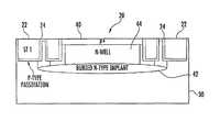
- FIG. 1shows a cross-sectional view of a circular STI-bounded SPAD (not to scale) in accordance with the present invention.
- the STI-interfacehas been passivated using multiple p-type implants, thus reducing the probability of minority carriers entering the multiplication region of the detector and triggering dark counts.
- FIG. 2is a plan view of the SPAD of FIG. 1 and the integrated test electronics implemented in 130 nm CMOS technology.
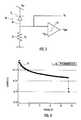
- FIG. 3is a schematic diagram of the SPAD of FIG. 1 and the integrated testing electronics.
- the passive quenching circuitis configured as a ballast resistor, and recharge is achieved passively through this circuit. Threshold detection and impedance conversion is implemented via the comparator.
- FIG. 6is a plot showing the dark count rate at room temperature as a function of the excess bias voltage in accordance with the present invention.
- FIG. 9is a graph showing the time response of the SPAD of FIG. 1 when illuminated by a picosecond light source at 637 nm wavelength and 1 V of excess bias voltage.
- FIG. 10shows an autocorrelation probability of the SPAD of FIG. 1 . No after-pulsing contribution could be measured.
- SPADs 20 for deep-submicron technologiesusually have an octagonal shape as disclosed in Finkelstein et al., “STI-Bounded Single-Photon Avalanche Diode in a Deep-Submicrometer CMOS Technology,” IEEE Electron Device Letters, vol. 27 (11), pp. 887-889, 2006; and Niclass et al., “A Single Photon Avalanche Diode Implementation in 130-nm CMOS Technology,” IEEE Journal of Selected Topics in Quantum Electronics, vol. 13, pp. 863-869, 2007. At the edges of the octagonal structures the electric field is significantly higher than in the rest of the multiplication region, thus creating regions of high noise contribution.
- the SPAD 20can be integrated along with an on-chip ballast resistance 52 and a comparator 54 , as best illustrated in FIG. 3 .
- the ballast resistance 52is used to perform passive quenching and recharge of the diode 20 when operating in the Geiger mode.
- the avalanche current flowing through the ballast resistor 52decreases the voltage across the diode 20 .
- the avalanche currentis no longer sustained and dies out.
- the SPAD 20is then passively recharged by a small current flowing through the ballast resistor 52 .
- the comparator 54with a proper threshold voltage V th , is used to convert the Geiger pulses into digital signals.
- FIG. 4shows a plot 60 in which the dark current is 5 ⁇ 10 ⁇ 11 A at the breakdown voltage of ⁇ 9.4 V.
- the guard ring structure 22 and the implementation of a round or circular SPAD 20allows for a significant reduction of the DCR from approximately 1 MHz as in Finkelstein et al., “STI-Bounded Single-Photon Avalanche Diode in a Deep-Submicrometer CMOS Technology,” IEEE Electron Device Letters, vol. 27 (11), pp. 887-889, 2006, to about 90 kHz at room temperature and at 1 volt of excess bias, while increasing the active area of the SPAD 20 .
- the DCRis similar to the device as in Niclass et al., “A Single Photon Avalanche Diode Implementation in 130-nm CMOS Technology,” IEEE Journal of Selected Topics in Quantum Electronics, vol. 13, pp. 863-869, 2007, the STI-based guard ring structure 22 allows for a significant improvement in the fill-factor shown as in the above-referenced Finkelstein et al. article.
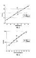
- FIG. 5provides plots 62 , 64 showing the temperature dependence of the DCR. The slopes indicate that due to the high doping levels, tunneling-induced dark counts are the dominating noise source over trap-assisted thermal generation.
- FIG. 6provides plots 66 , 68 showing the dark count rate at room temperature as a function of the excess bias voltage.
- the photoemission 70 shown in FIGS. 7 a and 7 bindicates that the electric field is distributed homogeneously or evenly across the sensitive region of the SPAD 20 . Furthermore, the absence of significant emission peaks at the border of the active region shows that the guard ring 22 is effective in lowering the electric field at the borders of the detector 20 . The region with low emission intensity going to the center 72 of the detector 20 was shielded by a metal line connecting the center of the p+ implant.
- the time response of the detector 20Another important measure for time-correlated applications is the time response of the detector 20 .
- the SPAD 20was illuminated by a picosecond laser diode source with a 637 nm wavelength (Advanced Laser Diode Systems GmBH, Berlin, Germany).
- the timing jitter at full-width-half-maximumwas measured to be 125 ps.
- the absorption of photons underneath the active region of the SPAD 20creates a tail 92 in the time response as the generated free carriers may diffuse back into the multiplication region.
- the use of a CMOS processallows the integration of the quenching resistance 52 and the read-out electronics 54 on-chip at the immediate surroundings of the detector 20 , thus limiting the parasitic capacitances.
- the correlation between subsequent breakdown eventswas measured.
- FIG. 10shows the autocorrelation curve 96 obtained. Note that after each breakdown event the SPAD 20 needed to recharge, and is thus inactive for a certain amount time. This period of time is known as the dead time. For the illustrated structure the dead time is approximately 18 ns. Therefore, in approximately the first 18 ns after a breakdown event, the autocorrelation is zero. When the SPAD 20 is fully recharged the autocorrelation is stable around one, this proving that no after-pulsing is present.
- the illustrated SPAD 20combines the advantages of deep-submicron processes, such as the possibility of integrating complex electronics and the improved fill-factor due to the STI-based guard ring 22 . This is while improving the noise performance of more than an order of magnitude when compared to comparable STI-bounded SPADs.
- the first integration of the illustrated SPADs 20 along with quenching 52 and read-out electronics 54 in 130 nm CMOS technologyshowed that no after-pulsing is present even with a dead time as short as 18 ns.
- optical measurements of the photoemission during avalanche breakdownproved the effectiveness of the guard ring structure 22 and the planarity or consistency of the multiplication region.
- Another aspectis directed to a method for reducing the dark count rate (DCR) by a photon avalanche detector 20 as described above.
- the methodcomprises forming a guard ring 22 in the semiconductor substrate 30 that at least partially surrounds the photon avalanche detector, and forming a passivation layer 24 of the first conductivity type in contact with the guard ring 22 to reduce the dark count rate by the photon avalanche detector 20 .
- the illustrated structurecombines shallow trench isolation (STI) and a passivation implant, thus creating an effective guard ring 22 against premature edge breakdown.
- STIshallow trench isolation
- a passivation implantthus creating an effective guard ring 22 against premature edge breakdown.
- high levels of miniaturizationmay be reached without detriment to noise, sensitivity and timing resolution.
- optical measurementsshow the effectiveness of the guard ring 22 and the high degree of electric field planarity or consistency across the sensitive region of the detector 20 .
- the SPAD 20is well suited for applications such as 3-D imaging, fluorescence lifetime imaging, and biophotonics.
Landscapes
- Light Receiving Elements (AREA)
Abstract
Description
| TABLE 1 | |||
| Performance | |||
| Min. | Typ. | Max. | Unit | |||
| PDP@Ve= 1 V | 18 | % | ||||
| PDP@Ve= 2 | 30 | % | ||||
| DCR@Ve= 1 | 90 | kHz | ||||
| Active Area | 58 | μm2 | ||||
| FWHM Time jitter | 125 | ps | ||||
| @Ve= 1 V | ||||||
| After-Pulsing | <0.01 | % | ||||
| Probability | ||||||
| Dead Time | 18 | ns | ||||
| Breakdown Voltage | 9.4 | V | ||||
Claims (15)
Priority Applications (1)
| Application Number | Priority Date | Filing Date | Title |
|---|---|---|---|
| US12/327,240US7898001B2 (en) | 2008-12-03 | 2008-12-03 | Single photon detector and associated methods for making the same |
Applications Claiming Priority (1)
| Application Number | Priority Date | Filing Date | Title |
|---|---|---|---|
| US12/327,240US7898001B2 (en) | 2008-12-03 | 2008-12-03 | Single photon detector and associated methods for making the same |
Publications (2)
| Publication Number | Publication Date |
|---|---|
| US20100133636A1 US20100133636A1 (en) | 2010-06-03 |
| US7898001B2true US7898001B2 (en) | 2011-03-01 |
Family
ID=42221995
Family Applications (1)
| Application Number | Title | Priority Date | Filing Date |
|---|---|---|---|
| US12/327,240ActiveUS7898001B2 (en) | 2008-12-03 | 2008-12-03 | Single photon detector and associated methods for making the same |
Country Status (1)
| Country | Link |
|---|---|
| US (1) | US7898001B2 (en) |
Cited By (5)
| Publication number | Priority date | Publication date | Assignee | Title |
|---|---|---|---|---|
| CN108231946A (en)* | 2017-12-21 | 2018-06-29 | 上海集成电路研发中心有限公司 | A kind of single photon avalanche diode detector structure and its manufacturing method |
| CN109713062A (en)* | 2018-12-24 | 2019-05-03 | 华中科技大学 | A kind of silicon avalanche optoelectronic detection chip and preparation method thereof |
| CN109904273A (en)* | 2019-01-08 | 2019-06-18 | 重庆邮电大学 | An Equivalent Circuit of a CMOS SPAD Photoelectric Device |
| US11189742B2 (en)* | 2018-04-11 | 2021-11-30 | Canon Kabushiki Kaisha | Photo-detection device, photo-detection system, and mobile apparatus |
| US11982566B2 (en) | 2019-03-29 | 2024-05-14 | Ecole Polytechnique Federale De Lausanne (Epfl) | System, device, and method for quantum correlation measurement with single photon avalanche diode arrays |
Families Citing this family (21)
| Publication number | Priority date | Publication date | Assignee | Title |
|---|---|---|---|---|
| GB201014843D0 (en) | 2010-09-08 | 2010-10-20 | Univ Edinburgh | Single photon avalanche diode for CMOS circuits |
| GB2485994A (en) | 2010-11-30 | 2012-06-06 | St Microelectronics Res & Dev | Navigation device using a Single Photon Avalanche Diode (SPAD) detector |
| GB2486165A (en) | 2010-11-30 | 2012-06-13 | St Microelectronics Res & Dev | Oven using a Single Photon Avalanche Diode (SPAD) array |
| GB2485993A (en)* | 2010-11-30 | 2012-06-06 | St Microelectronics Res & Dev | Sports equipment comprising proximity detector using single photon avalanche diode (SPAD) for measuring the speed of an object struck by the sports equipment |
| GB2494663A (en) | 2011-09-14 | 2013-03-20 | St Microelectronics Res & Dev | A system and corresponding method for monitoring vibration isolators |
| WO2013066959A1 (en)* | 2011-10-31 | 2013-05-10 | The Trustees Of Columbia University In The City Of New York | Systems and methods for imaging using single photon avalanche diodes |
| JP6090060B2 (en) | 2013-08-23 | 2017-03-08 | 株式会社豊田中央研究所 | Single photon avalanche diode |
| CN103779437A (en)* | 2014-02-17 | 2014-05-07 | 苏州超锐微电子有限公司 | Single-photon-level resolution ratio sensor unit structure based on standard CMOS technology |
| US9450007B1 (en)* | 2015-05-28 | 2016-09-20 | Stmicroelectronics S.R.L. | Integrated circuit with reflective material in trenches and related methods |
| US10971533B2 (en)* | 2018-01-29 | 2021-04-06 | Stmicroelectronics (Crolles 2) Sas | Vertical transfer gate with charge transfer and charge storage capabilities |
| JP7169071B2 (en)* | 2018-02-06 | 2022-11-10 | ソニーセミコンダクタソリューションズ株式会社 | Pixel structure, image pickup device, image pickup device, and electronic equipment |
| FR3098075A1 (en) | 2019-06-28 | 2021-01-01 | Stmicroelectronics (Crolles 2) Sas | Pixel and its ordering process |
| CN112909033A (en) | 2019-12-04 | 2021-06-04 | 半导体元件工业有限责任公司 | Semiconductor device with a plurality of transistors |
| US11764314B2 (en)* | 2019-12-04 | 2023-09-19 | Semiconductor Components Industries, Llc | Scattering structures for single-photon avalanche diodes |
| JP2021150359A (en)* | 2020-03-17 | 2021-09-27 | 株式会社東芝 | Photo detector, photo detection system, lidar device, and mobile body |
| FR3117672B1 (en)* | 2020-12-10 | 2023-12-08 | St Microelectronics Crolles 2 Sas | Integrated circuit comprising an avalanche diode triggered by individual photon and corresponding manufacturing method |
| CN114038865A (en)* | 2021-02-26 | 2022-02-11 | 神盾股份有限公司 | Single photon avalanche diode and single photon avalanche diode array |
| IT202100009434A1 (en)* | 2021-04-14 | 2022-10-14 | Fond Bruno Kessler | A RADIATION SENSOR |
| WO2022219515A1 (en)* | 2021-04-14 | 2022-10-20 | Fondazione Bruno Kessler | A diode radiation sensor |
| CN114420783A (en)* | 2022-02-10 | 2022-04-29 | 中国科学院上海技术物理研究所 | Mesa type avalanche single photon detector based on double avalanche mechanism |
| CN116072755B (en)* | 2023-03-09 | 2023-07-07 | 潍坊先进光电芯片研究院 | A silicon-based linear avalanche photodetector, preparation method and application |
Citations (6)
| Publication number | Priority date | Publication date | Assignee | Title |
|---|---|---|---|---|
| US20010017786A1 (en)* | 1999-08-17 | 2001-08-30 | Lucent Technologies Inc. | Integrated optoelectronic device with an avalanche photodetector and method of making the same using commercial CMOS processes |
| US20040056176A1 (en)* | 2002-09-20 | 2004-03-25 | Fuji Photo Film Co., Ltd. | Non-volatile solid state image pickup device and its drive |
| US20060163627A1 (en)* | 2004-07-08 | 2006-07-27 | Micron Technology, Inc. | Deuterated structures for image sensors and methods for forming the same |
| US20060192086A1 (en)* | 2005-02-14 | 2006-08-31 | Ecole Polytechnique Federale De Lausanne Epfl | Integrated imager circuit comprising a monolithic array of single photon avalanche diodes |
| US20090065704A1 (en)* | 2006-04-25 | 2009-03-12 | Koninklijke Philips Electronics N. V. | Implementation of avalanche photo diodes in (bi) cmos processes |
| US20100245809A1 (en)* | 2007-03-15 | 2010-09-30 | Johns Hopkins University | Deep submicron and nano cmos single photon photodetector pixel with event based circuits for readout data-rate reduction communication system |
- 2008
- 2008-12-03USUS12/327,240patent/US7898001B2/enactiveActive
Patent Citations (6)
| Publication number | Priority date | Publication date | Assignee | Title |
|---|---|---|---|---|
| US20010017786A1 (en)* | 1999-08-17 | 2001-08-30 | Lucent Technologies Inc. | Integrated optoelectronic device with an avalanche photodetector and method of making the same using commercial CMOS processes |
| US20040056176A1 (en)* | 2002-09-20 | 2004-03-25 | Fuji Photo Film Co., Ltd. | Non-volatile solid state image pickup device and its drive |
| US20060163627A1 (en)* | 2004-07-08 | 2006-07-27 | Micron Technology, Inc. | Deuterated structures for image sensors and methods for forming the same |
| US20060192086A1 (en)* | 2005-02-14 | 2006-08-31 | Ecole Polytechnique Federale De Lausanne Epfl | Integrated imager circuit comprising a monolithic array of single photon avalanche diodes |
| US20090065704A1 (en)* | 2006-04-25 | 2009-03-12 | Koninklijke Philips Electronics N. V. | Implementation of avalanche photo diodes in (bi) cmos processes |
| US20100245809A1 (en)* | 2007-03-15 | 2010-09-30 | Johns Hopkins University | Deep submicron and nano cmos single photon photodetector pixel with event based circuits for readout data-rate reduction communication system |
Non-Patent Citations (11)
| Title |
|---|
| Cohen, M et al, Fully Optimized Cu Based Process with Dedicated Cavity Etch for 1.75mum and 1.45mum Pixel Pitch CMOS Image Sensors:. |
| Cohen, M et al, Fully Optimized Cu Based Process with Dedicated Cavity Etch for 1.75μm and 1.45μm Pixel Pitch CMOS Image Sensors:. |
| Cova, Sergio et al, A Semiconductor Detector for Measuring Ultra weak Flourescence Decays with 70 ps. FWHM Resolution: IEEE Journal of Quatum Electronics, vol. QE-19, No. 4, Apr. 1983; pp. 630-634. |
| Faramarzpour, Naser et al. Fully Integrated Single Photon Avalanche Diode Detector in Standard CMOS 0.18- mum Technology: IEEE Transactions on Electron Devices, vol. 55, No. 3, Mar. 2008; pp. 760-767. |
| Faramarzpour, Naser et al. Fully Integrated Single Photon Avalanche Diode Detector in Standard CMOS 0.18- μm Technology: IEEE Transactions on Electron Devices, vol. 55, No. 3, Mar. 2008; pp. 760-767. |
| Finkelstein, Hod et al STI-Bounded Single-Photon Avalanche Diode in a Deep-Submicrometer CMOS Technology: IEEE Electron Device Letters, vol. 27, No. 11, Nov. 2006; pp. 887-889. |
| Gersbach, Marek et al, A Single Photon Detector implemented in a 130nm CMOS imaging Process: ESSDERC Conference, Edinburgh, Sep. 2008. |
| Niclass, Christiana et al, Toward a 3-D Camera Based on Single Photon Avalanche Diodes: IEEE Journal of Selected Topics in Quatum Electronics, vol. 10, No. 4, Jul./Aug. 2004; pp. 796-802. |
| Niclass, Cristiano et al A Single Photon Avalanche Diode Implemented in 130-nm CMOS Technology: IEEE Journal of Selected Topics in Quantum Electronics, vol. 13. No. 4, Jul./Aug. 2007; pp. 863-869. |
| Niclass, Cristiano et al, a 130nm Single Photon Avalanche Diode, IEEE Journal of Selected Topics in Quantum Electronics, vol. 13, Issue 4, Jul.-Aug. 2007, pp. 863-869. |
| Rochas, A. et al, Single Photon Detector Fabricated in a Complementary Metal-Oxide-Semiconductor High-voltage Technology: Review of Scientific Instruments, vol. 74, No. 7, Jul. 2003, pp. 3263-3270. |
Cited By (6)
| Publication number | Priority date | Publication date | Assignee | Title |
|---|---|---|---|---|
| CN108231946A (en)* | 2017-12-21 | 2018-06-29 | 上海集成电路研发中心有限公司 | A kind of single photon avalanche diode detector structure and its manufacturing method |
| CN108231946B (en)* | 2017-12-21 | 2020-01-10 | 上海集成电路研发中心有限公司 | Single photon avalanche diode detector structure and manufacturing method thereof |
| US11189742B2 (en)* | 2018-04-11 | 2021-11-30 | Canon Kabushiki Kaisha | Photo-detection device, photo-detection system, and mobile apparatus |
| CN109713062A (en)* | 2018-12-24 | 2019-05-03 | 华中科技大学 | A kind of silicon avalanche optoelectronic detection chip and preparation method thereof |
| CN109904273A (en)* | 2019-01-08 | 2019-06-18 | 重庆邮电大学 | An Equivalent Circuit of a CMOS SPAD Photoelectric Device |
| US11982566B2 (en) | 2019-03-29 | 2024-05-14 | Ecole Polytechnique Federale De Lausanne (Epfl) | System, device, and method for quantum correlation measurement with single photon avalanche diode arrays |
Also Published As
| Publication number | Publication date |
|---|---|
| US20100133636A1 (en) | 2010-06-03 |
Similar Documents
| Publication | Publication Date | Title |
|---|---|---|
| US7898001B2 (en) | Single photon detector and associated methods for making the same | |
| Gersbach et al. | A low-noise single-photon detector implemented in a 130 nm CMOS imaging process | |
| Sanzaro et al. | Single-photon avalanche diodes in a 0.16 μm BCD technology with sharp timing response and red-enhanced sensitivity | |
| US11837670B2 (en) | Semiconductor devices with single-photon avalanche diodes, light scattering structures, and multiple deep trench isolation structures | |
| US10217889B2 (en) | Clamped avalanche photodiode | |
| Bronzi et al. | SPAD figures of merit for photon-counting, photon-timing, and imaging applications: a review | |
| Veerappan et al. | A low dark count pin diode based SPAD in CMOS technology | |
| US8779543B2 (en) | Device having an avalanche photo diode and a method for sensing photons | |
| Leitner et al. | Measurements and simulations of low dark count rate single photon avalanche diode device in a low voltage 180-nm CMOS image sensor technology | |
| Gersbach et al. | A single photon detector implemented in a 130nm CMOS imaging process | |
| GB2557303A (en) | Photociode device and method of manufacture | |
| US12310139B2 (en) | Semiconductor devices with single-photon avalanche diodes and isolation structures | |
| US20220271177A1 (en) | Sensor and method of forming the same | |
| Gulinatti et al. | Improving the performance of silicon single-photon avalanche diodes | |
| US12027633B2 (en) | Scattering structures for single-photon avalanche diodes | |
| Van Sieleghem et al. | A backside-illuminated charge-focusing silicon SPAD with enhanced near-infrared sensitivity | |
| Liu et al. | A wide spectral response single photon avalanche diode for backside-illumination in 55-nm CMOS process | |
| Moreno-García et al. | Low-noise single photon avalanche diodes in a 110nm CIS technology | |
| US8212327B2 (en) | High fill-factor laser-treated semiconductor device on bulk material with single side contact scheme | |
| Liang et al. | Silicon Photomultipliers With Area Up to 9 mm 2 in a 0.35-$\mu $ m CMOS Process | |
| Wu et al. | Design and characterization of n/p-well CMOS SPAD with low dark count rate and high photon detection efficiency | |
| Liu et al. | Junction-Optimized SPAD With 50.6% Peak PDP and 0.64 cps/μm 2 DCR at 2 V Excess Bias Voltage in 130 nm CMOS | |
| Park et al. | A back-illuminated SPAD fabricated with 40 nm CMOS image sensor technology achieving near 40% PDP at 940 nm | |
| D’Ascenzo et al. | Design and Characterization of a Silicon Photomultiplier in 0.35-${\mu}\text {m} $ CMOS | |
| Wu et al. | Designing a sub-20V breakdown voltage SPAD with standard CMOS technology and n/p-well structure |
Legal Events
| Date | Code | Title | Description |
|---|---|---|---|
| AS | Assignment | Owner name:STMICROELECTRONICS (RESEARCH & DEVELOPMENT) LIMITE Free format text:ASSIGNMENT OF ASSIGNORS INTEREST;ASSIGNORS:RICHARDSON, JUSTIN;GRANT, LINDSAY;GERBACH, MAREK;AND OTHERS;SIGNING DATES FROM 20090106 TO 20090108;REEL/FRAME:022211/0244 Owner name:THE UNIVERSITY COURT OF THE UNIVERSITY OF EDINBURG Free format text:ASSIGNMENT OF ASSIGNORS INTEREST;ASSIGNORS:RICHARDSON, JUSTIN;GRANT, LINDSAY;GERBACH, MAREK;AND OTHERS;SIGNING DATES FROM 20090106 TO 20090108;REEL/FRAME:022211/0244 Owner name:ECOLE POLYTECHNIQUE FEDERALE DE LAUSANNE,SWITZERLA Free format text:ASSIGNMENT OF ASSIGNORS INTEREST;ASSIGNORS:RICHARDSON, JUSTIN;GRANT, LINDSAY;GERBACH, MAREK;AND OTHERS;SIGNING DATES FROM 20090106 TO 20090108;REEL/FRAME:022211/0244 Owner name:ECOLE POLYTECHNIQUE FEDERALE DE LAUSANNE, SWITZERL Free format text:ASSIGNMENT OF ASSIGNORS INTEREST;ASSIGNORS:RICHARDSON, JUSTIN;GRANT, LINDSAY;GERBACH, MAREK;AND OTHERS;SIGNING DATES FROM 20090106 TO 20090108;REEL/FRAME:022211/0244 | |
| AS | Assignment | Owner name:STMICROELECTRONICS (RESEARCH & DEVELOPMENT) LIMITE Free format text:CORRECTIVE ASSIGNMENT TO CORRECT THE THIRD INVENTOR'S NAME PREVIOUSLY RECORDED ON REEL 022211 FRAME 0244. ASSIGNOR(S) HEREBY CONFIRMS THE ASSIGNMENT OF ASSIGNOR'S INTEREST;ASSIGNORS:RICHARDSON, JUSTIN;GRANT, LINDSAY;GERSBACH, MAREK;AND OTHERS;SIGNING DATES FROM 20090106 TO 20090108;REEL/FRAME:022404/0228 Owner name:THE UNIVERSITY COURT OF THE UNIVERSITY OF EDINBURG Free format text:CORRECTIVE ASSIGNMENT TO CORRECT THE THIRD INVENTOR'S NAME PREVIOUSLY RECORDED ON REEL 022211 FRAME 0244. ASSIGNOR(S) HEREBY CONFIRMS THE ASSIGNMENT OF ASSIGNOR'S INTEREST;ASSIGNORS:RICHARDSON, JUSTIN;GRANT, LINDSAY;GERSBACH, MAREK;AND OTHERS;SIGNING DATES FROM 20090106 TO 20090108;REEL/FRAME:022404/0228 Owner name:ECOLE POLYTECHNIQUE FEDERALE DE LAUSANNE,SWITZERLA Free format text:CORRECTIVE ASSIGNMENT TO CORRECT THE THIRD INVENTOR'S NAME PREVIOUSLY RECORDED ON REEL 022211 FRAME 0244. ASSIGNOR(S) HEREBY CONFIRMS THE ASSIGNMENT OF ASSIGNOR'S INTEREST;ASSIGNORS:RICHARDSON, JUSTIN;GRANT, LINDSAY;GERSBACH, MAREK;AND OTHERS;SIGNING DATES FROM 20090106 TO 20090108;REEL/FRAME:022404/0228 Owner name:ECOLE POLYTECHNIQUE FEDERALE DE LAUSANNE, SWITZERL Free format text:CORRECTIVE ASSIGNMENT TO CORRECT THE THIRD INVENTOR'S NAME PREVIOUSLY RECORDED ON REEL 022211 FRAME 0244. ASSIGNOR(S) HEREBY CONFIRMS THE ASSIGNMENT OF ASSIGNOR'S INTEREST;ASSIGNORS:RICHARDSON, JUSTIN;GRANT, LINDSAY;GERSBACH, MAREK;AND OTHERS;SIGNING DATES FROM 20090106 TO 20090108;REEL/FRAME:022404/0228 | |
| STCF | Information on status: patent grant | Free format text:PATENTED CASE | |
| CC | Certificate of correction | ||
| FPAY | Fee payment | Year of fee payment:4 | |
| MAFP | Maintenance fee payment | Free format text:PAYMENT OF MAINTENANCE FEE, 8TH YEAR, LARGE ENTITY (ORIGINAL EVENT CODE: M1552); ENTITY STATUS OF PATENT OWNER: LARGE ENTITY Year of fee payment:8 | |
| MAFP | Maintenance fee payment | Free format text:PAYMENT OF MAINTENANCE FEE, 12TH YEAR, LARGE ENTITY (ORIGINAL EVENT CODE: M1553); ENTITY STATUS OF PATENT OWNER: LARGE ENTITY Year of fee payment:12 |