US7897980B2 - Expandable LED array interconnect - Google Patents
Expandable LED array interconnectDownload PDFInfo
- Publication number
- US7897980B2 US7897980B2US11/595,720US59572006AUS7897980B2US 7897980 B2US7897980 B2US 7897980B2US 59572006 AUS59572006 AUS 59572006AUS 7897980 B2US7897980 B2US 7897980B2
- Authority
- US
- United States
- Prior art keywords
- substrate
- led array
- top surface
- edges
- light emitting
- Prior art date
- Legal status (The legal status is an assumption and is not a legal conclusion. Google has not performed a legal analysis and makes no representation as to the accuracy of the status listed.)
- Active, expires
Links
Images

Classifications
- F—MECHANICAL ENGINEERING; LIGHTING; HEATING; WEAPONS; BLASTING
- F21—LIGHTING
- F21S—NON-PORTABLE LIGHTING DEVICES; SYSTEMS THEREOF; VEHICLE LIGHTING DEVICES SPECIALLY ADAPTED FOR VEHICLE EXTERIORS
- F21S2/00—Systems of lighting devices, not provided for in main groups F21S4/00 - F21S10/00 or F21S19/00, e.g. of modular construction
- F21S2/005—Systems of lighting devices, not provided for in main groups F21S4/00 - F21S10/00 or F21S19/00, e.g. of modular construction of modular construction
- F—MECHANICAL ENGINEERING; LIGHTING; HEATING; WEAPONS; BLASTING
- F21—LIGHTING
- F21K—NON-ELECTRIC LIGHT SOURCES USING LUMINESCENCE; LIGHT SOURCES USING ELECTROCHEMILUMINESCENCE; LIGHT SOURCES USING CHARGES OF COMBUSTIBLE MATERIAL; LIGHT SOURCES USING SEMICONDUCTOR DEVICES AS LIGHT-GENERATING ELEMENTS; LIGHT SOURCES NOT OTHERWISE PROVIDED FOR
- F21K9/00—Light sources using semiconductor devices as light-generating elements, e.g. using light-emitting diodes [LED] or lasers
- F—MECHANICAL ENGINEERING; LIGHTING; HEATING; WEAPONS; BLASTING
- F21—LIGHTING
- F21Y—INDEXING SCHEME ASSOCIATED WITH SUBCLASSES F21K, F21L, F21S and F21V, RELATING TO THE FORM OR THE KIND OF THE LIGHT SOURCES OR OF THE COLOUR OF THE LIGHT EMITTED
- F21Y2105/00—Planar light sources
- F21Y2105/10—Planar light sources comprising a two-dimensional array of point-like light-generating elements
- F—MECHANICAL ENGINEERING; LIGHTING; HEATING; WEAPONS; BLASTING
- F21—LIGHTING
- F21Y—INDEXING SCHEME ASSOCIATED WITH SUBCLASSES F21K, F21L, F21S and F21V, RELATING TO THE FORM OR THE KIND OF THE LIGHT SOURCES OR OF THE COLOUR OF THE LIGHT EMITTED
- F21Y2107/00—Light sources with three-dimensionally disposed light-generating elements
- F21Y2107/40—Light sources with three-dimensionally disposed light-generating elements on the sides of polyhedrons, e.g. cubes or pyramids
- F—MECHANICAL ENGINEERING; LIGHTING; HEATING; WEAPONS; BLASTING
- F21—LIGHTING
- F21Y—INDEXING SCHEME ASSOCIATED WITH SUBCLASSES F21K, F21L, F21S and F21V, RELATING TO THE FORM OR THE KIND OF THE LIGHT SOURCES OR OF THE COLOUR OF THE LIGHT EMITTED
- F21Y2115/00—Light-generating elements of semiconductor light sources
- F21Y2115/10—Light-emitting diodes [LED]
- F—MECHANICAL ENGINEERING; LIGHTING; HEATING; WEAPONS; BLASTING
- F21—LIGHTING
- F21Y—INDEXING SCHEME ASSOCIATED WITH SUBCLASSES F21K, F21L, F21S and F21V, RELATING TO THE FORM OR THE KIND OF THE LIGHT SOURCES OR OF THE COLOUR OF THE LIGHT EMITTED
- F21Y2115/00—Light-generating elements of semiconductor light sources
- F21Y2115/30—Semiconductor lasers
- H—ELECTRICITY
- H01—ELECTRIC ELEMENTS
- H01L—SEMICONDUCTOR DEVICES NOT COVERED BY CLASS H10
- H01L25/00—Assemblies consisting of a plurality of semiconductor or other solid state devices
- H01L25/03—Assemblies consisting of a plurality of semiconductor or other solid state devices all the devices being of a type provided for in a single subclass of subclasses H10B, H10D, H10F, H10H, H10K or H10N, e.g. assemblies of rectifier diodes
- H01L25/04—Assemblies consisting of a plurality of semiconductor or other solid state devices all the devices being of a type provided for in a single subclass of subclasses H10B, H10D, H10F, H10H, H10K or H10N, e.g. assemblies of rectifier diodes the devices not having separate containers
- H01L25/075—Assemblies consisting of a plurality of semiconductor or other solid state devices all the devices being of a type provided for in a single subclass of subclasses H10B, H10D, H10F, H10H, H10K or H10N, e.g. assemblies of rectifier diodes the devices not having separate containers the devices being of a type provided for in group H10H20/00
- H01L25/0753—Assemblies consisting of a plurality of semiconductor or other solid state devices all the devices being of a type provided for in a single subclass of subclasses H10B, H10D, H10F, H10H, H10K or H10N, e.g. assemblies of rectifier diodes the devices not having separate containers the devices being of a type provided for in group H10H20/00 the devices being arranged next to each other
- H—ELECTRICITY
- H01—ELECTRIC ELEMENTS
- H01L—SEMICONDUCTOR DEVICES NOT COVERED BY CLASS H10
- H01L2924/00—Indexing scheme for arrangements or methods for connecting or disconnecting semiconductor or solid-state bodies as covered by H01L24/00
- H01L2924/0001—Technical content checked by a classifier
- H01L2924/0002—Not covered by any one of groups H01L24/00, H01L24/00 and H01L2224/00
Definitions
- the inventionrelates to lighting systems, and more particularly to interconnected light emitting diode (LED) arrays.
- LEDlight emitting diode
- LEDsare semiconductor photon sources that can serve as highly efficient electronic-to-photonic transducers. They are typically forward-biased p-n junctions fabricated from a semiconductor material that emit light via injection electroluminescence. Their small size, high efficiency, high reliability, and compatibility with electronic systems make them very useful for a multitude of applications. Recent advancements have yielded high-power LEDs in a range of colors. This new generation of LEDs is useful in applications requiring a higher intensity light output such as high-power flash lights, airplane lighting systems, fiber-optic communication systems, and optical data storage systems.
- High-flux lighting solutionsare required by various modern applications such as street lighting, airport/airplane lighting systems, pool lighting systems, and many others.
- multiple LEDsare often arranged in various configurations or arrays. These arrays may take nearly any shape and usually include several individual LEDs.
- LED arraysmay be grouped together on a surface. Providing the necessary electrical connections to power the LED arrays can be challenging. The layout of the individual LEDs on the array surface determines where the input and output connections must be located on the surface and how the LED arrays must be arranged so that they can be connected together.
- circuitry needed to connect the arrayscan become complex and expensive.
- the circuit topology required to power the arraysoften requires circuit elements that cannot be mounted on the surface of the arrays. This can result in circuit elements that obscure the light emitters and prevent the light from escaping to the outside environment, greatly decreasing the efficiency of the arrays.
- One embodiment of a light emitting devicecomprises a substrate shaped to have a top surface and a plurality of edges.
- An input terminalis disposed on the top surface to be accessible from a plurality of the edges of the substrate.
- An output terminalis disposed on the top surface to be accessible from a plurality of the edges of the substrate.
- At least one lighting elementis mounted to the top surface of the substrate and connected between the input terminal and the output terminal.
- an LED array elementcomprises a substrate shaped as a regular hexagon having six edges and a top surface.
- An input terminalis disposed on the top surface of the substrate to be accessible from three of the substrate edges.
- An output terminalis disposed on the top surface of the substrate to be accessible from three of the substrate edges opposite the input terminal.
- At least one LEDis mounted to the top surface of the substrate and connected between the input terminal and the output terminal.
- One embodiment of an expandable LED array according to the present inventioncomprises a plurality of LED array elements arranged in an expandable tiling on a surface, each of the LED array elements having at least one LED, and each of the LED array elements having an input terminal with multiple contact pads and an output terminal with multiple contact pads.
- a network of conductorsis connected to provide power to the plurality of LED array elements.
- FIG. 1is a top plan view of a light emitting device according to one embodiment of the present invention.
- FIG. 2is a side view of a light emitting device according to one embodiment of the present invention.
- FIG. 3is a top plan view of a plurality of light emitting devices arranged in an array according to one embodiment of the present invention.
- FIG. 4is a top plan view of a plurality of LED array elements arranged in a tiling on a flat surface according to one embodiment of the present invention.
- FIG. 5is a perspective view of a plurality of LED array elements arranged in a tiling on a three-dimensional surface according to one embodiment of the present invention.
- the present inventionrelates to light emitting devices, and in particular, light emitting devices that can be used as individual array elements that can be arranged in a pattern to increase luminescent output.
- the inventionalso relates to an expandable array of light emitting elements (e.g., LEDs).
- at least one light emitteris disposed on a substrate and connected between input and output terminals located on opposite sides of the substrate. Multiple emitters may be disposed on the substrate in a pattern. These emitters may be connected between the input and output terminals serially, in parallel, or in a combination thereof.
- the input and output terminalsare disposed on the top surface of the substrate along the edges such that they are accessible from a plurality of the edges.
- the devicesfunction as array elements in an expandable array. Grouping several array elements together increases the total light output.
- the array elementsare specifically shaped to fit efficiently with other array elements onto a surface.
- the array elementsmay be shaped as regular polygons (e.g., squares, hexagons or octagons) or any other shape that meets design needs.
- the accessibility of the terminals from multiple sides of the elementsprovides the designer with many options for a current path from the power source through each of the array elements.
- the array elementsmay be mounted to a two-dimensional surface or a three-dimensional surface.
- first, second, etc.may be used herein to describe various elements, components, regions, layers and/or sections, these elements, components, regions, layers and/or sections should not be limited by these terms. These terms are only used to distinguish one element, component, region, layer or section from another region, layer or section. Thus, a first element, component, region, layer or section discussed below could be termed a second element, component, region, layer or section without departing from the teachings of the present invention.
- Embodiments of the inventionare described herein with reference to various illustrations that are schematic illustrations of idealized embodiments of the invention. As such, variations from the shapes of the illustrations as a result, for example, of manufacturing techniques and/or tolerances are expected. Embodiments of the invention should not be construed as limited to the particular shapes of the regions illustrated herein but are to include deviations in shapes that result, for example, from manufacturing. Thus, the devices illustrated in the figures are schematic in nature and are not intended to limit the scope of the invention.
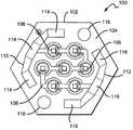
- FIG. 1shows one embodiment of a light emitting device 100 according to the present invention.
- Light emitting device 100can serve as an array element when linking several of the devices together to increase luminescent output.
- Substrate 102comprises top surface 104 and a bottom surface (not shown). Substrate 102 may be made from various materials, with the preferable material being a printed circuit board (PCB) material. Various electronic and optical components are disposed on top surface 104 , including but not limited to resistors, capacitors, transistors, conductors, lenses, or any other active or passive elements. These components should include at least one light emitting element 106 . Such light emitting components may include vertical cavity surface emitting lasers (VCSELs), light emitting diodes (LEDs), or other semiconductor devices.
- VCSELsvertical cavity surface emitting lasers
- LEDslight emitting diodes
- the light emitting elements 106are mounted to top surface 104 . Light emitting elements 106 are shown connected in series via trace 108 which is disposed on top surface 104 . The light emitting elements can also be connected in a parallel configuration or in a combination of series and parallel connections. Input terminal 110 is located near the edges of substrate 102 . Output terminal 112 is located near the opposite edges of substrate 102 across from input terminal 110 . FIG. 1 shows input and output terminals 110 , 112 shaped as segmented arcs. This shape allows terminals 110 , 112 to be accessible from multiple sides of substrate 102 . The terminals may be shaped in many other ways to accomplish the same degree of accessibility. Current from a power source (not shown) flows from input terminal 110 through light emitting elements 106 to output terminal 112 , illuminating the device 100 .
- Substrate 102can have many different shapes with a preferred shape being a regular hexagon. However, substrate 102 may also be shaped as a regular polygon such as a square, a pentagon, etc. Substrate 102 may also be shaped as an irregular polygon. Substrate 102 as shown in FIG. 1 is a regular hexagon having six edges of substantially equal length.
- input terminal 110is disposed along three adjacent edges. Input terminal 110 comprises three input contact pads 114 , each of which is located near to a corresponding one of the three input-side edges.
- Output terminal 112comprises three output contact pads 116 which are located near the three adjacent edges on the output-side, opposite the input terminal 110 .
- the input and output contact pads 114 , 116can be disposed on top surface 104 along the edges to provide easy access to the input and output terminals 110 , 112 .
- Contact pads 114 , 116may be made of any conductive material such as copper, gold or silver.
- Contact pads 114 , 116may be shaped by coating a portion of their respective terminals with a non-conductive material, thus defining the shape of each contact pad. This may be accomplished using a solder mask, for example. Shaping the contact pads provides a defined space for solder connections should those types of connections be used.
- light emitting elements 106may be mounted to top surface 104 .
- the light emitting elementscan be arranged in many different configurations on top surface 104 .
- the light emitting elementscan be connected in parallel, in series, or in a combination of both to achieve a desired light output.
- a preferred patterncomprises seven light emitting elements 106 arranged in a serial serpentine pattern as shown in FIG. 1 . Current flows from input terminal 110 through all of the light emitting elements 106 to output terminal 112 .
- Bore holes 118can be disposed near opposite vertices between the outer input and output contact pads 114 , 116 . Bore holes 118 are used to facilitate mounting the devices to a surface using screws or mounting pins. They can be sized to accommodate a variety of screws or mounting pins. Other mounting methods may also be used such as affixing the devices to a surface using thermally conductive epoxy or solder. The devices may be mounted to several different types of surfaces, such as metals or plastics. For example, because the devices can generate large amounts of heat during operation, it may be desirable to mount the devices to a thermally conductive surface capable of drawing excess heat away from the devices (i.e., a heat sink).
- FIG. 2is a side front view of a light emitting device 100 according to one embodiment of the present invention.
- Light emitting device 100has a top surface 104 and a bottom surface 202 .
- Lighting elements 106are mounted to top surface and electrically connected.
- FIG. 2illustrates one such design.
- Heat spreader 204has a high thermal conductivity over a broad range of temperatures and is disposed beneath top surface 104 .
- Heat spreader 204may be made from copper and aluminum, for example; although it could also be made from any high thermal conductivity material. In the design shown in FIG. 2 , heat spreader 204 forms the bottom surface 202 of the device.
- the embodiment of light emitting device 100 as illustrated in FIG. 2is oriented such that input terminal 110 (not visible in this view) is on the left-hand side of the figure as indicated by the positive sign (+) Likewise the output terminal 112 (not visible in this view) is on the right-hand as indicated by the negative sign ( ⁇ ). In this embodiment viewed from this orientation, an output contact pad 116 (not visible in this view) is disposed near the front edge.
- Bore holes 206are shown with hashed lines to indicate that they are set off a distance from the front edge of device 100 .
- the holes 206pass through top and bottom surfaces 104 , 202 , allowing device 100 to be easily mounted to other surfaces.
- devices 100can be mounted to a surface in several different ways including but not limited to methods using screws, epoxy adhesives and solders.
- FIG. 3is a top plan view of three light emitting devices 302 , 304 , 306 according to one embodiment of the present invention.
- Devices 302 , 304 , 306are connected in a serial arrangement.
- the arrowsindicate the direction of current flow through the devices.
- Currentflows into 302 at one of the edges marked with a positive (+).
- the currentthen flows through the light emitters (not shown), out of device 302 at one of the edges marked with a negative sign ( ⁇ ), and into one of the positive edges of device 304 .
- Device 306is, shown positioned adjacent to the middle negative edge of device 304 .
- device 306can also be disposed in either of two alternate positions 308 (shown with hashed lines). Because the positive and negative terminals are easily accessible from multiple sides of each device, there is a great deal of flexibility in designing the layout of the devices in an array and the path through which current will flow.
- the layout of FIG. 3is just one simple example of an array of devices and is meant to illustrate the additional freedom of design afforded by various embodiments of the invention.
- One of skill in the artwill recognize that the devices can be easily rotated, shifted and expanded to achieve a desired layout and current flow. An example of such an array is described below and illustrated in FIG. 4 .
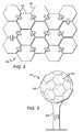
- FIG. 4is a top plan view of an array 400 of light emitting devices 100 according to one embodiment of the present invention.
- Devices 100function as array elements and are arranged in a tiling which can be expanded in all directions to accommodate luminescent output requirements.
- Devices 100are oriented such that edges of the respective devices that face each other are parallel. Spacing between the devices 100 can vary according to design specifications, for example, to accommodate different types of conductors.
- the devices 100are mounted on a flat surface.
- the design engineerhas a great deal of flexibility in arranging the array elements.
- the arraycan be expanded in any direction, allowing for various circuit connection schemes and increasing output efficiency.
- array elementshaving different shapes such as squares, pentagons, or octagons, for example. Combinations of such shapes may also be used to develop a specific array layout.
- FIG. 5is a perspective view of a three-dimensional (3-D) array 500 of light emitting devices 504 according to one embodiment of the present invention.
- Devices 504may be mounted to the surface of a 3-D structure 502 to achieve omnidirectional luminescence.
- This particular embodimentcomprises hexagonal and pentagonal array elements 504 that correspond to the substantially spherical 3-D structure 502 on which the devices 504 are mounted.
- the structure 502is mounted on a support 506 .
- Currentmay be delivered from a power source (not shown) either external to the structure 502 or from within the structure 502 or the support 506 .
- a power sourceexternal to the structure 502 .
- Currentflows through some or all of the array elements 504 and back out of the structure 502 as shown by the polarity arrows.
- Alternate embodimentsmay include structures having any 3-D shape. Array elements that are mounted to those structures may also come in any shape in order to efficiently cover part or all of the surface of the structure.
Landscapes
- Engineering & Computer Science (AREA)
- General Engineering & Computer Science (AREA)
- Physics & Mathematics (AREA)
- Microelectronics & Electronic Packaging (AREA)
- Optics & Photonics (AREA)
- Led Device Packages (AREA)
Abstract
Description
Claims (22)
Priority Applications (4)
| Application Number | Priority Date | Filing Date | Title |
|---|---|---|---|
| US11/595,720US7897980B2 (en) | 2006-11-09 | 2006-11-09 | Expandable LED array interconnect |
| JP2007228699AJP6093495B2 (en) | 2006-11-09 | 2007-09-04 | Light emitting device, LED array element, and light emitting device |
| DE102007042761.3ADE102007042761B4 (en) | 2006-11-09 | 2007-09-07 | Expandable LED array interconnection |
| US11/982,276US10295147B2 (en) | 2006-11-09 | 2007-10-31 | LED array and method for fabricating same |
Applications Claiming Priority (1)
| Application Number | Priority Date | Filing Date | Title |
|---|---|---|---|
| US11/595,720US7897980B2 (en) | 2006-11-09 | 2006-11-09 | Expandable LED array interconnect |
Related Child Applications (1)
| Application Number | Title | Priority Date | Filing Date |
|---|---|---|---|
| US11/982,276Continuation-In-PartUS10295147B2 (en) | 2006-11-09 | 2007-10-31 | LED array and method for fabricating same |
Publications (2)
| Publication Number | Publication Date |
|---|---|
| US20080111470A1 US20080111470A1 (en) | 2008-05-15 |
| US7897980B2true US7897980B2 (en) | 2011-03-01 |
Family
ID=39339055
Family Applications (1)
| Application Number | Title | Priority Date | Filing Date |
|---|---|---|---|
| US11/595,720Active2027-01-06US7897980B2 (en) | 2006-11-09 | 2006-11-09 | Expandable LED array interconnect |
Country Status (3)
| Country | Link |
|---|---|
| US (1) | US7897980B2 (en) |
| JP (1) | JP6093495B2 (en) |
| DE (1) | DE102007042761B4 (en) |
Cited By (29)
| Publication number | Priority date | Publication date | Assignee | Title |
|---|---|---|---|---|
| US20080133782A1 (en)* | 2006-12-01 | 2008-06-05 | Lg Electronics Inc. | Reception system and method of processing interface information |
| US20090050908A1 (en)* | 2005-01-10 | 2009-02-26 | Cree, Inc. | Solid state lighting component |
| US20100103660A1 (en)* | 2008-10-24 | 2010-04-29 | Cree Led Lighting Solutions, Inc. | Array layout for color mixing |
| US20100123380A1 (en)* | 2008-11-19 | 2010-05-20 | Sinology Enterprise Ltd. | Modular Structure of LED Light Source |
| US20100254129A1 (en)* | 2006-04-18 | 2010-10-07 | Cree, Inc. | Saturated yellow phosphor converted led and blue converted red led |
| US20110043137A1 (en)* | 2009-08-19 | 2011-02-24 | Cree Led Lighting Solutions, Inc. | White light color changing solid state lighting and methods |
| US20110148327A1 (en)* | 2009-12-21 | 2011-06-23 | Van De Ven Antony P | High cri adjustable color temperature lighting devices |
| US20110193061A1 (en)* | 2009-04-10 | 2011-08-11 | Everlight Yi-Guang Technology (Shanghai) Ltd | Light Emitting Diode Device Having Uniform Current Distribution and Method for Forming the Same |
| US20110222280A1 (en)* | 2010-06-01 | 2011-09-15 | Choong Youl Kim | Light emitting device package and lighting system |
| US20120044679A1 (en)* | 2010-08-17 | 2012-02-23 | Lextar Electronics Corporation | Point light source and light source module using the same |
| US8322906B2 (en) | 2011-08-08 | 2012-12-04 | XtraLight Manufacturing Partnership Ltd | Versatile lighting units |
| US20130009179A1 (en)* | 2011-07-06 | 2013-01-10 | Cree, Inc. | Compact optically efficient solid state light source with integrated thermal management |
| US20130194815A1 (en)* | 2012-01-30 | 2013-08-01 | Bridgelux, Inc. | Circuit Board for LED Applications |
| US20130215614A1 (en)* | 2011-05-13 | 2013-08-22 | Reliance Laboratories, Llc | Modular light emitting diode systems and devices |
| US20140056003A1 (en)* | 2012-08-20 | 2014-02-27 | John Frattalone | Modular video and lighting displays |
| USD700584S1 (en) | 2011-07-06 | 2014-03-04 | Cree, Inc. | LED component |
| US8698171B2 (en) | 2005-01-10 | 2014-04-15 | Cree, Inc. | Solid state lighting component |
| US20140270735A1 (en)* | 2013-03-12 | 2014-09-18 | Applied Materials, Inc. | High density solid state light source array |
| US8921873B2 (en) | 2012-09-25 | 2014-12-30 | Toyoda Gosei Co., Ltd. | Light-emitting device |
| US9097414B2 (en) | 2010-08-30 | 2015-08-04 | Osram Oled Gmbh | Light source device on a printed circuit board and light source arrangement comprising a plurality of light source devices |
| US20160123569A1 (en)* | 2013-06-07 | 2016-05-05 | Modulux Lighting, Inc. | Modular luminaire system |
| US20160240518A1 (en)* | 2015-02-13 | 2016-08-18 | Nichia Corporation | Light emitting device |
| US9644829B2 (en) | 2013-04-25 | 2017-05-09 | Xtralight Manufacturing, Ltd. | Systems and methods for providing a field repairable light fixture with a housing that dissipates heat |
| US9786811B2 (en) | 2011-02-04 | 2017-10-10 | Cree, Inc. | Tilted emission LED array |
| US20180156397A1 (en)* | 2015-07-31 | 2018-06-07 | Chi Wai Patrick Poon | Pcb electroplating and electrical connection box structure and modular luminaire |
| US10043960B2 (en)* | 2011-11-15 | 2018-08-07 | Cree, Inc. | Light emitting diode (LED) packages and related methods |
| US10295147B2 (en) | 2006-11-09 | 2019-05-21 | Cree, Inc. | LED array and method for fabricating same |
| US10317049B2 (en)* | 2015-11-16 | 2019-06-11 | Ushio Denki Kabushiki Kaisha | Light irradiation device |
| US11791442B2 (en) | 2007-10-31 | 2023-10-17 | Creeled, Inc. | Light emitting diode package and method for fabricating same |
Families Citing this family (14)
| Publication number | Priority date | Publication date | Assignee | Title |
|---|---|---|---|---|
| DE102007009229B4 (en)* | 2007-02-26 | 2015-01-08 | Zumtobel Lighting Gmbh | Light source for simulating a point light source, and light with such a light source |
| JP4642129B2 (en)* | 2008-11-06 | 2011-03-02 | ローム株式会社 | LED lamp |
| JP5161126B2 (en)* | 2009-01-29 | 2013-03-13 | 財団法人山形県産業技術振興機構 | Lighting device |
| JP2011066133A (en)* | 2009-09-16 | 2011-03-31 | Koito Mfg Co Ltd | Light-emitting module and vehicular lighting fixture |
| CN102577635B (en) | 2009-09-17 | 2015-03-25 | 皇家飞利浦电子股份有限公司 | Light-source module and light-emitting device |
| US20110134641A1 (en)* | 2009-12-07 | 2011-06-09 | Chen Hong-Yuan | Composite structure for polygonal light-emitting diode |
| TWM412319U (en) | 2010-11-01 | 2011-09-21 | Parlux Optoelectronics Corp | LED illumination device |
| IN2014CN04515A (en)* | 2011-12-05 | 2015-09-11 | Koninkl Philips Nv | |
| JPWO2013099074A1 (en)* | 2011-12-27 | 2016-05-26 | パナソニック株式会社 | Lamp and lighting apparatus using the same |
| EP2864696A4 (en) | 2012-06-26 | 2015-12-02 | Num Lighting Ltd | A modular light system |
| EP2725284A1 (en)* | 2012-10-23 | 2014-04-30 | Allnet GmbH | Interconnectable LED modules and method of interconnecting LED modules |
| USD825818S1 (en)* | 2017-12-20 | 2018-08-14 | Contemporary Visions, LLC | Light fixture |
| USD825817S1 (en)* | 2017-12-20 | 2018-08-14 | Contemporary Visions, LLC | Light fixture |
| USD825816S1 (en)* | 2017-12-20 | 2018-08-14 | Contemporary Visions, LLC | Light fixture |
Citations (26)
| Publication number | Priority date | Publication date | Assignee | Title |
|---|---|---|---|---|
| WO2000033390A1 (en) | 1998-11-30 | 2000-06-08 | General Electric Company | Light emitting device with phosphor composition |
| JP2002050799A (en) | 2000-08-04 | 2002-02-15 | Stanley Electric Co Ltd | LED lamp and manufacturing method thereof |
| JP2002076446A (en) | 2000-03-27 | 2002-03-15 | General Electric Co <Ge> | Single phosphor for producing white light with high visibility and CRI in UV light emitting LED devices |
| US6422716B2 (en) | 2000-03-16 | 2002-07-23 | Bjb Gmbh & Co. Kg | Modular led assembly |
| US6452217B1 (en)* | 2000-06-30 | 2002-09-17 | General Electric Company | High power LED lamp structure using phase change cooling enhancements for LED lighting products |
| JP2002531955A (en) | 1998-11-30 | 2002-09-24 | ゼネラル・エレクトリック・カンパニイ | Light emitting device using phosphor with high visibility |
| US20020153529A1 (en)* | 2001-04-24 | 2002-10-24 | Jin-Shown Shie | LED array with optical isolation structure and method of manufacturing the same |
| US20020171089A1 (en)* | 2001-03-06 | 2002-11-21 | Hiroyuki Okuyama | Display unit and semiconductor light emitting device |
| US20020171090A1 (en)* | 2001-05-15 | 2002-11-21 | Toyoharu Oohata | Display device and display unit using the same |
| US6498355B1 (en) | 2001-10-09 | 2002-12-24 | Lumileds Lighting, U.S., Llc | High flux LED array |
| US6501100B1 (en) | 2000-05-15 | 2002-12-31 | General Electric Company | White light emitting phosphor blend for LED devices |
| WO2003021668A1 (en) | 2001-08-31 | 2003-03-13 | Hitachi Chemical Co.,Ltd. | Wiring board, semiconductor device and method for producing them |
| JP2003318448A (en) | 2002-02-19 | 2003-11-07 | Nichia Chem Ind Ltd | Light emitting device and method for forming the same |
| US6653765B1 (en) | 2000-04-17 | 2003-11-25 | General Electric Company | Uniform angular light distribution from LEDs |
| US6803732B2 (en) | 2001-12-20 | 2004-10-12 | Osram Opto Semiconductors Gmbh | LED array and LED module with chains of LEDs connected in parallel |
| US6891200B2 (en)* | 2001-01-25 | 2005-05-10 | Matsushita Electric Industrial Co., Ltd. | Light-emitting unit, light-emitting unit assembly, and lighting apparatus produced using a plurality of light-emitting units |
| US20050122031A1 (en) | 2002-03-05 | 2005-06-09 | Rohm Co. Ltd. | Light-emitting device comprising led chip and method for manufacturing this device |
| US6939481B2 (en) | 2000-05-15 | 2005-09-06 | General Electric Company | White light emitting phosphor blends for LED devices |
| US20050253151A1 (en)* | 2002-08-29 | 2005-11-17 | Shiro Sakai | Light-emitting device having light-emitting elements |
| US20060043406A1 (en)* | 2004-09-02 | 2006-03-02 | Masaki Tsubokura | Liquid crystal display device, illumination device backlight unit |
| US7008080B2 (en) | 2000-07-18 | 2006-03-07 | Osram Opto Semiconductors Gmbh | Passive radiation optical system module especially for use with light-emitting diodes |
| US7055987B2 (en) | 2001-09-13 | 2006-06-06 | Lucea Ag | LED-luminous panel and carrier plate |
| US20060163589A1 (en)* | 2005-01-21 | 2006-07-27 | Zhaoyang Fan | Heterogeneous integrated high voltage DC/AC light emitter |
| US20060231852A1 (en)* | 2002-08-01 | 2006-10-19 | Nichia Corporation | Semiconductor light-emitting device, method for manufacturing same and light-emitting apparatus using same |
| US7278755B2 (en) | 2004-06-10 | 2007-10-09 | Fujinon Corporation | Illumination apparatus |
| US7601550B2 (en) | 2000-03-03 | 2009-10-13 | Osram Gmbh | Methods for producing a light emitting semiconductor body with a luminescence converter element |
Family Cites Families (5)
| Publication number | Priority date | Publication date | Assignee | Title |
|---|---|---|---|---|
| JP2002184207A (en)* | 2000-12-15 | 2002-06-28 | Matsushita Electric Ind Co Ltd | LED lighting bulbs |
| JP3851174B2 (en)* | 2001-01-25 | 2006-11-29 | 松下電器産業株式会社 | Light emitting unit, light emitting unit combination, and lighting device |
| JP2005228695A (en)* | 2004-02-16 | 2005-08-25 | Seiko Epson Corp | Lighting device and projector |
| JP5060017B2 (en)* | 2004-08-12 | 2012-10-31 | セイコーエプソン株式会社 | projector |
| WO2006068297A1 (en)* | 2004-12-22 | 2006-06-29 | Matsushita Electric Industrial Co., Ltd. | Semiconductor light emitting device, illumination module, illumination apparatus, method for manufacturing semiconductor light emitting device, and method for manufacturing semiconductor light emitting element |
- 2006
- 2006-11-09USUS11/595,720patent/US7897980B2/enactiveActive
- 2007
- 2007-09-04JPJP2007228699Apatent/JP6093495B2/enactiveActive
- 2007-09-07DEDE102007042761.3Apatent/DE102007042761B4/enactiveActive
Patent Citations (29)
| Publication number | Priority date | Publication date | Assignee | Title |
|---|---|---|---|---|
| US6791259B1 (en) | 1998-11-30 | 2004-09-14 | General Electric Company | Solid state illumination system containing a light emitting diode, a light scattering material and a luminescent material |
| JP2002531955A (en) | 1998-11-30 | 2002-09-24 | ゼネラル・エレクトリック・カンパニイ | Light emitting device using phosphor with high visibility |
| JP2002531956A (en) | 1998-11-30 | 2002-09-24 | ゼネラル・エレクトリック・カンパニイ | Light emitting device having phosphor composition |
| WO2000033390A1 (en) | 1998-11-30 | 2000-06-08 | General Electric Company | Light emitting device with phosphor composition |
| US7601550B2 (en) | 2000-03-03 | 2009-10-13 | Osram Gmbh | Methods for producing a light emitting semiconductor body with a luminescence converter element |
| US6422716B2 (en) | 2000-03-16 | 2002-07-23 | Bjb Gmbh & Co. Kg | Modular led assembly |
| US6522065B1 (en) | 2000-03-27 | 2003-02-18 | General Electric Company | Single phosphor for creating white light with high luminosity and high CRI in a UV led device |
| JP2002076446A (en) | 2000-03-27 | 2002-03-15 | General Electric Co <Ge> | Single phosphor for producing white light with high visibility and CRI in UV light emitting LED devices |
| US6653765B1 (en) | 2000-04-17 | 2003-11-25 | General Electric Company | Uniform angular light distribution from LEDs |
| US6939481B2 (en) | 2000-05-15 | 2005-09-06 | General Electric Company | White light emitting phosphor blends for LED devices |
| US6501100B1 (en) | 2000-05-15 | 2002-12-31 | General Electric Company | White light emitting phosphor blend for LED devices |
| US6452217B1 (en)* | 2000-06-30 | 2002-09-17 | General Electric Company | High power LED lamp structure using phase change cooling enhancements for LED lighting products |
| US7008080B2 (en) | 2000-07-18 | 2006-03-07 | Osram Opto Semiconductors Gmbh | Passive radiation optical system module especially for use with light-emitting diodes |
| JP2002050799A (en) | 2000-08-04 | 2002-02-15 | Stanley Electric Co Ltd | LED lamp and manufacturing method thereof |
| US6891200B2 (en)* | 2001-01-25 | 2005-05-10 | Matsushita Electric Industrial Co., Ltd. | Light-emitting unit, light-emitting unit assembly, and lighting apparatus produced using a plurality of light-emitting units |
| US20020171089A1 (en)* | 2001-03-06 | 2002-11-21 | Hiroyuki Okuyama | Display unit and semiconductor light emitting device |
| US20020153529A1 (en)* | 2001-04-24 | 2002-10-24 | Jin-Shown Shie | LED array with optical isolation structure and method of manufacturing the same |
| US20020171090A1 (en)* | 2001-05-15 | 2002-11-21 | Toyoharu Oohata | Display device and display unit using the same |
| WO2003021668A1 (en) | 2001-08-31 | 2003-03-13 | Hitachi Chemical Co.,Ltd. | Wiring board, semiconductor device and method for producing them |
| US7055987B2 (en) | 2001-09-13 | 2006-06-06 | Lucea Ag | LED-luminous panel and carrier plate |
| US6498355B1 (en) | 2001-10-09 | 2002-12-24 | Lumileds Lighting, U.S., Llc | High flux LED array |
| US6803732B2 (en) | 2001-12-20 | 2004-10-12 | Osram Opto Semiconductors Gmbh | LED array and LED module with chains of LEDs connected in parallel |
| JP2003318448A (en) | 2002-02-19 | 2003-11-07 | Nichia Chem Ind Ltd | Light emitting device and method for forming the same |
| US20050122031A1 (en) | 2002-03-05 | 2005-06-09 | Rohm Co. Ltd. | Light-emitting device comprising led chip and method for manufacturing this device |
| US20060231852A1 (en)* | 2002-08-01 | 2006-10-19 | Nichia Corporation | Semiconductor light-emitting device, method for manufacturing same and light-emitting apparatus using same |
| US20050253151A1 (en)* | 2002-08-29 | 2005-11-17 | Shiro Sakai | Light-emitting device having light-emitting elements |
| US7278755B2 (en) | 2004-06-10 | 2007-10-09 | Fujinon Corporation | Illumination apparatus |
| US20060043406A1 (en)* | 2004-09-02 | 2006-03-02 | Masaki Tsubokura | Liquid crystal display device, illumination device backlight unit |
| US20060163589A1 (en)* | 2005-01-21 | 2006-07-27 | Zhaoyang Fan | Heterogeneous integrated high voltage DC/AC light emitter |
Non-Patent Citations (23)
| Title |
|---|
| From related application. Japanese Patent Application No. 2006-526964, Official Notice of Rejection, mailed Feb. 16, 2010. |
| Notice on Reexamination for Chinese Patent Application No. 200580031382.3 mailed May 28, 2010. |
| Office Action from Chinese Patent Application No. 200780012387.0 mailed Jun. 30, 2010. |
| Office Action from Japanese Patent Application No. 2007-533459 (Appeal No. 200-006588) mailed Jul. 16, 2010. |
| Office Action from related U.S. Appl. No. 10/666,399, mailed: Dec. 22, 2009. |
| Office Action from related U.S. Appl. No. 11/398,214, mailed: Dec. 11, 2009. |
| Office Action from related U.S. Appl. No. 11/656,759, mailed: Nov. 25, 2009. |
| Office Action from related U.S. Appl. No. 11/827,626, mailed: Apr. 1, 2010. |
| Office Action from related U.S. Appl. No. 11/982,276, mailed: Mar. 25, 2010. |
| Office Action from U.S. Appl. No. 11/982,276, dated Aug. 19, 2010. |
| Office Action from U.S. Appl. No. 11/982,276, dated Dec. 7, 2009. |
| Office Action from U.S. Appl. No. 11/982,276, dated Feb. 18, 2010. |
| Office Action from U.S. Appl. No. 11/982,276, dated Mar. 25, 2010. |
| Office Action from U.S. Appl. No. 11/982,276, dated May 19, 2009. |
| Patent Abstracts of Japan No. 2002-050799 dated Feb. 15, 2002 to Stanley Electric Co. Ltd. |
| Patent Abstracts of Japan, Publication No. 2002-093830 dated Mar. 29, 2002. |
| Patent Abstracts of Japan, Publication No. 2003-258011 dated Sep. 12, 2003. |
| Response to Office Action from U.S. Appl. No. 11/982,276, filed Aug. 17, 2009. |
| Response to Office Action from U.S. Appl. No. 11/982,276, filed Feb. 5, 2010. |
| Response to Office Action from U.S. Appl. No. 11/982,276, filed Jun. 21, 2010. |
| Response to Office Action from U.S. Appl. No. 11/982,276, filed Mar. 8, 2010. |
| Summons for Oral Proceedings for European Patent Application No. 05808825.3 dated Sep. 9, 2010. |
| U.S. Patent Publication No. 2002/0001869 dated Jan. 3, 2002 to Fjelstad, J. |
Cited By (48)
| Publication number | Priority date | Publication date | Assignee | Title |
|---|---|---|---|---|
| US8698171B2 (en) | 2005-01-10 | 2014-04-15 | Cree, Inc. | Solid state lighting component |
| US20090050908A1 (en)* | 2005-01-10 | 2009-02-26 | Cree, Inc. | Solid state lighting component |
| US9793247B2 (en) | 2005-01-10 | 2017-10-17 | Cree, Inc. | Solid state lighting component |
| US9076940B2 (en) | 2005-01-10 | 2015-07-07 | Cree, Inc. | Solid state lighting component |
| US20100254129A1 (en)* | 2006-04-18 | 2010-10-07 | Cree, Inc. | Saturated yellow phosphor converted led and blue converted red led |
| US9335006B2 (en) | 2006-04-18 | 2016-05-10 | Cree, Inc. | Saturated yellow phosphor converted LED and blue converted red LED |
| US10295147B2 (en) | 2006-11-09 | 2019-05-21 | Cree, Inc. | LED array and method for fabricating same |
| US20080133782A1 (en)* | 2006-12-01 | 2008-06-05 | Lg Electronics Inc. | Reception system and method of processing interface information |
| US11791442B2 (en) | 2007-10-31 | 2023-10-17 | Creeled, Inc. | Light emitting diode package and method for fabricating same |
| US20100127283A1 (en)* | 2008-10-24 | 2010-05-27 | Van De Ven Antony P | Array layout for color mixing |
| US9425172B2 (en) | 2008-10-24 | 2016-08-23 | Cree, Inc. | Light emitter array |
| US9484329B2 (en) | 2008-10-24 | 2016-11-01 | Cree, Inc. | Light emitter array layout for color mixing |
| US20100103660A1 (en)* | 2008-10-24 | 2010-04-29 | Cree Led Lighting Solutions, Inc. | Array layout for color mixing |
| US7946727B2 (en)* | 2008-11-19 | 2011-05-24 | Sinology Enterprise Ltd. | Modular structure of LED light source |
| US20100123380A1 (en)* | 2008-11-19 | 2010-05-20 | Sinology Enterprise Ltd. | Modular Structure of LED Light Source |
| US20110193061A1 (en)* | 2009-04-10 | 2011-08-11 | Everlight Yi-Guang Technology (Shanghai) Ltd | Light Emitting Diode Device Having Uniform Current Distribution and Method for Forming the Same |
| US8258519B2 (en)* | 2009-04-10 | 2012-09-04 | Everlight Electronics Co., Ltd. | Light emitting diode device having uniform current distribution |
| US20110043137A1 (en)* | 2009-08-19 | 2011-02-24 | Cree Led Lighting Solutions, Inc. | White light color changing solid state lighting and methods |
| US8598809B2 (en) | 2009-08-19 | 2013-12-03 | Cree, Inc. | White light color changing solid state lighting and methods |
| US8511851B2 (en) | 2009-12-21 | 2013-08-20 | Cree, Inc. | High CRI adjustable color temperature lighting devices |
| US20110148327A1 (en)* | 2009-12-21 | 2011-06-23 | Van De Ven Antony P | High cri adjustable color temperature lighting devices |
| US8434910B2 (en) | 2010-06-01 | 2013-05-07 | Lg Innotek Co., Ltd. | Light emitting device package and lighting system |
| US20110222280A1 (en)* | 2010-06-01 | 2011-09-15 | Choong Youl Kim | Light emitting device package and lighting system |
| US8511853B2 (en)* | 2010-08-17 | 2013-08-20 | Lextar Electronics Corporation | Point light source and light source module using the same |
| US20120044679A1 (en)* | 2010-08-17 | 2012-02-23 | Lextar Electronics Corporation | Point light source and light source module using the same |
| US9097414B2 (en) | 2010-08-30 | 2015-08-04 | Osram Oled Gmbh | Light source device on a printed circuit board and light source arrangement comprising a plurality of light source devices |
| US9786811B2 (en) | 2011-02-04 | 2017-10-10 | Cree, Inc. | Tilted emission LED array |
| US20130215614A1 (en)* | 2011-05-13 | 2013-08-22 | Reliance Laboratories, Llc | Modular light emitting diode systems and devices |
| US20130009179A1 (en)* | 2011-07-06 | 2013-01-10 | Cree, Inc. | Compact optically efficient solid state light source with integrated thermal management |
| USD700584S1 (en) | 2011-07-06 | 2014-03-04 | Cree, Inc. | LED component |
| US10842016B2 (en)* | 2011-07-06 | 2020-11-17 | Cree, Inc. | Compact optically efficient solid state light source with integrated thermal management |
| US8764236B2 (en) | 2011-08-08 | 2014-07-01 | XtraLight Manufacturing Partnership Ltd | Versatile lighting units |
| US8322906B2 (en) | 2011-08-08 | 2012-12-04 | XtraLight Manufacturing Partnership Ltd | Versatile lighting units |
| US10043960B2 (en)* | 2011-11-15 | 2018-08-07 | Cree, Inc. | Light emitting diode (LED) packages and related methods |
| US20130194815A1 (en)* | 2012-01-30 | 2013-08-01 | Bridgelux, Inc. | Circuit Board for LED Applications |
| US9863616B2 (en)* | 2012-01-30 | 2018-01-09 | Bridgelux Inc. | Circuit board for LED applications |
| US20140056003A1 (en)* | 2012-08-20 | 2014-02-27 | John Frattalone | Modular video and lighting displays |
| US8921873B2 (en) | 2012-09-25 | 2014-12-30 | Toyoda Gosei Co., Ltd. | Light-emitting device |
| US9754807B2 (en)* | 2013-03-12 | 2017-09-05 | Applied Materials, Inc. | High density solid state light source array |
| US20140270735A1 (en)* | 2013-03-12 | 2014-09-18 | Applied Materials, Inc. | High density solid state light source array |
| US9644829B2 (en) | 2013-04-25 | 2017-05-09 | Xtralight Manufacturing, Ltd. | Systems and methods for providing a field repairable light fixture with a housing that dissipates heat |
| US20160123569A1 (en)* | 2013-06-07 | 2016-05-05 | Modulux Lighting, Inc. | Modular luminaire system |
| US9863625B2 (en)* | 2013-06-07 | 2018-01-09 | Modulux Lighting, Inc. | Modular luminaire system |
| US10720412B2 (en)* | 2015-02-13 | 2020-07-21 | Nichia Corporation | Light emitting device |
| US11508701B2 (en) | 2015-02-13 | 2022-11-22 | Nichia Corporation | Light emitting device |
| US20160240518A1 (en)* | 2015-02-13 | 2016-08-18 | Nichia Corporation | Light emitting device |
| US20180156397A1 (en)* | 2015-07-31 | 2018-06-07 | Chi Wai Patrick Poon | Pcb electroplating and electrical connection box structure and modular luminaire |
| US10317049B2 (en)* | 2015-11-16 | 2019-06-11 | Ushio Denki Kabushiki Kaisha | Light irradiation device |
Also Published As
| Publication number | Publication date |
|---|---|
| DE102007042761A1 (en) | 2008-06-05 |
| JP6093495B2 (en) | 2017-03-08 |
| US20080111470A1 (en) | 2008-05-15 |
| DE102007042761B4 (en) | 2022-02-03 |
| JP2008124436A (en) | 2008-05-29 |
Similar Documents
| Publication | Publication Date | Title |
|---|---|---|
| US7897980B2 (en) | Expandable LED array interconnect | |
| US8622578B2 (en) | Flexible LED array | |
| US7030423B2 (en) | Package structure for light emitting diode and method thereof | |
| US10295147B2 (en) | LED array and method for fabricating same | |
| US8197100B2 (en) | LED lighting device | |
| US10295123B2 (en) | Bulb apparatus and manufacturing method thereof | |
| JP6377953B2 (en) | LED lighting module and LED lighting device | |
| EP2658000B1 (en) | Substrate, light-emitting device, and illumination device | |
| US20130114255A1 (en) | Broad-area lighting systems | |
| US10763301B2 (en) | Display device | |
| JP2015026748A (en) | Light emitting module and lighting device | |
| JP6675151B2 (en) | Light irradiation device | |
| US10159121B2 (en) | LED lighting device | |
| JP6495307B2 (en) | LED lighting device | |
| JP5835799B2 (en) | Light emitting module | |
| US20100290228A1 (en) | Illumination device with spherical surface | |
| KR101875499B1 (en) | Metal printed circuit board enhancing radiation of heat for outdoor led lighting | |
| TWI385343B (en) | Light source and passive thermal heat dissipation apparatus thereof | |
| US10499487B2 (en) | Light-emitting diode (LED) lighting fixture solutions and methods | |
| EP2071640A1 (en) | Lighting device | |
| Yuan et al. | Expandable LED array interconnect | |
| KR102290269B1 (en) | LED PCB and method for manufacturing the same | |
| US20200296832A1 (en) | Printed circuit board assembly forming a lighting pattern | |
| JP5860653B2 (en) | Light emitting module | |
| KR101014338B1 (en) | Heat Sink for Light-Emitting Device Package |
Legal Events
| Date | Code | Title | Description |
|---|---|---|---|
| AS | Assignment | Owner name:CREE, INC., CALIFORNIA Free format text:ASSIGNMENT OF ASSIGNORS INTEREST;ASSIGNORS:YUAN, THOMAS CHENG-HSIN;KELLER, BERND;REEL/FRAME:018608/0205 Effective date:20061206 | |
| AS | Assignment | Owner name:ENERGY, UNITED STATES DEPARTMENT OF, DISTRICT OF C Free format text:CONFIRMATORY LICENSE;ASSIGNOR:CREE INCORPORATED;REEL/FRAME:019944/0584 Effective date:20070730 | |
| STCF | Information on status: patent grant | Free format text:PATENTED CASE | |
| FPAY | Fee payment | Year of fee payment:4 | |
| MAFP | Maintenance fee payment | Free format text:PAYMENT OF MAINTENANCE FEE, 8TH YEAR, LARGE ENTITY (ORIGINAL EVENT CODE: M1552); ENTITY STATUS OF PATENT OWNER: LARGE ENTITY Year of fee payment:8 | |
| AS | Assignment | Owner name:CREELED, INC., NORTH CAROLINA Free format text:ASSIGNMENT OF ASSIGNORS INTEREST;ASSIGNOR:CREE, INC.;REEL/FRAME:057017/0311 Effective date:20210301 | |
| AS | Assignment | Owner name:CITIZENS BANK, N.A., MASSACHUSETTS Free format text:SECURITY INTEREST;ASSIGNORS:SMART MODULAR TECHNOLOGIES, INC.;SMART HIGH RELIABILITY SOLUTIONS, LLC;SMART EMBEDDED COMPUTING, INC.;AND OTHERS;REEL/FRAME:058983/0001 Effective date:20220207 | |
| MAFP | Maintenance fee payment | Free format text:PAYMENT OF MAINTENANCE FEE, 12TH YEAR, LARGE ENTITY (ORIGINAL EVENT CODE: M1553); ENTITY STATUS OF PATENT OWNER: LARGE ENTITY Year of fee payment:12 | |
| AS | Assignment | Owner name:SMART MODULAR TECHNOLOGIES, INC., CALIFORNIA Free format text:RELEASE OF PATENT SECURITY INTEREST RECORDED AT R/F 058983/0001;ASSIGNOR:CITIZENS BANK, N.A.;REEL/FRAME:071725/0207 Effective date:20250624 Owner name:SMART EMBEDDED COMPUTING, INC., ARIZONA Free format text:RELEASE OF PATENT SECURITY INTEREST RECORDED AT R/F 058983/0001;ASSIGNOR:CITIZENS BANK, N.A.;REEL/FRAME:071725/0207 Effective date:20250624 Owner name:SMART HIGH RELIABILITY SOLUTIONS LLC, CALIFORNIA Free format text:RELEASE OF PATENT SECURITY INTEREST RECORDED AT R/F 058983/0001;ASSIGNOR:CITIZENS BANK, N.A.;REEL/FRAME:071725/0207 Effective date:20250624 Owner name:CREELED, INC., CALIFORNIA Free format text:RELEASE OF PATENT SECURITY INTEREST RECORDED AT R/F 058983/0001;ASSIGNOR:CITIZENS BANK, N.A.;REEL/FRAME:071725/0207 Effective date:20250624 | |
| AS | Assignment | Owner name:JPMORGAN CHASE BANK, N.A., ILLINOIS Free format text:PATENT SECURITY AGREEMENT;ASSIGNORS:CREELED, INC.;PENGUIN SOLUTIONS CORPORATION (DE);SMART EMBEDDED COMPUTING, INC.;AND OTHERS;REEL/FRAME:071755/0001 Effective date:20250624 |