US7893833B2 - Inline system for collecting stage-by-stage manufacturing metrics - Google Patents
Inline system for collecting stage-by-stage manufacturing metricsDownload PDFInfo
- Publication number
- US7893833B2 US7893833B2US11/336,213US33621306AUS7893833B2US 7893833 B2US7893833 B2US 7893833B2US 33621306 AUS33621306 AUS 33621306AUS 7893833 B2US7893833 B2US 7893833B2
- Authority
- US
- United States
- Prior art keywords
- stage
- circuit board
- manufacturing
- rfid tag
- rfid
- Prior art date
- Legal status (The legal status is an assumption and is not a legal conclusion. Google has not performed a legal analysis and makes no representation as to the accuracy of the status listed.)
- Active, expires
Links
Images


Classifications
- H—ELECTRICITY
- H05—ELECTRIC TECHNIQUES NOT OTHERWISE PROVIDED FOR
- H05K—PRINTED CIRCUITS; CASINGS OR CONSTRUCTIONAL DETAILS OF ELECTRIC APPARATUS; MANUFACTURE OF ASSEMBLAGES OF ELECTRICAL COMPONENTS
- H05K1/00—Printed circuits
- H05K1/02—Details
- H05K1/0266—Marks, test patterns or identification means
- G—PHYSICS
- G06—COMPUTING OR CALCULATING; COUNTING
- G06K—GRAPHICAL DATA READING; PRESENTATION OF DATA; RECORD CARRIERS; HANDLING RECORD CARRIERS
- G06K7/00—Methods or arrangements for sensing record carriers, e.g. for reading patterns
- G—PHYSICS
- G05—CONTROLLING; REGULATING
- G05B—CONTROL OR REGULATING SYSTEMS IN GENERAL; FUNCTIONAL ELEMENTS OF SUCH SYSTEMS; MONITORING OR TESTING ARRANGEMENTS FOR SUCH SYSTEMS OR ELEMENTS
- G05B19/00—Programme-control systems
- G05B19/02—Programme-control systems electric
- G05B19/04—Programme control other than numerical control, i.e. in sequence controllers or logic controllers
- G05B19/12—Programme control other than numerical control, i.e. in sequence controllers or logic controllers using record carriers
- G05B19/128—Programme control other than numerical control, i.e. in sequence controllers or logic controllers using record carriers the workpiece itself serves as a record carrier, e.g. by its form, by marks or codes on it
- G—PHYSICS
- G05—CONTROLLING; REGULATING
- G05B—CONTROL OR REGULATING SYSTEMS IN GENERAL; FUNCTIONAL ELEMENTS OF SUCH SYSTEMS; MONITORING OR TESTING ARRANGEMENTS FOR SUCH SYSTEMS OR ELEMENTS
- G05B19/00—Programme-control systems
- G05B19/02—Programme-control systems electric
- G05B19/418—Total factory control, i.e. centrally controlling a plurality of machines, e.g. direct or distributed numerical control [DNC], flexible manufacturing systems [FMS], integrated manufacturing systems [IMS] or computer integrated manufacturing [CIM]
- G05B19/4183—Total factory control, i.e. centrally controlling a plurality of machines, e.g. direct or distributed numerical control [DNC], flexible manufacturing systems [FMS], integrated manufacturing systems [IMS] or computer integrated manufacturing [CIM] characterised by data acquisition, e.g. workpiece identification
- G—PHYSICS
- G06—COMPUTING OR CALCULATING; COUNTING
- G06K—GRAPHICAL DATA READING; PRESENTATION OF DATA; RECORD CARRIERS; HANDLING RECORD CARRIERS
- G06K17/00—Methods or arrangements for effecting co-operative working between equipments covered by two or more of main groups G06K1/00 - G06K15/00, e.g. automatic card files incorporating conveying and reading operations
- G—PHYSICS
- G06—COMPUTING OR CALCULATING; COUNTING
- G06Q—INFORMATION AND COMMUNICATION TECHNOLOGY [ICT] SPECIALLY ADAPTED FOR ADMINISTRATIVE, COMMERCIAL, FINANCIAL, MANAGERIAL OR SUPERVISORY PURPOSES; SYSTEMS OR METHODS SPECIALLY ADAPTED FOR ADMINISTRATIVE, COMMERCIAL, FINANCIAL, MANAGERIAL OR SUPERVISORY PURPOSES, NOT OTHERWISE PROVIDED FOR
- G06Q50/00—Information and communication technology [ICT] specially adapted for implementation of business processes of specific business sectors, e.g. utilities or tourism
- G06Q50/04—Manufacturing
- H—ELECTRICITY
- H05—ELECTRIC TECHNIQUES NOT OTHERWISE PROVIDED FOR
- H05K—PRINTED CIRCUITS; CASINGS OR CONSTRUCTIONAL DETAILS OF ELECTRIC APPARATUS; MANUFACTURE OF ASSEMBLAGES OF ELECTRICAL COMPONENTS
- H05K3/00—Apparatus or processes for manufacturing printed circuits
- G—PHYSICS
- G05—CONTROLLING; REGULATING
- G05B—CONTROL OR REGULATING SYSTEMS IN GENERAL; FUNCTIONAL ELEMENTS OF SUCH SYSTEMS; MONITORING OR TESTING ARRANGEMENTS FOR SUCH SYSTEMS OR ELEMENTS
- G05B2219/00—Program-control systems
- G05B2219/30—Nc systems
- G05B2219/33—Director till display
- G05B2219/33199—Transponder
- G—PHYSICS
- G05—CONTROLLING; REGULATING
- G05B—CONTROL OR REGULATING SYSTEMS IN GENERAL; FUNCTIONAL ELEMENTS OF SUCH SYSTEMS; MONITORING OR TESTING ARRANGEMENTS FOR SUCH SYSTEMS OR ELEMENTS
- G05B2219/00—Program-control systems
- G05B2219/30—Nc systems
- G05B2219/45—Nc applications
- G05B2219/45031—Manufacturing semiconductor wafers
- H—ELECTRICITY
- H05—ELECTRIC TECHNIQUES NOT OTHERWISE PROVIDED FOR
- H05K—PRINTED CIRCUITS; CASINGS OR CONSTRUCTIONAL DETAILS OF ELECTRIC APPARATUS; MANUFACTURE OF ASSEMBLAGES OF ELECTRICAL COMPONENTS
- H05K2201/00—Indexing scheme relating to printed circuits covered by H05K1/00
- H05K2201/10—Details of components or other objects attached to or integrated in a printed circuit board
- H05K2201/10007—Types of components
- H05K2201/10098—Components for radio transmission, e.g. radio frequency identification [RFID] tag, printed or non-printed antennas
- H—ELECTRICITY
- H05—ELECTRIC TECHNIQUES NOT OTHERWISE PROVIDED FOR
- H05K—PRINTED CIRCUITS; CASINGS OR CONSTRUCTIONAL DETAILS OF ELECTRIC APPARATUS; MANUFACTURE OF ASSEMBLAGES OF ELECTRICAL COMPONENTS
- H05K3/00—Apparatus or processes for manufacturing printed circuits
- H05K3/0011—Working of insulating substrates or insulating layers
- H05K3/0044—Mechanical working of the substrate, e.g. drilling or punching
- H05K3/0052—Depaneling, i.e. dividing a panel into circuit boards; Working of the edges of circuit boards
- H—ELECTRICITY
- H05—ELECTRIC TECHNIQUES NOT OTHERWISE PROVIDED FOR
- H05K—PRINTED CIRCUITS; CASINGS OR CONSTRUCTIONAL DETAILS OF ELECTRIC APPARATUS; MANUFACTURE OF ASSEMBLAGES OF ELECTRICAL COMPONENTS
- H05K3/00—Apparatus or processes for manufacturing printed circuits
- H05K3/0097—Processing two or more printed circuits simultaneously, e.g. made from a common substrate, or temporarily stacked circuit boards
- Y—GENERAL TAGGING OF NEW TECHNOLOGICAL DEVELOPMENTS; GENERAL TAGGING OF CROSS-SECTIONAL TECHNOLOGIES SPANNING OVER SEVERAL SECTIONS OF THE IPC; TECHNICAL SUBJECTS COVERED BY FORMER USPC CROSS-REFERENCE ART COLLECTIONS [XRACs] AND DIGESTS
- Y02—TECHNOLOGIES OR APPLICATIONS FOR MITIGATION OR ADAPTATION AGAINST CLIMATE CHANGE
- Y02P—CLIMATE CHANGE MITIGATION TECHNOLOGIES IN THE PRODUCTION OR PROCESSING OF GOODS
- Y02P90/00—Enabling technologies with a potential contribution to greenhouse gas [GHG] emissions mitigation
- Y02P90/02—Total factory control, e.g. smart factories, flexible manufacturing systems [FMS] or integrated manufacturing systems [IMS]
Definitions
- determining whether a product failure was due to manufacturing defect, component failure, or improper useis important in many cases. For instance, whether a circuit board failure was caused by improper use or product defect may determine whether the failure was an isolated incident or whether all circuit boards in the same batch are susceptible to such failure and, therefore, should be recalled or returned.
- circuit boardsare exposed to various chemicals and mechanical processes during manufacturing, it is impractical to print a number, barcode, or other identifier on the surface of each circuit board. That is, the chemicals and/or mechanical processes tend to remove or damage such identifiers on the circuit boards.
- One embodiment of the inventionprovides a substrate comprising: (a) one or more circuit boards defined on the substrate, (b) one or more automated optical inspection holes formed on the substrate, and (c) a radio frequency identification (RFID) tag coupled to the substrate inside an automated optical inspection hole, the RFID tag configured to identify the one or more circuit boards as they pass through one or more manufacturing stages.
- the RFID tagmay be positioned along the perimeter of the substrate outside the areas defining the one or more circuits.
- An identifier for the one or more circuit boardsmay be stored in the RFID tag and read at each manufacturing stage to identify the one or more circuit boards.
- the RFID tagmay be positioned outside the one or more circuit boards so that when the one or more circuit boards are cut from the substrate the RFID tag remains behind.
- Another embodiment of the inventionprovides a system for collecting stage by stage manufacturing metrics for a circuit board during manufacturing, comprising: (a) a circuit board having a radio frequency identification (RFID) tag with an identifier, (b) one or more RFID readers positioned at one or more stages of the manufacturing process and configured to read identifiers from RFID tags as they come within reach of its radio signal, (c) one or more data collectors coupled to the one or more RFID readers to store the identifiers read from RFID tags along with stage by stage manufacturing information for the manufacturing stage, (d) a database to store the identifiers and stage-by-stage manufacturing information collected by the one or more data collectors, (e) an RFID writer to obtain an identifier for the circuit board and write it to the RFID tag on the circuit board, (f) a barcode writer for writing a barcode on the circuit board corresponding to the identifier stored in the RFID tag.
- the circuit boardmay also include an automated optical inspection hole in which the RFID tag is placed.
- Another feature of the system for collecting stage by stage manufacturing metrics for the circuit board during manufacturingincludes a reporting server coupled to the database and configured to (1) receive requests for manufacturing information about a particular circuit board, (2) retrieve the requested information from the database, and (3) send the requested information to the requesting party.
- the requested informationmay include operating conditions for the manufacturing stages of the circuit board.
- An alertmay be generated if an operating condition is outside prescribed limits.
- a stage-by-stage manufacturing reportmay be generated based on the barcode on the circuit board.
- the RFID tagmay be coupled to the substrate in an area outside the one or more circuit boards.
- the methodmay further comprise: (a) obtaining processing information for each of the various manufacturing stages, and (b) storing the processing information, wherein the processing information includes at least one of an operator identifier, a time and date in which the circuit board was processed at a particular manufacturing stage, test results for a manufacturing stage, or a stage identifier.
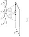
- FIG. 1illustrates how an RFID tag may be coupled to a circuit board during an initial manufacturing stage to help track the manufacturing conditions of the individual circuit board according to one embodiment of the invention.
- FIG. 2illustrates a circuit board including an RFID tag to track and monitor the specific operating conditions and results through various manufacturing stages according to one embodiment of the invention.
- FIG. 4is a block diagram illustrating the flow of information for a collecting and reporting stage-by-stage manufacturing information for a circuit board according to one embodiment of the invention.
- One feature of the inventionprovides for coupling radio frequency identification (RFID) tags to circuit boards to individually help track each circuit board and the manufacturing conditions at various manufacturing stages.
- RFIDradio frequency identification
- Another aspect of the inventionprovides a system that quickly and accurately collects manufacturing information for each item at various manufacturing stages.
- Yet another feature of the inventionprovides a report mechanism for obtaining manufacturing metrics, such as manufacturing conditions, test results, responsible operators, etc., at various manufacturing stages of a particular circuit board.
- FIG. 1illustrates how an RFID tag may be coupled to a circuit board during an initial manufacturing stage to help track the manufacturing conditions of the individual circuit board according to one embodiment of the invention.
- circuit boardincludes, but is not limited to, multi-layer boards, film substrates, flex circuits, multi-chip modules, printed circuit boards, and other types of liquid-laid, flexible, semi-flexible, semi-rigid and/or rigid substrates for forming electrical circuits or having dielectric material.
- Circuit boardstypically undergo various stages of manufacturing, including forming one or more dielectric layers (e.g., resin reinforced layers), forming conductive traces on the circuit board (e.g., etching and plating), forming vias between layers (e.g., drilling holes), mounting electric components on the circuit board, and/or testing of the circuits on the circuit board. These stages involve chemical and/or mechanical processes that may be performed, partially or completely, in an assembly line where the circuit board moves from one stage to another.
- dielectric layerse.g., resin reinforced layers
- conductive traces on the circuit boarde.g., etching and plating
- vias between layerse.g., drilling holes
- a part number 102is typically assigned to a circuit board 104 being manufactured.
- the part number 102may be obtained from a list of instructions describing the board (also known as a shop traveler, routing sheet, job order, or production order) which may also include specific processing requirements for the circuit board 104 .
- the part number 102may be electronically obtained (e.g., from a computer), optically acquired (e.g., by reading a barcode from the traveler), or manually entered by an operator and then transferred to an RFID tag 106 by an RFID writer 110 .
- an identifier(e.g., a serial number for a circuit board) may also be stored in the RFID tag 106 .
- the part number and/or identifiermay be sent by the RFID writer 110 to the RFID tag 106 via radio signals (e.g., directional or omni-directional signal broadcasts), electromagnetic signals, electrical signals (e.g., through direct contacts on the RFID tag 106 ), or other means.
- the RFID tag 106may have an embedded identifier created during the manufacturing of the RFID tag 106 .
- the RFID writer 110is unnecessary.
- the RFID identifiermay simply be read from the RFID tag 106 and then associated with the part number 102 and/or serial number corresponding to the circuit board 104 .
- the part number 102 and/or the identifier stored in the RFID tag 106may be a number, an alpha-numeric code, or symbols.
- the same part number and/or identifiermay be used by a plurality of RFID tags (e.g., a plurality of RFID tags have the same part number to identify a particular group of circuit boards) and/or a unique identifier may be used by each RFID tag (e.g., each number uniquely identifies each circuit board).
- the RFID tag 106may be inserted into an automated optical inspection (AOI) hole in the circuit board 104 .
- AOI holesare typically used in many manufacturing processes for identifying the position and/or orientation of a circuit board.
- Using an AOI hole to hold the RFID tag 106uses an existing feature of circuit board manufacturing process, thereby avoiding having to add new holes, and embeds the RFID tag in a place where it does not interfere with the chemical and/or mechanical processing of the circuit board 104 .
- the RFID tag 106may be protected from mechanical processes, such as pressing or surface planning, is not affected by chemical processes (e.g., etching, plating, etc.), and does not interfere with the manufacturing of the circuit board 104 .
- the RFID tag 106may be coupled (e.g., inserted in an AOI hole) to the circuit board 104 at different stages of manufacturing.
- the RFID tag 106may be coupled to the circuit board 104 at the lay-up stage once a substrate has been formed. If a multilayer circuit board is involved, the RFID tag 106 may be coupled to the circuit board during the formation of the first layer, a middle layer, the last layer, or after the last layer of the multilayer circuit board.
- the RFID tagmay be positioned in a place (e.g., AOI holes) from which it can be removed after the circuit board manufacturing process is completed.
- the RFID tagmay be embedded in a circuit board as it is being made.
- An RFID reader 112may read the part number and/or identifier from the RFID tag 106 using radio signals and provide the part number and/or identifier to a data collector 114 .
- the data collector 114may store this information for later retrieval.
- FIG. 2illustrates a circuit board including an RFID tag 206 to track and monitor the specific operating conditions and results through various manufacturing stages according to one embodiment of the invention.
- the circuit board 204may have been identified and/or associated with the RFID tag 206 coupled to the circuit board 204 at an initial manufacturing stage.
- circuit board 204As the circuit board 204 passes through various manufacturing stages, it is identified by a plurality of RFID readers 208 and 210 . That is, as the circuit board 204 enters or leaves a particular processing stage, an RFID reader 208 or 210 reads a part number and/or identifier from the RFID tag 206 and stores it in a data collector 212 or 214 . In this manner, information about the circuit board's progress can be collected.
- the data collector 212 and 214 at each stagemay also store the date and time in which the RFID tag is read, the name or identifier of the particular stage, the name or number of the operator (if any) responsible for the particular stage, data collected, results, and/or status or the condition of the particular stage. In this manner, the condition, quality, or effectiveness of each manufacturing stage for the circuit board 204 can be obtained. That is, once the RFID tag 206 is read, the part number and/or identifier therein can be associated with the information obtained for each manufacturing stage.
- stages at which a circuit board 204 may be tracked or monitored using its RFID tag 206may include: Prepreg Lay-Up, Pressing, Drilling, Hole Plugging, Dry Film Outerlayer, Plating, Strip-Etch-Strip (SES), Solder Masking, Surface Finishing (including Nickel/Gold, Tin immersion, anti-tarnish (OSP), Silver), Routing, electrical test, Surface Mounting, Final Quality Assurance, etc.
- the circuit board 204may be automatically tracked by one or more RFID readers 208 and 210 as it moves on a conveyor belt from stage to stage and/or manually tracked by an operator presenting the circuit board to an RFID reader 208 and/or 210 at one or more manufacturing stages.
- the RFID tag 312is placed outside the circuit boards 304 , 306 , 308 , and 310 on the perimeter of the substrate 302 .
- the circuit boards 304 , 306 , 308 , and 310are cut away from the substrate 302 prior to delivery leaving the RFID tag 312 behind on the unused frame area.
- the RFID tag 312is not delivered with the circuit boards 304 , 306 , 308 , and 310 .
- a framemay hold one or more circuit boards as they progress through different manufacturing stages with the RFID tag coupled to the frame. Once, the circuit boards are completed, they can be removed from the frame. In either of these embodiments, once manufacturing of the circuit board 304 , 306 , 308 , and 310 on substrate 302 is completed, the RFID tag 312 may be removed and reused with for tracking the manufacture of other circuit boards.
- Another aspect of the inventionprovides for transferring information from the RFID tag 312 to the circuit board(s) 304 , 306 , 308 , and 310 .
- a unique serial number for each circuit board 304 , 306 , 308 , and 310may be generated, possibly, based on the part number and/or identifier in the RFID tag 312 .
- This unique serial numbermay be printed on each circuit board 304 , 306 , 308 , and 310 as a barcode 316 (e.g., 2-dimensional barcode).
- This barcode 316maybe unique to each circuit board 304 , 306 , 308 , and 310 and can be used to later retrieve a stage-by-stage manufacturing report for a particular circuit board.
- This manufacturing reportmay include the processing information, operating conditions, functional and/or quality control test results collected and/or stored during the manufacture of the circuit board.
- the manufacturing reportmay be provided via a web-based application that retrieves the stored information collected from the data collectors at each manufacturing
- AOIautomated optical inspection
- These AOI holes 314are already part of many circuit board manufacturing processes and are typically used by optical sensing machines to identify the position and/or orientation of a circuit board.
- the RFID tag 312may be held completely inside the hole and has a minimal effect on the manufacturing process of the circuit board.
- the RFID tag 312 fitting within an AOI hole 314may have such dimensions that it fits completely within AOI hole 314 .
- the RFID tag 312including the antenna, may be housed in a compact package (e.g., eight millimeter diameter round package, one millimeter thick).
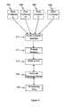
- FIG. 4is a block diagram illustrating the flow of information for a collecting and reporting stage-by-stage manufacturing information for a circuit board according to one embodiment of the invention.
- a plurality of data collectors 402 , 404 , 406 , and 408may collect progress information, test results, operating conditions, and/or compliance status information for each of a plurality of manufacturing stages of a circuit board manufacturing process as illustrated in FIGS. 1 and 2 .
- the data collectors 402 , 404 , 406 , and 408are coupled to a multi-collector interface 410 to transfer the information stored in the data collectors 402 , 404 , 406 , and 408 to a storage database 412 .
- a main server 414may be coupled to the storage database 412 to control access to the information stored in the storage database 412 .
- a manufacturing reportmay be requested via a network reporting server 416 (e.g., internet or web server).
- the network reporting server 416is coupled to the main server 414 to request this stage-by-stage manufacturing information from the storage database 412 .
- the information reported to the requesting customeris not merely limited to order fulfillment information but may also include stage-by-stage information about the manufacturing of circuit board.
- Such stage-by-stage manufacturing informationmay include the dates and times a circuit board has reached and/or finished a stage, the operator responsible for each stage, the operating condition of each stage (e.g., relative or absolute indictor of the effectiveness and/or accuracy of the particular manufacturing stage), the current and past stages reached by a circuit board, the results for each stage, and data for each stage.
- such manufacturing reportmay be obtained after the circuit board has been delivered (e.g., based on a particular circuit board identifier).
- FIG. 5illustrates a sample manufacturing report for a particular circuit board according to one embodiment of the invention.
- FIG. 6is a flow diagram illustrating a method for collecting and reporting stage-by-stage manufacturing information for a circuit board according to one embodiment of the invention.
- An RFID tagis coupled to a circuit board 600 . This may be done at an early stage of manufacturing, for example.
- An identifieris then assigned to the RFID tag 602 . This identifier may be the part number of the circuit board or it may be a unique identifier for each circuit board.
- the RFID tagis scanned and its identifier is recorded 604 .
- the operating conditions or information for each manufacturing stage through which the circuit board is processedare also recorded 606 .
- These operating conditions or informationmay include operator name, date and time each circuit board goes through each stage, test results for each stage, and/or relative or absolute indictors of the effectiveness and/or accuracy of the particular manufacturing stage. If one or more operating conditions fall outside prescribed limits, the system may generate a real-time alert 608 . This alert may serve to warn an operator about a problem with a condition at a particular manufacturing stage.
- the recorded information for the circuit boardis then consolidated or stored in a database 610 . Stage by stage manufacturing information or metrics for the circuit board may be provided, upon request, as a report 612 .
- Employing the RFID tag to track the progress, status, and/or history of each printed circuit board through its manufacturing stagesalso helps to optimize the manufacturing process by identify areas where improved processing would be beneficial.
- This board-by-board trackingalso helps to identify defective circuit boards since they can be more easily identified when they fail a quality control or functional test.
- the tracking systemprovides customers with complete and detailed information about the manufacturing of their circuit boards at every stage of manufacturing. Additionally, a barcode on each circuit board can be used by customers to retrieve a manufacturing report for the circuit board indicating stage-by-stage processing information and whether the circuit board passed all functional and/or quality control tests.
- FIGS. 1 , 2 , 3 , and/or 4may be rearranged and/or combined into a single component or embodied in several components without departing from the invention. Additional elements or components may also be added without departing from the invention.
- the apparatus, devices, and/or components illustrated in FIGS. 1 , 2 , and/or 3may be configured to perform the methods, features, or steps illustrated in FIG. 4 and/or 6 .
Landscapes
- Engineering & Computer Science (AREA)
- General Physics & Mathematics (AREA)
- Physics & Mathematics (AREA)
- Manufacturing & Machinery (AREA)
- Automation & Control Theory (AREA)
- Microelectronics & Electronic Packaging (AREA)
- Theoretical Computer Science (AREA)
- Business, Economics & Management (AREA)
- Quality & Reliability (AREA)
- General Engineering & Computer Science (AREA)
- Tourism & Hospitality (AREA)
- Strategic Management (AREA)
- General Business, Economics & Management (AREA)
- Primary Health Care (AREA)
- Marketing (AREA)
- Artificial Intelligence (AREA)
- Computer Vision & Pattern Recognition (AREA)
- Human Resources & Organizations (AREA)
- General Health & Medical Sciences (AREA)
- Economics (AREA)
- Health & Medical Sciences (AREA)
- Supply And Installment Of Electrical Components (AREA)
- General Factory Administration (AREA)
Abstract
Description
Claims (17)
Priority Applications (8)
| Application Number | Priority Date | Filing Date | Title |
|---|---|---|---|
| US11/336,213US7893833B2 (en) | 2006-01-20 | 2006-01-20 | Inline system for collecting stage-by-stage manufacturing metrics |
| KR1020087020112AKR101294532B1 (en) | 2006-01-20 | 2007-01-18 | Inline system for collecting stage-by-stage manufacturing metrics |
| JP2008551536AJP5312950B2 (en) | 2006-01-20 | 2007-01-18 | Substrates, systems, and methods for collecting step-by-step manufacturing metrics |
| PCT/US2007/060727WO2007084966A2 (en) | 2006-01-20 | 2007-01-18 | Inline system for collecting stage-by-stage manufacturing metrics |
| CN200780008627XACN101401063B (en) | 2006-01-20 | 2007-01-18 | In-Line System for Capturing Step-by-Step Manufacturing Measurements |
| TW096102138ATWI432107B (en) | 2006-01-20 | 2007-01-19 | Inline system for collecting stage-by-stage manufacturing metrics |
| US13/031,217US8188866B2 (en) | 2006-01-20 | 2011-02-20 | Circuit board with radio frequency identification for collecting stage-by-stage manufacturing metrics |
| US13/233,872US8552867B2 (en) | 2006-01-20 | 2011-09-15 | Radio frequency identification for collecting stage-by-stage manufacturing and/or post-manufacturing information associated with a circuit board |
Applications Claiming Priority (1)
| Application Number | Priority Date | Filing Date | Title |
|---|---|---|---|
| US11/336,213US7893833B2 (en) | 2006-01-20 | 2006-01-20 | Inline system for collecting stage-by-stage manufacturing metrics |
Related Child Applications (2)
| Application Number | Title | Priority Date | Filing Date |
|---|---|---|---|
| US13/031,217Continuation-In-PartUS8188866B2 (en) | 2006-01-20 | 2011-02-20 | Circuit board with radio frequency identification for collecting stage-by-stage manufacturing metrics |
| US13/031,217ContinuationUS8188866B2 (en) | 2006-01-20 | 2011-02-20 | Circuit board with radio frequency identification for collecting stage-by-stage manufacturing metrics |
Publications (2)
| Publication Number | Publication Date |
|---|---|
| US20070173970A1 US20070173970A1 (en) | 2007-07-26 |
| US7893833B2true US7893833B2 (en) | 2011-02-22 |
Family
ID=38286544
Family Applications (2)
| Application Number | Title | Priority Date | Filing Date |
|---|---|---|---|
| US11/336,213Active2029-11-23US7893833B2 (en) | 2006-01-20 | 2006-01-20 | Inline system for collecting stage-by-stage manufacturing metrics |
| US13/031,217ActiveUS8188866B2 (en) | 2006-01-20 | 2011-02-20 | Circuit board with radio frequency identification for collecting stage-by-stage manufacturing metrics |
Family Applications After (1)
| Application Number | Title | Priority Date | Filing Date |
|---|---|---|---|
| US13/031,217ActiveUS8188866B2 (en) | 2006-01-20 | 2011-02-20 | Circuit board with radio frequency identification for collecting stage-by-stage manufacturing metrics |
Country Status (6)
| Country | Link |
|---|---|
| US (2) | US7893833B2 (en) |
| JP (1) | JP5312950B2 (en) |
| KR (1) | KR101294532B1 (en) |
| CN (1) | CN101401063B (en) |
| TW (1) | TWI432107B (en) |
| WO (1) | WO2007084966A2 (en) |
Cited By (2)
| Publication number | Priority date | Publication date | Assignee | Title |
|---|---|---|---|---|
| US20120261477A1 (en)* | 2006-06-21 | 2012-10-18 | Neology, Inc. | Systems and methods for breakaway rfid tags |
| US10930535B2 (en)* | 2016-12-02 | 2021-02-23 | Applied Materials, Inc. | RFID part authentication and tracking of processing components |
Families Citing this family (30)
| Publication number | Priority date | Publication date | Assignee | Title |
|---|---|---|---|---|
| US9083781B2 (en) | 2004-11-15 | 2015-07-14 | Bascule Development Ag Llc | Portable image-capturing device with embedded projector |
| US20070050075A1 (en)* | 2005-08-26 | 2007-03-01 | Electro Scientific Industries, Inc. | Automatic wafer tracking process and apparatus for carrying out the process |
| US20080104117A1 (en)* | 2006-10-19 | 2008-05-01 | Visible Assets, Inc. | Radio-Networked Welder System |
| DE102008021750A1 (en)* | 2008-04-30 | 2009-11-05 | Endress + Hauser Gmbh + Co. Kg | Contactlessly identifiable electronic printed circuit board for measuring device, has radio frequency identification transponder inserted into recess, and electronic component comprising connection soldered on contact surface |
| GB2460071A (en)* | 2008-05-15 | 2009-11-18 | Lyncolec Ltd | Printed Circuit Board Including a RFID device |
| EP2141970A1 (en)* | 2008-06-30 | 2010-01-06 | Elfab AG Eletronikfabrikation | Circuit board with an RFID chip for traceability and method for producing such a circuit board |
| JP2010027665A (en)* | 2008-07-15 | 2010-02-04 | Alps Electric Co Ltd | Method of manufacturing ceramic multilayered wiring board, and ceramic multilayered wiring board |
| JP5257238B2 (en)* | 2009-05-21 | 2013-08-07 | 大日本印刷株式会社 | Manufacturing information management method for printed wiring board, manufacturing information management system for printed wiring board |
| TW201134332A (en)* | 2010-03-16 | 2011-10-01 | Ind Tech Res Inst | Printed circuit board with embedded antenna for RFID tag and method for manufacturing the same |
| US20170118880A1 (en)* | 2010-03-24 | 2017-04-27 | Duetto Integrated Systems, Inc. | Supplemental lighting for reading information on circuit boards for use with a bond head assembly system |
| US9210307B2 (en)* | 2010-11-04 | 2015-12-08 | Magna Electronics, Inc. | Vehicular camera system with reduced number of pins and conduits |
| CN102324050B (en)* | 2011-04-19 | 2015-04-15 | 佛山市瑞德软件科技有限公司 | Method and dedicated device for recording information of home appliance controller by using RFID (Radio Frequency Identification Device) chip |
| EP2748769B1 (en) | 2011-08-23 | 2018-04-18 | eAGILE, INC. | System for associating rfid tag with upc code, and validating associative encoding of same |
| US20130194076A1 (en)* | 2012-01-30 | 2013-08-01 | Yu-Min Ho | Process Monitoring System and Related Method |
| US20150073581A1 (en)* | 2013-09-11 | 2015-03-12 | Advanced Consulting Services Corp. | System for reducing energy consumption and fraction defective when producing pcb based on ubiquitous sensor network |
| KR101490936B1 (en)* | 2013-12-05 | 2015-02-06 | 현대자동차 주식회사 | Inspection system control method for vehicle |
| CN103945684B (en)* | 2014-04-14 | 2017-06-20 | 肖根福罗格注胶技术(苏州工业园区)有限公司 | A kind of assembling device of PCB |
| TW201545819A (en)* | 2014-06-06 | 2015-12-16 | Yealy Optic Electronic Co Ltd | Computer vision identification output image assisted led die selection system and selection method |
| CN107666978B (en)* | 2015-06-05 | 2020-07-31 | 格里森刀具股份有限公司 | Tool with removable information device |
| DE102016102135B3 (en)* | 2016-02-08 | 2017-08-03 | Asm Assembly Systems Gmbh & Co. Kg | PCB - transport system and manufacturing system |
| WO2018165146A1 (en) | 2017-03-06 | 2018-09-13 | Cummins Filtration Ip, Inc. | Genuine filter recognition with filter monitoring system |
| WO2019077676A1 (en)* | 2017-10-17 | 2019-04-25 | 株式会社Fuji | Machining tool apparatus |
| CN110321749B (en)* | 2018-03-28 | 2022-05-13 | 奥特斯(中国)有限公司 | Dual code traceable system for a component carrier |
| CN108830347B (en)* | 2018-05-31 | 2022-03-22 | Oppo广东移动通信有限公司 | Circuit board tracking management method, device and electronic equipment |
| US20200385824A1 (en)* | 2019-06-10 | 2020-12-10 | Apdn (B.V.I.) Inc. | Dna marking of leather |
| EP4043971A4 (en) | 2019-10-11 | 2022-11-16 | Panasonic Intellectual Property Management Co., Ltd. | Identifier management method, and reading device |
| US11481520B2 (en) | 2020-12-15 | 2022-10-25 | Hewlett Packard Enterprise Development Lp | Secure identification of a printed circuit board |
| EP4267263A4 (en)* | 2020-12-23 | 2024-11-20 | Helios Sports, Inc. | TRAINING SYSTEMS AND METHODS FOR ASSOCIATE HOCKEY |
| DE102021117346A1 (en)* | 2021-07-06 | 2023-01-12 | Bayerische Motoren Werke Aktiengesellschaft | Process for operating a press, computer program and electronically readable data carrier |
| DE102022125639A1 (en)* | 2022-10-05 | 2024-04-11 | ASMPT GmbH & Co. KG | RFID module for a placement machine |
Citations (8)
| Publication number | Priority date | Publication date | Assignee | Title |
|---|---|---|---|---|
| US5787174A (en) | 1992-06-17 | 1998-07-28 | Micron Technology, Inc. | Remote identification of integrated circuit |
| US6486780B1 (en) | 1998-08-14 | 2002-11-26 | 3M Innovative Properties Company | Applications for radio frequency identification systems |
| US20030102367A1 (en) | 2000-04-20 | 2003-06-05 | Francois Monette | Automated manufacturing control system |
| US6714121B1 (en) | 1999-08-09 | 2004-03-30 | Micron Technology, Inc. | RFID material tracking method and apparatus |
| US6909356B2 (en) | 2000-11-03 | 2005-06-21 | Seecontrol, Inc. | Method and apparatus for associating the movement of goods with the identity of an individual moving the goods |
| US20050178811A1 (en) | 2004-02-18 | 2005-08-18 | Honeywell International, Inc. | Wireless inventory re-ordering system for surface mount technology pick and place assembly machines |
| US20050242953A1 (en)* | 2003-10-24 | 2005-11-03 | Toshiba Teli Corporation | Object tagged with RFID tag and device and method for processing it |
| US7665661B2 (en)* | 2005-03-28 | 2010-02-23 | R828 Llc | Secure system for tracking elements using tags |
Family Cites Families (10)
| Publication number | Priority date | Publication date | Assignee | Title |
|---|---|---|---|---|
| JPH04179184A (en)* | 1990-11-09 | 1992-06-25 | Hitachi Ltd | Printed wiring board and its manufacturing method |
| JP2000357847A (en)* | 1999-06-15 | 2000-12-26 | Tohken Co Ltd | Printed circuit board with ID tag and method of recognizing process of distribution of printed circuit board |
| US6883710B2 (en) | 2000-10-11 | 2005-04-26 | Amerasia International Technology, Inc. | Article tracking system and method |
| JP4254183B2 (en)* | 2002-09-17 | 2009-04-15 | 株式会社デンソー | Printed wiring board and printed wiring board management system |
| US7093756B2 (en)* | 2002-10-31 | 2006-08-22 | Sap Aktiengesellschaft | Distributed production control |
| JP3992108B2 (en)* | 2003-11-28 | 2007-10-17 | 松下電器産業株式会社 | Circuit board production method and data processing method |
| JP2005228774A (en)* | 2004-02-10 | 2005-08-25 | Shinden Hightex Kk | Method of manufacturing printed circuit board |
| CN1713221A (en)* | 2004-06-25 | 2005-12-28 | 黄胜昌 | RFID In-Mold Formed Labels |
| US20060109119A1 (en)* | 2004-11-19 | 2006-05-25 | Jeremy Burr | RFID tag in a printed circuit board |
| US8072326B2 (en) | 2005-06-29 | 2011-12-06 | Martin Cotton | Tamperproof RFID component integrated into a multilayer printed circuit board |
- 2006
- 2006-01-20USUS11/336,213patent/US7893833B2/enactiveActive
- 2007
- 2007-01-18JPJP2008551536Apatent/JP5312950B2/enactiveActive
- 2007-01-18CNCN200780008627XApatent/CN101401063B/enactiveActive
- 2007-01-18WOPCT/US2007/060727patent/WO2007084966A2/enactiveApplication Filing
- 2007-01-18KRKR1020087020112Apatent/KR101294532B1/enactiveActive
- 2007-01-19TWTW096102138Apatent/TWI432107B/enactive
- 2011
- 2011-02-20USUS13/031,217patent/US8188866B2/enactiveActive
Patent Citations (9)
| Publication number | Priority date | Publication date | Assignee | Title |
|---|---|---|---|---|
| US5787174A (en) | 1992-06-17 | 1998-07-28 | Micron Technology, Inc. | Remote identification of integrated circuit |
| US6486780B1 (en) | 1998-08-14 | 2002-11-26 | 3M Innovative Properties Company | Applications for radio frequency identification systems |
| US6768419B2 (en) | 1998-08-14 | 2004-07-27 | 3M Innovative Properties Company | Applications for radio frequency identification systems |
| US6714121B1 (en) | 1999-08-09 | 2004-03-30 | Micron Technology, Inc. | RFID material tracking method and apparatus |
| US20030102367A1 (en) | 2000-04-20 | 2003-06-05 | Francois Monette | Automated manufacturing control system |
| US6909356B2 (en) | 2000-11-03 | 2005-06-21 | Seecontrol, Inc. | Method and apparatus for associating the movement of goods with the identity of an individual moving the goods |
| US20050242953A1 (en)* | 2003-10-24 | 2005-11-03 | Toshiba Teli Corporation | Object tagged with RFID tag and device and method for processing it |
| US20050178811A1 (en) | 2004-02-18 | 2005-08-18 | Honeywell International, Inc. | Wireless inventory re-ordering system for surface mount technology pick and place assembly machines |
| US7665661B2 (en)* | 2005-03-28 | 2010-02-23 | R828 Llc | Secure system for tracking elements using tags |
Cited By (14)
| Publication number | Priority date | Publication date | Assignee | Title |
|---|---|---|---|---|
| US20120261477A1 (en)* | 2006-06-21 | 2012-10-18 | Neology, Inc. | Systems and methods for breakaway rfid tags |
| US8610580B2 (en)* | 2006-06-21 | 2013-12-17 | Neology, Inc. | Systems and methods for breakaway RFID tags |
| US8669874B2 (en) | 2006-06-21 | 2014-03-11 | Neology, Inc. | Systems and methods for stirring electromagnetic fields and interrogating stationary RFID tags |
| US8680973B2 (en) | 2006-06-21 | 2014-03-25 | Neology, Inc. | Systems and methods for synchronizing a plurality of RFID interrogators in a theatre of operation |
| US8991714B2 (en) | 2006-06-21 | 2015-03-31 | Neology, Inc. | Systems and methods for breakaway RFID tags |
| US9247634B2 (en) | 2006-06-21 | 2016-01-26 | Neology, Inc. | Systems and methods for synchronizing a plurality of RFID interrogators in a theatre of operation |
| US9253876B2 (en) | 2006-06-21 | 2016-02-02 | Neology, Inc. | Systems and methods for breakaway RFID tags |
| US9501736B2 (en) | 2006-06-21 | 2016-11-22 | Neology, Inc. | Systems and methods for breakaway RFID tags |
| US9626619B2 (en) | 2006-06-21 | 2017-04-18 | Neology, Inc. | Systems and methods for synchronizing a plurality of RFID interrogators in a theatre of operation |
| US9747542B2 (en) | 2006-06-21 | 2017-08-29 | Neology, Inc. | Systems and methods for breakaway RFID tags |
| US10133894B2 (en) | 2006-06-21 | 2018-11-20 | Smartac Technology Fletcher, Inc. | Systems and methods for stirring electromagnetic fields and interrogating stationary RFID tags |
| US10235545B2 (en) | 2006-06-21 | 2019-03-19 | Smartrac Technology Fletcher, Inc. | Systems and methods for synchronizing a plurality of RFID interrogators in a theatre of operation |
| US10930535B2 (en)* | 2016-12-02 | 2021-02-23 | Applied Materials, Inc. | RFID part authentication and tracking of processing components |
| US11848220B2 (en) | 2016-12-02 | 2023-12-19 | Applied Materials, Inc. | RFID part authentication and tracking of processing components |
Also Published As
| Publication number | Publication date |
|---|---|
| TW200738081A (en) | 2007-10-01 |
| US20070173970A1 (en) | 2007-07-26 |
| KR20080100194A (en) | 2008-11-14 |
| US20110133899A1 (en) | 2011-06-09 |
| KR101294532B1 (en) | 2013-08-07 |
| WO2007084966A3 (en) | 2008-04-10 |
| CN101401063B (en) | 2012-07-18 |
| US8188866B2 (en) | 2012-05-29 |
| JP2009524256A (en) | 2009-06-25 |
| JP5312950B2 (en) | 2013-10-09 |
| CN101401063A (en) | 2009-04-01 |
| TWI432107B (en) | 2014-03-21 |
| WO2007084966A2 (en) | 2007-07-26 |
Similar Documents
| Publication | Publication Date | Title |
|---|---|---|
| US7893833B2 (en) | Inline system for collecting stage-by-stage manufacturing metrics | |
| US8552867B2 (en) | Radio frequency identification for collecting stage-by-stage manufacturing and/or post-manufacturing information associated with a circuit board | |
| JP5647192B2 (en) | Apparatus and method for automatic marking of defects on a web of material | |
| US8610580B2 (en) | Systems and methods for breakaway RFID tags | |
| KR100599361B1 (en) | Record medium recording quality control system, quality control method and quality control program | |
| CN109923955B (en) | Reclassification system and reclassification method for saving images | |
| EP1755073A2 (en) | RFID inlays and methods of their manufacture | |
| US20060038687A1 (en) | Singulation of radio frequency identification (RFID) tags for testing and/or programming | |
| CN113508348A (en) | Method and computing device for tracking components in a production line including multiple process equipment | |
| JP2009538530A (en) | Embedded inspection image archive for electronic assembly machines | |
| WO2021250679A1 (en) | System and method for tracing components of electronic assembly | |
| WO2022078887A1 (en) | Test target defect identification and evaluation for assessing quality of component carrier structure | |
| CN111260378A (en) | MES-based quality tracing method and system | |
| WO2022078891A1 (en) | Coupon for testing quality of related component carriers by automated quality test apparatus | |
| US20050274802A1 (en) | Circuit board inspection apparatus | |
| CN101300473A (en) | Verification of non-recurring defects in pattern inspection | |
| JP2012204455A (en) | Mounting failure analysis system and process abnormality monitoring system | |
| CN109964277A (en) | For detecting and removing the method and apparatus of defective integrated antenna package | |
| KR101408848B1 (en) | Information tracing method of pcb test processing with multi-step mapping | |
| JP2001007480A (en) | Method for managing multilayer printed circuit board | |
| CN114331262A (en) | Printed circuit board manufacturing full-flow tracing system with informationized identification, reading, operation, storage and datamation output | |
| JP4446845B2 (en) | Printed circuit board manufacturing method and manufacturing apparatus | |
| CN101212857B (en) | Printed circuit board capable of identifying production information | |
| JP5257238B2 (en) | Manufacturing information management method for printed wiring board, manufacturing information management system for printed wiring board | |
| JP6503813B2 (en) | Identification device, identification method and traceability system |
Legal Events
| Date | Code | Title | Description |
|---|---|---|---|
| AS | Assignment | Owner name:SANMINA-SCI CORPORATION, CALIFORNIA Free format text:ASSIGNMENT OF ASSIGNORS INTEREST;ASSIGNOR:SHACHAR, RONY;REEL/FRAME:017489/0308 Effective date:20060112 | |
| STCF | Information on status: patent grant | Free format text:PATENTED CASE | |
| AS | Assignment | Owner name:US BANK NATIONAL ASSOCIATION, AS NOTES COLLATERAL Free format text:SECURITY INTEREST;ASSIGNORS:SANMINA CORPORATION, AS GRANTOR;SANMINA CORPORATION, F/K/A SANMINA-SCI CORPORATION, AS GRANTOR;HADCO SANTA CLARA, INC., AS GRANTOR;AND OTHERS;REEL/FRAME:033094/0826 Effective date:20140604 | |
| FPAY | Fee payment | Year of fee payment:4 | |
| MAFP | Maintenance fee payment | Free format text:PAYMENT OF MAINTENANCE FEE, 8TH YEAR, LARGE ENTITY (ORIGINAL EVENT CODE: M1552) Year of fee payment:8 | |
| AS | Assignment | Owner name:HADCO SANTA CLARA, CALIFORNIA Free format text:RELEASE BY SECURED PARTY;ASSIGNOR:U.S. BANK NATIONAL ASSOCIATION, SOLELY AS NOTES COLLATERAL AGENT;REEL/FRAME:049378/0927 Effective date:20190531 Owner name:SCI TECHNOLOGY, CALIFORNIA Free format text:RELEASE BY SECURED PARTY;ASSIGNOR:U.S. BANK NATIONAL ASSOCIATION, SOLELY AS NOTES COLLATERAL AGENT;REEL/FRAME:049378/0927 Effective date:20190531 Owner name:SENSORWISE, INC., CALIFORNIA Free format text:RELEASE BY SECURED PARTY;ASSIGNOR:U.S. BANK NATIONAL ASSOCIATION, SOLELY AS NOTES COLLATERAL AGENT;REEL/FRAME:049378/0927 Effective date:20190531 Owner name:HADCO CORPORATION, CALIFORNIA Free format text:RELEASE BY SECURED PARTY;ASSIGNOR:U.S. BANK NATIONAL ASSOCIATION, SOLELY AS NOTES COLLATERAL AGENT;REEL/FRAME:049378/0927 Effective date:20190531 Owner name:SANMINA CORPORATION, CALIFORNIA Free format text:RELEASE BY SECURED PARTY;ASSIGNOR:U.S. BANK NATIONAL ASSOCIATION, SOLELY AS NOTES COLLATERAL AGENT;REEL/FRAME:049378/0927 Effective date:20190531 | |
| MAFP | Maintenance fee payment | Free format text:PAYMENT OF MAINTENANCE FEE, 12TH YEAR, LARGE ENTITY (ORIGINAL EVENT CODE: M1553); ENTITY STATUS OF PATENT OWNER: LARGE ENTITY Year of fee payment:12 |