US7893546B2 - Ball grid array package enhanced with a thermal and electrical connector - Google Patents
Ball grid array package enhanced with a thermal and electrical connectorDownload PDFInfo
- Publication number
- US7893546B2 US7893546B2US12/260,784US26078408AUS7893546B2US 7893546 B2US7893546 B2US 7893546B2US 26078408 AUS26078408 AUS 26078408AUS 7893546 B2US7893546 B2US 7893546B2
- Authority
- US
- United States
- Prior art keywords
- substrate
- stiffener
- die
- pcb
- thermal
- Prior art date
- Legal status (The legal status is an assumption and is not a legal conclusion. Google has not performed a legal analysis and makes no representation as to the accuracy of the status listed.)
- Expired - Fee Related
Links
Images


Classifications
- H—ELECTRICITY
- H01—ELECTRIC ELEMENTS
- H01L—SEMICONDUCTOR DEVICES NOT COVERED BY CLASS H10
- H01L23/00—Details of semiconductor or other solid state devices
- H01L23/34—Arrangements for cooling, heating, ventilating or temperature compensation ; Temperature sensing arrangements
- H01L23/36—Selection of materials, or shaping, to facilitate cooling or heating, e.g. heatsinks
- H01L23/373—Cooling facilitated by selection of materials for the device or materials for thermal expansion adaptation, e.g. carbon
- H01L23/3735—Laminates or multilayers, e.g. direct bond copper ceramic substrates
- H—ELECTRICITY
- H01—ELECTRIC ELEMENTS
- H01L—SEMICONDUCTOR DEVICES NOT COVERED BY CLASS H10
- H01L23/00—Details of semiconductor or other solid state devices
- H01L23/16—Fillings or auxiliary members in containers or encapsulations, e.g. centering rings
- H—ELECTRICITY
- H01—ELECTRIC ELEMENTS
- H01L—SEMICONDUCTOR DEVICES NOT COVERED BY CLASS H10
- H01L23/00—Details of semiconductor or other solid state devices
- H01L23/16—Fillings or auxiliary members in containers or encapsulations, e.g. centering rings
- H01L23/18—Fillings characterised by the material, its physical or chemical properties, or its arrangement within the complete device
- H01L23/24—Fillings characterised by the material, its physical or chemical properties, or its arrangement within the complete device solid or gel at the normal operating temperature of the device
- H—ELECTRICITY
- H01—ELECTRIC ELEMENTS
- H01L—SEMICONDUCTOR DEVICES NOT COVERED BY CLASS H10
- H01L23/00—Details of semiconductor or other solid state devices
- H01L23/28—Encapsulations, e.g. encapsulating layers, coatings, e.g. for protection
- H01L23/31—Encapsulations, e.g. encapsulating layers, coatings, e.g. for protection characterised by the arrangement or shape
- H01L23/3107—Encapsulations, e.g. encapsulating layers, coatings, e.g. for protection characterised by the arrangement or shape the device being completely enclosed
- H01L23/3121—Encapsulations, e.g. encapsulating layers, coatings, e.g. for protection characterised by the arrangement or shape the device being completely enclosed a substrate forming part of the encapsulation
- H01L23/3128—Encapsulations, e.g. encapsulating layers, coatings, e.g. for protection characterised by the arrangement or shape the device being completely enclosed a substrate forming part of the encapsulation the substrate having spherical bumps for external connection
- H—ELECTRICITY
- H01—ELECTRIC ELEMENTS
- H01L—SEMICONDUCTOR DEVICES NOT COVERED BY CLASS H10
- H01L23/00—Details of semiconductor or other solid state devices
- H01L23/34—Arrangements for cooling, heating, ventilating or temperature compensation ; Temperature sensing arrangements
- H01L23/36—Selection of materials, or shaping, to facilitate cooling or heating, e.g. heatsinks
- H01L23/367—Cooling facilitated by shape of device
- H01L23/3677—Wire-like or pin-like cooling fins or heat sinks
- H—ELECTRICITY
- H01—ELECTRIC ELEMENTS
- H01L—SEMICONDUCTOR DEVICES NOT COVERED BY CLASS H10
- H01L23/00—Details of semiconductor or other solid state devices
- H01L23/34—Arrangements for cooling, heating, ventilating or temperature compensation ; Temperature sensing arrangements
- H01L23/42—Fillings or auxiliary members in containers or encapsulations selected or arranged to facilitate heating or cooling
- H01L23/433—Auxiliary members in containers characterised by their shape, e.g. pistons
- H01L23/4334—Auxiliary members in encapsulations
- H—ELECTRICITY
- H01—ELECTRIC ELEMENTS
- H01L—SEMICONDUCTOR DEVICES NOT COVERED BY CLASS H10
- H01L23/00—Details of semiconductor or other solid state devices
- H01L23/48—Arrangements for conducting electric current to or from the solid state body in operation, e.g. leads, terminal arrangements ; Selection of materials therefor
- H01L23/488—Arrangements for conducting electric current to or from the solid state body in operation, e.g. leads, terminal arrangements ; Selection of materials therefor consisting of soldered or bonded constructions
- H01L23/498—Leads, i.e. metallisations or lead-frames on insulating substrates, e.g. chip carriers
- H01L23/49833—Leads, i.e. metallisations or lead-frames on insulating substrates, e.g. chip carriers the chip support structure consisting of a plurality of insulating substrates
- H—ELECTRICITY
- H01—ELECTRIC ELEMENTS
- H01L—SEMICONDUCTOR DEVICES NOT COVERED BY CLASS H10
- H01L24/00—Arrangements for connecting or disconnecting semiconductor or solid-state bodies; Methods or apparatus related thereto
- H01L24/01—Means for bonding being attached to, or being formed on, the surface to be connected, e.g. chip-to-package, die-attach, "first-level" interconnects; Manufacturing methods related thereto
- H01L24/42—Wire connectors; Manufacturing methods related thereto
- H01L24/47—Structure, shape, material or disposition of the wire connectors after the connecting process
- H01L24/49—Structure, shape, material or disposition of the wire connectors after the connecting process of a plurality of wire connectors
- H—ELECTRICITY
- H01—ELECTRIC ELEMENTS
- H01L—SEMICONDUCTOR DEVICES NOT COVERED BY CLASS H10
- H01L2224/00—Indexing scheme for arrangements for connecting or disconnecting semiconductor or solid-state bodies and methods related thereto as covered by H01L24/00
- H01L2224/01—Means for bonding being attached to, or being formed on, the surface to be connected, e.g. chip-to-package, die-attach, "first-level" interconnects; Manufacturing methods related thereto
- H01L2224/02—Bonding areas; Manufacturing methods related thereto
- H01L2224/04—Structure, shape, material or disposition of the bonding areas prior to the connecting process
- H01L2224/0401—Bonding areas specifically adapted for bump connectors, e.g. under bump metallisation [UBM]
- H—ELECTRICITY
- H01—ELECTRIC ELEMENTS
- H01L—SEMICONDUCTOR DEVICES NOT COVERED BY CLASS H10
- H01L2224/00—Indexing scheme for arrangements for connecting or disconnecting semiconductor or solid-state bodies and methods related thereto as covered by H01L24/00
- H01L2224/01—Means for bonding being attached to, or being formed on, the surface to be connected, e.g. chip-to-package, die-attach, "first-level" interconnects; Manufacturing methods related thereto
- H01L2224/02—Bonding areas; Manufacturing methods related thereto
- H01L2224/04—Structure, shape, material or disposition of the bonding areas prior to the connecting process
- H01L2224/05—Structure, shape, material or disposition of the bonding areas prior to the connecting process of an individual bonding area
- H01L2224/0554—External layer
- H01L2224/05599—Material
- H01L2224/056—Material with a principal constituent of the material being a metal or a metalloid, e.g. boron [B], silicon [Si], germanium [Ge], arsenic [As], antimony [Sb], tellurium [Te] and polonium [Po], and alloys thereof
- H01L2224/05617—Material with a principal constituent of the material being a metal or a metalloid, e.g. boron [B], silicon [Si], germanium [Ge], arsenic [As], antimony [Sb], tellurium [Te] and polonium [Po], and alloys thereof the principal constituent melting at a temperature of greater than or equal to 400°C and less than 950°C
- H01L2224/05624—Aluminium [Al] as principal constituent
- H—ELECTRICITY
- H01—ELECTRIC ELEMENTS
- H01L—SEMICONDUCTOR DEVICES NOT COVERED BY CLASS H10
- H01L2224/00—Indexing scheme for arrangements for connecting or disconnecting semiconductor or solid-state bodies and methods related thereto as covered by H01L24/00
- H01L2224/01—Means for bonding being attached to, or being formed on, the surface to be connected, e.g. chip-to-package, die-attach, "first-level" interconnects; Manufacturing methods related thereto
- H01L2224/26—Layer connectors, e.g. plate connectors, solder or adhesive layers; Manufacturing methods related thereto
- H01L2224/28—Structure, shape, material or disposition of the layer connectors prior to the connecting process
- H01L2224/29—Structure, shape, material or disposition of the layer connectors prior to the connecting process of an individual layer connector
- H01L2224/29001—Core members of the layer connector
- H01L2224/29099—Material
- H01L2224/29198—Material with a principal constituent of the material being a combination of two or more materials in the form of a matrix with a filler, i.e. being a hybrid material, e.g. segmented structures, foams
- H01L2224/29199—Material of the matrix
- H01L2224/2929—Material of the matrix with a principal constituent of the material being a polymer, e.g. polyester, phenolic based polymer, epoxy
- H—ELECTRICITY
- H01—ELECTRIC ELEMENTS
- H01L—SEMICONDUCTOR DEVICES NOT COVERED BY CLASS H10
- H01L2224/00—Indexing scheme for arrangements for connecting or disconnecting semiconductor or solid-state bodies and methods related thereto as covered by H01L24/00
- H01L2224/01—Means for bonding being attached to, or being formed on, the surface to be connected, e.g. chip-to-package, die-attach, "first-level" interconnects; Manufacturing methods related thereto
- H01L2224/26—Layer connectors, e.g. plate connectors, solder or adhesive layers; Manufacturing methods related thereto
- H01L2224/28—Structure, shape, material or disposition of the layer connectors prior to the connecting process
- H01L2224/29—Structure, shape, material or disposition of the layer connectors prior to the connecting process of an individual layer connector
- H01L2224/29001—Core members of the layer connector
- H01L2224/29099—Material
- H01L2224/29198—Material with a principal constituent of the material being a combination of two or more materials in the form of a matrix with a filler, i.e. being a hybrid material, e.g. segmented structures, foams
- H01L2224/29298—Fillers
- H01L2224/29299—Base material
- H01L2224/293—Base material with a principal constituent of the material being a metal or a metalloid, e.g. boron [B], silicon [Si], germanium [Ge], arsenic [As], antimony [Sb], tellurium [Te] and polonium [Po], and alloys thereof
- H01L2224/29338—Base material with a principal constituent of the material being a metal or a metalloid, e.g. boron [B], silicon [Si], germanium [Ge], arsenic [As], antimony [Sb], tellurium [Te] and polonium [Po], and alloys thereof the principal constituent melting at a temperature of greater than or equal to 950°C and less than 1550°C
- H01L2224/29339—Silver [Ag] as principal constituent
- H—ELECTRICITY
- H01—ELECTRIC ELEMENTS
- H01L—SEMICONDUCTOR DEVICES NOT COVERED BY CLASS H10
- H01L2224/00—Indexing scheme for arrangements for connecting or disconnecting semiconductor or solid-state bodies and methods related thereto as covered by H01L24/00
- H01L2224/01—Means for bonding being attached to, or being formed on, the surface to be connected, e.g. chip-to-package, die-attach, "first-level" interconnects; Manufacturing methods related thereto
- H01L2224/26—Layer connectors, e.g. plate connectors, solder or adhesive layers; Manufacturing methods related thereto
- H01L2224/31—Structure, shape, material or disposition of the layer connectors after the connecting process
- H01L2224/32—Structure, shape, material or disposition of the layer connectors after the connecting process of an individual layer connector
- H01L2224/321—Disposition
- H01L2224/32151—Disposition the layer connector connecting between a semiconductor or solid-state body and an item not being a semiconductor or solid-state body, e.g. chip-to-substrate, chip-to-passive
- H01L2224/32153—Disposition the layer connector connecting between a semiconductor or solid-state body and an item not being a semiconductor or solid-state body, e.g. chip-to-substrate, chip-to-passive the body and the item being arranged next to each other, e.g. on a common substrate
- H01L2224/32175—Disposition the layer connector connecting between a semiconductor or solid-state body and an item not being a semiconductor or solid-state body, e.g. chip-to-substrate, chip-to-passive the body and the item being arranged next to each other, e.g. on a common substrate the item being metallic
- H01L2224/32188—Disposition the layer connector connecting between a semiconductor or solid-state body and an item not being a semiconductor or solid-state body, e.g. chip-to-substrate, chip-to-passive the body and the item being arranged next to each other, e.g. on a common substrate the item being metallic the layer connector connecting to a bonding area protruding from the surface of the item
- H—ELECTRICITY
- H01—ELECTRIC ELEMENTS
- H01L—SEMICONDUCTOR DEVICES NOT COVERED BY CLASS H10
- H01L2224/00—Indexing scheme for arrangements for connecting or disconnecting semiconductor or solid-state bodies and methods related thereto as covered by H01L24/00
- H01L2224/01—Means for bonding being attached to, or being formed on, the surface to be connected, e.g. chip-to-package, die-attach, "first-level" interconnects; Manufacturing methods related thereto
- H01L2224/26—Layer connectors, e.g. plate connectors, solder or adhesive layers; Manufacturing methods related thereto
- H01L2224/31—Structure, shape, material or disposition of the layer connectors after the connecting process
- H01L2224/32—Structure, shape, material or disposition of the layer connectors after the connecting process of an individual layer connector
- H01L2224/321—Disposition
- H01L2224/32151—Disposition the layer connector connecting between a semiconductor or solid-state body and an item not being a semiconductor or solid-state body, e.g. chip-to-substrate, chip-to-passive
- H01L2224/32221—Disposition the layer connector connecting between a semiconductor or solid-state body and an item not being a semiconductor or solid-state body, e.g. chip-to-substrate, chip-to-passive the body and the item being stacked
- H01L2224/32225—Disposition the layer connector connecting between a semiconductor or solid-state body and an item not being a semiconductor or solid-state body, e.g. chip-to-substrate, chip-to-passive the body and the item being stacked the item being non-metallic, e.g. insulating substrate with or without metallisation
- H—ELECTRICITY
- H01—ELECTRIC ELEMENTS
- H01L—SEMICONDUCTOR DEVICES NOT COVERED BY CLASS H10
- H01L2224/00—Indexing scheme for arrangements for connecting or disconnecting semiconductor or solid-state bodies and methods related thereto as covered by H01L24/00
- H01L2224/01—Means for bonding being attached to, or being formed on, the surface to be connected, e.g. chip-to-package, die-attach, "first-level" interconnects; Manufacturing methods related thereto
- H01L2224/42—Wire connectors; Manufacturing methods related thereto
- H01L2224/44—Structure, shape, material or disposition of the wire connectors prior to the connecting process
- H01L2224/45—Structure, shape, material or disposition of the wire connectors prior to the connecting process of an individual wire connector
- H01L2224/45001—Core members of the connector
- H01L2224/45099—Material
- H01L2224/451—Material with a principal constituent of the material being a metal or a metalloid, e.g. boron (B), silicon (Si), germanium (Ge), arsenic (As), antimony (Sb), tellurium (Te) and polonium (Po), and alloys thereof
- H01L2224/45117—Material with a principal constituent of the material being a metal or a metalloid, e.g. boron (B), silicon (Si), germanium (Ge), arsenic (As), antimony (Sb), tellurium (Te) and polonium (Po), and alloys thereof the principal constituent melting at a temperature of greater than or equal to 400°C and less than 950°C
- H01L2224/45124—Aluminium (Al) as principal constituent
- H—ELECTRICITY
- H01—ELECTRIC ELEMENTS
- H01L—SEMICONDUCTOR DEVICES NOT COVERED BY CLASS H10
- H01L2224/00—Indexing scheme for arrangements for connecting or disconnecting semiconductor or solid-state bodies and methods related thereto as covered by H01L24/00
- H01L2224/01—Means for bonding being attached to, or being formed on, the surface to be connected, e.g. chip-to-package, die-attach, "first-level" interconnects; Manufacturing methods related thereto
- H01L2224/42—Wire connectors; Manufacturing methods related thereto
- H01L2224/44—Structure, shape, material or disposition of the wire connectors prior to the connecting process
- H01L2224/45—Structure, shape, material or disposition of the wire connectors prior to the connecting process of an individual wire connector
- H01L2224/45001—Core members of the connector
- H01L2224/45099—Material
- H01L2224/451—Material with a principal constituent of the material being a metal or a metalloid, e.g. boron (B), silicon (Si), germanium (Ge), arsenic (As), antimony (Sb), tellurium (Te) and polonium (Po), and alloys thereof
- H01L2224/45138—Material with a principal constituent of the material being a metal or a metalloid, e.g. boron (B), silicon (Si), germanium (Ge), arsenic (As), antimony (Sb), tellurium (Te) and polonium (Po), and alloys thereof the principal constituent melting at a temperature of greater than or equal to 950°C and less than 1550°C
- H01L2224/45144—Gold (Au) as principal constituent
- H—ELECTRICITY
- H01—ELECTRIC ELEMENTS
- H01L—SEMICONDUCTOR DEVICES NOT COVERED BY CLASS H10
- H01L2224/00—Indexing scheme for arrangements for connecting or disconnecting semiconductor or solid-state bodies and methods related thereto as covered by H01L24/00
- H01L2224/01—Means for bonding being attached to, or being formed on, the surface to be connected, e.g. chip-to-package, die-attach, "first-level" interconnects; Manufacturing methods related thereto
- H01L2224/42—Wire connectors; Manufacturing methods related thereto
- H01L2224/47—Structure, shape, material or disposition of the wire connectors after the connecting process
- H01L2224/48—Structure, shape, material or disposition of the wire connectors after the connecting process of an individual wire connector
- H01L2224/4805—Shape
- H01L2224/4809—Loop shape
- H01L2224/48091—Arched
- H—ELECTRICITY
- H01—ELECTRIC ELEMENTS
- H01L—SEMICONDUCTOR DEVICES NOT COVERED BY CLASS H10
- H01L2224/00—Indexing scheme for arrangements for connecting or disconnecting semiconductor or solid-state bodies and methods related thereto as covered by H01L24/00
- H01L2224/01—Means for bonding being attached to, or being formed on, the surface to be connected, e.g. chip-to-package, die-attach, "first-level" interconnects; Manufacturing methods related thereto
- H01L2224/42—Wire connectors; Manufacturing methods related thereto
- H01L2224/47—Structure, shape, material or disposition of the wire connectors after the connecting process
- H01L2224/48—Structure, shape, material or disposition of the wire connectors after the connecting process of an individual wire connector
- H01L2224/481—Disposition
- H01L2224/48151—Connecting between a semiconductor or solid-state body and an item not being a semiconductor or solid-state body, e.g. chip-to-substrate, chip-to-passive
- H01L2224/48221—Connecting between a semiconductor or solid-state body and an item not being a semiconductor or solid-state body, e.g. chip-to-substrate, chip-to-passive the body and the item being stacked
- H01L2224/48225—Connecting between a semiconductor or solid-state body and an item not being a semiconductor or solid-state body, e.g. chip-to-substrate, chip-to-passive the body and the item being stacked the item being non-metallic, e.g. insulating substrate with or without metallisation
- H01L2224/48227—Connecting between a semiconductor or solid-state body and an item not being a semiconductor or solid-state body, e.g. chip-to-substrate, chip-to-passive the body and the item being stacked the item being non-metallic, e.g. insulating substrate with or without metallisation connecting the wire to a bond pad of the item
- H01L2224/48228—Connecting between a semiconductor or solid-state body and an item not being a semiconductor or solid-state body, e.g. chip-to-substrate, chip-to-passive the body and the item being stacked the item being non-metallic, e.g. insulating substrate with or without metallisation connecting the wire to a bond pad of the item the bond pad being disposed in a recess of the surface of the item
- H—ELECTRICITY
- H01—ELECTRIC ELEMENTS
- H01L—SEMICONDUCTOR DEVICES NOT COVERED BY CLASS H10
- H01L2224/00—Indexing scheme for arrangements for connecting or disconnecting semiconductor or solid-state bodies and methods related thereto as covered by H01L24/00
- H01L2224/01—Means for bonding being attached to, or being formed on, the surface to be connected, e.g. chip-to-package, die-attach, "first-level" interconnects; Manufacturing methods related thereto
- H01L2224/42—Wire connectors; Manufacturing methods related thereto
- H01L2224/47—Structure, shape, material or disposition of the wire connectors after the connecting process
- H01L2224/48—Structure, shape, material or disposition of the wire connectors after the connecting process of an individual wire connector
- H01L2224/481—Disposition
- H01L2224/48151—Connecting between a semiconductor or solid-state body and an item not being a semiconductor or solid-state body, e.g. chip-to-substrate, chip-to-passive
- H01L2224/48221—Connecting between a semiconductor or solid-state body and an item not being a semiconductor or solid-state body, e.g. chip-to-substrate, chip-to-passive the body and the item being stacked
- H01L2224/48225—Connecting between a semiconductor or solid-state body and an item not being a semiconductor or solid-state body, e.g. chip-to-substrate, chip-to-passive the body and the item being stacked the item being non-metallic, e.g. insulating substrate with or without metallisation
- H01L2224/48237—Connecting between a semiconductor or solid-state body and an item not being a semiconductor or solid-state body, e.g. chip-to-substrate, chip-to-passive the body and the item being stacked the item being non-metallic, e.g. insulating substrate with or without metallisation connecting the wire to a die pad of the item
- H—ELECTRICITY
- H01—ELECTRIC ELEMENTS
- H01L—SEMICONDUCTOR DEVICES NOT COVERED BY CLASS H10
- H01L2224/00—Indexing scheme for arrangements for connecting or disconnecting semiconductor or solid-state bodies and methods related thereto as covered by H01L24/00
- H01L2224/01—Means for bonding being attached to, or being formed on, the surface to be connected, e.g. chip-to-package, die-attach, "first-level" interconnects; Manufacturing methods related thereto
- H01L2224/42—Wire connectors; Manufacturing methods related thereto
- H01L2224/47—Structure, shape, material or disposition of the wire connectors after the connecting process
- H01L2224/48—Structure, shape, material or disposition of the wire connectors after the connecting process of an individual wire connector
- H01L2224/484—Connecting portions
- H01L2224/48463—Connecting portions the connecting portion on the bonding area of the semiconductor or solid-state body being a ball bond
- H01L2224/48465—Connecting portions the connecting portion on the bonding area of the semiconductor or solid-state body being a ball bond the other connecting portion not on the bonding area being a wedge bond, i.e. ball-to-wedge, regular stitch
- H—ELECTRICITY
- H01—ELECTRIC ELEMENTS
- H01L—SEMICONDUCTOR DEVICES NOT COVERED BY CLASS H10
- H01L2224/00—Indexing scheme for arrangements for connecting or disconnecting semiconductor or solid-state bodies and methods related thereto as covered by H01L24/00
- H01L2224/01—Means for bonding being attached to, or being formed on, the surface to be connected, e.g. chip-to-package, die-attach, "first-level" interconnects; Manufacturing methods related thereto
- H01L2224/42—Wire connectors; Manufacturing methods related thereto
- H01L2224/47—Structure, shape, material or disposition of the wire connectors after the connecting process
- H01L2224/48—Structure, shape, material or disposition of the wire connectors after the connecting process of an individual wire connector
- H01L2224/485—Material
- H01L2224/48505—Material at the bonding interface
- H01L2224/48599—Principal constituent of the connecting portion of the wire connector being Gold (Au)
- H01L2224/486—Principal constituent of the connecting portion of the wire connector being Gold (Au) with a principal constituent of the bonding area being a metal or a metalloid, e.g. boron (B), silicon (Si), germanium (Ge), arsenic (As), antimony (Sb), tellurium (Te) and polonium (Po), and alloys thereof
- H01L2224/48617—Principal constituent of the connecting portion of the wire connector being Gold (Au) with a principal constituent of the bonding area being a metal or a metalloid, e.g. boron (B), silicon (Si), germanium (Ge), arsenic (As), antimony (Sb), tellurium (Te) and polonium (Po), and alloys thereof the principal constituent melting at a temperature of greater than or equal to 400°C and less than 950 °C
- H01L2224/48624—Aluminium (Al) as principal constituent
- H—ELECTRICITY
- H01—ELECTRIC ELEMENTS
- H01L—SEMICONDUCTOR DEVICES NOT COVERED BY CLASS H10
- H01L2224/00—Indexing scheme for arrangements for connecting or disconnecting semiconductor or solid-state bodies and methods related thereto as covered by H01L24/00
- H01L2224/01—Means for bonding being attached to, or being formed on, the surface to be connected, e.g. chip-to-package, die-attach, "first-level" interconnects; Manufacturing methods related thereto
- H01L2224/42—Wire connectors; Manufacturing methods related thereto
- H01L2224/47—Structure, shape, material or disposition of the wire connectors after the connecting process
- H01L2224/49—Structure, shape, material or disposition of the wire connectors after the connecting process of a plurality of wire connectors
- H01L2224/491—Disposition
- H01L2224/49105—Connecting at different heights
- H01L2224/49109—Connecting at different heights outside the semiconductor or solid-state body
- H—ELECTRICITY
- H01—ELECTRIC ELEMENTS
- H01L—SEMICONDUCTOR DEVICES NOT COVERED BY CLASS H10
- H01L2224/00—Indexing scheme for arrangements for connecting or disconnecting semiconductor or solid-state bodies and methods related thereto as covered by H01L24/00
- H01L2224/01—Means for bonding being attached to, or being formed on, the surface to be connected, e.g. chip-to-package, die-attach, "first-level" interconnects; Manufacturing methods related thereto
- H01L2224/42—Wire connectors; Manufacturing methods related thereto
- H01L2224/47—Structure, shape, material or disposition of the wire connectors after the connecting process
- H01L2224/49—Structure, shape, material or disposition of the wire connectors after the connecting process of a plurality of wire connectors
- H01L2224/491—Disposition
- H01L2224/4912—Layout
- H01L2224/49171—Fan-out arrangements
- H—ELECTRICITY
- H01—ELECTRIC ELEMENTS
- H01L—SEMICONDUCTOR DEVICES NOT COVERED BY CLASS H10
- H01L2224/00—Indexing scheme for arrangements for connecting or disconnecting semiconductor or solid-state bodies and methods related thereto as covered by H01L24/00
- H01L2224/73—Means for bonding being of different types provided for in two or more of groups H01L2224/10, H01L2224/18, H01L2224/26, H01L2224/34, H01L2224/42, H01L2224/50, H01L2224/63, H01L2224/71
- H01L2224/732—Location after the connecting process
- H01L2224/73251—Location after the connecting process on different surfaces
- H01L2224/73265—Layer and wire connectors
- H—ELECTRICITY
- H01—ELECTRIC ELEMENTS
- H01L—SEMICONDUCTOR DEVICES NOT COVERED BY CLASS H10
- H01L2224/00—Indexing scheme for arrangements for connecting or disconnecting semiconductor or solid-state bodies and methods related thereto as covered by H01L24/00
- H01L2224/80—Methods for connecting semiconductor or other solid state bodies using means for bonding being attached to, or being formed on, the surface to be connected
- H01L2224/83—Methods for connecting semiconductor or other solid state bodies using means for bonding being attached to, or being formed on, the surface to be connected using a layer connector
- H01L2224/8338—Bonding interfaces outside the semiconductor or solid-state body
- H01L2224/83385—Shape, e.g. interlocking features
- H—ELECTRICITY
- H01—ELECTRIC ELEMENTS
- H01L—SEMICONDUCTOR DEVICES NOT COVERED BY CLASS H10
- H01L2224/00—Indexing scheme for arrangements for connecting or disconnecting semiconductor or solid-state bodies and methods related thereto as covered by H01L24/00
- H01L2224/80—Methods for connecting semiconductor or other solid state bodies using means for bonding being attached to, or being formed on, the surface to be connected
- H01L2224/83—Methods for connecting semiconductor or other solid state bodies using means for bonding being attached to, or being formed on, the surface to be connected using a layer connector
- H01L2224/838—Bonding techniques
- H01L2224/8385—Bonding techniques using a polymer adhesive, e.g. an adhesive based on silicone, epoxy, polyimide, polyester
- H—ELECTRICITY
- H01—ELECTRIC ELEMENTS
- H01L—SEMICONDUCTOR DEVICES NOT COVERED BY CLASS H10
- H01L23/00—Details of semiconductor or other solid state devices
- H01L23/562—Protection against mechanical damage
- H—ELECTRICITY
- H01—ELECTRIC ELEMENTS
- H01L—SEMICONDUCTOR DEVICES NOT COVERED BY CLASS H10
- H01L24/00—Arrangements for connecting or disconnecting semiconductor or solid-state bodies; Methods or apparatus related thereto
- H01L24/01—Means for bonding being attached to, or being formed on, the surface to be connected, e.g. chip-to-package, die-attach, "first-level" interconnects; Manufacturing methods related thereto
- H01L24/42—Wire connectors; Manufacturing methods related thereto
- H01L24/44—Structure, shape, material or disposition of the wire connectors prior to the connecting process
- H01L24/45—Structure, shape, material or disposition of the wire connectors prior to the connecting process of an individual wire connector
- H—ELECTRICITY
- H01—ELECTRIC ELEMENTS
- H01L—SEMICONDUCTOR DEVICES NOT COVERED BY CLASS H10
- H01L24/00—Arrangements for connecting or disconnecting semiconductor or solid-state bodies; Methods or apparatus related thereto
- H01L24/01—Means for bonding being attached to, or being formed on, the surface to be connected, e.g. chip-to-package, die-attach, "first-level" interconnects; Manufacturing methods related thereto
- H01L24/42—Wire connectors; Manufacturing methods related thereto
- H01L24/47—Structure, shape, material or disposition of the wire connectors after the connecting process
- H01L24/48—Structure, shape, material or disposition of the wire connectors after the connecting process of an individual wire connector
- H—ELECTRICITY
- H01—ELECTRIC ELEMENTS
- H01L—SEMICONDUCTOR DEVICES NOT COVERED BY CLASS H10
- H01L24/00—Arrangements for connecting or disconnecting semiconductor or solid-state bodies; Methods or apparatus related thereto
- H01L24/73—Means for bonding being of different types provided for in two or more of groups H01L24/10, H01L24/18, H01L24/26, H01L24/34, H01L24/42, H01L24/50, H01L24/63, H01L24/71
- H—ELECTRICITY
- H01—ELECTRIC ELEMENTS
- H01L—SEMICONDUCTOR DEVICES NOT COVERED BY CLASS H10
- H01L2924/00—Indexing scheme for arrangements or methods for connecting or disconnecting semiconductor or solid-state bodies as covered by H01L24/00
- H01L2924/01—Chemical elements
- H01L2924/01005—Boron [B]
- H—ELECTRICITY
- H01—ELECTRIC ELEMENTS
- H01L—SEMICONDUCTOR DEVICES NOT COVERED BY CLASS H10
- H01L2924/00—Indexing scheme for arrangements or methods for connecting or disconnecting semiconductor or solid-state bodies as covered by H01L24/00
- H01L2924/01—Chemical elements
- H01L2924/01006—Carbon [C]
- H—ELECTRICITY
- H01—ELECTRIC ELEMENTS
- H01L—SEMICONDUCTOR DEVICES NOT COVERED BY CLASS H10
- H01L2924/00—Indexing scheme for arrangements or methods for connecting or disconnecting semiconductor or solid-state bodies as covered by H01L24/00
- H01L2924/01—Chemical elements
- H01L2924/01013—Aluminum [Al]
- H—ELECTRICITY
- H01—ELECTRIC ELEMENTS
- H01L—SEMICONDUCTOR DEVICES NOT COVERED BY CLASS H10
- H01L2924/00—Indexing scheme for arrangements or methods for connecting or disconnecting semiconductor or solid-state bodies as covered by H01L24/00
- H01L2924/01—Chemical elements
- H01L2924/01028—Nickel [Ni]
- H—ELECTRICITY
- H01—ELECTRIC ELEMENTS
- H01L—SEMICONDUCTOR DEVICES NOT COVERED BY CLASS H10
- H01L2924/00—Indexing scheme for arrangements or methods for connecting or disconnecting semiconductor or solid-state bodies as covered by H01L24/00
- H01L2924/01—Chemical elements
- H01L2924/01029—Copper [Cu]
- H—ELECTRICITY
- H01—ELECTRIC ELEMENTS
- H01L—SEMICONDUCTOR DEVICES NOT COVERED BY CLASS H10
- H01L2924/00—Indexing scheme for arrangements or methods for connecting or disconnecting semiconductor or solid-state bodies as covered by H01L24/00
- H01L2924/01—Chemical elements
- H01L2924/01047—Silver [Ag]
- H—ELECTRICITY
- H01—ELECTRIC ELEMENTS
- H01L—SEMICONDUCTOR DEVICES NOT COVERED BY CLASS H10
- H01L2924/00—Indexing scheme for arrangements or methods for connecting or disconnecting semiconductor or solid-state bodies as covered by H01L24/00
- H01L2924/01—Chemical elements
- H01L2924/0105—Tin [Sn]
- H—ELECTRICITY
- H01—ELECTRIC ELEMENTS
- H01L—SEMICONDUCTOR DEVICES NOT COVERED BY CLASS H10
- H01L2924/00—Indexing scheme for arrangements or methods for connecting or disconnecting semiconductor or solid-state bodies as covered by H01L24/00
- H01L2924/01—Chemical elements
- H01L2924/01078—Platinum [Pt]
- H—ELECTRICITY
- H01—ELECTRIC ELEMENTS
- H01L—SEMICONDUCTOR DEVICES NOT COVERED BY CLASS H10
- H01L2924/00—Indexing scheme for arrangements or methods for connecting or disconnecting semiconductor or solid-state bodies as covered by H01L24/00
- H01L2924/01—Chemical elements
- H01L2924/01079—Gold [Au]
- H—ELECTRICITY
- H01—ELECTRIC ELEMENTS
- H01L—SEMICONDUCTOR DEVICES NOT COVERED BY CLASS H10
- H01L2924/00—Indexing scheme for arrangements or methods for connecting or disconnecting semiconductor or solid-state bodies as covered by H01L24/00
- H01L2924/013—Alloys
- H01L2924/014—Solder alloys
- H—ELECTRICITY
- H01—ELECTRIC ELEMENTS
- H01L—SEMICONDUCTOR DEVICES NOT COVERED BY CLASS H10
- H01L2924/00—Indexing scheme for arrangements or methods for connecting or disconnecting semiconductor or solid-state bodies as covered by H01L24/00
- H01L2924/06—Polymers
- H01L2924/078—Adhesive characteristics other than chemical
- H01L2924/07802—Adhesive characteristics other than chemical not being an ohmic electrical conductor
- H—ELECTRICITY
- H01—ELECTRIC ELEMENTS
- H01L—SEMICONDUCTOR DEVICES NOT COVERED BY CLASS H10
- H01L2924/00—Indexing scheme for arrangements or methods for connecting or disconnecting semiconductor or solid-state bodies as covered by H01L24/00
- H01L2924/095—Indexing scheme for arrangements or methods for connecting or disconnecting semiconductor or solid-state bodies as covered by H01L24/00 with a principal constituent of the material being a combination of two or more materials provided in the groups H01L2924/013 - H01L2924/0715
- H01L2924/097—Glass-ceramics, e.g. devitrified glass
- H01L2924/09701—Low temperature co-fired ceramic [LTCC]
- H—ELECTRICITY
- H01—ELECTRIC ELEMENTS
- H01L—SEMICONDUCTOR DEVICES NOT COVERED BY CLASS H10
- H01L2924/00—Indexing scheme for arrangements or methods for connecting or disconnecting semiconductor or solid-state bodies as covered by H01L24/00
- H01L2924/10—Details of semiconductor or other solid state devices to be connected
- H01L2924/11—Device type
- H01L2924/14—Integrated circuits
- H01L2924/143—Digital devices
- H01L2924/1433—Application-specific integrated circuit [ASIC]
- H—ELECTRICITY
- H01—ELECTRIC ELEMENTS
- H01L—SEMICONDUCTOR DEVICES NOT COVERED BY CLASS H10
- H01L2924/00—Indexing scheme for arrangements or methods for connecting or disconnecting semiconductor or solid-state bodies as covered by H01L24/00
- H01L2924/15—Details of package parts other than the semiconductor or other solid state devices to be connected
- H01L2924/151—Die mounting substrate
- H01L2924/1517—Multilayer substrate
- H01L2924/15172—Fan-out arrangement of the internal vias
- H01L2924/15173—Fan-out arrangement of the internal vias in a single layer of the multilayer substrate
- H—ELECTRICITY
- H01—ELECTRIC ELEMENTS
- H01L—SEMICONDUCTOR DEVICES NOT COVERED BY CLASS H10
- H01L2924/00—Indexing scheme for arrangements or methods for connecting or disconnecting semiconductor or solid-state bodies as covered by H01L24/00
- H01L2924/15—Details of package parts other than the semiconductor or other solid state devices to be connected
- H01L2924/151—Die mounting substrate
- H01L2924/153—Connection portion
- H01L2924/1531—Connection portion the connection portion being formed only on the surface of the substrate opposite to the die mounting surface
- H01L2924/15311—Connection portion the connection portion being formed only on the surface of the substrate opposite to the die mounting surface being a ball array, e.g. BGA
- H—ELECTRICITY
- H01—ELECTRIC ELEMENTS
- H01L—SEMICONDUCTOR DEVICES NOT COVERED BY CLASS H10
- H01L2924/00—Indexing scheme for arrangements or methods for connecting or disconnecting semiconductor or solid-state bodies as covered by H01L24/00
- H01L2924/15—Details of package parts other than the semiconductor or other solid state devices to be connected
- H01L2924/151—Die mounting substrate
- H01L2924/156—Material
- H01L2924/15786—Material with a principal constituent of the material being a non metallic, non metalloid inorganic material
- H01L2924/15787—Ceramics, e.g. crystalline carbides, nitrides or oxides
- H—ELECTRICITY
- H01—ELECTRIC ELEMENTS
- H01L—SEMICONDUCTOR DEVICES NOT COVERED BY CLASS H10
- H01L2924/00—Indexing scheme for arrangements or methods for connecting or disconnecting semiconductor or solid-state bodies as covered by H01L24/00
- H01L2924/15—Details of package parts other than the semiconductor or other solid state devices to be connected
- H01L2924/181—Encapsulation
- H01L2924/1815—Shape
- H—ELECTRICITY
- H01—ELECTRIC ELEMENTS
- H01L—SEMICONDUCTOR DEVICES NOT COVERED BY CLASS H10
- H01L2924/00—Indexing scheme for arrangements or methods for connecting or disconnecting semiconductor or solid-state bodies as covered by H01L24/00
- H01L2924/19—Details of hybrid assemblies other than the semiconductor or other solid state devices to be connected
- H01L2924/1901—Structure
- H01L2924/1904—Component type
- H01L2924/19041—Component type being a capacitor
- H—ELECTRICITY
- H01—ELECTRIC ELEMENTS
- H01L—SEMICONDUCTOR DEVICES NOT COVERED BY CLASS H10
- H01L2924/00—Indexing scheme for arrangements or methods for connecting or disconnecting semiconductor or solid-state bodies as covered by H01L24/00
- H01L2924/19—Details of hybrid assemblies other than the semiconductor or other solid state devices to be connected
- H01L2924/1901—Structure
- H01L2924/1904—Component type
- H01L2924/19042—Component type being an inductor
- H—ELECTRICITY
- H01—ELECTRIC ELEMENTS
- H01L—SEMICONDUCTOR DEVICES NOT COVERED BY CLASS H10
- H01L2924/00—Indexing scheme for arrangements or methods for connecting or disconnecting semiconductor or solid-state bodies as covered by H01L24/00
- H01L2924/19—Details of hybrid assemblies other than the semiconductor or other solid state devices to be connected
- H01L2924/1901—Structure
- H01L2924/1904—Component type
- H01L2924/19043—Component type being a resistor
- H—ELECTRICITY
- H01—ELECTRIC ELEMENTS
- H01L—SEMICONDUCTOR DEVICES NOT COVERED BY CLASS H10
- H01L2924/00—Indexing scheme for arrangements or methods for connecting or disconnecting semiconductor or solid-state bodies as covered by H01L24/00
- H01L2924/19—Details of hybrid assemblies other than the semiconductor or other solid state devices to be connected
- H01L2924/191—Disposition
- H01L2924/19101—Disposition of discrete passive components
- H01L2924/19105—Disposition of discrete passive components in a side-by-side arrangement on a common die mounting substrate
- H—ELECTRICITY
- H01—ELECTRIC ELEMENTS
- H01L—SEMICONDUCTOR DEVICES NOT COVERED BY CLASS H10
- H01L2924/00—Indexing scheme for arrangements or methods for connecting or disconnecting semiconductor or solid-state bodies as covered by H01L24/00
- H01L2924/30—Technical effects
- H01L2924/301—Electrical effects
- H01L2924/30107—Inductance
- H—ELECTRICITY
- H01—ELECTRIC ELEMENTS
- H01L—SEMICONDUCTOR DEVICES NOT COVERED BY CLASS H10
- H01L2924/00—Indexing scheme for arrangements or methods for connecting or disconnecting semiconductor or solid-state bodies as covered by H01L24/00
- H01L2924/30—Technical effects
- H01L2924/301—Electrical effects
- H01L2924/3011—Impedance
- H—ELECTRICITY
- H01—ELECTRIC ELEMENTS
- H01L—SEMICONDUCTOR DEVICES NOT COVERED BY CLASS H10
- H01L2924/00—Indexing scheme for arrangements or methods for connecting or disconnecting semiconductor or solid-state bodies as covered by H01L24/00
- H01L2924/30—Technical effects
- H01L2924/35—Mechanical effects
- H01L2924/351—Thermal stress
- H—ELECTRICITY
- H05—ELECTRIC TECHNIQUES NOT OTHERWISE PROVIDED FOR
- H05K—PRINTED CIRCUITS; CASINGS OR CONSTRUCTIONAL DETAILS OF ELECTRIC APPARATUS; MANUFACTURE OF ASSEMBLAGES OF ELECTRICAL COMPONENTS
- H05K1/00—Printed circuits
- H05K1/02—Details
- H05K1/0201—Thermal arrangements, e.g. for cooling, heating or preventing overheating
- H05K1/0203—Cooling of mounted components
- H05K1/0204—Cooling of mounted components using means for thermal conduction connection in the thickness direction of the substrate
- H—ELECTRICITY
- H05—ELECTRIC TECHNIQUES NOT OTHERWISE PROVIDED FOR
- H05K—PRINTED CIRCUITS; CASINGS OR CONSTRUCTIONAL DETAILS OF ELECTRIC APPARATUS; MANUFACTURE OF ASSEMBLAGES OF ELECTRICAL COMPONENTS
- H05K1/00—Printed circuits
- H05K1/18—Printed circuits structurally associated with non-printed electric components
- H05K1/182—Printed circuits structurally associated with non-printed electric components associated with components mounted in the printed circuit board, e.g. insert mounted components [IMC]
Definitions
- the inventionrelates generally to the field of integrated circuit (IC) device packaging technology and, more particularly, to substrate stiffening, heat spreading, and power delivery/current return techniques in ball grid array (BGA) packages.
- ICintegrated circuit
- BGAball grid array
- Integrated circuit (IC) diesare typically mounted in or on a package that facilitates attachment to a printed circuit board (PCB).
- PCBprinted circuit board
- One such type of IC packageis a ball grid array (BGA) package.
- BGA packagesprovide for smaller footprints than many other package solutions available today.
- a BGA packagehas an array of solder balls located on a bottom external surface of a package substrate. The solder balls are reflowed to attach the package to the PCB.
- the IC dieis mounted to a top surface of the package substrate. Wire bonds typically couple signals in the IC die to the substrate.
- the substratehas internal routing which electrically couples the IC die signals to the solder balls on the bottom substrate surface.
- BGA package substrate typesincluding ceramic, plastic, and tape (also known as “flex”).
- a stiffenermay be attached to the substrate to supply planarity and rigidity to the package.
- the IC diemay be mounted to the stiffener instead of the substrate. Openings in the stiffener may be used to allow the IC die to be wire-bonded to the substrate.
- die-up and die-down BGA package configurationsexist.
- the IC dieis mounted on a top surface of the substrate or stiffener, opposite of the side to which the solder balls are attached.
- die-down BGA packagesthe IC die is mounted on a bottom surface of the substrate or stiffener, on the same side as which the solder balls are attached.
- the tape substrate used in flex BGA packagesis typically polyimide, which has a low value of thermal conductivity. Consequently, the IC die is separated from the PCB internally by the tape substrate which acts as a thermal barrier. The lack of direct thermal connection from IC die to PCB leads to relatively high resistance to heat transfer from IC die-to-board (theta-jb).
- a stiffener attached to a substratecan enhance heat spreading.
- the openings on the stiffener for wire bond connectionstend to reduce the thermal connections between the IC die and the edges of the stiffener.
- heat spreadingis limited largely to the region of the IC die attach pad, while areas at the stiffener periphery do not contribute effectively to heat spreading.
- Ball grid array packagesthat use plastic substrates (for example, BT or FR4 plastic) are commonly known as plastic BGAs, or PBGAs. See, e.g., Lau, J. H., Ball Grid Array Technology , McGraw-Hill, New York, (1995).
- a PBGA packagemay add solder balls to the bottom substrate surface under the IC die to aid in conducting heat to the PCB. Solder balls such as these are referred to as thermal balls.
- the cost of the PBGA packagewill increase with the number of thermal balls. Furthermore, a large array of thermal balls may be necessary for heat dissipation into the PCB for high levels of IC device power.
- a BGA packageincludes a substrate that has a surface and a stiffener that has a surface and a protruding portion.
- the surface of the substratehas an opening therein.
- the protruding portionis located on the surface of the stiffener.
- the surface of the stiffeneris coupled to the surface of the substrate.
- the protruding portionextends through the opening.
- An area of the surface of the stiffeneris less than an area of the surface of the substrate.
- a surface of the protruding portionis capable of attachment to a printed circuit board (PCB) when the BGA package is mounted to the PCB.
- PCBprinted circuit board
- FIG. 2Ashows a top view of a stiffener.
- FIG. 2Bshows a temperature distribution for a stiffener during operation of an IC device in a flex BGA package.
- FIG. 2Cshows a top view of an alternative stiffener configuration.
- FIG. 3shows a cross-sectional view of a conventional die-up plastic BGA package.
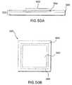
- FIG. 4illustrates a cross-sectional view of a die-up flex BGA package with heat spreader, according to an embodiment of the present invention.
- FIG. 5show a cross-sectional view of an alternative BGA package, according to embodiments of the present invention, where the heat spreader is internal to the BGA package.
- FIG. 6illustrates a cross-sectional view of a die-up flex BGA package with stiffener ground plane, according to an embodiment of the present invention.
- FIG. 9Billustrates a top view of the die-up tape BGA package with metal ring of FIG. 9A , according to an embodiment of the present invention.
- FIG. 10Aillustrates a stiffener that includes one or more thermal studs, according to an embodiment of the present invention.
- FIG. 10Billustrates an IC die that is wire bound to a substrate through openings in the stiffener of FIG. 10A , according to an embodiment of the present invention.
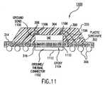
- FIG. 11illustrates a cross-sectional view of a die-up PBGA package with ground/thermal connector, according to an embodiment of the present invention.
- FIG. 12Aillustrates a cross-sectional view of a die-up BGA package.
- FIG. 14shows a flowchart related to FIGS. 4 and 5 , that provides operational steps of exemplary embodiments of the present invention.
- FIG. 15shows a flowchart related to FIG. 6 that provides operational steps of exemplary embodiments of the present invention.
- FIG. 17shows a flowchart related to FIGS. 9A and 9B that provides operational steps of exemplary embodiments of the present invention.
- FIG. 18shows a flowchart related to FIGS. 10A and 10B that provides operational steps of exemplary embodiments of the present invention.
- FIGS. 19A-Cshow flowcharts related to FIG. 11 that provide operational steps of exemplary embodiments of the present invention.
- FIG. 20illustrates a substrate that has a central window opening, according to an embodiment of the present invention.
- FIG. 21illustrates a side view of a stiffener that has a downward protruding portion, according to an embodiment of the present invention.
- FIG. 24shows first and second ground/thermal connectors attached to a bottom surface of a substrate, according to an exemplary embodiment of the present invention.
- FIG. 25shows first, second, third, and fourth ground/thermal connectors attached to a bottom surface of a substrate, according to an exemplary embodiment of the present invention.
- FIG. 27shows first and second ground/thermal connectors attached to a bottom surface of a substrate, according to an exemplary embodiment of the present invention.
- FIG. 28shows a bottom view of a corner portion of a substrate with potential via locations.
- FIGS. 29 and 30show an example bottom views of a corner portion of a substrate, according to embodiments of the present invention.
- FIG. 31shows a bottom view of an example BGA package, according to an embodiment of the present invention.
- FIG. 32shows a bottom view of the example BGA package of FIG. 31 , with electronic devices attached, according to an embodiment of the present invention.
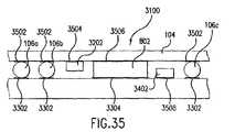
- FIG. 33shows a portion of a printed circuit board for mounting a BGA package, according to an exemplary embodiment of the present invention.
- FIG. 34shows the printed circuit board portion of FIG. 33 with electronic devices attached, according to an embodiment of the present invention.
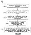
- FIGS. 36A and 36Bshow flowcharts providing operational steps for assembling embodiments of the present invention.
- FIG. 37Aillustrates a cross-sectional view of a die-up BGA package with ground/thermal connector and reduced-size stiffener, according to an embodiment of the present invention.
- FIGS. 37B-37Eillustrate views of exemplary BGA package stiffeners, according to embodiments of the present invention.
- FIG. 37Fillustrates a plan view of a substrate and stiffener, according to an embodiment of the present invention.
- FIGS. 38-40illustrate cross-sectional views of die-up BGA packages with ground/thermal connectors and reduced-size stiffeners, according to embodiments of the present invention.
- FIG. 41Aillustrates a cross-sectional view of a die-up BGA package with ground/thermal connector and full-size stiffener, according to an embodiment of the present invention.
- FIGS. 42-44illustrate cross-sectional views of die-up BGA packages with ground/thermal connectors and full-size stiffeners, according to embodiments of the present invention.
- FIG. 45illustrates a cross-sectional view of a die-up BGA package with ground/thermal connector that can extend into a PCB, according to an embodiment of the present invention.
- the present inventionis directed to a method and system for improving the mechanical, thermal, and electrical performance of BGA packages.
- the present inventionis applicable to all types of BGA substrates, including ceramic, plastic, and tape (flex) BGA packages. Furthermore the present invention is applicable to die-up (cavity-up) and die-down (cavity-down) orientations.
- BGA package thermal stress at the IC die/stiffener interfaceis released or altered with the introduction of a heat spreader on the top surface of the IC die, enabling large size dies with high input and output (I/O) counts to be packaged using BGA technology.
- BGA package thermal resistance and the length of the current return pathare reduced by introducing thermal/ground balls underneath or within close proximity of the IC die.
- the package thermal resistance and ground inductanceare reduced by removing center solder balls, and enabling the attachment of a die pad to the PCB.
- the die padis attached to the PCB with novel patternings of the metal stiffener, or by positioning a thermal/ground connector in between the IC die pad and the PCB.
- the package thermal resistanceis reduced by attaching a metal ring to the top surface of a stiffener.
- the package thermal resistanceis reduced by bridging the die pad to the outer regions of the stiffener with metal studs.
- the electrical performance of the BGA packageis improved.
- electrical performanceis improved by connecting ground bonds from the IC die to the stiffener.
- the stiffeneroperates as a package ground plane.
- the package ground planemay be connected to PCB ground through either thermal/ground balls or thermal/ground connectors mentioned in embodiments above, and further described herein.
- package power distributionis enhanced by using a layer in a tape substrate as a power or ground plane.
- plastic ball grid array (PBGA) package thermal and electrical performancesare improved.
- PBGAplastic ball grid array
- die-up and die-down BGA package configurationsexist.
- the IC dieis mounted on a top surface of the substrate or stiffener, in a direction away from the PCB.
- die-down BGA packagesthe IC die is mounted on a bottom surface of the substrate or stiffener, in a direction towards the PCB.
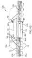
- FIG. 1Aillustrates a conventional flex BGA package 100 .
- Flex BGA package 100includes an IC die 102 , a tape substrate 104 , a plurality of solder balls 106 , and one or more wire bonds 108 .
- Tape or flex BGA packagesare particularly appropriate for large IC dies with large numbers of inputs and outputs, such as application specific integrated circuits (ASIC) and microprocessors.
- ASICapplication specific integrated circuits
- An encapsulate, mold compound, or epoxy 116covers IC die 102 and wire bonds 108 for mechanical and environmental protection.
- flex BGA package 100does not include a stiffener.
- a stiffenercan be attached to the substrate to add planarity and rigidity to the package.
- FIG. 1Billustrates a flex BGA package 110 , similar to flex BGA package 100 , that incorporates a stiffener 112 .
- Stiffener 112may be laminated to substrate 104 .
- Stiffener 112is typically made from a metal, or combination of metals, such as copper, tin, and aluminum, or may be made from a polymer, for example.
- Stiffener 112also may act as a heat sink, and allow for greater heat spreading in BGA package 110 .
- One or more openings 114 in stiffener 112may be used to allow for wire bonds 108 to connect IC die 102 to substrate 104 .
- Stiffener 112may be configured in other ways, and have different opening arrangements than shown in FIG. 1B .
- Plastic substrate 302includes one or more metal layers formed on an organic substrate.
- plastic or organic substratesmay include materials such as “BT”, which includes a resin called bis-maleimide triazine, and/or “FR-4,” which is a fire-retardant epoxy resin-glass cloth laminate material, and/or other similar materials.
- IC die 304is mounted to die pad 310 .
- IC die 304may be attached to die pad 310 with an epoxy, such as a silver-filled epoxy.
- Wire bonds 308connect signals of IC die 304 to substrate 302 . For instance, gold bonding wire is bonded from aluminum bond pads on IC die 304 to gold-plated contact pads on substrate 302 .
- the contact pads on substrate 302connect to solder balls 306 attached to the bottom surface of substrate 302 , through vias 314 and routing within substrate 302 using copper conductors 312 .
- Thermal/ground vias 316connect die pad 310 to one or more thermal/ground balls 322 on the center bottom surface of substrate 302 .
- An encapsulate, mold compound, or epoxy 320covers IC die 304 and wire bonds 308 for mechanical and environmental protection.
- wire bondssuch as wire bonds 1210
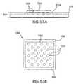
- IC diesmay be mounted and coupled to a substrate with solder balls located on the bottom surface of the IC die, by a process commonly referred to as “C4” or “flip chip” packaging.
- solder balls 1206may be arranged in an array.
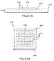
- FIG. 12Bshows a 14 by 14 array of solder balls on the bottom surface of BGA package 1200 .
- Other sized arrays of solder ballsare also applicable to the present invention.
- Solder balls 1206are reflowed to attach BGA package 1200 to a PCB.
- the PCBmay include contact pads to which solder balls 1206 are bonded.
- PCB contact padsare generally made from a metal or combination of metals, such as copper, nickel, tin, and gold.
- the solder ball arrangement shown in FIG. 12Cis particularly applicable to embodiments of the present invention described below, such as for attaching a heat spreader or ground/thermal connector to a bottom surface of a BGA package.
- the heat spreader or ground/thermal connectormay be connected in substrate center 1224 .
- the present inventionis applicable to improving thermal and electrical performance in the BGA package types described herein, and further BGA package types.
- a heat spreadermay be used in a BGA package to provide for thermal stress relief and heat dissipation.
- a drop-in heat spreaderis attached to the top surface of an IC die in a flex BGA package to provide for thermal stress relief and heat dissipation.
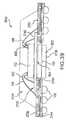
- FIG. 4illustrates a cross-sectional view of a die-up flex BGA package 400 , according to an embodiment of the present invention.
- BGA package 400includes IC die 102 , substrate 104 , plurality of solder balls 106 , one or more wire bonds 108 , stiffener 112 , epoxy 116 , a drop-in heat spreader 402 , and an adhesive 404 . Refer to the discussion above related to FIGS. 1A-1B for additional detail on the structure and operation of some of these elements.
- Substrate 104has a top surface to which a bottom surface of stiffener 112 is mounted. A bottom surface of substrate 104 attaches the plurality of solder balls 106 . The plurality of solder balls 106 connect to vias and/or points on the bottom surface of substrate 104 to which signals internal to substrate 104 are routed and exposed.
- Stiffener 112has a top surface to which IC die 102 is mounted.
- BGA package 400does not require a stiffener, and does not include a stiffener 112 .
- IC die 102is mounted to substrate 104 .
- wire bonds 108connect corresponding bond pads 118 on IC die 102 to contact points 120 on substrate 104 .
- wire bonds 108extend through one or more openings 114 in stiffener 112 to form connections with substrate 104 .
- Heat spreader 402is attached to the top surface (active surface) of IC die 102 using adhesive 404 .
- Adhesive 404may be an epoxy, an adhesive tape, or may be a different substance. Silver filled epoxies or thermally conductive tapes may be used for adhesive 404 to enhance heat extraction from IC die 102 .
- heat spreader 402is smaller in area than the upper surface of IC die 102 .
- Alternative sizes for heat spreader 402are also applicable to the present invention, including sizes equal to the area of IC die 102 , or larger areas.
- Heat spreader 402is shaped and configured to spread heat from IC die 102 , as is required by the application.
- FIG. 4the top surface of heat spreader 402 forms a portion of a top surface of BGA package 400 .
- Heat dissipation to the environmentcan be improved by exposing the top surface of heat spreader 402 .
- additional heat sinksmay be attached to heat spreader 402 .
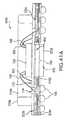
- FIG. 5show a cross-sectional view of an alternative BGA package 500 , according to embodiments of the present invention, where a heat spreader 502 is internal to BGA package 500 . Heat spreader 502 is completely encapsulated by epoxy 116 .
- the mechanical structure of BGA package 400becomes more symmetrical in its center region, particularly when ground/thermal solder balls do not exist on the bottom surface of substrate 104 underneath the outer profile of IC die 102 .
- Thermal stress at the interface of IC die 102 and stiffener 112is substantially released or altered by heat spreader 402 .
- Deformation caused by thermal stress in stiffener 112 and substrate 104is substantially reduced through the use of heat spreader 402 .
- Drop-in heat spreader 402allows for even larger sizes for IC die 102 and greater I/O counts by providing for greater heat spreading capacity in BGA package 400 .
- FIG. 14shows a flowchart 1400 providing operational steps for assembling one or more embodiments of the present invention.
- the steps of FIG. 14do not necessarily have to occur in the order shown, as will be apparent to persons skilled in the relevant art(s) based on the teachings herein.
- Other structural embodimentswill be apparent to persons skilled in the relevant art(s) based on the following discussion. These steps are described in detail below.
- Flowchart 1400begins with step 1402 .
- a substratethat has a first surface and a second surface is provided.
- the substrateis flex substrate 104 , or another substrate type suitable for a BGA package.
- an IC die mounting position and/or contact pointsare provided on a first, upper surface, and solder ball pads are provided on a second, bottom surface.
- a first surface of a stiffeneris attached to the first substrate surface.
- the stiffeneris stiffener 112 , which is attached to substrate 104 .
- a stiffeneris not required.
- an IC dieis mounted to the second stiffener surface.
- the IC dieis IC die 102 , which is mounted to stiffener 112 .
- IC die 102is mounted directly to the substrate.
- a heat spreaderis mounted to the IC die, wherein the heat spreader dissipates heat from the IC die.
- the heat spreaderis heat spreader 402 or 502 , which is mounted with adhesive 404 or other attachment means to the upper surface of IC die 102 .
- Heat spreader 402 or 502typically is mounted to the center of the upper surface of IC die 102 , and covers less than the entire upper surface of IC die 102 .
- the smaller area of heat spreader 402 or 502allows for bond pads 118 to be exposed on the upper surface of IC die 102 for wire bond connections.
- heat spreader 402 or 502is of the same size, or comprises a larger area than the upper surface of IC die 102 .
- a plurality of solder ballsare attached to the second substrate surface.
- the plurality of solder ballsare plurality of solder balls 106 , which connect to vias and/or solder ball pads on the bottom surface of substrate 104 .
- the solder ballsmay be arranged on the bottom surface of substrate 104 as shown in FIGS. 12B and 12C , or in alternative arrangements.
- the solder ballsare used to attach a BGA package to a PCB.
- a benefit of performing the steps of flowchart 1400is that the heat spreader relieves thermal stress at an interface of the IC die and the first stiffener surface.
- Flowchart 1400may include the additional step where the second stiffener surface is encapsulated.
- the second stiffener surfacemay be encapsulated by a resin or molding compound, that also encapsulates the IC die, heat spreader, and wire bonding.
- electrical performance of an IC die, and thermal performance of a corresponding BGA packagemay be improved by allowing a stiffener to act as a ground plane.
- a stiffener in a die-up tape BGA (Flex BGA) packageis coupled to PCB ground through one or more vias to ground solder balls.
- Ground contact pads of the IC dieare connected to the stiffener by ground wire bonds.
- one or more metal layers of a flex tape substratemay be coupled to a ground or power potential, to operate as a ground or power plane.
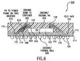
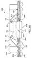
- FIG. 6illustrates a cross-sectional view of a die-up flex BGA package 600 , according to an embodiment of the present invention.
- BGA package 600includes IC die 102 , substrate 104 , plurality of solder balls 106 , one or more wire bonds 108 , stiffener 112 , epoxy 116 , one or more ground bonds to stiffener 602 , one or more ground/thermal vias 604 , one or more ground/thermal balls 606 , one or more ground contact pads 608 , one or more power contact pads 610 , and one or more power vias 612 .
- Stiffener 112has a top surface to which IC die 102 is mounted.
- Wire bonds 108connect corresponding bond pads 118 on IC die 102 to contact points 120 on substrate 104 .
- Wire bonds 108extend through one or more openings 114 in stiffener 112 to form connections with substrate 104 .
- IC die 102has a top surface that includes at least one ground pad 608 .
- Ground pad 608is coupled to a ground potential signal in IC die 102 .
- a ground wire bond 602connects ground pad 608 to stiffener 112 .
- the bottom surface of stiffener 112is coupled to a ground potential signal in the PCB to which BGA package 600 is attached, to cause stiffener 112 to operate as a ground plane.
- Stiffener 112is coupled to PCB ground through one or more of ground/thermal via 604 that extend through substrate 104 .
- the one or more of ground/thermal vias 604are located in substrate 104 , underneath IC die 102 , and can be filled with a conductive material, such as solder.
- a tape substrateis configured such that a metal layer is used as a package power or ground plane.
- a metal layeris used as a package power or ground plane.
- the bottom metal layermay be used as a power or ground plane.
- PCB package 600includes a bottom metal layer 614 of a two-layer tape substrate 104 that is coupled to a potential to operate as a power plane, according to an embodiment of the present invention.
- One or more power contact pads 610 on IC die 102are coupled to a power potential signal in IC die 102 .
- Power contact pad 610 on IC die 102is connected to a corresponding power via 612 by a power wire bond 616 .
- power wire bond 616extends through opening 114 .
- Power via 612extends through substrate 104 .
- Power via 612can be filled with a conductive material, such as solder.
- Each power via 612is coupled to the bottom metal layer 614 of substrate 104 .
- one or more power vias 612may be connected to corresponding solder balls on the bottom of substrate 104 , to connect bottom metal layer 614 to PCB power pads when the solder balls are reflowed.
- a stiffener ground plane, and/or a power/ground plane using a metal layer of a tape substrateallows for very short power and ground connections.
- Current return path lengthsare shortened, voltage drop across planes is reduced, and power/ground inductance is reduced.
- the shorter power and ground pathsare also significant in reducing a power/ground path resistance, which advantageously reduces required IC device power levels.
- thermal vias in a flex tape substrateand of the use of a thermal ball coupled to a heat spreader in a die-down TBGA package, refer to U.S. Pat. No. 6,020,637, which is incorporated by reference in its entirety herein.
- thermal via and a thermal ball in a plastic substrate BGA packagerefer to U.S. Pat. No. 5,894,410, which is incorporated by reference in its entirety.
- FIG. 15shows a flowchart 1500 providing operational steps for assembling one or more embodiments of the present invention.
- the steps of FIG. 15do not necessarily have to occur in the order shown, as will be apparent to persons skilled in the relevant art(s) based on the teachings herein.
- Other structural embodimentswill be apparent to persons skilled in the relevant art(s) based on the following discussion. These steps are described in detail below.
- Flowchart 1500begins with step 1502 .
- a substratethat has a first surface and a second surface is provided.
- the substrateis flex substrate 104 , or another substrate type suitable for a BGA package.
- an IC die mounting position and/or contact pointsare provided on a first, upper surface, and solder ball pads are provided on a second, bottom surface.
- step 1504at least one opening in a stiffener from a first surface of the stiffener to a second surface of the stiffener is provided.
- the at least one openingincludes openings 114 in stiffener 112 .
- an opening 114is located on each of the four edges of IC die 102 .
- the first stiffener surfaceis attached to the first substrate surface.
- the stiffeneris stiffener 112 , which is attached to substrate 104 .
- a stiffeneris not required, and is not attached to the substrate.
- an integrated circuit (IC) dieis mounted to the second stiffener surface, wherein a first surface of the IC die includes a contact pad.
- the IC dieis IC die 102 , which is mounted to stiffener 112 .
- IC die 102is mounted directly to the substrate.
- the contact padis ground contact pad 608 .
- the contact padis coupled to the second stiffener surface.
- contact padis ground contact pad 608 , which is connected to stiffener 112 by ground wire bond 602 .
- Ground wire bond 602may be soldered, or otherwise attached to stiffener 112 .
- a plurality of solder ballsis attached to the second substrate surface, inside an outer dimensional profile of the IC die.
- the plurality of solder ballsinclude one or more ground/thermal balls 606 , which are arranged on the bottom surface of substrate 104 in the region of substrate center 1224 , shown in FIG. 12C .
- the outer dimensional profile of the IC dieis the area bounded by the edges of IC die 102 .
- the plurality of solder ballsare coupled through corresponding vias in the substrate to the first stiffener surface.
- the viasinclude ground/thermal via 604 .
- the viascan be filled with a conductive material, such as solder, to allow the electrical connection of the solder balls to stiffener 112 .
- the substrateincludes a metal layer, wherein the metal layer is coupled to a second potential.
- the stiffenerhas at least one opening extending from the first stiffener surface to the second stiffener surface.
- the second IC die surfaceincludes a second contact pad.
- the second contact padis coupled to the metal layer through one of the openings in the stiffener and through a corresponding via that extends through the substrate.
- the second contact padmay be coupled to a power or ground potential in the IC die.
- the second contact padis power contact pad 610
- the metal layeris metal layer 614
- the corresponding viais power via 612 .
- flowchart 1500may include an additional step, where the contact pad is coupled to a ground potential in the IC die.
- the contact padmay be connected to a ground plane or ground signal in IC die that is routed to the contact pad.
- Flowchart 1500may include the additional step where the second stiffener surface is encapsulated.
- the second stiffener surfacemay be encapsulated by a resin or molding compound, that also encapsulates the IC die and wire bonding.
- Flowchart 1500may include the additional step where a second plurality of solder balls is attached to the second substrate surface, outside an outer dimensional profile of the IC die.
- the second plurality of solder ballsare plurality of solder balls 106 , which connect to vias and/or solder ball pads on the bottom surface of substrate 104 .
- the solder ballsare arranged on the bottom surface of substrate 104 as shown in FIG. 12B , outside of substrate center 1224 .
- the solder ballsare used to attach a BGA package to a PCB.
- electrical performance of the IC device, and thermal performance of a BGA packageis improved by enabling an IC die pad to attach to a PCB.
- the IC die padis attached to the PCB by a novel patterning of the metal stiffener in a die-up tape BGA package.
- the IC die padis attached to the PCB by placing a thermal/ground connector between the IC die pad and PCB in a die-up tape BGA package.
- a BGA package junction-to-board thermal resistancecan be substantially reduced by the attachment of a metal die-attach pad directly to a PCB.
- Metal die-attach padsare coupled to a PCB for package junction-to-board thermal resistance minimization in an exposed pad quad flat pack (QFP), a QFP with exposed heat sink at bottom, and a leadless plastic chip carrier (i.e. LPCC, QFN, SON, QLP) package, for instance.
- QFPexposed pad quad flat pack
- QFPQFP with exposed heat sink at bottom
- a leadless plastic chip carrieri.e. LPCC, QFN, SON, QLP
- All existing such designs that involve an exposed die pad or an exposed heat sink at package bottomare “lead frame” packages.
- the present inventionprovides for an exposed die-attach pad or heat sink at the bottom of flex BGA packages.
- FIG. 7illustrates a cross-sectional view of a die-up flex BGA package 700 , according to an embodiment of the present invention.
- BGA package 700includes IC die 102 , substrate 104 , plurality of solder balls 106 , one or more wire bonds 108 , stiffener 112 , epoxy 116 , ground wire bond to stiffener 602 , ground contact pad 608 , and a stiffener cavity 702 .
- Substrate 104has a top surface to which a bottom surface of stiffener 112 is mounted. A bottom surface of substrate 104 attaches the plurality of solder balls 106 . The plurality of solder balls 106 connect to vias and/or points on the bottom surface of substrate 104 to which signals internal to substrate 104 are routed and exposed. Substrate 104 in FIG. 7 has a central window-shaped opening 704 , under which solder balls are preferably not connected.
- FIG. 20illustrates a bottom view of a substrate 104 that has a central window opening 704 , according to an embodiment of the present invention.
- Stiffener 112has a top surface to which IC die 102 is mounted. Stiffener 112 in FIG. 7 is patterned with a cavity 702 , which protrudes downward for attachment of IC die 102 . As described above, a central window-shaped opening 704 exists in substrate 104 . This opening 704 exists to allow stiffener 112 to protrude through, and make contact with soldering pads on a PCB to which BGA package 700 is to be mounted. The bottom exposed surface of cavity 702 can be plated with solder to facilitate surface mount to solder plated metal pads on a PCB to which BGA package 700 is mounted. Hence, stiffener 112 may act as a conduit for heat to be transferred from IC die 102 to the PCB.
- Stiffener 112may optionally be configured to operate as a ground plane.
- One or more ground pads 608may be coupled to a ground potential signal in IC die 102 .
- a ground wire bond 602connects each ground pad 608 to stiffener 112 .
- the bottom exposed surface of cavity 702may function both as an exposed ground pad of BGA package 700 , and as an exposed heat spreader.
- the bottom exposed surface of cavity 702may be plated with solder to allows stiffener 112 to be surface mounted to one or more soldering pads on the PCB.
- the pads on the PCBcan be connected to a PCB ground plane to shorten the length of electrical current return paths, as well as to form a conductive heat dissipation path from BGA package 700 to the PCB.
- FIG. 8illustrates a cross-sectional view of a die-up flex BGA package 700 , according to an embodiment of the present invention.
- Substrate 104 in FIG. 8has a central window-shaped opening, under which no solder balls are connected.
- a portion of the bottom surface of stiffener 112is exposed through the central window-shaped opening 704 of substrate 104 .
- a heat spreader(for example, manufactured from copper or aluminum), shown as ground/thermal connector 802 , is coupled to the exposed portion of stiffener 112 .
- Ground/thermal connector 802can be made from the same material as stiffener 112 .
- Ground/thermal connector 802may be laminated to the exposed portion of stiffener 112 using conductive epoxy or solder.
- the bottom surface of ground/thermal connector 802may be plated with solder to facilitate its surface mount to soldering pads on the PCB.
- Metal pads on the PCBmay be connected to a PCB ground plane to shorten the length of electrical current return paths, as well as enhance the conductive heat dissipation path from IC die 102 to the PCB.
- stiffener 112 and ground/thermal connector 802may be manufactured from a single piece of metal, and hence consist of a single metal piece.
- FIG. 21illustrates a side view of stiffener 112 that has a downward protruding portion 2102 , according to an embodiment of the present invention.
- portion 2102extends partially or entirely through window-shaped opening 704 .
- Portion 2102may be directly connected to the PCB, or may be connected to a ground/thermal connector 802 that is connected to the PCB. Because of the thermal and electrical improvement enabled by the coupling of stiffener 112 to a PCB, length of wire bonds can be reduced by moving opening 114 closer to the proximity of die 102 without compromising thermal performance significantly.
- FIG. 16Ashows a flowchart 1600 providing operational steps for assembling one or more embodiments of the present invention.
- FIGS. 16B-Dprovide operational steps according to further embodiments. The steps of FIGS. 16A-D do not necessarily have to occur in the order shown, as will be apparent to persons skilled in the relevant art(s) based on the teachings herein. Other structural embodiments will be apparent to persons skilled in the relevant art(s) based on the following discussion. These steps are described in detail below.
- Flowchart 1600begins with step 1602 .
- a substratethat has a first surface and a second surface is provided.
- the substrateis flex substrate 104 , or another substrate type suitable for a BGA package.
- an IC die mounting position and/or contact pointsare provided on a first, upper surface, and solder ball pads are provided on a second, bottom surface.
- a first surface of a stiffeneris attached to the first substrate surface.
- the stiffeneris stiffener 112 , which is attached to substrate 104 .
- step 1606a portion of the first stiffener surface is exposed through a window opening in the substrate.
- substrate 104has a window opening 704 in its center. A portion of the bottom surface of stiffener 112 is exposed through window opening 704 .
- an IC dieis mounted to a second surface of the stiffener, wherein a surface of the IC die includes at least one contact pad.
- the IC dieis IC die 102 , which is mounted to stiffener 112 .
- a plurality of solder ballsare attached to the second substrate surface.
- the plurality of solder ballsare plurality of solder balls 106 , which connect to vias and/or solder ball pads on the bottom surface of substrate 104 .
- the solder ballsare arranged on the bottom surface of substrate 104 as shown in FIG. 12B , exclusive of the area of window opening 704 .
- the solder ballsare used to attach a BGA package to a PCB.
- the exposed portion of the first stiffener surfaceis configured to be coupled to a printed circuit board (PCB), whereby electrical and thermal performance of the BGA package is improved.
- PCBprinted circuit board
- FIG. 16Bprovides exemplary steps for performing step 1612 :
- a heat spreaderis coupled to the exposed portion of the first stiffener surface.
- the heat spreaderis ground/thermal connector 802 , which is coupled to stiffener 112 through window opening 702 .
- step 1616a surface of the heat spreader is configured to be coupled to the PCB.
- step 1612further includes the step where the heat spreader surface is plated with solder to allow the heat spreader surface to be surface mounted to soldering pads on the PCB.
- step 1612comprises the step where the stiffener is shaped to have a centrally-located cavity shaped portion that protrudes through the window opening.
- step 1612further includes the step where a surface of the cavity shaped portion is plated with solder to allow the stiffener to be surface mounted to soldering pads on the PCB.
- stiffener 112is patterned with a cavity 702 , which protrudes downward in window opening 704 .
- the bottom surface of cavity 702is plated with solder.
- FIG. 16Cprovides additional exemplary steps for flowchart 1600 of FIG. 16A :
- the stiffeneris coupled to a potential.
- the stiffenermay be coupled to ground or power on the PCB.
- the bottom surface of cavity 702may be coupled to the ground or power potential on the PCB, or ground/thermal connector 802 may make the connection to the PCB.
- each of the at least one contact padsare coupled to the second stiffener surface with corresponding wire bonds.
- FIG. 16Dprovides exemplary steps for performing step 1618 :
- step 1622the stiffener is coupled to a ground potential.
- step 1624the stiffener allowed to serve as a ground plane.
- Flowchart 1600may include the additional step where the second stiffener surface is encapsulated.
- the second stiffener surfacemay be encapsulated by an epoxy, that also encapsulates the IC die and wire bonding.
- the mechanical and thermal performance of a BGA packageis enhanced by attaching a metal ring to the top surface of the stiffener.
- a metal ringis attached to the top surface of the stiffener in a die-up tape BGA package.
- FIG. 9Aillustrates a cross-sectional view of a die-up tape BGA package 900 , according to an embodiment of the present invention.
- BGA package 900includes IC die 102 , substrate 104 , plurality of solder balls 106 , one or more wire bonds 108 , stiffener 112 , epoxy 116 , and a ring 902 .
- FIG. 9Billustrates a top view of die-up tape BGA package 900 , with ring 902 .
- Substrate 104has a top surface to which a bottom surface of stiffener 112 is mounted. A bottom surface of substrate 104 attaches the plurality of solder balls 106 . The plurality of solder balls 106 connect to vias and/or points on the bottom surface of substrate 104 to which signals internal to substrate 104 are routed and exposed.
- One or more wire bonds 108connect corresponding bond pads 118 on IC die 102 to contact points 120 on substrate 104 .
- Wire bonds 108extend through one or more openings 114 in stiffener 112 to form connections with substrate 104 .
- Stiffener 112has a top surface to which IC die 102 is mounted.
- ring 902is attached to the top surface of stiffener 112 .
- Ring 902may be laminated to stiffener 112 , after wire bonding is completed.
- Epoxy 116is filled in and flushed to ring 902 after the attachment of ring 902 .
- Ring 902is preferably made of a metal, such as copper or aluminum, or a combination thereof, but may be constructed from other applicable materials.
- ring 902is made from the same material as stiffener 112 , to minimize the mismatch of the thermal expansion coefficient. Ring 902 is preferably flush with the outer edges of stiffener 112 to form an outer edge of BGA package 900 , but may also reside entirely within an outer profile of stiffener 112 .
- a primary benefit of attaching ring 902 to stiffener 112is an increase in stiffness of BGA package 900 .
- Ring 902also aids in reducing the amount of warp of BGA package 900 .
- ring 902promotes heat dissipation from stiffener 112 , reduces junction-to-case thermal resistance, and facilitates the attachment of an external heat spreader to BGA package 900 .
- Ring 902enhances the process of encapsulation of the BGA package.
- Ring 902with stiffener 112 , creates a cavity that may be filled with a dispensed glob top or encapsulating material, that locks IC die 102 and surrounding elements in place.
- FIG. 17shows a flowchart 1700 providing operational steps for assembling one or more embodiments of the present invention.
- the steps of FIG. 17do not necessarily have to occur in the order shown, as will be apparent to persons skilled in the relevant art(s) based on the teachings herein.
- Other structural embodimentswill be apparent to persons skilled in the relevant art(s) based on the following discussion. These steps are described in detail below.
- Flowchart 1700begins with step 1702 .
- a substratethat has a first surface and a second surface is provided.
- the substrateis flex substrate 104 , or another substrate type suitable for a BGA package.
- an IC die mounting position and/or contact pointsare provided on a first, upper surface, and solder ball pads are provided on a second, bottom surface.
- a first surface of a stiffeneris attached to the first substrate surface.
- the stiffeneris stiffener 112 , which is attached to substrate 104 .
- a stiffeneris not required, and is not attached to the substrate.
- an IC dieis mounted to the first stiffener surface.
- the IC dieis IC die 102 , which is mounted to stiffener 112 .
- IC die 102is mounted directly to the substrate.
- a plurality of solder ballsare attached to the second substrate surface.
- the plurality of solder ballsare plurality of solder balls 106 , which connect to vias and/or solder ball pads on the bottom surface of substrate 104 .
- the solder ballsmay be arranged on the bottom surface of substrate 104 as shown in FIGS. 12B and 12C , or in alternative arrangements.
- the solder ballsare used to attach a BGA package to a PCB.
- a metal ringis attached to the first stiffener surface. Attaching the metal ring enhances heat dissipation from the stiffener.
- the metal ringis ring 902 .
- ring 902is attached directly to the substrate.
- Flowchart 1700may include the additional step where the second stiffener surface within the volume encompassed by the ring is encapsulated.
- a filled upper surfacemay be called a “glob top”.
- this volumemay be encapsulated by a resin or molding compound, that also encapsulates the IC die and wire bonding.
- the thermal performance of a BGA packageis improved by bridging an IC die pad to which the IC die is mounted to the outer regions of the stiffener.
- one or more metal studsare used as thermal bridges, to bridge the openings in the stiffener that surround the IC die, in a die-up tape BGA package.
- the openings on a stiffener surfaceallow for wire bond connections between an IC die and a substrate. These openings have the additional effect of reducing the amount of heat that can spread to the outer surface regions of the stiffener, hampering the ability of the stiffener to act as a heat spreader. This effect is illustrated in FIG. 2B , which is further described above.
- the stiffeneris patterned such that one or more short studs run across each wire bond opening. More than one stud may be used to bridge each wire bond opening to promote heat spreading.
- the manufacturing process used for lead frame patterningmay be adapted to pattern a stiffener with studs across the wire bond openings. The use of the studs, however, may reduce space for wire bonds, and may reduce BGA package I/O capability, in some situations.
- FIG. 10Aillustrates a stiffener 1000 , that includes one or more studs 1002 , according to an embodiment of the present invention.
- Stiffener 1000having one or more studs 1002 , may be incorporated into a BGA package in the same manner as is described elsewhere herein for stiffener 112 .
- a stud 1002bridges each opening 114 in stiffener 1000 .
- more than one stud 1002 per opening 114may be used.
- each opening 114may be bridged by a different number of studs 1002 . Some of openings 114 may be bridged by one or more studs 1002 , while other openings 114 may not be bridged at all.
- FIG. 10Bprovides an illustration where IC die 102 is wire bound to substrate 104 through stiffener 1000 , according to an embodiment of the present invention.
- One or more wire bonds 108connect corresponding bond pads 118 on IC die 102 to contact points 120 on substrate 104 .
- Wire bonds 108avoid studs 1002 when making connections to substrate 104 .
- FIG. 18shows a flowchart 1800 providing operational steps for assembling one or more embodiments of the present invention.
- the steps of FIG. 18do not necessarily have to occur in the order shown, as will be apparent to persons skilled in the relevant art(s) based on the teachings herein.
- Other structural embodimentswill be apparent to persons skilled in the relevant art(s) based on the following discussion. These steps are described in detail below.
- Flowchart 1800begins with step 1802 .
- a substratethat has a first surface and a second surface is provided.
- the substrateis flex substrate 104 , or another substrate type suitable for a BGA package.
- an IC die mounting position and/or contact pointsare provided on a first, upper surface, and solder ball pads are provided on a second, bottom surface.
- a wire bond openingis created along each edge of an IC die mount position on a stiffener, wherein each wire bond opening extends through the stiffener.
- the wire bond openingsare wire bond openings 114 in stiffener 1000 .
- the IC die mount positionis IC die mounting position 202 , shown in FIG. 10A .
- an IC dieis mounted to a second surface of the stiffener.
- the IC dieis IC die 102 , which is mounted to stiffener 1000 , in IC die mounting position 202 .
- step 1810at least one of the wire bond openings are bridged with at least one stud.
- one or more of wire bond openings 114are bridged with one or more studs 1002 . Studs 1002 allow for increased heat spreading across corresponding wire bond openings 114 to the outer edges of stiffener 1000 .
- a plurality of solder ballsare attached to the second substrate surface.
- the plurality of solder ballsare plurality of solder balls 106 , which connect to vias and/or solder ball pads on the bottom surface of substrate 104 .
- the solder ballsmay be arranged on the bottom surface of substrate 104 as shown in FIGS. 12B and 12C , or in alternative arrangements.
- the solder ballsare used to attach a BGA package to a PCB.
- the flowchart 1800may include the further step where a contact pad on the IC die is coupled to the substrate with a wire bond, wherein the wire bond passes through one of the wire bond openings in the stiffener.
- Flowchart 1800may include the additional step where the second stiffener surface is encapsulated.
- the second stiffener surfacemay be encapsulated by a resin or molding compound, that also encapsulates the IC die and wire bonding.
- the electrical and thermal performance of a plastic BGA (PBGA) packageis improved by attaching a thermal/ground connector to the bottom surface of a PBGA package.
- the thermal/ground connectorcouples the bottom center of a plastic substrate of a die-up PBGA to the PCB. Heat from an IC die is more easily spread to the PCB through the thermal/ground connector, which is attached to the plastic substrate underneath the IC die.
- FIG. 8embodiments were described that used a ground/thermal connector to couple a flex BGA package to a PCB, to reduce package junction-to-board thermal resistance. Aspects of this discussion above are adaptable to other die-up BGA package types. These include BGA packages having an organic substrate, such as PBGA and fine pitch ball grid array (FBGA) packages. Further detailed description is provided in the following discussion that is applicable to BGA packages with organic substrates.
- BGA packages having an organic substratesuch as PBGA and fine pitch ball grid array (FBGA) packages.
- FIG. 11illustrates a cross-sectional view of a die-up PBGA package 1100 , according to an embodiment of the present invention.
- PBGA package 1100includes plastic substrate 302 , IC die 304 , plurality of solder balls 306 , plurality of wire bonds 308 , die pad 310 , one or more vias 314 , one or more thermal/ground vias 316 , epoxy 320 , a ground/thermal connector 1102 , adhesive material 1104 , a plurality of ground bonds 1106 , and a plurality of ground bond pads 1108 .
- IC die 304is mounted to die pad 310 .
- Wire bonds 308connect signals of IC die 304 to contact pads on substrate 302 .
- the contact pads on substrate 302connect to solder balls 306 attached to the bottom surface of substrate 302 , through vias 314 and routing within substrate 302 .
- Thermal/ground vias 316connect die pad 310 to an exposed metal plane 1110 at the bottom center of substrate 302 .
- die pad 310 and metal plane 1110may be exposed copper pads of plastic substrate 302 .
- BGA package 1100provides a thermal path of IC die 304 , to die pad 310 , to thermal/ground vias 316 , to metal plane 1110 , to adhesive material 1104 , to ground thermal connector 1102 (and bottom surface 1112 ) to the PCB soldering pads. Heat spreading is improved by a direct thermal path from IC die 304 to the PCB.
- Metal pads on the PCBcan be connected to a PCB ground plane to advantageously shorten the length of electrical current return paths, as well shorten the conductive heat dissipation path from device junctions of IC die to the PCB.
- Ground bonds 1106may be used to couple ground bond pads 1108 on IC die 304 to die pad 310 , when die pad 310 is coupled to ground. This provides for very short ground connections for signals in IC die 304 .
- Flowchart 1900begins with step 1902 .
- a substratethat has a first surface and a second surface is provided.
- the substrateis plastic substrate 302 , or another substrate type suitable for a BGA package.
- an IC die mounting position and contact pointsare provided on a first, upper surface, and solder ball pads are provided on a second, bottom surface.
- a plurality of solder ballsare attached to the second substrate surface.
- the plurality of solder ballsare plurality of solder balls 306 , which connect to vias and/or solder ball pads on the bottom surface of substrate 302 .
- the solder ballsmay be arranged on the bottom surface of substrate 302 as shown in FIG. 12B , or in other arrangements.
- the solder ballsare used to attach a BGA package to a PCB.
- a first surface of a heat spreaderis coupled to the second substrate surface.
- the heat spreaderis ground/thermal connector 1102 , which is coupled to substrate 302 with adhesive material 1104 .
- Ground/thermal connector 1102may be mounted to metal plane 1110 on substrate 302 by adhesive material 1104 .
- a second surface of the heat spreaderis configured to be coupled to a printed circuit board (PCB).
- Second heat spreader surfaceis bottom surface 1112 .
- step 1910may include the step where the second surface of the heat spreader is plated with solder.
- FIG. 19Bprovides exemplary steps for performing step 1904 :
- the IC dieis mounted to the copper plated die-attach pad.
- the IC diemay be mounted with an epoxy.
- FIG. 19Cprovides exemplary steps for performing step 1908 :
- step 1918the die-attach pad is coupled to the copper plated plane with at least one via.
- Flowchart 1900may include the additional step where the first substrate surface is encapsulated.
- the first substrate surfacemay be encapsulated by a resin or molding compound, that also encapsulates the IC die and wire bonding.
- FIG. 22illustrates a cross-sectional view of a portion of die-up PBGA package 1100 , according to an embodiment of the present invention.
- PBGA package 1100includes plastic substrate 302 , IC die 304 , plurality of solder balls 306 , one of the plurality of wire bonds 308 , epoxy 320 , ground/thermal connector 1102 , adhesive material 1104 , metal plane 1110 , a connector plating 2202 , and plurality of solder ball contact pads 2224 (vias 314 and 316 , ground bonds 1106 , and pads 310 and 1108 are not shown in FIG. 22 ).
- PBGA package 1100is substantially configured as described above, and as further described below. Also shown in FIG. 22 is a cross-sectional view of a portion of an exemplary printed circuit board (PCB) 2222 , according to an embodiment of the present invention.
- PCB 2222includes a PCB substrate 2212 , a PCB metal pad plating 2214 , a PCB metal pad 2216 , and plurality of solder ball contact pads 2226 .
- PCB 2222includes a PCB substrate 2212 , a PCB metal pad plating 2214 , a PCB metal pad 2216 , and plurality of solder ball contact pads 2226 .
- PBGA package 1100is attached to PCB 2222 in order for IC die 304 to be interfaced with an electronic circuit system.
- IC die 304is mounted to substrate 302 .
- Wire bond 308connects one or more signals of IC die 304 to contact pads (not shown) on the top surface of substrate 302 . These contact pads connect through substrate 302 to solder ball contact pads 2224 exposed through the solder mask on the bottom surface of substrate 302 . Solder balls 306 attach to solder ball contact pads 2224 .
- Ground/thermal connector 1102is attached to metal plane 1110 .
- Metal plane 1110is a portion of a metal layer of substrate 302 exposed though the solder mask on the bottom surface of substrate 302 .
- ground/thermal connector 1102may be a metal piece or slug (copper or aluminum, for example) similar to the heat spreaders described elsewhere herein, that is laminated to metal plane 1110 at the bottom center of substrate 302 using a conductive adhesive material 1104 , such as a conductive epoxy, solder, or other adhesive material.
- a bottom surface 1112 of ground/thermal connector 1102may be plated with a metal (including a metal alloy), such as a solder, which may include palladium, nickel, tin, gold, silver, lead and/or further related substance(s), to form connector plating 2202 .
- a metalincluding a metal alloy
- solderwhich may include palladium, nickel, tin, gold, silver, lead and/or further related substance(s)
- Connector plating 2202enhances the surface mounting of connector 1102 to PCB 2222 .
- the top surface of PCB substrate 2212includes solder ball contact pads 2226 for surface mount of solder balls 306 to PCB 2222 , and includes PCB metal pad 2216 for surface mount of connector 1102 to PCB 2222 .
- PCB metal pad plating 2214may be attached to PCB metal pad 2216 to enhance the surface mounting of connector 1102 to PCB metal pad 2216 .
- PCB metal pad 2216may be screen printed with a solder paste to form PCB metal pad plating 2214 .
- PCB metal pad plating 2214also may be formed in other known manners from processes and substances described herein or elsewhere.
- Heat spreadingis improved in package 1100 by a direct thermal path from IC die 304 through connector 1102 to PCB 2222 .
- PCB metal pad 2216 on PCB 2222can be connected to a PCB ground plane to advantageously shorten the length of electrical current return paths, as well shorten the conductive heat dissipation path from device junctions of IC die 304 to PCB 2222 .
- viasmay be created in substrate 302 , and filled with a conductive material, to enhance thermal and electrical performance by coupling IC die 304 to connector 1102 more directly.
- Example implementations for package 1100 and PCB 2222 according to the present inventionwill now be described. These implementations are provided for purposes of illustration, and are not intended to limit the scope of the invention. Alternate implementations, differing slightly or substantially from those described herein, will be apparent to persons skilled in the relevant art(s) based on the teachings contained herein. Such alternate implementations fall within the scope and spirit of the present invention.
- FIG. 22illustrates various dimensions of package 1100 and PCB 2222 .
- package 1100the following dimensions are shown: an adhesive material height 2204 , a connector height 2206 , a connector plating height 2208 , a solder ball height 2218 , and a ball pitch 2220 .
- PCB 2222a PCB metal pad plating height 2210 is shown. These dimensions of package 1100 and PCB 2222 may have a variety of values, according to the present invention.
- ground/thermal connector 1102may be attached to metal plane 1110 on substrate 302 by adhesive material 1104 that has an adhesive material height 2204 in the range of 1 to 1.5 mil (0.025 to 0.0375 mm).
- Connector 1102has a connector height 2206 equal to 0.38 mm.
- Connector plating 2202has a connector plating height 2208 equal to 1 mil (0.025 mm). According to these example height values, the sum of adhesive material height 2204 (using a value of 0.025 mm), connector height 2206 , and connector plating height 2208 is 0.43 mm.
- solder balls 306may have a height of 0.6 mm, for example.
- Ball pitch 2220which represents the distance from the center of a solder ball mounted to substrate 302 to the center of an adjacent solder ball, is equal to 1 mm, for example.
- the height of solder balls 306may decrease slightly, to have a solder ball height 2218 equal to 0.5 mm, for example. This decrease in height is due to the spreading of solder of the solder ball onto a solder ball pad 2224 to which it is attaching.
- the difference in height between the solder ball height 2218 (0.5 mm) and the sum of adhesive material height 2204 , connector height 2206 , and connector plating height 2208 (0.43 mm)is equal to 0.07 mm, which is the value of a gap distance.
- this gap distanceappears between connector plating 2202 and PCB 2222 .
- the gap distancemay vary between 2.0 to 4.0 mils (0.05 to 0.1 mm), or even outside of this range, due to variations in the actual height values recited above that occur during the manufacturing process.
- solder ball height 2218is greater than the height of the attached connector 1102 (including connector height 2206 , adhesive material height 2204 , and connector plating height 2208 , when present), although in alternative embodiments, the attached connector 1102 may have an equal height.
- PCB metal pad plating 2210may be formed on PCB metal pad 2216 .
- PCB metal pad plating 2210substantially bridges the above described gap distance, and enhances the connection of connector 1102 to PCB 2222 .
- PCB metal pad plating 2214may be formed such that PCB metal pad plating height 2210 is in the range of 4 to 6 mil (0.1 to 0.15 mm) to substantially fill the gap distance.
- ball pitch 2220may be equal to 1.27 mm and solder ball height 2218 may be equal to 0.75 or 0.76 mm.
- these dimensionsmay have other values. As described above, the dimension values provided in the section are examples, and are not limiting to the present invention.
- ground/thermal connector 1102may be shaped in additional ways, to enhance the operation and manufacturability of package 1100 .
- FIG. 23shows ground/thermal connector 1102 attached to a bottom surface of substrate 302 , according to an exemplary embodiment of the present invention.
- Connector 1102is attached to metal plane 1110 , and is plated with connector plating 2202 .
- connector 1102may be rectangular in shape.
- Ground/thermal connector 1102may be formed in other shapes, such as an ellipse, polygon, star-shaped, and irregular.
- connector 1102is smaller in area than metal plane 1110 .
- connector 1102may have the same area, or a greater area than metal plane 1110 .
- Ground/thermal connector 1102may also include two or more separate sub-sections that are attached to package 1100 .
- FIG. 24shows first and second ground/thermal connectors 2402 and 2404 attached to a bottom surface of substrate 302 , according to an exemplary embodiment of the present invention. Connector plating, which may be present on first and second ground/thermal connectors 2402 and 2404 , is not shown in FIG. 24 .
- First ground/thermal connector 2402is attached to first metal plane 2406 on substrate 302 .
- Second ground/thermal connector 2404is attached to second metal plane 2408 on substrate 302 .
- first and second metal planes 2406 and 2408may be combined into a single metal plane, or may be each divided into any number of metal planes, for attachment of first and second ground/thermal connectors 2402 and 2404 to substrate 302 .
- one or more PCB metal padsmay be present on PCB substrate 2212 (shown in FIG. 22 ) to attach first and second ground/thermal connectors 2402 and 2404 to PCB 2222 .
- ground/thermal connectormay enhance the functionality, thermal performance, electrical performance, mechanical performance, and the manufacturability of package 1100 .
- electrical performancemay be enhanced by electrically isolating first and second connectors 2402 and 2404 , and coupling them to separate potentials (i.e., ground or other potentials) of IC die 304 (through vias in substrate 302 ).
- First and second connectors 2402 and 2404may then be coupled to the separate potential signals in PCB 2222 .
- FIG. 25shows first, second, third, and fourth ground/thermal connectors 2502 , 2504 , 2506 , and 2508 attached to a bottom surface of substrate 302 , according to a further exemplary embodiment of the present invention.
- Connector platingwhich may be present on first, second, third, and fourth ground/thermal connectors 2502 , 2504 , 2506 , and 2508 , is not shown in FIG. 25 .
- First, second, third, and fourth ground/thermal connectors 2502 , 2504 , 2506 , and 2508are attached to first, second, third, and fourth metal planes 2510 , 2512 , 2514 , and 2516 , respectively, on substrate 302 .
- ground/thermal connectorsmay be shaped and arranged in a variety of configurations.
- one or more ground/thermal connectorsmay be formed around a portion of, or all of one or more other ground/thermal connectors.
- FIG. 27shows first and second ground/thermal connectors 2702 and 2704 attached to a bottom surface of substrate 302 , according to a further exemplary embodiment of the present invention.
- First and second ground/thermal connectors 2702 and 2704are attached to first and second metal planes 2706 and 2708 . As shown in FIG.
- first ground/thermal connector 2702is formed in a substantially rectangular shape
- second ground/thermal connector 2704is formed in a substantially rectangular ring shape that surrounds first ground/thermal connector 2702 on the bottom surface of substrate 302 .
- First metal plane 2706is correspondingly formed in a rectangular-shaped metal plane
- second metal plane 2708is formed in a rectangular ring-shaped metal plane. As shown in FIG. 27 , a portion of the bottom surface of substrate 302 is present between first and second metal planes 2706 and 2708 .
- FIG. 28shows a bottom view of a corner portion of substrate 302 with potential via locations.
- Substrate 302 of FIG. 28is divided into a peripheral region 2804 and a central region 2806 .
- the central region 2806corresponds to the portion of the substrate adjacent to a mounted IC die 102 (and corresponding metal pad) and/or a mounted ground/thermal connector.
- the peripheral region 2804corresponds to the portion of the substrate that is not adjacent to the mounted IC die 102 .
- a plurality of potential vias 2802may be located in substrate 302 in an array configuration.
- the plurality of solder balls 306are arranged in an array. In this region, each via of the plurality of potential vias 2802 is located between surrounding solder balls 306 . In the central region 2806 of substrate 302 , solder balls are not attached. In the central region 2806 , potential vias 2802 continue to be arranged in the array configuration as they are in the peripheral region 2804 .
- the present inventionis applicable to the via configuration shown in FIG. 28 , and to other via configurations.
- the potential vias located in the central regionmay be located relatively closer to each other than in the peripheral region, allowing for the use of a greater number of vias in a given area in the central region.
- the resulting increased density of viasallows for more connections by vias between IC die 102 and a ground/thermal connector attached to the bottom surface of substrate 302 . This will allow for a greater heat transfer from IC die 102 to the PCB through the vias and ground/thermal connector.
- the ground/thermal connectoris used as a ground potential (or other potential)
- additional viaswill enhance the ground connection, reduce ground bounce and other types of unwanted circuit noises.
- FIG. 29shows an example bottom view of a corner portion of substrate 302 , according to an embodiment of the present invention.
- the spacing of potential vias 2904 in central region 2806is denser than the spacing of potential vias 2902 in peripheral region 2804 .
- FIG. 30shows another example of a bottom view of a corner portion of substrate 302 , according to an embodiment of the present invention.
- the spacing of potential vias 3004 in central region 2806is denser than the spacing of potential vias 3002 in peripheral region 2804 .
- central region vias 3004are not located adjacent to solder balls 306 as they are in FIG. 29 .
- central region vias 2904 and 3004are arranged in columns and rows, central region vias may be arranged in any other applicable arrangement.
- an example via 2902may have a via diameter of 0.2 mm.
- the inventionis applicable to alternative via diameters.
- a solder ball pitch (i.e., spacing between solder ball centers) 2906may be equal to 1.0 mm.
- a peripheral region via pitch 2908may be equal to 1.0 mm.
- a central region via pitch 2910is smaller than peripheral region via pitch 2908 .
- central region via pitch 2910may be equal to 0.4 mm, 0.45 mm, 0.5 mm, or any other value in this range, or less than peripheral region via pitch 2908 .
- the distances between adjacent vias in central region 2806 and peripheral region 2804are shown to be uniform. These distances are not required to be uniform in a particular region.
- a distance between a first pair of adjacent viasmay differ from a distance between a second pair of adjacent vias. However, taken as a whole, the distances between adjacent vias in central region 2806 may still on average be less than the distances between adjacent vias in peripheral region 2804 . In other words, in such an embodiment, a via density in central region 2806 will be greater than a via density in peripheral region 2804 , even if the distances between via pairs differ.
- FIG. 26shows a flowchart 2600 providing operational steps for assembling one or more embodiments of the present invention.
- the steps of FIG. 26do not necessarily have to occur in the order shown, as will be apparent to persons skilled in the relevant art(s) based on the teachings herein.
- Other structural embodimentswill be apparent to persons skilled in the relevant art(s) based on the following discussion. These steps are described in detail below.
- Flowchart 2600begins with step 2602 .
- a substrate that has a first surfaceis provided.
- the substrateis plastic substrate 302 , or another substrate type suitable for a BGA package.
- the first surfaceis the bottom surface of substrate 302 shown in FIG. 22 , for example.
- step 2604an array of contact pads and a metal plane on the first surface of the substrate are exposed.
- the contact padsare solder ball contact pads 2224
- the metal planeis metal plane 1110 .
- the contact pads and metal planeare portions of a metal layer of substrate 302 that are completely or partially exposed through a solder mask on the bottom surface of substrate 302 .
- a solder ballis attached to each of the exposed contact pads on the first surface of the substrate.
- the solder balls attached to each contact padare plurality of solder balls 306 , which attach to solder ball contact pads 2224 .
- a first surface of a thermal connectoris coupled to the exposed metal plane.
- the thermal connectoris ground/thermal connector 1102 , which is coupled to metal plane 1110 .
- step 2608may include a step wherein the first surface of the thermal connector is coupled to the exposed metal plane, wherein the thermal connector has a height that is less than a height of a solder ball attached to one of the exposed contact pads.
- ground/thermal connector height 2206is less than solder ball height 2218 .
- ground/thermal connector height 2206may be equal to or greater than solder ball height 2218 .
- Step 2608may include a further step wherein the first surface of the thermal connector is coupled to the exposed metal plane by a conductive adhesive material.
- the conductive epoxyis adhesive material 1104 , which may be a silver-filled epoxy, solder, or other similar substance.
- Flowchart 2600may include the additional step wherein the second surface of the thermal connector is plated with a metal.
- a bottom surface 1112 of ground/thermal connector 1102is plated with connector plating 2202 .
- the second surface of the thermal connector 1102may be plated with a metal, wherein a combined height of the thermal connector, the conductive adhesive material, and the metal plating is less than a height of a solder ball attached to one of the exposed contact pads.
- connector height 2206 , adhesive material height 2204 , and connector plating height 2208are less than solder ball height 2218 . In alternative embodiments, this combined height may be equal to or greater than solder ball height 2218 .
- Flowchart 2600may include the additional step wherein the second surface of the thermal connector is configured to be coupled to a second metal plating formed on a metal plane on the PCB.
- PCB 2222has a PCB metal pad 2216 , with a PCB metal pad plating 2214 formed thereon.
- Ground/thermal connector 1102is configured to be coupled to PCB metal pad plating 2214 during surface mount of package 1100 to PCB 2222 .
- connector 1102may be shaped and sized to conform to being surface mounted to PCB 2222 .
- the second surface of the thermal connector 1102may be configured to be coupled to the second metal plating, wherein the second metal plating has a height.
- PCB metal pad plating 2214has a PCB metal pad plating height 2210 .
- the second surface of the thermal connector 1102may be coupled to the PCB metal pad 2216 through PCB metal pad plating 2214 . This may occur during the surface mount process, where package 1100 is attached to PCB 2222 .
- Connector 2206may be configured such that when package 1100 is attached to PCB 2222 , a combined height of the thermal connector (e.g., connector height 2206 ), the conductive adhesive material (e.g., adhesive material height 2204 ), the first metal plating (e.g., connector plating height 2208 ), and the second metal plating (e.g., PCB metal pad plating height 2210 ) may be substantially equal to a height of a solder ball (e.g., solder ball height 2218 ) attached to one of the exposed contact pads (e.g., solder ball contact pad 2224 ) and attached to a contact pad (e.g., PCB contact pad 2226 ) on PCB 2222 .
- a solder balle.g., solder ball height 2218
- the thermal connector of step 2608may include a plurality of separate thermal connectors.
- a first and second ground/thermal connector 2402 and 2404may include a step wherein a first surface of the plurality of separate thermal connectors is coupled to the exposed metal plane.
- the exposed metal plane of step 2604may include a plurality of separate exposed metal planes.
- FIG. 24shows first and second metal planes 2406 and 2408 .
- Step 2608may further include the step wherein the first surface of each one of the plurality of separate thermal connectors is coupled to a corresponding one of the plurality of separate exposed metal planes.
- first and second ground/thermal connectors 2402 and 2404attached to first and second metal planes 2406 and 2408 , respectively, on the bottom surface of substrate 302 .
- the plurality of thermal connectorsmay include first and second ground/thermal connectors 2702 and 2704
- the exposed metal planesmay include first and second metal planes 2706 and 2708 , for example.
- step 2602may include the step wherein an organic substrate that has a first surface is provided.
- the organic substratemay be plastic substrate 302 , which includes one or more metal layers formed on an organic substrate (for example, BT resin or FR4 epoxy/glass).
- flowchart 2600may include the additional step wherein an IC die is mounted to a second surface of the substrate.
- the IC diemay be IC die 304 .
- IC die 304may be mounted to a die pad 310 attached to substrate 302 , as shown in FIG. 3 .
- flowchart 2600may include the additional step wherein the IC die is coupled to the exposed metal plane by at least one via that extends through the substrate.
- IC die 304may be coupled to metal plane 1110 by one or more ground/thermal vias 316 , as shown in FIG. 11 .
- This stepmay include the step wherein the at least one via is filled with a conductive material, such as a solder.
- substrate 302has a central portion that is defined by the metal plane to which an IC die may be mounted.
- flowchart 2600may include the additional steps where a plurality of vias are located in the substrate in the central region, and a plurality of vias are located in the substrate outside of the central region.
- the central regionmay be central region 2806
- an area outside of the central regionmay be peripheral region 2804 .
- a first via density for the plurality of vias in the central portionis greater than a second via density for the plurality of vias outside of the central portion.
- the electrical performance of a BGA packageis improved by configuring the BGA package to allow the attachment of electronic devices to the bottom surface of a BGA package.
- a thermal/ground connectorcouples the bottom center of the package substrate to a PCB.
- electronic devicesare attached to the bottom surface of the BGA package, in a region between the thermal/ground connector and the array of solder balls. This configuration allows for enhanced electrical performance, by allowing additional electronic devices to be present in the BGA package.
- the electronic devicesare mounted closely to the thermal/ground connector, and hence may have shorter ground current paths. Further benefits may be realized, as would be understood by persons skilled in the relevant art(s) from the teachings herein.
- Embodiments allowing the attachment of electronic devices to the bottom surface of the BGA packageare adaptable to any BGA package types, including any of those described elsewhere herein.
- BGA package typesinclude tape and organic substrate BGA packages, and include die-up and die-down BGA package configurations.
- the present inventionis described below in relation to a die-up BGA package similar to BGA package 800 shown in FIG. 8 , but the present invention is also applicable to other BGA package configurations, as would be understood by persons skilled in the relevant art(s) from the teachings herein.
- FIG. 31shows a bottom view of an example BGA package 3100 , according to an embodiment of the present invention.
- BGA package 3100is configured similarly to BGA package 800 described above. Attached to substrate 104 on the bottom of BGA package 3100 are plurality of solder balls 106 and ground/thermal connector 802 . Additional or fewer solder balls 106 may be present.
- Ground/thermal connector 802may be attached directly to the bottom surface of substrate 104 , or may be attached to a stiffener in BGA package 3100 through a central opening formed in substrate 104 .
- Ground/thermal connector 802may be relatively larger or smaller, or differently shaped than as shown in FIG. 31 , and may be centrally located, or located off-center of the bottom surface of substrate 104 .
- a substrate region 3102exists on the bottom surface of substrate 104 , bounded on an outer edge 3104 by solder balls 106 , and on an inner edge 3106 by thermal connector 802 .
- electronic devicesmay be attached/mounted to the bottom surface of substrate 104 in substrate region 3102 .
- FIG. 32shows a bottom view of BGA package 3100 , with first and second electronic devices 3202 and 3204 attached to the bottom surface of substrate 104 , according to an embodiment of the present invention.
- First and second electronic devices 3202 and 3204may be any applicable type of electronic device that would be useful to include in an integrated circuit package, that meet applicable size constraints.
- first and second electronic devices 3202 and 3204may be passive or active components.
- first and second electronic devices 3202 and 3204may be any passive component type, including resistors, capacitors, and/or inductors.
- first and second electronic devices 3202 and 3204may be leaded and/or leadless devices. Any number of one or more electronic devices may be attached/mounted to the bottom surface of substrate 104 in substrate region 3102 .
- Electronic devicesmay be attached to the bottom surface of substrate 104 adjacent to ground/thermal connector 802 . In some configurations, electronic devices may be attached more closely to ground/thermal connector 802 than in others. For example, as described above, ground/thermal connector 802 may be coupled to a stiffener in BGA package 3100 through a central opening in substrate 104 . When ground/thermal connector 802 is directly coupled to the bottom surface of substrate 104 , no central opening in substrate 104 is required. The structural integrity of substrate 104 near ground/thermal connector 802 when a central opening is present may be less than when a central opening is not present. Hence, in some embodiments, electronic devices may be attached in substrate region 3102 more closely to ground/thermal connector 802 when a central opening is not present in substrate 104 , than when a central opening is present.
- FIG. 33shows a PCB portion 3300 for mounting a BGA package such as BGA package 3100 , according to an exemplary embodiment of the present invention.
- PCB portion 3300includes PCB contact pads 3302 and a PCB metal pad 3304 .
- solder balls 106attach to PCB contact pads 3302
- ground/thermal connector 802attaches to PCB metal pad 3304 .
- solder balls 106may be reflowed to attach to PCB contact pads 3302
- ground/thermal connector 802may be attached by solder to PCB metal pad 3304 .
- the present inventionis applicable to additional ways of attaching BGA package 3100 to PCB portion 3300 .
- a PCB region 3306exists on PCB portion 3300 , bounded on an outer edge 3308 by PCB contact pads 3302 , and on an inner edge 3310 by PCB metal pad 3304 .
- electronic devices attached/mounted to the bottom surface of substrate 104 in substrate region 3102will be present above PCB region 3306 when BGA package 3100 is attached to PCB portion 3300 .
- electronic devicesmay be attached/mounted to PCB portion 3300 in PCB region 3306 .
- FIG. 34shows PCB portion 3306 with third and fourth electronic devices 3402 and 3404 attached, according to an embodiment of the present invention.
- Third and fourth electronic devices 3402 and 3404may be any applicable type of electronic device that would be useful to attach to a PCB, that meet applicable size constraints.
- third and fourth electronic devices 3402 and 3404may be passive or active components.
- third and fourth electronic devices 3402 and 3404may be any passive component type, including resistors, capacitors, and/or inductors.
- third and fourth electronic devices 3402 and 3404may be leaded and/or leadless devices. Any number of one or more electronic devices may be attached/mounted to PCB portion 3300 in PCB region 3306 .
- FIG. 35shows an cross-sectional view of a portion of BGA package 3100 mounted to PCB portion 3300 , according to an embodiment of the present invention.
- the portion of BGA package 3100 shown in FIG. 35includes substrate 104 , respective bottom substrate surface contact pads, solder balls 106 a - c , and ground/thermal connector 802 .
- Solder balls 106 - cwhich are attached to solder ball contact pads 3502 on substrate 104 , are attached to PCB contact pads 3302 .
- Ground/thermal connector 802attaches to a metal plane 3506 on the bottom surface of substrate 104 by an epoxy or other adhesive material (not shown). Ground/thermal connector 802 attaches to PCB metal pad 3304 by solder or other attachment material (not shown).
- first electronic device 3202is attached to the bottom surface of substrate 104 between ground/thermal connector 802 and solder ball 106 b .
- First electronic device 3202attaches to one or more substrate contact pads 3504 by solder or other attachment material (not shown).
- third electronic device 3402is attached to PCB portion 3306 , between ground/thermal connector 802 and solder ball 106 c .
- Third electronic device 3402attaches to one or more PCB contact pads 3508 by solder or other attachment material (not shown).
- the present inventionis applicable to any number of electronic devices attached to BGA package 3100 and/or PCB 3300 .
- FIG. 26shows a flowchart 2600 providing operational steps for assembling one or more embodiments of the present invention.
- FIGS. 36A and 36Bshow additional steps for flowchart 2600 , according to embodiments of the present invention. These steps do not necessarily have to occur in the order shown, as will be apparent to persons skilled in the relevant art(s) based on the teachings herein. Other structural embodiments will be apparent to persons skilled in the relevant art(s) based on the following discussion. These steps are described in detail below.
- flowchart 2600may include step 3602 .
- step 3602at least one passive electronic device is attached to the first surface of the substrate in a region bounded on a first edge by the metal plane and on a second edge by the array of contact pads.
- first and second electronic devices 3202 and 3204are attached to the bottom surface of substrate 104 in substrate region 3102 .
- Substrate region 3102is bounded on an inner edge 3106 by ground/thermal connector 802 , and on an outer edge 3104 by solder balls 106 .
- Ground/thermal connector 802is attached to metal plane 3506 .
- a second array of contact padsare exposed arranged in at least one ring that corresponds to the first array of contact pads.
- array of PCB contact pads 3302are exposed on PCB portion 3300 .
- Solder balls 106are attached to PCB contact pads 3302 when BGA package 3100 is mounted on 3300 .
- PCB contact pads 3302are arranged in three rectangular rings, that correspond to the three rectangular rings formed by solder balls 106 and their respective contact pads on substrate 104 , as shown in FIG. 31 .
- thermal connectors referred to hereinmay also be referred to as heat spreaders, heat sinks, heat slugs, and by other labels.
- FIG. 37Aillustrates a cross-sectional view of a die-up BGA package 3700 , according to an example embodiment of the present invention.
- BGA package 3700includes IC die 102 , substrate 3701 , plurality of solder balls 106 , a stiffener 3702 (which may also be referred to as an “interposer”), thermal connector 802 , an encapsulate material 3704 , and a dam 3706 .
- substrate 3701has a top surface 3738 .
- Top surface 3738has opening 704 formed therein.
- Stiffener 3702has a bottom surface 3740 that is coupled to top surface 3738 of substrate 3701 .
- Thermal connector 802is coupled to bottom surface 3740 of stiffener 3702 through opening 704 .
- IC die 102is mounted to a top surface 3742 of stiffener 3702 .
- a plurality of solder balls 106are attached to metal pads exposed on a bottom surface 3744 of substrate 3701 .
- Substrate 3701is a substrate applicable to BGA packages, substantially similar to the other BGA package substrates described elsewhere herein, and to BGA package substrates otherwise known to persons skilled in the relevant art(s).
- Substrate 3701is shown in FIG. 37A having four electrical routing layers formed in a dielectric material for illustrative purposes.
- substrate 3701may include any number of routing layers, including two, three, four, five, and more.
- the electrical routing layersmay be formed through a variety of processes, including lamination, build-up, and other processes.
- the dielectric portion of substrate 3701can be manufactured from a variety of materials, such as those described elsewhere herein, including organic (e.g., BT, FR4, etc.), ceramic, glass, tape (e.g., polyimide), and other dielectric materials.
- organice.g., BT, FR4, etc.
- ceramice.g., glass, tape (e.g., polyimide), and other dielectric materials.
- tapee.g., polyimide
- opening 704is a central rectangular or window-shaped opening formed in substrate 3701 .
- opening 704may be shaped as needed to allow access to the bottom surface of stiffener 3702 by thermal connector 802 through substrate 3701 .
- opening 704may be rectangular, elliptical or rounded, and other shapes.
- IC die 102can be encapsulated in encapsulate material 3704 .
- encapsulate material 3704may be an encapsulate, mold compound, epoxy, or other encapsulate material.
- encapsulate material 3704forms a “glob top” for BGA package 3700 , and hence can be formed according to a glob top encapsulation process.
- dam 3706may be formed around IC die 102 , on top surface 3742 of stiffener 3702 and/or on top surface 3738 of substrate 3701 , to contain encapsulate material 3704 .
- encapsulate material 3704is applied to the top of BGA package 3700 within a boundary of dam 3706 .
- thermal connector 802is attached to bottom side 3740 of stiffener 3702 through opening 704 using adhesive 804 .
- adhesive 804may be an electrically and thermally conductive adhesive, such as a solder, an epoxy filled with silver particles or flakes, or other conductive material described elsewhere herein or otherwise known.
- adhesive 804may be a tin-lead or silver solder material, which can be applied through processes such as solder plating and reflow, or screen printing of paste and reflow.
- a bottom surface 3736 of thermal connector 802is capable of attachment to a PCB when BGA package 3700 is mounted to the PCB.
- stiffener 3702does not cover the entire surface area of top surface 3738 of substrate 3701 .
- FIG. 37Fshows stiffener 3702 is shown attached to top surface 3738 of substrate 3701 .
- stiffener 3702is large enough to substantially cover opening 704 in substrate 3701 .
- stiffener 3702is not large enough in area to cover top surface 3738 to all of the edges of substrate 3701 .
- an area of bottom surface 3740 of stiffener 3702is less than an area of top surface 3738 of substrate 3701 .
- stiffener 3702may not extend to at least one edge of substrate 3701 .
- stiffener 3702is thick enough, and has enough overlap with top surface 3738 of substrate 3701 to support IC die 102 over opening 704 , and allow thermal connector 802 to be attached to the bottom surface of stiffener 3702 , while maintaining BGA package structural integrity. Furthermore, stiffener 3702 allows efficient heat transfer from IC die 102 to thermal connector 802 , and can act as a ground or power plane for the BGA package. Note that the present invention is applicable to a stiffener having a bottom surface of substantially the same or greater area than top surface 3738 of substrate 3701 (including the area of opening 704 ), as is described elsewhere herein.
- stiffener 3702can be patterned according to various shapes and forms to improve mechanical, thermal, and electrical performances of BGA package 3700 , and to improve BGA package reliability.
- FIG. 37Bshows top surface 3742 of an example stiffener 3702 .
- FIG. 37Cshows bottom surface 3740 of the example stiffener 3702 of FIG. 37B .
- FIGS. 37D and 37Eshow top and bottom views of another example stiffener 3702 .
- stiffener 3702may be substantially rectangular in shape. As described above, stiffener 3702 can also be patterned. For example, as shown in FIGS. 37D and 37E , one or more notches, cutouts, and/or steps can be patterned into one or more edges of stiffener 3702 . The pattern may allow for reduced wire bond lengths between IC die 102 and substrate 3701 , improve the routability of substrate 3701 , and improve the overall manufacturing process for the BGA package. For example, as shown in FIGS. 37D and 37E , stiffener 3702 has a first, a second, a third, and a fourth edge 3716 , 3718 , 3720 , and 3722 .
- First, second, third, and fourth edges 3716 , 3718 , 3720 , and 3722are each patterned with a cutout portion 3724 , 3726 , 3728 , and 3730 , respectively. Cutout portions such as these allow wire bonds to be coupled from pads on IC die 102 to bond pads on top surface 3738 of substrate 3701 that would otherwise be covered by stiffener 3702 , or would have to be located further away on substrate 3701 .
- stiffener 3702also has a stepped portion 3732 .
- Stepped portion 3732is a portion of stiffener 3702 that is formed to be thinner than the non-stepped portions of stiffener 3702 .
- stepped portion 3732may be formed or cut into stiffener 3702 on top surface 3742 of stiffener 3702 .
- Stepped portion 3732may allow a wire bond 108 to be coupled from IC die 102 to bond pads on top surface 3738 of substrate 3701 , without the wire bond contacting the respective edge of stiffener 3702 , because stepped portion 3732 has less height than the non-stepped portions of stiffener 3702 , allowing for additional space for the wire bond.
- One or more edges of stiffener 3702may be patterned in further ways, as would be understood by persons skilled in the relevant art(s) from the teachings herein.
- Stiffener 3702 and thermal connector 802may be manufactured from copper, copper-based alloys, aluminum, aluminum-based alloys, as well as other types of electrically conductive metals and alloys, ceramic materials, thermally conductive dielectric materials, organic materials, plastics, and combinations of these materials, as would be understood by persons skilled in the relevant art(s) from the teachings herein.
- stiffener 3702are not required to be finished. However, the surfaces of stiffener 3702 may be finished using processes such as micro-etch and oxidation to enhance adhesion of encapsulate material 3704 and/or thermal connector 802 .
- one or more plated areas of silver, solder, nickel, gold, and further metals and alloysmay also be applied to the top and/or bottom surfaces 3742 and 3740 of stiffener 3702 .
- one or more plated areasmay be created in spot, strip, bar, ring, and other shapes on top surface 3742 of stiffener 3702 to enhance wire bond connections, and/or mounting of IC die 102 . For example, as shown in FIG.
- a plated area 3734is present on the top surface of stiffener 3702 to enhance attachment of IC die 102 .
- one or more plated areasmay also be applied to the bottom surface of stiffener 3702 to enhance attachment of the thermal connector 802 .
- a plated area 3726is present on the bottom surface of stiffener 3702 to enhance attachment of thermal connector 802 .
- thermal connector 802are not required to be finished. However, surfaces of thermal connector 802 may be finished using processes such as micro-etch and oxidation to enhance attachment to stiffener 3702 . Selective plating or screen printing of silver, solder, nickel, gold, and further metals and alloys may be applied to top and/or bottom surfaces of thermal connector 802 . For example, one or more plated areas may be applied to the top surface of thermal connector 802 to enhance attachment to bottom surface 3740 of stiffener 3702 . One or more plated areas may also be applied to bottom surface 3736 of thermal connector 802 to promote attachment to a PCB when attached thereto by surface mounting or other process.
- FIG. 37Ashows the following dimensions related to BGA package 3700 :
- FIG. 38illustrates a BGA package 3800 , according to a further embodiment of the present invention.
- BGA package 3800is similar to BGA package 3700 shown in FIG. 37A , except that stiffener 3702 and thermal connector 802 are integrated into a single structure, stiffener 3802 .
- Stiffener 3802may be manufactured from the same materials as stiffener 3702 , as described above.
- Stiffener 3802has a bottom surface 3808 and a protruding portion 3804 , similarly to stiffener 112 shown in FIG. 21 , which has a protruding portion 2102 .
- Protruding portion 3804is located on bottom surface 3808 of stiffener 3802 .
- bottom surface 3808 of stiffener 3802is coupled to top surface 3738 of substrate 3701 .
- Protruding portion 3804extends through opening 704 in substrate 3701 .
- an area of bottom surface 3808 of stiffener 3802(including the area covered by protruding portion 3804 ) is less than an area of substrate 3701 , similarly to the embodiment shown in FIG. 37A .
- a bottom surface 3806 of protruding portion 3804is capable of attachment to a PCB when BGA package 3800 is mounted to the PCB.
- BGA package 3800has improved thermal and electrical properties.
- a single-piece stiffenerbetter conducts heat and/or electricity than the two-piece stiffener/thermal connector structure shown in FIG. 37A .
- the overall number of partsis reduced, improving the physical stability of the BGA package.
- FIG. 39illustrates a BGA package 3900 , according to a further embodiment of the present invention.
- BGA package 3900is similar to BGA package 3700 shown in FIG. 37A , except that encapsulate material 3704 is applied according to an over-mold process.
- top surface 3738 of substrate 3701is not covered by encapsulate material 3704 , although in alternative embodiments, the entire top surface 3738 of substrate 3701 may be encapsulated by encapsulate material 3704 using an over-mold process.
- FIG. 40illustrates a BGA package 4000 , according to a further embodiment of the present invention.
- BGA package 4000is similar to BGA package 3700 shown in FIG. 37A , except that IC die 102 is encapsulated together with the entire top surface of substrate 3701 , according to a saw singulation encapsulation process.
- a plurality of BGA packages 4000may be formed together in a panel strip during manufacturing. The entire panel strip may be encapsulated simultaneously by encapsulate material 3704 . Subsequently, each BGA package 4000 in the panel strip may be separated from the panel strip using saw singulation.
- Each BGA package 4000is cut from the panel strip, which forms the outer edges of substrate 3701 and encapsulate material 3704 . In this manner, the top surface of substrate 3701 is not exposed.
- FIG. 41Aillustrates a BGA package 4100 , according to a further embodiment of the present invention.
- BGA package 4100is similar to BGA package 3700 shown in FIG. 37A , except that stiffener 112 is present (which may also be referred to as an “interposer”), similarly to BGA package 800 shown in FIG. 8 .
- Stiffener 112is attached to top surface 3738 of substrate 3701 , and extends to the edges of substrate 3701 .
- One or more wire bond openings 114are patterned or formed into stiffener 112 to allow one or more wire bonds 108 to be coupled between pads on IC die 102 and bond pads on substrate 3701 .
- stiffener 112may have wire bond openings such as wire bond openings 114 shown in FIG. 2A , wire bond openings 206 as shown in FIG. 2C , and wire bond openings 114 with studs 1002 as shown in FIG. 10A .
- notches/cutouts and “steps”can be patterned on the edges of openings 114 and 206 to reduce wire bond lengths between IC die 102 and substrate 104 , to improve routability of substrate 3701 , to improve the overall manufacturing process, and to improve BGA package mechanical, thermal, and electrical performances, as well as to enhance BGA package reliability.
- FIG. 41Bshows first and second notches 4102 and 4104 formed in respective wire bond openings 114 .
- a stud 1002is formed across an opening 114 .
- the present inventionincludes any combination of such patterning of openings in stiffener 112 .
- FIG. 42illustrates a BGA package 4200 , according to an embodiment of the present invention.
- BGA package 4200is similar to BGA package 4100 shown in FIG. 41A , except that stiffener 112 and thermal connector 802 are integrated into a single structure, stiffener 4202 .
- Stiffener 4202includes a protruding portion 2102 , similarly to stiffener 112 shown in FIG. 21 .
- Protruding portion 2102is located on bottom surface 4204 of stiffener 112 .
- bottom surface 4204 of stiffener 112is coupled to top surface 3738 of substrate 3701 .
- Protruding portion 2102extends through opening 704 in substrate 3701 .
- Bottom surface 4206 of protruding portion 2102is capable of attachment to a PCB when BGA package 4200 is mounted to the PCB.
- BGA package 4200has improved thermal and electrical properties.
- a single-piece stiffenerbetter conducts heat and/or electricity than the two-piece stiffener/thermal connector structure shown in FIG. 41A .
- the overall number of partsis reduced for package assembly, reducing process steps in manufacturing and improving reliability in application of the BGA package.
- FIG. 43illustrates a BGA package 4300 , according to an embodiment of the present invention.
- BGA package 4300is similar to BGA package 4100 shown in FIG. 41A , except that encapsulate material 3704 is applied according to an over-mold process.
- top surface 3738 of substrate 3701is not covered by encapsulate material 3704 , although in alternative embodiments, the entire top surface 3738 of substrate 3701 may be encapsulated by encapsulate material 3704 using an over-mold process.
- FIG. 44illustrates a BGA package 4400 , according to an embodiment of the present invention.
- BGA package 4400is similar to BGA package 4100 shown in FIG. 41A , except that IC die 102 is encapsulated together with the entire top surface of substrate 3701 , according to a saw singulation encapsulation process.
- a plurality of BGA packages 4400may be formed together in a panel strip during manufacturing. The entire panel strip may be encapsulated simultaneously by encapsulate material 3704 . Subsequently, each BGA package 4400 in the panel strip may be separated from the panel strip according to saw singulation.
- Each BGA package 4400is cut from the panel strip, which forms the outer edges of substrate 3701 and encapsulate material 3704 . In this manner, the top surface of substrate 3701 is not exposed.
- FIG. 45illustrates a BGA package 4500 , according to an embodiment of the present invention.
- BGA package 4500is similar to BGA package 3700 shown in FIG. 37A , except that thermal connector 802 has a height 4508 such that h 3 ( 3712 ) ⁇ 0.
- thermal connector 802extends beyond the sitting plane of BGA package 4500 .
- An advantage of this configurationis that BGA package 4500 can be more firmly attached to a PCB, via a specialized socket or opening in the PCB.
- Another advantage of this configurationis that mechanical and thermal stresses on solder balls 106 are alleviated by the use of thermal connector 802 , which serves as an anchor for BGA package 4500 to the PCB.
- a cavity 4504exists in a PCB 4502 to accommodate thermal connector 802 .
- Cavity 4504may be a socket that extends partially through PCB 4502 , or may be an opening that extends entirely through PCB 4502 .
- BGA package 4500can be mounted on a PCB where thermal connector 802 extends partially or entirely through the PCB.
- Bottom surface 3736 of thermal connector 802may be exposed on the opposite side of the PCB from the PCB surface to which BGA package 4500 is mounted.
- heat sinking devicesmay be coupled to the exposed bottom surface 3736 of thermal connector 802 on the opposite side of the PCB from BGA package 4500 .
- cavity 4504is the same size as, or larger size than a footprint size of thermal connector 802 .
- the thermal connector 802may be attached to PCB 4502 using an adhesive 4506 , which may be an electrically connective or nonconductive adhesive, epoxy, solder, metal-filled paste, or other joining agent.
- adhesive 4506may be an electrically connective or nonconductive adhesive, epoxy, solder, metal-filled paste, or other joining agent.
- This configurationmay be used to enhance thermal coupling of IC die 102 inside BGA package 4500 to external heat sinking and transportation devices.
- Such devicesmay include, but are not limited to heat sinks, heat pipes, radiators, a chassis and a box, and enclosure walls of electronic systems.
- FIGS. 46A-46F , 47 A- 47 F, 48 , and 49show flowcharts providing operational steps for assembling one or more embodiments of the present invention.
- the steps of the respective flowchartsdo not necessarily have to occur in the order shown, as will be apparent to persons skilled in the relevant art(s) based on the teachings herein.
- Other structural embodimentswill be apparent to persons skilled in the relevant art(s) based on the following discussion. These steps are described in detail below.
- FIG. 46Aprovides a flowchart 4600 .
- Flowchart 4600provides steps for assembling a ball grid array (BGA) package.
- Flowchart 4600begins with step 4602 .
- an openingis formed through a surface of a substrate.
- the openingis central window-shaped opening 704 , formed in substrate 3701 of BGA package 3700 shown in FIG. 37A .
- Opening 704may have any shape, and is not required to be exactly centered in substrate 3701 .
- the surface of the substrateis coupled to a surface of a stiffener, wherein an area of the surface of the stiffener is less than an area of the surface of the substrate.
- the surface of the substrateis top surface 3738 of substrate 3701
- the surface of the stiffeneris bottom surface 3740 of stiffener 3702 , as shown in FIG. 37A .
- Bottom surface 3740 and top surface 3738may be coupled together by a variety of means, including lamination, adhesives, epoxies, and other ways described herein or otherwise known.
- stiffener 3740is smaller in area than top surface 3738 of substrate 3701 .
- a thermal connectoris coupled to the surface of the stiffener through the opening, wherein a surface of the thermal connector is capable of attachment to a printed circuit board (PCB) when the BGA package is mounted to the PCB.
- the thermal connectoris thermal connector 802 , which is coupled to bottom surface 3740 of stiffener 3702 through opening 704 , as shown in FIG. 37A .
- bottom surface 3736 of thermal connector 802is capable of attachment to a PCB when BGA package 3700 is mounted to the PCB.
- FIG. 46Bprovides additional exemplary steps for flowchart 4600 of FIG. 46A :
- an IC dieis mounted to a second surface of the stiffener.
- the IC dieis IC die 102 , which is mounted to top surface 3742 of stiffener 3702 .
- the IC dieis encapsulated on the second surface of the stiffener.
- IC die 102is encapsulated on top surface 3742 of stiffener 3702 by an encapsulate material 3704 .
- FIG. 46Cprovides exemplary steps for performing step 4610 shown in FIG. 46B :
- a damis formed on the surface of the substrate around the IC die.
- the damis dam 3706 , which is formed on top surface 3738 of substrate 3701 around IC die 102 .
- an encapsulate materialis applied within a boundary of the dam.
- encapsulate material 3704is applied within the boundary of dam 3706 , according to a glob top encapsulation process.
- step 4610may include the step where an encapsulate material is applied according to an over-mold encapsulation process.
- an encapsulate materialis applied according to an over-mold encapsulation process.
- encapsulate material 3704was applied to encapsulate IC die 102 according to an over-mold encapsulation process.
- FIG. 46Dprovides exemplary steps for performing step 4610 shown in FIG. 46C , in still another alternative embodiment:
- an encapsulate materialis applied.
- encapsulate material 3704is applied to encapsulate IC die 102 .
- Encapsulate material 3704may be applied to a plurality of BGA packages that have been manufactured in a panel strip.
- an edge of the encapsulate materialis formed according to a saw-singulation process.
- a saw-singulation processmay be used to separate the BGA packages that were manufactured in a panel strip, thereby forming relatively straight edges for encapsulate material 3704 , as shown in FIG. 40 .
- FIG. 46Eprovides an additional exemplary step for flowchart 4600 of FIG. 46A :
- a patternis formed in at least a portion of an edge of the stiffener.
- one or more cutout patternsmay be formed in edges of stiffener 3702 , including cutout portion 3724 formed in first edge 3716 .
- Notch, hole, step, and other patternsmay also be formed in an edge of stiffener 3702 , as described above.
- FIG. 46Fprovides an additional exemplary step for flowchart 4600 of FIG. 46A :
- the thermal connectoris configured to have a height such that the thermal connector extends into a cavity formed in a surface of the PCB when the BGA package is mounted to the PCB.
- thermal connector 802has a height 4508 such that thermal connector 802 is long enough to extend into cavity 4504 in PCB 4502 , when BGA package 4500 is mounted to PCB 4502 .
- FIG. 47provides a flowchart 4700 .
- Flowchart 4700provides steps for assembling a ball grid array (BGA) package according to an additional embodiment.
- Flowchart 4700begins with step 4702 .
- a stiffeneris provided that has a surface and a protruding portion, wherein the protruding portion is located on the surface of the stiffener.
- the stiffeneris stiffener 3802 , as shown in FIG. 38 .
- Stiffener 3802has bottom surface 3808 and protruding portion 3804 .
- Protruding portion 3804is located on, and extends from bottom surface 3808 .
- an openingis formed through a surface of a substrate.
- the openingis central window-shaped opening 704 , formed in substrate 3701 of BGA package 3800 shown in FIG. 38 .
- Opening 704may have any shape, and is not required to be exactly centered in substrate 3701 .
- the surface of the substrateis coupled to the surface of the stiffener such that the protruding portion extends through the opening, wherein an area of the surface of the stiffener is less than an area of the surface of the substrate, wherein a surface of the protruding portion is capable of attachment to a printed circuit board (PCB) when the BGA package is mounted to the PCB.
- PCBprinted circuit board
- top surface 3738 of substrate 3701is coupled to bottom surface 3808 of stiffener 3802 , such that protruding portion 3804 extends through opening 704 .
- bottom surface 3808 of stiffener 3804is smaller in area than top surface 3738 of substrate 3701 .
- bottom surface 3806 of protruding portion 3804is capable of attachment to a PCB when BGA package 3800 is mounted to the PCB.
- FIG. 47Bprovides additional exemplary steps for flowchart 4700 of FIG. 47A :
- an IC dieis mounted to a second surface of the stiffener.
- the IC dieis IC die 102 , which is mounted to top surface 3810 of stiffener 3802 .
- the IC dieis encapsulated on the second surface of the stiffener.
- IC die 102is encapsulated on the top surface of a stiffener by an encapsulate material 3704 .
- FIG. 47Cprovides exemplary steps for performing step 4710 shown in FIG. 47B :
- a damis formed on the surface of the substrate around the IC die.
- the damis dam 3706 , which is formed on top surface 3738 of substrate 3701 around IC die 102 .
- an encapsulate materialis applied within a boundary of the dam.
- encapsulate material 3704is applied within the boundary of dam 3706 , in a glob top encapsulation process.
- step 4710may include the step where an encapsulate material is applied according to an over-mold encapsulation process.
- BGA package 3800 with a single piece stiffener/thermal connectoris applicable to an over-mold encapsulation process, as shown in FIG. 39 for BGA package 3900 .
- an encapsulate materialis applied.
- encapsulate material 3704is applied to encapsulate IC die 102 .
- Encapsulate material 3704may be applied to a plurality of BGA packages that have been manufactured in a panel strip.
- an edge of the encapsulate materialis formed according to a saw-singulation process.
- a saw-singulation processmay be used to separate the BGA packages that were manufactured in a panel strip, thereby forming relatively straight edges for encapsulate material 3704 , as shown in FIG. 40 .
- BGA package 3800 with a single piece stiffener/thermal connectoris applicable to this saw-singulation process.
- FIG. 47Eprovides an additional exemplary step for flowchart 4700 of FIG. 47A :
- a patternis formed in at least a portion of an edge of the stiffener.
- FIGS. 37D and 37Eshow cutout portion 3724 formed in first edge 3716 of stiffener 3702 .
- Stiffener 3802is also applicable to such patterning.
- notch, hole, step, and other patterns as described abovemay also be formed in one or more edges of stiffener 3802 .
- FIG. 47Fprovides an additional exemplary step for flowchart 4700 of FIG. 47A :
- the protruding portionis configured to have a height such that the protruding portion extends into a cavity formed in a surface of the PCB when the BGA package is mounted to the PCB.
- protruding portion 3804may have a height such that protruding portion 3804 is long enough to extend into cavity 4504 in PCB 4502 , when BGA package 3800 is mounted to PCB 4502 .
- FIG. 48provides a flowchart 4800 .
- Flowchart 4800provides steps for assembling a ball grid array (BGA) package according to an additional embodiment.
- Flowchart 4800begins with step 4802 .
- an openingis formed through a surface of a substrate.
- the openingis central window-shaped opening 704 , formed in substrate 3701 of BGA package 4100 shown in FIG. 41A .
- Opening 704may have any shape, and is not required to be exactly centered in substrate 3701 .
- the surface of the substrateis coupled to a surface of a stiffener.
- the surface of the substrateis top surface 3738 of substrate 3701
- the surface of the stiffeneris bottom surface 4102 of stiffener 112 , as shown in FIG. 41A .
- Bottom surface 4102 and top surface 3738may be coupled together by a variety of means, including lamination, adhesives, epoxies, and other ways described herein or otherwise known.
- a thermal connectoris coupled to the surface of the stiffener through the opening, wherein the thermal connector is capable of attachment to a printed circuit board (PCB) when the BGA package is mounted to the PCB.
- the thermal connectoris thermal connector 802 , which is coupled to bottom surface 4102 of stiffener 112 through opening 704 , as shown in FIG. 41A .
- bottom surface 3736 of thermal connector 802is capable of attachment to a PCB when BGA package 4100 is mounted to the PCB.
- the thermal connectoris configured to have a height such that the thermal connector extends into a cavity formed in a surface of the PCB when the BGA package is mounted to the PCB.
- thermal connector 802has a height 4508 such that thermal connector 802 is long enough to extend into cavity 4504 in PCB 4502 , when BGA package 4500 is mounted to PCB 4502 .
- BGA package 4100may include a thermal connector 802 with a height long enough to extend into cavity 4504 .
- FIG. 49provides a flowchart 4900 .
- Flowchart 4900provides steps for assembling a ball grid array (BGA) package according to an additional embodiment.
- Flowchart 4900begins with step 4902 .
- an openingis formed through a surface of a substrate.
- the openingis central window-shaped opening 704 , formed in substrate 3701 of BGA package 4200 shown in FIG. 42 .
- Opening 704may have any shape, and is not required to be exactly centered in substrate 3701 .
- a stiffenerthat has a surface and a protruding portion is provided, wherein the protruding portion is located on the surface of the stiffener.
- the stiffeneris stiffener 4202 , as shown in FIG. 42 .
- Stiffener 4202includes bottom surface 4204 and protruding portion 2102 .
- Protruding portion 2102is located on, and extends from bottom surface 4204 .
- the protruding portionis configured to have a height such that the protruding portion extends into a cavity formed in a surface of the PCB when the BGA package is mounted to the PCB.
- protruding portion 2102may have a height such that protruding portion 2102 is long enough to extend into cavity 4504 in PCB 4502 , when BGA package 4200 is mounted to PCB 4502 .
- thermal connectorsinclude cavity 702 shown in FIG. 7 , thermal connector 802 first shown in FIG. 8 , thermal connector 1102 first shown in FIG. 11 , protruding portion 2102 first shown in FIG. 21 , first and second thermal connectors 2402 and 2404 shown in FIG. 24 , first, second, third, and fourth thermal connectors 2502 , 2504 , 2506 , and 2508 shown in FIG. 25 , first and second thermal connectors 2702 and 2704 shown in FIG. 27 , and protruding portion 3804 shown in FIG. 38 .
- FIG. 50Ashows a cross-sectional view of a portion of a PCB 5000 that has a land pattern 5002 thereon, according to an embodiment of the present invention.
- FIG. 50Bshows a top view of a portion of PCB 5000 .
- land pattern 5002is substantially rectangular shaped, and is adapted to allowing a rectangular thermal connector of a BGA package to be mounted to PCB 5000 , such as thermal connector 802 of BGA package 3700 , as shown in FIG. 37A .
- Thermal connectors with shapes other than rectangularmay also be mounted to PCB 5000 via land pattern 5002 .
- land pattern 5002is an opening that allows access to a portion of a conductive land 5004 through a solder mask 5006 on the top surface of PCB 5000 .
- FIG. 50Bshows an outline of conductive land 5004 under solder mask 5006 .
- a thermal connectormay be attached to conductive land 5004 through land pattern 5002 by solder or other adhesive material.
- Conductive land 5004may be rectangular, as shown in FIG. 50B , or may be formed in another shape, including round, elliptical, irregular, and other polygons.
- Conductive land 5004may be electrically and/or thermally conductive.
- Conductive land 5004may be electrically conductive in order to couple a thermal connector to a ground, power, or other signal in PCB 5000 .
- Conductive land 5004may be thermally conductive in order to enhance transfer of heat from the thermal connector attached to land pattern 5002 .
- conductive land 5004may be made from copper, copper-based alloys, aluminum, aluminum-based alloys, other metals, or alloys/combinations thereof.
- FIG. 51Ashows a cross-sectional view of a portion of a PCB 5100 that has a land pattern 5102 thereon, according to an embodiment of the present invention.
- FIG. 51Bshows a top view of a portion of PCB 5100 .
- Land pattern 5102 of PCB 5100is similar to land pattern 5002 of PCB 5000 shown in FIGS. 50A and 50B , subject to at least the following discussion.
- land pattern 5102includes an array or matrix of substantially rectangular shaped openings 5104 . Openings 5104 allow access to a portion of conductive land 5004 through solder mask 5006 on the top surface of PCB 5100 . Land pattern 5102 may include any number of openings 5104 arranged in an array or matrix. Land pattern 5102 is adapted to mounting a single thermal connector of a BGA package, such as thermal connector 802 of BGA package 3700 , shown in FIG. 37A . Land pattern 5102 is also adapted to mounting multiple thermal connectors. For example, an array of thermal connectors similar to first, second, third, and fourth thermal connectors 2502 , 2504 , 2506 , and 2508 , shown in FIG.
- conductive land 5004may be separated into multiple electrically isolated segments. The multiple electrically isolated segments can accommodate multiple electrical power, ground, and other signals that corresponding to the multiple thermal connectors.
- conductive land 5004may be formed as a plurality of rectangular conductive lands arranged in an array or matrix, so that solder mask 5006 is not required to define the array or matrix, and/or is not required to define the rectangular shapes of openings 5104 .
- Any of the land patterns described hereinmay be formed as SMDs or NSMDs.
- FIG. 53Ashows a cross-sectional view of a portion of a PCB 5300 that has a land pattern 5302 thereon, according to an embodiment of the present invention.
- FIG. 53Bshows a top view of a portion of PCB 5300 .
- Land pattern 5302 of PCB 5300is similar to land pattern 5202 of PCB 5200 shown in FIGS. 52A and 52B , except that land pattern 5302 of PCB 5300 has a staggered array or matrix of substantially round or elliptical shaped openings 5204 , rather than a regular, or non-staggered array or matrix, as in land pattern 5202 .
- FIG. 55Ashows a cross-sectional view of a PCB 5500 that has an opening 5502 through PCB 5500 .
- Opening 5502is open at a top surface 5506 and a bottom surface 5508 of PCB 5500 .
- Opening 5502accommodates a thermal connector in a similar fashion as does opening 4504 shown in FIG. 45 , which accommodates thermal connector 802 .
- a thermal connectormay extend or protrude into/through opening 5502 , to be coupled to a conductive land 5504 on an inner surface around opening 5502 .
- the thermal connectormay be attached to conductive land 5504 by a solder or other adhesive material. As shown in FIG.
- conductive land 5504is electrically and/or thermally coupled to one or more electrical potential planes 5506 in PCB 5500 .
- PCB 5500is a multi-layer (five conductive layers shown) PCB.
- FIG. 55Bshows a PCB 5510 with opening 5502 therethrough for accommodating a thermal connector, similar to PCB 5500 .
- PCB 5510is shown as a two-layer PCB, for illustrative purposes.
- thermal connector 802first shown in FIG. 8
- thermal connector 1102 first shown in FIG. 11protruding portion 2102 first shown in FIG. 21
- first and second thermal connectors 2402 and 2404 shown in FIG. 24first, second, third, and fourth thermal connectors 2502 , 2504 , 2506 , and 2508 shown in FIG. 25
- first and second thermal connectors 2702 and 2704 shown in FIG. 27and protruding portion 3804 shown in FIG. 38 .
- the description provided belowrelates to thermal connector 802 , for illustrative purposes, but is applicable to all thermal connectors and BGA package configurations.
- FIG. 56shows a cross-sectional view of BGA package 5600 , according to an embodiment of the present invention.
- BGA package 5600is substantially similar to BGA package 4000 shown in FIG. 40 , subject to the following discussion.
- a sealant material 5602fills a gap between thermal connector 802 and substrate 3701 in opening 704 .
- Sealant material 5602is formed in a ring around thermal connector 802 , and therefore is also referred to as a seal ring.
- sealant material 5602is a dielectric sealant, an epoxy, or other electrically non-conductive sealing material.
- the seal ring formed by sealant material 5602improves a BGA package resistance to moisture, BGA package manufacturing yields, stability of thermal connector 802 in opening 704 , BGA package reliability, as well as additional BGA package thermal and mechanical performances.
- a window openingis patterned in the package substrate to facilitate thermal and electrical connection from the IC die to the PCB.
- BGA package designscan use conventional types of substrate (such as organic, tape, and ceramic, etc.) as well as advanced types of substrate (high density substrate, build-up substrate, Teflon substrate, etc.); a single routing layer substrate, as well as two or more routing layer substrate can be used.
- substratesuch as organic, tape, and ceramic, etc.
- advanced types of substratehigh density substrate, build-up substrate, Teflon substrate, etc.
- a single routing layer substrate, as well as two or more routing layer substratecan be used.
- Stiffener/interposercan be patterned in different forms (openings, cutouts, steps, etc.) or shapes (square, rectangular, circular, spoke-like, cutouts or notches and steps on one or more edges, etc.) for enhanced wire bond connection, enhanced BGA package mechanical, thermal, and electrical performance, enhanced reliability, improved substrate design, and manufacturing process enhancement.
- stiffener/interposers and thermal/electrical connector surfacesmay be finished using a variety of processes, materials, and methodologies at various surfaces, spots, locations.
- the stiffener/interposer and thermal/electrical connectormay be constructed in a single piece.
- a cavitymay be formed in a thermal/electrical connector for die attachment.
- Two or more stiffeners/interposersmay be integrated into a BGA package.
- a seal ring designmay be incorporated in a substrate window opening.
- a cavitymay be formed in a surface of the PCB to allow the extended thermal/electrical connector to be more easily mounted on the PCB, and/or exposed to the backside of the PCB, and/or connected to heat sinking devices at the backside of the PCB
- Rigid supportis provided for the IC die during the BGA package assembly processes.
- a thermal/electrical connectorprovides a low impedance path for heat and/or electrical current flow between an IC die and a PCB.
- a window opening formed in a substratefacilitates thermal and electrical connection between an IC die and PCB.
- BGA package designscan use conventional types of substrate (such as organic, tape, and ceramic, etc.) as well as advanced types of substrate (high-density substrate, build-up substrate, Teflon substrate, etc.).
- a substrate with a single routing layer, as well as two or more layersmay be used.
- IC die encapsulationincluding glob-top, over-mold, saw-singulated, and others to meet requirements of various applications and provide the BGA package with various forms and appearances.
- Different patternsopenings, cutouts, steps, etc.
- shapessquare, rectangular, circular, spoke-like, cutouts or notches and steps on one or more edges, etc.
- stiffener/interposermay be formed in a stiffener/interposer to reduce wire bond lengths for critical nets, reduce risks of wire bonds shorting during the BGA package assembly processes, provide flexibility for substrate routing/design, and enhance BGA package mechanical, thermal, electrical, and reliability performances.
- a black-oxidized surface treatmentmay be applied on a top surface of a stiffener/interposer. This promotes adhesion between a molding compound used for IC die encapsulation and the stiffener/interposer.
- a surface coating or plating on one or more stiffener/interposer surfaces and/or thermal/electrical connector surfaces at an interface of silver, solder, or other metals and alloyspromotes adhesion between elements.
- a surface coating or plating on a bottom surface of a thermal/electrical connector of silver, solder, or other metal(s) and/or alloy(s)promotes adhesion between the thermal connector of the BGA package and a PCB during a surface mount process.
- a single-piece construction for stiffener/interposer and thermal/electrical connectorreduces an electrical and thermal interface impedance.
- a cavity formed in a thermal/electrical connector for attachment of the IC diereduces wire bond length and improves package electrical performances.
- a two-stiffener/interposer integration into a BGA packageprovides additional electrical potential planes for the BGA package.
- a split stiffener/interposer designprovides additional electrical potential planes for the BGA package.
- a seal ring design in a substrate window openingimproves BGA package moisture resistance as well as mechanical and thermal performances.
- a rigid IC die supportis provided by the present invention, which reduces IC die cracking and de-lamination, and improves assembly yields during a BGA package assembly process.
Landscapes
- Engineering & Computer Science (AREA)
- Microelectronics & Electronic Packaging (AREA)
- Computer Hardware Design (AREA)
- Power Engineering (AREA)
- Physics & Mathematics (AREA)
- Condensed Matter Physics & Semiconductors (AREA)
- General Physics & Mathematics (AREA)
- Chemical & Material Sciences (AREA)
- Materials Engineering (AREA)
- Dispersion Chemistry (AREA)
- Ceramic Engineering (AREA)
- Cooling Or The Like Of Semiconductors Or Solid State Devices (AREA)
- Structures For Mounting Electric Components On Printed Circuit Boards (AREA)
Abstract
Description
- h1 (3708)=height of
solder ball 106/standoff height of the bottom surface ofsubstrate 3701 to the sitting plane of the BGA package. - h2 (3710)=distance from
bottom surface 3744 ofsubstrate 3701 tobottom surface 3736 ofthermal connector 3702. - h3 (3712)=h1-h2=distance between
bottom surface 3736 ofthermal connector 3702 and sitting plane of the BGA package (also, change in height ofsolder ball 106 prior to and after attachment to PCB).
Where h3 is typically in the range of:
0<h3<h1
For example, in an exemplary embodiment, h1=0.5 mm and h2=0.4 mm. Hence, h3=0.5 mm−0.4 mm=0.1 mm. For example, these dimension values may be used in a BGA package with 1 mm ball pitch and 0.6 mm ball diameter. Note that these dimension values are provided for illustrative purposes, and the present invention is applicable to other dimension values related to BGA packages.
- h1 (3708)=height of
Claims (10)
Priority Applications (2)
| Application Number | Priority Date | Filing Date | Title |
|---|---|---|---|
| US12/260,784US7893546B2 (en) | 2000-12-22 | 2008-10-29 | Ball grid array package enhanced with a thermal and electrical connector |
| US13/030,950US8310067B2 (en) | 2000-12-22 | 2011-02-18 | Ball grid array package enhanced with a thermal and electrical connector |
Applications Claiming Priority (6)
| Application Number | Priority Date | Filing Date | Title |
|---|---|---|---|
| US09/742,366US20020079572A1 (en) | 2000-12-22 | 2000-12-22 | Enhanced die-up ball grid array and method for making the same |
| US09/984,259US7132744B2 (en) | 2000-12-22 | 2001-10-29 | Enhanced die-up ball grid array packages and method for making the same |
| US35287702P | 2002-02-01 | 2002-02-01 | |
| US10/284,312US7161239B2 (en) | 2000-12-22 | 2002-10-31 | Ball grid array package enhanced with a thermal and electrical connector |
| US11/475,118US7462933B2 (en) | 2000-12-22 | 2006-06-27 | Ball grid array package enhanced with a thermal and electrical connector |
| US12/260,784US7893546B2 (en) | 2000-12-22 | 2008-10-29 | Ball grid array package enhanced with a thermal and electrical connector |
Related Parent Applications (1)
| Application Number | Title | Priority Date | Filing Date |
|---|---|---|---|
| US11/475,118ContinuationUS7462933B2 (en) | 2000-12-22 | 2006-06-27 | Ball grid array package enhanced with a thermal and electrical connector |
Related Child Applications (1)
| Application Number | Title | Priority Date | Filing Date |
|---|---|---|---|
| US13/030,950ContinuationUS8310067B2 (en) | 2000-12-22 | 2011-02-18 | Ball grid array package enhanced with a thermal and electrical connector |
Publications (2)
| Publication Number | Publication Date |
|---|---|
| US20090057871A1 US20090057871A1 (en) | 2009-03-05 |
| US7893546B2true US7893546B2 (en) | 2011-02-22 |
Family
ID=26962542
Family Applications (4)
| Application Number | Title | Priority Date | Filing Date |
|---|---|---|---|
| US10/284,312Expired - LifetimeUS7161239B2 (en) | 2000-12-22 | 2002-10-31 | Ball grid array package enhanced with a thermal and electrical connector |
| US11/475,118Expired - Fee RelatedUS7462933B2 (en) | 2000-12-22 | 2006-06-27 | Ball grid array package enhanced with a thermal and electrical connector |
| US12/260,784Expired - Fee RelatedUS7893546B2 (en) | 2000-12-22 | 2008-10-29 | Ball grid array package enhanced with a thermal and electrical connector |
| US13/030,950Expired - Fee RelatedUS8310067B2 (en) | 2000-12-22 | 2011-02-18 | Ball grid array package enhanced with a thermal and electrical connector |
Family Applications Before (2)
| Application Number | Title | Priority Date | Filing Date |
|---|---|---|---|
| US10/284,312Expired - LifetimeUS7161239B2 (en) | 2000-12-22 | 2002-10-31 | Ball grid array package enhanced with a thermal and electrical connector |
| US11/475,118Expired - Fee RelatedUS7462933B2 (en) | 2000-12-22 | 2006-06-27 | Ball grid array package enhanced with a thermal and electrical connector |
Family Applications After (1)
| Application Number | Title | Priority Date | Filing Date |
|---|---|---|---|
| US13/030,950Expired - Fee RelatedUS8310067B2 (en) | 2000-12-22 | 2011-02-18 | Ball grid array package enhanced with a thermal and electrical connector |
Country Status (2)
| Country | Link |
|---|---|
| US (4) | US7161239B2 (en) |
| EP (1) | EP1333491B1 (en) |
Cited By (10)
| Publication number | Priority date | Publication date | Assignee | Title |
|---|---|---|---|---|
| US20080308926A1 (en)* | 2007-06-13 | 2008-12-18 | Siliconware Precision Industries Co., Ltd. | Heat dissipation package structure and method for fabricating the same |
| US20100246135A1 (en)* | 2009-03-31 | 2010-09-30 | Sanyo Electric Co., Ltd. | Electronic device |
| US20120061817A1 (en)* | 2008-06-12 | 2012-03-15 | Renesas Electronics Corporation | Semiconductor device and manufacturing method of the same |
| US20120175759A1 (en)* | 2008-01-15 | 2012-07-12 | Dai Nippon Printing Co., Ltd. | Wiring device for semiconductor device, composite wiring device for semiconductor device, and resin-sealed semiconductor device |
| US9698127B2 (en)* | 2013-12-20 | 2017-07-04 | Analog Devices, Inc. | Integrated device die and package with stress reduction features |
| US10287161B2 (en) | 2015-07-23 | 2019-05-14 | Analog Devices, Inc. | Stress isolation features for stacked dies |
| US10314159B2 (en)* | 2015-12-18 | 2019-06-04 | Lg Chem, Ltd. | Printed circuit board heat dissipation system using highly conductive heat dissipation pad |
| US10440813B1 (en) | 2018-06-28 | 2019-10-08 | Nxp Usa, Inc. | Microelectronic modules including thermal extension levels and methods for the fabrication thereof |
| US11127716B2 (en) | 2018-04-12 | 2021-09-21 | Analog Devices International Unlimited Company | Mounting structures for integrated device packages |
| US11664340B2 (en) | 2020-07-13 | 2023-05-30 | Analog Devices, Inc. | Negative fillet for mounting an integrated device die to a carrier |
Families Citing this family (131)
| Publication number | Priority date | Publication date | Assignee | Title |
|---|---|---|---|---|
| AU2002217987A1 (en)* | 2000-12-01 | 2002-06-11 | Broadcom Corporation | Thermally and electrically enhanced ball grid array packaging |
| US7161239B2 (en)* | 2000-12-22 | 2007-01-09 | Broadcom Corporation | Ball grid array package enhanced with a thermal and electrical connector |
| US6906414B2 (en)* | 2000-12-22 | 2005-06-14 | Broadcom Corporation | Ball grid array package with patterned stiffener layer |
| US20020079572A1 (en)* | 2000-12-22 | 2002-06-27 | Khan Reza-Ur Rahman | Enhanced die-up ball grid array and method for making the same |
| US6853070B2 (en)* | 2001-02-15 | 2005-02-08 | Broadcom Corporation | Die-down ball grid array package with die-attached heat spreader and method for making the same |
| US7259448B2 (en)* | 2001-05-07 | 2007-08-21 | Broadcom Corporation | Die-up ball grid array package with a heat spreader and method for making the same |
| US6664615B1 (en)* | 2001-11-20 | 2003-12-16 | National Semiconductor Corporation | Method and apparatus for lead-frame based grid array IC packaging |
| US6879039B2 (en) | 2001-12-18 | 2005-04-12 | Broadcom Corporation | Ball grid array package substrates and method of making the same |
| US7550845B2 (en)* | 2002-02-01 | 2009-06-23 | Broadcom Corporation | Ball grid array package with separated stiffener layer |
| US6861750B2 (en) | 2002-02-01 | 2005-03-01 | Broadcom Corporation | Ball grid array package with multiple interposers |
| US6825108B2 (en)* | 2002-02-01 | 2004-11-30 | Broadcom Corporation | Ball grid array package fabrication with IC die support structures |
| SG121705A1 (en)* | 2002-02-21 | 2006-05-26 | United Test & Assembly Ct Ltd | Semiconductor package |
| US6876553B2 (en)* | 2002-03-21 | 2005-04-05 | Broadcom Corporation | Enhanced die-up ball grid array package with two substrates |
| US7196415B2 (en) | 2002-03-22 | 2007-03-27 | Broadcom Corporation | Low voltage drop and high thermal performance ball grid array package |
| DE10332017A1 (en)* | 2003-07-14 | 2005-03-03 | Infineon Technologies Ag | Electronic component and leadframe for the manufacture of the component |
| US6892676B2 (en)* | 2003-10-01 | 2005-05-17 | James P. Mazrolle | Canine training base |
| US7411281B2 (en)* | 2004-06-21 | 2008-08-12 | Broadcom Corporation | Integrated circuit device package having both wire bond and flip-chip interconnections and method of making the same |
| US7432586B2 (en) | 2004-06-21 | 2008-10-07 | Broadcom Corporation | Apparatus and method for thermal and electromagnetic interference (EMI) shielding enhancement in die-up array packages |
| US7482686B2 (en) | 2004-06-21 | 2009-01-27 | Braodcom Corporation | Multipiece apparatus for thermal and electromagnetic interference (EMI) shielding enhancement in die-up array packages and method of making the same |
| US7786591B2 (en) | 2004-09-29 | 2010-08-31 | Broadcom Corporation | Die down ball grid array package |
| US20060091562A1 (en)* | 2004-10-29 | 2006-05-04 | Hsin-Hui Lee | Flip chip BGA process and package with stiffener ring |
| US7271479B2 (en)* | 2004-11-03 | 2007-09-18 | Broadcom Corporation | Flip chip package including a non-planar heat spreader and method of making the same |
| US7332808B2 (en)* | 2005-03-30 | 2008-02-19 | Sanyo Electric Co., Ltd. | Semiconductor module and method of manufacturing the same |
| US8643163B2 (en)* | 2005-08-08 | 2014-02-04 | Stats Chippac Ltd. | Integrated circuit package-on-package stacking system and method of manufacture thereof |
| US7566591B2 (en)* | 2005-08-22 | 2009-07-28 | Broadcom Corporation | Method and system for secure heat sink attachment on semiconductor devices with macroscopic uneven surface features |
| US7582951B2 (en)* | 2005-10-20 | 2009-09-01 | Broadcom Corporation | Methods and apparatus for improved thermal performance and electromagnetic interference (EMI) shielding in leadframe integrated circuit (IC) packages |
| JP5115200B2 (en)* | 2005-11-16 | 2013-01-09 | 富士通株式会社 | Electronic device, package having the same, and electronic device |
| US20070200210A1 (en)* | 2006-02-28 | 2007-08-30 | Broadcom Corporation | Methods and apparatus for improved thermal performance and electromagnetic interference (EMI) shielding in integrated circuit (IC) packages |
| US7714453B2 (en)* | 2006-05-12 | 2010-05-11 | Broadcom Corporation | Interconnect structure and formation for package stacking of molded plastic area array package |
| US9299634B2 (en)* | 2006-05-16 | 2016-03-29 | Broadcom Corporation | Method and apparatus for cooling semiconductor device hot blocks and large scale integrated circuit (IC) using integrated interposer for IC packages |
| US8183680B2 (en)* | 2006-05-16 | 2012-05-22 | Broadcom Corporation | No-lead IC packages having integrated heat spreader for electromagnetic interference (EMI) shielding and thermal enhancement |
| US20070273023A1 (en)* | 2006-05-26 | 2007-11-29 | Broadcom Corporation | Integrated circuit package having exposed thermally conducting body |
| US7808087B2 (en)* | 2006-06-01 | 2010-10-05 | Broadcom Corporation | Leadframe IC packages having top and bottom integrated heat spreaders |
| US20080083981A1 (en)* | 2006-06-07 | 2008-04-10 | Romig Matthew D | Thermally Enhanced BGA Packages and Methods |
| US7741158B2 (en)* | 2006-06-08 | 2010-06-22 | Unisem (Mauritius) Holdings Limited | Method of making thermally enhanced substrate-base package |
| US9013035B2 (en)* | 2006-06-20 | 2015-04-21 | Broadcom Corporation | Thermal improvement for hotspots on dies in integrated circuit packages |
| US8581381B2 (en) | 2006-06-20 | 2013-11-12 | Broadcom Corporation | Integrated circuit (IC) package stacking and IC packages formed by same |
| US20080032454A1 (en)* | 2006-08-07 | 2008-02-07 | Matthew Romig | Thermally Enhanced BGA Package Substrate Structure and Methods |
| US8049313B2 (en)* | 2006-09-20 | 2011-11-01 | Freescale Semiconductor, Inc. | Heat spreader for semiconductor package |
| US20080087456A1 (en)* | 2006-10-13 | 2008-04-17 | Onscreen Technologies, Inc. | Circuit board assemblies with combined fluid-containing heatspreader-ground plane and methods therefor |
| US8169067B2 (en)* | 2006-10-20 | 2012-05-01 | Broadcom Corporation | Low profile ball grid array (BGA) package with exposed die and method of making same |
| US20080169124A1 (en)* | 2007-01-12 | 2008-07-17 | Tonglong Zhang | Padless via and method for making same |
| US7750451B2 (en)* | 2007-02-07 | 2010-07-06 | Stats Chippac Ltd. | Multi-chip package system with multiple substrates |
| US8183687B2 (en)* | 2007-02-16 | 2012-05-22 | Broadcom Corporation | Interposer for die stacking in semiconductor packages and the method of making the same |
| US8686554B2 (en)* | 2007-03-13 | 2014-04-01 | International Rectifier Corporation | Vertically mountable semiconductor device package |
| US8018042B2 (en)* | 2007-03-23 | 2011-09-13 | Microsemi Corporation | Integrated circuit with flexible planar leads |
| US8058719B2 (en)* | 2007-03-23 | 2011-11-15 | Microsemi Corporation | Integrated circuit with flexible planer leads |
| US7926173B2 (en)* | 2007-07-05 | 2011-04-19 | Occam Portfolio Llc | Method of making a circuit assembly |
| US8643172B2 (en)* | 2007-06-08 | 2014-02-04 | Freescale Semiconductor, Inc. | Heat spreader for center gate molding |
| US7872335B2 (en)* | 2007-06-08 | 2011-01-18 | Broadcom Corporation | Lead frame-BGA package with enhanced thermal performance and I/O counts |
| US7691682B2 (en) | 2007-06-26 | 2010-04-06 | Micron Technology, Inc. | Build-up-package for integrated circuit devices, and methods of making same |
| GB0721927D0 (en)* | 2007-11-08 | 2007-12-19 | Cambridge Silicon Radio Ltd | Chip packaging |
| JP5145896B2 (en)* | 2007-11-21 | 2013-02-20 | 富士通株式会社 | Electronic device and electronic device manufacturing method |
| US8017436B1 (en)* | 2007-12-10 | 2011-09-13 | Amkor Technology, Inc. | Thin substrate fabrication method and structure |
| US7432591B1 (en)* | 2008-02-28 | 2008-10-07 | International Business Machines Corporation | Thermal enhanced plastic ball grid array with heat sink attachment option |
| US7863732B2 (en)* | 2008-03-18 | 2011-01-04 | Stats Chippac Ltd. | Ball grid array package system |
| US8531024B2 (en)* | 2008-03-25 | 2013-09-10 | Bridge Semiconductor Corporation | Semiconductor chip assembly with post/base heat spreader and multilevel conductive trace |
| US7871862B2 (en)* | 2008-09-08 | 2011-01-18 | Stats Chippac Ltd. | Ball grid array package stacking system |
| US7842541B1 (en) | 2008-09-24 | 2010-11-30 | Amkor Technology, Inc. | Ultra thin package and fabrication method |
| TWI501371B (en)* | 2009-01-13 | 2015-09-21 | Dainippon Printing Co Ltd | A wiring member for a semiconductor device, a composite wiring member for a semiconductor device, and a resin-sealed type semiconductor device |
| KR100935854B1 (en) | 2009-09-22 | 2010-01-08 | 테세라 리써치 엘엘씨 | Microelectronic assembly with impedance controlled wirebond and reference wirebond |
| KR100950511B1 (en) | 2009-09-22 | 2010-03-30 | 테세라 리써치 엘엘씨 | Microelectronic assembly with impedance controlled wirebond and conductive reference element |
| TWI415234B (en)* | 2009-05-25 | 2013-11-11 | Nan Ya Printed Circuit Board | Packing substrate with embedded chip |
| US9230874B1 (en)* | 2009-07-13 | 2016-01-05 | Altera Corporation | Integrated circuit package with a heat conductor |
| US20110012257A1 (en)* | 2009-07-14 | 2011-01-20 | Freescale Semiconductor, Inc | Heat spreader for semiconductor package |
| US8338934B2 (en)* | 2010-03-18 | 2012-12-25 | Marvell World Trade Ltd. | Embedded die with protective interposer |
| US8618654B2 (en) | 2010-07-20 | 2013-12-31 | Marvell World Trade Ltd. | Structures embedded within core material and methods of manufacturing thereof |
| US8009429B1 (en) | 2010-03-22 | 2011-08-30 | Honeywell International Inc. | Electrical component thermal management |
| US9136197B2 (en)* | 2010-09-16 | 2015-09-15 | Tessera, Inc. | Impedence controlled packages with metal sheet or 2-layer RDL |
| US8853708B2 (en) | 2010-09-16 | 2014-10-07 | Tessera, Inc. | Stacked multi-die packages with impedance control |
| US8786083B2 (en) | 2010-09-16 | 2014-07-22 | Tessera, Inc. | Impedance controlled packages with metal sheet or 2-layer RDL |
| US8581377B2 (en) | 2010-09-16 | 2013-11-12 | Tessera, Inc. | TSOP with impedance control |
| JP5879030B2 (en)* | 2010-11-16 | 2016-03-08 | 新光電気工業株式会社 | Electronic component package and manufacturing method thereof |
| KR20140073522A (en)* | 2011-09-21 | 2014-06-16 | 컨버전트 인텔렉츄얼 프로퍼티 매니지먼트 인코포레이티드 | Method and apparatus for connecting inlaid chip into printed circuit board |
| US8653626B2 (en)* | 2012-07-18 | 2014-02-18 | Taiwan Semiconductor Manufacturing Company, Ltd. | Package structures including a capacitor and methods of forming the same |
| US10285270B2 (en)* | 2012-09-07 | 2019-05-07 | Joseph Fjelstad | Solder alloy free electronic (safe) rigid-flexible/stretchable circuit assemblies having integral, conductive and heat spreading sections and methods for their manufacture |
| CN103681557B (en)* | 2012-09-11 | 2017-12-22 | 恩智浦美国有限公司 | Semiconductor devices and its assemble method |
| US10096534B2 (en)* | 2012-11-09 | 2018-10-09 | Nvidia Corporation | Thermal performance of logic chip in a package-on-package structure |
| US20140264808A1 (en)* | 2013-03-15 | 2014-09-18 | Andreas Wolter | Chip arrangements, chip packages, and a method for manufacturing a chip arrangement |
| TWI497664B (en)* | 2013-05-17 | 2015-08-21 | 矽品精密工業股份有限公司 | Method for manufacturing semiconductor package |
| US9607951B2 (en)* | 2013-08-05 | 2017-03-28 | Mediatek Singapore Pte. Ltd. | Chip package |
| US9559064B2 (en)* | 2013-12-04 | 2017-01-31 | Taiwan Semiconductor Manufacturing Company, Ltd. | Warpage control in package-on-package structures |
| US10431564B2 (en) | 2014-01-27 | 2019-10-01 | Mediatek Inc. | Structure and formation method of chip package structure |
| US10121768B2 (en) | 2015-05-27 | 2018-11-06 | Bridge Semiconductor Corporation | Thermally enhanced face-to-face semiconductor assembly with built-in heat spreader and method of making the same |
| US20190267307A1 (en)* | 2014-03-07 | 2019-08-29 | Bridge Semiconductor Corp. | Heat conductive wiring board and semiconductor assembly using the same |
| JP5892184B2 (en)* | 2014-03-18 | 2016-03-23 | トヨタ自動車株式会社 | Semiconductor device and manufacturing method of semiconductor device |
| MX365128B (en) | 2014-04-18 | 2019-05-24 | Halliburton Energy Services Inc | High-temperature cycling bga packaging. |
| US9750158B2 (en) | 2014-05-02 | 2017-08-29 | Honeywell International Inc. | Reduced thermal transfer to Peltier cooled FETs |
| JP6312527B2 (en)* | 2014-05-23 | 2018-04-18 | 新日本無線株式会社 | Electronic component mounting structure with heat sink |
| US9674940B2 (en)* | 2014-08-14 | 2017-06-06 | Samsung Electronics Co., Ltd. | Electronic device and semiconductor package with thermally conductive via |
| JP6230520B2 (en)* | 2014-10-29 | 2017-11-15 | キヤノン株式会社 | Printed circuit board and electronic device |
| US9831150B2 (en)* | 2015-03-11 | 2017-11-28 | Toshiba Memory Corporation | Semiconductor device and electronic device |
| TWI567880B (en)* | 2015-05-13 | 2017-01-21 | 南茂科技股份有限公司 | Film packaging substrate, chip on film package and packaging method thereof |
| FR3036917B1 (en)* | 2015-05-28 | 2018-11-02 | IFP Energies Nouvelles | ELECTRONIC DEVICE COMPRISING A PRINTED CIRCUIT BOARD WITH IMPROVED COOLING. |
| KR101753512B1 (en)* | 2016-01-11 | 2017-07-03 | 앰코 테크놀로지 코리아 주식회사 | Semiconductor device and manufacturing method thereof |
| US9972577B1 (en)* | 2016-08-03 | 2018-05-15 | Arista Networks, Inc. | EMI absorber ring |
| US10318694B2 (en) | 2016-11-18 | 2019-06-11 | Qualcomm Incorporated | Adaptive multi-tier power distribution grids for integrated circuits |
| US11676880B2 (en) | 2016-11-26 | 2023-06-13 | Texas Instruments Incorporated | High thermal conductivity vias by additive processing |
| US10811334B2 (en) | 2016-11-26 | 2020-10-20 | Texas Instruments Incorporated | Integrated circuit nanoparticle thermal routing structure in interconnect region |
| US10256188B2 (en) | 2016-11-26 | 2019-04-09 | Texas Instruments Incorporated | Interconnect via with grown graphitic material |
| US10529641B2 (en) | 2016-11-26 | 2020-01-07 | Texas Instruments Incorporated | Integrated circuit nanoparticle thermal routing structure over interconnect region |
| US10861763B2 (en) | 2016-11-26 | 2020-12-08 | Texas Instruments Incorporated | Thermal routing trench by additive processing |
| US11004680B2 (en) | 2016-11-26 | 2021-05-11 | Texas Instruments Incorporated | Semiconductor device package thermal conduit |
| CN108155155B (en)* | 2016-12-02 | 2020-03-10 | 中芯国际集成电路制造(上海)有限公司 | Semiconductor structure and forming method thereof |
| US10372182B2 (en) | 2017-01-13 | 2019-08-06 | International Business Machines Corporation | Reducing thermal cycling fatigue |
| WO2019005152A1 (en)* | 2017-06-30 | 2019-01-03 | Intel Corporation | Die back side structures for warpage control |
| US10141182B1 (en) | 2017-11-13 | 2018-11-27 | Nxp Usa, Inc. | Microelectronic systems containing embedded heat dissipation structures and methods for the fabrication thereof |
| US10269678B1 (en) | 2017-12-05 | 2019-04-23 | Nxp Usa, Inc. | Microelectronic components having integrated heat dissipation posts, systems including the same, and methods for the fabrication thereof |
| DE102018217607A1 (en) | 2018-10-15 | 2020-04-16 | Continental Automotive Gmbh | Semiconductor component arrangement, method for their production and heat dissipation device |
| EP3644351A1 (en)* | 2018-10-26 | 2020-04-29 | Nagravision SA | Protection of wire-bond ball grid array packaged integrated circuit chips |
| WO2020103137A1 (en)* | 2018-11-23 | 2020-05-28 | 北京比特大陆科技有限公司 | Chip heat dissipation structure, chip structure, circuit board and supercomputing device |
| WO2020103145A1 (en)* | 2018-11-23 | 2020-05-28 | 北京比特大陆科技有限公司 | Chip heat radiating structure, chip structure, circuit board, and supercomputing device |
| US10764989B1 (en) | 2019-03-25 | 2020-09-01 | Dialog Semiconductor (Uk) Limited | Thermal enhancement of exposed die-down package |
| US10517174B1 (en)* | 2019-05-01 | 2019-12-24 | Joseph Charles Fjelstad | Solder alloy free electronic (SAFE) rigid-flexible/stretchable circuit assemblies having integral, conductive and heat spreading sections and methods for their manufacture |
| GB2584106B (en)* | 2019-05-21 | 2024-03-27 | Pragmatic Printing Ltd | Flexible electronic structure |
| US11101191B2 (en) | 2019-11-22 | 2021-08-24 | International Business Machines Corporation | Laminated circuitry cooling for inter-chip bridges |
| US11284502B2 (en)* | 2020-02-11 | 2022-03-22 | Western Digital Technologies, Inc. | Thermal relief for through-hole and surface mounting |
| US11282765B2 (en)* | 2020-03-11 | 2022-03-22 | Mellanox Technologies, Ltd. | Stiffener ring |
| CN113703099A (en)* | 2020-05-21 | 2021-11-26 | 青岛海信宽带多媒体技术有限公司 | Optical module |
| US11211364B1 (en)* | 2020-06-24 | 2021-12-28 | Micron Technology, Inc. | Semiconductor device assemblies and systems with improved thermal performance and methods for making the same |
| US11769752B2 (en)* | 2020-07-24 | 2023-09-26 | Micron Technology, Inc. | Stacked semiconductor die assemblies with substrate heat sinks and associated systems and methods |
| US11574877B2 (en)* | 2020-09-02 | 2023-02-07 | Intel Corporation | Semiconductor miniaturization through component placement on stepped stiffener |
| US11503699B2 (en) | 2020-09-18 | 2022-11-15 | Pony Ai Inc. | Single PCB board camera with enhanced signal integrity and thermal conduction |
| US11410920B2 (en)* | 2020-10-09 | 2022-08-09 | Juniper Networks, Inc. | Apparatus, system, and method for utilizing package stiffeners to attach cable assemblies to integrated circuits |
| US11558955B2 (en) | 2020-11-17 | 2023-01-17 | International Business Machines Corporation | Ground discontinuities for thermal isolation |
| US11837522B2 (en) | 2021-04-20 | 2023-12-05 | Dell Products L.P. | Ball grid array package design |
| US11862688B2 (en)* | 2021-07-28 | 2024-01-02 | Apple Inc. | Integrated GaN power module |
| US12142578B2 (en) | 2021-10-04 | 2024-11-12 | Cisco Technology, Inc. | Stiffener ring combined with ASIC power delivery |
| US12082334B2 (en)* | 2022-04-14 | 2024-09-03 | Hamilton Sundstrand Corporation | Devices and methods to improve thermal conduction from SMT and chip on board components to chassis heat sinking |
| US20240071979A1 (en)* | 2022-08-29 | 2024-02-29 | Micron Technology, Inc. | Semiconductor device assemblies with balanced wires, and associated methods |
| US12309942B2 (en) | 2022-12-28 | 2025-05-20 | SanDisk Technologies, Inc. | Mounting of capacitors on printed circuit boards for non-volatile memory devices |
Citations (160)
| Publication number | Priority date | Publication date | Assignee | Title |
|---|---|---|---|---|
| US3790866A (en) | 1973-05-14 | 1974-02-05 | Gen Motors Corp | Semiconductor device enclosure and method of making same |
| US4611238A (en) | 1982-05-05 | 1986-09-09 | Burroughs Corporation | Integrated circuit package incorporating low-stress omnidirectional heat sink |
| US5045921A (en) | 1989-12-26 | 1991-09-03 | Motorola, Inc. | Pad array carrier IC device using flexible tape |
| US5065281A (en) | 1990-02-12 | 1991-11-12 | Rogers Corporation | Molded integrated circuit package incorporating heat sink |
| US5173766A (en) | 1990-06-25 | 1992-12-22 | Lsi Logic Corporation | Semiconductor device package and method of making such a package |
| US5208504A (en) | 1990-12-28 | 1993-05-04 | Raytheon Company | Saw device and method of manufacture |
| US5216278A (en) | 1990-12-04 | 1993-06-01 | Motorola, Inc. | Semiconductor device having a pad array carrier package |
| EP0573297A2 (en) | 1992-06-04 | 1993-12-08 | Shinko Electric Industries Co. Ltd. | Semiconductor device comprising a TAB tape |
| US5285352A (en) | 1992-07-15 | 1994-02-08 | Motorola, Inc. | Pad array semiconductor device with thermal conductor and process for making the same |
| US5291062A (en) | 1993-03-01 | 1994-03-01 | Motorola, Inc. | Area array semiconductor device having a lid with functional contacts |
| US5294826A (en) | 1993-04-16 | 1994-03-15 | Northern Telecom Limited | Integrated circuit package and assembly thereof for thermal and EMI management |
| US5366589A (en) | 1993-11-16 | 1994-11-22 | Motorola, Inc. | Bonding pad with circular exposed area and method thereof |
| US5394009A (en) | 1993-07-30 | 1995-02-28 | Sun Microsystems, Inc. | Tab semiconductor package with cushioned land grid array outer lead bumps |
| US5397917A (en) | 1993-04-26 | 1995-03-14 | Motorola, Inc. | Semiconductor package capable of spreading heat |
| US5397921A (en) | 1993-09-03 | 1995-03-14 | Advanced Semiconductor Assembly Technology | Tab grid array |
| US5433631A (en) | 1993-01-26 | 1995-07-18 | International Business Machines Corporation | Flex circuit card elastomeric cable connector assembly |
| US5438216A (en) | 1992-08-31 | 1995-08-01 | Motorola, Inc. | Light erasable multichip module |
| US5474957A (en) | 1994-05-09 | 1995-12-12 | Nec Corporation | Process of mounting tape automated bonded semiconductor chip on printed circuit board through bumps |
| US5490324A (en) | 1993-09-15 | 1996-02-13 | Lsi Logic Corporation | Method of making integrated circuit package having multiple bonding tiers |
| US5534467A (en) | 1993-03-18 | 1996-07-09 | Lsi Logic Corporation | Semiconductor packages for high I/O semiconductor dies |
| US5541450A (en) | 1994-11-02 | 1996-07-30 | Motorola, Inc. | Low-profile ball-grid array semiconductor package |
| US5543662A (en) | 1994-09-20 | 1996-08-06 | Sun Microsystems, Inc. | Low heat loss and secure chip carrier for cryogenic cooling |
| US5552635A (en) | 1994-01-11 | 1996-09-03 | Samsung Electronics Co., Ltd. | High thermal emissive semiconductor device package |
| US5572405A (en) | 1995-06-07 | 1996-11-05 | International Business Machines Corporation (Ibm) | Thermally enhanced ball grid array package |
| US5578869A (en) | 1994-03-29 | 1996-11-26 | Olin Corporation | Components for housing an integrated circuit device |
| US5583378A (en) | 1994-05-16 | 1996-12-10 | Amkor Electronics, Inc. | Ball grid array integrated circuit package with thermal conductor |
| US5583377A (en) | 1992-07-15 | 1996-12-10 | Motorola, Inc. | Pad array semiconductor device having a heat sink with die receiving cavity |
| US5642261A (en)* | 1993-12-20 | 1997-06-24 | Sgs-Thomson Microelectronics, Inc. | Ball-grid-array integrated circuit package with solder-connected thermal conductor |
| US5644163A (en)* | 1994-02-03 | 1997-07-01 | Kabushiki Kaisha Toshiba | Semiconductor device |
| US5648679A (en) | 1994-09-16 | 1997-07-15 | National Semiconductor Corporation | Tape ball lead integrated circuit package |
| US5650662A (en) | 1993-08-17 | 1997-07-22 | Edwards; Steven F. | Direct bonded heat spreader |
| US5650659A (en) | 1995-08-04 | 1997-07-22 | National Semiconductor Corporation | Semiconductor component package assembly including an integral RF/EMI shield |
| US5691567A (en) | 1995-09-19 | 1997-11-25 | National Semiconductor Corporation | Structure for attaching a lead frame to a heat spreader/heat slug structure |
| US5717252A (en) | 1994-07-25 | 1998-02-10 | Mitsui High-Tec, Inc. | Solder-ball connected semiconductor device with a recessed chip mounting area |
| US5736785A (en) | 1996-12-20 | 1998-04-07 | Industrial Technology Research Institute | Semiconductor package for improving the capability of spreading heat |
| US5744863A (en) | 1994-07-11 | 1998-04-28 | International Business Machines Corporation | Chip carrier modules with heat sinks attached by flexible-epoxy |
| EP0504411B1 (en) | 1990-09-19 | 1998-06-17 | Fujitsu Limited | Semiconductor device having many lead pins |
| US5796170A (en) | 1996-02-15 | 1998-08-18 | Northern Telecom Limited | Ball grid array (BGA) integrated circuit packages |
| US5798909A (en) | 1995-02-15 | 1998-08-25 | International Business Machines Corporation | Single-tiered organic chip carriers for wire bond-type chips |
| US5801432A (en) | 1992-06-04 | 1998-09-01 | Lsi Logic Corporation | Electronic system using multi-layer tab tape semiconductor device having distinct signal, power and ground planes |
| US5835355A (en) | 1997-09-22 | 1998-11-10 | Lsi Logic Corporation | Tape ball grid array package with perforated metal stiffener |
| US5834848A (en) | 1996-12-03 | 1998-11-10 | Kabushiki Kaisha Toshiba | Electronic device and semiconductor package |
| US5844168A (en) | 1995-08-01 | 1998-12-01 | Minnesota Mining And Manufacturing Company | Multi-layer interconnect sutructure for ball grid arrays |
| US5843808A (en) | 1996-01-11 | 1998-12-01 | Asat, Limited | Structure and method for automated assembly of a tab grid array package |
| US5856911A (en) | 1996-11-12 | 1999-01-05 | National Semiconductor Corporation | Attachment assembly for integrated circuits |
| US5866949A (en) | 1996-12-02 | 1999-02-02 | Minnesota Mining And Manufacturing Company | Chip scale ball grid array for integrated circuit packaging |
| US5883430A (en) | 1996-06-19 | 1999-03-16 | International Business Machines Corporation | Thermally enhanced flip chip package |
| US5889324A (en) | 1998-03-30 | 1999-03-30 | Nec Corporation | Package for a semiconductor device |
| US5889321A (en) | 1997-06-17 | 1999-03-30 | International Business Machines Corporation | Stiffeners with improved adhesion to flexible substrates |
| US5894410A (en) | 1996-03-28 | 1999-04-13 | Intel Corporation | Perimeter matrix ball grid array circuit package with a populated center |
| US5895967A (en) | 1997-07-07 | 1999-04-20 | Texas Instruments Incorporated | Ball grid array package having a deformable metal layer and method |
| US5901041A (en) | 1997-12-02 | 1999-05-04 | Northern Telecom Limited | Flexible integrated circuit package |
| US5903052A (en) | 1998-05-12 | 1999-05-11 | Industrial Technology Research Institute | Structure for semiconductor package for improving the efficiency of spreading heat |
| US5905633A (en) | 1996-02-29 | 1999-05-18 | Anam Semiconductor Inc. | Ball grid array semiconductor package using a metal carrier ring as a heat spreader |
| US5907189A (en) | 1997-05-29 | 1999-05-25 | Lsi Logic Corporation | Conformal diamond coating for thermal improvement of electronic packages |
| US5907903A (en) | 1996-05-24 | 1999-06-01 | International Business Machines Corporation | Multi-layer-multi-chip pyramid and circuit board structure and method of forming same |
| US5920117A (en) | 1994-08-02 | 1999-07-06 | Fujitsu Limited | Semiconductor device and method of forming the device |
| US5945741A (en)* | 1995-11-21 | 1999-08-31 | Sony Corporation | Semiconductor chip housing having a reinforcing plate |
| US5949137A (en) | 1997-09-26 | 1999-09-07 | Lsi Logic Corporation | Stiffener ring and heat spreader for use with flip chip packaging assemblies |
| US5953589A (en) | 1996-12-30 | 1999-09-14 | Anam Semiconductor Inc. | Ball grid array semiconductor package with solder balls fused on printed circuit board and method for fabricating the same |
| US5972734A (en) | 1997-09-17 | 1999-10-26 | Lsi Logic Corporation | Interposer for ball grid array (BGA) package |
| US5976912A (en) | 1994-03-18 | 1999-11-02 | Hitachi Chemical Company, Ltd. | Fabrication process of semiconductor package and semiconductor package |
| US5977633A (en) | 1996-08-15 | 1999-11-02 | Nec Corporation | Semiconductor device with metal base substrate having hollows |
| US5977626A (en) | 1998-08-12 | 1999-11-02 | Industrial Technology Research Institute | Thermally and electrically enhanced PBGA package |
| US5982621A (en) | 1998-11-23 | 1999-11-09 | Caesar Technology Inc. | Electronic device cooling arrangement |
| US5986885A (en) | 1997-04-08 | 1999-11-16 | Integrated Device Technology, Inc. | Semiconductor package with internal heatsink and assembly method |
| US5986340A (en) | 1996-05-02 | 1999-11-16 | National Semiconductor Corporation | Ball grid array package with enhanced thermal and electrical characteristics and electronic device incorporating same |
| US5999415A (en) | 1998-11-18 | 1999-12-07 | Vlsi Technology, Inc. | BGA package using PCB and tape in a die-down configuration |
| US5998241A (en) | 1997-12-08 | 1999-12-07 | Nec Corporation | Semiconductor device and method of manufacturing the same |
| US6002147A (en) | 1996-09-26 | 1999-12-14 | Samsung Electronics Company | Hybrid microwave-frequency integrated circuit |
| US6002169A (en) | 1998-06-15 | 1999-12-14 | Lsi Logic Corporation | Thermally enhanced tape ball grid array package |
| US6011694A (en) | 1996-08-01 | 2000-01-04 | Fuji Machinery Mfg. & Electronics Co., Ltd. | Ball grid array semiconductor package with solder ball openings in an insulative base |
| US6011304A (en) | 1997-05-05 | 2000-01-04 | Lsi Logic Corporation | Stiffener ring attachment with holes and removable snap-in heat sink or heat spreader/lid |
| US6020637A (en) | 1997-05-07 | 2000-02-01 | Signetics Kp Co., Ltd. | Ball grid array semiconductor package |
| US6028358A (en) | 1996-05-30 | 2000-02-22 | Nec Corporation | Package for a semiconductor device and a semiconductor device |
| TW383908U (en) | 1998-09-22 | 2000-03-01 | Caesar Technology Inc | Structure used for increasing heat-dissipation of micro-electronic apparatus |
| US6034427A (en) | 1998-01-28 | 2000-03-07 | Prolinx Labs Corporation | Ball grid array structure and method for packaging an integrated circuit chip |
| US6040984A (en) | 1996-02-27 | 2000-03-21 | Fuji Machinery Mfg. & Electronics Co., Ltd. | Printed circuit board with opposed bonding shelves for semiconductor chip wire bonding at different levels |
| US6057601A (en) | 1998-11-27 | 2000-05-02 | Express Packaging Systems, Inc. | Heat spreader with a placement recess and bottom saw-teeth for connection to ground planes on a thin two-sided single-core BGA substrate |
| US6060777A (en) | 1998-07-21 | 2000-05-09 | Intel Corporation | Underside heat slug for ball grid array packages |
| US6069407A (en) | 1998-11-18 | 2000-05-30 | Vlsi Technology, Inc. | BGA package using PCB and tape in a die-up configuration |
| US6077724A (en) | 1998-09-05 | 2000-06-20 | First International Computer Inc. | Multi-chips semiconductor package and fabrication method |
| US6084777A (en) | 1997-04-23 | 2000-07-04 | Texas Instruments Incorporated | Ball grid array package |
| US6084297A (en) | 1998-09-03 | 2000-07-04 | Micron Technology, Inc. | Cavity ball grid array apparatus |
| US6114761A (en) | 1998-01-20 | 2000-09-05 | Lsi Logic Corporation | Thermally-enhanced flip chip IC package with extruded heatspreader |
| US6117797A (en) | 1998-09-03 | 2000-09-12 | Micron Technology, Inc. | Attachment method for heat sinks and devices involving removal of misplaced encapsulant |
| US6122171A (en) | 1999-07-30 | 2000-09-19 | Micron Technology, Inc. | Heat sink chip package and method of making |
| JP2000286294A (en) | 1999-03-30 | 2000-10-13 | Hitachi Ltd | Semiconductor device and manufacturing method thereof |
| US6133064A (en) | 1999-05-27 | 2000-10-17 | Lsi Logic Corporation | Flip chip ball grid array package with laminated substrate |
| US6140707A (en) | 1998-05-07 | 2000-10-31 | 3M Innovative Properties Co. | Laminated integrated circuit package |
| US6145365A (en) | 1997-09-29 | 2000-11-14 | Nakamura Seisakusho Kabushikigaisha | Method for forming a recess portion on a metal plate |
| US6160705A (en) | 1997-05-09 | 2000-12-12 | Texas Instruments Incorporated | Ball grid array package and method using enhanced power and ground distribution circuitry |
| US6162659A (en) | 1999-03-05 | 2000-12-19 | International Business Machines Corporation | Method for manufacturing a package structure having a heat spreader for integrated circuit chips |
| US6163458A (en) | 1999-12-03 | 2000-12-19 | Caesar Technology, Inc. | Heat spreader for ball grid array package |
| US6166434A (en) | 1997-09-23 | 2000-12-26 | Lsi Logic Corporation | Die clip assembly for semiconductor package |
| TW417219B (en) | 1999-07-22 | 2001-01-01 | Siliconware Precision Industries Co Ltd | Ball grid array package having leads |
| US6184580B1 (en) | 1999-09-10 | 2001-02-06 | Siliconware Precision Industries Co., Ltd. | Ball grid array package with conductive leads |
| US6194778B1 (en)* | 1996-08-16 | 2001-02-27 | Sony Corporation | Semiconductor package with improved cross talk and grounding, and method of manufacturing same |
| US6201300B1 (en) | 1998-04-22 | 2001-03-13 | World Wiser Electronics Inc. | Printed circuit board with thermal conductive structure |
| US6207467B1 (en) | 1999-08-17 | 2001-03-27 | Micron Technology, Inc. | Multi-chip module with stacked dice |
| US6212070B1 (en) | 1996-07-22 | 2001-04-03 | International Business Machines Corporation | Zero force heat sink |
| US20010001505A1 (en) | 1998-10-14 | 2001-05-24 | 3M Innovative Properties Company | Tape ball grid array with interconnected ground plane |
| US6242279B1 (en) | 1999-06-14 | 2001-06-05 | Thin Film Module, Inc. | High density wire bond BGA |
| US6246111B1 (en) | 2000-01-25 | 2001-06-12 | Siliconware Precision Industries Co., Ltd. | Universal lead frame type of quad flat non-lead package of semiconductor |
| FR2803098A3 (en) | 1999-12-22 | 2001-06-29 | Orient Semiconductor Elect Ltd | Heat sink for plastic ball grid array on IC chip surface has antioxidant coating on protruding body mounted on chip surface to form an elastic connecting structure using material adhesion |
| US6278613B1 (en) | 2000-09-27 | 2001-08-21 | St Assembly Test Services Pte Ltd | Copper pads for heat spreader attach |
| US6288444B1 (en) | 1998-11-17 | 2001-09-11 | Fujitsu Limited | Semiconductor device and method of producing the same |
| US6313521B1 (en) | 1998-11-04 | 2001-11-06 | Nec Corporation | Semiconductor device and method of manufacturing the same |
| US6313525B1 (en) | 1997-07-10 | 2001-11-06 | Sony Corporation | Hollow package and method for fabricating the same and solid-state image apparatus provided therewith |
| US20010040279A1 (en) | 1999-08-30 | 2001-11-15 | Mess Leonard E. | Apparatus and methods of packaging and testing die |
| US20010045644A1 (en) | 2000-01-13 | 2001-11-29 | Chien-Ping Huang | Semiconductor package having heat sink at the outer surface |
| US6347037B2 (en) | 1994-04-28 | 2002-02-12 | Fujitsu Limited | Semiconductor device and method of forming the same |
| US6362525B1 (en) | 1999-11-09 | 2002-03-26 | Cypress Semiconductor Corp. | Circuit structure including a passive element formed within a grid array substrate and method for making the same |
| US6365980B1 (en) | 1999-02-26 | 2002-04-02 | Texas Instruments Incorporated | Thermally enhanced semiconductor ball grid array device and method of fabrication |
| US6369455B1 (en) | 2000-01-04 | 2002-04-09 | Siliconware Precision Industries Co., Ltd. | Externally-embedded heat-dissipating device for ball grid array integrated circuit package |
| US6380620B1 (en)* | 1998-08-31 | 2002-04-30 | Sharp Kabushiki Kaisha | Tape ball grid array semiconductor |
| US6380623B1 (en) | 1999-10-15 | 2002-04-30 | Hughes Electronics Corporation | Microcircuit assembly having dual-path grounding and negative self-bias |
| US20020053731A1 (en) | 2000-11-08 | 2002-05-09 | Shin-Hua Chao | Structure and package of a heat spreader substrate |
| US20020072214A1 (en) | 1998-10-28 | 2002-06-13 | Seiko Epson Corporation | Semiconductor device and method of fabrication thereof, circuit board, and electronic equipment |
| US20020079572A1 (en) | 2000-12-22 | 2002-06-27 | Khan Reza-Ur Rahman | Enhanced die-up ball grid array and method for making the same |
| US20020079562A1 (en) | 2000-12-22 | 2002-06-27 | Broadcom Corporation | Enhanced die-up ball grid array packages and method for making the same |
| US20020096767A1 (en) | 2001-01-25 | 2002-07-25 | Cote Kevin J. | Cavity down ball grid array package with EMI shielding and reduced thermal resistance |
| US20020096750A1 (en) | 1998-04-17 | 2002-07-25 | Katsunobu Suzuki | Package for semiconductor chip having thin recess portion and thick plane portion |
| US20020098617A1 (en) | 2001-01-20 | 2002-07-25 | Ming-Xun Lee | CD BGA package and a fabrication method thereof |
| US6442043B1 (en)* | 1999-08-11 | 2002-08-27 | Fujikura Limited | Chip assembly module of bump connection type using a multi-layer printed circuit substrate |
| US6462274B1 (en) | 1998-10-31 | 2002-10-08 | Amkor Technology, Inc. | Chip-scale semiconductor package of the fan-out type and method of manufacturing such packages |
| US6472741B1 (en) | 2001-07-14 | 2002-10-29 | Siliconware Precision Industries Co., Ltd. | Thermally-enhanced stacked-die ball grid array semiconductor package and method of fabricating the same |
| US20020171144A1 (en) | 2001-05-07 | 2002-11-21 | Broadcom Corporation | Die-up ball grid array package with a heat spreader and method for making the same |
| US20020180040A1 (en) | 2001-05-30 | 2002-12-05 | St Assembly Test Services Pte Ltd | Super thin/super thermal ball grid array package |
| US20020185717A1 (en) | 2001-06-11 | 2002-12-12 | Xilinx, Inc. | High performance flipchip package that incorporates heat removal with minimal thermal mismatch |
| US6525942B2 (en) | 2000-09-19 | 2003-02-25 | Siliconware Precision Industries Co., Ltd. | Heat dissipation ball grid array package |
| US6528869B1 (en) | 2001-04-06 | 2003-03-04 | Amkor Technology, Inc. | Semiconductor package with molded substrate and recessed input/output terminals |
| US6528892B2 (en) | 2001-06-05 | 2003-03-04 | International Business Machines Corporation | Land grid array stiffener use with flexible chip carriers |
| US6541832B2 (en) | 2000-01-31 | 2003-04-01 | Texas Instruments Incorporated | Plastic package for micromechanical devices |
| US6552428B1 (en) | 1998-10-12 | 2003-04-22 | Siliconware Precision Industries Co., Ltd. | Semiconductor package having an exposed heat spreader |
| US6552430B1 (en) | 2002-01-30 | 2003-04-22 | Texas Instruments Incorporated | Ball grid array substrate with improved traces formed from copper based metal |
| US6552266B2 (en) | 1998-03-11 | 2003-04-22 | International Business Machines Corporation | High performance chip packaging and method |
| US6583516B2 (en) | 1998-03-23 | 2003-06-24 | Seiko Epson Corporation | Semiconductor device and method of manufacturing the same, circuit board, and electronic instrument |
| US20030138613A1 (en) | 2002-01-24 | 2003-07-24 | Steve Thoman | Lightweight thermal heat transfer apparatus |
| US6602732B2 (en) | 2000-01-14 | 2003-08-05 | Computech International Ventures Limited | Method for mounting a semiconductor chip on a substrate and semiconductor device adapted for mounting on a substrate |
| US20030146503A1 (en) | 2002-02-01 | 2003-08-07 | Broadcom Corporation | Ball grid array package with stepped stiffener layer |
| US20030146509A1 (en) | 2002-02-01 | 2003-08-07 | Broadcom Corporation | Ball grid array package with separated stiffener layer |
| US6614660B1 (en) | 2002-04-30 | 2003-09-02 | Ultratera Corporation | Thermally enhanced IC chip package |
| US6617193B1 (en) | 1997-04-30 | 2003-09-09 | Hitachi Chemical Company, Ltd. | Semiconductor device, semiconductor device substrate, and methods of fabricating the same |
| US20030179549A1 (en) | 2002-03-22 | 2003-09-25 | Zhong Chong Hua | Low voltage drop and high thermal perfor mance ball grid array package |
| US6657870B1 (en) | 2001-10-01 | 2003-12-02 | Lsi Logic Corporation | Die power distribution system |
| US6664617B2 (en) | 2000-12-19 | 2003-12-16 | Convergence Technologies, Ltd. | Semiconductor package |
| US20040072456A1 (en) | 1993-11-16 | 2004-04-15 | Formfactor, Inc. | Methods of removably mounting electronic components to a circuit board, and sockets formed by the methods |
| US6724071B2 (en) | 1993-09-03 | 2004-04-20 | Asat, Limited | Molded plastic package with heat sink and enhanced electrical performance |
| US6724080B1 (en) | 2002-12-20 | 2004-04-20 | Altera Corporation | Heat sink with elevated heat spreader lid |
| US6825108B2 (en) | 2002-02-01 | 2004-11-30 | Broadcom Corporation | Ball grid array package fabrication with IC die support structures |
| US6853070B2 (en) | 2001-02-15 | 2005-02-08 | Broadcom Corporation | Die-down ball grid array package with die-attached heat spreader and method for making the same |
| US6861750B2 (en) | 2002-02-01 | 2005-03-01 | Broadcom Corporation | Ball grid array package with multiple interposers |
| US6876553B2 (en) | 2002-03-21 | 2005-04-05 | Broadcom Corporation | Enhanced die-up ball grid array package with two substrates |
| US6879039B2 (en) | 2001-12-18 | 2005-04-12 | Broadcom Corporation | Ball grid array package substrates and method of making the same |
| US6882042B2 (en) | 2000-12-01 | 2005-04-19 | Broadcom Corporation | Thermally and electrically enhanced ball grid array packaging |
| US6906414B2 (en) | 2000-12-22 | 2005-06-14 | Broadcom Corporation | Ball grid array package with patterned stiffener layer |
| US20050280127A1 (en) | 2004-06-21 | 2005-12-22 | Broadcom Corporation | Apparatus and method for thermal and electromagnetic interference (EMI) shielding enhancement in die-up array packages |
| US20060065972A1 (en) | 2004-09-29 | 2006-03-30 | Broadcom Corporation | Die down ball grid array packages and method for making same |
| US7161239B2 (en) | 2000-12-22 | 2007-01-09 | Broadcom Corporation | Ball grid array package enhanced with a thermal and electrical connector |
Family Cites Families (18)
| Publication number | Priority date | Publication date | Assignee | Title |
|---|---|---|---|---|
| JPS5639203A (en) | 1979-09-06 | 1981-04-14 | Nichireki Chem Ind Co | Stabilizing treatment of road foundation |
| US4829403A (en)* | 1987-01-20 | 1989-05-09 | Harding Ade Yemi S K | Packaging arrangement for energy dissipating devices |
| JPH04322452A (en) | 1991-04-23 | 1992-11-12 | Mitsubishi Electric Corp | Semiconductor device housing container of semiconductor element manufacture of semicondcutor device |
| JP3617072B2 (en) | 1994-04-05 | 2005-02-02 | 凸版印刷株式会社 | Chip carrier |
| JPH0883866A (en)* | 1994-07-15 | 1996-03-26 | Shinko Electric Ind Co Ltd | Production of single side resin sealed semiconductor device and carrier frame therefor |
| JP4014223B2 (en) | 1995-10-04 | 2007-11-28 | コーニンクレッカ フィリップス エレクトロニクス エヌ ヴィ | Receiver and method for providing data in an improved format |
| JPH1050877A (en) | 1996-07-30 | 1998-02-20 | Toshiba Corp | Semiconductor package |
| JP3098430B2 (en)* | 1996-08-30 | 2000-10-16 | 埼玉日本電気株式会社 | Helical antenna for portable radio |
| KR100236016B1 (en) | 1996-12-16 | 1999-12-15 | 구자홍 | Stacked type semiconductor package and assembly method thereof |
| JPH10247702A (en) | 1997-03-05 | 1998-09-14 | Sumitomo Kinzoku Electro Device:Kk | Ball grid array package and printed board |
| JPH10247703A (en) | 1997-03-05 | 1998-09-14 | Sumitomo Kinzoku Electro Device:Kk | Ball grid array package and printed board |
| JPH1117064A (en) | 1997-06-24 | 1999-01-22 | Toshiba Corp | Semiconductor package |
| JP3460533B2 (en) | 1997-09-26 | 2003-10-27 | 日立電線株式会社 | BGA type semiconductor device |
| JP3589109B2 (en) | 1999-08-27 | 2004-11-17 | 日立電線株式会社 | TAB tape and BGA package with stiffener |
| US8028001B2 (en)* | 2001-10-30 | 2011-09-27 | Goldman Sachs & Co. | Systems and methods for facilitating access to documents via a set of content selection tags |
| US9018667B2 (en)* | 2008-03-25 | 2015-04-28 | Bridge Semiconductor Corporation | Semiconductor chip assembly with post/base heat spreader and dual adhesives |
| US8250066B2 (en)* | 2008-09-04 | 2012-08-21 | International Business Machines Corporation | Search results ranking method and system |
| US8650194B2 (en)* | 2010-12-10 | 2014-02-11 | Sap Ag | Task-based tagging and classification of enterprise resources |
- 2002
- 2002-10-31USUS10/284,312patent/US7161239B2/ennot_activeExpired - Lifetime
- 2003
- 2003-01-30EPEP03001959.0Apatent/EP1333491B1/ennot_activeExpired - Lifetime
- 2006
- 2006-06-27USUS11/475,118patent/US7462933B2/ennot_activeExpired - Fee Related
- 2008
- 2008-10-29USUS12/260,784patent/US7893546B2/ennot_activeExpired - Fee Related
- 2011
- 2011-02-18USUS13/030,950patent/US8310067B2/ennot_activeExpired - Fee Related
Patent Citations (183)
| Publication number | Priority date | Publication date | Assignee | Title |
|---|---|---|---|---|
| US3790866A (en) | 1973-05-14 | 1974-02-05 | Gen Motors Corp | Semiconductor device enclosure and method of making same |
| US4611238A (en) | 1982-05-05 | 1986-09-09 | Burroughs Corporation | Integrated circuit package incorporating low-stress omnidirectional heat sink |
| US5045921A (en) | 1989-12-26 | 1991-09-03 | Motorola, Inc. | Pad array carrier IC device using flexible tape |
| US5065281A (en) | 1990-02-12 | 1991-11-12 | Rogers Corporation | Molded integrated circuit package incorporating heat sink |
| US5173766A (en) | 1990-06-25 | 1992-12-22 | Lsi Logic Corporation | Semiconductor device package and method of making such a package |
| EP0504411B1 (en) | 1990-09-19 | 1998-06-17 | Fujitsu Limited | Semiconductor device having many lead pins |
| US5216278A (en) | 1990-12-04 | 1993-06-01 | Motorola, Inc. | Semiconductor device having a pad array carrier package |
| US5208504A (en) | 1990-12-28 | 1993-05-04 | Raytheon Company | Saw device and method of manufacture |
| EP0573297A2 (en) | 1992-06-04 | 1993-12-08 | Shinko Electric Industries Co. Ltd. | Semiconductor device comprising a TAB tape |
| US5801432A (en) | 1992-06-04 | 1998-09-01 | Lsi Logic Corporation | Electronic system using multi-layer tab tape semiconductor device having distinct signal, power and ground planes |
| US5285352A (en) | 1992-07-15 | 1994-02-08 | Motorola, Inc. | Pad array semiconductor device with thermal conductor and process for making the same |
| US5583377A (en) | 1992-07-15 | 1996-12-10 | Motorola, Inc. | Pad array semiconductor device having a heat sink with die receiving cavity |
| US5438216A (en) | 1992-08-31 | 1995-08-01 | Motorola, Inc. | Light erasable multichip module |
| US5433631A (en) | 1993-01-26 | 1995-07-18 | International Business Machines Corporation | Flex circuit card elastomeric cable connector assembly |
| US5291062A (en) | 1993-03-01 | 1994-03-01 | Motorola, Inc. | Area array semiconductor device having a lid with functional contacts |
| US5534467A (en) | 1993-03-18 | 1996-07-09 | Lsi Logic Corporation | Semiconductor packages for high I/O semiconductor dies |
| US5294826A (en) | 1993-04-16 | 1994-03-15 | Northern Telecom Limited | Integrated circuit package and assembly thereof for thermal and EMI management |
| US5397917A (en) | 1993-04-26 | 1995-03-14 | Motorola, Inc. | Semiconductor package capable of spreading heat |
| US5394009A (en) | 1993-07-30 | 1995-02-28 | Sun Microsystems, Inc. | Tab semiconductor package with cushioned land grid array outer lead bumps |
| US5650662A (en) | 1993-08-17 | 1997-07-22 | Edwards; Steven F. | Direct bonded heat spreader |
| US5397921A (en) | 1993-09-03 | 1995-03-14 | Advanced Semiconductor Assembly Technology | Tab grid array |
| US6724071B2 (en) | 1993-09-03 | 2004-04-20 | Asat, Limited | Molded plastic package with heat sink and enhanced electrical performance |
| US5409865A (en) | 1993-09-03 | 1995-04-25 | Advanced Semiconductor Assembly Technology | Process for assembling a TAB grid array package for an integrated circuit |
| US5490324A (en) | 1993-09-15 | 1996-02-13 | Lsi Logic Corporation | Method of making integrated circuit package having multiple bonding tiers |
| US20040072456A1 (en) | 1993-11-16 | 2004-04-15 | Formfactor, Inc. | Methods of removably mounting electronic components to a circuit board, and sockets formed by the methods |
| US5366589A (en) | 1993-11-16 | 1994-11-22 | Motorola, Inc. | Bonding pad with circular exposed area and method thereof |
| US5642261A (en)* | 1993-12-20 | 1997-06-24 | Sgs-Thomson Microelectronics, Inc. | Ball-grid-array integrated circuit package with solder-connected thermal conductor |
| US5552635A (en) | 1994-01-11 | 1996-09-03 | Samsung Electronics Co., Ltd. | High thermal emissive semiconductor device package |
| US5644163A (en)* | 1994-02-03 | 1997-07-01 | Kabushiki Kaisha Toshiba | Semiconductor device |
| US5976912A (en) | 1994-03-18 | 1999-11-02 | Hitachi Chemical Company, Ltd. | Fabrication process of semiconductor package and semiconductor package |
| US5578869A (en) | 1994-03-29 | 1996-11-26 | Olin Corporation | Components for housing an integrated circuit device |
| US6347037B2 (en) | 1994-04-28 | 2002-02-12 | Fujitsu Limited | Semiconductor device and method of forming the same |
| US5474957A (en) | 1994-05-09 | 1995-12-12 | Nec Corporation | Process of mounting tape automated bonded semiconductor chip on printed circuit board through bumps |
| US5583378A (en) | 1994-05-16 | 1996-12-10 | Amkor Electronics, Inc. | Ball grid array integrated circuit package with thermal conductor |
| US5744863A (en) | 1994-07-11 | 1998-04-28 | International Business Machines Corporation | Chip carrier modules with heat sinks attached by flexible-epoxy |
| US5717252A (en) | 1994-07-25 | 1998-02-10 | Mitsui High-Tec, Inc. | Solder-ball connected semiconductor device with a recessed chip mounting area |
| US5920117A (en) | 1994-08-02 | 1999-07-06 | Fujitsu Limited | Semiconductor device and method of forming the device |
| US5648679A (en) | 1994-09-16 | 1997-07-15 | National Semiconductor Corporation | Tape ball lead integrated circuit package |
| US5543662A (en) | 1994-09-20 | 1996-08-06 | Sun Microsystems, Inc. | Low heat loss and secure chip carrier for cryogenic cooling |
| US5541450A (en) | 1994-11-02 | 1996-07-30 | Motorola, Inc. | Low-profile ball-grid array semiconductor package |
| US5798909A (en) | 1995-02-15 | 1998-08-25 | International Business Machines Corporation | Single-tiered organic chip carriers for wire bond-type chips |
| US5572405A (en) | 1995-06-07 | 1996-11-05 | International Business Machines Corporation (Ibm) | Thermally enhanced ball grid array package |
| US5844168A (en) | 1995-08-01 | 1998-12-01 | Minnesota Mining And Manufacturing Company | Multi-layer interconnect sutructure for ball grid arrays |
| US5650659A (en) | 1995-08-04 | 1997-07-22 | National Semiconductor Corporation | Semiconductor component package assembly including an integral RF/EMI shield |
| US5691567A (en) | 1995-09-19 | 1997-11-25 | National Semiconductor Corporation | Structure for attaching a lead frame to a heat spreader/heat slug structure |
| US5945741A (en)* | 1995-11-21 | 1999-08-31 | Sony Corporation | Semiconductor chip housing having a reinforcing plate |
| US5843808A (en) | 1996-01-11 | 1998-12-01 | Asat, Limited | Structure and method for automated assembly of a tab grid array package |
| US5796170A (en) | 1996-02-15 | 1998-08-18 | Northern Telecom Limited | Ball grid array (BGA) integrated circuit packages |
| US6040984A (en) | 1996-02-27 | 2000-03-21 | Fuji Machinery Mfg. & Electronics Co., Ltd. | Printed circuit board with opposed bonding shelves for semiconductor chip wire bonding at different levels |
| US5905633A (en) | 1996-02-29 | 1999-05-18 | Anam Semiconductor Inc. | Ball grid array semiconductor package using a metal carrier ring as a heat spreader |
| US5894410A (en) | 1996-03-28 | 1999-04-13 | Intel Corporation | Perimeter matrix ball grid array circuit package with a populated center |
| US5986340A (en) | 1996-05-02 | 1999-11-16 | National Semiconductor Corporation | Ball grid array package with enhanced thermal and electrical characteristics and electronic device incorporating same |
| US5907903A (en) | 1996-05-24 | 1999-06-01 | International Business Machines Corporation | Multi-layer-multi-chip pyramid and circuit board structure and method of forming same |
| US6028358A (en) | 1996-05-30 | 2000-02-22 | Nec Corporation | Package for a semiconductor device and a semiconductor device |
| US5883430A (en) | 1996-06-19 | 1999-03-16 | International Business Machines Corporation | Thermally enhanced flip chip package |
| US6212070B1 (en) | 1996-07-22 | 2001-04-03 | International Business Machines Corporation | Zero force heat sink |
| US6011694A (en) | 1996-08-01 | 2000-01-04 | Fuji Machinery Mfg. & Electronics Co., Ltd. | Ball grid array semiconductor package with solder ball openings in an insulative base |
| US5977633A (en) | 1996-08-15 | 1999-11-02 | Nec Corporation | Semiconductor device with metal base substrate having hollows |
| US6194778B1 (en)* | 1996-08-16 | 2001-02-27 | Sony Corporation | Semiconductor package with improved cross talk and grounding, and method of manufacturing same |
| US6002147A (en) | 1996-09-26 | 1999-12-14 | Samsung Electronics Company | Hybrid microwave-frequency integrated circuit |
| US5856911A (en) | 1996-11-12 | 1999-01-05 | National Semiconductor Corporation | Attachment assembly for integrated circuits |
| US5866949A (en) | 1996-12-02 | 1999-02-02 | Minnesota Mining And Manufacturing Company | Chip scale ball grid array for integrated circuit packaging |
| US5834848A (en) | 1996-12-03 | 1998-11-10 | Kabushiki Kaisha Toshiba | Electronic device and semiconductor package |
| US5736785A (en) | 1996-12-20 | 1998-04-07 | Industrial Technology Research Institute | Semiconductor package for improving the capability of spreading heat |
| US5953589A (en) | 1996-12-30 | 1999-09-14 | Anam Semiconductor Inc. | Ball grid array semiconductor package with solder balls fused on printed circuit board and method for fabricating the same |
| US5986885A (en) | 1997-04-08 | 1999-11-16 | Integrated Device Technology, Inc. | Semiconductor package with internal heatsink and assembly method |
| US6084777A (en) | 1997-04-23 | 2000-07-04 | Texas Instruments Incorporated | Ball grid array package |
| US6617193B1 (en) | 1997-04-30 | 2003-09-09 | Hitachi Chemical Company, Ltd. | Semiconductor device, semiconductor device substrate, and methods of fabricating the same |
| US6011304A (en) | 1997-05-05 | 2000-01-04 | Lsi Logic Corporation | Stiffener ring attachment with holes and removable snap-in heat sink or heat spreader/lid |
| US6020637A (en) | 1997-05-07 | 2000-02-01 | Signetics Kp Co., Ltd. | Ball grid array semiconductor package |
| US6160705A (en) | 1997-05-09 | 2000-12-12 | Texas Instruments Incorporated | Ball grid array package and method using enhanced power and ground distribution circuitry |
| US5907189A (en) | 1997-05-29 | 1999-05-25 | Lsi Logic Corporation | Conformal diamond coating for thermal improvement of electronic packages |
| US5889321A (en) | 1997-06-17 | 1999-03-30 | International Business Machines Corporation | Stiffeners with improved adhesion to flexible substrates |
| US5895967A (en) | 1997-07-07 | 1999-04-20 | Texas Instruments Incorporated | Ball grid array package having a deformable metal layer and method |
| US6313525B1 (en) | 1997-07-10 | 2001-11-06 | Sony Corporation | Hollow package and method for fabricating the same and solid-state image apparatus provided therewith |
| US5972734A (en) | 1997-09-17 | 1999-10-26 | Lsi Logic Corporation | Interposer for ball grid array (BGA) package |
| US5835355A (en) | 1997-09-22 | 1998-11-10 | Lsi Logic Corporation | Tape ball grid array package with perforated metal stiffener |
| US6166434A (en) | 1997-09-23 | 2000-12-26 | Lsi Logic Corporation | Die clip assembly for semiconductor package |
| US5949137A (en) | 1997-09-26 | 1999-09-07 | Lsi Logic Corporation | Stiffener ring and heat spreader for use with flip chip packaging assemblies |
| US6145365A (en) | 1997-09-29 | 2000-11-14 | Nakamura Seisakusho Kabushikigaisha | Method for forming a recess portion on a metal plate |
| US5901041A (en) | 1997-12-02 | 1999-05-04 | Northern Telecom Limited | Flexible integrated circuit package |
| US5998241A (en) | 1997-12-08 | 1999-12-07 | Nec Corporation | Semiconductor device and method of manufacturing the same |
| US6114761A (en) | 1998-01-20 | 2000-09-05 | Lsi Logic Corporation | Thermally-enhanced flip chip IC package with extruded heatspreader |
| US6034427A (en) | 1998-01-28 | 2000-03-07 | Prolinx Labs Corporation | Ball grid array structure and method for packaging an integrated circuit chip |
| US6552266B2 (en) | 1998-03-11 | 2003-04-22 | International Business Machines Corporation | High performance chip packaging and method |
| US6583516B2 (en) | 1998-03-23 | 2003-06-24 | Seiko Epson Corporation | Semiconductor device and method of manufacturing the same, circuit board, and electronic instrument |
| US5889324A (en) | 1998-03-30 | 1999-03-30 | Nec Corporation | Package for a semiconductor device |
| US20020096750A1 (en) | 1998-04-17 | 2002-07-25 | Katsunobu Suzuki | Package for semiconductor chip having thin recess portion and thick plane portion |
| US6201300B1 (en) | 1998-04-22 | 2001-03-13 | World Wiser Electronics Inc. | Printed circuit board with thermal conductive structure |
| US6140707A (en) | 1998-05-07 | 2000-10-31 | 3M Innovative Properties Co. | Laminated integrated circuit package |
| US5903052A (en) | 1998-05-12 | 1999-05-11 | Industrial Technology Research Institute | Structure for semiconductor package for improving the efficiency of spreading heat |
| US6002169A (en) | 1998-06-15 | 1999-12-14 | Lsi Logic Corporation | Thermally enhanced tape ball grid array package |
| US6060777A (en) | 1998-07-21 | 2000-05-09 | Intel Corporation | Underside heat slug for ball grid array packages |
| US6545351B1 (en) | 1998-07-21 | 2003-04-08 | Intel Corporation | Underside heat slug for ball grid array packages |
| US5977626A (en) | 1998-08-12 | 1999-11-02 | Industrial Technology Research Institute | Thermally and electrically enhanced PBGA package |
| US6380620B1 (en)* | 1998-08-31 | 2002-04-30 | Sharp Kabushiki Kaisha | Tape ball grid array semiconductor |
| US6117797A (en) | 1998-09-03 | 2000-09-12 | Micron Technology, Inc. | Attachment method for heat sinks and devices involving removal of misplaced encapsulant |
| US6084297A (en) | 1998-09-03 | 2000-07-04 | Micron Technology, Inc. | Cavity ball grid array apparatus |
| US6077724A (en) | 1998-09-05 | 2000-06-20 | First International Computer Inc. | Multi-chips semiconductor package and fabrication method |
| TW383908U (en) | 1998-09-22 | 2000-03-01 | Caesar Technology Inc | Structure used for increasing heat-dissipation of micro-electronic apparatus |
| US6552428B1 (en) | 1998-10-12 | 2003-04-22 | Siliconware Precision Industries Co., Ltd. | Semiconductor package having an exposed heat spreader |
| US20010001505A1 (en) | 1998-10-14 | 2001-05-24 | 3M Innovative Properties Company | Tape ball grid array with interconnected ground plane |
| US6551918B2 (en) | 1998-10-28 | 2003-04-22 | Seiko Epson Corporation | Semiconductor device and method of fabrication thereof, circuit board, and electronic equipment |
| US20020072214A1 (en) | 1998-10-28 | 2002-06-13 | Seiko Epson Corporation | Semiconductor device and method of fabrication thereof, circuit board, and electronic equipment |
| US6462274B1 (en) | 1998-10-31 | 2002-10-08 | Amkor Technology, Inc. | Chip-scale semiconductor package of the fan-out type and method of manufacturing such packages |
| US6313521B1 (en) | 1998-11-04 | 2001-11-06 | Nec Corporation | Semiconductor device and method of manufacturing the same |
| US6288444B1 (en) | 1998-11-17 | 2001-09-11 | Fujitsu Limited | Semiconductor device and method of producing the same |
| US6069407A (en) | 1998-11-18 | 2000-05-30 | Vlsi Technology, Inc. | BGA package using PCB and tape in a die-up configuration |
| US5999415A (en) | 1998-11-18 | 1999-12-07 | Vlsi Technology, Inc. | BGA package using PCB and tape in a die-down configuration |
| US5982621A (en) | 1998-11-23 | 1999-11-09 | Caesar Technology Inc. | Electronic device cooling arrangement |
| US6057601A (en) | 1998-11-27 | 2000-05-02 | Express Packaging Systems, Inc. | Heat spreader with a placement recess and bottom saw-teeth for connection to ground planes on a thin two-sided single-core BGA substrate |
| US6365980B1 (en) | 1999-02-26 | 2002-04-02 | Texas Instruments Incorporated | Thermally enhanced semiconductor ball grid array device and method of fabrication |
| US6162659A (en) | 1999-03-05 | 2000-12-19 | International Business Machines Corporation | Method for manufacturing a package structure having a heat spreader for integrated circuit chips |
| JP2000286294A (en) | 1999-03-30 | 2000-10-13 | Hitachi Ltd | Semiconductor device and manufacturing method thereof |
| US6133064A (en) | 1999-05-27 | 2000-10-17 | Lsi Logic Corporation | Flip chip ball grid array package with laminated substrate |
| US6242279B1 (en) | 1999-06-14 | 2001-06-05 | Thin Film Module, Inc. | High density wire bond BGA |
| TW417219B (en) | 1999-07-22 | 2001-01-01 | Siliconware Precision Industries Co Ltd | Ball grid array package having leads |
| US6563712B2 (en) | 1999-07-30 | 2003-05-13 | Micron Technology, Inc. | Heak sink chip package |
| US6122171A (en) | 1999-07-30 | 2000-09-19 | Micron Technology, Inc. | Heat sink chip package and method of making |
| US6442043B1 (en)* | 1999-08-11 | 2002-08-27 | Fujikura Limited | Chip assembly module of bump connection type using a multi-layer printed circuit substrate |
| US6207467B1 (en) | 1999-08-17 | 2001-03-27 | Micron Technology, Inc. | Multi-chip module with stacked dice |
| US20010040279A1 (en) | 1999-08-30 | 2001-11-15 | Mess Leonard E. | Apparatus and methods of packaging and testing die |
| US6184580B1 (en) | 1999-09-10 | 2001-02-06 | Siliconware Precision Industries Co., Ltd. | Ball grid array package with conductive leads |
| US6380623B1 (en) | 1999-10-15 | 2002-04-30 | Hughes Electronics Corporation | Microcircuit assembly having dual-path grounding and negative self-bias |
| US6362525B1 (en) | 1999-11-09 | 2002-03-26 | Cypress Semiconductor Corp. | Circuit structure including a passive element formed within a grid array substrate and method for making the same |
| US6163458A (en) | 1999-12-03 | 2000-12-19 | Caesar Technology, Inc. | Heat spreader for ball grid array package |
| FR2803098A3 (en) | 1999-12-22 | 2001-06-29 | Orient Semiconductor Elect Ltd | Heat sink for plastic ball grid array on IC chip surface has antioxidant coating on protruding body mounted on chip surface to form an elastic connecting structure using material adhesion |
| US6369455B1 (en) | 2000-01-04 | 2002-04-09 | Siliconware Precision Industries Co., Ltd. | Externally-embedded heat-dissipating device for ball grid array integrated circuit package |
| US6559525B2 (en) | 2000-01-13 | 2003-05-06 | Siliconware Precision Industries Co., Ltd. | Semiconductor package having heat sink at the outer surface |
| US20010045644A1 (en) | 2000-01-13 | 2001-11-29 | Chien-Ping Huang | Semiconductor package having heat sink at the outer surface |
| US6602732B2 (en) | 2000-01-14 | 2003-08-05 | Computech International Ventures Limited | Method for mounting a semiconductor chip on a substrate and semiconductor device adapted for mounting on a substrate |
| US6246111B1 (en) | 2000-01-25 | 2001-06-12 | Siliconware Precision Industries Co., Ltd. | Universal lead frame type of quad flat non-lead package of semiconductor |
| US6541832B2 (en) | 2000-01-31 | 2003-04-01 | Texas Instruments Incorporated | Plastic package for micromechanical devices |
| US6525942B2 (en) | 2000-09-19 | 2003-02-25 | Siliconware Precision Industries Co., Ltd. | Heat dissipation ball grid array package |
| US6278613B1 (en) | 2000-09-27 | 2001-08-21 | St Assembly Test Services Pte Ltd | Copper pads for heat spreader attach |
| US20020053731A1 (en) | 2000-11-08 | 2002-05-09 | Shin-Hua Chao | Structure and package of a heat spreader substrate |
| US6624523B2 (en) | 2000-11-08 | 2003-09-23 | Advanced Semiconductor Engineering, Inc. | Structure and package of a heat spreader substrate |
| US6882042B2 (en) | 2000-12-01 | 2005-04-19 | Broadcom Corporation | Thermally and electrically enhanced ball grid array packaging |
| US6664617B2 (en) | 2000-12-19 | 2003-12-16 | Convergence Technologies, Ltd. | Semiconductor package |
| US7038312B2 (en) | 2000-12-22 | 2006-05-02 | Broadcom Corporation | Die-up ball grid array package with attached stiffener ring |
| US7161239B2 (en) | 2000-12-22 | 2007-01-09 | Broadcom Corporation | Ball grid array package enhanced with a thermal and electrical connector |
| US7227256B2 (en) | 2000-12-22 | 2007-06-05 | Broadcom Corporation | Die-up ball grid array package with printed circuit board attachable heat spreader |
| US7102225B2 (en) | 2000-12-22 | 2006-09-05 | Broadcom Corporation | Die-up ball grid array package with printed circuit board attachable heat spreader |
| US20070045824A1 (en) | 2000-12-22 | 2007-03-01 | Broadcom Corporation | Methods of making a die-up ball grid array package with printed circuit board attachable heat spreader |
| US20020185734A1 (en) | 2000-12-22 | 2002-12-12 | Zhao Sam Ziqun | Die-up ball grid array package with printed circuit board attachable heat spreader |
| US20070007644A1 (en) | 2000-12-22 | 2007-01-11 | Broadcom Corporation | Ball grid array package enhanced with a thermal and electrical connector |
| US20020079562A1 (en) | 2000-12-22 | 2002-06-27 | Broadcom Corporation | Enhanced die-up ball grid array packages and method for making the same |
| US20020079572A1 (en) | 2000-12-22 | 2002-06-27 | Khan Reza-Ur Rahman | Enhanced die-up ball grid array and method for making the same |
| US7005737B2 (en) | 2000-12-22 | 2006-02-28 | Broadcom Corporation | Die-up ball grid array package with enhanced stiffener |
| US7132744B2 (en) | 2000-12-22 | 2006-11-07 | Broadcom Corporation | Enhanced die-up ball grid array packages and method for making the same |
| US6989593B2 (en) | 2000-12-22 | 2006-01-24 | Broadcom Corporation | Die-up ball grid array package with patterned stiffener opening |
| US6906414B2 (en) | 2000-12-22 | 2005-06-14 | Broadcom Corporation | Ball grid array package with patterned stiffener layer |
| US7202559B2 (en) | 2000-12-22 | 2007-04-10 | Broadcom Corporation | Method of assembling a ball grid array package with patterned stiffener layer |
| US20020185750A1 (en) | 2000-12-22 | 2002-12-12 | Khan Reza-Ur R. | Die-up ball grid array package with printed circuit board attachable heat spreader |
| US20020190361A1 (en) | 2000-12-22 | 2002-12-19 | Zhao Sam Z. | Die-up ball grid array package with die-attached heat spreader |
| US20050029657A1 (en) | 2000-12-22 | 2005-02-10 | Broadcom Corporation | Enhanced die-up ball grid array and method for making the same |
| US6515361B2 (en) | 2001-01-20 | 2003-02-04 | Siliconware Precision Industries Co., Ltd. | Cavity down ball grid array (CD BGA) package |
| US20020098617A1 (en) | 2001-01-20 | 2002-07-25 | Ming-Xun Lee | CD BGA package and a fabrication method thereof |
| US20020096767A1 (en) | 2001-01-25 | 2002-07-25 | Cote Kevin J. | Cavity down ball grid array package with EMI shielding and reduced thermal resistance |
| US6853070B2 (en) | 2001-02-15 | 2005-02-08 | Broadcom Corporation | Die-down ball grid array package with die-attached heat spreader and method for making the same |
| US6528869B1 (en) | 2001-04-06 | 2003-03-04 | Amkor Technology, Inc. | Semiconductor package with molded substrate and recessed input/output terminals |
| US7259448B2 (en) | 2001-05-07 | 2007-08-21 | Broadcom Corporation | Die-up ball grid array package with a heat spreader and method for making the same |
| US20020171144A1 (en) | 2001-05-07 | 2002-11-21 | Broadcom Corporation | Die-up ball grid array package with a heat spreader and method for making the same |
| US20020180040A1 (en) | 2001-05-30 | 2002-12-05 | St Assembly Test Services Pte Ltd | Super thin/super thermal ball grid array package |
| US6537848B2 (en) | 2001-05-30 | 2003-03-25 | St. Assembly Test Services Ltd. | Super thin/super thermal ball grid array package |
| US6528892B2 (en) | 2001-06-05 | 2003-03-04 | International Business Machines Corporation | Land grid array stiffener use with flexible chip carriers |
| US20020185717A1 (en) | 2001-06-11 | 2002-12-12 | Xilinx, Inc. | High performance flipchip package that incorporates heat removal with minimal thermal mismatch |
| US6472741B1 (en) | 2001-07-14 | 2002-10-29 | Siliconware Precision Industries Co., Ltd. | Thermally-enhanced stacked-die ball grid array semiconductor package and method of fabricating the same |
| US6657870B1 (en) | 2001-10-01 | 2003-12-02 | Lsi Logic Corporation | Die power distribution system |
| US6879039B2 (en) | 2001-12-18 | 2005-04-12 | Broadcom Corporation | Ball grid array package substrates and method of making the same |
| US20030138613A1 (en) | 2002-01-24 | 2003-07-24 | Steve Thoman | Lightweight thermal heat transfer apparatus |
| US6552430B1 (en) | 2002-01-30 | 2003-04-22 | Texas Instruments Incorporated | Ball grid array substrate with improved traces formed from copper based metal |
| US20030146503A1 (en) | 2002-02-01 | 2003-08-07 | Broadcom Corporation | Ball grid array package with stepped stiffener layer |
| US20030146509A1 (en) | 2002-02-01 | 2003-08-07 | Broadcom Corporation | Ball grid array package with separated stiffener layer |
| US6861750B2 (en) | 2002-02-01 | 2005-03-01 | Broadcom Corporation | Ball grid array package with multiple interposers |
| US7245500B2 (en) | 2002-02-01 | 2007-07-17 | Broadcom Corporation | Ball grid array package with stepped stiffener layer |
| US6825108B2 (en) | 2002-02-01 | 2004-11-30 | Broadcom Corporation | Ball grid array package fabrication with IC die support structures |
| US6876553B2 (en) | 2002-03-21 | 2005-04-05 | Broadcom Corporation | Enhanced die-up ball grid array package with two substrates |
| US20030179549A1 (en) | 2002-03-22 | 2003-09-25 | Zhong Chong Hua | Low voltage drop and high thermal perfor mance ball grid array package |
| US6614660B1 (en) | 2002-04-30 | 2003-09-02 | Ultratera Corporation | Thermally enhanced IC chip package |
| US6724080B1 (en) | 2002-12-20 | 2004-04-20 | Altera Corporation | Heat sink with elevated heat spreader lid |
| US20050280127A1 (en) | 2004-06-21 | 2005-12-22 | Broadcom Corporation | Apparatus and method for thermal and electromagnetic interference (EMI) shielding enhancement in die-up array packages |
| US20060065972A1 (en) | 2004-09-29 | 2006-03-30 | Broadcom Corporation | Die down ball grid array packages and method for making same |
Non-Patent Citations (127)
| Title |
|---|
| "How to Give Your BGAs a Better Bottom Line.", Advanced Packaging, IHS Publishing Group, Jan./Feb. 1995, page unknown. |
| "Literature Review", Special Supplement to Electronic Packaging & Production, Feb. 1995, Cahners Publication, 10 pages. |
| "LTCC MCMs Lead to Ceramic BGAs," Advanced Packaging, IHS Publishing Group, Sep./Oct. 1994, vol. 3, No. 5, pp. 14-15. |
| "New PBGA Pushes Technology to Outer Limits", Advanced Packaging, IHS Publishing Group, Jan./Feb. 1995, p. 11. |
| "Pad Array Improves Density", Electronic Packaging & Production, Cahners Publishing Company, May 1992, pp. 25-26. |
| "Survival of the Fittest", Advanced Packaging, IHS Publishing Group, Mar./Apr. 1995, page unknown. |
| "Tutorial and Short Courses", 45th Electronic Components & Technology Conference, May 21-24, 1995, Las Vegas, Nevada, IEEE, 6 pages. |
| A Communication from the European Patent Office cited in Application No. 03 001 959.0-1235, dated Aug. 19, 2009, 5 pages. |
| Ahn, S.H. and Kwon, Y.S., "Popcorn Phenomena in a Ball Grid Array Package", IEEE Transactions on Components, Packaging, and Manufacturing Technology Part B: Advanced Packaging, IEEE, Aug. 1995, vol. 18, No. 3, pp. 491-496. |
| Amkor Electronics, "Amkor BGA Packaging: Taking the World by Storm", Electronic Packaging & Production, Cahners Publishing Company, May 1994, page unknown. |
| Amkor package data sheet, "SuperFC.RTM.", from http://www.amkor.com/Products/all.sub.--datasheets/superfc.pdf, 2 pages (Jan. 2003). |
| Anderson, L. and Trabucco, B., "Solder Attachment Analysis of Plastic BGA Modules", Surface Mount International Conference, Surface Mount International, Aug. 28-Sep. 1, 1994, San Jose, California, pp. 189-194. |
| Andrews, M., "Trends in Ball Grid Array Technology," Ball Grid Array National Symposium, Mar. 29-30, 1995, Dallas, Texas, 10 pages. |
| Andros, F., "Tape Ball Grid Array," from Puttlitz, K.J. and Totta, P.A. (eds.), Area Array Interconnection Handbook, pp. 619-620, ISBN No. 0-7923-7919-5, Kluwer Academic Publishers (2001). |
| Attarwala, A.I. Dr. and Stierman, R., "Failure Mode Analysis of a 540 Pin Plastic Ball Grid Array", Surface Mount International Conference, Surface Mount International, Aug. 28-Sep. 1, 1994, San Jose, California, pp. 252-257. |
| Banerji, K., Development of the Slightly Larger Than IC Carrier (SLICC), Journal of Surface Mount Technology, Jul. 1994, pp. 21-26. |
| Bauer, C., Ph.D., "Partitioning and Die Selection Strategies for Cost Effective MCM Designs", Journal of Surface Mount Technology, Oct. 1994, pp. 4-9. |
| Bernier, W.E. et al., "BGA vs. QFP: A Summary of Tradeoffs for Selection of High I/O Components", Surface Mount International Conference Proceedings, Surface Mount International, Aug. 28-Sep. 1, 1994, San Jose, California, pp. 181-185. |
| Brofman, P.J. et al., "Flip-Chip Die Attach Technology," Puttlitz, K.J. and Totta, P.A. (eds.), Area Array Interconnection Handbook, pp. 315-349, ISBN No. 0-7923-7919-5, Kluwer Academic Publishers (2001). |
| Burgos, J. et al., "Achieving Accurate Thermal Characterization Using a CFD Code-A Case Study of Plastic Packages", IEEE Transactions on Components, Packaging, and Manufacturing Technology Part A, IEEE, Dec. 1995, vol. 18, No. 4, pp. 732-738. |
| Chadima, M., "Interconnecting Structure Manufacturing Technology," Ball Grid Array National Symposium, Dallas, Texas, Mar. 29-30, 1995. |
| Chanchani, R. et al., "Mini BGA: Pad and Pitch Ease Die Test and Handling", Advanced Packaging, IHS Publishing Group, May/Jun. 1995, pp. 34, 36-37. |
| Chung, T.C. et al., "Rework of Plastic, Ceramic, and Tape Ball Grid Array Assemblies", Ball Grid Array National Symposium Proceedings, Dallas, Texas, Mar. 29-30, 1995, pp. 1-15. |
| Cole, M.S. and Caulfield, T. "A Review of Available Ball Grid Array (BGA) Packages", Journal of Surface Mount Technology, Surface Mount Technology Association, Jan. 1996, vol. 9, pp. 4-11. |
| Cole, M.S. and Caulfield, T., "Ball Grid Array Packaging", Surface Mount International Conference Proceedings, Surface Mount International, Aug. 28-Sep. 1, 1994, San Jose, California, pp. 147-153. |
| Dobers, M. and Seyffert, M., "Low Cost MCMs: BGAs Provide a Fine-Pitch Alternative", Advanced Packaging, IHS Publishing Group, Sep./Oct. 1994, vol. 3, No. 5, pp. 28, 30 and 32. |
| Dody, G. and Burnette, T., "BGA Assembly Process and Rework", Journal of Surface Mount Technology, Surface Mount Technology Association, Jan. 1996, vol. 9, pp. 39-45. |
| Edwards, D. et al., "The Effect of Internal Package Delaminations on the Thermal Performance of PQFP, Thermally Enhanced PQFP, LOC and BGA Packages", 45th Electronic Components & Technology Conference, IEEE, May 21-24, 1995, Las Vegas, NV, pp. 285-292. |
| Ejim, T.L. et al., "Designed Experiment to Determine Attachment Reliability Drivers for PBGA Packages", Journal of Surface Mount Technology, Surface Mount Technology Association, Jan. 1996, vol. 9, pp. 30-38. |
| English Abstract for French Patent Publication No. FR2803098, 1 page, from http://v3.espacenet.com. |
| English-language Abstract of JP 10-189835, published Jul. 21, 1998, 2 pages (last visited Mar. 14, 2003). |
| English-language Abstract of JP 10-247702, published Sep. 14, 1998, 2 pages (last visited Jan. 25, 2002). |
| English-language Abstract of JP 10-247703, published Sep. 14, 1998, 1 page. |
| English-language Abstract of JP 10-50877, published Feb. 20, 1998, 1 page (last visited Oct. 2, 2002). |
| English-language Abstract of JP 11-102989, published Apr. 13, 1999, 1 page. |
| English-language Abstract of JP 11-17064, published Jan. 22, 1999, 1 page. |
| English-language Abstract of JP 2000-286294, published Oct. 13, 2000, 2 pages (last visited Mar. 14, 2003). |
| English-language Abstract of JP 2001-68512, published Mar. 16, 2001, 1 page (last visited Oct. 2, 2002). |
| English-language Abstract of JP 61-49446, published Mar. 11, 1986, 1 page. |
| English-language Abstract of JP 7-283336, published Oct. 27, 1995, 1 page. |
| European Search Report for European Appl. No. 03001959.0, dated Feb. 28, 2006, 2 pages. |
| Ewanich, J. et al., "Development of a Tab (TCP) Ball Grid Array Package", Proceedings of the 1995 International Electronics Packaging Conference, San Diego, CA, Sep. 24-27, 1995, pp. 588-594. |
| Fauser, S. et al, "High Pin-Count PBGA Assembly", Circuits Assembly, Feb. 1995, vol. 6, No. 2, pp. 36-38 and 40. |
| Fauser, Suzanne et al., "High Pin Count PBGA Assembly: Solder Defect Failure Modes and Root Cause Analysis", Surface Mount International, Proceedings of the Technical Program, Surface Mount International, Aug. 28-Sep. 1, 1994, San Jose, California, pp. 169-174. |
| Ferguson, M. "Ensuring High-Yield BGA Assembly", Circuits Assembly, Feb. 1995, vol. 6, No. 2, pp. 54, 56 and 58. |
| Freda, M., "Laminate Technology for IC Packaging", Electronic Packaging & Production, Cahners Publishing Company, Oct. 1995, vol. 35, No. 11, pp. S4-S5. |
| Freedman, M., "Package Size and Pin-Out Standardization", Ball Grid Array National Symposium, Mar. 29-30, 1995, 7 pages. |
| Freyman, B. and Pennisi, R., "Over-molded Plastic Pad Arrary Carriers (OMPAC): A Low Cost, High Interconnect Density IC Packaging Solution for Consumer and Industrial Electronics", 41st Electronic Components & Technology Conference, IEEE, May 11-16, 1991, pp. 176-182. |
| Freyman, B. et al., "Surface Mount Process Technology for Ball Grid Array Packaging", Surface Mount International Conference Proceedings, Surface Mount International, Aug. 29-Sep. 2, 1993, San Jose, California, pp. 81-85. |
| Freyman, B. et al., "The Move to Perimeter Plastic BGAs", Surface Mount International Conference Proceedings, San Jose, CA, Aug. 29-31, 1995, pp. 373-382. |
| Freyman, B., "Trends in Plastic BGA Packaging," Ball Grid Array National Symposium, Dallas, Texas, Mar. 29-30, 1995, 45 pages. |
| Ghosal, B. et al., "Ceramic and Plastic Pin Grid Array Technology," Puttlitz, K.J. and Totta, P.A. (eds.), Area Array Interconnection Handbook, pp. 551-576, ISBN No. 0-7923-7919-5, Kluwer Academic Publishers (2001). |
| Gilleo, K., "Electronic Polymers: Die Attach and Oriented Z-Axis Films", Advanced Packaging, IHS Publishing Group, Sep./Oct. 1994, vol. 3, No. 5, pp. 37-38, 40 and 42. |
| Guenin, B. et al., "Analysis of a Thermally Enhanced Ball Grid Array Package", IEEE Transactions on Components, Packaging, and Manufacturing Technology, Part A, IEEE Components, Packaging, and Manufacturing Technology Society, Dec. 1995, vol. 18, No. 4, pp. 749-757. |
| Harper, C.A. (ed.), Electronic Packaging and Interconnection Handbook, Third Edition, pp. 7.58-7.59, ISBN No. 0-07-134745-3, McGraw-Hill Companies (2000). |
| Hart, C. "Vias in Pads", Circuits Assembly, Feb. 1995, vol. 6, No. 2, pp. 42, 44-46 and 50. |
| Hart, C., "Vias in Pads for Coarse and Fine Pitch Ball Grid Arrays", Surface Mount International Conference Proceedings, Surface Mount International, Aug. 28-Sep. 1, 1994, San Jose, California, pp. 203-207. |
| Hattas, D., "BGAs Face Production Testing: New Package Offers Promise but Must Clear Technology Hurdles.", Advanced Packaging, IHS Publishing Group, Summer 1993, vol. 2, No. 3, pp. 44-46. |
| Hayden, T.F. et al., "Thermal & Electrical Performance and Reliability Results for Cavity-Up Enhanced BGAs", Electronic Components and Technology Conference, IEEE,1999, pp. 638-644. |
| Heitmann, R., "A Direct Attach Evolution: TAB, COB and Flip Chip Assembly Challenges", Advanced Packaging, IHS Publishing Group, Jul./Aug. 1994, vol. 3, No. 4, pp. 95-99 and 103. |
| Hodson, T., "Study Examines BGA Use", Electronic Packaging & Production, Mar. 1993, page unknown. |
| Holden, H., "The Many Techniques of Small Via Formation for Thin Boards", The Institute for Interconnecting and Packaging Electronic Circuits Ball Grid Array National Symposium, San Diego, CA, Jan. 18-19, 1996, pp. 1-7. |
| Houghten, J., "New Package Takes on QFPs", Advanced Packaging, IHS Publishing Group, Winter 1993, vol. 2, No. 1, pp. 38-39. |
| Houghten, J.L., "Plastic Ball-Grid Arrays Continue to Evolve", Electronic Design, Feb. 6, 1995, pp. 141-146. |
| Huang, W. and Ricks, J.,"Electrical Characterization of PBGA for Communication Applications by Simulation and Measurement", National Electronic Packaging and Production Conference West '95, Feb. 26-Mar. 2, 1995, Anaheim, California, pp. 300-307. |
| Hundt, M. et al., "Thermal Enhancements of Ball Grid Arrays", National Electronic Packaging and Production Conference West '95, Reed Exhibition Companies, Anaheim, CA, Feb. 25-29, 1996, pp. 702-711. |
| Hutchins, C.L., "Understanding Grid Array Packages", Surface Mount Technology Magazine, IHS Publishing Group, Nov. 1994, vol. 8, No. 11, pp. 12-13. |
| Hwang, J.S., "A Hybrid of QFP and BGA Architectures", Surface Mount Technology Magazine, IHS Publishing Group, Feb. 1995, vol. 9, No. 2, p. 18. |
| Hwang, J.S., "Reliability of BGS Solder Interconnections", Surface Mount Technology Magazine, IHS Publishing Group, Sep. 1994, vol. 8, No. 9, pp. 14-15. |
| International Search Report for Appln. No. PCT/US01/44952, issued Jan. 22, 2003. |
| International Search Report issued Jul. 25, 2002 for Appln. No. PCT/US01/44955, 4 pages. |
| Johnson, R. et al., "A Feasibility Study of of Ball Grid Array Packaging", National Electronic Packaging and Production Conference East '93, Boston, Massachusetts, Jun. 14-17, 1993, pp. 413-422. |
| Johnson, R. et al., "Thermal Characterization of 140 and 225 Pin Ball Grid Array Packages", National Electronic Packaging & Production Conference East '93, Boston, Massachusetts, Jun. 14-17, 1993, pp. 423-430. |
| Johnston, P. "Printed Circuit Board Design Guidelines for Ball Grid Array Packages", Journal of Surface Mount Technology, Surface Mount Technology Association, Jan. 1996, vol. 9, pp. 12-18. |
| Johnston, P., "Land Pattern Interconnectivity Schemes", Ball Grid Array National Symposium, Dallas, Texas, Mar. 29-30, 1995, pp. 2-21. |
| Karnezos, M. , "An EPBGA Alternative," Advanced Packaging, Jun. 1998, pp. 90, 92, 94, and 96. |
| Kawahara, T. et al., "Ball Grid Array Type Package by Using of New Encapsulation Method", Proceedings of the 1995 International Electronics Packaging Conference, San Diego, CA, Sep. 24-27, 1995, pp. 577-587. |
| Knickerbocker, J.U. and Cole, M.S., "Ceramic BGA: A Packaging Alternative", Advanced Packaging, IHS Publishing Group, Jan./Feb. 1995, vol. 4, No. 1, pp. 20, 22 and 25. |
| Kromann, G., et al., "A Hi-Density C4/CBGA Interconnect Technology for a CMOS Microprocessor", National Electronic Packaging and Production Conference West '95, IEEE, Feb. 26-Mar. 2, 1995, Anaheim, California, pp. 1523-1529. |
| Kunkle, R., "Discrete Wiring for Array Packages", Ball Grid Array National Symposium, Dallas, Texas, Mar. 29-30, 1995, 9 pages. |
| Lall, B. et al, "Methodology for Thermal Evaluation of Multichip Modules", IEEE Transactions on Components, Packaging, and Manufacturing Technology Part A, IEEE, Dec. 1995, vol. 18, No. 4, pp. 758-764. |
| Lasance, C. et al., "Thermal Characterization of Electronic Devices with Boundary Condition Independent Compact Models", IEEE Transactions on Components, Packaging, and Manufacturing Technology Part A, IEEE Components, Packaging, and Manufacturing Technology Society, Dec. 1995, vol. 18, No. 4, pp. 723-731. |
| Lau, J. et al., "No Clean Mass Reflow of Large Plastic Ball Grid Array Packages", Circuit World, Wela Publications Ltd., vol. 20, No. 3, Mar. 1994, pp. 15-22. |
| Lau, J., "Ball Grid Array Technology", McGraw-Hill Inc., 1995, entire book submitted. |
| Lin, S. and Chang, N., "Challenges in Power-Ground Integrity," Proceedings of the 2001 International Conference on Computer-Aided Design, pp. 651-654 (Nov. 4-8, 2001). |
| Lloyd, J. and Overhauser, D., "Electromigration wreaks havoc on IC design," EDN, pp. 145-148 (Mar. 26, 1998). |
| LSI Logic Package Selector Guide, Second Edition, LSI Logic Corporation, 1994-1995, entire document submitted. |
| Mak, Dr. W.C. et al., "Increased SOIC Power Dissipation Capability Through Board Design and Finite Element Modeling", Journal of Surface Mount Technology, Surface Mount International, Oct. 1994, pp. 33-41. |
| Marrs, R. et al., "Recent Technology Breakthroughs Achieved with the New SuperBGA® Package", 1995 International Electronics Packaging Conference, San Diego, California, Sep. 24-27, 1995, pp. 565-576. |
| Marrs, R.C. and Olachea, G., "BGAs for MCMs: Changing Markets and Product Functionality", Advanced Packaging, IHS Publishing Group, Sep./Oct. 1994, vol. 3, No. 5, pp. 48, 50, and 52. |
| Matthew, L.C. et al., "Area Array Packaging: KGD in a Chip-Sized Package", Advanced Packaging, IHS Publishing Group, Jul./Aug. 1994, pp. 91-94. |
| Mawer, A. et al., "Plastic BGA Solder Joint Reliability Considerations", Surface Mount International Conference Proceedings, Surface Mount International, Aug. 28-Sep. 1, 1994, San Jose, California, pp. 239-251. |
| Mazzullo, T. and Schaertl, L., "How IC Packages Affect PCB Design", Surface Mount Technology Magazine, Feb. 1995, vol. 9, No. 2, pp. 114-116. |
| Mearig, J., "An Overview of Manufacturing BGA Technology", National Electronic Packaging and Production Conference West '95, Feb. 26-Mar. 2, 1995, Anaheim, California, pp. 295-299. |
| Mertol, A., "Application of the Taguchi Method on the Robust Design of Molded 225 Plastic Ball Grid Array Packages", IEEE Transactions on Components, Packaging, and Manufacturing Technology Part B: Advanced Packaging, IEEE, Nov. 1995, vol. 18, No. 4, pp. 734-743. |
| Mescher, P. And Phelan, G., "A Practical Comparison of Surface Mount Assembly for Ball Grid Array Components", Surface Mount International Conference Proceedings, Surface Mount International, Aug. 28-Sep. 1, 1994, San Jose, California, pp. 164-168. |
| Mulgaonker, S. et al., "An Assessment of the Thermal Performance of the PBGA Family", Eleventh Annual IEEE Semiconductor Thermal Measurement and Management Symposium, IEEE, San Jose, CA, Feb. 7-9, 1995,pp. 17-27. |
| Olachea, G., "Managing Heat: A Focus on Power IC Packaging", Electronic Packaging & Production (Special Supplement), Cahners Publishing Company, Nov. 1994, pp. 26-28. |
| Partridge, J. and Viswanadham, P., "Organic Carrier Requirements for Flip Chip Assemblies", Journal of Surface Mount Technology, Surface Mount Technology Association, Jul. 1994, pp. 15-20. |
| Ramirez, C. and Fauser, S., "Fatigue Life Comparison of the Perimeter and Full Plastic Ball Grid Array", Surface Mount International Conference Proceedings, Surface Mount International, Aug. 28-Sep. 1, 1994, San Jose, California, pp. 258-266. |
| Rogren, P., "MCM-L Built on Ball Grid Array Formats", National Electronic Packaging and Production Conference West '94, Anaheim, California, pp. 1277-1282. |
| Rooks, S., "X-Ray Inspection of Flip Chip Attach Using Digital Tomosynthesis", Surface Mount International, Proceedings of the Technical Program, Aug. 28-Sep. 1, 1994, San Jose, California, pp. 195-202. |
| Rukavina, J., "Attachment Methodologies: Ball Grid Array Technology", Ball Grid Array National Symposium, Dallas, Texas, Mar. 29-30, 1995, 37 pages. |
| Sack, T., "Inspection Technology", Ball Grid Array National Symposium, Dallas, Texas, Mar. 29-30, 1995, pp. 1-41. |
| Sakaguchi, H., "BGA MountingTechnology," pp. 1-4, date and source unknown. |
| Schmolze, C. and Fraser, A., "SPICE Modeling Helps Enhance BGA Performance", Electronic Packaging & Production, Jan. 1995, pp. 50-52. |
| Schueller, R.D. et al., "Performance and Reliability of a Cavity Down Tape BGA Package," IEEE Electronic Packaging Technology Conference, 1997, pp. 151-162. |
| Semiconductor Group Package Outlines Reference Guide, Texas Instruments, 1995, entire document submitted. |
| Shimizu, J., "Plastic Ball Grid Array Coplanrity", Surface Mount International Conference, San Jose, California, Aug. 31-Sep. 2, 1993, pp. 86-91. |
| Sigliano, R., "Using BGA Packages: An Appealing Technology in a QFP and Fine-Pitch Market", Advanced Packaging, IHS Publishing Group, Mar./Apr. 1994, pp. 36-39. |
| Sirois, L., "Dispensing for BGA: Automated Liquid Dispensing in a High-Density Environment", Advanced Packaging, IHS Publishing Group, May/Jun. 1995, pp. 38 and 41. |
| Solberg, V., "Interconnection Structure Preparation: Impact of Material Handling and PCB Surface Finish on SMT Assembly Process Yield", Ball Grid Array National Symposium, Dallas Texas, Mar. 29-30, 1995, 10 pages. |
| Song, W.S. and Glasser, L.A., "Power Distribution Techniques for VLSI Circuits," IEEE Journal of Solid-State Circuits, vol. SC-21, No. 1, pp. 150-156 (Feb. 1986). |
| Tang, K.T. and Friedman, E.G., "Simultaneous Switching Noise in On-Chip CMOS Power Distribution Networks," IEEE Transactions on Very Large Scale Integration (VLSI) Systems, vol. 10, No. 4, pp. 487-493 (Aug. 2002). |
| Thompson, T., "Reliability Assessment of a Thin (Flex) BGA Using a Polyimide Tape Substrate", International Electronics Manufacturing Technology Symposium, IEEE, 1999, pp. 207-213. |
| Tuck, J., "BGA Technology Branches Out", Circuits Assembly, Feb. 1995, vol. 6, No. 2, pp. 24, 26, and 28. |
| Vardaman, E. J. and Crowley, R.T., "Worldwide Trends in Ball Grid Array Developments", National Electronic Packaging and Production Conference West '96, Reed Exhibition Companies, Anaheim, CA, Feb. 25-29, 1996, pp. 699-701. |
| Walshak, D. and Hashemi, H., "BGA Technology: Current and Future Direction for Plastic, Ceramic and Tape BGAs", Surface Mount International Conference Proceedings, Surface Mount International, Aug. 28-Sep. 1, 1994, San Jose, California, pp. 157-163. |
| Walshak, D. and Hashemi, H., "Thermal Modeling of a Multichip BGA Package", National Electronic Packaging and Production Conference West '94, Reed Exhibition Companies, Anaheim, California, Feb. 27-Mar. 4, 1994, pp. 1266-1276. |
| Written Primary Examination Decision of Rejection issued by the Taiwan Patent Office (with English translation attached) 5 pages. |
| Xie, H. et al., "Thermal Solutions to Pentium Processors in TCP in Notebooks and Sub-Notebooks", 45th Electronic Components & Technology Conference, IEEE, Las Vegas, NV, May 21-24, 1995, pp. 201-210. |
| Yip, W.Y., "Package Characterization of a 313 Pin BGA", National Electronic Packaging and Production Conference West '95, Reed Exhibition Companies, Feb. 26-Mar. 2, 1995, Anaheim, California, pp. 1530-1541. |
| Zamborsky, E., "BGAs in the Assembly Process", Circuits Assembly, Feb. 1995, vol. 6, No. 2, pp. 60, 62-64. |
| Zhao, Z., Ph.D., "IC Package Thermal Issues and Thermal Design," ASAT, Inc., Jan. 15, 2000, 98 pages, presented at 2nd International Icepak User's Group Meeting, Palo Alto, CA, on Feb. 7, 2000. |
| Zhao, Z., Ph.D., "Thermal Design and Modeling of Packages," IEEE Short Courses, Broadcom Corporation, Oct. 25, 2000, 95 pages. |
| Zimerman, M., "High Performance BGA Molded Packages for MCM Application", Surface Mount International Conference Proceedings, Surface Mount International, Aug. 28-Sep. 1, 1994, San Jose, California, pp. 175-180. |
| Zweig, G., "BGAs: Inspect the Process, Not the Product", Electronic Packaging & Production (Special Supplement), Cahners Publishing Company, Aug. 1994 (Supplement), p. 41. |
Cited By (16)
| Publication number | Priority date | Publication date | Assignee | Title |
|---|---|---|---|---|
| US8361843B2 (en) | 2007-06-13 | 2013-01-29 | Siliconware Precision Industries Co., Ltd. | Method for fabricating heat dissipation package structure |
| US20080308926A1 (en)* | 2007-06-13 | 2008-12-18 | Siliconware Precision Industries Co., Ltd. | Heat dissipation package structure and method for fabricating the same |
| US8013436B2 (en)* | 2007-06-13 | 2011-09-06 | Siliconware Precision Industries Co., Ltd. | Heat dissipation package structure and method for fabricating the same |
| US20140299995A1 (en)* | 2008-01-15 | 2014-10-09 | Dai Nippon Printing Co., Ltd. | Wiring device for semiconductor device, composite wiring device for semiconductor device, and resin-sealed semiconductor device |
| US20120175759A1 (en)* | 2008-01-15 | 2012-07-12 | Dai Nippon Printing Co., Ltd. | Wiring device for semiconductor device, composite wiring device for semiconductor device, and resin-sealed semiconductor device |
| US8796832B2 (en)* | 2008-01-15 | 2014-08-05 | Dai Nippon Printing Co., Ltd. | Wiring device for semiconductor device, composite wiring device for semiconductor device, and resin-sealed semiconductor device |
| US9324636B2 (en)* | 2008-01-15 | 2016-04-26 | Dai Nippon Printing Co., Ltd. | Resin-sealed semiconductor device and associated wiring and support structure |
| US8232634B2 (en)* | 2008-06-12 | 2012-07-31 | Renesas Electronics Corporation | Semiconductor device having a pin mounted heat sink |
| US20120061817A1 (en)* | 2008-06-12 | 2012-03-15 | Renesas Electronics Corporation | Semiconductor device and manufacturing method of the same |
| US20100246135A1 (en)* | 2009-03-31 | 2010-09-30 | Sanyo Electric Co., Ltd. | Electronic device |
| US9698127B2 (en)* | 2013-12-20 | 2017-07-04 | Analog Devices, Inc. | Integrated device die and package with stress reduction features |
| US10287161B2 (en) | 2015-07-23 | 2019-05-14 | Analog Devices, Inc. | Stress isolation features for stacked dies |
| US10314159B2 (en)* | 2015-12-18 | 2019-06-04 | Lg Chem, Ltd. | Printed circuit board heat dissipation system using highly conductive heat dissipation pad |
| US11127716B2 (en) | 2018-04-12 | 2021-09-21 | Analog Devices International Unlimited Company | Mounting structures for integrated device packages |
| US10440813B1 (en) | 2018-06-28 | 2019-10-08 | Nxp Usa, Inc. | Microelectronic modules including thermal extension levels and methods for the fabrication thereof |
| US11664340B2 (en) | 2020-07-13 | 2023-05-30 | Analog Devices, Inc. | Negative fillet for mounting an integrated device die to a carrier |
Also Published As
| Publication number | Publication date |
|---|---|
| EP1333491A3 (en) | 2006-04-19 |
| EP1333491B1 (en) | 2017-04-26 |
| US8310067B2 (en) | 2012-11-13 |
| US7161239B2 (en) | 2007-01-09 |
| US20030057550A1 (en) | 2003-03-27 |
| US20070007644A1 (en) | 2007-01-11 |
| EP1333491A2 (en) | 2003-08-06 |
| US20110140272A1 (en) | 2011-06-16 |
| US20090057871A1 (en) | 2009-03-05 |
| US7462933B2 (en) | 2008-12-09 |
Similar Documents
| Publication | Publication Date | Title |
|---|---|---|
| US7893546B2 (en) | Ball grid array package enhanced with a thermal and electrical connector | |
| US6906414B2 (en) | Ball grid array package with patterned stiffener layer | |
| US7132744B2 (en) | Enhanced die-up ball grid array packages and method for making the same | |
| US7227256B2 (en) | Die-up ball grid array package with printed circuit board attachable heat spreader | |
| US7245500B2 (en) | Ball grid array package with stepped stiffener layer | |
| US6861750B2 (en) | Ball grid array package with multiple interposers | |
| US7259457B2 (en) | Die-up ball grid array package including a substrate capable of mounting an integrated circuit die and method for making the same | |
| US20070273023A1 (en) | Integrated circuit package having exposed thermally conducting body |
Legal Events
| Date | Code | Title | Description |
|---|---|---|---|
| AS | Assignment | Owner name:BROADCOM CORPORATION, CALIFORNIA Free format text:ASSIGNMENT OF ASSIGNORS INTEREST;ASSIGNORS:ZHAO, SAM ZIQUN;KHAN, REZA-UR RAHMAN;REEL/FRAME:021758/0232 Effective date:20021024 | |
| STCF | Information on status: patent grant | Free format text:PATENTED CASE | |
| FPAY | Fee payment | Year of fee payment:4 | |
| SULP | Surcharge for late payment | ||
| AS | Assignment | Owner name:BANK OF AMERICA, N.A., AS COLLATERAL AGENT, NORTH CAROLINA Free format text:PATENT SECURITY AGREEMENT;ASSIGNOR:BROADCOM CORPORATION;REEL/FRAME:037806/0001 Effective date:20160201 Owner name:BANK OF AMERICA, N.A., AS COLLATERAL AGENT, NORTH Free format text:PATENT SECURITY AGREEMENT;ASSIGNOR:BROADCOM CORPORATION;REEL/FRAME:037806/0001 Effective date:20160201 | |
| AS | Assignment | Owner name:AVAGO TECHNOLOGIES GENERAL IP (SINGAPORE) PTE. LTD., SINGAPORE Free format text:ASSIGNMENT OF ASSIGNORS INTEREST;ASSIGNOR:BROADCOM CORPORATION;REEL/FRAME:041706/0001 Effective date:20170120 Owner name:AVAGO TECHNOLOGIES GENERAL IP (SINGAPORE) PTE. LTD Free format text:ASSIGNMENT OF ASSIGNORS INTEREST;ASSIGNOR:BROADCOM CORPORATION;REEL/FRAME:041706/0001 Effective date:20170120 | |
| AS | Assignment | Owner name:BROADCOM CORPORATION, CALIFORNIA Free format text:TERMINATION AND RELEASE OF SECURITY INTEREST IN PATENTS;ASSIGNOR:BANK OF AMERICA, N.A., AS COLLATERAL AGENT;REEL/FRAME:041712/0001 Effective date:20170119 | |
| MAFP | Maintenance fee payment | Free format text:PAYMENT OF MAINTENANCE FEE, 8TH YEAR, LARGE ENTITY (ORIGINAL EVENT CODE: M1552); ENTITY STATUS OF PATENT OWNER: LARGE ENTITY Year of fee payment:8 | |
| AS | Assignment | Owner name:AVAGO TECHNOLOGIES INTERNATIONAL SALES PTE. LIMITE Free format text:MERGER;ASSIGNOR:AVAGO TECHNOLOGIES GENERAL IP (SINGAPORE) PTE. LTD.;REEL/FRAME:047196/0687 Effective date:20180509 | |
| AS | Assignment | Owner name:AVAGO TECHNOLOGIES INTERNATIONAL SALES PTE. LIMITE Free format text:CORRECTIVE ASSIGNMENT TO CORRECT THE EFFECTIVE DATE OF MERGER TO 9/5/2018 PREVIOUSLY RECORDED AT REEL: 047196 FRAME: 0687. ASSIGNOR(S) HEREBY CONFIRMS THE MERGER;ASSIGNOR:AVAGO TECHNOLOGIES GENERAL IP (SINGAPORE) PTE. LTD.;REEL/FRAME:047630/0344 Effective date:20180905 | |
| AS | Assignment | Owner name:AVAGO TECHNOLOGIES INTERNATIONAL SALES PTE. LIMITE Free format text:CORRECTIVE ASSIGNMENT TO CORRECT THE PROPERTY NUMBERS PREVIOUSLY RECORDED AT REEL: 47630 FRAME: 344. ASSIGNOR(S) HEREBY CONFIRMS THE ASSIGNMENT;ASSIGNOR:AVAGO TECHNOLOGIES GENERAL IP (SINGAPORE) PTE. LTD.;REEL/FRAME:048883/0267 Effective date:20180905 | |
| FEPP | Fee payment procedure | Free format text:MAINTENANCE FEE REMINDER MAILED (ORIGINAL EVENT CODE: REM.); ENTITY STATUS OF PATENT OWNER: LARGE ENTITY | |
| LAPS | Lapse for failure to pay maintenance fees | Free format text:PATENT EXPIRED FOR FAILURE TO PAY MAINTENANCE FEES (ORIGINAL EVENT CODE: EXP.); ENTITY STATUS OF PATENT OWNER: LARGE ENTITY | |
| STCH | Information on status: patent discontinuation | Free format text:PATENT EXPIRED DUE TO NONPAYMENT OF MAINTENANCE FEES UNDER 37 CFR 1.362 | |
| FP | Lapsed due to failure to pay maintenance fee | Effective date:20230222 |