US7892357B2 - Gas distribution plate assembly for plasma reactors - Google Patents
Gas distribution plate assembly for plasma reactorsDownload PDFInfo
- Publication number
- US7892357B2 US7892357B2US10/755,617US75561704AUS7892357B2US 7892357 B2US7892357 B2US 7892357B2US 75561704 AUS75561704 AUS 75561704AUS 7892357 B2US7892357 B2US 7892357B2
- Authority
- US
- United States
- Prior art keywords
- gas distribution
- baffle plate
- distribution portion
- plate assembly
- cap
- Prior art date
- Legal status (The legal status is an assumption and is not a legal conclusion. Google has not performed a legal analysis and makes no representation as to the accuracy of the status listed.)
- Expired - Fee Related, expires
Links
- 238000009826distributionMethods0.000titleclaimsabstractdescription60
- 238000000034methodMethods0.000claimsabstractdescription63
- 230000008569processEffects0.000claimsabstractdescription61
- 239000004065semiconductorSubstances0.000claimsabstractdescription6
- 239000000758substrateSubstances0.000claimsdescription40
- VYPSYNLAJGMNEJ-UHFFFAOYSA-Nsilicon dioxideInorganic materialsO=[Si]=OVYPSYNLAJGMNEJ-UHFFFAOYSA-N0.000claimsdescription25
- 239000010453quartzSubstances0.000claimsdescription23
- XAGFODPZIPBFFR-UHFFFAOYSA-NaluminiumChemical compound[Al]XAGFODPZIPBFFR-UHFFFAOYSA-N0.000claimsdescription18
- 229910052782aluminiumInorganic materials0.000claimsdescription18
- 238000001816coolingMethods0.000claimsdescription12
- 229910052594sapphireInorganic materials0.000claimsdescription9
- 239000010980sapphireSubstances0.000claimsdescription9
- 239000002826coolantSubstances0.000claimsdescription3
- 238000005215recombinationMethods0.000abstractdescription13
- 230000006798recombinationEffects0.000abstractdescription13
- 239000007789gasSubstances0.000description75
- 235000012431wafersNutrition0.000description29
- 229920002120photoresistant polymerPolymers0.000description28
- 238000004380ashingMethods0.000description24
- 241000894007speciesSpecies0.000description12
- 230000009977dual effectEffects0.000description10
- QVGXLLKOCUKJST-UHFFFAOYSA-Natomic oxygenChemical compound[O]QVGXLLKOCUKJST-UHFFFAOYSA-N0.000description9
- 239000000203mixtureSubstances0.000description9
- 239000002956ashSubstances0.000description8
- 238000010438heat treatmentMethods0.000description8
- YCKRFDGAMUMZLT-UHFFFAOYSA-NFluorine atomChemical compound[F]YCKRFDGAMUMZLT-UHFFFAOYSA-N0.000description7
- 229910052731fluorineInorganic materials0.000description7
- 239000011737fluorineSubstances0.000description7
- 238000012545processingMethods0.000description7
- 230000005855radiationEffects0.000description7
- IJGRMHOSHXDMSA-UHFFFAOYSA-NAtomic nitrogenChemical compoundN#NIJGRMHOSHXDMSA-UHFFFAOYSA-N0.000description6
- 230000000712assemblyEffects0.000description5
- 238000000429assemblyMethods0.000description5
- 238000013461designMethods0.000description5
- 230000009467reductionEffects0.000description5
- TXEYQDLBPFQVAA-UHFFFAOYSA-NtetrafluoromethaneChemical compoundFC(F)(F)FTXEYQDLBPFQVAA-UHFFFAOYSA-N0.000description5
- 238000006243chemical reactionMethods0.000description4
- 238000004519manufacturing processMethods0.000description4
- UFHFLCQGNIYNRP-UHFFFAOYSA-NHydrogenChemical compound[H][H]UFHFLCQGNIYNRP-UHFFFAOYSA-N0.000description3
- 230000003213activating effectEffects0.000description3
- PNEYBMLMFCGWSK-UHFFFAOYSA-Naluminium oxideInorganic materials[O-2].[O-2].[O-2].[Al+3].[Al+3]PNEYBMLMFCGWSK-UHFFFAOYSA-N0.000description3
- 230000008901benefitEffects0.000description3
- 239000000919ceramicSubstances0.000description3
- 229910052739hydrogenInorganic materials0.000description3
- 239000001257hydrogenSubstances0.000description3
- 239000007788liquidSubstances0.000description3
- 239000000463materialSubstances0.000description3
- 230000007246mechanismEffects0.000description3
- 229910052757nitrogenInorganic materials0.000description3
- 229910052760oxygenInorganic materials0.000description3
- 239000001301oxygenSubstances0.000description3
- 229910000838Al alloyInorganic materials0.000description2
- 208000033999Device damageDiseases0.000description2
- 244000097592Ptelea trifoliataSpecies0.000description2
- 235000010984Ptelea trifoliata ssp. pallida var. lutescensNutrition0.000description2
- 239000011248coating agentSubstances0.000description2
- 238000000576coating methodMethods0.000description2
- 238000005530etchingMethods0.000description2
- 230000006872improvementEffects0.000description2
- 230000007935neutral effectEffects0.000description2
- 238000013021overheatingMethods0.000description2
- 239000002245particleSubstances0.000description2
- 230000008439repair processEffects0.000description2
- 238000006557surface reactionMethods0.000description2
- 238000012546transferMethods0.000description2
- XLYOFNOQVPJJNP-UHFFFAOYSA-NwaterSubstancesOXLYOFNOQVPJJNP-UHFFFAOYSA-N0.000description2
- MYMOFIZGZYHOMD-UHFFFAOYSA-NDioxygenChemical compoundO=OMYMOFIZGZYHOMD-UHFFFAOYSA-N0.000description1
- 235000002918Fraxinus excelsiorNutrition0.000description1
- XUIMIQQOPSSXEZ-UHFFFAOYSA-NSiliconChemical compound[Si]XUIMIQQOPSSXEZ-UHFFFAOYSA-N0.000description1
- 229910045601alloyInorganic materials0.000description1
- 239000000956alloySubstances0.000description1
- 230000004323axial lengthEffects0.000description1
- 230000015556catabolic processEffects0.000description1
- 239000003054catalystSubstances0.000description1
- 239000007809chemical reaction catalystSubstances0.000description1
- 230000000052comparative effectEffects0.000description1
- 230000000295complement effectEffects0.000description1
- 238000011109contaminationMethods0.000description1
- 229910052593corundumInorganic materials0.000description1
- 238000006731degradation reactionMethods0.000description1
- 239000003989dielectric materialSubstances0.000description1
- 229910001882dioxygenInorganic materials0.000description1
- 230000000694effectsEffects0.000description1
- 238000005516engineering processMethods0.000description1
- 239000005350fused silica glassSubstances0.000description1
- 229910052736halogenInorganic materials0.000description1
- 230000003116impacting effectEffects0.000description1
- 238000009616inductively coupled plasmaMethods0.000description1
- 238000012423maintenanceMethods0.000description1
- 238000002156mixingMethods0.000description1
- 238000012986modificationMethods0.000description1
- 230000004048modificationEffects0.000description1
- 229910052756noble gasInorganic materials0.000description1
- 230000003287optical effectEffects0.000description1
- 238000005457optimizationMethods0.000description1
- 230000003071parasitic effectEffects0.000description1
- 238000000206photolithographyMethods0.000description1
- 230000000135prohibitive effectEffects0.000description1
- 230000002035prolonged effectEffects0.000description1
- 239000000523sampleSubstances0.000description1
- 230000011218segmentationEffects0.000description1
- 229910052710siliconInorganic materials0.000description1
- 239000010703siliconSubstances0.000description1
- 238000012360testing methodMethods0.000description1
- 229910052721tungstenInorganic materials0.000description1
- 239000010937tungstenSubstances0.000description1
- -1tungsten halogenChemical class0.000description1
- 238000011144upstream manufacturingMethods0.000description1
- 229910001845yogo sapphireInorganic materials0.000description1
Images


Classifications
- H—ELECTRICITY
- H01—ELECTRIC ELEMENTS
- H01J—ELECTRIC DISCHARGE TUBES OR DISCHARGE LAMPS
- H01J37/00—Discharge tubes with provision for introducing objects or material to be exposed to the discharge, e.g. for the purpose of examination or processing thereof
- H01J37/32—Gas-filled discharge tubes
- H01J37/32009—Arrangements for generation of plasma specially adapted for examination or treatment of objects, e.g. plasma sources
- H01J37/32357—Generation remote from the workpiece, e.g. down-stream
- H—ELECTRICITY
- H01—ELECTRIC ELEMENTS
- H01J—ELECTRIC DISCHARGE TUBES OR DISCHARGE LAMPS
- H01J37/00—Discharge tubes with provision for introducing objects or material to be exposed to the discharge, e.g. for the purpose of examination or processing thereof
- H01J37/32—Gas-filled discharge tubes
- H—ELECTRICITY
- H01—ELECTRIC ELEMENTS
- H01J—ELECTRIC DISCHARGE TUBES OR DISCHARGE LAMPS
- H01J37/00—Discharge tubes with provision for introducing objects or material to be exposed to the discharge, e.g. for the purpose of examination or processing thereof
- H01J37/32—Gas-filled discharge tubes
- H01J37/32431—Constructional details of the reactor
- H01J37/3244—Gas supply means
- H—ELECTRICITY
- H01—ELECTRIC ELEMENTS
- H01L—SEMICONDUCTOR DEVICES NOT COVERED BY CLASS H10
- H01L21/00—Processes or apparatus adapted for the manufacture or treatment of semiconductor or solid state devices or of parts thereof
- H01L21/67—Apparatus specially adapted for handling semiconductor or electric solid state devices during manufacture or treatment thereof; Apparatus specially adapted for handling wafers during manufacture or treatment of semiconductor or electric solid state devices or components ; Apparatus not specifically provided for elsewhere
- H01L21/67005—Apparatus not specifically provided for elsewhere
- H01L21/67011—Apparatus for manufacture or treatment
- H01L21/67098—Apparatus for thermal treatment
- H01L21/67115—Apparatus for thermal treatment mainly by radiation
- H—ELECTRICITY
- H01—ELECTRIC ELEMENTS
- H01J—ELECTRIC DISCHARGE TUBES OR DISCHARGE LAMPS
- H01J2237/00—Discharge tubes exposing object to beam, e.g. for analysis treatment, etching, imaging
- H01J2237/32—Processing objects by plasma generation
- H01J2237/33—Processing objects by plasma generation characterised by the type of processing
- H01J2237/334—Etching
- H01J2237/3342—Resist stripping
- H—ELECTRICITY
- H01—ELECTRIC ELEMENTS
- H01L—SEMICONDUCTOR DEVICES NOT COVERED BY CLASS H10
- H01L21/00—Processes or apparatus adapted for the manufacture or treatment of semiconductor or solid state devices or of parts thereof
- H01L21/67—Apparatus specially adapted for handling semiconductor or electric solid state devices during manufacture or treatment thereof; Apparatus specially adapted for handling wafers during manufacture or treatment of semiconductor or electric solid state devices or components ; Apparatus not specifically provided for elsewhere
- H01L21/67005—Apparatus not specifically provided for elsewhere
- H01L21/67011—Apparatus for manufacture or treatment
- H01L21/67017—Apparatus for fluid treatment
Definitions
- the present disclosurerelates generally to semiconductor plasma processing systems such as plasma reactors, and more specifically, to a gas distribution plate assembly for reducing recombination of species in a plasma environment, among others.
- photolithography techniquesare used to form integrated circuit patterns on a substrate, such as a silicon wafer.
- the substrateis coated with a photoresist, portions of which are exposed to activating radiation through a mask to image a desired circuit pattern on the photoresist.
- the portions of the photoresist left unexposed to the activating radiationare removed by a processing solution, leaving only the exposed portions on the substrate.
- the portions of the photoresist exposed to the activating radiationare removed by a processing solution, leaving only the unexposed portions on the substrate.
- photoresistAfter subsequent processing, in which the integrated circuit components are formed, it is generally necessary to remove the patterned photoresist from the wafer. In addition, residue that has been introduced on the substrate surface through the subsequent processing such as etching must be removed. Typically, the photoresist is “ashed” or “burned” and the ashed or burned photoresist, along with the residue, is “stripped” or “cleaned” from the surface of the substrate.
- One manner of removing photoresist and residuesis by rapidly heating the photoresist-covered substrate in a vacuum chamber to a preset temperature by infrared radiation, and directing a microwave-energized reactive plasma toward the heated substrate surface.
- the hot reactive gases in the plasmaadd heat to the surface of the substrate by means of convection.
- Heat energyon the order of 100 millliwatts per square centimeter (mW/cm 2 ) is also added to the wafer as a result of the surface reaction.
- mW/cm 2millliwatts per square centimeter
- Excessive heat on the surface of the wafercan damage devices or portions thereof that have been formed on or in the wafer.
- excessive heat on the surface of the wafercan cause photoresist popping during subsequent processing, for example, during high-dose ion implanted (HDII) wafer ash processes, which could lead to unwanted particles on the wafer, causing device damage.
- HDIIhigh-dose ion implanted
- a typical plasma processing apparatusis shown in U.S. Pat. No. 5,449,410 to Chang et al. wherein a baffle plate or showerhead is provided for distributing gas into a plasma chamber.
- the baffle plateis generally of a single or dual baffle plate configuration. An impingement plate may also be employed.
- the single baffle plateis generally fabricated from C-276 aluminum ultra pure alloy, which significantly adds to the costs of the reactor.
- the dual baffle plategenerally includes a lower baffle plate fabricated from aluminum and an upper baffle plate fabricated from quartz, which may be further coated with a sapphire coating, which prevents the quartz from being etched in a fluorine environment.
- the sapphire coating on sapphire coated quartz baffle plateshas a tendency to flake off during use requiring replacement. If left uncoated, the energetic species generated in the plasma, e.g., fluorine, can etch the baffle plate, thereby affecting flow patterns onto the substrate.
- the temperature of a quartz baffle platecan be difficult to control if IR wavelength energy is absorbed from the wafer with no means for sinking or dissipating the absorbed radiant energy.
- Impingement platesare generally formed of ceramic, which has a tendency to crack during use, leading to particle contamination as well as expensive preventative maintenance and repair schedule to properly clean the chamber.
- baffle platesAnother problem with prior art baffle plates is with the relatively high gas flow rates required to produce effective ashing rates. For example, about 10 to about 12 standard liters per minute (slm) of total gas flow is typical for achieving effective ash rates and uniformity on 300 millimeter (mm) substrates. While the costs for gases such as oxygen and nitrogen are relatively inexpensive, costs for specialty gases become a concern at these high flow rates. Specialty gases, such as ultra high purity mixtures of hydrogen and some noble gas, are generally required for removing photoresist from substrates including low k dielectrics. The use of these gases can become cost prohibitive at these high gas flow rates.
- the present disclosureis directed to a baffle plate configuration overcoming the problems noted in the prior art by reducing the number of recombination sites within the plasma reactor while maintaining ash rate and non-uniformity of the process. Because the number of recombination sites is reduced, lower gas flows can be employed while maintaining ash rate and non-uniformity of the process. This in turn could lead to a reduction in pump and vacuum hardware cost.
- the present disclosureis directed to a baffle plate assembly for distributing gas flows into an adjacent process chamber containing a semiconductor wafer to be processed, comprising a planar gas distribution portion having a plurality of apertures therein; a flange surrounding the gas distribution portion; and an impingement device centrally attached to the gas distribution portion, wherein the device includes a cap and a stem, the stem being in thermal contact with the gas distribution portion.
- a downstream plasma ashercomprises a plasma generator; a process chamber downstream from the plasma generator, the process chamber comprising an opening for receiving plasma from the plasma generator into the process chamber, and a substrate supported within the process chamber; and a baffle plate assembly intermediate the substrate and the process chamber opening for distributing plasma flow in the process chamber, the baffle plate assembly comprising a planar gas distribution portion having a plurality of apertures therein; a flange surrounding the gas distribution portion; and an impingement device centrally attached to the gas distribution portion, wherein the device includes a cap and a stem, the cap having a diameter about equal to a diameter of the process chamber opening and the stem in thermal contact with the gas distribution portion.
- a process for minimizing recombination of species in a plasma ashing processcomprises installing a baffle plate assembly intermediate a plasma generating region and a substrate to be processed, the baffle plate assembly comprising a planar gas distribution portion having a plurality of apertures therein; a flange surrounding the gas distribution portion; and an impingement device centrally attached to the gas distribution portion, wherein the impingement device includes a cap and a stem, the stem being in thermal contact with the gas distribution portion; and flowing plasma through and about the baffle plate assembly and onto the substrate.
- FIG. 1is a sectional view of a photoresist asher including a gas distribution plate assembly constructed in accordance with one embodiment
- FIG. 2is a plan view of the gas distribution plate assembly of FIG. 1 ;
- FIG. 3is a cross sectional view of the gas distribution plate assembly of FIG. 2 taken along lines 3 - 3 ;
- FIG. 4is a cross sectional view of a gas distribution plate assembly in accordance with another embodiment
- FIG. 5is an enlarged cross sectional view of an aperture in the gas distribution plate assemblies.
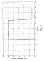
- FIG. 6graphically illustrates a diameter scan of a wafer measuring resist thickness difference (amount of resist removed for a given time) as a function of distance from a centerpoint of a substrate for an ashing process in a plasma asher employing one embodiment of the single baffle and impingement device apparatus in accordance with the present disclosure—an aluminum gas distribution plate assembly, as compared to a prior art dual baffle plate assembly; and
- FIG. 7graphically illustrates endpoint signal as a function of time for an ashing process in a plasma asher employing a second embodiment of the single baffle and impingement device apparatus in accordance with the present disclosure—a quartz gas distribution plate assembly.
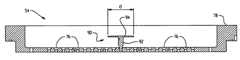
- FIG. 1discloses a photoresist asher 10 , comprising a gas box 12 ; a microwave plasma generator assembly 14 ; a process chamber 16 defining an interior cavity in which is heated a semiconductor substrate such as a wafer 18 ; and a radiant heater assembly 20 for heating the wafer 18 , situated at the bottom of the process chamber.
- a temperature probe 24such as a thermocouple, is used to monitor the temperature of the wafer 18 (also referred to herein as the substrate).
- a vacuum pump 26is used to evacuate the process chamber 16 for processes requiring vacuum conditions.
- microwave plasma generator assemblyother plasma generators are suitable for use in the present disclosure, such as for example, radiofrequency (RF) plasma generators, inductively coupled plasma generators, combination RF and microwave plasma generators, and the like Additionally, while reference is made to radiant heating of the substrate, other heating mechanisms like ultra-violet energy, or hot plates (known as heating chucks) may also be employed. The present disclosure is not intended to be limited to any particular plasma generator or substrate heating mechanism.
- RFradiofrequency
- a monochromator 28is used to monitor the optical emission characteristics of gases within the chamber to aid in process endpoint determination.
- the wafer 18is introduced into and removed from the process chamber via an appropriate load lock mechanism (not shown) via entry/exit passageway 30 .
- load lock mechanismnot shown
- entry/exit passageway 30entry/exit passageway 30 .
- a desired mixture of gasesis introduced into a plasma tube 32 from gas box 12 through an inlet conduit 34 .
- the plasma tube 32is preferably made of alumina (Al 2 O 3 ) or sapphire to accommodate fluorine chemistries without etching or other degradation. In applications where fluorine is not to be used, the plasma tube could be made of quartz.
- the gases forming the desired mixtureare stored in separate supplies (not shown) and mixed in the gas box 12 by means of valves 36 and piping 38 .
- One example of a commonly used gas mixtureis forming gas (primarily nitrogen with a small percentage of hydrogen), and oxygen.
- a fluorine containing gassuch as carbon tetrafluoride (CF 4 ) may also be added to the gas mixture to increase ashing rates for certain processes.
- the gas mixtureis energized by the microwave plasma generator assembly 14 to form reactive plasma that will ash photoresist on the wafer 18 in the process chamber 16 when heated by the radiant heater assembly 20 .
- a magnetron 40generates microwave energy that is coupled to a waveguide 42 . Microwave energy is fed from the waveguide through apertures (not shown) in microwave enclosure 44 , which surrounds the plasma tube 32 .
- An outer quartz cooling tube 46surrounds the plasma tube 32 , slightly separated therefrom. Pressurized air is fed into the gap between the tubes 32 and 46 to effectively cool the tube 32 during operation. Alternately, cooling liquids that do not absorb microwave radiation may be used in place of the pressurized air.
- the microwave enclosure 44is segmented into sections shown by phantom lines 45 . Segmentation of the enclosure 44 allows uniform microwave power distribution across the length of the quartz, alumina or sapphire plasma tube 32 , and protects it from overheating by preventing an unacceptably large thermal gradient from developing along its axial length when suitable input power is provided. Each segment of the enclosure 44 is separately fed with microwave energy that passes through the quartz tube 46 and the alumna or sapphire tube 32 passing therethrough.
- the gas mixture within the plasma tube 32is energized to create plasma.
- Microwave traps 48 and 50are provided at the ends of the microwave enclosure 44 to prevent microwave leakage. Energized plasma enters the process chamber 16 through an opening 51 in the top wall 52 thereof.
- the gas distribution plate assembly 54Positioned between the top wall 52 of the plasma chamber 16 and the wafer 18 being processed is a gas distribution plate assembly 54 (also referred to as baffle plate assembly).
- the gas distribution plate assembly 54provides means for cooling the gases within the plasma to achieve desired process results.
- the baffle plate assembly 54comprises a generally planar gas distribution central portion 74 having apertures 76 therein, surrounded by a flange 78 , and an impingement device 90 attached to the gas distribution central portion 74 .
- the flange 78surrounds the central portion and seats intermediate the process chamber sidewall 53 and top wall 52 . Seals 79 and 81 , respectively, provide airtight connections between the flange 78 and the sidewall 53 , and between the flange 78 and the top wall 52 .
- the seals 79 and 81reside in grooves located in the flange 78 .
- the flange 78also provides mounting holes for mounting to the top wall 52 and sidewall 53 .
- the impingement device 90generally includes a stem portion 92 having one end fixedly attached to the gas distribution central portion 74 and an apertureless cap 94 that is attached to the other end of the stem (shown more clearly in FIG. 3 ).
- the cap 94is preferably dimensioned to prevent direct impingement of plasma from the plasma generator onto the substrate 18 as well as to protect the substrate from line of sight exposure to UV light produced during plasma generation.
- the caphas a diameter “d” that is slightly greater than or at about the same diameter as the opening 51 of the plasma chamber.
- the gas distribution plate assembly 54Positioned between the top wall 52 of the plasma chamber 16 and the wafer 18 being processed is a gas distribution plate assembly 54 (also referred to as baffle plate assembly).
- the gas distribution plate assembly 54provides means for cooling the gases within the plasma to achieve desired process results.
- the baffle plate assembly 54comprises a generally planar gas distribution central portion 74 (also referred to herein as the gas distribution portion) having apertures 76 therein, surrounded by a flange 78 , and an impingement device 90 attached to the gas distribution central portion 74 .
- the flange 78surrounds the central portion and seats intermediate the process chamber sidewall 53 and top wall 52 .
- Seals 79 and 81respectively, provide airtight connections between the flange 78 and the sidewall 53 , and between the flange 78 and the top wall 52 .
- the seals 79 and 81reside in grooves located in the flange 78 .
- the flange 78also provides mounting holes for mounting to the top wall 52 and sidewall 53 .
- the cooling passages 80may extend from the flange 78 into and about the central portion 74 in a configuration that avoids intersection with any of the apertures 76 . Still further, the cooling passages 80 may also extend into the process chamber top wall, if desired.
- These individual cooling subsystems of these structural componentsi.e., baffle plate, side walls and top wall
- the cooling subsystemsmay either share a single gas or liquid coolant circulating system, or may be provided with independent circulating systems (gas or liquid) so as to provide independent temperature control and individual flow control thereof.
- active cooling of the process chamber side walls and top wallare also provided, by maintaining these chamber surfaces at between about 15° C. to about 30° C. (just above the dew point), the wafer 18 can remain sufficiently cool to prevent photoresist popping during, for example, high-density ion implanted wafer ash processes.
- the radiant heater assembly 20comprises a plurality of tungsten halogen lamps 58 residing in a reflector 56 that reflects and redirects the heat generated by the lamps toward the backside of the wafer 18 positioned within the process chamber 16 on quartz or ceramic pins 68 .
- One or more temperature sensors 72are mounted on the interior of process chamber sidewall 53 to provide an indication of wall temperature.
- the baffle plate assembly 54 shown in the photoresist asher 10 of FIG. 1is shown in greater detail in FIG. 3 .
- the baffle plate 54generally comprises the planar central apertured portion 74 and the flange 78 .
- the impingement device 90Located at the center of the planar central apertured portion 74 is the impingement device 90 .
- the impingement device 90diverts energized gases emanating from the plasma tube 32 radially outward to the remaining apertured area of the central apertured portion 74 , so as to prevent direct impingement of atomic species on the wafer 18 being processed and also to prevent overheating of the planar central apertured portion 74 that would result without the impingement device 90 .
- the impingement device 90includes a cap portion 94 and a stem portion 92 .
- the cap 94is spaced apart from the central apertured portion 74 so as to minimize heat transfer to the central apertured portion 74 that may occur from direct plasma impingement.
- the cap 94includes a generally planar impingement surface.
- the stem portion 92is removably attached to the central apertured portion 74 so as to provide ease of replacement if repairs are necessary.
- the stem 92may include a threaded portion and be threadingly mated to a complementary threaded opening in the planar central apertured portion 74 .
- the stem 92is actively cooled during operation by the cooling passages 80 provided in the central apertured portion 74 so as to further minimize heat transfer from the cap 94 to the central apertured portion 74 .
- the single baffle plate assembly 54 with a small impingement device in place of a full size first baffle plateminimizes the surfaces available for species recombination, thereby permitting lower gas flows, and lower pressures while maintaining equivalent ashing rates and uniformities. This represents a significant commercial advantage over the prior art. For example, smaller pumps and vacuum lines can now be used.
- each one of the apertures 76 in the central apertured portion 74preferably includes a frustoconical shaped portion facing the top wall 52 and a substantially straight shaped portion facing the substrate 18 .
- the angle ⁇ defining the frustoconical portionis preferably about 30 to about 60 degrees. In a preferred embodiment, the angle ⁇ defining the frustoconical portion is at about 45 degrees.
- pressureis greater in the space generally defined by the top wall 52 and the central apertured portion 74 than the space generally defined by the central apertured portion 74 and the substrate 18 , thereby providing a downward flow of reactive species onto the substrate.
- the use of lower operating pressurescan be used and still maintain a sufficient pressure differential so as to provide uniform ashing rates across the substrate 18 .
- the single baffle plate and impingement device assembly 54are fabricated from aluminum.
- Suitable aluminum alloysare C-276 commercially available from Alcoa, Incorporated.
- thiseliminates problems noted in the prior art with regard to sapphire coated quartz materials, which tend to flake off during prolonged operation.
- fabricating the impingement device 90 from aluminumeliminates the problems associated with breakage of the ceramic impingement plates noted in the prior art.
- the use of aluminumblocks a large percentage of ultraviolet radiation from impacting the substrate, which would otherwise make temperature control more difficult and possibly cause wafer device damage. Operating at a uniform surface temperature and minimizing exposure to UV radiation provides a substantial improvement in reaction rate uniformity across the surface of the wafer.
- maintaining a consistent baffle plate temperatureeliminates the “first wafer effects” due to parasitic heating of the baffle plate as successive wafers are placed in the process chamber and heated to process temperature by the radiant heating system.
- the single baffle plate and impingement device assembly 54are fabricated from quartz or fused silica.
- quartzreduces manufacturing costs relative to the use of ultra pure aluminum alloys.
- the impingement device 90includes a cap 96 that has an angled surface relative to the axial flow of atomic species from the plasma tube 32 into the process chamber.
- a cross sectional profile of the capis generally triangular shaped and is preferably dimensioned so as to prevent direct ion impingement onto the underlying substrate 18 . That is, diameter “d” is about the same as or slightly greater than the diameter provided by opening 51 .
- this embodimentshows a substantially triangular cross-section, other designs such as a generally concave surface or a generally convex surface could also be used.
- ashing ratewas measured for photoresist ashed using a conventional dual baffle plate design and compared to that for the same tool configured with a single aluminum baffle plate and impingement device assembly as shown in FIG. 3 .
- the baffle plate assemblywas positioned in the process chamber such that the apertured portion was at about the same position as the lower baffle plate in the commercial asher.
- the plasma asherwas model number RadiantStrip 320i commercially available from Axcelis Technologies, Incorporated, which included the conventional dual baffle plate assembly.
- the conventional dual baffle plate assemblywas completely removed and replaced with the single aluminum baffle plate and impingement device assembly. Process conditions and photoresist were identical for each configured system with exceptions noted with regard to gas flow and operating pressure.
- FIG. 6graphically illustrates diameter scans of resist removal rates for the standard flow of 10 slm to the flow of 4 slm.
- ashing ratewas compared for photoresist ashed using a conventional dual baffle design and the same tool configured with the single baffle plate assembly fabricated from quartz and an impingement device.
- the quartz baffle plate and impingement device assemblywas positioned in the process chamber such that the apertured portion was at about the same position as the upper baffle plate in the commercial asher and was not water cooled.
- five blank uncoated substrateswere processed prior to ashing substrate containing the photoresist so as to bring the chamber to thermal equilibrium prior to starting the ash process. Table 2 provides the results.
- FIG. 7graphically illustrates an endpoint trace for the quartz baffle plate assembly.
- the sharp drop at about 32 seconds in the endpoint trace when ashing started at about 15 secondsindicates a very uniform removal of the photoresist, with a time to clear resist of about 17-18 seconds.
- either of the two single baffle plate assemblies including the central apertured portion and the integrated impingement device disclosed hereindo not sacrifice process performance compared to conventional two baffle plate designs.
- Relatively uniform ashing rateswere achieved without significant optimization and it is believed that the single baffle plate assemblies provided herein promote uniform temperature profile across the substrate during plasma ashing.
- Both the quartz and the aluminum baffle plate assembliespermit lower gas flows; lower operating pressures; significantly reduced gas mixing costs; and solves some of the problems currently being encountered. Because of this, smaller pumps and vacuum lines can be employed leading to further cost reductions.
- by minimizing the internal surface area that contacts the plasma during plasma ashing as provided by the gas distribution assemblies illustrated in FIGS. 3 and 4surface recombination of species is minimized.
Landscapes
- Engineering & Computer Science (AREA)
- Physics & Mathematics (AREA)
- Plasma & Fusion (AREA)
- Chemical & Material Sciences (AREA)
- Analytical Chemistry (AREA)
- Toxicology (AREA)
- Health & Medical Sciences (AREA)
- Condensed Matter Physics & Semiconductors (AREA)
- General Physics & Mathematics (AREA)
- Manufacturing & Machinery (AREA)
- Computer Hardware Design (AREA)
- Microelectronics & Electronic Packaging (AREA)
- Power Engineering (AREA)
- Drying Of Semiconductors (AREA)
Abstract
Description
| TABLE 1 | |||||
| Total | |||||
| Gas | Ashing Rate | Non- | |||
| Flow | Pressure | Power | (microns/ | uniformity | |
| Configuration | (slm) | (Torr) | (kilowatt) | minute) | (%) |
| 10 | 1.2 | 3.8 | 7.34 | 4.41 | |
| Plate | |||||
| Single Baffle | 4 | 0.8 | 3.8 | 7.35 | 4.21 |
| Aluminum | |||||
| TABLE 2 | |||||
| Total | |||||
| Gas | Ashing Rate | Non- | |||
| Flow | Pressure | Power | (microns/ | uniformity | |
| Configuration | (slm) | (Torr) | (kilowatt) | minute) | (%) |
| 10 | 1.2 | 3.8 | 6.51 | 5.73 | |
| Single Baffle | |||||
| 5 | 1.2 | 3.8 | 6.73 | 3.31 | |
| Aluminum | |||||
Claims (26)
Priority Applications (7)
| Application Number | Priority Date | Filing Date | Title |
|---|---|---|---|
| US10/755,617US7892357B2 (en) | 2004-01-12 | 2004-01-12 | Gas distribution plate assembly for plasma reactors |
| PCT/US2005/001004WO2005069344A2 (en) | 2004-01-12 | 2005-01-12 | Gas distribution plate assembly for plasma reactors |
| EP05711387AEP1706889B1 (en) | 2004-01-12 | 2005-01-12 | Gas distribution plate assembly for plasma reactors |
| JP2006549575AJP2007520880A (en) | 2004-01-12 | 2005-01-12 | Gas distribution plate assembly for plasma reactor |
| CN2005800021878ACN1910726B (en) | 2004-01-12 | 2005-01-12 | Gas distribution plate assembly for plasma reactors |
| DE602005019535TDE602005019535D1 (en) | 2004-01-12 | 2005-01-12 | GAS DISTRIBUTION PLATE ASSEMBLY FOR PLASMA ACTORS |
| KR1020067014003AKR101258287B1 (en) | 2004-01-12 | 2005-01-12 | Gas distribution plate assembly for plasma reactors |
Applications Claiming Priority (1)
| Application Number | Priority Date | Filing Date | Title |
|---|---|---|---|
| US10/755,617US7892357B2 (en) | 2004-01-12 | 2004-01-12 | Gas distribution plate assembly for plasma reactors |
Publications (2)
| Publication Number | Publication Date |
|---|---|
| US20050150601A1 US20050150601A1 (en) | 2005-07-14 |
| US7892357B2true US7892357B2 (en) | 2011-02-22 |
Family
ID=34739610
Family Applications (1)
| Application Number | Title | Priority Date | Filing Date |
|---|---|---|---|
| US10/755,617Expired - Fee RelatedUS7892357B2 (en) | 2004-01-12 | 2004-01-12 | Gas distribution plate assembly for plasma reactors |
Country Status (7)
| Country | Link |
|---|---|
| US (1) | US7892357B2 (en) |
| EP (1) | EP1706889B1 (en) |
| JP (1) | JP2007520880A (en) |
| KR (1) | KR101258287B1 (en) |
| CN (1) | CN1910726B (en) |
| DE (1) | DE602005019535D1 (en) |
| WO (1) | WO2005069344A2 (en) |
Cited By (13)
| Publication number | Priority date | Publication date | Assignee | Title |
|---|---|---|---|---|
| US20090246374A1 (en)* | 2008-03-28 | 2009-10-01 | Tokyo Electron Limited | Gas distribution system and method for distributing process gas in a processing system |
| US20120055402A1 (en)* | 2009-03-31 | 2012-03-08 | Tokyo Electron Limited | Processing apparatus |
| US20130025787A1 (en)* | 2011-07-25 | 2013-01-31 | Seung-Kook Yang | Baffle and substrate treating apparatuses including the same |
| US20130056022A1 (en)* | 2004-06-24 | 2013-03-07 | Lam Research Corporation | Bare aluminum baffles for resist stripping chambers |
| US8883026B2 (en) | 2012-03-29 | 2014-11-11 | SCREEN Holdings Co., Ltd. | Substrate processing method and substrate processing apparatus |
| US9879795B2 (en) | 2016-01-15 | 2018-01-30 | Lam Research Corporation | Additively manufactured gas distribution manifold |
| US10022689B2 (en) | 2015-07-24 | 2018-07-17 | Lam Research Corporation | Fluid mixing hub for semiconductor processing tool |
| US10118263B2 (en) | 2015-09-02 | 2018-11-06 | Lam Researech Corporation | Monolithic manifold mask and substrate concepts |
| US10128087B2 (en) | 2014-04-07 | 2018-11-13 | Lam Research Corporation | Configuration independent gas delivery system |
| US10215317B2 (en) | 2016-01-15 | 2019-02-26 | Lam Research Corporation | Additively manufactured gas distribution manifold |
| US10351955B2 (en) | 2013-12-18 | 2019-07-16 | Lam Research Corporation | Semiconductor substrate processing apparatus including uniformity baffles |
| US10557197B2 (en) | 2014-10-17 | 2020-02-11 | Lam Research Corporation | Monolithic gas distribution manifold and various construction techniques and use cases therefor |
| USD1080812S1 (en) | 2022-08-29 | 2025-06-24 | Applied Materials, Inc. | Gas mixer |
Families Citing this family (306)
| Publication number | Priority date | Publication date | Assignee | Title |
|---|---|---|---|---|
| CN101053063B (en)* | 2004-09-01 | 2012-10-03 | 艾克塞利斯技术公司 | Apparatus and plasma ashing method for increasing photoresist removal rate |
| JP2006128485A (en)* | 2004-10-29 | 2006-05-18 | Asm Japan Kk | Semiconductor processing apparatus |
| US20060228889A1 (en)* | 2005-03-31 | 2006-10-12 | Edelberg Erik A | Methods of removing resist from substrates in resist stripping chambers |
| JP2009518854A (en)* | 2005-12-07 | 2009-05-07 | アクセリス テクノロジーズ インコーポレーテッド | Medium pressure plasma system for surface layer removal without substrate loss |
| US8034176B2 (en)* | 2006-03-28 | 2011-10-11 | Tokyo Electron Limited | Gas distribution system for a post-etch treatment system |
| JP2008205219A (en)* | 2007-02-20 | 2008-09-04 | Masato Toshima | Showerhead, and cvd apparatus using the same showerhead |
| WO2008114363A1 (en)* | 2007-03-16 | 2008-09-25 | Fujitsu Microelectronics Limited | Apparatus for producing semiconductor device and process for producing semiconductor device |
| KR100997104B1 (en) | 2008-07-04 | 2010-11-29 | 주식회사 테스 | Shower head for semiconductor manufacturing and semiconductor manufacturing apparatus provided with this shower head |
| KR101046335B1 (en)* | 2008-07-29 | 2011-07-05 | 피에스케이 주식회사 | Hollow cathode plasma generation method and large area substrate processing method using hollow cathode plasma |
| US20100130017A1 (en)* | 2008-11-21 | 2010-05-27 | Axcelis Technologies, Inc. | Front end of line plasma mediated ashing processes and apparatus |
| US20110226280A1 (en)* | 2008-11-21 | 2011-09-22 | Axcelis Technologies, Inc. | Plasma mediated ashing processes |
| JP5835722B2 (en) | 2009-12-10 | 2015-12-24 | オルボテック エルティ ソラー,エルエルシー | Automatic ranking multi-directional serial processor |
| CN102127757A (en)* | 2011-01-14 | 2011-07-20 | 映瑞光电科技(上海)有限公司 | Metal organic chemical vapor deposition (MOCVD) reaction system |
| US8802545B2 (en)* | 2011-03-14 | 2014-08-12 | Plasma-Therm Llc | Method and apparatus for plasma dicing a semi-conductor wafer |
| US8459276B2 (en) | 2011-05-24 | 2013-06-11 | Orbotech LT Solar, LLC. | Broken wafer recovery system |
| US20130023129A1 (en) | 2011-07-20 | 2013-01-24 | Asm America, Inc. | Pressure transmitter for a semiconductor processing environment |
| US9947512B2 (en)* | 2011-10-25 | 2018-04-17 | Lam Research Corporation | Window and mounting arrangement for twist-and-lock gas injector assembly of inductively coupled plasma chamber |
| CN103103499A (en)* | 2011-11-11 | 2013-05-15 | 中国科学院沈阳科学仪器研制中心有限公司 | Labyrinth air-inlet device for vacuum chamber of large plate-type PECVD (plasma enhanced chemical vapor deposition) apparatus |
| US10714315B2 (en) | 2012-10-12 | 2020-07-14 | Asm Ip Holdings B.V. | Semiconductor reaction chamber showerhead |
| US20160376700A1 (en) | 2013-02-01 | 2016-12-29 | Asm Ip Holding B.V. | System for treatment of deposition reactor |
| US10683571B2 (en)* | 2014-02-25 | 2020-06-16 | Asm Ip Holding B.V. | Gas supply manifold and method of supplying gases to chamber using same |
| US11015245B2 (en) | 2014-03-19 | 2021-05-25 | Asm Ip Holding B.V. | Gas-phase reactor and system having exhaust plenum and components thereof |
| US10941490B2 (en) | 2014-10-07 | 2021-03-09 | Asm Ip Holding B.V. | Multiple temperature range susceptor, assembly, reactor and system including the susceptor, and methods of using the same |
| CN105590825A (en)* | 2014-11-03 | 2016-05-18 | 中微半导体设备(上海)有限公司 | Gas conveying apparatus and plasma processing apparatus |
| US20160177442A1 (en)* | 2014-12-18 | 2016-06-23 | Ervin Beloni | Gas shield for vapor deposition |
| US10276355B2 (en) | 2015-03-12 | 2019-04-30 | Asm Ip Holding B.V. | Multi-zone reactor, system including the reactor, and method of using the same |
| CN104894533B (en)* | 2015-04-01 | 2017-10-03 | 沈阳拓荆科技有限公司 | A kind of star heat transfer medium channels structure of semiconductor equipment temperature control spray equipment |
| US11384432B2 (en) | 2015-04-22 | 2022-07-12 | Applied Materials, Inc. | Atomic layer deposition chamber with funnel-shaped gas dispersion channel and gas distribution plate |
| US10458018B2 (en) | 2015-06-26 | 2019-10-29 | Asm Ip Holding B.V. | Structures including metal carbide material, devices including the structures, and methods of forming same |
| US10211308B2 (en) | 2015-10-21 | 2019-02-19 | Asm Ip Holding B.V. | NbMC layers |
| US11139308B2 (en) | 2015-12-29 | 2021-10-05 | Asm Ip Holding B.V. | Atomic layer deposition of III-V compounds to form V-NAND devices |
| US10529554B2 (en) | 2016-02-19 | 2020-01-07 | Asm Ip Holding B.V. | Method for forming silicon nitride film selectively on sidewalls or flat surfaces of trenches |
| US10343920B2 (en) | 2016-03-18 | 2019-07-09 | Asm Ip Holding B.V. | Aligned carbon nanotubes |
| US10367080B2 (en) | 2016-05-02 | 2019-07-30 | Asm Ip Holding B.V. | Method of forming a germanium oxynitride film |
| US11453943B2 (en) | 2016-05-25 | 2022-09-27 | Asm Ip Holding B.V. | Method for forming carbon-containing silicon/metal oxide or nitride film by ALD using silicon precursor and hydrocarbon precursor |
| US9859151B1 (en) | 2016-07-08 | 2018-01-02 | Asm Ip Holding B.V. | Selective film deposition method to form air gaps |
| US10612137B2 (en) | 2016-07-08 | 2020-04-07 | Asm Ip Holdings B.V. | Organic reactants for atomic layer deposition |
| US9812320B1 (en) | 2016-07-28 | 2017-11-07 | Asm Ip Holding B.V. | Method and apparatus for filling a gap |
| US9887082B1 (en) | 2016-07-28 | 2018-02-06 | Asm Ip Holding B.V. | Method and apparatus for filling a gap |
| KR102532607B1 (en) | 2016-07-28 | 2023-05-15 | 에이에스엠 아이피 홀딩 비.브이. | Substrate processing apparatus and method of operating the same |
| US11532757B2 (en) | 2016-10-27 | 2022-12-20 | Asm Ip Holding B.V. | Deposition of charge trapping layers |
| US10714350B2 (en) | 2016-11-01 | 2020-07-14 | ASM IP Holdings, B.V. | Methods for forming a transition metal niobium nitride film on a substrate by atomic layer deposition and related semiconductor device structures |
| KR102546317B1 (en) | 2016-11-15 | 2023-06-21 | 에이에스엠 아이피 홀딩 비.브이. | Gas supply unit and substrate processing apparatus including the same |
| KR102762543B1 (en) | 2016-12-14 | 2025-02-05 | 에이에스엠 아이피 홀딩 비.브이. | Substrate processing apparatus |
| US11447861B2 (en) | 2016-12-15 | 2022-09-20 | Asm Ip Holding B.V. | Sequential infiltration synthesis apparatus and a method of forming a patterned structure |
| US11581186B2 (en) | 2016-12-15 | 2023-02-14 | Asm Ip Holding B.V. | Sequential infiltration synthesis apparatus |
| KR102700194B1 (en) | 2016-12-19 | 2024-08-28 | 에이에스엠 아이피 홀딩 비.브이. | Substrate processing apparatus |
| US11694911B2 (en) | 2016-12-20 | 2023-07-04 | Lam Research Corporation | Systems and methods for metastable activated radical selective strip and etch using dual plenum showerhead |
| US10269558B2 (en) | 2016-12-22 | 2019-04-23 | Asm Ip Holding B.V. | Method of forming a structure on a substrate |
| US11390950B2 (en) | 2017-01-10 | 2022-07-19 | Asm Ip Holding B.V. | Reactor system and method to reduce residue buildup during a film deposition process |
| US9934933B1 (en)* | 2017-01-19 | 2018-04-03 | Kla-Tencor Corporation | Extractor electrode for electron source |
| US10468261B2 (en) | 2017-02-15 | 2019-11-05 | Asm Ip Holding B.V. | Methods for forming a metallic film on a substrate by cyclical deposition and related semiconductor device structures |
| US10529563B2 (en) | 2017-03-29 | 2020-01-07 | Asm Ip Holdings B.V. | Method for forming doped metal oxide films on a substrate by cyclical deposition and related semiconductor device structures |
| JP6899693B2 (en)* | 2017-04-14 | 2021-07-07 | 東京エレクトロン株式会社 | Plasma processing equipment and control method |
| US10770286B2 (en) | 2017-05-08 | 2020-09-08 | Asm Ip Holdings B.V. | Methods for selectively forming a silicon nitride film on a substrate and related semiconductor device structures |
| US12040200B2 (en) | 2017-06-20 | 2024-07-16 | Asm Ip Holding B.V. | Semiconductor processing apparatus and methods for calibrating a semiconductor processing apparatus |
| US11306395B2 (en) | 2017-06-28 | 2022-04-19 | Asm Ip Holding B.V. | Methods for depositing a transition metal nitride film on a substrate by atomic layer deposition and related deposition apparatus |
| KR20190009245A (en) | 2017-07-18 | 2019-01-28 | 에이에스엠 아이피 홀딩 비.브이. | Methods for forming a semiconductor device structure and related semiconductor device structures |
| US10541333B2 (en) | 2017-07-19 | 2020-01-21 | Asm Ip Holding B.V. | Method for depositing a group IV semiconductor and related semiconductor device structures |
| US11018002B2 (en) | 2017-07-19 | 2021-05-25 | Asm Ip Holding B.V. | Method for selectively depositing a Group IV semiconductor and related semiconductor device structures |
| US11374112B2 (en) | 2017-07-19 | 2022-06-28 | Asm Ip Holding B.V. | Method for depositing a group IV semiconductor and related semiconductor device structures |
| US10590535B2 (en) | 2017-07-26 | 2020-03-17 | Asm Ip Holdings B.V. | Chemical treatment, deposition and/or infiltration apparatus and method for using the same |
| TWI815813B (en) | 2017-08-04 | 2023-09-21 | 荷蘭商Asm智慧財產控股公司 | Showerhead assembly for distributing a gas within a reaction chamber |
| US10770336B2 (en) | 2017-08-08 | 2020-09-08 | Asm Ip Holding B.V. | Substrate lift mechanism and reactor including same |
| US10692741B2 (en) | 2017-08-08 | 2020-06-23 | Asm Ip Holdings B.V. | Radiation shield |
| US11139191B2 (en) | 2017-08-09 | 2021-10-05 | Asm Ip Holding B.V. | Storage apparatus for storing cassettes for substrates and processing apparatus equipped therewith |
| US11769682B2 (en) | 2017-08-09 | 2023-09-26 | Asm Ip Holding B.V. | Storage apparatus for storing cassettes for substrates and processing apparatus equipped therewith |
| US11830730B2 (en) | 2017-08-29 | 2023-11-28 | Asm Ip Holding B.V. | Layer forming method and apparatus |
| US11295980B2 (en) | 2017-08-30 | 2022-04-05 | Asm Ip Holding B.V. | Methods for depositing a molybdenum metal film over a dielectric surface of a substrate by a cyclical deposition process and related semiconductor device structures |
| US11056344B2 (en) | 2017-08-30 | 2021-07-06 | Asm Ip Holding B.V. | Layer forming method |
| KR102491945B1 (en) | 2017-08-30 | 2023-01-26 | 에이에스엠 아이피 홀딩 비.브이. | Substrate processing apparatus |
| US20190070639A1 (en)* | 2017-09-07 | 2019-03-07 | Applied Materials, Inc. | Automatic cleaning machine for cleaning process kits |
| US10658205B2 (en) | 2017-09-28 | 2020-05-19 | Asm Ip Holdings B.V. | Chemical dispensing apparatus and methods for dispensing a chemical to a reaction chamber |
| US10872789B2 (en)* | 2017-09-28 | 2020-12-22 | Taiwan Semiconductor Manufacturing Co., Ltd. | Wafer cooling system |
| US10403504B2 (en) | 2017-10-05 | 2019-09-03 | Asm Ip Holding B.V. | Method for selectively depositing a metallic film on a substrate |
| US10923344B2 (en) | 2017-10-30 | 2021-02-16 | Asm Ip Holding B.V. | Methods for forming a semiconductor structure and related semiconductor structures |
| US11022879B2 (en) | 2017-11-24 | 2021-06-01 | Asm Ip Holding B.V. | Method of forming an enhanced unexposed photoresist layer |
| CN111344522B (en) | 2017-11-27 | 2022-04-12 | 阿斯莫Ip控股公司 | Including clean mini-environment device |
| WO2019103613A1 (en) | 2017-11-27 | 2019-05-31 | Asm Ip Holding B.V. | A storage device for storing wafer cassettes for use with a batch furnace |
| US10872771B2 (en) | 2018-01-16 | 2020-12-22 | Asm Ip Holding B. V. | Method for depositing a material film on a substrate within a reaction chamber by a cyclical deposition process and related device structures |
| TWI799494B (en) | 2018-01-19 | 2023-04-21 | 荷蘭商Asm 智慧財產控股公司 | Deposition method |
| KR102695659B1 (en) | 2018-01-19 | 2024-08-14 | 에이에스엠 아이피 홀딩 비.브이. | Method for depositing a gap filling layer by plasma assisted deposition |
| US11081345B2 (en) | 2018-02-06 | 2021-08-03 | Asm Ip Holding B.V. | Method of post-deposition treatment for silicon oxide film |
| WO2019158960A1 (en) | 2018-02-14 | 2019-08-22 | Asm Ip Holding B.V. | A method for depositing a ruthenium-containing film on a substrate by a cyclical deposition process |
| US10896820B2 (en) | 2018-02-14 | 2021-01-19 | Asm Ip Holding B.V. | Method for depositing a ruthenium-containing film on a substrate by a cyclical deposition process |
| US10731249B2 (en) | 2018-02-15 | 2020-08-04 | Asm Ip Holding B.V. | Method of forming a transition metal containing film on a substrate by a cyclical deposition process, a method for supplying a transition metal halide compound to a reaction chamber, and related vapor deposition apparatus |
| KR102636427B1 (en) | 2018-02-20 | 2024-02-13 | 에이에스엠 아이피 홀딩 비.브이. | Substrate processing method and apparatus |
| US10975470B2 (en) | 2018-02-23 | 2021-04-13 | Asm Ip Holding B.V. | Apparatus for detecting or monitoring for a chemical precursor in a high temperature environment |
| US11473195B2 (en) | 2018-03-01 | 2022-10-18 | Asm Ip Holding B.V. | Semiconductor processing apparatus and a method for processing a substrate |
| US11629406B2 (en) | 2018-03-09 | 2023-04-18 | Asm Ip Holding B.V. | Semiconductor processing apparatus comprising one or more pyrometers for measuring a temperature of a substrate during transfer of the substrate |
| US11114283B2 (en) | 2018-03-16 | 2021-09-07 | Asm Ip Holding B.V. | Reactor, system including the reactor, and methods of manufacturing and using same |
| KR102646467B1 (en) | 2018-03-27 | 2024-03-11 | 에이에스엠 아이피 홀딩 비.브이. | Method of forming an electrode on a substrate and a semiconductor device structure including an electrode |
| US11088002B2 (en) | 2018-03-29 | 2021-08-10 | Asm Ip Holding B.V. | Substrate rack and a substrate processing system and method |
| US11230766B2 (en) | 2018-03-29 | 2022-01-25 | Asm Ip Holding B.V. | Substrate processing apparatus and method |
| KR102600229B1 (en) | 2018-04-09 | 2023-11-10 | 에이에스엠 아이피 홀딩 비.브이. | Substrate supporting device, substrate processing apparatus including the same and substrate processing method |
| TWI811348B (en) | 2018-05-08 | 2023-08-11 | 荷蘭商Asm 智慧財產控股公司 | Methods for depositing an oxide film on a substrate by a cyclical deposition process and related device structures |
| US12025484B2 (en) | 2018-05-08 | 2024-07-02 | Asm Ip Holding B.V. | Thin film forming method |
| US12272527B2 (en) | 2018-05-09 | 2025-04-08 | Asm Ip Holding B.V. | Apparatus for use with hydrogen radicals and method of using same |
| KR102596988B1 (en) | 2018-05-28 | 2023-10-31 | 에이에스엠 아이피 홀딩 비.브이. | Method of processing a substrate and a device manufactured by the same |
| US11718913B2 (en) | 2018-06-04 | 2023-08-08 | Asm Ip Holding B.V. | Gas distribution system and reactor system including same |
| TWI840362B (en) | 2018-06-04 | 2024-05-01 | 荷蘭商Asm Ip私人控股有限公司 | Wafer handling chamber with moisture reduction |
| US11286562B2 (en) | 2018-06-08 | 2022-03-29 | Asm Ip Holding B.V. | Gas-phase chemical reactor and method of using same |
| KR102568797B1 (en) | 2018-06-21 | 2023-08-21 | 에이에스엠 아이피 홀딩 비.브이. | Substrate processing system |
| US10797133B2 (en) | 2018-06-21 | 2020-10-06 | Asm Ip Holding B.V. | Method for depositing a phosphorus doped silicon arsenide film and related semiconductor device structures |
| TWI873894B (en) | 2018-06-27 | 2025-02-21 | 荷蘭商Asm Ip私人控股有限公司 | Cyclic deposition methods for forming metal-containing material and films and structures including the metal-containing material |
| KR102854019B1 (en) | 2018-06-27 | 2025-09-02 | 에이에스엠 아이피 홀딩 비.브이. | Periodic deposition method for forming a metal-containing material and films and structures comprising the metal-containing material |
| US10612136B2 (en) | 2018-06-29 | 2020-04-07 | ASM IP Holding, B.V. | Temperature-controlled flange and reactor system including same |
| US10755922B2 (en) | 2018-07-03 | 2020-08-25 | Asm Ip Holding B.V. | Method for depositing silicon-free carbon-containing film as gap-fill layer by pulse plasma-assisted deposition |
| US10388513B1 (en) | 2018-07-03 | 2019-08-20 | Asm Ip Holding B.V. | Method for depositing silicon-free carbon-containing film as gap-fill layer by pulse plasma-assisted deposition |
| US11053591B2 (en) | 2018-08-06 | 2021-07-06 | Asm Ip Holding B.V. | Multi-port gas injection system and reactor system including same |
| US11430674B2 (en) | 2018-08-22 | 2022-08-30 | Asm Ip Holding B.V. | Sensor array, apparatus for dispensing a vapor phase reactant to a reaction chamber and related methods |
| US11024523B2 (en) | 2018-09-11 | 2021-06-01 | Asm Ip Holding B.V. | Substrate processing apparatus and method |
| KR102707956B1 (en) | 2018-09-11 | 2024-09-19 | 에이에스엠 아이피 홀딩 비.브이. | Method for deposition of a thin film |
| US11049751B2 (en) | 2018-09-14 | 2021-06-29 | Asm Ip Holding B.V. | Cassette supply system to store and handle cassettes and processing apparatus equipped therewith |
| CN110970344B (en) | 2018-10-01 | 2024-10-25 | Asmip控股有限公司 | Substrate holding apparatus, system comprising the same and method of using the same |
| US11232963B2 (en) | 2018-10-03 | 2022-01-25 | Asm Ip Holding B.V. | Substrate processing apparatus and method |
| KR102592699B1 (en) | 2018-10-08 | 2023-10-23 | 에이에스엠 아이피 홀딩 비.브이. | Substrate support unit and apparatuses for depositing thin film and processing the substrate including the same |
| KR102605121B1 (en) | 2018-10-19 | 2023-11-23 | 에이에스엠 아이피 홀딩 비.브이. | Substrate processing apparatus and substrate processing method |
| KR102546322B1 (en) | 2018-10-19 | 2023-06-21 | 에이에스엠 아이피 홀딩 비.브이. | Substrate processing apparatus and substrate processing method |
| USD948463S1 (en) | 2018-10-24 | 2022-04-12 | Asm Ip Holding B.V. | Susceptor for semiconductor substrate supporting apparatus |
| US12378665B2 (en) | 2018-10-26 | 2025-08-05 | Asm Ip Holding B.V. | High temperature coatings for a preclean and etch apparatus and related methods |
| US11087997B2 (en) | 2018-10-31 | 2021-08-10 | Asm Ip Holding B.V. | Substrate processing apparatus for processing substrates |
| KR102748291B1 (en) | 2018-11-02 | 2024-12-31 | 에이에스엠 아이피 홀딩 비.브이. | Substrate support unit and substrate processing apparatus including the same |
| US11572620B2 (en) | 2018-11-06 | 2023-02-07 | Asm Ip Holding B.V. | Methods for selectively depositing an amorphous silicon film on a substrate |
| US11031242B2 (en) | 2018-11-07 | 2021-06-08 | Asm Ip Holding B.V. | Methods for depositing a boron doped silicon germanium film |
| US10847366B2 (en) | 2018-11-16 | 2020-11-24 | Asm Ip Holding B.V. | Methods for depositing a transition metal chalcogenide film on a substrate by a cyclical deposition process |
| US10818758B2 (en) | 2018-11-16 | 2020-10-27 | Asm Ip Holding B.V. | Methods for forming a metal silicate film on a substrate in a reaction chamber and related semiconductor device structures |
| US12040199B2 (en) | 2018-11-28 | 2024-07-16 | Asm Ip Holding B.V. | Substrate processing apparatus for processing substrates |
| US11217444B2 (en) | 2018-11-30 | 2022-01-04 | Asm Ip Holding B.V. | Method for forming an ultraviolet radiation responsive metal oxide-containing film |
| KR102636428B1 (en) | 2018-12-04 | 2024-02-13 | 에이에스엠 아이피 홀딩 비.브이. | A method for cleaning a substrate processing apparatus |
| US11158513B2 (en) | 2018-12-13 | 2021-10-26 | Asm Ip Holding B.V. | Methods for forming a rhenium-containing film on a substrate by a cyclical deposition process and related semiconductor device structures |
| TWI874340B (en) | 2018-12-14 | 2025-03-01 | 荷蘭商Asm Ip私人控股有限公司 | Method of forming device structure, structure formed by the method and system for performing the method |
| TWI866480B (en) | 2019-01-17 | 2024-12-11 | 荷蘭商Asm Ip 私人控股有限公司 | Methods of forming a transition metal containing film on a substrate by a cyclical deposition process |
| KR102727227B1 (en) | 2019-01-22 | 2024-11-07 | 에이에스엠 아이피 홀딩 비.브이. | Semiconductor processing device |
| US11967486B2 (en) | 2019-01-23 | 2024-04-23 | Lam Research Corporation | Substrate processing system including dual ion filter for downstream plasma |
| CN111524788B (en) | 2019-02-01 | 2023-11-24 | Asm Ip私人控股有限公司 | Method for forming topologically selective films of silicon oxide |
| TWI838458B (en) | 2019-02-20 | 2024-04-11 | 荷蘭商Asm Ip私人控股有限公司 | Apparatus and methods for plug fill deposition in 3-d nand applications |
| KR102626263B1 (en) | 2019-02-20 | 2024-01-16 | 에이에스엠 아이피 홀딩 비.브이. | Cyclical deposition method including treatment step and apparatus for same |
| TWI873122B (en) | 2019-02-20 | 2025-02-21 | 荷蘭商Asm Ip私人控股有限公司 | Method of filling a recess formed within a surface of a substrate, semiconductor structure formed according to the method, and semiconductor processing apparatus |
| TWI845607B (en) | 2019-02-20 | 2024-06-21 | 荷蘭商Asm Ip私人控股有限公司 | Cyclical deposition method and apparatus for filling a recess formed within a substrate surface |
| TWI842826B (en) | 2019-02-22 | 2024-05-21 | 荷蘭商Asm Ip私人控股有限公司 | Substrate processing apparatus and method for processing substrate |
| KR102858005B1 (en) | 2019-03-08 | 2025-09-09 | 에이에스엠 아이피 홀딩 비.브이. | Method for Selective Deposition of Silicon Nitride Layer and Structure Including Selectively-Deposited Silicon Nitride Layer |
| KR102782593B1 (en) | 2019-03-08 | 2025-03-14 | 에이에스엠 아이피 홀딩 비.브이. | Structure Including SiOC Layer and Method of Forming Same |
| US11742198B2 (en) | 2019-03-08 | 2023-08-29 | Asm Ip Holding B.V. | Structure including SiOCN layer and method of forming same |
| JP2020167398A (en) | 2019-03-28 | 2020-10-08 | エーエスエム・アイピー・ホールディング・ベー・フェー | Door openers and substrate processing equipment provided with door openers |
| KR102809999B1 (en) | 2019-04-01 | 2025-05-19 | 에이에스엠 아이피 홀딩 비.브이. | Method of manufacturing semiconductor device |
| KR20200123380A (en) | 2019-04-19 | 2020-10-29 | 에이에스엠 아이피 홀딩 비.브이. | Layer forming method and apparatus |
| KR20200125453A (en) | 2019-04-24 | 2020-11-04 | 에이에스엠 아이피 홀딩 비.브이. | Gas-phase reactor system and method of using same |
| US11289326B2 (en) | 2019-05-07 | 2022-03-29 | Asm Ip Holding B.V. | Method for reforming amorphous carbon polymer film |
| KR20200130121A (en) | 2019-05-07 | 2020-11-18 | 에이에스엠 아이피 홀딩 비.브이. | Chemical source vessel with dip tube |
| KR20200130652A (en) | 2019-05-10 | 2020-11-19 | 에이에스엠 아이피 홀딩 비.브이. | Method of depositing material onto a surface and structure formed according to the method |
| JP7598201B2 (en) | 2019-05-16 | 2024-12-11 | エーエスエム・アイピー・ホールディング・ベー・フェー | Wafer boat handling apparatus, vertical batch furnace and method |
| JP7612342B2 (en) | 2019-05-16 | 2025-01-14 | エーエスエム・アイピー・ホールディング・ベー・フェー | Wafer boat handling apparatus, vertical batch furnace and method |
| USD975665S1 (en) | 2019-05-17 | 2023-01-17 | Asm Ip Holding B.V. | Susceptor shaft |
| USD947913S1 (en) | 2019-05-17 | 2022-04-05 | Asm Ip Holding B.V. | Susceptor shaft |
| USD935572S1 (en) | 2019-05-24 | 2021-11-09 | Asm Ip Holding B.V. | Gas channel plate |
| USD922229S1 (en) | 2019-06-05 | 2021-06-15 | Asm Ip Holding B.V. | Device for controlling a temperature of a gas supply unit |
| KR20200141002A (en) | 2019-06-06 | 2020-12-17 | 에이에스엠 아이피 홀딩 비.브이. | Method of using a gas-phase reactor system including analyzing exhausted gas |
| KR20200141931A (en) | 2019-06-10 | 2020-12-21 | 에이에스엠 아이피 홀딩 비.브이. | Method for cleaning quartz epitaxial chambers |
| KR20200143254A (en) | 2019-06-11 | 2020-12-23 | 에이에스엠 아이피 홀딩 비.브이. | Method of forming an electronic structure using an reforming gas, system for performing the method, and structure formed using the method |
| USD944946S1 (en) | 2019-06-14 | 2022-03-01 | Asm Ip Holding B.V. | Shower plate |
| USD931978S1 (en) | 2019-06-27 | 2021-09-28 | Asm Ip Holding B.V. | Showerhead vacuum transport |
| KR20210005515A (en) | 2019-07-03 | 2021-01-14 | 에이에스엠 아이피 홀딩 비.브이. | Temperature control assembly for substrate processing apparatus and method of using same |
| JP7499079B2 (en) | 2019-07-09 | 2024-06-13 | エーエスエム・アイピー・ホールディング・ベー・フェー | Plasma device using coaxial waveguide and substrate processing method |
| CN112216646A (en) | 2019-07-10 | 2021-01-12 | Asm Ip私人控股有限公司 | Substrate supporting assembly and substrate processing device comprising same |
| KR20210010307A (en) | 2019-07-16 | 2021-01-27 | 에이에스엠 아이피 홀딩 비.브이. | Substrate processing apparatus |
| KR20210010816A (en) | 2019-07-17 | 2021-01-28 | 에이에스엠 아이피 홀딩 비.브이. | Radical assist ignition plasma system and method |
| KR102860110B1 (en) | 2019-07-17 | 2025-09-16 | 에이에스엠 아이피 홀딩 비.브이. | Methods of forming silicon germanium structures |
| US11643724B2 (en) | 2019-07-18 | 2023-05-09 | Asm Ip Holding B.V. | Method of forming structures using a neutral beam |
| TWI839544B (en) | 2019-07-19 | 2024-04-21 | 荷蘭商Asm Ip私人控股有限公司 | Method of forming topology-controlled amorphous carbon polymer film |
| KR20210010817A (en) | 2019-07-19 | 2021-01-28 | 에이에스엠 아이피 홀딩 비.브이. | Method of Forming Topology-Controlled Amorphous Carbon Polymer Film |
| TWI851767B (en) | 2019-07-29 | 2024-08-11 | 荷蘭商Asm Ip私人控股有限公司 | Methods for selective deposition utilizing n-type dopants and/or alternative dopants to achieve high dopant incorporation |
| CN112309900A (en) | 2019-07-30 | 2021-02-02 | Asm Ip私人控股有限公司 | Substrate processing apparatus |
| US12169361B2 (en) | 2019-07-30 | 2024-12-17 | Asm Ip Holding B.V. | Substrate processing apparatus and method |
| CN112309899A (en) | 2019-07-30 | 2021-02-02 | Asm Ip私人控股有限公司 | Substrate processing apparatus |
| US11587814B2 (en) | 2019-07-31 | 2023-02-21 | Asm Ip Holding B.V. | Vertical batch furnace assembly |
| US11587815B2 (en) | 2019-07-31 | 2023-02-21 | Asm Ip Holding B.V. | Vertical batch furnace assembly |
| US11227782B2 (en) | 2019-07-31 | 2022-01-18 | Asm Ip Holding B.V. | Vertical batch furnace assembly |
| CN112323048B (en) | 2019-08-05 | 2024-02-09 | Asm Ip私人控股有限公司 | Liquid level sensor for chemical source container |
| CN112342526A (en) | 2019-08-09 | 2021-02-09 | Asm Ip私人控股有限公司 | Heater assembly including cooling device and method of using same |
| USD965524S1 (en) | 2019-08-19 | 2022-10-04 | Asm Ip Holding B.V. | Susceptor support |
| USD965044S1 (en) | 2019-08-19 | 2022-09-27 | Asm Ip Holding B.V. | Susceptor shaft |
| JP2021031769A (en) | 2019-08-21 | 2021-03-01 | エーエスエム アイピー ホールディング ビー.ブイ. | Production apparatus of mixed gas of film deposition raw material and film deposition apparatus |
| USD930782S1 (en) | 2019-08-22 | 2021-09-14 | Asm Ip Holding B.V. | Gas distributor |
| USD949319S1 (en) | 2019-08-22 | 2022-04-19 | Asm Ip Holding B.V. | Exhaust duct |
| KR20210024423A (en) | 2019-08-22 | 2021-03-05 | 에이에스엠 아이피 홀딩 비.브이. | Method for forming a structure with a hole |
| USD979506S1 (en) | 2019-08-22 | 2023-02-28 | Asm Ip Holding B.V. | Insulator |
| USD940837S1 (en) | 2019-08-22 | 2022-01-11 | Asm Ip Holding B.V. | Electrode |
| KR20210024420A (en) | 2019-08-23 | 2021-03-05 | 에이에스엠 아이피 홀딩 비.브이. | Method for depositing silicon oxide film having improved quality by peald using bis(diethylamino)silane |
| US11286558B2 (en) | 2019-08-23 | 2022-03-29 | Asm Ip Holding B.V. | Methods for depositing a molybdenum nitride film on a surface of a substrate by a cyclical deposition process and related semiconductor device structures including a molybdenum nitride film |
| KR102806450B1 (en) | 2019-09-04 | 2025-05-12 | 에이에스엠 아이피 홀딩 비.브이. | Methods for selective deposition using a sacrificial capping layer |
| KR102733104B1 (en) | 2019-09-05 | 2024-11-22 | 에이에스엠 아이피 홀딩 비.브이. | Substrate processing apparatus |
| US20220336194A1 (en)* | 2019-09-17 | 2022-10-20 | Tokyo Electron Limited | Plasma processing apparatus |
| US11562901B2 (en) | 2019-09-25 | 2023-01-24 | Asm Ip Holding B.V. | Substrate processing method |
| CN112593212B (en) | 2019-10-02 | 2023-12-22 | Asm Ip私人控股有限公司 | Method for forming topologically selective silicon oxide film by cyclic plasma enhanced deposition process |
| TWI846953B (en) | 2019-10-08 | 2024-07-01 | 荷蘭商Asm Ip私人控股有限公司 | Substrate processing device |
| TW202128273A (en) | 2019-10-08 | 2021-08-01 | 荷蘭商Asm Ip私人控股有限公司 | Gas injection system, reactor system, and method of depositing material on surface of substratewithin reaction chamber |
| KR20210042810A (en) | 2019-10-08 | 2021-04-20 | 에이에스엠 아이피 홀딩 비.브이. | Reactor system including a gas distribution assembly for use with activated species and method of using same |
| TWI846966B (en) | 2019-10-10 | 2024-07-01 | 荷蘭商Asm Ip私人控股有限公司 | Method of forming a photoresist underlayer and structure including same |
| US12009241B2 (en) | 2019-10-14 | 2024-06-11 | Asm Ip Holding B.V. | Vertical batch furnace assembly with detector to detect cassette |
| TWI834919B (en) | 2019-10-16 | 2024-03-11 | 荷蘭商Asm Ip私人控股有限公司 | Method of topology-selective film formation of silicon oxide |
| US11637014B2 (en) | 2019-10-17 | 2023-04-25 | Asm Ip Holding B.V. | Methods for selective deposition of doped semiconductor material |
| KR102845724B1 (en) | 2019-10-21 | 2025-08-13 | 에이에스엠 아이피 홀딩 비.브이. | Apparatus and methods for selectively etching films |
| KR20210050453A (en) | 2019-10-25 | 2021-05-07 | 에이에스엠 아이피 홀딩 비.브이. | Methods for filling a gap feature on a substrate surface and related semiconductor structures |
| US11646205B2 (en) | 2019-10-29 | 2023-05-09 | Asm Ip Holding B.V. | Methods of selectively forming n-type doped material on a surface, systems for selectively forming n-type doped material, and structures formed using same |
| KR20210054983A (en) | 2019-11-05 | 2021-05-14 | 에이에스엠 아이피 홀딩 비.브이. | Structures with doped semiconductor layers and methods and systems for forming same |
| US11501968B2 (en) | 2019-11-15 | 2022-11-15 | Asm Ip Holding B.V. | Method for providing a semiconductor device with silicon filled gaps |
| KR102861314B1 (en) | 2019-11-20 | 2025-09-17 | 에이에스엠 아이피 홀딩 비.브이. | Method of depositing carbon-containing material on a surface of a substrate, structure formed using the method, and system for forming the structure |
| US11450529B2 (en) | 2019-11-26 | 2022-09-20 | Asm Ip Holding B.V. | Methods for selectively forming a target film on a substrate comprising a first dielectric surface and a second metallic surface |
| CN112951697B (en) | 2019-11-26 | 2025-07-29 | Asmip私人控股有限公司 | Substrate processing apparatus |
| CN120432376A (en) | 2019-11-29 | 2025-08-05 | Asm Ip私人控股有限公司 | Substrate processing apparatus |
| CN112885692B (en) | 2019-11-29 | 2025-08-15 | Asmip私人控股有限公司 | Substrate processing apparatus |
| JP7527928B2 (en) | 2019-12-02 | 2024-08-05 | エーエスエム・アイピー・ホールディング・ベー・フェー | Substrate processing apparatus and substrate processing method |
| KR20210070898A (en) | 2019-12-04 | 2021-06-15 | 에이에스엠 아이피 홀딩 비.브이. | Substrate processing apparatus |
| KR20210078405A (en) | 2019-12-17 | 2021-06-28 | 에이에스엠 아이피 홀딩 비.브이. | Method of forming vanadium nitride layer and structure including the vanadium nitride layer |
| KR20210080214A (en) | 2019-12-19 | 2021-06-30 | 에이에스엠 아이피 홀딩 비.브이. | Methods for filling a gap feature on a substrate and related semiconductor structures |
| JP7730637B2 (en) | 2020-01-06 | 2025-08-28 | エーエスエム・アイピー・ホールディング・ベー・フェー | Gas delivery assembly, components thereof, and reactor system including same |
| JP7636892B2 (en) | 2020-01-06 | 2025-02-27 | エーエスエム・アイピー・ホールディング・ベー・フェー | Channeled Lift Pins |
| US11993847B2 (en) | 2020-01-08 | 2024-05-28 | Asm Ip Holding B.V. | Injector |
| KR20210093163A (en) | 2020-01-16 | 2021-07-27 | 에이에스엠 아이피 홀딩 비.브이. | Method of forming high aspect ratio features |
| KR102675856B1 (en) | 2020-01-20 | 2024-06-17 | 에이에스엠 아이피 홀딩 비.브이. | Method of forming thin film and method of modifying surface of thin film |
| TWI889744B (en) | 2020-01-29 | 2025-07-11 | 荷蘭商Asm Ip私人控股有限公司 | Contaminant trap system, and baffle plate stack |
| TW202513845A (en) | 2020-02-03 | 2025-04-01 | 荷蘭商Asm Ip私人控股有限公司 | Semiconductor structures and methods for forming the same |
| KR20210100010A (en) | 2020-02-04 | 2021-08-13 | 에이에스엠 아이피 홀딩 비.브이. | Method and apparatus for transmittance measurements of large articles |
| US11776846B2 (en) | 2020-02-07 | 2023-10-03 | Asm Ip Holding B.V. | Methods for depositing gap filling fluids and related systems and devices |
| TW202146691A (en) | 2020-02-13 | 2021-12-16 | 荷蘭商Asm Ip私人控股有限公司 | Gas distribution assembly, shower plate assembly, and method of adjusting conductance of gas to reaction chamber |
| KR20210103956A (en) | 2020-02-13 | 2021-08-24 | 에이에스엠 아이피 홀딩 비.브이. | Substrate processing apparatus including light receiving device and calibration method of light receiving device |
| TWI855223B (en) | 2020-02-17 | 2024-09-11 | 荷蘭商Asm Ip私人控股有限公司 | Method for growing phosphorous-doped silicon layer |
| CN113410160A (en) | 2020-02-28 | 2021-09-17 | Asm Ip私人控股有限公司 | System specially used for cleaning parts |
| KR20210113043A (en) | 2020-03-04 | 2021-09-15 | 에이에스엠 아이피 홀딩 비.브이. | Alignment fixture for a reactor system |
| KR20210116240A (en) | 2020-03-11 | 2021-09-27 | 에이에스엠 아이피 홀딩 비.브이. | Substrate handling device with adjustable joints |
| US11876356B2 (en) | 2020-03-11 | 2024-01-16 | Asm Ip Holding B.V. | Lockout tagout assembly and system and method of using same |
| KR102775390B1 (en) | 2020-03-12 | 2025-02-28 | 에이에스엠 아이피 홀딩 비.브이. | Method for Fabricating Layer Structure Having Target Topological Profile |
| US12173404B2 (en) | 2020-03-17 | 2024-12-24 | Asm Ip Holding B.V. | Method of depositing epitaxial material, structure formed using the method, and system for performing the method |
| KR102755229B1 (en) | 2020-04-02 | 2025-01-14 | 에이에스엠 아이피 홀딩 비.브이. | Thin film forming method |
| TWI887376B (en) | 2020-04-03 | 2025-06-21 | 荷蘭商Asm Ip私人控股有限公司 | Method for manufacturing semiconductor device |
| TWI888525B (en) | 2020-04-08 | 2025-07-01 | 荷蘭商Asm Ip私人控股有限公司 | Apparatus and methods for selectively etching silcon oxide films |
| KR20210128343A (en) | 2020-04-15 | 2021-10-26 | 에이에스엠 아이피 홀딩 비.브이. | Method of forming chromium nitride layer and structure including the chromium nitride layer |
| US11821078B2 (en) | 2020-04-15 | 2023-11-21 | Asm Ip Holding B.V. | Method for forming precoat film and method for forming silicon-containing film |
| US11996289B2 (en) | 2020-04-16 | 2024-05-28 | Asm Ip Holding B.V. | Methods of forming structures including silicon germanium and silicon layers, devices formed using the methods, and systems for performing the methods |
| KR20210130646A (en) | 2020-04-21 | 2021-11-01 | 에이에스엠 아이피 홀딩 비.브이. | Method for processing a substrate |
| KR20210132612A (en) | 2020-04-24 | 2021-11-04 | 에이에스엠 아이피 홀딩 비.브이. | Methods and apparatus for stabilizing vanadium compounds |
| KR20210132600A (en) | 2020-04-24 | 2021-11-04 | 에이에스엠 아이피 홀딩 비.브이. | Methods and systems for depositing a layer comprising vanadium, nitrogen, and a further element |
| CN113555279A (en) | 2020-04-24 | 2021-10-26 | Asm Ip私人控股有限公司 | Methods of forming vanadium nitride-containing layers and structures comprising the same |
| TW202208671A (en) | 2020-04-24 | 2022-03-01 | 荷蘭商Asm Ip私人控股有限公司 | Methods of forming structures including vanadium boride and vanadium phosphide layers |
| KR102866804B1 (en) | 2020-04-24 | 2025-09-30 | 에이에스엠 아이피 홀딩 비.브이. | Vertical batch furnace assembly comprising a cooling gas supply |
| KR102783898B1 (en) | 2020-04-29 | 2025-03-18 | 에이에스엠 아이피 홀딩 비.브이. | Solid source precursor vessel |
| KR20210134869A (en) | 2020-05-01 | 2021-11-11 | 에이에스엠 아이피 홀딩 비.브이. | Fast FOUP swapping with a FOUP handler |
| JP7726664B2 (en) | 2020-05-04 | 2025-08-20 | エーエスエム・アイピー・ホールディング・ベー・フェー | Substrate processing system for processing a substrate |
| KR102788543B1 (en) | 2020-05-13 | 2025-03-27 | 에이에스엠 아이피 홀딩 비.브이. | Laser alignment fixture for a reactor system |
| TW202146699A (en) | 2020-05-15 | 2021-12-16 | 荷蘭商Asm Ip私人控股有限公司 | Method of forming a silicon germanium layer, semiconductor structure, semiconductor device, method of forming a deposition layer, and deposition system |
| KR20210143653A (en) | 2020-05-19 | 2021-11-29 | 에이에스엠 아이피 홀딩 비.브이. | Substrate processing apparatus |
| KR102795476B1 (en) | 2020-05-21 | 2025-04-11 | 에이에스엠 아이피 홀딩 비.브이. | Structures including multiple carbon layers and methods of forming and using same |
| KR20210145079A (en) | 2020-05-21 | 2021-12-01 | 에이에스엠 아이피 홀딩 비.브이. | Flange and apparatus for processing substrates |
| TWI873343B (en) | 2020-05-22 | 2025-02-21 | 荷蘭商Asm Ip私人控股有限公司 | Reaction system for forming thin film on substrate |
| KR20210146802A (en) | 2020-05-26 | 2021-12-06 | 에이에스엠 아이피 홀딩 비.브이. | Method for depositing boron and gallium containing silicon germanium layers |
| TWI876048B (en) | 2020-05-29 | 2025-03-11 | 荷蘭商Asm Ip私人控股有限公司 | Substrate processing device |
| TW202212620A (en) | 2020-06-02 | 2022-04-01 | 荷蘭商Asm Ip私人控股有限公司 | Apparatus for processing substrate, method of forming film, and method of controlling apparatus for processing substrate |
| TW202208659A (en) | 2020-06-16 | 2022-03-01 | 荷蘭商Asm Ip私人控股有限公司 | Method for depositing boron containing silicon germanium layers |
| TW202218133A (en) | 2020-06-24 | 2022-05-01 | 荷蘭商Asm Ip私人控股有限公司 | Method for forming a layer provided with silicon |
| TWI873359B (en) | 2020-06-30 | 2025-02-21 | 荷蘭商Asm Ip私人控股有限公司 | Substrate processing method |
| US12431354B2 (en) | 2020-07-01 | 2025-09-30 | Asm Ip Holding B.V. | Silicon nitride and silicon oxide deposition methods using fluorine inhibitor |
| TW202202649A (en) | 2020-07-08 | 2022-01-16 | 荷蘭商Asm Ip私人控股有限公司 | Substrate processing method |
| KR20220010438A (en) | 2020-07-17 | 2022-01-25 | 에이에스엠 아이피 홀딩 비.브이. | Structures and methods for use in photolithography |
| TWI878570B (en) | 2020-07-20 | 2025-04-01 | 荷蘭商Asm Ip私人控股有限公司 | Method and system for depositing molybdenum layers |
| KR20220011092A (en) | 2020-07-20 | 2022-01-27 | 에이에스엠 아이피 홀딩 비.브이. | Method and system for forming structures including transition metal layers |
| US12322591B2 (en) | 2020-07-27 | 2025-06-03 | Asm Ip Holding B.V. | Thin film deposition process |
| KR20220021863A (en) | 2020-08-14 | 2022-02-22 | 에이에스엠 아이피 홀딩 비.브이. | Method for processing a substrate |
| US12040177B2 (en) | 2020-08-18 | 2024-07-16 | Asm Ip Holding B.V. | Methods for forming a laminate film by cyclical plasma-enhanced deposition processes |
| TW202228863A (en) | 2020-08-25 | 2022-08-01 | 荷蘭商Asm Ip私人控股有限公司 | Method for cleaning a substrate, method for selectively depositing, and reaction system |
| US11725280B2 (en) | 2020-08-26 | 2023-08-15 | Asm Ip Holding B.V. | Method for forming metal silicon oxide and metal silicon oxynitride layers |
| TW202229601A (en) | 2020-08-27 | 2022-08-01 | 荷蘭商Asm Ip私人控股有限公司 | Method of forming patterned structures, method of manipulating mechanical property, device structure, and substrate processing system |
| TW202217045A (en) | 2020-09-10 | 2022-05-01 | 荷蘭商Asm Ip私人控股有限公司 | Methods for depositing gap filing fluids and related systems and devices |
| USD990534S1 (en) | 2020-09-11 | 2023-06-27 | Asm Ip Holding B.V. | Weighted lift pin |
| KR20220036866A (en) | 2020-09-16 | 2022-03-23 | 에이에스엠 아이피 홀딩 비.브이. | Silicon oxide deposition method |
| USD1012873S1 (en) | 2020-09-24 | 2024-01-30 | Asm Ip Holding B.V. | Electrode for semiconductor processing apparatus |
| TWI889903B (en) | 2020-09-25 | 2025-07-11 | 荷蘭商Asm Ip私人控股有限公司 | Semiconductor processing method |
| US12009224B2 (en) | 2020-09-29 | 2024-06-11 | Asm Ip Holding B.V. | Apparatus and method for etching metal nitrides |
| KR20220045900A (en) | 2020-10-06 | 2022-04-13 | 에이에스엠 아이피 홀딩 비.브이. | Deposition method and an apparatus for depositing a silicon-containing material |
| CN114293174A (en) | 2020-10-07 | 2022-04-08 | Asm Ip私人控股有限公司 | Gas supply unit and substrate processing apparatus including the same |
| TW202229613A (en) | 2020-10-14 | 2022-08-01 | 荷蘭商Asm Ip私人控股有限公司 | Method of depositing material on stepped structure |
| TW202232565A (en) | 2020-10-15 | 2022-08-16 | 荷蘭商Asm Ip私人控股有限公司 | Method of manufacturing semiconductor device, and substrate treatment apparatus using ether-cat |
| TWI746222B (en) | 2020-10-21 | 2021-11-11 | 財團法人工業技術研究院 | Deposition apparatus |
| TW202217037A (en) | 2020-10-22 | 2022-05-01 | 荷蘭商Asm Ip私人控股有限公司 | Method of depositing vanadium metal, structure, device and a deposition assembly |
| TW202223136A (en) | 2020-10-28 | 2022-06-16 | 荷蘭商Asm Ip私人控股有限公司 | Method for forming layer on substrate, and semiconductor processing system |
| TW202229620A (en) | 2020-11-12 | 2022-08-01 | 特文特大學 | Deposition system, method for controlling reaction condition, method for depositing |
| TW202229795A (en) | 2020-11-23 | 2022-08-01 | 荷蘭商Asm Ip私人控股有限公司 | A substrate processing apparatus with an injector |
| TW202235649A (en) | 2020-11-24 | 2022-09-16 | 荷蘭商Asm Ip私人控股有限公司 | Methods for filling a gap and related systems and devices |
| TW202235675A (en) | 2020-11-30 | 2022-09-16 | 荷蘭商Asm Ip私人控股有限公司 | Injector, and substrate processing apparatus |
| US12255053B2 (en) | 2020-12-10 | 2025-03-18 | Asm Ip Holding B.V. | Methods and systems for depositing a layer |
| TW202233884A (en) | 2020-12-14 | 2022-09-01 | 荷蘭商Asm Ip私人控股有限公司 | Method of forming structures for threshold voltage control |
| US11946137B2 (en) | 2020-12-16 | 2024-04-02 | Asm Ip Holding B.V. | Runout and wobble measurement fixtures |
| TW202232639A (en) | 2020-12-18 | 2022-08-16 | 荷蘭商Asm Ip私人控股有限公司 | Wafer processing apparatus with a rotatable table |
| TW202231903A (en) | 2020-12-22 | 2022-08-16 | 荷蘭商Asm Ip私人控股有限公司 | Transition metal deposition method, transition metal layer, and deposition assembly for depositing transition metal on substrate |
| TW202242184A (en) | 2020-12-22 | 2022-11-01 | 荷蘭商Asm Ip私人控股有限公司 | Precursor capsule, precursor vessel, vapor deposition assembly, and method of loading solid precursor into precursor vessel |
| TW202226899A (en) | 2020-12-22 | 2022-07-01 | 荷蘭商Asm Ip私人控股有限公司 | Plasma treatment device having matching box |
| USD980814S1 (en) | 2021-05-11 | 2023-03-14 | Asm Ip Holding B.V. | Gas distributor for substrate processing apparatus |
| USD1023959S1 (en) | 2021-05-11 | 2024-04-23 | Asm Ip Holding B.V. | Electrode for substrate processing apparatus |
| USD980813S1 (en) | 2021-05-11 | 2023-03-14 | Asm Ip Holding B.V. | Gas flow control plate for substrate processing apparatus |
| USD981973S1 (en) | 2021-05-11 | 2023-03-28 | Asm Ip Holding B.V. | Reactor wall for substrate processing apparatus |
| USD990441S1 (en) | 2021-09-07 | 2023-06-27 | Asm Ip Holding B.V. | Gas flow control plate |
| JP7623086B2 (en)* | 2021-09-13 | 2025-01-28 | 東京エレクトロン株式会社 | Plasma source and plasma processing device |
| US11448977B1 (en)* | 2021-09-24 | 2022-09-20 | Applied Materials, Inc. | Gas distribution plate with UV blocker at the center |
| KR102683733B1 (en)* | 2021-10-25 | 2024-07-12 | 세메스 주식회사 | An apparatus for treating substrate |
| USD1060598S1 (en) | 2021-12-03 | 2025-02-04 | Asm Ip Holding B.V. | Split showerhead cover |
| USD1037778S1 (en)* | 2022-07-19 | 2024-08-06 | Applied Materials, Inc. | Gas distribution plate |
Citations (16)
| Publication number | Priority date | Publication date | Assignee | Title |
|---|---|---|---|---|
| US4612077A (en)* | 1985-07-29 | 1986-09-16 | The Perkin-Elmer Corporation | Electrode for plasma etching system |
| US5272417A (en)* | 1989-05-12 | 1993-12-21 | Tadahiro Ohmi | Device for plasma process |
| US5449410A (en) | 1993-07-28 | 1995-09-12 | Applied Materials, Inc. | Plasma processing apparatus |
| US5643394A (en)* | 1994-09-16 | 1997-07-01 | Applied Materials, Inc. | Gas injection slit nozzle for a plasma process reactor |
| JPH10158844A (en)* | 1996-11-26 | 1998-06-16 | Siemens Ag | Gas distribution plate for reaction chamber |
| US5968275A (en)* | 1997-06-25 | 1999-10-19 | Lam Research Corporation | Methods and apparatus for passivating a substrate in a plasma reactor |
| US6024799A (en)* | 1997-07-11 | 2000-02-15 | Applied Materials, Inc. | Chemical vapor deposition manifold |
| US6225745B1 (en)* | 1999-12-17 | 2001-05-01 | Axcelis Technologies, Inc. | Dual plasma source for plasma process chamber |
| US6259072B1 (en)* | 1999-11-09 | 2001-07-10 | Axcelis Technologies, Inc. | Zone controlled radiant heating system utilizing focused reflector |
| US6415736B1 (en)* | 1999-06-30 | 2002-07-09 | Lam Research Corporation | Gas distribution apparatus for semiconductor processing |
| US6537419B1 (en)* | 2000-04-26 | 2003-03-25 | David W. Kinnard | Gas distribution plate assembly for providing laminar gas flow across the surface of a substrate |
| US6547458B1 (en)* | 1999-11-24 | 2003-04-15 | Axcelis Technologies, Inc. | Optimized optical system design for endpoint detection |
| US6576062B2 (en)* | 2000-01-06 | 2003-06-10 | Tokyo Electron Limited | Film forming apparatus and film forming method |
| US6635117B1 (en)* | 2000-04-26 | 2003-10-21 | Axcelis Technologies, Inc. | Actively-cooled distribution plate for reducing reactive gas temperature in a plasma processing system |
| US6761796B2 (en)* | 2001-04-06 | 2004-07-13 | Axcelis Technologies, Inc. | Method and apparatus for micro-jet enabled, low-energy ion generation transport in plasma processing |
| US20050186680A1 (en)* | 2004-02-19 | 2005-08-25 | Axcelis Technologies, Inc. | Method and system for detection of solid materials in a plasma using an electromagnetic circuit |
Family Cites Families (13)
| Publication number | Priority date | Publication date | Assignee | Title |
|---|---|---|---|---|
| US4960488A (en)* | 1986-12-19 | 1990-10-02 | Applied Materials, Inc. | Reactor chamber self-cleaning process |
| FR2653633B1 (en)* | 1989-10-19 | 1991-12-20 | Commissariat Energie Atomique | CHEMICAL TREATMENT DEVICE ASSISTED BY A DIFFUSION PLASMA. |
| JPH04236425A (en)* | 1991-01-21 | 1992-08-25 | Toshiba Corp | Plasma processing equipment |
| JPH05184977A (en)* | 1992-01-09 | 1993-07-27 | Toshiba Corp | Shower nozzle |
| JP3208959B2 (en)* | 1993-10-18 | 2001-09-17 | 富士通株式会社 | Equipment cleaning method |
| US5746875A (en)* | 1994-09-16 | 1998-05-05 | Applied Materials, Inc. | Gas injection slit nozzle for a plasma process reactor |
| US6079356A (en)* | 1997-12-02 | 2000-06-27 | Applied Materials, Inc. | Reactor optimized for chemical vapor deposition of titanium |
| US6537420B2 (en) | 1999-12-17 | 2003-03-25 | Texas Instruments Incorporated | Method and apparatus for restricting process fluid flow within a showerhead assembly |
| US6444039B1 (en)* | 2000-03-07 | 2002-09-03 | Simplus Systems Corporation | Three-dimensional showerhead apparatus |
| KR100332314B1 (en)* | 2000-06-24 | 2002-04-12 | 서성기 | Reactor for depositing thin film on wafer |
| JP2002129331A (en)* | 2000-10-24 | 2002-05-09 | Sony Corp | Film forming apparatus and treating apparatus |
| WO2003096769A1 (en)* | 2002-05-07 | 2003-11-20 | Toshiyuki Takamatsu | High frequency reaction processing system |
| US8580076B2 (en)* | 2003-05-22 | 2013-11-12 | Lam Research Corporation | Plasma apparatus, gas distribution assembly for a plasma apparatus and processes therewith |
- 2004
- 2004-01-12USUS10/755,617patent/US7892357B2/ennot_activeExpired - Fee Related
- 2005
- 2005-01-12CNCN2005800021878Apatent/CN1910726B/ennot_activeExpired - Fee Related
- 2005-01-12DEDE602005019535Tpatent/DE602005019535D1/ennot_activeExpired - Lifetime
- 2005-01-12WOPCT/US2005/001004patent/WO2005069344A2/ennot_activeApplication Discontinuation
- 2005-01-12EPEP05711387Apatent/EP1706889B1/ennot_activeExpired - Lifetime
- 2005-01-12KRKR1020067014003Apatent/KR101258287B1/ennot_activeExpired - Lifetime
- 2005-01-12JPJP2006549575Apatent/JP2007520880A/ennot_activeWithdrawn
Patent Citations (17)
| Publication number | Priority date | Publication date | Assignee | Title |
|---|---|---|---|---|
| US4612077A (en)* | 1985-07-29 | 1986-09-16 | The Perkin-Elmer Corporation | Electrode for plasma etching system |
| US5272417A (en)* | 1989-05-12 | 1993-12-21 | Tadahiro Ohmi | Device for plasma process |
| US5449410A (en) | 1993-07-28 | 1995-09-12 | Applied Materials, Inc. | Plasma processing apparatus |
| US5643394A (en)* | 1994-09-16 | 1997-07-01 | Applied Materials, Inc. | Gas injection slit nozzle for a plasma process reactor |
| JPH10158844A (en)* | 1996-11-26 | 1998-06-16 | Siemens Ag | Gas distribution plate for reaction chamber |
| US5968275A (en)* | 1997-06-25 | 1999-10-19 | Lam Research Corporation | Methods and apparatus for passivating a substrate in a plasma reactor |
| US6024799A (en)* | 1997-07-11 | 2000-02-15 | Applied Materials, Inc. | Chemical vapor deposition manifold |
| US6415736B1 (en)* | 1999-06-30 | 2002-07-09 | Lam Research Corporation | Gas distribution apparatus for semiconductor processing |
| US6259072B1 (en)* | 1999-11-09 | 2001-07-10 | Axcelis Technologies, Inc. | Zone controlled radiant heating system utilizing focused reflector |
| JP2001203195A (en)* | 1999-11-09 | 2001-07-27 | Axcelis Technologies Inc | Plasma processing device, temperature control device, and control method therefor |
| US6547458B1 (en)* | 1999-11-24 | 2003-04-15 | Axcelis Technologies, Inc. | Optimized optical system design for endpoint detection |
| US6225745B1 (en)* | 1999-12-17 | 2001-05-01 | Axcelis Technologies, Inc. | Dual plasma source for plasma process chamber |
| US6576062B2 (en)* | 2000-01-06 | 2003-06-10 | Tokyo Electron Limited | Film forming apparatus and film forming method |
| US6537419B1 (en)* | 2000-04-26 | 2003-03-25 | David W. Kinnard | Gas distribution plate assembly for providing laminar gas flow across the surface of a substrate |
| US6635117B1 (en)* | 2000-04-26 | 2003-10-21 | Axcelis Technologies, Inc. | Actively-cooled distribution plate for reducing reactive gas temperature in a plasma processing system |
| US6761796B2 (en)* | 2001-04-06 | 2004-07-13 | Axcelis Technologies, Inc. | Method and apparatus for micro-jet enabled, low-energy ion generation transport in plasma processing |
| US20050186680A1 (en)* | 2004-02-19 | 2005-08-25 | Axcelis Technologies, Inc. | Method and system for detection of solid materials in a plasma using an electromagnetic circuit |
Cited By (19)
| Publication number | Priority date | Publication date | Assignee | Title |
|---|---|---|---|---|
| US20130056022A1 (en)* | 2004-06-24 | 2013-03-07 | Lam Research Corporation | Bare aluminum baffles for resist stripping chambers |
| US8859432B2 (en)* | 2004-06-24 | 2014-10-14 | Lam Research Corporation | Bare aluminum baffles for resist stripping chambers |
| US8252114B2 (en)* | 2008-03-28 | 2012-08-28 | Tokyo Electron Limited | Gas distribution system and method for distributing process gas in a processing system |
| US20090246374A1 (en)* | 2008-03-28 | 2009-10-01 | Tokyo Electron Limited | Gas distribution system and method for distributing process gas in a processing system |
| US9150965B2 (en)* | 2009-03-31 | 2015-10-06 | Tokyo Electric Limited | Processing apparatus |
| US20120055402A1 (en)* | 2009-03-31 | 2012-03-08 | Tokyo Electron Limited | Processing apparatus |
| US9514919B2 (en)* | 2011-07-25 | 2016-12-06 | Psk Inc. | Baffle and substrate treating apparatuses including the same |
| US20130025787A1 (en)* | 2011-07-25 | 2013-01-31 | Seung-Kook Yang | Baffle and substrate treating apparatuses including the same |
| US8883026B2 (en) | 2012-03-29 | 2014-11-11 | SCREEN Holdings Co., Ltd. | Substrate processing method and substrate processing apparatus |
| US10351955B2 (en) | 2013-12-18 | 2019-07-16 | Lam Research Corporation | Semiconductor substrate processing apparatus including uniformity baffles |
| US10128087B2 (en) | 2014-04-07 | 2018-11-13 | Lam Research Corporation | Configuration independent gas delivery system |
| US10557197B2 (en) | 2014-10-17 | 2020-02-11 | Lam Research Corporation | Monolithic gas distribution manifold and various construction techniques and use cases therefor |
| US10914003B2 (en) | 2014-10-17 | 2021-02-09 | Lam Research Corporation | Monolithic gas distribution manifold and various construction techniques and use cases therefor |
| US10022689B2 (en) | 2015-07-24 | 2018-07-17 | Lam Research Corporation | Fluid mixing hub for semiconductor processing tool |
| US10118263B2 (en) | 2015-09-02 | 2018-11-06 | Lam Researech Corporation | Monolithic manifold mask and substrate concepts |
| US9879795B2 (en) | 2016-01-15 | 2018-01-30 | Lam Research Corporation | Additively manufactured gas distribution manifold |
| US10215317B2 (en) | 2016-01-15 | 2019-02-26 | Lam Research Corporation | Additively manufactured gas distribution manifold |
| US10794519B2 (en) | 2016-01-15 | 2020-10-06 | Lam Research Corporation | Additively manufactured gas distribution manifold |
| USD1080812S1 (en) | 2022-08-29 | 2025-06-24 | Applied Materials, Inc. | Gas mixer |
Also Published As
| Publication number | Publication date |
|---|---|
| WO2005069344A2 (en) | 2005-07-28 |
| JP2007520880A (en) | 2007-07-26 |
| EP1706889B1 (en) | 2010-02-24 |
| KR20060122899A (en) | 2006-11-30 |
| EP1706889A2 (en) | 2006-10-04 |
| KR101258287B1 (en) | 2013-04-25 |
| CN1910726B (en) | 2011-01-05 |
| CN1910726A (en) | 2007-02-07 |
| DE602005019535D1 (en) | 2010-04-08 |
| US20050150601A1 (en) | 2005-07-14 |
| WO2005069344A3 (en) | 2005-11-24 |
Similar Documents
| Publication | Publication Date | Title |
|---|---|---|
| US7892357B2 (en) | Gas distribution plate assembly for plasma reactors | |
| KR100587629B1 (en) | Gas distribution plate assembly to provide laminar flow of gas across the substrate surface | |
| EP1150330B1 (en) | Actively-cooled distribution plate for reducing reactive gas temperature in a plasma processing system | |
| US6225745B1 (en) | Dual plasma source for plasma process chamber | |
| EP2278608B1 (en) | Plasma apparatus, gas distribution assembly for a plasma apparatus and processes therewith | |
| JP5051581B2 (en) | Multi-piece buffer plate assembly for plasma processing systems | |
| JP4352234B2 (en) | Reactor assembly and processing method | |
| US20130160793A1 (en) | Plasma generating apparatus and process for simultaneous exposure of a workpiece to electromagnetic radiation and plasma |
Legal Events
| Date | Code | Title | Description |
|---|---|---|---|
| AS | Assignment | Owner name:AXCELIS TECHNOLOGIES, INC., MASSACHUSETTS Free format text:ASSIGNMENT OF ASSIGNORS INTEREST;ASSIGNOR:SRIVASTAVA, ASEEM K.;REEL/FRAME:014887/0115 Effective date:20040112 | |
| AS | Assignment | Owner name:SILICON VALLEY BANK, CALIFORNIA Free format text:SECURITY AGREEMENT;ASSIGNOR:AXCELIS TECHNOLOGIES, INC.;REEL/FRAME:020986/0143 Effective date:20080423 Owner name:SILICON VALLEY BANK,CALIFORNIA Free format text:SECURITY AGREEMENT;ASSIGNOR:AXCELIS TECHNOLOGIES, INC.;REEL/FRAME:020986/0143 Effective date:20080423 | |
| AS | Assignment | Owner name:SILICON VALLEY BANK, MASSACHUSETTS Free format text:FIRST AMENDMENT TO SECURITY AGREEMENT;ASSIGNOR:AXCELIS TECHNOLOGIES, INC.;REEL/FRAME:026250/0524 Effective date:20110425 | |
| CC | Certificate of correction | ||
| AS | Assignment | Owner name:LAM RESEARCH CORPORATION, CALIFORNIA Free format text:ASSIGNMENT OF ASSIGNORS INTEREST;ASSIGNOR:AXCELIS TECHNOLOGIES, INC.;REEL/FRAME:029529/0757 Effective date:20121203 | |
| AS | Assignment | Owner name:AXCELIS TECHNOLOGIES, INC., MASSACHUSETTS Free format text:TERMINATION OF SECURITY AGREEMENT;ASSIGNOR:SILICON VALLEY BANK;REEL/FRAME:030302/0719 Effective date:20130411 | |
| REMI | Maintenance fee reminder mailed | ||
| LAPS | Lapse for failure to pay maintenance fees | ||
| STCH | Information on status: patent discontinuation | Free format text:PATENT EXPIRED DUE TO NONPAYMENT OF MAINTENANCE FEES UNDER 37 CFR 1.362 | |
| FP | Lapsed due to failure to pay maintenance fee | Effective date:20150222 |