US7890063B2 - Systems, methods, and apparatuses for complementary metal oxide semiconductor (CMOS) antenna switches using body switching in multistacking structure - Google Patents
Systems, methods, and apparatuses for complementary metal oxide semiconductor (CMOS) antenna switches using body switching in multistacking structureDownload PDFInfo
- Publication number
- US7890063B2 US7890063B2US11/857,322US85732207AUS7890063B2US 7890063 B2US7890063 B2US 7890063B2US 85732207 AUS85732207 AUS 85732207AUS 7890063 B2US7890063 B2US 7890063B2
- Authority
- US
- United States
- Prior art keywords
- switch
- transistor
- antenna
- transmit
- transistors
- Prior art date
- Legal status (The legal status is an assumption and is not a legal conclusion. Google has not performed a legal analysis and makes no representation as to the accuracy of the status listed.)
- Expired - Fee Related, expires
Links
Images


Classifications
- H—ELECTRICITY
- H03—ELECTRONIC CIRCUITRY
- H03K—PULSE TECHNIQUE
- H03K17/00—Electronic switching or gating, i.e. not by contact-making and –breaking
- H03K17/51—Electronic switching or gating, i.e. not by contact-making and –breaking characterised by the components used
- H03K17/56—Electronic switching or gating, i.e. not by contact-making and –breaking characterised by the components used by the use, as active elements, of semiconductor devices
- H03K17/687—Electronic switching or gating, i.e. not by contact-making and –breaking characterised by the components used by the use, as active elements, of semiconductor devices the devices being field-effect transistors
- H03K17/693—Switching arrangements with several input- or output-terminals, e.g. multiplexers, distributors
- H—ELECTRICITY
- H03—ELECTRONIC CIRCUITRY
- H03K—PULSE TECHNIQUE
- H03K17/00—Electronic switching or gating, i.e. not by contact-making and –breaking
- H03K17/06—Modifications for ensuring a fully conducting state
- H03K17/063—Modifications for ensuring a fully conducting state in field-effect transistor switches
- H—ELECTRICITY
- H03—ELECTRONIC CIRCUITRY
- H03K—PULSE TECHNIQUE
- H03K17/00—Electronic switching or gating, i.e. not by contact-making and –breaking
- H03K17/10—Modifications for increasing the maximum permissible switched voltage
- H03K17/102—Modifications for increasing the maximum permissible switched voltage in field-effect transistor switches
- H—ELECTRICITY
- H04—ELECTRIC COMMUNICATION TECHNIQUE
- H04B—TRANSMISSION
- H04B1/00—Details of transmission systems, not covered by a single one of groups H04B3/00 - H04B13/00; Details of transmission systems not characterised by the medium used for transmission
- H04B1/38—Transceivers, i.e. devices in which transmitter and receiver form a structural unit and in which at least one part is used for functions of transmitting and receiving
- H04B1/40—Circuits
- H04B1/44—Transmit/receive switching
- H04B1/48—Transmit/receive switching in circuits for connecting transmitter and receiver to a common transmission path, e.g. by energy of transmitter
- H—ELECTRICITY
- H03—ELECTRONIC CIRCUITRY
- H03K—PULSE TECHNIQUE
- H03K2217/00—Indexing scheme related to electronic switching or gating, i.e. not by contact-making or -breaking covered by H03K17/00
- H03K2217/0018—Special modifications or use of the back gate voltage of a FET
Definitions
- CMOSComplementary Metal Oxide Semiconductor
- the inventionrelates generally to antenna switches, and more particularly, to CMOS (complementary metal oxide semiconductor) antenna switches.
- CMOScomplementary metal oxide semiconductor
- CMOScomplementary metal-oxide-semiconductor
- PAspower amplifiers
- RFradio frequency
- CMOS power amplifiermay be feasible and be able to provide a significant amount of power, perhaps up to 2 W, for mobile communications. Accordingly, when the power amplifier becomes integrated into CMOS technology, there will be a need for an RF switch integrated into CMOS technology.
- CMOS material characteristicsincluding lossy substrates due to low mobility of electrons and low breakdown voltages due to p-n junction, hot carrier effects, have prevented CMOS technology from being used for RF switches that require multi-band operation, high power levels, and/or integration with other devices and circuits.
- Embodiments of the inventionmay provide for CMOS RF switches, which may be referred to as a CMOS SP4T switch.
- the CMOS RF switchmay be fabricated using a 0.18 um process, although other processes may be utilized without departing from the invention.
- an multi-stacked transistors with substrate body switchingmay be applied to the receiver switch.
- the CMOS RF switchmay provide higher blocking capability at the transmission (Tx) mode as well as low insertion loss at the reception (Rx) mode at multi-band (e.g., 900 MHz and 1.9 GHz).
- CMOS antenna switchthere is a CMOS antenna switch.
- the CMOS antenna switchmay include an antenna operative at a plurality of radio frequency (RF) bands, a transmit switch in communication with the antenna, and a receiver switch in communication with the antenna, where the receiver switch may include a plurality of transistors, including a first transistor having a body substrate, whereithe body substrate is selectively connectable between a resistance and ground.
- RFradio frequency
- a method for providing a CMOS antenna switchmay include providing an antenna operative at a plurality of radio frequency (RF) bands, electrically connecting a transmit switch to the antenna, and electrically connecting a receiver switch to the antenna, where the receiver switch may include a plurality of transistors, including a first transistor having a body substrate, where the body substrate is selectively connectable between a resistance and ground.
- RFradio frequency
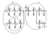
- FIGS. 1A , 1 B, and 1 Cillustrate simplified operations of a receiver switch in accordance with an example embodiment of the invention.
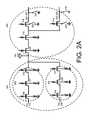
- FIGS. 2A and 2Billustrates a example CMOS switch using a multi-stacked switch at transmit (Tx) mode, in accordance with an example embodiment of the invention.
- FIG. 3illustrates an example CMOS switch using a multi-stacked switch at receive (Rx) mode, in accordance with an example embodiment of the invention.
- FIG. 4Aillustrates an example equivalent lumped model of a body floating transistor at an OFF state, according to an example embodiment of the invention.
- FIG. 4Billustrates an example equivalent lumped model of a body grounded transistor at OFF state, according to an example embodiment of the invention.
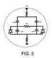
- FIG. 5illustrates a equivalent lumped model of body floating transistor at ON state.
- FIG. 6Aillustrates a multi-stacked switch at a transmit (Tx) path, in accordance with an example embodiment of the invention.
- FIG. 6Billustrates a simplified equivalent model of an OFF-state switch using body floating technique switch with signal flow, in accordance with an example embodiment of the invention.
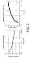
- FIG. 7illustrates example receiver switch simulation results, in accordance with an example embodiment of the invention.
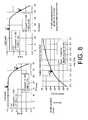
- FIG. 8illustrates example transmit switch simulation results, in accordance with an example embodiment of the invention.
- Embodiments of the inventionmay provide for CMOS RF antenna switches, which may also be referred to as SP4T CMOS switches.
- the CMOS RF antenna switches in accordance with embodiments of the inventionmay provide for one or more of multi-band operation, high power level handling, and integration with other devices and circuits.
- the CMOS RF antenna switchmay include a receiver switch and a transmit switch.
- the receiver switchmay utilize one or more switching substrate bodies, as will be described in further detail below.
- the transmit switchmay utilize a substrate body tuning technique, as will also be described in further detail below.
- FIGS. 1A-1CA CMOS RF antenna switch in accordance with an embodiment of the invention will be now be described with reference to FIGS. 1A-1C . It will be appreciated that while a particular embodiment of the CMOS RF antenna switch is illustrated in FIGS. 1A-1C , other variations of the illustrated CMOS RF antenna switch are available without departing from an embodiment of the invention.
- FIG. 1Aillustrates a simplified CMOS RF antenna switch and its operation in accordance with an example embodiment of the invention.
- the CMOS RF antenna switchmay include a transmit switch 102 and a receiver switch 104 , in accordance with an example embodiment of the invention.
- CMOS RF antenna switchmay include an antenna 100 that is in communication with at least one of the transmit switch 102 and the receiver switch 104 .
- the antenna 100may be a single multi-mode (e.g., RX and TX), multi-band antenna, although a plurality of distinct antennas may be utilized according to other embodiments of the invention.
- the receiver switch 104may be comprised of cascaded or stacked transistors 108 , 110 , 112 , and 106 , which may be Complementary Metal Oxide Semiconductor (CMOS) transistors, according to an example embodiment of the invention.
- the transistor 108may include a source 108 a , a gate 108 b , a drain 108 c , and a body substrate 108 d .
- the transistor 110may include a source 110 a , a gate 110 b , a drain 110 c , and a body substrate 110 d .
- the transistor 112may include a source 112 a , a gate 112 b , a drain 112 c , and a body substrate 112 d .
- the transistor 106may include a source 106 a , a gate 106 b , a drain 106 c , and a body substrate (not shown).
- the transistor 108may have its drain 108 c connected to the source 110 a of transistor 110 .
- the transistor 110may have its drain 110 c connected to the source of transistor 112 a .
- the drain 112 c of transistor 104may be connected to the receive (RX) block to processes received signals from the antenna 100 .
- the body substrate 112 a of the transistor 112may be connected to the source 106 a of the transistor 106 .
- the drain 106 c of the transistor 106may be connected to ground.
- at least one transistor 106which may operate as a substrate body switch for transistor 112 , may be provided at the substrate body 112 d in accordance with an example body switching technique.
- the at least one transistor 106may be switched to an ON state or an OFF state, depending on whether depending on whether a respective transmit (Tx) mode or receive (Rx) mode is in operation.
- the receiver switch 104 of FIG. 1Amay yield different equivalent circuits depending on whether the receiver switch 104 is in an OFF state, as illustrated in FIG. 1B , or an ON state, as illustrated in FIG. 1C .
- FIG. 1Billustrates an equivalent circuit of the receiver switch 104 in an OFF (e.g., disabled, block, etc.) state, according to an example embodiment of the invention.
- the receiver switch 104may be placed in the OFF state in order to provide isolation from the transmit switch 102 .
- a transmit signalmay be provided from a transmit (Tx) block to the antenna 100 .
- Txtransmit
- the stacked transistors 108 , 110 , 112may then be placed in an OFF state (e.g., opened), thereby providing a higher impedance.
- the stacked transistor 106may placed in an ON state 114 (e.g., closed), thereby shorting the substrate body 112 d of transistor 112 to ground, and reducing the signal paths for leakage current to travel from source 112 a to drain 112 c.
- ON state 114e.g., closed
- the power of the transmit (Tx) signalmay be maximized (and maximizing the power handling capability of the Tx block).
- the power handling capability of the transmit switch 102may be determined by controlling leakage current directed towards the OFF-state receiver switch 104 as well as the source-to-drain breakdown voltage of cascaded switches 108 , 110 , and 112 of the receiver switch 104 .
- the maximum transmit power of the transmit switch 102may be dependent upon the characteristics of the receiver switch 104 .
- the number of multi-stacked transistors 108 , 110 , 112may be increased to reduce the breakdown burden of each transistor 108 , 110 , 112 .
- more than three transistors 108 , 110 , and 112may be cascaded, according to another embodiment of the invention.
- the last transistor 112 from the antenna 112can control leakage current at the receiver switch 104 . If the leakage current toward OFF-state switches 108 , 110 , and 112 in the Rx path is minimized, then maximum power may be delivered from the Tx block to the antenna 100 .
- the body switching transistor 106that is connected between ground and the body substrate 112 d of transistor 112 may be used to control leakage current at the receiver switch 104 . More particularly, by placing the body switching transistor 106 in the ON state 114 , the substrate body 112 d of the last transistor 112 from the antenna 100 to the Rx block can be grounded, thereby reducing the signal paths for leakage current to travel from source 112 a to drain 112 c.
- FIG. 1Cillustrates an equivalent circuit of the receiver switch 104 in an ON (e.g., enable, receive, etc.) state, according to an example embodiment of the invention.
- the receiver switch 104may be placed in the ON position in order for the receive (RX) block to receive a signal from the antenna 100 .
- the transmit switch 102may be placed in the OFF (e.g., disabled, block) state to isolate the transmit switch 102 from the receiver switch 104 .
- the OFFe.g., disabled, block
- the stacked transistor 106when the receiver switch 104 is in an ON state, the stacked transistor 106 may be placed in an OFF state 116 , thereby providing an equivalent resistor between the body substrate 112 d of transistor 112 and ground (i.e., body floating). In this way, the insertion loss at the receive (Rx) path from the antenna 100 to the RX block may be minimized.
- FIG. 2Aillustrates an example operation of a CMOS RF antenna switch at multi-band in transmit (Tx) mode, according to an example embodiment of the invention.
- the CMOS RF antenna switch of FIG. 2Aincludes an antenna 100 in communication with a transmit switch 201 and a receiver switch 200 .
- the transmit switch 201may include a first transmit signal path Tx 1 220 that is controlled by multi-stacked transistor switches 202 and a second transmit signal path Tx 2 222 that is controlled by multi-stacked transistor switches 204 , according to an example embodiment of the invention.
- Transistor switches 202 and 204may be connected in parallel to the antenna 100 .
- Switches 202may comprise CMOS transistor switches 230 , 231 , and 232 that are cascaded or stacked from source to drain.
- the source of transistor switch 230may be connected to the drain of transistor switch 231 .
- the source of transistor switch 231may be connected to the drain of transistor switch 232 .
- switches 204may comprise CMOS transistor switches 235 , 236 , and 236 that are cascaded or stacked from source to drain.
- the source of transistor switch 235may be connected to the drain of transistor switch 236 .
- the source of transistor switch 236may be connected to the drain of transistor switch 237 .
- the receiver switch 200may include a first receive signal path Rx 1 224 and a second receive signal path Rx 2 226 that are controlled by a plurality of transistor switches, including one or more of transistor switches 208 , 210 , 212 , 205 , 206 , 214 , 209 , 210 , according to an example embodiment of the invention.
- transistor switches 208 , 2110 , 212 , 205 , 206 , 214 , 209 , 210may comprise CMOS transistor switches, according to an example embodiment of the invention.
- Switch 205may be operative to selectively connect the body substrate of transistor switch 212 between ground and a resistor, such that transistor switch 212 is either body-grounded or body-floating, according to an example embodiment of the invention.
- the switch 209may be operative to selectively connect the body substrate of transistor switch 214 between ground a resistor, such that transistor switch 214 is either body-grounded or body-floating, according to an example embodiment of the invention.
- FIG. 2Billustrates the CMOS RF antenna switch of FIG. 2A operating in a transmit (Tx) mode, according to an example embodiment of the invention. More particularly, in FIG. 2B , the CMOS RF antenna switch may be operating in transmit (Tx) mode for the first transmit (Tx) signal path Tx 1 220 .
- Txtransmit
- the stacked switches 202may be closed while the stacked switches 204 may be opened.
- stacked switches 202may be closed by placing transistor switches 230 , 231 , and 232 , respectively, in an ON state.
- stacked switches 204may be opened by placing transistor switches 235 , 236 , and 237 , respectively, in an OFF state.
- the receiver switch 200may be placed in an OFF-state, according to an example embodiment of the invention.
- at least one transistor switch 212 , 214may be body-grounded, according to an example embodiment of the invention. More specifically, transistor switches 205 and 209 may be closed (e.g., provided in ON-state 216 ) in order to short the body substrate of transistors 212 , 214 to ground, thereby providing body-grounded switches 212 , 214 . Further, transistor switches 208 , 210 , 212 , and 214 may be opened to reduce leakage current toward the receive (Rx) path, including the receive paths Rx 1 224 and Rx 2 226 .
- transistor switches 208 , 210 , 212 , and 214may be opened by placing the transistor switches in an OFF-state.
- switches 206 and 210may optionally be closed to bypass leakage signals to ground to protect the low-noise amplifier (LNA) in the receiver (Rx) block.
- LNAlow-noise amplifier
- the power handling capability of the transmit switch 201may be determined by controlling leakage current towards the OFF-state receiver switch 200 and the source-to-drain breakdown voltage of cascaded or stacked switches 208 , 210 , 212 and 214 .
- the maximum transmit power of the transmit switch 201may be dependent upon the characteristics of the receiver switch 200 .
- FIG. 2BIt will also be appreciated that variations of FIG. 2B are available without departing from embodiments of the invention.
- the second signal path Tx 2 222could have been enabled instead of the first signal path Tx 1 220 in a transmit (Tx) mode configuration without departing from embodiments of the invention.
- FIG. 4Aillustrates an equivalent lumped model of a body floating transistor at an OFF state 400 such as transistors 208 , 210 in FIG. 2B , according to an example embodiment of the invention.
- FIG. 4Billustrates an equivalent lumped model of a body grounded transistor at an OFF state 402 such as transistors 212 , 214 in FIG. 2B , according to an example embodiment of the invention.
- the equivalent models in FIGS. 4A and 4Bmay include capacitors 412 , 414 , 416 , 418 as well as p-n junction diodes 404 , 406 , according to an example embodiment of the invention.
- the voltage swingmay be divided among stacked transistors 208 , 210 , 212 , and 214 . Accordingly, the last transistors 212 , 214 may only experience only one third of the full voltage swing at the antenna 100 , thereby reducing the possibility of a source-to-drain breakdown voltage occurring for transistors 212 , 214 . It will be appreciated, however, that the voltage swing at the last transistors 212 , 214 may be different, and perhaps smaller, if additional preceding transistors are provided according to other embodiments of the invention to reduce the burden of the stacked transistors 208 , 210 , 212 , 214 .
- the transistors 208 , 210may be body floating transistors, as illustrated in FIG. 4A .
- one or both of the body switching transistors 205 , 209can be put in the ON state 216 to connect the substrate bodies of transistors 212 , 214 to ground.
- one or both of the transistors 212 , 214may be a body-grounded transistor, as illustrated in FIG. 4B , which reduces the signal paths for leakage current to travel from the source to drain of respective transistors 212 , 214 .
- the p-n junction diodes 404 , 406 of each transistor 212 , 214may turn on so that leakage current may occur by the current passing through the p-n junction diodes 404 , 406 .
- An issue with the p-n junction diodes 404 , 406 turning onmay be the possible clipping of the negative voltage swing so that power handling capability of the Tx block to the antenna 100 can be limited.
- this leakage current generated by channel formation of the OFF-state transistor 212 , 214may be prevented because the voltage level at the source of transistors 212 , 214 may be fixed by the turn on voltage of the p-n junction diode 404 .
- the multi-stacked transistors 208 , 210 , 212 , and 214 at OFF-statecan divide the voltage swing at antenna 100 port so that the last OFF-state transistors 212 , 214 , and thus, p-n junction diodes 404 , 406 , may experience only one third of voltage swing at the antenna 100 .
- the overall voltage swing at antenna 100 portmay not be sufficient to turn the p-n junction diodes 404 , 406 on at the last transistor 112 .
- FIG. 3illustrates the example operation of an RF antenna switch 200 in receive (Rx) mode, according to an example embodiment of the invention.
- both switches 202 and switch 204 of the transmit switch 201may be opened to provide antenna 100 isolation from transmit signal paths Tx 1 220 and Tx 2 222 , respectively.
- switches 220may be opened by providing transistor switches 230 , 231 , 232 in an OFF-state.
- switches 204may be opened by providing transistor switches 235 , 236 , 237 in an OFF-state, according to an example embodiment of the invention.
- switches 206 , 214may be open (e.g., provided in an OFF-state), while switches 208 , 210 , 212 may be closed (e.g., provided in an ON-state), according to an example embodiment of the invention.
- transistor switch 205(and optionally switch 209 ) may be open (e.g., provided in an OFF-state 318 ) such that the transistor switch 205 (and switch 209 ) is a body-floating transistor switch, according to an example embodiment of the invention.
- the switch 210may optionally be closed by placing it in an ON-state.
- signal path Rx 2 226 in FIG. 3could have been enabled instead of signal path Rx 1 without departing from embodiments of the invention.
- FIG. 5illustrates an equivalent lumped model of body floating transistor at ON state 500 , according to an example embodiment of the invention.
- the transistors 205 , 209may be provided in an OFF state 318 to provide body floating transistors 212 , 214 , as illustrated by the equivalent lumped model of FIG. 5 .
- the parasitic capacitors 504 , 506 , 508 , 510may provide another signal path at the ON 500 state. More specifically, the ON state 500 transistor of FIG.
- the receiver switch 200may have an ON-resistor 502 , a gate-drain capacitor 508 to gate-source capacitor 510 , and a drain-body capacitor 504 , and body-source capacitor 506 as signal paths. If the body substrate were grounded, then one of these signal paths through capacitors 504 , 506 may be lost, thereby increasing the insertion loss. Accordingly, when the receiver switch 200 is in the ON state, the last transistor 212 and/or 214 (depending on whether signal path Rx 1 224 or Rx 2 226 is utilized) may need to be in a body floating state (e.g., with transistor switch 205 , 209 in the OFF state 318 ) to ensure minimized insertion loss.
- a body floating statee.g., with transistor switch 205 , 209 in the OFF state 318
- the transmit switch structure of FIGS. 6Amay be utilized for either switch 202 for the first transmit path TX 1 220 or switch 204 for the second transmit path TX 2 222 according to an example embodiment of the invention.
- the transmit switch 600may include CMOS transistors 602 , 604 , and 606 that are cascaded or stacked from source to drain.
- the cumulative breakdown voltagecan be increased since it is split among the transistors 602 , 604 , and 606 , thereby providing for a higher power blocking capability.
- a high power blocking capabilitymay be necessary, for example, at switches 204 at the second transmit path Tx 2 222 when switches 202 at the first transmit path Tx 1 220 are closed (e.g., provided in an ON state) to transmit a signal.
- the insertion loss of the transmit switch 600may be increased, according to an embodiment of the invention.
- a body floating techniquewhich includes connecting high-value resistors 608 , 610 , and 612 at the body substrate of respective transistors 602 , 604 , 606 , may be applied to the transmit switch 102 in accordance with an embodiment of the invention. Accordingly, with the use of the resistors 608 , 610 , 612 may provide for body-floating transistors 602 , 604 , and 606 .
- the transistors 602 , 604 , and 606may use a deep N-well structure of a 0.18-um CMOS process or a similar process, which may be immune to potential latch ups due to connecting high-value resistors 608 , 610 , 612 at the body substrate of transistors 602 , 604 , 606 .
- the resistors 608 , 610 , 612which may also be referred to as body-floating resistors, may reduce the insertion loss by blocking leakage current from the substrate body to ground.
- FIG. 6Billustrates signal flow in an equivalent circuit for a single stage switch at OFF state such as transistors 602 , 604 , or 606 in FIG. 6A .
- the sizee.g., resistance value
- the parasitic capacitance valuebecomes high enough so that source-to-body parasitic capacitor 652 and drain-to-body parasitic capacitor 654 with body floating resistor 656 may be used as an additional signal path at the ON state.
- the bodyis grounded, one of signal paths in FIG. 6B is bypassed to the ground, which results in degraded insertion loss.
- FIG. 7illustrates example simulation results for the operation of an example multi-band (e.g., 900 MHz, 1.9 GHz) receiver switch in accordance with an embodiment of the invention.
- These simulation resultsillustrate the insertion loss and the isolation from the antenna 100 to the transmit paths Tx 1 and Tx 2 .
- the solid linerepresents the first band at 1.9 GHz while the circled line represents the second band at 900 MHz.
- FIG. 8illustrates example simulation results for the operation of an example multi-band transmit switch in accordance with an example embodiment of the invention.
- the simulation results in FIG. 8illustrate the power handling capability for the transmit switch for low and high bands as well as the isolation from the antenna to the receive (Rx) signal paths Rx 1 and Rx 2 .
- Table Iillustrates additional simulation results for a SP4T CMOS switch using a body switching technique in multi-stacking transistor in accordance with an embodiment of the invention.
- the simulation resultsmeet the demand of the high power handling capability at both bands (800-900 MHz and 1800-1900 MHz).
- the switched resonator provided by a receiver switch 200 at a the receive (Rx) pathin conjunction with the stacked transistors provided by the transmit switch 201 , may provide high isolation at Tx mode from the antenna 100 to Rx, which can protect receiver circuit components such as LNAs from high power Tx signals.
- isolation between Rx 1 and Rx 2may also high enough to prevent a signal from one path (e.g., Rx 2 ) from leaking to the other path (e.g., Rx 1 ).
Landscapes
- Engineering & Computer Science (AREA)
- Computer Networks & Wireless Communication (AREA)
- Signal Processing (AREA)
- Electronic Switches (AREA)
Abstract
Description
| TABLE I | |||
| Frequency | |||
| 800-900 MHz | 1800-1900 MHz | ||
| TX | IL | −1.1 | dB | −1.2 | dB | ||
| P1dB | 31.5 | dBm | 31.5 | dBm | |||
| Isolation | −55 | dB | −45 | dB | |||
| Ant to RX | |||||||
| RX | IL | −1 | dB | −1.5 | dB | ||
| Isolation | −32 | dB | −27 | dB | |||
| Rx1 to Rx2 | |||||||
| Isolation | −25 | dB | −20 | dB | |||
| Ant to TX | |||||||
Claims (18)
Priority Applications (6)
| Application Number | Priority Date | Filing Date | Title |
|---|---|---|---|
| US11/857,322US7890063B2 (en) | 2006-10-03 | 2007-09-18 | Systems, methods, and apparatuses for complementary metal oxide semiconductor (CMOS) antenna switches using body switching in multistacking structure |
| DE102007046883.2ADE102007046883B4 (en) | 2006-10-03 | 2007-09-28 | Systems, methods and devices for CMOS antenna switches using body switching in a multi-stack structure |
| CN2007101638325ACN101159440B (en) | 2006-10-03 | 2007-09-30 | Systems, methods, and apparatuses for complementary metal oxide semiconductor (cmos) antenna switches using body switching in multistacking structure |
| KR1020070099372AKR100946001B1 (en) | 2006-10-03 | 2007-10-02 | Complementary Metal Oxide Semiconductor Antenna Switch System, Method and Apparatus Using Body Switching in Multi-Stack Structure |
| GB0719303AGB2442848B (en) | 2006-10-03 | 2007-10-03 | Systems, methods and apparatuses for complementary metal oxide semiconductor (cmos) antenna switches using body switching in multi stacking structure |
| FR0758027AFR2906655B1 (en) | 2006-10-03 | 2007-10-03 | SYSTEMS, METHODS, AND APPARATUS FOR ANTENNA SWITCHES IN COMPLEMENTARY SEMICONDUCTOR OXIDE (CMOS) METAL TECHNOLOGY USING BODY SWITCHING IN A MULTIPLE STACKING STRUCTURE |
Applications Claiming Priority (2)
| Application Number | Priority Date | Filing Date | Title |
|---|---|---|---|
| US82793106P | 2006-10-03 | 2006-10-03 | |
| US11/857,322US7890063B2 (en) | 2006-10-03 | 2007-09-18 | Systems, methods, and apparatuses for complementary metal oxide semiconductor (CMOS) antenna switches using body switching in multistacking structure |
Publications (2)
| Publication Number | Publication Date |
|---|---|
| US20080079653A1 US20080079653A1 (en) | 2008-04-03 |
| US7890063B2true US7890063B2 (en) | 2011-02-15 |
Family
ID=39259201
Family Applications (1)
| Application Number | Title | Priority Date | Filing Date |
|---|---|---|---|
| US11/857,322Expired - Fee RelatedUS7890063B2 (en) | 2006-10-03 | 2007-09-18 | Systems, methods, and apparatuses for complementary metal oxide semiconductor (CMOS) antenna switches using body switching in multistacking structure |
Country Status (6)
| Country | Link |
|---|---|
| US (1) | US7890063B2 (en) |
| KR (1) | KR100946001B1 (en) |
| CN (1) | CN101159440B (en) |
| DE (1) | DE102007046883B4 (en) |
| FR (1) | FR2906655B1 (en) |
| GB (1) | GB2442848B (en) |
Cited By (25)
| Publication number | Priority date | Publication date | Assignee | Title |
|---|---|---|---|---|
| US20110187417A1 (en)* | 2010-02-01 | 2011-08-04 | Samsung Electro-Mechanics Co., Ltd. | Radio frequency switch circuit |
| US20110187475A1 (en)* | 2010-02-01 | 2011-08-04 | Samsung Electro-Mechanics Co., Ltd. | Radio frequency switch circuit |
| US20120154017A1 (en)* | 2010-12-20 | 2012-06-21 | Samsung Electro-Mechanics Co., Ltd. | High frequency switch |
| US20130023221A1 (en)* | 2011-07-19 | 2013-01-24 | Yu Sin Kim | Rf antenna switch circuit, high frequency antenna component, and mobile communication device |
| US20130187728A1 (en)* | 2012-01-20 | 2013-07-25 | Samsung Electro-Mechanics Co., Ltd. | High frequency switch |
| US8604873B2 (en) | 2010-12-05 | 2013-12-10 | Rf Micro Devices (Cayman Islands), Ltd. | Ground partitioned power amplifier for stable operation |
| US8624678B2 (en) | 2010-12-05 | 2014-01-07 | Rf Micro Devices (Cayman Islands), Ltd. | Output stage of a power amplifier having a switched-bulk biasing and adaptive biasing |
| US20140009209A1 (en)* | 2012-07-07 | 2014-01-09 | Skyworks Solutions, Inc. | Radio-frequency switch having dynamic body coupling |
| US8629725B2 (en) | 2010-12-05 | 2014-01-14 | Rf Micro Devices (Cayman Islands), Ltd. | Power amplifier having a nonlinear output capacitance equalization |
| US20140055191A1 (en)* | 2012-08-23 | 2014-02-27 | Hideep Inc | Low power rf switch |
| US8731490B2 (en) | 2012-07-27 | 2014-05-20 | Rf Micro Devices (Cayman Islands), Ltd. | Methods and circuits for detuning a filter and matching network at the output of a power amplifier |
| US8729948B2 (en)* | 2012-01-20 | 2014-05-20 | Samsung Electro-Mechanics Co., Ltd. | High frequency switch |
| US8766724B2 (en) | 2010-12-05 | 2014-07-01 | Rf Micro Devices (Cayman Islands), Ltd. | Apparatus and method for sensing and converting radio frequency to direct current |
| US8843083B2 (en) | 2012-07-09 | 2014-09-23 | Rf Micro Devices (Cayman Islands), Ltd. | CMOS switching circuitry of a transmitter module |
| US8975950B2 (en) | 2012-07-07 | 2015-03-10 | Skyworks Solutions, Inc. | Switching device having a discharge circuit for improved intermodulation distortion performance |
| US9013225B2 (en) | 2013-02-04 | 2015-04-21 | Skyworks Solutions, Inc. | RF switches having increased voltage swing uniformity |
| US9059702B2 (en) | 2012-07-07 | 2015-06-16 | Skyworks Solutions, Inc. | Switch linearization by non-linear compensation of a field-effect transistor |
| US20150180465A1 (en)* | 2013-12-20 | 2015-06-25 | Samsung Electro-Mechanics Co., Ltd. | Rf switch |
| US9124354B2 (en) | 2011-05-12 | 2015-09-01 | St-Ericsson Sa | Isolation and protection circuit for a receiver in a wireless communication device |
| US9148194B2 (en) | 2012-07-07 | 2015-09-29 | Skyworks Solutions, Inc. | Radio-frequency switch system having improved intermodulation distortion performance |
| US9160328B2 (en) | 2012-07-07 | 2015-10-13 | Skyworks Solutions, Inc. | Circuits, devices, methods and applications related to silicon-on-insulator based radio-frequency switches |
| US9276570B2 (en) | 2012-07-07 | 2016-03-01 | Skyworks Solutions, Inc. | Radio-frequency switch having gate node voltage compensation network |
| US9628075B2 (en) | 2012-07-07 | 2017-04-18 | Skyworks Solutions, Inc. | Radio-frequency switch having dynamic body coupling |
| US10147724B2 (en) | 2012-07-07 | 2018-12-04 | Skyworks Solutions, Inc. | Feed-forward circuit to improve intermodulation distortion performance of radio-frequency switch |
| US10693231B2 (en) | 2017-09-11 | 2020-06-23 | Qualcomm Incorporated | Transmit/receive switching circuit |
Families Citing this family (20)
| Publication number | Priority date | Publication date | Assignee | Title |
|---|---|---|---|---|
| US7890063B2 (en) | 2006-10-03 | 2011-02-15 | Samsung Electro-Mechanics | Systems, methods, and apparatuses for complementary metal oxide semiconductor (CMOS) antenna switches using body switching in multistacking structure |
| EP2080273B1 (en)* | 2006-11-10 | 2018-09-05 | Skyworks Solutions, Inc. | Compact low loss high frequency switch with improved linearity performance |
| US7843280B2 (en)* | 2006-12-01 | 2010-11-30 | Samsung Electro-Mechanics Company | Systems, methods, and apparatuses for high power complementary metal oxide semiconductor (CMOS) antenna switches using body switching and substrate junction diode controlling in multistacking structure |
| US7817966B2 (en)* | 2007-07-13 | 2010-10-19 | Skyworks Solutions, Inc. | Switching device with reduced intermodulation distortion |
| US7738841B2 (en)* | 2007-09-14 | 2010-06-15 | Samsung Electro-Mechanics | Systems, methods and apparatuses for high power complementary metal oxide semiconductor (CMOS) antenna switches using body switching and external component in multi-stacking structure |
| US9570974B2 (en) | 2010-02-12 | 2017-02-14 | Infineon Technologies Ag | High-frequency switching circuit |
| JP5476198B2 (en)* | 2010-04-19 | 2014-04-23 | ルネサスエレクトロニクス株式会社 | High frequency switch circuit |
| JP5714886B2 (en)* | 2010-12-20 | 2015-05-07 | サムソン エレクトロ−メカニックス カンパニーリミテッド. | High frequency switch |
| GB201102143D0 (en)* | 2011-02-08 | 2011-03-23 | Cambridge Silicon Radio Ltd | A receiver |
| CN103219976A (en)* | 2012-01-19 | 2013-07-24 | 三星电机株式会社 | High-frequency switch |
| JP5880114B2 (en)* | 2012-02-17 | 2016-03-08 | ソニー株式会社 | Integrated circuit and wireless communication device |
| US9106198B2 (en)* | 2012-08-23 | 2015-08-11 | Qualcomm Incorporated | High power tunable capacitor |
| US9590674B2 (en)* | 2012-12-14 | 2017-03-07 | Peregrine Semiconductor Corporation | Semiconductor devices with switchable ground-body connection |
| CN104852715A (en)* | 2015-04-17 | 2015-08-19 | 上海华虹宏力半导体制造有限公司 | Radio frequency antenna switch |
| CN105227167B (en)* | 2015-09-21 | 2018-09-25 | 温州大学 | A kind of cmos switch circuit |
| US10298187B2 (en)* | 2016-08-12 | 2019-05-21 | Qualcomm Incorporated | Selective high and low power amplifier switch architecture |
| CN106656127B (en)* | 2016-10-12 | 2020-09-15 | 上海华虹宏力半导体制造有限公司 | Radio frequency switch circuit |
| US9960737B1 (en) | 2017-03-06 | 2018-05-01 | Psemi Corporation | Stacked PA power control |
| CN114499484B (en)* | 2021-12-28 | 2023-04-18 | 电子科技大学 | Dual-band ultra-wideband 4 x 8 radio frequency matrix switch |
| CN118508942B (en)* | 2023-09-20 | 2025-09-05 | 荣耀终端股份有限公司 | Radio frequency switch and control method of radio frequency switch |
Citations (24)
| Publication number | Priority date | Publication date | Assignee | Title |
|---|---|---|---|---|
| WO1995008868A1 (en) | 1993-09-20 | 1995-03-30 | Micrel, Inc. | Field effect transistor with switchable body to source connection |
| US5461265A (en) | 1992-05-25 | 1995-10-24 | Matsushita Electric Industrial Co., Ltd. | High-frequency variable impedance circuit having improved linearity of operating characteristics |
| JPH08237166A (en) | 1995-02-24 | 1996-09-13 | Murata Mfg Co Ltd | Antenna multicoupler with built-in rf switch |
| US5617055A (en) | 1994-07-29 | 1997-04-01 | Sgs-Thomson Microelectronics S.R.L. | Electronic switch having reduced body effect |
| US5818099A (en) | 1996-10-03 | 1998-10-06 | International Business Machines Corporation | MOS high frequency switch circuit using a variable well bias |
| US6094088A (en) | 1997-02-26 | 2000-07-25 | Nec Corporation | Radio frequency switch circuit having resistors connected to back gates of transistors |
| US6396325B2 (en) | 1999-12-03 | 2002-05-28 | Fairchild Semiconductor Corporation | High frequency MOSFET switch |
| US20030090313A1 (en) | 2001-10-10 | 2003-05-15 | Burgener Mark L. | Switch circuit and method of switching radio frequency signals |
| US6788957B1 (en) | 1998-09-23 | 2004-09-07 | Sagem Sa | Two-band transmitter-receiver with dual radiation device |
| US20040214535A1 (en) | 2003-04-25 | 2004-10-28 | Shahla Khorram | High speed CMOS transmit-receive antenna switch |
| US6836172B2 (en) | 2002-05-30 | 2004-12-28 | Nec Compound Semiconductor Devices, Ltd. | Semiconductor switch apparatus including isolated MOS transistors |
| US6882829B2 (en)* | 2002-04-02 | 2005-04-19 | Texas Instruments Incorporated | Integrated circuit incorporating RF antenna switch and power amplifier |
| CN1689241A (en) | 2002-10-14 | 2005-10-26 | 皇家飞利浦电子股份有限公司 | Transmit and receive antenna switch |
| US20060119451A1 (en) | 2004-12-08 | 2006-06-08 | Airoha Technology Corp. | Switching circuits |
| US7092677B1 (en) | 2002-09-05 | 2006-08-15 | Analog Devices, Inc. | 2V SPDT switch for high power RF wireless applications |
| US20060194558A1 (en) | 2005-02-03 | 2006-08-31 | Kelly Dylan J | Canceling harmonics in semiconductor RF switches |
| US20060199563A1 (en) | 2005-02-09 | 2006-09-07 | Kelly Dylan J | Unpowered switch and bleeder circuit |
| US20060252394A1 (en) | 2005-04-21 | 2006-11-09 | Atsushi Suwa | Switching circuit |
| US20070049237A1 (en) | 2005-08-30 | 2007-03-01 | Toshihiro Miura | Semiconductor integrated circuit device and high frequency power amplifier module |
| US20080079653A1 (en) | 2006-10-03 | 2008-04-03 | Minsik Ahn | Systems, Methods, and Apparatuses for Complementary Metal Oxide Semiconductor (CMOS) Antenna Switches Using Body Switching in Multistacking Structure |
| US20080129642A1 (en) | 2006-12-01 | 2008-06-05 | Minsik Ahn | Systems, Methods, and Apparatuses for High Power Complementary Metal Oxide Semiconductor (CMOS) Antenna Switches Using Body Switching and Substrate Junction Diode Controlling in Multistacking Structure |
| US20080247338A1 (en) | 2005-04-08 | 2008-10-09 | Matsushita Electric Industrial Co., Ltd. | High-Frequency Amplifier, and Transmission/Reception System |
| US20100001351A1 (en) | 2006-09-21 | 2010-01-07 | Nanyang Technological University | Triple well transmit-receive switch transistor |
| US7659770B2 (en) | 2007-04-17 | 2010-02-09 | Kabushiki Kaisha Toshiba | High frequency switching circuit |
- 2007
- 2007-09-18USUS11/857,322patent/US7890063B2/ennot_activeExpired - Fee Related
- 2007-09-28DEDE102007046883.2Apatent/DE102007046883B4/ennot_activeExpired - Fee Related
- 2007-09-30CNCN2007101638325Apatent/CN101159440B/ennot_activeExpired - Fee Related
- 2007-10-02KRKR1020070099372Apatent/KR100946001B1/ennot_activeExpired - Fee Related
- 2007-10-03GBGB0719303Apatent/GB2442848B/ennot_activeExpired - Fee Related
- 2007-10-03FRFR0758027Apatent/FR2906655B1/ennot_activeExpired - Fee Related
Patent Citations (27)
| Publication number | Priority date | Publication date | Assignee | Title |
|---|---|---|---|---|
| US5461265A (en) | 1992-05-25 | 1995-10-24 | Matsushita Electric Industrial Co., Ltd. | High-frequency variable impedance circuit having improved linearity of operating characteristics |
| WO1995008868A1 (en) | 1993-09-20 | 1995-03-30 | Micrel, Inc. | Field effect transistor with switchable body to source connection |
| US5617055A (en) | 1994-07-29 | 1997-04-01 | Sgs-Thomson Microelectronics S.R.L. | Electronic switch having reduced body effect |
| JPH08237166A (en) | 1995-02-24 | 1996-09-13 | Murata Mfg Co Ltd | Antenna multicoupler with built-in rf switch |
| US5818099A (en) | 1996-10-03 | 1998-10-06 | International Business Machines Corporation | MOS high frequency switch circuit using a variable well bias |
| US6094088A (en) | 1997-02-26 | 2000-07-25 | Nec Corporation | Radio frequency switch circuit having resistors connected to back gates of transistors |
| US6788957B1 (en) | 1998-09-23 | 2004-09-07 | Sagem Sa | Two-band transmitter-receiver with dual radiation device |
| US6396325B2 (en) | 1999-12-03 | 2002-05-28 | Fairchild Semiconductor Corporation | High frequency MOSFET switch |
| US20030090313A1 (en) | 2001-10-10 | 2003-05-15 | Burgener Mark L. | Switch circuit and method of switching radio frequency signals |
| US6882829B2 (en)* | 2002-04-02 | 2005-04-19 | Texas Instruments Incorporated | Integrated circuit incorporating RF antenna switch and power amplifier |
| US6836172B2 (en) | 2002-05-30 | 2004-12-28 | Nec Compound Semiconductor Devices, Ltd. | Semiconductor switch apparatus including isolated MOS transistors |
| US7092677B1 (en) | 2002-09-05 | 2006-08-15 | Analog Devices, Inc. | 2V SPDT switch for high power RF wireless applications |
| CN1689241A (en) | 2002-10-14 | 2005-10-26 | 皇家飞利浦电子股份有限公司 | Transmit and receive antenna switch |
| US20060141943A1 (en) | 2002-10-14 | 2006-06-29 | De Graauw Antonius Johannes M | Transmit and receive antenna switch |
| US7233775B2 (en)* | 2002-10-14 | 2007-06-19 | Nxp B.V. | Transmit and receive antenna switch |
| US20040214535A1 (en) | 2003-04-25 | 2004-10-28 | Shahla Khorram | High speed CMOS transmit-receive antenna switch |
| US20060119451A1 (en) | 2004-12-08 | 2006-06-08 | Airoha Technology Corp. | Switching circuits |
| US20060194558A1 (en) | 2005-02-03 | 2006-08-31 | Kelly Dylan J | Canceling harmonics in semiconductor RF switches |
| US20060199563A1 (en) | 2005-02-09 | 2006-09-07 | Kelly Dylan J | Unpowered switch and bleeder circuit |
| US20080247338A1 (en) | 2005-04-08 | 2008-10-09 | Matsushita Electric Industrial Co., Ltd. | High-Frequency Amplifier, and Transmission/Reception System |
| US20060252394A1 (en) | 2005-04-21 | 2006-11-09 | Atsushi Suwa | Switching circuit |
| US20070049237A1 (en) | 2005-08-30 | 2007-03-01 | Toshihiro Miura | Semiconductor integrated circuit device and high frequency power amplifier module |
| US20100001351A1 (en) | 2006-09-21 | 2010-01-07 | Nanyang Technological University | Triple well transmit-receive switch transistor |
| GB2442848A (en) | 2006-10-03 | 2008-04-16 | Samsung Electro Mech | A MOS antenna transmit-receive switch with substrate switching for improved isolation |
| US20080079653A1 (en) | 2006-10-03 | 2008-04-03 | Minsik Ahn | Systems, Methods, and Apparatuses for Complementary Metal Oxide Semiconductor (CMOS) Antenna Switches Using Body Switching in Multistacking Structure |
| US20080129642A1 (en) | 2006-12-01 | 2008-06-05 | Minsik Ahn | Systems, Methods, and Apparatuses for High Power Complementary Metal Oxide Semiconductor (CMOS) Antenna Switches Using Body Switching and Substrate Junction Diode Controlling in Multistacking Structure |
| US7659770B2 (en) | 2007-04-17 | 2010-02-09 | Kabushiki Kaisha Toshiba | High frequency switching circuit |
Non-Patent Citations (22)
| Title |
|---|
| "0.13 mum CMOS SOI SP6T Antenna Switch for Multi-Standard handsets," Dig. SiRF, pp. 58-61, Jan. 2006. |
| "0.13 μm CMOS SOI SP6T Antenna Switch for Multi-Standard handsets," Dig. SiRF, pp. 58-61, Jan. 2006. |
| Amendment to UK Search Report for Application No. GB0719303.0 dated Feb. 29, 2008. |
| Combined Search and Examination Report for GB0816744.7 mailed Jan. 12, 2009. |
| Feng-Jung Huang et al. "Single-pole double-throw CMOS switches for 900-MHz and 2.4-GHz applications on p- silicon substrates", IEEE Journal of Solid-State Circuits, vol. 39, No. 1, pp. 35- 41, Jan. 2004. |
| International Search Report for GB0723464.4 dated Feb. 28, 2008. |
| Karl Goser, Grobetaintegrationstechnik - Teil 1: Vom Transistor zur Grundschaltung. Heidelberg: Hüthig, 1990, S. 99-10. ISBN: 3-7785-1615-9. |
| Karl Goser, Groβintegrationstechnik - Teil 1: Vom Transistor zur Grundschaltung. Heidelberg: Hüthig, 1990, S. 99-10. ISBN: 3-7785-1615-9. |
| Mei-Chao Yeh et al. "Design and analysis for a miniature CMOS SPDT switch using body-floating technique to improve performance", IEEE Transactions on Microwave Theory and Techniques, vol. 54 No. 1, pp. 31-39, Jan. 2006. |
| Mei-Chao Yeh, et al. "A Miniature Low-Insertion-Loss, High-Power CMOS SPDT Switch Using Floating-Body Technique for 2.4- and 5.8- GHz Applications." IEEE Xplore. May 7, 2009, p. 451-454. |
| Mei-Chao Yeh, et al., "Design and Analysis for a Miniature CMOS SPDT Switch Using Body-Floating Technique to Improve Power Performance." IEEE Transactions on Microwave Theory and Techniques, Jan. 2006: vol. 54, p. 31-39. |
| Minsik Ahn et al. "A high-power CMOS switch using a novel adaptive voltage swing distribution method in multistack FETs", IEEE Trans. on Microwave Theory and Techniques, vol. 56, No. 4, pp. 849-858, Apr. 2008. |
| Niranjan A. Talwalkar, et al. "Integrated CMOS Transmit-Receive Switch Using LC-Tuned Substrate Bias for 2.4- and 5.2-GHz Applications." IEEE Xplore. May 8, 2009, p. 863-870. |
| Notice of Allowance dated Jul. 27, 2010 for U.S. Appl. No. 11/943,378. |
| Notice of Allowance dated Mar. 10, 2010 for Application No. 11/855,950. |
| Office Action dated Jan. 15, 2010 for German Patent Application No. 102007057656.2. |
| Office Action dated Jan. 19, 2010 for German Patent Application No. 102008046778.2. |
| Office Action dated Nov. 11, 2008 for German Patent Application No. 102007046883.2. |
| Office Action for Chinese Patent Application No. 200710163832.5 dated May 11, 2010. |
| Office Action mailed on Jul. 23, 2009 for Korean Patent Application No. 10-2007-0099372. |
| United Kingdom International Search Report for GB0710606.5, dated Sep. 27, 2007. |
| United Kingdom International Search Report for GB0719303.0 dated Jan. 24, 2008. |
Cited By (40)
| Publication number | Priority date | Publication date | Assignee | Title |
|---|---|---|---|---|
| US8461919B2 (en)* | 2010-02-01 | 2013-06-11 | Samsung Electro-Mechanics Co., Ltd | Radio frequency switch circuit |
| US20110187475A1 (en)* | 2010-02-01 | 2011-08-04 | Samsung Electro-Mechanics Co., Ltd. | Radio frequency switch circuit |
| US20110187417A1 (en)* | 2010-02-01 | 2011-08-04 | Samsung Electro-Mechanics Co., Ltd. | Radio frequency switch circuit |
| US8476959B2 (en)* | 2010-02-01 | 2013-07-02 | Samsung Electro-Mechanics Co., Ltd. | Radio frequency switch circuit |
| US8624678B2 (en) | 2010-12-05 | 2014-01-07 | Rf Micro Devices (Cayman Islands), Ltd. | Output stage of a power amplifier having a switched-bulk biasing and adaptive biasing |
| US8629725B2 (en) | 2010-12-05 | 2014-01-14 | Rf Micro Devices (Cayman Islands), Ltd. | Power amplifier having a nonlinear output capacitance equalization |
| US8604873B2 (en) | 2010-12-05 | 2013-12-10 | Rf Micro Devices (Cayman Islands), Ltd. | Ground partitioned power amplifier for stable operation |
| US8766724B2 (en) | 2010-12-05 | 2014-07-01 | Rf Micro Devices (Cayman Islands), Ltd. | Apparatus and method for sensing and converting radio frequency to direct current |
| US8779840B2 (en)* | 2010-12-20 | 2014-07-15 | Samsung Electro-Mechanics Co., Ltd. | High frequency switch |
| US20120154017A1 (en)* | 2010-12-20 | 2012-06-21 | Samsung Electro-Mechanics Co., Ltd. | High frequency switch |
| US9124354B2 (en) | 2011-05-12 | 2015-09-01 | St-Ericsson Sa | Isolation and protection circuit for a receiver in a wireless communication device |
| US20130023221A1 (en)* | 2011-07-19 | 2013-01-24 | Yu Sin Kim | Rf antenna switch circuit, high frequency antenna component, and mobile communication device |
| US8909171B2 (en)* | 2011-07-19 | 2014-12-09 | Samsung Electro-Mechanics Co., Ltd. | RF antenna switch circuit, high frequency antenna component, and mobile communication device |
| US9065164B2 (en)* | 2012-01-20 | 2015-06-23 | Samsung Electro-Mechanics Co., Ltd. | High frequency switch |
| US8729948B2 (en)* | 2012-01-20 | 2014-05-20 | Samsung Electro-Mechanics Co., Ltd. | High frequency switch |
| US20130187728A1 (en)* | 2012-01-20 | 2013-07-25 | Samsung Electro-Mechanics Co., Ltd. | High frequency switch |
| US20140218126A1 (en)* | 2012-01-20 | 2014-08-07 | Samsung Electro-Mechanics Co., Ltd. | High frequency switch |
| US9035716B2 (en)* | 2012-01-20 | 2015-05-19 | Samsung Electro-Mechanics Co., Ltd. | High frequency switch |
| US9450579B2 (en) | 2012-07-07 | 2016-09-20 | Skyworks Solutions, Inc. | Radio frequency devices having reduced intermodulation distortion |
| US9628075B2 (en) | 2012-07-07 | 2017-04-18 | Skyworks Solutions, Inc. | Radio-frequency switch having dynamic body coupling |
| US10147724B2 (en) | 2012-07-07 | 2018-12-04 | Skyworks Solutions, Inc. | Feed-forward circuit to improve intermodulation distortion performance of radio-frequency switch |
| US9973184B2 (en) | 2012-07-07 | 2018-05-15 | Skyworks Solutions, Inc. | Radio-frequency devices with gate node voltage compensation |
| US9059702B2 (en) | 2012-07-07 | 2015-06-16 | Skyworks Solutions, Inc. | Switch linearization by non-linear compensation of a field-effect transistor |
| US9685943B2 (en) | 2012-07-07 | 2017-06-20 | Skyworks Solutions, Inc. | Switching device having a discharge circuit for improved intermodulation distortion performance |
| US8975950B2 (en) | 2012-07-07 | 2015-03-10 | Skyworks Solutions, Inc. | Switching device having a discharge circuit for improved intermodulation distortion performance |
| US9595951B2 (en) | 2012-07-07 | 2017-03-14 | Skyworks Solutions, Inc. | Radio-frequency switches having gate bias and frequency-tuned body bias |
| US9148194B2 (en) | 2012-07-07 | 2015-09-29 | Skyworks Solutions, Inc. | Radio-frequency switch system having improved intermodulation distortion performance |
| US9160328B2 (en) | 2012-07-07 | 2015-10-13 | Skyworks Solutions, Inc. | Circuits, devices, methods and applications related to silicon-on-insulator based radio-frequency switches |
| US9276570B2 (en) | 2012-07-07 | 2016-03-01 | Skyworks Solutions, Inc. | Radio-frequency switch having gate node voltage compensation network |
| US9294083B2 (en) | 2012-07-07 | 2016-03-22 | Skyworks Solutions, Inc. | Semiconductor devices and methods providing non-linear compensation of field-effect transistors |
| US20140009209A1 (en)* | 2012-07-07 | 2014-01-09 | Skyworks Solutions, Inc. | Radio-frequency switch having dynamic body coupling |
| US9590614B2 (en) | 2012-07-07 | 2017-03-07 | Skyworks Solutions, Inc. | Non-linearity compensation in radio frequency switches and devices |
| US8843083B2 (en) | 2012-07-09 | 2014-09-23 | Rf Micro Devices (Cayman Islands), Ltd. | CMOS switching circuitry of a transmitter module |
| US8731490B2 (en) | 2012-07-27 | 2014-05-20 | Rf Micro Devices (Cayman Islands), Ltd. | Methods and circuits for detuning a filter and matching network at the output of a power amplifier |
| US20140055191A1 (en)* | 2012-08-23 | 2014-02-27 | Hideep Inc | Low power rf switch |
| US9509363B2 (en) | 2013-02-04 | 2016-11-29 | Skyworks Solutions, Inc. | Circuits having switches providing increased voltage swing uniformity |
| US9013225B2 (en) | 2013-02-04 | 2015-04-21 | Skyworks Solutions, Inc. | RF switches having increased voltage swing uniformity |
| US20150180465A1 (en)* | 2013-12-20 | 2015-06-25 | Samsung Electro-Mechanics Co., Ltd. | Rf switch |
| US10693231B2 (en) | 2017-09-11 | 2020-06-23 | Qualcomm Incorporated | Transmit/receive switching circuit |
| US10910714B2 (en) | 2017-09-11 | 2021-02-02 | Qualcomm Incorporated | Configurable power combiner and splitter |
Also Published As
| Publication number | Publication date |
|---|---|
| DE102007046883A1 (en) | 2008-07-31 |
| GB2442848B (en) | 2011-09-07 |
| DE102007046883B4 (en) | 2017-04-27 |
| US20080079653A1 (en) | 2008-04-03 |
| CN101159440A (en) | 2008-04-09 |
| GB0719303D0 (en) | 2007-11-14 |
| FR2906655B1 (en) | 2012-06-15 |
| KR100946001B1 (en) | 2010-03-09 |
| KR20080031133A (en) | 2008-04-08 |
| GB2442848A (en) | 2008-04-16 |
| CN101159440B (en) | 2011-12-21 |
| FR2906655A1 (en) | 2008-04-04 |
Similar Documents
| Publication | Publication Date | Title |
|---|---|---|
| US7890063B2 (en) | Systems, methods, and apparatuses for complementary metal oxide semiconductor (CMOS) antenna switches using body switching in multistacking structure | |
| US7843280B2 (en) | Systems, methods, and apparatuses for high power complementary metal oxide semiconductor (CMOS) antenna switches using body switching and substrate junction diode controlling in multistacking structure | |
| US7738841B2 (en) | Systems, methods and apparatuses for high power complementary metal oxide semiconductor (CMOS) antenna switches using body switching and external component in multi-stacking structure | |
| US8165535B2 (en) | Systems, methods and apparatuses for complementary metal oxide semiconductor (CMOS) antenna switches using switched resonators | |
| US10153803B2 (en) | Receiving circuit, wireless communication module, and wireless communication device | |
| US9680463B2 (en) | System and method for a radio frequency switch | |
| US8676132B2 (en) | Semiconductor integrated circuit, RF module using the same, and radio communication terminal device using the same | |
| US10056935B2 (en) | Switching circuits for wireless applications | |
| US9948348B2 (en) | High isolation switch with notch filter | |
| KR101850769B1 (en) | Switch module, front-end module, and driving method for switch module | |
| US10778211B2 (en) | Switching circuit and semiconductor module | |
| US11336243B2 (en) | RFFE LNA topology supporting both noncontiguous intraband carrier aggregation and interband carrier aggregation | |
| KR20150034767A (en) | Circuits, devices, methods and combinations related to silicon-on-insulator based radio-frequency switches | |
| US10511344B1 (en) | Transceiver resonant receive switch | |
| US20240195368A1 (en) | Rf front-end chip, rf switch module, and rf communication device | |
| Ahn et al. | A high power CMOS SP4T switch using a switched resonator for dual band applications |
Legal Events
| Date | Code | Title | Description |
|---|---|---|---|
| AS | Assignment | Owner name:SAMSUNG ELECTRO-MECHANICS, KOREA, REPUBLIC OF Free format text:ASSIGNMENT OF ASSIGNORS INTEREST;ASSIGNORS:LEE, CHANG-HO;CHANG, JAEJOON;WOO, WANGMYONG;AND OTHERS;REEL/FRAME:020020/0713;SIGNING DATES FROM 20070920 TO 20071010 Owner name:GEORGIA TECH RESEARCH CORPORATION, GEORGIA Free format text:ASSIGNMENT OF ASSIGNORS INTEREST;ASSIGNORS:LEE, CHANG-HO;CHANG, JAEJOON;WOO, WANGMYONG;AND OTHERS;REEL/FRAME:020020/0713;SIGNING DATES FROM 20070920 TO 20071010 Owner name:SAMSUNG ELECTRO-MECHANICS, KOREA, REPUBLIC OF Free format text:ASSIGNMENT OF ASSIGNORS INTEREST;ASSIGNORS:LEE, CHANG-HO;CHANG, JAEJOON;WOO, WANGMYONG;AND OTHERS;SIGNING DATES FROM 20070920 TO 20071010;REEL/FRAME:020020/0713 Owner name:GEORGIA TECH RESEARCH CORPORATION, GEORGIA Free format text:ASSIGNMENT OF ASSIGNORS INTEREST;ASSIGNORS:LEE, CHANG-HO;CHANG, JAEJOON;WOO, WANGMYONG;AND OTHERS;SIGNING DATES FROM 20070920 TO 20071010;REEL/FRAME:020020/0713 | |
| STCF | Information on status: patent grant | Free format text:PATENTED CASE | |
| FEPP | Fee payment procedure | Free format text:PAYOR NUMBER ASSIGNED (ORIGINAL EVENT CODE: ASPN); ENTITY STATUS OF PATENT OWNER: LARGE ENTITY | |
| FPAY | Fee payment | Year of fee payment:4 | |
| MAFP | Maintenance fee payment | Free format text:PAYMENT OF MAINTENANCE FEE, 8TH YEAR, LARGE ENTITY (ORIGINAL EVENT CODE: M1552) Year of fee payment:8 | |
| FEPP | Fee payment procedure | Free format text:MAINTENANCE FEE REMINDER MAILED (ORIGINAL EVENT CODE: REM.); ENTITY STATUS OF PATENT OWNER: LARGE ENTITY | |
| LAPS | Lapse for failure to pay maintenance fees | Free format text:PATENT EXPIRED FOR FAILURE TO PAY MAINTENANCE FEES (ORIGINAL EVENT CODE: EXP.); ENTITY STATUS OF PATENT OWNER: LARGE ENTITY | |
| STCH | Information on status: patent discontinuation | Free format text:PATENT EXPIRED DUE TO NONPAYMENT OF MAINTENANCE FEES UNDER 37 CFR 1.362 | |
| FP | Lapsed due to failure to pay maintenance fee | Effective date:20230215 |