US7888959B2 - Apparatus and method for hardening latches in SOI CMOS devices - Google Patents
Apparatus and method for hardening latches in SOI CMOS devicesDownload PDFInfo
- Publication number
- US7888959B2 US7888959B2US11/857,596US85759607AUS7888959B2US 7888959 B2US7888959 B2US 7888959B2US 85759607 AUS85759607 AUS 85759607AUS 7888959 B2US7888959 B2US 7888959B2
- Authority
- US
- United States
- Prior art keywords
- transistor
- series
- latch
- fets
- hardening
- Prior art date
- Legal status (The legal status is an assumption and is not a legal conclusion. Google has not performed a legal analysis and makes no representation as to the accuracy of the status listed.)
- Expired - Fee Related, expires
Links
- 238000000034methodMethods0.000titleclaimsabstractdescription36
- 238000013461designMethods0.000description18
- 239000002245particleSubstances0.000description15
- 210000000746body regionAnatomy0.000description8
- 230000008901benefitEffects0.000description5
- 239000004065semiconductorSubstances0.000description5
- 239000000463materialSubstances0.000description4
- 238000005516engineering processMethods0.000description3
- 239000012212insulatorSubstances0.000description3
- 230000003068static effectEffects0.000description3
- 229910000577Silicon-germaniumInorganic materials0.000description2
- LEVVHYCKPQWKOP-UHFFFAOYSA-N[Si].[Ge]Chemical compound[Si].[Ge]LEVVHYCKPQWKOP-UHFFFAOYSA-N0.000description2
- 229910045601alloyInorganic materials0.000description2
- 239000000956alloySubstances0.000description2
- 239000000470constituentSubstances0.000description2
- 230000000694effectsEffects0.000description2
- 229910052732germaniumInorganic materials0.000description2
- GNPVGFCGXDBREM-UHFFFAOYSA-Ngermanium atomChemical compound[Ge]GNPVGFCGXDBREM-UHFFFAOYSA-N0.000description2
- 239000012535impuritySubstances0.000description2
- 238000011160researchMethods0.000description2
- 229910052710siliconInorganic materials0.000description2
- 239000010703siliconSubstances0.000description2
- 230000001052transient effectEffects0.000description2
- 108091006149Electron carriersProteins0.000description1
- 101100484930Saccharomyces cerevisiae (strain ATCC 204508 / S288c) VPS41 geneProteins0.000description1
- 230000005540biological transmissionEffects0.000description1
- JJWKPURADFRFRB-UHFFFAOYSA-Ncarbonyl sulfideChemical compoundO=C=SJJWKPURADFRFRB-UHFFFAOYSA-N0.000description1
- 230000000295complement effectEffects0.000description1
- 238000012937correctionMethods0.000description1
- 230000008878couplingEffects0.000description1
- 238000010168coupling processMethods0.000description1
- 238000005859coupling reactionMethods0.000description1
- 230000007547defectEffects0.000description1
- 230000007123defenseEffects0.000description1
- 230000002950deficientEffects0.000description1
- 238000011161developmentMethods0.000description1
- 230000005669field effectEffects0.000description1
- 239000007943implantSubstances0.000description1
- 238000004519manufacturing processMethods0.000description1
- 239000005022packaging materialSubstances0.000description1
- 230000005855radiationEffects0.000description1
- 238000000926separation methodMethods0.000description1
Images


Classifications
- H—ELECTRICITY
- H03—ELECTRONIC CIRCUITRY
- H03K—PULSE TECHNIQUE
- H03K3/00—Circuits for generating electric pulses; Monostable, bistable or multistable circuits
- H03K3/02—Generators characterised by the type of circuit or by the means used for producing pulses
- H03K3/353—Generators characterised by the type of circuit or by the means used for producing pulses by the use, as active elements, of field-effect transistors with internal or external positive feedback
- H03K3/356—Bistable circuits
- H03K3/356104—Bistable circuits using complementary field-effect transistors
- H03K3/356113—Bistable circuits using complementary field-effect transistors using additional transistors in the input circuit
- H03K3/356147—Bistable circuits using complementary field-effect transistors using additional transistors in the input circuit using pass gates
- H03K3/356156—Bistable circuits using complementary field-effect transistors using additional transistors in the input circuit using pass gates with synchronous operation
- H—ELECTRICITY
- H03—ELECTRONIC CIRCUITRY
- H03K—PULSE TECHNIQUE
- H03K3/00—Circuits for generating electric pulses; Monostable, bistable or multistable circuits
- H03K3/02—Generators characterised by the type of circuit or by the means used for producing pulses
- H03K3/027—Generators characterised by the type of circuit or by the means used for producing pulses by the use of logic circuits, with internal or external positive feedback
- H03K3/037—Bistable circuits
- H03K3/0375—Bistable circuits provided with means for increasing reliability; for protection; for ensuring a predetermined initial state when the supply voltage has been applied; for storing the actual state when the supply voltage fails
Definitions
- the disclosurerelates generally to transistor devices and, more specifically, to a method and apparatus for hardening latches.
- CMOSComplementary Metal-Oxide-Semiconductor circuits are susceptible to high-energy particles.
- CMOS devicesuch as an Silicon-On-Insulator (SOI) transistor
- SOISilicon-On-Insulator
- the high-energy particlecan generate a large number of electron-hole pairs, causing a large transient current to flow between the source and the drain.
- This large transient currentcauses a device, which is biased in the OFF (or non-conducting state) to become momentarily conducting, and this conduction can momentary turn the transistor ON, which can cause an error to occur in the CMOS circuit.
- SEUSingle-Event Upset
- FIG. 1illustrates a conventional latch 100 .
- the logic states of “clock” and “clock_not”are opposite of each other.
- FETsField Effect Transistors
- the latch 100is written such that “true” ⁇ “data.”
- FETs 101 , 102are OFF while FETs 104 , 105 are ON.
- the latch 100maintains its state via a pair of cross-coupled inverters formed by FETs 107 , 108 and FETs 103 , 106 .
- Embodiments of the inventionprovide a novel and non-obvious method and configuration for reducing SEU.
- the method of determining one or more transistors within a particular circuit to be respectively replaced with a hardened transistorincludes: identifying, as not requiring hardening, one or more transistors; identifying, as candidates for hardening, each transistor in the circuit not previously identified as not requiring hardening; and employing the hardened transistor in place of a transistor identified as a candidate for hardening.
- the circuitis a latch and the transistor is an SOI CMOS FET.
- the hardened transistorincludes first and second series-connected transistors having a shared source/drain region whereby a drain of the first series-connected transistor is merged with a source of the second series-connected transistor. In certain instances, hardened, series transistors are employed for all of the candidates for hardening.
- a method of determining one or more transistors within a particular latch to be respectively replaced with a hardened, series transistoridentifies each storage node; identifies, as not requiring hardening, each transistor having only a gate terminal connected to a storage node of the latch; and identifies, as not requiring hardening, each transistor that remains ON upon both of (i) the latch holding its state, and a respective storage node at logic state 0 , and (ii) the latch holding its state, and the respective storage node at logic state 1 .
- Each transistor not previously identified as not requiring hardeningare then identified as a candidate for hardening.
- a hardened, series transistoris employed in place of a transistor identified as a candidate for hardening.
- the candidates for hardeningonly include transistors being part of a cross-coupled inverter of the latch.
- the threshold voltage of the hardened transistormay be lower than a threshold voltage of a transistor being replaced by the hardened transistor.
- a circuitin yet another embodiment of the invention, includes at least one hardened, series transistor, and at least one non-hardened transistor.
- the circuitis a latch, and the at least one non-hardened transistor includes one or more transistors having only a gate terminal connected to a storage node of the latch.
- the at least one non-hardened transistorincludes one or more transistors that remain ON upon both of (i) the latch holding its state, and a respective storage node at logic state 0 , and (ii) the latch holding its state, and the respective storage node at logic state 1 .
- the candidates for hardeningmay also only include transistors that are part of a cross-coupled inverter of the latch.
- the circuitmay further include a multiplexer circuit, and the at least one non-hardened transistor includes a transistor in the latch that is directly connected to a data node, which is directly connected to the multiplexer circuit.
- the at least one non-hardened transistorincludes a transistor always driven ON during a default state of the latch.
- a hardened, series transistormay be located in all SEU-susceptible transistor nodes of the circuit.
- the circuitmay include a master latch and a slave latch, and the at least one non-hardened transistor includes a transistor in the slave latch that is directly connected to a data node, which is directly connected to the master latch.
- the transistormay be an SOI device, and the hardened, series transistor includes first and second series-connected transistors having a shared source/drain region whereby a drain of the first series-connected transistor is merged with a source of the second series-connected transistor.
- FIG. 1is a typical conventional latch
- FIG. 2illustrates a conventional FET being replaced by a SEU-hardened, series FET in accordance with the inventive arrangements
- FIGS. 3A , 3 Bare cross-sectional views, respectively, of two embodiments of a series FET in accordance with the inventive arrangements;
- FIG. 4illustrates SEU-susceptible FETs in the latch of FIG. 1 ;
- FIG. 5illustrates a SEU-hardened latch, in accordance with the inventive arrangements, in which only the cross-coupled inverters have been SEU-hardened;
- FIG. 6illustrates another SEU-hardened latch, in accordance with the inventive arrangements, in which write transistors of the latch have been SEU-hardened via the use of a hold multiplexer;
- FIG. 7illustrates a master-slave SEU-hardened latch in accordance with the inventive arrangements
- FIG. 8illustrates yet another SEU-hardened latch in which both the cross-coupled inverters and write FETs have been SEU-hardened in accordance with the inventive arrangements
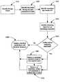
- FIG. 10is a flow chart illustrating a method of selecting transistors within a particular circuit to be replaced with SEU-hardened, series FETs in accordance with the inventive arrangements.
- nFET 201includes a gate terminal 210 , drain terminal 211 , and source terminal 212 . To SEU-harden this FET, the nFET 201 is replaced by two series-connected nFETs 202 , 203 , collectively referred to as series nFET 200 . Although described with regard to an nFET, one skilled in the art would recognize that a similar replacement can be performed using a pFET.
- the two nFETs 202 , 203are connected in series such that the drain terminal of the first nFET 203 is connected to the source terminal of the second nFET 202 at node 216 . Also, the respective gate terminals of the two nFETs are connected together at node 213 .
- the series nFET 200is used in the original circuit in place of nFET 201 .
- node 213 of the series nFET 200connects where node 210 was
- node 214i.e., the drain terminal of nFET 202
- node 215i.e., the source terminal of nFET 203
- hardened, series transistorrefers to at least two transistors having a shared gate terminal (either physically shared or in which the gate terminals of the transistors are directly, electrically connected) and in which a source of first one of the transistors is shared within a drain of a second one of the transistors (either physically shared or in which the drain is directly, electrically connected to the source).
- Other terms used herein that also refer to this structureincludes “SEU-hardened, series transistors,” “hardened FET,” and “series FET.”
- non-series transistor(and variations thereof) refers to a transistor that is not a hardened, series transistor, as defined above, or part of a series transistor.
- both nFETs 202 , 203are OFF.
- the conduction pathi.e., from source 215 to drain 214
- the second transistore.g., nFET 203
- I onis the drain to source current (I ds ) that flows upon a gate to source voltage (V gs ) being greater than the threshold voltage (V t ).
- V gsgate to source voltage
- V tthreshold voltage
- I onis the drain to source current (I ds ) that flows when a gate to source voltage (V gs ) is less then the threshold voltage (V t ).
- V tthe threshold voltage
- a lower I offtranslates to a lower standby power of an OFF transistor.
- I offmay be higher with both a higher V gs and a higher V ds .
- a lower V dsalso reduces I off .
- a designerhas the option to replace regular-V t FETs with low-V t FETs. This configuration can still meet the original power leakage requirements of a single FET 201 .
- the switching speed of the series FET 200 at a low V twill be faster than the switching speed of the series FET 200 at a regular V t .
- a designercan reduce the sizes of the low-V t series FETs versus. the sizes of the series FETs having a regular V t .
- a smaller low-V t series FETswill still have a similar I on as a larger, regular-V t series FET, but the smaller low-V t series FETs will have a smaller footprint. It should be noted, however, that reducing the V t of the FETs 202 , 203 connected in series in comparison to V t of original single FET 201 is not required.
- FETs 202 , 203have the same design and/or the same transistor parameters.
- the FET 200is not limited in this manner, as the FETs 202 , 203 may have different designs and/or transistor parameters.
- FETs 202 , 203may have the same design, the same gate insulator thickness, the same channel length or drain-to-source distance, the same p-type body region thickness and doping profile, and the same drain region doping profile.
- FETs 202 , 203may have different designs, with FETs 202 , 203 having different channel lengths, different p-type body region thicknesses and doping profiles, and/or different drain region doping profiles.
- the body region of FET 202can be either electrically shorted to its source region or not electrically shorted to its source region.
- the body region of FET 203can either be electrically shorted to its source region or not electrically shorted to its source region.
- the body regions of FETs 202 and 203can either be partially depleted (i.e., having a finite quasi-neutral body region) or fully depleted (i.e., having no quasi-neutral body region).
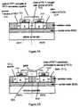
- FIGS. 3A and 3Brespectively illustrate two different configurations of the SEU-hardened, series FET.
- one configurationincludes two separate FETs 302 , 305 .
- the common node 216 illustrated in FIG. 2is formed upon the drain terminal 303 of FET 1 being connected to the source terminal 304 of FET 2 via an external connection.
- another configurationincludes two joined FETs 311 , 313 .
- the common node 216 illustrated in FIG. 2is merged into one shared structure 312 , in which the drain of FET 1 is merged with the source of FET 2 .
- the configuration of FIG. 3Ais particularly effective in devices having source/drain implants that reach all the way to a buried oxide (BOX).
- An example of a particular technology employing this configurationis Silicon-On-Insulator (SOI).
- SOISilicon-On-Insulator
- the bodies of the two FETs 311 , 313are isolated from one other.
- the majority hole or electron carriers, which are generated after a high energy particle hits the transistor body of one of the constituent SOI FETscannot flow to the transistor body of the other constituent SOI FET in the series.
- a separation distance between the two FETs 311 , 313is not required.
- the configuration employed in FIG. 3Ais employed since, for example, this configuration reduces the area overhead of the series FET.
- the most commonly used semiconductor material for forming SOIis silicon. However, any semiconductor material that is compatible with an SOI structure is acceptable for use with the present series FET. Other possible semiconductors materials include germanium, silicon-germanium alloy, and semiconductor materials that can be grown on top of silicon, such as germanium or silicon-germanium alloy.
- the present series transistorhas been described herein with reference to SOI CMOS technology, the SEU-hardened series transistor is not limited in this manner. Any transistor having either a current design or a future design with a structure upon which a high-energy particle hitting the transistor turns an OFF state into an ON state is acceptable for use with the techniques described herein.
- a Fin-FETis a FET configuration that can benefit from the teachings described herein.
- the described methods and apparatusmay be employed to reduce the effects of SEU, the described methods and apparatus are not limited in this manner. These techniques may be employed to reduce the effect of any phenomenon that is capable of causing an OFF transistor to momentarily turn ON, for example, noise coupling. Additionally, these techniques may be employed to protect latches against certain types of hard defects (created, for example, during manufacturing) which cause a single transistor to always be in an ON state (e.g., a source-drain short). In such a circumstance, the defective transistor acts as a simple conductive line and the other transistor in the series transistor group will acts solely as the switch.
- replacing each non-series FET within a particular circuit design with a series FETis not practicable or desirable.
- the overall designincurs overhead with regard to area, delay, and power consumption.
- the designgets larger from area point of view.
- the delay of two series FETsis slower then a single FET.
- clock and “data” signalsdrive twice as much capacitance, which increases the power consumption of the circuit.
- a methodcan be employed to select certain transistors within a particular circuit to be replaced with SEU-hardened, series transistors. In so doing, the overhead with regard to area, delay, and power consumption can be reduced.
- an SEU-susceptible transistoris a particular transistor, which if not hardened, would be SEU-susceptible.
- the storage nodes of a latchwhich requires hardening against SEU, are identified. Circuit designers skilled in art of latch design know what nodes in the latch are used to store data. For example, in dynamic latches, one such storage node typically exists per latch. In static latches, two such storage nodes exist per latch. FIG.
- FIG. 1illustrates a typical static latch, and nodes “true” and “comp” are the two nodes used to store data.
- the method and apparatus described hereinare in relation to the latch illustrated in FIG. 1 , the described method and apparatus are not limited in this manner. As recognized by those skilled in the art, many different types of latch/configurations, both yet to be designed and currently existing, can benefit from the methods and apparatus described herein.
- transistors that have only a gate terminal connection to either of these storage nodesare identified. These gate-connected transistors cannot be the cause of SEU, and thus, those transistors that have only a gate terminal connection to either of the storage nodes can be excluded as a candidate for hardening using the series FET.
- transistors 109 , 110each have only a gate terminal connection to a storage node, (i.e., “true”). Thus, transistors 109 , 110 do not require hardening using the series FET.
- a third stepis to analyze the remaining transistors under the condition of (1) latch holding its state and storage node at logic state 0 and (2) latch holding its state and storage node at logic state 1 .
- Any FET which remains ON for both conditions (1) and (2)is not susceptible to SEU.
- FETs 104 , 105meet both of the above-identified conditions. Thus, FETs 104 , 105 do not require hardening using the series FET.
- steps 1-3are applied to a device to be analyzed (e.g., the latch 100 of FIG. 1 ) and those FETs that do not have to be hardened are identified, the FETs that remain are the FETs that are susceptible to SEU and are identified as candidates for hardening.
- a device to be analyzede.g., the latch 100 of FIG. 1
- the FETs that remainare the FETs that are susceptible to SEU and are identified as candidates for hardening.
- FIG. 4out of the ten FETs illustrated in FIG. 1 , there are six FETs that are candidates to be replaced with the series transistors.
- step 1040a designer decides which FETs of the SEU-susceptible FETs are to be replaced by the series FETs. As already described, each time a single FET is replaced by a series FET, the design incurs overhead in terms of area, delay, and power.
- step 1080the designer may choose to harden all of the SEU-susceptible FETs. For example, referring to FIG. 4 , a designer may choose to harden all six transistors.
- FIG. 8illustrates a configuration in which all six transistors identified in FIG. 4 as being SEU-susceptible are converted into series FETs.
- step 1050the designer may make a determination that by replacing only a subset of SEU-susceptible FETs, the failure rate of a given latch resulting from SEU will be reduced below an acceptable level.
- the amount of overhead incurred to the design, in terms of area, delay, and/or powermay be reduced.
- steps 1060 and 1070certain possible selection techniques for selecting a subset of SEU-susceptible FETs are described below as steps 1060 and 1070 . Despite the description of steps 1060 and 1070 being separately performed, the method is not limited in this manner. For example, steps 1060 and 1070 (and/or other selection techniques) can be performed together to select the subset of SEU-susceptible FETs to be replaced.
- one selection technique for identifying a subset of SEU-susceptible FETs to be replacedis to only select FETs that are part of a cross-coupled inverter (e.g., 403 / 406 and 407 / 408 of FIG. 4 ).
- An advantage of this techniqueis that clock nets “clock” and “clock_not” still drive a single FET. Since AC power from clock nets is one of the major consumers of power, the implementation illustrated in FIG. 5 does not increase required clock power. Additionally, with the latch of FIG.
- the critical latch delayis from node “data” through the transmission gate formed by FETs 501 / 502 to node “true,” and from node “true” through the inverter formed by FETs 509 / 510 to latch output node “latch_not.”
- the series FETsare slower then the single FET being replaced.
- the resultant configuration in FIG. 5does not place any series FETs in this delay-critical path, and thus, the latch delay does not increase.
- FIG. 6only conceptually illustrates how the latch may be hardened. As recognized by those skilled in the art of circuit design, many different ways exist to implement the techniques described herein with other circuit elements.
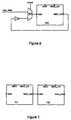
- FIG. 7illustrates another technique for protecting, from SEU, write transistors in a latch that only has hardened cross-coupled inverters.
- This techniqueinvolves using a master 701 -slave 702 configuration.
- the master latchholds the same data as the slave latch.
- the slave latchmay then be hardened (e.g., using the configuration illustrated in FIG. 5 ). In so doing, even if high energy particle hits FETs 501 or 502 (see FIG. 5 ) in the slave latch, the slave latch will be re-written with the correct data from the master latch.
- the FETs 501 , 502 of FIG. 5are not required to be hardened.
- step 1070certain transistors are removed as candidates for hardening because they are always ON. For example, if “true” has a very high probability of being 0, then pFET 9071 has a very high probability of being ON.
- the nFET 9060also has a very high probability on being ON. In this situation, the cost/benefit ratio of hardening FETs 9071 , 9060 may be too high; and thus, these FETs may be removed as candidates for hardening. In so doing, the area, power, delay overhead for the latch can be reduced.
- a determinationmay be made as to the likelihood that the node “data” is opposite the node “true.” If the determination yields a low likelihood that the node “data” is opposite the node “true,” then the likelihood is also low that even if FETs 901 or 902 were turned ON, then the latch would be written to the incorrect state. In this situation, the cost/benefit ratio of hardening FETs 901 , 902 may also be too high; and thus, these FETs may also be removed as candidates for hardening. This circumstance may occur, for example, in static circuits in which data switches very infrequently.
Landscapes
- Semiconductor Integrated Circuits (AREA)
- Metal-Oxide And Bipolar Metal-Oxide Semiconductor Integrated Circuits (AREA)
- Design And Manufacture Of Integrated Circuits (AREA)
Abstract
Description
Claims (4)
Priority Applications (2)
| Application Number | Priority Date | Filing Date | Title |
|---|---|---|---|
| US11/857,596US7888959B2 (en) | 2007-09-19 | 2007-09-19 | Apparatus and method for hardening latches in SOI CMOS devices |
| US12/987,106US8354858B2 (en) | 2007-09-19 | 2011-01-08 | Apparatus and method for hardening latches in SOI CMOS devices |
Applications Claiming Priority (1)
| Application Number | Priority Date | Filing Date | Title |
|---|---|---|---|
| US11/857,596US7888959B2 (en) | 2007-09-19 | 2007-09-19 | Apparatus and method for hardening latches in SOI CMOS devices |
Related Child Applications (1)
| Application Number | Title | Priority Date | Filing Date |
|---|---|---|---|
| US12/987,106DivisionUS8354858B2 (en) | 2007-09-19 | 2011-01-08 | Apparatus and method for hardening latches in SOI CMOS devices |
Publications (2)
| Publication Number | Publication Date |
|---|---|
| US20090134925A1 US20090134925A1 (en) | 2009-05-28 |
| US7888959B2true US7888959B2 (en) | 2011-02-15 |
Family
ID=40669168
Family Applications (2)
| Application Number | Title | Priority Date | Filing Date |
|---|---|---|---|
| US11/857,596Expired - Fee RelatedUS7888959B2 (en) | 2007-09-19 | 2007-09-19 | Apparatus and method for hardening latches in SOI CMOS devices |
| US12/987,106ActiveUS8354858B2 (en) | 2007-09-19 | 2011-01-08 | Apparatus and method for hardening latches in SOI CMOS devices |
Family Applications After (1)
| Application Number | Title | Priority Date | Filing Date |
|---|---|---|---|
| US12/987,106ActiveUS8354858B2 (en) | 2007-09-19 | 2011-01-08 | Apparatus and method for hardening latches in SOI CMOS devices |
Country Status (1)
| Country | Link |
|---|---|
| US (2) | US7888959B2 (en) |
Cited By (8)
| Publication number | Priority date | Publication date | Assignee | Title |
|---|---|---|---|---|
| US20100019351A1 (en)* | 2008-07-28 | 2010-01-28 | Albert Ratnakumar | Varactors with enhanced tuning ranges |
| US20100237389A1 (en)* | 2009-03-20 | 2010-09-23 | International Business Machines Corporation | Design structure for heavy ion tolerant device, method of manufacturing the same and structure thereof |
| US8482963B1 (en)* | 2009-12-02 | 2013-07-09 | Altera Corporation | Integrated circuits with asymmetric and stacked transistors |
| US8638594B1 (en) | 2009-12-02 | 2014-01-28 | Altera Corporation | Integrated circuits with asymmetric transistors |
| US8921170B1 (en) | 2010-05-28 | 2014-12-30 | Altera Corporation | Integrated circuits with asymmetric pass transistors |
| US8975928B1 (en) | 2013-04-26 | 2015-03-10 | Altera Corporation | Input-output buffer circuitry with increased drive strength |
| US9496268B2 (en) | 2009-12-02 | 2016-11-15 | Altera Corporation | Integrated circuits with asymmetric and stacked transistors |
| US9859898B1 (en)* | 2016-09-30 | 2018-01-02 | International Business Machines Corporation | High density vertical field effect transistor multiplexer |
Families Citing this family (9)
| Publication number | Priority date | Publication date | Assignee | Title |
|---|---|---|---|---|
| US20090072313A1 (en)* | 2007-09-19 | 2009-03-19 | International Business Machines Corporation | Hardened transistors in soi devices |
| US8198663B2 (en)* | 2008-07-29 | 2012-06-12 | International Business Machines Corporation | Structure for dual contact trench capacitor and structure thereof |
| US8143135B2 (en)* | 2009-10-08 | 2012-03-27 | International Business Machines Corporation | Embedded series deep trench capacitors and methods of manufacture |
| US20110088008A1 (en)* | 2009-10-14 | 2011-04-14 | International Business Machines Corporation | Method for conversion of commercial microprocessor to radiation-hardened processor and resulting processor |
| KR101731753B1 (en)* | 2011-11-14 | 2017-04-28 | 인텔 코포레이션 | Macro-transistor devices |
| US8513972B2 (en) | 2012-01-18 | 2013-08-20 | International Business Machines Corporation | Soft error resilient FPGA |
| US9013219B2 (en)* | 2013-09-11 | 2015-04-21 | The Boeing Company | Filtered radiation hardened flip flop with reduced power consumption |
| KR20160020790A (en)* | 2014-08-14 | 2016-02-24 | 에스케이하이닉스 주식회사 | Semiconductor device |
| CN112787655B (en)* | 2020-12-31 | 2022-10-21 | 安徽大学 | Anti-irradiation latch unit circuit |
Citations (20)
| Publication number | Priority date | Publication date | Assignee | Title |
|---|---|---|---|---|
| US5175605A (en)* | 1990-02-05 | 1992-12-29 | Rockwell International Corporation | Single event upset hardening circuits, devices and methods |
| US5307142A (en)* | 1991-11-15 | 1994-04-26 | The United States Of America As Represented By The United States Department Of Energy | High performance static latches with complete single event upset immunity |
| JPH1093023A (en) | 1996-09-19 | 1998-04-10 | Toshiba Corp | Semiconductor device |
| US6278287B1 (en)* | 1999-10-27 | 2001-08-21 | The Boeing Company | Isolated well transistor structure for mitigation of single event upsets |
| US6327176B1 (en)* | 2000-08-11 | 2001-12-04 | Systems Integration Inc. | Single event upset (SEU) hardened latch circuit |
| US6608512B2 (en)* | 2001-12-28 | 2003-08-19 | Honeywell International Inc. | Full rail drive enhancement to differential SEU hardening circuit |
| US20030214773A1 (en) | 2002-04-19 | 2003-11-20 | Nobutaka Kitagawa | Protection circuit section for semiconductor circuit system |
| US20040007743A1 (en)* | 2002-07-09 | 2004-01-15 | Sumio Matsuda | Inverter, semiconductor logic circuit, static random access memory and data latch circuit |
| US6703870B2 (en)* | 2001-04-30 | 2004-03-09 | Macronix International Co. | High-speed sense amplifier with auto-shutdown precharge path |
| US20040130351A1 (en)* | 1999-12-23 | 2004-07-08 | Intel Corporation | Single event upset hardened latch |
| US20040140483A1 (en) | 2002-11-25 | 2004-07-22 | Sharp Kabushiki Kaisha | Semiconductor integrated circuit and fabrication method for same |
| US6794908B2 (en)* | 2002-05-31 | 2004-09-21 | Honeywell International Inc. | Radiation-hard circuit |
| US6804502B2 (en) | 2001-10-10 | 2004-10-12 | Peregrine Semiconductor Corporation | Switch circuit and method of switching radio frequency signals |
| US6963217B2 (en)* | 2003-02-21 | 2005-11-08 | University Of South Florida | Method and apparatus for creating circuit redundancy in programmable logic devices |
| US20060001045A1 (en) | 2004-07-01 | 2006-01-05 | Sidhu Lakhbeer S | Integrated circuit structures for increasing resistance to single event upset |
| US20060187700A1 (en)* | 2005-02-08 | 2006-08-24 | Iota Technology, Inc. | Single event effect (SEE) tolerant circuit design strategy for SOI type technology |
| US7236001B2 (en)* | 2005-09-02 | 2007-06-26 | Honeywell International Inc. | Redundancy circuits hardened against single event upsets |
| US7298010B1 (en)* | 2006-02-21 | 2007-11-20 | Sandia Corporation | Radiation-hardened transistor and integrated circuit |
| US7362154B2 (en)* | 2006-05-18 | 2008-04-22 | International Business Machines Corporation | Radiation hardened latch |
| US7679403B2 (en)* | 2005-11-08 | 2010-03-16 | Honeywell International Inc. | Dual redundant dynamic logic |
Family Cites Families (8)
| Publication number | Priority date | Publication date | Assignee | Title |
|---|---|---|---|---|
| US4990974A (en)* | 1989-03-02 | 1991-02-05 | Thunderbird Technologies, Inc. | Fermi threshold field effect transistor |
| JPH08148537A (en)* | 1994-11-18 | 1996-06-07 | Toshiba Corp | Semiconductor integrated circuit |
| US6348828B1 (en)* | 2000-09-29 | 2002-02-19 | Agilent Technologies, Inc. | Clock enable circuit for use in a high speed reprogrammable delay line incorporating glitchless enable/disable functionality |
| JP2003198897A (en)* | 2001-12-27 | 2003-07-11 | Seiko Epson Corp | Optical module, circuit board and electronic equipment |
| US6937053B2 (en)* | 2003-06-17 | 2005-08-30 | Honeywell International Inc. | Single event hardening of null convention logic circuits |
| JP4639342B2 (en)* | 2004-02-04 | 2011-02-23 | 独立行政法人 宇宙航空研究開発機構 | SOI structure single event resistant inverter, semiconductor memory device, and data latch circuit |
| US7304354B2 (en)* | 2004-02-17 | 2007-12-04 | Silicon Space Technology Corp. | Buried guard ring and radiation hardened isolation structures and fabrication methods |
| JP4929834B2 (en)* | 2006-05-18 | 2012-05-09 | 富士通セミコンダクター株式会社 | Latch circuit |
- 2007
- 2007-09-19USUS11/857,596patent/US7888959B2/ennot_activeExpired - Fee Related
- 2011
- 2011-01-08USUS12/987,106patent/US8354858B2/enactiveActive
Patent Citations (22)
| Publication number | Priority date | Publication date | Assignee | Title |
|---|---|---|---|---|
| US5175605A (en)* | 1990-02-05 | 1992-12-29 | Rockwell International Corporation | Single event upset hardening circuits, devices and methods |
| US5307142A (en)* | 1991-11-15 | 1994-04-26 | The United States Of America As Represented By The United States Department Of Energy | High performance static latches with complete single event upset immunity |
| JPH1093023A (en) | 1996-09-19 | 1998-04-10 | Toshiba Corp | Semiconductor device |
| US6278287B1 (en)* | 1999-10-27 | 2001-08-21 | The Boeing Company | Isolated well transistor structure for mitigation of single event upsets |
| US20040130351A1 (en)* | 1999-12-23 | 2004-07-08 | Intel Corporation | Single event upset hardened latch |
| US7161404B2 (en)* | 1999-12-23 | 2007-01-09 | Intel Corporation | Single event upset hardened latch |
| US6327176B1 (en)* | 2000-08-11 | 2001-12-04 | Systems Integration Inc. | Single event upset (SEU) hardened latch circuit |
| US6703870B2 (en)* | 2001-04-30 | 2004-03-09 | Macronix International Co. | High-speed sense amplifier with auto-shutdown precharge path |
| US6804502B2 (en) | 2001-10-10 | 2004-10-12 | Peregrine Semiconductor Corporation | Switch circuit and method of switching radio frequency signals |
| US6608512B2 (en)* | 2001-12-28 | 2003-08-19 | Honeywell International Inc. | Full rail drive enhancement to differential SEU hardening circuit |
| US20030214773A1 (en) | 2002-04-19 | 2003-11-20 | Nobutaka Kitagawa | Protection circuit section for semiconductor circuit system |
| US6794908B2 (en)* | 2002-05-31 | 2004-09-21 | Honeywell International Inc. | Radiation-hard circuit |
| US20040007743A1 (en)* | 2002-07-09 | 2004-01-15 | Sumio Matsuda | Inverter, semiconductor logic circuit, static random access memory and data latch circuit |
| US7332780B2 (en) | 2002-07-09 | 2008-02-19 | Japan Aerospace Exploration Agency | Inverter, semiconductor logic circuit, static random access memory and data latch circuit |
| US20040140483A1 (en) | 2002-11-25 | 2004-07-22 | Sharp Kabushiki Kaisha | Semiconductor integrated circuit and fabrication method for same |
| US6963217B2 (en)* | 2003-02-21 | 2005-11-08 | University Of South Florida | Method and apparatus for creating circuit redundancy in programmable logic devices |
| US20060001045A1 (en) | 2004-07-01 | 2006-01-05 | Sidhu Lakhbeer S | Integrated circuit structures for increasing resistance to single event upset |
| US20060187700A1 (en)* | 2005-02-08 | 2006-08-24 | Iota Technology, Inc. | Single event effect (SEE) tolerant circuit design strategy for SOI type technology |
| US7236001B2 (en)* | 2005-09-02 | 2007-06-26 | Honeywell International Inc. | Redundancy circuits hardened against single event upsets |
| US7679403B2 (en)* | 2005-11-08 | 2010-03-16 | Honeywell International Inc. | Dual redundant dynamic logic |
| US7298010B1 (en)* | 2006-02-21 | 2007-11-20 | Sandia Corporation | Radiation-hardened transistor and integrated circuit |
| US7362154B2 (en)* | 2006-05-18 | 2008-04-22 | International Business Machines Corporation | Radiation hardened latch |
Non-Patent Citations (6)
| Title |
|---|
| Makihara, A. et al; "Hardness-by-Design Approach for 0.15 mum Fully Depleted CMOS/SOI Digital Logic Devices with Enhanced SEU/SET Immunity"; IEEE Transactions on Nuclear Science; vol. 52; No. 6; Dec. 2005. |
| Makihara, A. et al; "Hardness-by-Design Approach for 0.15 μm Fully Depleted CMOS/SOI Digital Logic Devices with Enhanced SEU/SET Immunity"; IEEE Transactions on Nuclear Science; vol. 52; No. 6; Dec. 2005. |
| Makihara, A. et al; "Optimization for SEU/SET Immunity on 0.15 mum Fully Depleted CMOS/SOI Digital Logic Devices"; IEEE Transactions on Nuclear Science; vol. 53; No. 6; Dec. 2006. |
| Makihara, A. et al; "Optimization for SEU/SET Immunity on 0.15 μm Fully Depleted CMOS/SOI Digital Logic Devices"; IEEE Transactions on Nuclear Science; vol. 53; No. 6; Dec. 2006. |
| Makihara, A. et al; "SEE in a 0.15 mum Fully Depleted CMOS/SOI Commercial Process"; IEEE Transactions on Nuclear Science; vol. 51; No. 6; Dec. 2004. |
| Makihara, A. et al; "SEE in a 0.15 μm Fully Depleted CMOS/SOI Commercial Process"; IEEE Transactions on Nuclear Science; vol. 51; No. 6; Dec. 2004. |
Cited By (11)
| Publication number | Priority date | Publication date | Assignee | Title |
|---|---|---|---|---|
| US20100019351A1 (en)* | 2008-07-28 | 2010-01-28 | Albert Ratnakumar | Varactors with enhanced tuning ranges |
| US20100237389A1 (en)* | 2009-03-20 | 2010-09-23 | International Business Machines Corporation | Design structure for heavy ion tolerant device, method of manufacturing the same and structure thereof |
| US8890256B2 (en) | 2009-03-20 | 2014-11-18 | International Business Machines Corporation | Structure for heavy ion tolerant device, method of manufacturing the same and structure thereof |
| US8482963B1 (en)* | 2009-12-02 | 2013-07-09 | Altera Corporation | Integrated circuits with asymmetric and stacked transistors |
| US8638594B1 (en) | 2009-12-02 | 2014-01-28 | Altera Corporation | Integrated circuits with asymmetric transistors |
| US8750026B1 (en) | 2009-12-02 | 2014-06-10 | Altera Corporation | Integrated circuits with asymmetric and stacked transistors |
| US8995177B1 (en) | 2009-12-02 | 2015-03-31 | Altera Corporation | Integrated circuits with asymmetric transistors |
| US9496268B2 (en) | 2009-12-02 | 2016-11-15 | Altera Corporation | Integrated circuits with asymmetric and stacked transistors |
| US8921170B1 (en) | 2010-05-28 | 2014-12-30 | Altera Corporation | Integrated circuits with asymmetric pass transistors |
| US8975928B1 (en) | 2013-04-26 | 2015-03-10 | Altera Corporation | Input-output buffer circuitry with increased drive strength |
| US9859898B1 (en)* | 2016-09-30 | 2018-01-02 | International Business Machines Corporation | High density vertical field effect transistor multiplexer |
Also Published As
| Publication number | Publication date |
|---|---|
| US8354858B2 (en) | 2013-01-15 |
| US20090134925A1 (en) | 2009-05-28 |
| US20110102042A1 (en) | 2011-05-05 |
Similar Documents
| Publication | Publication Date | Title |
|---|---|---|
| US7888959B2 (en) | Apparatus and method for hardening latches in SOI CMOS devices | |
| US9268637B2 (en) | Memory circuit incorporating error detection and correction (EDAC), method of operation, and system | |
| US5111429A (en) | Single event upset hardening CMOS memory circuit | |
| US20090072313A1 (en) | Hardened transistors in soi devices | |
| US8972819B2 (en) | Memory circuit incorporating radiation-hardened memory scrub engine | |
| US6326809B1 (en) | Apparatus for and method of eliminating single event upsets in combinational logic | |
| US10636457B2 (en) | Overvoltage protection for a fine grained negative wordline scheme | |
| US20080231323A1 (en) | Integrated circuit chip with improved array stability | |
| US7151395B2 (en) | Data retaining circuit | |
| US20070109865A1 (en) | Radiation tolerant combinational logic cell | |
| US20060187700A1 (en) | Single event effect (SEE) tolerant circuit design strategy for SOI type technology | |
| US6026011A (en) | CMOS latch design with soft error immunity | |
| JP2006526953A (en) | Radiation resistant circuit | |
| US7649396B2 (en) | Soft error rate hardened latch | |
| US9748955B1 (en) | Radiation-hardened CMOS logic device | |
| JPS61170996A (en) | Fast writing circuit for memory cell protected from softwareerror | |
| US20070097728A1 (en) | Data holding circuit | |
| US7215135B2 (en) | Single event upset hardened circuitry without sensitivity to overshoot and/or undershoot conditions | |
| US9165917B2 (en) | In-line stacking of transistors for soft error rate hardening | |
| Sarkar et al. | SEU tolerant SRAM cell | |
| JP4748224B2 (en) | Semiconductor integrated circuit | |
| US8837206B2 (en) | Memory device | |
| US6891419B2 (en) | Methods and apparatus for employing feedback body control in cross-coupled inverters | |
| US7791926B2 (en) | SEU hardening circuit and method | |
| Tajima et al. | Soft error tolerant latch designs with low power consumption |
Legal Events
| Date | Code | Title | Description |
|---|---|---|---|
| AS | Assignment | Owner name:INTERNATIONAL BUSINESS MACHINES CORPORATION, NEW Y Free format text:ASSIGNMENT OF ASSIGNORS INTEREST;ASSIGNORS:CANNON, ETHAN H.;KLEINOSOWSKI, AJ;MULLER, K. PAUL;AND OTHERS;REEL/FRAME:019847/0089;SIGNING DATES FROM 20070912 TO 20070917 Owner name:INTERNATIONAL BUSINESS MACHINES CORPORATION, NEW Y Free format text:ASSIGNMENT OF ASSIGNORS INTEREST;ASSIGNORS:CANNON, ETHAN H.;KLEINOSOWSKI, AJ;MULLER, K. PAUL;AND OTHERS;SIGNING DATES FROM 20070912 TO 20070917;REEL/FRAME:019847/0089 | |
| AS | Assignment | Owner name:DARPA, VIRGINIA Free format text:CONFIRMATORY LICENSE;ASSIGNOR:INTERNATIONAL BUSINESS MACHINES CORPORATION;REEL/FRAME:023029/0576 Effective date:20081015 | |
| FPAY | Fee payment | Year of fee payment:4 | |
| REMI | Maintenance fee reminder mailed | ||
| SULP | Surcharge for late payment | ||
| AS | Assignment | Owner name:GLOBALFOUNDRIES U.S. 2 LLC, NEW YORK Free format text:ASSIGNMENT OF ASSIGNORS INTEREST;ASSIGNOR:INTERNATIONAL BUSINESS MACHINES CORPORATION;REEL/FRAME:036550/0001 Effective date:20150629 | |
| AS | Assignment | Owner name:GLOBALFOUNDRIES INC., CAYMAN ISLANDS Free format text:ASSIGNMENT OF ASSIGNORS INTEREST;ASSIGNORS:GLOBALFOUNDRIES U.S. 2 LLC;GLOBALFOUNDRIES U.S. INC.;REEL/FRAME:036779/0001 Effective date:20150910 | |
| FEPP | Fee payment procedure | Free format text:MAINTENANCE FEE REMINDER MAILED (ORIGINAL EVENT CODE: REM.); ENTITY STATUS OF PATENT OWNER: LARGE ENTITY | |
| AS | Assignment | Owner name:WILMINGTON TRUST, NATIONAL ASSOCIATION, DELAWARE Free format text:SECURITY AGREEMENT;ASSIGNOR:GLOBALFOUNDRIES INC.;REEL/FRAME:049490/0001 Effective date:20181127 | |
| LAPS | Lapse for failure to pay maintenance fees | Free format text:PATENT EXPIRED FOR FAILURE TO PAY MAINTENANCE FEES (ORIGINAL EVENT CODE: EXP.); ENTITY STATUS OF PATENT OWNER: LARGE ENTITY | |
| STCH | Information on status: patent discontinuation | Free format text:PATENT EXPIRED DUE TO NONPAYMENT OF MAINTENANCE FEES UNDER 37 CFR 1.362 | |
| FP | Lapsed due to failure to pay maintenance fee | Effective date:20190215 | |
| AS | Assignment | Owner name:GLOBALFOUNDRIES INC., CAYMAN ISLANDS Free format text:RELEASE BY SECURED PARTY;ASSIGNOR:WILMINGTON TRUST, NATIONAL ASSOCIATION;REEL/FRAME:054636/0001 Effective date:20201117 | |
| AS | Assignment | Owner name:GLOBALFOUNDRIES U.S. INC., NEW YORK Free format text:RELEASE BY SECURED PARTY;ASSIGNOR:WILMINGTON TRUST, NATIONAL ASSOCIATION;REEL/FRAME:056987/0001 Effective date:20201117 |