US7888721B2 - Surround gate access transistors with grown ultra-thin bodies - Google Patents
Surround gate access transistors with grown ultra-thin bodiesDownload PDFInfo
- Publication number
- US7888721B2 US7888721B2US11/175,677US17567705AUS7888721B2US 7888721 B2US7888721 B2US 7888721B2US 17567705 AUS17567705 AUS 17567705AUS 7888721 B2US7888721 B2US 7888721B2
- Authority
- US
- United States
- Prior art keywords
- transistor
- annular
- data
- gate
- bit lines
- Prior art date
- Legal status (The legal status is an assumption and is not a legal conclusion. Google has not performed a legal analysis and makes no representation as to the accuracy of the status listed.)
- Active, expires
Links
Images


Classifications
- H—ELECTRICITY
- H10—SEMICONDUCTOR DEVICES; ELECTRIC SOLID-STATE DEVICES NOT OTHERWISE PROVIDED FOR
- H10D—INORGANIC ELECTRIC SEMICONDUCTOR DEVICES
- H10D30/00—Field-effect transistors [FET]
- H10D30/60—Insulated-gate field-effect transistors [IGFET]
- H10D30/63—Vertical IGFETs
- H—ELECTRICITY
- H10—SEMICONDUCTOR DEVICES; ELECTRIC SOLID-STATE DEVICES NOT OTHERWISE PROVIDED FOR
- H10B—ELECTRONIC MEMORY DEVICES
- H10B12/00—Dynamic random access memory [DRAM] devices
- H10B12/01—Manufacture or treatment
- H10B12/02—Manufacture or treatment for one transistor one-capacitor [1T-1C] memory cells
- H10B12/05—Making the transistor
- H10B12/053—Making the transistor the transistor being at least partially in a trench in the substrate
- H—ELECTRICITY
- H10—SEMICONDUCTOR DEVICES; ELECTRIC SOLID-STATE DEVICES NOT OTHERWISE PROVIDED FOR
- H10D—INORGANIC ELECTRIC SEMICONDUCTOR DEVICES
- H10D30/00—Field-effect transistors [FET]
- H10D30/01—Manufacture or treatment
- H10D30/021—Manufacture or treatment of FETs having insulated gates [IGFET]
- H10D30/025—Manufacture or treatment of FETs having insulated gates [IGFET] of vertical IGFETs
Definitions
- the inventionrelates to the field of semiconductor memory arrays and, more particularly, to arrays with access transistors having grown ultra-thin bodies.
- junction depthshould be much less than the channel length, and thus for a channel length of, for example 1,000 ⁇ , this implies junction depths on the order of a few hundred Angstroms. Such shallow junctions are difficult to form by conventional implantation and diffusion techniques.
- FIG. 1illustrates general trends and relationships for a variety of device parameters with scaling by a factor k.
- DIBLdrain induced barrier lowering
- DRAMdynamic random access memory
- Extremely high doping levelgenerally results in increased leakage and reduced carrier mobility.
- This leakage currentis a significant concern and problem in low voltage and low power battery operated complimentary metal oxide semiconductor (CMOS) circuits and systems, particularly in DRAMs.
- CMOScomplimentary metal oxide semiconductor
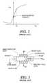
- FIG. 2shows that if low voltages are used for this low power operation, there is a problem with threshold voltages and standby leakage current being of large enough value to degrade overall circuit performance.
- the threshold voltage magnitudesare desirably small, in this example near 0 volts.
- the transistorsuch as an access transistor, will always have a large sub-threshold leakage current.
- CMOS transistorsthat can have relatively large variations in threshold voltage, yet still have relatively low sub-threshold leakage currents at standby.
- dual-gated or double-gated transistor structuresFor example, one technique used in scaling down transistors is referred to as dual-gated or double-gated transistor structures.
- the terminology generally employed in the industryis “dual-gate” if the transistor has a front gate and a back gate which can be driven with separate and independent voltages and “double-gated” to describe structures where both gates are driven with the same potential.
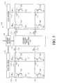
- a dual-gated and/or double-gated MOSFEToffers better device characteristics than conventional bulk silicon MOSFETs. Because a gate electrode is present on both sides of the channel, rather than only on one side as in conventional planar MOSFETs, the electrical field generated by the drain electrode is better screened from the source end of the channel than in conventional planar MOSFETs, as illustrated schematically by the field lines in FIG. 3 .
- the dual-gate and/or double-gate MOSFETturns off and the sub-threshold current is reduced more quickly as the gate voltage is reduced.
- dual gate and/or double gate structuresoffer advantages over conventional bulk silicon MOSFETs, there remains a desire for continued improvement in device performance with continued aggressive scaling. More particularly, there is a need to provide very thin transistor bodies that can control short channel effects with reduced need for extremely high doping levels to avoid the aforementioned difficulties. There is also a need for devices that can be more easily and reliably fabricated.
- the inventionwhich in one embodiment comprises a transistor comprising a vertical annular semiconductive transistor body, a surround gate structure formed around the annular transistor body, a source region formed adjacent a lower portion of the body, and a drain region formed adjacent an upper portion of the body such that the transistor defines a field effect transistor.
- An access array for memory cellscomprising a semiconductive substrate, a plurality of first conductors formed in a first direction along a surface of the substrate, a plurality of transistors formed on the surface of the substrate so as to be offset from associated first conductors and at least partially connected to the associated first conductors, and a plurality of second conductors formed in a second direction and electrically connected with associated transistors such that the transistors can be turned on and off by application of appropriate potentials to the second conductors.
- Yet another embodimentcomprises a method of forming transistor structures comprising forming a pillar vertically extending from a surface of a substrate, growing a single crystalline semiconductive transistor body to extend vertically around the pillar, forming a surround gate structure around the transistor body, forming a source region adjacent lower portions of the transistor body, and forming a drain region adjacent an upper portion of the transistor body.
- various embodimentsprovide an annular, vertical transistor body having ultra-thin dimensions.
- the transistor bodycan be grown which avoids difficulties in sub-lithographic etching based process.
- the transistorscan also be offset from alignment with buried data/bit lines which provides a continuous conductive path extending alongside source regions of the transistors.
- the continuous conductive pathprovides improved conductive characteristics for the data/bit lines, particularly over extended distances.
- FIG. 1is schematic illustration of general relationships of various device parameters/characteristics for a scaling factor k;
- FIG. 2is a graph illustrating sub-threshold leakage in a conventional silicon MOSFET
- FIG. 3is a schematic illustration of a known dual-gate MOSFET
- FIG. 4is a graph illustrating sub-threshold conduction characteristics of conventional bulk silicon MOSFETs and of dual-gate and/or double gate MOSFETs;
- FIG. 5is a circuit schematic illustration of one embodiment of a memory array
- FIG. 6is a top view of one embodiment of a memory access array with access transistors having grown ultra-thin bodies
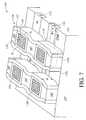
- FIG. 7is a perspective view of one embodiment of a memory access array with access transistors having grown ultra-thin bodies
- FIGS. 8A , 8 B, and 8 Care top, front section, and rear section views respectively of one embodiment of an access transistor with a grown ultra-thin body
- FIGS. 9A , 9 B, and 9 Care side, front, and rear views respectively of surface conduction channels arising in certain embodiments under appropriate applied potentials;
- FIG. 10Aillustrates another embodiment of an ultra-thin body transistor wherein the body is configured generally as a solid pillar
- FIG. 10Billustrates another embodiment of a grown ultra-thin body transistor wherein the body is configured generally as an annular structure encompassing a vertical pillar;
- FIGS. 11 through 14illustrate embodiments of methods of fabrication of a memory array.
- FIG. 5is a schematic circuit diagram of one embodiment of a memory array 100 .
- the memory array 100is configured for storage and retrieval of digital data in a plurality of memory cells 102 comprising the array 100 .
- each memory cell 102comprises an access transistor 104 connected to a charge storage device 106 .
- the charge storage device 106comprises a stacked storage capacitor which will be described in greater detail below.
- the charged storage devices 106store the digital data wherein presence of a predetermined quantity of charge on a charge storage device 106 corresponds to a first data state and wherein absence of the predetermined charge corresponds to a second data state.
- the access transistors 104are connected to corresponding charge storage devices 106 . This provides a selectable electrically conductive path to the charge storage device 106 to provide a path to the charge storage devices 106 for write operations, as well as to evaluate the quantity of charge stored on the charge storage devices 106 in read operations.
- the array 100also comprises one or more row decoder modules 110 which are connected to a plurality of word lines 112 .
- Each word line 112is connected to a corresponding plurality of access transistors 104 .
- the word lines 112 with corresponding access transistors 104are arranged in parallel in what is generally referred to as columns.
- the word lines 112conduct electrical signals which turn on or turn off the corresponding column of access transistors 104 for read and write operations to the corresponding memory cells 102 .
- the array 100also comprises one or more column decoder modules 114 which comprise a plurality of sense amplifiers.
- the one or more column decoders 114are connected to a plurality of data/bit lines 116 .
- the data/bit lines 116are also connected to a plurality of access transistors 104 .
- the data/bit lines 116 with the associated access transistors 104are arranged in parallel in what is generally referred to as a row configuration.
- the word lines 112 and data/bit lines 116are arranged in intersecting directions and, in one particular embodiment, are arranged so as to define a generally rectangular array of the memory cells 102 .
- the data/bit lines 116also conduct signals to the one or more column decoder modules 114 wherein the signals are indicative of the quantity of charge stored on the associated charge storage devices 106 .
- the data/bit lines 116can be utilized to provide the predetermined charge quantity to a charge storage device 106 or to drain the charge from the charge storage device 106 to affect write operations.
- activation of a selected word line 112 and a data bit line 116provides access to the memory cell 102 at the intersection of these selected word line 112 and data/bit line 116 .
- the one or more row decoder modules 110 and one or more column decoder modules 114are also connected to an address buffer 120 .
- the address buffer 120can provide electrical signals corresponding to particular data states to the individual memory cells 102 of the array 100 via the row decoder modules 110 and column decoder modules 114 for write operations. Similarly, the address buffer 120 can receive signals corresponding to the stored data state of the individual memory cells 102 again via the row decoders 110 and column decoders 114 in read operations.
- the address buffer 120is configured for interface with one or more other systems in manners well understood by those of ordinary skill.
- FIG. 6illustrates schematically in a top view one embodiment of access transistors 104 of an array 100 .
- the access transistors 104comprise a vertically extending central pillar 130 (see also FIGS. 7 , 8 b , and 8 c ).
- the central pillar 130extends upward from an upper surface of a semi-conductive substrate 150 .
- the central pillar 130has a generally rectangular or square cross-section.
- the pillar 130describes a generally circular or oval cross-section, a triangular cross-section, or other shape appropriate to the requirements of particular applications.
- the access transistors 104also comprise an annular transistor body 132 which substantially surrounds or encompasses the central pillar 130 along the vertical sides and top of the pillar 130 .
- the annular transistor body 132comprises silicon which is doped to approximately 5 ⁇ 10 17 /cm 2 with boron.
- the annular transistor body 132provides an active transistor region for a field affect transistor structure which will be described in greater detail below.
- the central pillar 130has a lateral or horizontal dimension D 1 of approximately 80 nm or 0.08 ⁇ m.
- the annular transistor body 132has an outer lateral or horizontal dimension D 2 of approximately 120 nm or having an ultra-thin wall thickness T of approximately 20 nm.
- the annular transistor body 132describes a generally vertical hollow annular structure having a wall thickness of approximately 20 nm.
- the annular transistor body 132also has a height H of approximately 100 nm.
- the access transistors 104also comprise a gate dielectric 134 surrounding the annular transistor body 132 .
- the gate dielectric 134describes a generally annular vertically extending structure in contact with the body 132 .
- the gate dielectric 134has similar cross-section to the annular transistor body 132 .
- the access transistors 104also comprise a gate conductor 136 which surrounds or encompasses the gate dielectric 134 .
- the gate conductor 136comprises conductive doped polycrystalline silicon (polysilicon).
- the gate conductor 136is connected at opposed vertical or faces S 1 and S 2 to corresponding word lines 112 .
- each word line 112comprises a separate first word line 112 a and a second word line 112 b .
- the word lines 112 a and 112 bare driven at the same voltage to apply or remove potential from the corresponding gate conductors 136 in concert. In other embodiments, the word lines 112 a and 112 b can be independently driven.
- a dielectric layer or region 140is positioned between adjacent individual access transistors 104 to electrically isolate each access transistor 104 from adjacent neighboring access transistors 104 .
- the gate dielectric structures 134 and dielectric layers 140comprise a single materially continuous layer or region and in other embodiments, the gate dielectric structures 134 and dielectric layer or regions 140 comprise separate structures.
- the access transistors 104are offset from overlying centered alignment with the data/bit lines 116 .
- the access transistors 104are offset laterally by a distance of approximately half the width of the access transistor 104 along the directions of the word lines 112 such that approximately half of the access transistor 104 overlies the corresponding data bit line 116 with the remaining half extending beyond the edge or boundary of the corresponding data/bit line 116 . This provides a region of the data/bit line 116 substantially isolated from the transistor action of the access transistors 104 to improve the conduction characteristics of the data/bit lines 116 as will be described in greater detail below.
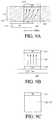
- FIGS. 8A , 8 B, and 8 Cillustrate top, front, and side section views respectively of one embodiment of access transistor 104 in greater detail.
- the annular transistor body 132in this embodiment, encompasses or surrounds the central pillar 130 along vertical sides thereof as well as along an upper surface thereof.
- the annular transistor body 132comprises a single crystalline body region 142 extending upwards from the upper surface of the substrate 150 along the sides or vertical surfaces of the central pillar 130 .
- the single crystalline body region 142comprises a grown region of silicon which is grown along the sides of the vertically extending central pillar 130 .
- the annular transistor body 132also comprises a multiple grain region 144 positioned generally at the top or upper regions of the transistor body 132 .
- the multiple grain region 144comprises a region of the transistor body 132 wherein multiple silicon crystalline structures merge to define a plurality of grain boundaries of a polycrystalline silicon region. Formation of a conduction channel for the transistors 104 occurs substantially in the single crystalline body region 142 rather than in the multiple grain region 144 .
- the grain boundarieshave reduced negative effects on the operational performance of the access transistor 104 as the multiple grain region 144 is utilized to form the drain region 152 which contacts an overlying charge storage device 106 via a drain contact 154 .
- the transistor body 132 as partially overlying the data/bit lines 116also define source regions 146 positioned generally at the lower regions of the transistor body 132 .
- the drain regions 152are positioned at upper regions of the transistor body 132 and in certain embodiments at least partially comprise the multiple grain region 144 .
- the source region 146extends along the lower extent of the transistor body 132 along one side 156 of the transistor body 132 and across approximately half of the adjacent sides.
- the source region 146generally is defined by the portions of the lower regions of the transistor body 132 which overly the associated data/bit line 116 .
- the source regionis present on a first side of the transistor body 132 and substantially absent on the opposite side and extends approximately halfway in-between.
- a continuous conductive path 170( FIG. 8C ) is also defined in the data/bit lines 116 extending adjacent the source regions 146 .
- the continuous conductive path 170provides conductive regions of the data/bit lines 116 that are not significantly involved in the transistor operation of the transistors 104 . This improves the conduction characteristics of the data/bit lines 116 and facilitates further aggressive scaling of the array 100 .
- the source region 146defines a relatively narrow region in lateral extent as compared to a relatively wide drain region 152 .
- the source region 146is generally defined by the overlap of the access transistor 104 and more particularly the transistor body 132 over the underlying data/bit line 116 .
- conduction channels 160will form along the surface of the transistor body 132 and more particularly along the single crystalline body region 142 .
- FIGS. 10A and 10Billustrate schematically two embodiments of access transistor 104 and illustrate generally electron potential distributions in the access transistor 104 .
- FIG. 10Aillustrates in side section view one embodiment of the access transistor 104 wherein the central pillar 130 comprises oxide and the transistor body 132 is configured as an annular vertically extending structure encompassing the central pillar 130 .
- the annular transistor body 132comprises doped silicon.
- the pillar 130 comprising silicon oxidehas a lower dielectric constant than the silicon forming the transistor body 132 .
- FIG. 10Billustrates another embodiment of an access transistor 104 ′ wherein the central pillar 130 and transistor body 132 are merged into a single ultra thin pillar which also provides the transistor body 132 of the access transistor 104 ′.
- potential variations through the silicon pillar 130 , 132 of the access transistor 104 ′will be greater than in the separate transistor body 132 and central oxide pillar 130 .
- transistor action of the access transistor 104 and 104 ′will be similar and the conduction channels 160 will form at the surface of the transistor body 132 or combined pillar 130 ′ and transistor body 132 ′ underneath the adjacent gate dielectric structures 134 .
- the operational characteristics of the access transistor 104will describe a generally steeper sub-threshold slope than for the access transistor 104 ′.
- the combined pillar 130 ′ and transistor body 132 ′ of the access transistor 104 ′will also typically exhibit more body charge than in the access transistor 104 wherein the central pillar 130 comprises oxide and the transistor body 132 is separate and comprises silicon.
- a lower gate voltagewill be required for operation of the access transistor 104 as compared to the access transistor 104 ′.
- the difference in appropriate gate voltage to operate the access transistors 104 , 104 ′will vary depending on the specifics of particular applications. In one embodiment, approximately 30 percent lower gate voltages would be indicated for the embodiment of access transistor 104 , such as illustrated in FIG.
- FIG. 10Ahaving a central pillar 130 comprising oxide with an annular transistor body 132 as compared to the appropriate gate voltages for the embodiment of access transistor 104 ′, such as illustrated in FIG. 10B .
- the lower gate voltage typically required to operate the embodiment of access transistor 104is obtained at the expense of increased steps in the fabrication of this embodiment, as will be described in greater detail below.
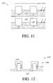
- FIGS. 11 through 14illustrate embodiments of a method 200 of forming a memory array 100 including the access transistors 104 previously described.
- an implant procedure 202is performed to form the plurality of data/bit lines 116 .
- the implant 202is performed with implant parameters of approximately 1 ⁇ 10 15 /cm 2 of boron at approximately 20 keV.
- the pillars 130are then formed to extend upwards from an upper surface of the substrate 150 and to at least partially overlie the underlying implanted data/bit lines 116 .
- the pillars 130are formed such that approximately one-half of the pillar 130 overlies the associated varied data/bit line 116 . Additional details of embodiments of forming the pillars 130 may be found in the co-pending application Ser. No. 11/129,502 filed May 13, 2005 which is incorporated herein by reference in its entirety.
- FIG. 12illustrates subsequent steps in one embodiment of the method 200 wherein a layer of amorphous silicon is deposited as indicated by the reference number 204 so as to overly the upper surface of the substrate 150 as well as the plurality of vertically extending pillars 130 .
- the thickness of amorphous silicon doped with boron 204 depositedwill vary depending on the indications of particular applications, however, in one embodiment, comprises a deposition of approximately 20 nm.
- the amorphous silicon 204is then recrystallized as indicated by the reference number 206 to form the single crystalline body region 142 by a solid phase epitaxial growth process 206 .
- the solid phase epitaxial growth process 206proceeds at parameters of approximately 750° C.
- the solid phase epitaxial growth 206can readily grow the single crystalline structure 142 over such relatively short distances.
- a multiple grain region 144is formed wherein the amorphous silicon 204 is transformed to a polycrystalline silicon structure having grain boundaries.
- this multi-grain region 144will have relatively benign impact on the overall performance of the access transistor 104 as the drain contact 154 to an overlying charge storage device 106 is formed in this multiple grain region 144 .
- FIG. 13illustrates schematically in top view further steps of one embodiment of a method 200 for forming the array 100 comprising the plurality of access transistors 104 .
- FIG. 13illustrates that the previously deposited amorphous silicon 204 has been transformed via a solid phase epitaxial growth process 206 to define the transistor body 132 including the single crystalline body region 142 .
- a gate dielectric formation step 210is performed wherein the gate dielectric 134 is grown or deposited in a well known manner to encompass the transistor body 132 .
- a gate conductor formation step 212is performed to define the gate conductor structure 136 .
- the gate conductor formation 212comprises depositing polysilicon and performing a directional or anisotropic edge, such that the gate dielectric 134 and overlying gate conductor 136 are formed on the sidewalls of the transistor body 132 to define the surround gate structure 138 .
- FIG. 14illustrates one embodiment of further steps in the method 200 of forming a memory array 100 .
- an isolation step 214is performed wherein dielectric material, such as silicon oxide, is filled in the interstitial spaces between adjacent access transistors 104 .
- a planarization step 216is performed in one embodiment by a chemical mechanical planarization/polishing (CMP) process.
- An implantation 218 of arsenic of approximately 1 ⁇ 10 15 /cm 2is performed into the top of the pillars 130 to form the doped drain regions 152 .
- a trench formation step 220is then performed to define a plurality of elongate trenches extending generally in the column direction between adjacent columns of the access transistors 104 .
- a word line formation step 222is performed wherein polysilicon and/or metal is deposited and directionally etched to form the address or word lines 112 positioned along the side walls of the trenches and in contact with the surround gate structures 138 .
- the remainder of the structures for formation of the memory array 100for example, including formation of the overlying charge storage devices 106 , passivation, and formation of interconnect wiring then proceeds according to well known conventional techniques.
- various embodimentsprovide an array of access transistors 104 which have a generally annular vertically extending transistor body having relatively thin side walls, in certain embodiments of a thickness of approximately 20 nm. This provides access transistors 104 which can accommodate continued aggressive scaling with reduced need for relatively high doping levels to suppress short channel effects. Certain embodiments also avoid the requirement for fabricating the access transistors 104 at sub-lithographic dimensions as the transistor body 132 is grown rather than etched.
- a solid phase epitaxial growth processcan provide a single crystalline body region 142 of ultra-thin dimensions in a manner that is easier to fabricate than alternative processes and structures.
Landscapes
- Engineering & Computer Science (AREA)
- Manufacturing & Machinery (AREA)
- Semiconductor Memories (AREA)
Abstract
Description
Claims (11)
Priority Applications (4)
| Application Number | Priority Date | Filing Date | Title |
|---|---|---|---|
| US11/175,677US7888721B2 (en) | 2005-07-06 | 2005-07-06 | Surround gate access transistors with grown ultra-thin bodies |
| US11/557,224US7601595B2 (en) | 2005-07-06 | 2006-11-07 | Surround gate access transistors with grown ultra-thin bodies |
| US11/622,148US7626219B2 (en) | 2005-07-06 | 2007-01-11 | Surround gate access transistors with grown ultra-thin bodies |
| US13/027,154US8115243B2 (en) | 2005-07-06 | 2011-02-14 | Surround gate access transistors with grown ultra-thin bodies |
Applications Claiming Priority (1)
| Application Number | Priority Date | Filing Date | Title |
|---|---|---|---|
| US11/175,677US7888721B2 (en) | 2005-07-06 | 2005-07-06 | Surround gate access transistors with grown ultra-thin bodies |
Related Child Applications (3)
| Application Number | Title | Priority Date | Filing Date |
|---|---|---|---|
| US11/557,224DivisionUS7601595B2 (en) | 2005-07-06 | 2006-11-07 | Surround gate access transistors with grown ultra-thin bodies |
| US11/622,148DivisionUS7626219B2 (en) | 2005-07-06 | 2007-01-11 | Surround gate access transistors with grown ultra-thin bodies |
| US13/027,154DivisionUS8115243B2 (en) | 2005-07-06 | 2011-02-14 | Surround gate access transistors with grown ultra-thin bodies |
Publications (2)
| Publication Number | Publication Date |
|---|---|
| US20070018206A1 US20070018206A1 (en) | 2007-01-25 |
| US7888721B2true US7888721B2 (en) | 2011-02-15 |
Family
ID=37678261
Family Applications (4)
| Application Number | Title | Priority Date | Filing Date |
|---|---|---|---|
| US11/175,677Active2027-11-23US7888721B2 (en) | 2005-07-06 | 2005-07-06 | Surround gate access transistors with grown ultra-thin bodies |
| US11/557,224Active2026-03-01US7601595B2 (en) | 2005-07-06 | 2006-11-07 | Surround gate access transistors with grown ultra-thin bodies |
| US11/622,148Active2026-03-11US7626219B2 (en) | 2005-07-06 | 2007-01-11 | Surround gate access transistors with grown ultra-thin bodies |
| US13/027,154Expired - LifetimeUS8115243B2 (en) | 2005-07-06 | 2011-02-14 | Surround gate access transistors with grown ultra-thin bodies |
Family Applications After (3)
| Application Number | Title | Priority Date | Filing Date |
|---|---|---|---|
| US11/557,224Active2026-03-01US7601595B2 (en) | 2005-07-06 | 2006-11-07 | Surround gate access transistors with grown ultra-thin bodies |
| US11/622,148Active2026-03-11US7626219B2 (en) | 2005-07-06 | 2007-01-11 | Surround gate access transistors with grown ultra-thin bodies |
| US13/027,154Expired - LifetimeUS8115243B2 (en) | 2005-07-06 | 2011-02-14 | Surround gate access transistors with grown ultra-thin bodies |
Country Status (1)
| Country | Link |
|---|---|
| US (4) | US7888721B2 (en) |
Cited By (4)
| Publication number | Priority date | Publication date | Assignee | Title |
|---|---|---|---|---|
| US20110140184A1 (en)* | 2005-07-06 | 2011-06-16 | Leonard Forbes | Surround gate access transistors with grown ultra-thin bodies |
| US20110165744A1 (en)* | 2005-05-13 | 2011-07-07 | Micron Technology | Memory array with ultra-thin etched pillar surround gate access transistors and buried data/bit lines |
| US20120268985A1 (en)* | 2011-04-22 | 2012-10-25 | International Business Machines Corporation | Resonance nanoelectromechanical systems |
| US8350320B2 (en) | 2005-05-13 | 2013-01-08 | Micron Technology, Inc. | Memory array and memory device |
Families Citing this family (38)
| Publication number | Priority date | Publication date | Assignee | Title |
|---|---|---|---|---|
| KR100541515B1 (en)* | 2004-07-22 | 2006-01-11 | 삼성전자주식회사 | Semiconductor device having vertical channel pattern and method of manufacturing same |
| US7326611B2 (en)* | 2005-02-03 | 2008-02-05 | Micron Technology, Inc. | DRAM arrays, vertical transistor structures and methods of forming transistor structures and DRAM arrays |
| US7768051B2 (en) | 2005-07-25 | 2010-08-03 | Micron Technology, Inc. | DRAM including a vertical surround gate transistor |
| EP1793366A3 (en) | 2005-12-02 | 2009-11-04 | Semiconductor Energy Laboratory Co., Ltd. | Semiconductor device, display device, and electronic device |
| US7859026B2 (en)* | 2006-03-16 | 2010-12-28 | Spansion Llc | Vertical semiconductor device |
| US8354311B2 (en)* | 2006-04-04 | 2013-01-15 | Micron Technology, Inc. | Method for forming nanofin transistors |
| US8734583B2 (en)* | 2006-04-04 | 2014-05-27 | Micron Technology, Inc. | Grown nanofin transistors |
| US7425491B2 (en) | 2006-04-04 | 2008-09-16 | Micron Technology, Inc. | Nanowire transistor with surrounding gate |
| US7491995B2 (en) | 2006-04-04 | 2009-02-17 | Micron Technology, Inc. | DRAM with nanofin transistors |
| KR100958798B1 (en)* | 2008-04-04 | 2010-05-24 | 주식회사 하이닉스반도체 | Semiconductor device manufacturing method |
| KR101108178B1 (en) | 2010-07-27 | 2012-01-31 | 삼성모바일디스플레이주식회사 | Thin Film Transistor Sensor and Thin Film Transistor Manufacturing Method |
| JP5228021B2 (en)* | 2010-09-29 | 2013-07-03 | 株式会社東芝 | Semiconductor memory device |
| US8975680B2 (en) | 2011-02-17 | 2015-03-10 | Semiconductor Energy Laboratory Co., Ltd. | Semiconductor memory device and method manufacturing semiconductor memory device |
| US8877593B2 (en) | 2011-07-31 | 2014-11-04 | International Business Machines Corporation | Semiconductor device including an asymmetric feature, and method of making the same |
| US8878156B2 (en) | 2011-11-21 | 2014-11-04 | Avalanche Technology Inc. | Memory device having stitched arrays of 4 F2 memory cells |
| CN102569405B (en)* | 2012-01-17 | 2014-02-19 | 清华大学 | Tunneling transistor with quasi-coaxial cable structure and method of forming same |
| JP6100559B2 (en) | 2012-03-05 | 2017-03-22 | 株式会社半導体エネルギー研究所 | Semiconductor memory device |
| KR20130103942A (en)* | 2012-03-12 | 2013-09-25 | 에스케이하이닉스 주식회사 | Semiconductor device having junctionless vertical gate transistor and method for manufacturing the same |
| US8975705B2 (en) | 2012-05-21 | 2015-03-10 | Unisantis Electronics Singapore Pte. Ltd. | Semiconductor device |
| KR101927991B1 (en) | 2012-07-16 | 2018-12-12 | 에스케이하이닉스 주식회사 | Vertical semiconductor device, module and system having the device and method of the device |
| CN102769016B (en)* | 2012-08-14 | 2015-01-14 | 北京大学 | Anti-radiation complementary metal oxide semiconductor (CMOS) device and preparation method thereof |
| US9064745B2 (en) | 2012-08-29 | 2015-06-23 | International Business Machines Corporation | Sublithographic width finFET employing solid phase epitaxy |
| KR101959388B1 (en)* | 2012-10-04 | 2019-03-19 | 삼성전자주식회사 | Semiconductor device and method of fabricating the same |
| US9093530B2 (en)* | 2012-12-28 | 2015-07-28 | Taiwan Semiconductor Manufacturing Company, Ltd. | Fin structure of FinFET |
| US20150340605A1 (en)* | 2014-05-21 | 2015-11-26 | Kabushiki Kaisha Toshiba | Integrated circuit device |
| WO2017052650A1 (en)* | 2015-09-25 | 2017-03-30 | Intel Corporation | Long channel mos transistors for low leakage applications on a short channel cmos chip |
| US9755073B1 (en)* | 2016-05-11 | 2017-09-05 | International Business Machines Corporation | Fabrication of vertical field effect transistor structure with strained channels |
| KR102519665B1 (en) | 2016-08-05 | 2023-04-07 | 삼성전자주식회사 | Integrated circuit devices and method of manufacturing the same |
| KR102568718B1 (en) | 2016-11-09 | 2023-08-21 | 삼성전자주식회사 | Semiconductor devices |
| US12317511B2 (en)* | 2017-09-06 | 2025-05-27 | Institute of Microelectronics, Chinese Academy of Sciences | MRAM, method of manufacturing the same, and electronic device including the MRAM |
| US10522686B2 (en)* | 2017-09-26 | 2019-12-31 | International Business Machines Corporation | Vertical thin film transistor |
| CN109962068B (en)* | 2017-12-14 | 2020-09-08 | 联华电子股份有限公司 | memory cell |
| US10461185B2 (en) | 2017-12-22 | 2019-10-29 | Micron Technology, Inc. | Assemblies having conductive structures along pillars of semiconductor material |
| US10461173B1 (en) | 2018-05-25 | 2019-10-29 | Globalfoundries Inc. | Methods, apparatus, and manufacturing system for forming source and drain regions in a vertical field effect transistor |
| KR101950146B1 (en)* | 2018-08-23 | 2019-02-19 | 에스케이하이닉스 주식회사 | Semiconductor device having junctionless vertical gate transistor and method for manufacturing the same |
| US20220037519A1 (en)* | 2020-07-29 | 2022-02-03 | Fu-Chang Hsu | Transistor structures and associated processes |
| US11527553B2 (en)* | 2020-07-30 | 2022-12-13 | Taiwan Semiconductor Manufacturing Co., Ltd. | Three-dimensional memory device and method |
| CN113690317A (en)* | 2021-08-19 | 2021-11-23 | 福建晋润半导体技术有限公司 | Planar power MOSFET device with super junction structure and manufacturing method thereof |
Citations (374)
| Publication number | Priority date | Publication date | Assignee | Title |
|---|---|---|---|---|
| US3731287A (en) | 1971-07-02 | 1973-05-01 | Gen Instrument Corp | Single device memory system having shift register output characteristics |
| US3732287A (en) | 1969-09-09 | 1973-05-08 | Basf Ag | Bismonocarboxylic esters of 3-formylbutanediol-1,2 |
| US3941629A (en) | 1974-04-11 | 1976-03-02 | General Motors Corporation | Diaphragm formation on silicon substrate |
| US4139442A (en) | 1977-09-13 | 1979-02-13 | International Business Machines Corporation | Reactive ion etching method for producing deep dielectric isolation in silicon |
| US4234362A (en) | 1978-11-03 | 1980-11-18 | International Business Machines Corporation | Method for forming an insulator between layers of conductive material |
| US4333964A (en) | 1980-09-15 | 1982-06-08 | General Electric Company | Method of making integrated circuits |
| US4419809A (en) | 1981-12-30 | 1983-12-13 | International Business Machines Corporation | Fabrication process of sub-micrometer channel length MOSFETs |
| US4432132A (en) | 1981-12-07 | 1984-02-21 | Bell Telephone Laboratories, Incorporated | Formation of sidewall oxide layers by reactive oxygen ion etching to define submicron features |
| US4470062A (en) | 1979-08-31 | 1984-09-04 | Hitachi, Ltd. | Semiconductor device having isolation regions |
| US4472459A (en) | 1983-10-24 | 1984-09-18 | Rca Corporation | Local oxidation of silicon substrate using LPCVD silicon nitride |
| US4502914A (en) | 1982-11-13 | 1985-03-05 | International Business Machines Corporation | Method of making structures with dimensions in the sub-micrometer range |
| US4508579A (en) | 1981-03-30 | 1985-04-02 | International Business Machines Corporation | Lateral device structures using self-aligned fabrication techniques |
| US4508757A (en) | 1982-12-20 | 1985-04-02 | International Business Machines Corporation | Method of manufacturing a minimum bird's beak recessed oxide isolation structure |
| US4551910A (en) | 1984-11-27 | 1985-11-12 | Intel Corporation | MOS Isolation processing |
| US4570325A (en) | 1983-12-16 | 1986-02-18 | Kabushiki Kaisha Toshiba | Manufacturing a field oxide region for a semiconductor device |
| US4615762A (en) | 1985-04-30 | 1986-10-07 | Rca Corporation | Method for thinning silicon |
| US4630356A (en) | 1985-09-19 | 1986-12-23 | International Business Machines Corporation | Method of forming recessed oxide isolation with reduced steepness of the birds' neck |
| US4648937A (en) | 1985-10-30 | 1987-03-10 | International Business Machines Corporation | Method of preventing asymmetric etching of lines in sub-micrometer range sidewall images transfer |
| EP0227303A2 (en) | 1985-11-25 | 1987-07-01 | Plessey Overseas Limited | Method of manufacturing semiconductor devices having side-wall isolation |
| US4716131A (en) | 1983-11-28 | 1987-12-29 | Nec Corporation | Method of manufacturing semiconductor device having polycrystalline silicon layer with metal silicide film |
| US4746630A (en) | 1986-09-17 | 1988-05-24 | Hewlett-Packard Company | Method for producing recessed field oxide with improved sidewall characteristics |
| US4776922A (en) | 1987-10-30 | 1988-10-11 | International Business Machines Corporation | Formation of variable-width sidewall structures |
| US4789560A (en) | 1986-01-08 | 1988-12-06 | Advanced Micro Devices, Inc. | Diffusion stop method for forming silicon oxide during the fabrication of IC devices |
| US4838991A (en) | 1987-10-30 | 1989-06-13 | International Business Machines Corporation | Process for defining organic sidewall structures |
| US4903344A (en) | 1987-07-07 | 1990-02-20 | Oki Electric Industry Co., Ltd. | Semiconductor memory device with staggered sense amplifiers |
| DD280851A1 (en) | 1989-03-27 | 1990-07-18 | Dresden Forschzentr Mikroelek | METHOD OF MAKING TRENCH MEMORY CELLS |
| US4959325A (en) | 1989-02-24 | 1990-09-25 | Micron Technology, Inc. | Reduction of electric field effect in the bird's beak region of a DRAM cell following expansion of active region through local encroachment reduction |
| US4965221A (en) | 1989-03-15 | 1990-10-23 | Micron Technology, Inc. | Spacer isolation method for minimizing parasitic sidewall capacitance and creating fully recessed field oxide regions |
| US4983544A (en) | 1986-10-20 | 1991-01-08 | International Business Machines Corporation | Silicide bridge contact process |
| US5013680A (en) | 1990-07-18 | 1991-05-07 | Micron Technology, Inc. | Process for fabricating a DRAM array having feature widths that transcend the resolution limit of available photolithography |
| US5041898A (en) | 1987-09-08 | 1991-08-20 | Mitsubishi Denki Kabushiki Kaisha | Interconnection layer formed on embedded dielectric and method for manufacturing the same |
| US5047117A (en) | 1990-09-26 | 1991-09-10 | Micron Technology, Inc. | Method of forming a narrow self-aligned, annular opening in a masking layer |
| US5053105A (en) | 1990-07-19 | 1991-10-01 | Micron Technology, Inc. | Process for creating an etch mask suitable for deep plasma etches employing self-aligned silicidation of a metal layer masked with a silicon dioxide template |
| US5057449A (en) | 1990-03-26 | 1991-10-15 | Micron Technology, Inc. | Process for creating two thicknesses of gate oxide within a dynamic random access memory |
| US5087586A (en) | 1991-07-03 | 1992-02-11 | Micron Technology, Inc. | Process for creating fully-recessed field isolation regions by oxidizing a selectively-grown epitaxial silicon layer |
| US5117027A (en) | 1990-10-31 | 1992-05-26 | Huls Aktiengesellschaft | Process for the preparation of organosilanes containing methacryloyloxy or acryloyloxy groups |
| US5122848A (en) | 1991-04-08 | 1992-06-16 | Micron Technology, Inc. | Insulated-gate vertical field-effect transistor with high current drive and minimum overlap capacitance |
| US5128274A (en) | 1989-08-01 | 1992-07-07 | Matsushita Electric Industrial Co., Ltd. | Method for producing a semiconductor device having a LOCOS insulating film with at least two different thickness |
| US5149669A (en) | 1987-03-06 | 1992-09-22 | Seiko Instruments Inc. | Method of forming an isolation region in a semiconductor device |
| EP0491408A3 (en) | 1990-11-20 | 1992-10-28 | Consorzio Per La Ricerca Sulla Microelettronica Nel Mezzogiorno | Process for making planarized sub-micrometric trenches in integrated circuits |
| US5210046A (en) | 1989-12-22 | 1993-05-11 | Scs-Thomas Microelectronics S.R.L. | Method of fabricating eprom device with metallic source connections |
| US5252504A (en) | 1988-05-02 | 1993-10-12 | Micron Technology, Inc. | Reverse polysilicon CMOS fabrication |
| US5260229A (en) | 1991-08-30 | 1993-11-09 | Sgs-Thomson Microelectronics, Inc. | Method of forming isolated regions of oxide |
| US5295092A (en) | 1992-01-21 | 1994-03-15 | Sharp Kabushiki Kaisha | Semiconductor read only memory |
| US5305252A (en) | 1990-07-06 | 1994-04-19 | Nec Corporation | Semiconductor memory device having memory cell matrix obliquely arranged with respect to bit lines |
| DE4236609A1 (en) | 1992-10-29 | 1994-05-05 | Siemens Ag | Method for forming a structure in the surface of a substrate - with an auxiliary structure laterally bounding an initial masking structure, followed by selective removal of masking structure using the auxiliary structure as an etching mask |
| US5316966A (en) | 1990-09-28 | 1994-05-31 | U.S. Philips Corporation | Method of providing mask alignment marks |
| US5319753A (en) | 1992-09-29 | 1994-06-07 | Zilog, Inc. | Queued interrupt mechanism with supplementary command/status/message information |
| US5328810A (en) | 1990-05-07 | 1994-07-12 | Micron Technology, Inc. | Method for reducing, by a factor or 2-N, the minimum masking pitch of a photolithographic process |
| US5330879A (en) | 1992-07-16 | 1994-07-19 | Micron Technology, Inc. | Method for fabrication of close-tolerance lines and sharp emission tips on a semiconductor wafer |
| US5334548A (en) | 1988-06-01 | 1994-08-02 | Texas Instruments Incorporated | High performance composed pillar dRAM cell |
| DE4408764A1 (en) | 1993-03-15 | 1994-09-22 | Toshiba Kawasaki Kk | Semiconductor arrangement |
| US5358894A (en) | 1992-02-06 | 1994-10-25 | Micron Technology, Inc. | Oxidation enhancement in narrow masked field regions of a semiconductor wafer |
| US5374572A (en) | 1993-07-22 | 1994-12-20 | Motorola, Inc. | Method of forming a transistor having an offset channel section |
| US5409563A (en) | 1993-02-26 | 1995-04-25 | Micron Technology, Inc. | Method for etching high aspect ratio features |
| US5414287A (en) | 1994-04-25 | 1995-05-09 | United Microelectronics Corporation | Process for high density split-gate memory cell for flash or EPROM |
| US5416350A (en) | 1993-03-15 | 1995-05-16 | Kabushiki Kaisha Toshiba | Semiconductor device with vertical transistors connected in series between bit lines |
| US5438016A (en) | 1994-03-02 | 1995-08-01 | Micron Semiconductor, Inc. | Method of semiconductor device isolation employing polysilicon layer for field oxide formation |
| US5457067A (en) | 1993-10-14 | 1995-10-10 | Goldstar Electron Co., Ltd. | Process for formation of an isolating layer for a semiconductor device |
| US5458999A (en) | 1993-06-24 | 1995-10-17 | Szabo; Gabor | Interferometric phase shifting method for high resolution microlithography |
| US5466632A (en) | 1994-05-26 | 1995-11-14 | United Microelectronics Corp. | Field oxide with curvilinear boundaries and method of producing the same |
| US5468675A (en) | 1993-05-26 | 1995-11-21 | Rohm Co., Ltd. | Method for manufacturing a device separation region for semiconductor device |
| US5497017A (en) | 1995-01-26 | 1996-03-05 | Micron Technology, Inc. | Dynamic random access memory array having a cross-point layout, tungsten digit lines buried in the substrate, and vertical access transistors |
| US5514885A (en) | 1986-10-09 | 1996-05-07 | Myrick; James J. | SOI methods and apparatus |
| US5539229A (en) | 1994-12-28 | 1996-07-23 | International Business Machines Corporation | MOSFET with raised STI isolation self-aligned to the gate stack |
| US5561308A (en)* | 1994-01-18 | 1996-10-01 | Kabushiki Kaisha Toshiba | Semiconductor device including thin film transistor |
| US5563012A (en) | 1994-06-30 | 1996-10-08 | International Business Machines Corporation | Multi mask method for selective mask feature enhancement |
| US5569620A (en) | 1992-09-03 | 1996-10-29 | Harris Corporation | Bonded wafer processing with metal silicidation |
| US5583065A (en) | 1994-11-23 | 1996-12-10 | Sony Corporation | Method of making a MOS semiconductor device |
| US5596759A (en) | 1989-11-03 | 1997-01-21 | Compaq Computer Corporation | Method for initializing a multiple processor computer system using a common ROM |
| US5604159A (en) | 1994-01-31 | 1997-02-18 | Motorola, Inc. | Method of making a contact structure |
| US5607874A (en) | 1996-02-02 | 1997-03-04 | Taiwan Semiconductor Manufacturing Company, Ltd. | Method for fabricating a DRAM cell with a T shaped storage capacitor |
| US5638318A (en) | 1995-09-11 | 1997-06-10 | Micron Technology, Inc. | Ferroelectric memory using ferroelectric reference cells |
| US5670794A (en) | 1994-10-07 | 1997-09-23 | Micron Technology, Inc. | Thin film transistors |
| US5675164A (en) | 1995-06-07 | 1997-10-07 | International Business Machines Corporation | High performance multi-mesa field effect transistor |
| US5677865A (en) | 1995-09-11 | 1997-10-14 | Micron Technology, Inc. | Ferroelectric memory using reference charge circuit |
| US5679591A (en) | 1996-12-16 | 1997-10-21 | Taiwan Semiconductor Manufacturing Company, Ltd | Method of making raised-bitline contactless trenched flash memory cell |
| US5680344A (en) | 1995-09-11 | 1997-10-21 | Micron Technology, Inc. | Circuit and method of operating a ferrolectric memory in a DRAM mode |
| US5700733A (en) | 1995-06-27 | 1997-12-23 | Micron Technology, Inc. | Semiconductor processing methods of forming field oxide regions on a semiconductor substrate |
| US5705321A (en) | 1993-09-30 | 1998-01-06 | The University Of New Mexico | Method for manufacture of quantum sized periodic structures in Si materials |
| US5748519A (en) | 1996-12-13 | 1998-05-05 | Motorola, Inc. | Method of selecting a memory cell in a magnetic random access memory device |
| US5747377A (en) | 1996-09-06 | 1998-05-05 | Powerchip Semiconductor Corp. | Process for forming shallow trench isolation |
| US5753546A (en) | 1995-06-30 | 1998-05-19 | Hyundai Electronics Industries Co., Ltd. | Method for fabricating metal oxide field effect transistors |
| US5756395A (en) | 1995-08-18 | 1998-05-26 | Lsi Logic Corporation | Process for forming metal interconnect structures for use with integrated circuit devices to form integrated circuit structures |
| US5780349A (en) | 1997-02-20 | 1998-07-14 | National Semiconductor Corporation | Self-aligned MOSFET gate/source/drain salicide formation |
| US5789306A (en) | 1996-04-18 | 1998-08-04 | Micron Technology, Inc. | Dual-masked field isolation |
| US5789269A (en) | 1995-07-11 | 1998-08-04 | Advanced Micro Devices, Inc. | Field implant for semiconductor device |
| US5789320A (en) | 1996-04-23 | 1998-08-04 | International Business Machines Corporation | Plating of noble metal electrodes for DRAM and FRAM |
| US5795830A (en) | 1995-06-06 | 1998-08-18 | International Business Machines Corporation | Reducing pitch with continuously adjustable line and space dimensions |
| US5798544A (en) | 1994-04-22 | 1998-08-25 | Nec Corporation | Semiconductor memory device having trench isolation regions and bit lines formed thereover |
| US5804458A (en) | 1996-12-16 | 1998-09-08 | Motorola, Inc. | Method of fabricating spaced apart submicron magnetic memory cells |
| US5821600A (en) | 1994-12-20 | 1998-10-13 | Stmicroelectronics, Inc. | Isolation by active transistors with grounded gates |
| US5834359A (en) | 1997-08-29 | 1998-11-10 | Vanguard International Semiconductor Corporation | Method of forming an isolation region in a semiconductor substrate |
| US5841611A (en) | 1994-05-02 | 1998-11-24 | Matsushita Electric Industrial Co., Ltd. | Magnetoresistance effect device and magnetoresistance effect type head, memory device, and amplifying device using the same |
| US5861328A (en) | 1996-10-07 | 1999-01-19 | Motorola, Inc. | Method of fabricating GMR devices |
| US5864496A (en) | 1997-09-29 | 1999-01-26 | Siemens Aktiengesellschaft | High density semiconductor memory having diagonal bit lines and dual word lines |
| US5892708A (en) | 1992-09-24 | 1999-04-06 | Nonvolatile Electronics, Incorporated | Magnetoresistive memory using large fraction of memory cell films for data storage |
| US5895273A (en) | 1997-06-27 | 1999-04-20 | International Business Machines Corporation | Silicon sidewall etching |
| US5895238A (en) | 1996-12-12 | 1999-04-20 | Nec Corporation | Doping technique for MOS devices |
| US5899727A (en) | 1996-05-02 | 1999-05-04 | Advanced Micro Devices, Inc. | Method of making a semiconductor isolation region bounded by a trench and covered with an oxide to improve planarization |
| US5902690A (en) | 1997-02-25 | 1999-05-11 | Motorola, Inc. | Stray magnetic shielding for a non-volatile MRAM |
| US5905285A (en) | 1996-09-12 | 1999-05-18 | Advanced Micro Devices, Inc. | Ultra short trench transistors and process for making same |
| US5907170A (en) | 1997-10-06 | 1999-05-25 | Micron Technology, Inc. | Circuit and method for an open bit line memory cell with a vertical transistor and trench plate trench capacitor |
| US5909618A (en) | 1997-07-08 | 1999-06-01 | Micron Technology, Inc. | Method of making memory cell with vertical transistor and buried word and body lines |
| US5917745A (en) | 1997-09-18 | 1999-06-29 | Fujitsu Limited | Semiconductor memory device |
| US5917749A (en) | 1997-05-23 | 1999-06-29 | Motorola, Inc. | MRAM cell requiring low switching field |
| US5956267A (en) | 1997-12-18 | 1999-09-21 | Honeywell Inc | Self-aligned wordline keeper and method of manufacture therefor |
| US5963803A (en) | 1998-02-02 | 1999-10-05 | Advanced Micro Devices, Inc. | Method of making N-channel and P-channel IGFETs with different gate thicknesses and spacer widths |
| US5963469A (en) | 1998-02-24 | 1999-10-05 | Micron Technology, Inc. | Vertical bipolar read access for low voltage memory cell |
| US5977579A (en) | 1998-12-03 | 1999-11-02 | Micron Technology, Inc. | Trench dram cell with vertical device and buried word lines |
| US5981318A (en) | 1995-02-28 | 1999-11-09 | Stmicroelectronics, Inc. | Fully-dielectric-isolated FET technology |
| US5998256A (en) | 1996-11-01 | 1999-12-07 | Micron Technology, Inc. | Semiconductor processing methods of forming devices on a substrate, forming device arrays on a substrate, forming conductive lines on a substrate, and forming capacitor arrays on a substrate, and integrated circuitry |
| US6005800A (en) | 1998-11-23 | 1999-12-21 | International Business Machines Corporation | Magnetic memory array with paired asymmetric memory cells for improved write margin |
| US6004862A (en) | 1998-01-20 | 1999-12-21 | Advanced Micro Devices, Inc. | Core array and periphery isolation technique |
| US6008106A (en) | 1997-07-15 | 1999-12-28 | Mosel Vitelic Inc. | Micro-trench oxidation by using rough oxide mask for field isolation |
| US6010946A (en) | 1996-08-21 | 2000-01-04 | Nec Corporation | Semiconductor device with isolation insulating film tapered and method of manufacturing the same |
| US6042998A (en) | 1993-09-30 | 2000-03-28 | The University Of New Mexico | Method and apparatus for extending spatial frequencies in photolithography images |
| US6049106A (en)* | 1999-01-14 | 2000-04-11 | Micron Technology, Inc. | Large grain single crystal vertical thin film polysilicon MOSFETs |
| US6057573A (en) | 1998-05-27 | 2000-05-02 | Vanguard International Semiconductor Corporation | Design for high density memory with relaxed metal pitch |
| US6063688A (en) | 1997-09-29 | 2000-05-16 | Intel Corporation | Fabrication of deep submicron structures and quantum wire transistors using hard-mask transistor width definition |
| US6066869A (en) | 1997-10-06 | 2000-05-23 | Micron Technology, Inc. | Circuit and method for a folded bit line memory cell with vertical transistor and trench capacitor |
| US6066191A (en) | 1997-05-21 | 2000-05-23 | Kabushiki Kaisha Toyota Chuo Kenkyusho | Hard molybdenum alloy, wear resistant alloy and method for manufacturing the same |
| US6071789A (en) | 1998-11-10 | 2000-06-06 | Vanguard International Semiconductor Corporation | Method for simultaneously fabricating a DRAM capacitor and metal interconnections |
| US6072209A (en) | 1997-07-08 | 2000-06-06 | Micro Technology, Inc. | Four F2 folded bit line DRAM cell structure having buried bit and word lines |
| US6077745A (en) | 1997-01-22 | 2000-06-20 | International Business Machines Corporation | Self-aligned diffused source vertical transistors with stack capacitors in a 4F-square memory cell array |
| DE19928781C1 (en) | 1999-06-23 | 2000-07-06 | Siemens Ag | DRAM cell array has deep word line trenches for increasing transistor channel length and has no fixed potential word lines separating adjacent memory cells |
| US6097065A (en) | 1998-03-30 | 2000-08-01 | Micron Technology, Inc. | Circuits and methods for dual-gated transistors |
| US6104633A (en) | 1998-02-10 | 2000-08-15 | International Business Machines Corporation | Intentional asymmetry imposed during fabrication and/or access of magnetic tunnel junction devices |
| US6104068A (en) | 1998-09-01 | 2000-08-15 | Micron Technology, Inc. | Structure and method for improved signal processing |
| US6121148A (en) | 1998-02-17 | 2000-09-19 | National Semiconductor Corporation | Semiconductor device trench isolation structure with polysilicon bias voltage contact |
| US6134139A (en) | 1999-07-28 | 2000-10-17 | Hewlett-Packard | Magnetic memory structure with improved half-select margin |
| US6141204A (en) | 1996-01-03 | 2000-10-31 | Micron Technology, Inc. | Capacitor constructions and semiconductor processing method of forming capacitor constructions |
| US6147405A (en) | 1998-02-19 | 2000-11-14 | Micron Technology, Inc. | Asymmetric, double-sided self-aligned silicide and method of forming the same |
| US6150211A (en) | 1996-12-11 | 2000-11-21 | Micron Technology, Inc. | Methods of forming storage capacitors in integrated circuitry memory cells and integrated circuitry |
| US6150687A (en) | 1997-07-08 | 2000-11-21 | Micron Technology, Inc. | Memory cell having a vertical transistor with buried source/drain and dual gates |
| US6150688A (en) | 1994-05-26 | 2000-11-21 | Mitsubishi Denki Kabushiki Kaisha | Semiconductor device and method of manufacturing the same |
| US6157064A (en) | 1997-12-15 | 2000-12-05 | Taiwan Semiconductor Manufacturing Company Ltd. | Method and a deep sub-micron field effect transistor structure for suppressing short channel effects |
| US6165833A (en) | 1997-12-19 | 2000-12-26 | Micron Technology, Inc. | Semiconductor processing method of forming a capacitor |
| US6172391B1 (en) | 1997-08-27 | 2001-01-09 | Siemens Aktiengesellschaft | DRAM cell arrangement and method for the manufacture thereof |
| US6175146B1 (en) | 1997-03-13 | 2001-01-16 | Micron Technology, Inc. | Semiconductor processing methods of forming integrated circuitry memory devices, methods of forming capacitor containers, methods of making electrical connection to circuit nodes and related integrated circuitry |
| US6174780B1 (en) | 1996-04-08 | 2001-01-16 | Micron Technology, Inc. | Method of preparing integrated circuit devices containing isolated dielectric material |
| US6191470B1 (en) | 1997-07-08 | 2001-02-20 | Micron Technology, Inc. | Semiconductor-on-insulator memory cell with buried word and body lines |
| US6211044B1 (en) | 1999-04-12 | 2001-04-03 | Advanced Micro Devices | Process for fabricating a semiconductor device component using a selective silicidation reaction |
| US6229169B1 (en) | 1997-12-17 | 2001-05-08 | Infineon Technologies Ag | Memory cell configuration, method for fabricating it and methods for operating it |
| US6236590B1 (en) | 2000-07-21 | 2001-05-22 | Hewlett-Packard Company | Optimal write conductors layout for improved performance in MRAM |
| US6238976B1 (en) | 1997-07-08 | 2001-05-29 | Micron Technology, Inc. | Method for forming high density flash memory |
| US6246083B1 (en) | 1998-02-24 | 2001-06-12 | Micron Technology, Inc. | Vertical gain cell and array for a dynamic random access memory |
| US20010005631A1 (en) | 1999-12-14 | 2001-06-28 | Jin-Won Kim | Method for manufacturing an electrode of a capacitor |
| US6265742B1 (en) | 1998-03-04 | 2001-07-24 | Siemens Aktiengesellschaft | Memory cell structure and fabrication |
| US6271080B1 (en) | 1999-12-16 | 2001-08-07 | International Business Machines Corporation | Structure and method for planar MOSFET DRAM cell free of wordline gate conductor to storage trench overlay sensitivity |
| US6274905B1 (en) | 1999-06-30 | 2001-08-14 | Fairchild Semiconductor Corporation | Trench structure substantially filled with high-conductivity material |
| US6282113B1 (en) | 1999-09-29 | 2001-08-28 | International Business Machines Corporation | Four F-squared gapless dual layer bitline DRAM array architecture |
| US20010019870A1 (en) | 1997-04-25 | 2001-09-06 | Noble Wendell P. | Semiconductor processing methods of forming integrated circuitry, forming conductive lines, forming a conductive grid, forming a conductive network, forming an electrical interconnection to a node location forming an electrical interconnection with a transistor source/drain region, and integrated circuitry |
| US6288454B1 (en) | 1999-05-13 | 2001-09-11 | Lsi Logic Corporation | Semiconductor wafer having a layer-to-layer alignment mark and method for fabricating the same |
| US6291334B1 (en) | 1997-12-19 | 2001-09-18 | Applied Materials, Inc. | Etch stop layer for dual damascene process |
| EP1061592A3 (en) | 1999-06-17 | 2001-09-26 | Matsushita Electric Industrial Co., Ltd. | Magneto-resistance effect element, and its use as memory element |
| US6297554B1 (en) | 2000-03-10 | 2001-10-02 | United Microelectronics Corp. | Dual damascene interconnect structure with reduced parasitic capacitance |
| US6306727B1 (en) | 1997-08-18 | 2001-10-23 | Micron Technology, Inc. | Advanced isolation process for large memory arrays |
| US6316309B1 (en) | 1998-06-09 | 2001-11-13 | Steven John Holmes | Method of forming self-isolated and self-aligned 4F-square vertical FET-trench DRAM cells |
| US6320222B1 (en) | 1998-09-01 | 2001-11-20 | Micron Technology, Inc. | Structure and method for reducing threshold voltage variations due to dopant fluctuations |
| US20020000608A1 (en) | 2000-06-02 | 2002-01-03 | Hirofumi Harada | Vertical MOS transistor and a method of manufacturing the same |
| US20020005590A1 (en) | 1996-01-26 | 2002-01-17 | Brent Keeth | Digit line architecture for dynamic memory |
| US6348380B1 (en) | 2000-08-25 | 2002-02-19 | Micron Technology, Inc. | Use of dilute steam ambient for improvement of flash devices |
| US20020024081A1 (en) | 2000-08-27 | 2002-02-28 | Achim Gratz | Vertical non-volatile semiconductor memory cell and method for manufaturing the memory cell |
| US20020028541A1 (en) | 2000-08-14 | 2002-03-07 | Lee Thomas H. | Dense arrays and charge storage devices, and methods for making same |
| US20020030214A1 (en) | 2000-09-11 | 2002-03-14 | Fumio Horiguchi | Semiconductor device and method for manufacturing the same |
| US6362057B1 (en) | 1999-10-26 | 2002-03-26 | Motorola, Inc. | Method for forming a semiconductor device |
| US20020038886A1 (en) | 1999-03-31 | 2002-04-04 | Mo Brian Sze-Ki | Method of forming trench transistor with self-aligned source |
| US6368950B1 (en) | 2000-12-12 | 2002-04-09 | Advanced Micro Devices, Inc. | Silicide gate transistors |
| US20020042198A1 (en) | 2000-09-20 | 2002-04-11 | Bjarni Bjarnason | Method in etching of a substrate |
| US20020045308A1 (en) | 1996-11-01 | 2002-04-18 | Werner Juengling | Semiconductor processing methods of forming a plurality of capacitors on a substrate, bit line contacts and method of forming bit line contacts |
| US6377070B1 (en) | 2001-02-09 | 2002-04-23 | Micron Technology, Inc. | In-service programmable logic arrays with ultra thin vertical body transistors |
| US6383907B1 (en) | 1999-09-08 | 2002-05-07 | Sony Corporation | Process for fabricating a semiconductor device |
| US6391782B1 (en) | 2000-06-20 | 2002-05-21 | Advanced Micro Devices, Inc. | Process for forming multiple active lines and gate-all-around MOSFET |
| US20020061639A1 (en) | 2000-10-02 | 2002-05-23 | Kazuichiroh Itonaga | Semiconductor device and method for manufacturing the same |
| US6396096B1 (en) | 2000-06-21 | 2002-05-28 | International Business Machines Corporation | Design layout for a dense memory cell structure |
| US20020063110A1 (en) | 2000-11-30 | 2002-05-30 | Cantell Marc W. | Etching of hard masks |
| US6404056B1 (en) | 1994-01-20 | 2002-06-11 | Mitsubishi Denki Kabushiki Kaisha | Semiconductor integrated circuit |
| US6424001B1 (en) | 2001-02-09 | 2002-07-23 | Micron Technology, Inc. | Flash memory with ultra thin vertical body transistors |
| US6424561B1 (en) | 2000-07-18 | 2002-07-23 | Micron Technology, Inc. | MRAM architecture using offset bits for increased write selectivity |
| US6423474B1 (en) | 2000-03-21 | 2002-07-23 | Micron Technology, Inc. | Use of DARC and BARC in flash memory processing |
| US20020106772A1 (en) | 1998-10-15 | 2002-08-08 | Washington State University Research Foundation | Geranyl diphosphate synthase large subunit, and methods of use |
| US6440801B1 (en) | 1997-01-22 | 2002-08-27 | International Business Machines Corporation | Structure for folded architecture pillar memory cell |
| US20020123216A1 (en) | 2001-03-05 | 2002-09-05 | Natsuki Yokoyama | Method of manufacturing semiconductor device |
| US20020121673A1 (en) | 2000-08-31 | 2002-09-05 | Keiji Jono | Methods of forming an isolation trench in a semiconductor, methods of forming an isolation trench in a surface of a silicon wafer, methods of forming an isolation trench-isolated transistor, trench-isolated transistor, trench isolation structures formed in a semiconductor, memory cells and DRAMs |
| US6448601B1 (en) | 2001-02-09 | 2002-09-10 | Micron Technology, Inc. | Memory address and decode circuits with ultra thin body transistors |
| US20020127810A1 (en) | 2000-05-29 | 2002-09-12 | Fujitsu Limited | Semiconductor device and method for fabricating the same |
| US20020130686A1 (en) | 2001-03-14 | 2002-09-19 | Micron Technology, Inc. | CMOS gate array with vertical transistors |
| US20020130348A1 (en) | 2001-03-16 | 2002-09-19 | Tran Luan C. | 6F2 dram array, a dram array formed on a semiconductive substrate, a method of forming memory cells in a 6F2 dram array and a method of isolating a single row of memory cells in a 6F2 dram array |
| US6455372B1 (en) | 2000-08-14 | 2002-09-24 | Micron Technology, Inc. | Nucleation for improved flash erase characteristics |
| US20020135029A1 (en) | 2001-03-23 | 2002-09-26 | Er-Xuan Ping | Method for forming raised structures by controlled selective epitaxial growth of facet using spacer |
| US6459119B1 (en) | 1998-06-09 | 2002-10-01 | Macronix International Co., Ltd. | Contact array structure for buried type transistor |
| US6458662B1 (en) | 2001-04-04 | 2002-10-01 | Advanced Micro Devices, Inc. | Method of fabricating a semiconductor device having an asymmetrical dual-gate silicon-germanium (SiGe) channel MOSFET and a device thereby formed |
| US6468887B2 (en) | 1997-04-04 | 2002-10-22 | Nippon Steel Corporation | Semiconductor device and a method of manufacturing the same |
| US20020158273A1 (en) | 2000-10-17 | 2002-10-31 | Hitachi, Ltd. | Nonvolatile semiconductor memory device and a method of manufacturing the same |
| US6475869B1 (en) | 2001-02-26 | 2002-11-05 | Advanced Micro Devices, Inc. | Method of forming a double gate transistor having an epitaxial silicon/germanium channel region |
| US6475867B1 (en) | 2001-04-02 | 2002-11-05 | Advanced Micro Devices, Inc. | Method of forming integrated circuit features by oxidation of titanium hard mask |
| US20020187356A1 (en) | 2000-12-14 | 2002-12-12 | Weeks T. Warren | Gallium nitride materials and methods |
| WO2002099864A1 (en) | 2001-05-31 | 2002-12-12 | Infineon Technologies, Ag | Method for removing polysilane from a semiconductor without stripping |
| US6496034B2 (en) | 2001-02-09 | 2002-12-17 | Micron Technology, Inc. | Programmable logic arrays with ultra thin body transistors |
| US6498062B2 (en) | 2001-04-27 | 2002-12-24 | Micron Technology, Inc. | DRAM access transistor |
| US20030001290A1 (en) | 2001-06-29 | 2003-01-02 | Kabushiki Kaisha Toshiba | Semiconductor memory device and method for manufacturing the same |
| US20030006410A1 (en) | 2000-03-01 | 2003-01-09 | Brian Doyle | Quantum wire gate device and method of making same |
| US20030015757A1 (en) | 2001-07-19 | 2003-01-23 | Takashi Ohsawa | Semiconductor memory device |
| US6514884B2 (en) | 1998-02-06 | 2003-02-04 | Semiconductor Process Laboratory Co., Ltd. | Method for reforming base surface, method for manufacturing semiconductor device and equipment for manufacturing the same |
| US6522584B1 (en) | 2001-08-02 | 2003-02-18 | Micron Technology, Inc. | Programming methods for multi-level flash EEPROMs |
| US20030040186A1 (en) | 1999-03-23 | 2003-02-27 | Micron Technology, Inc. | Methods of forming materials over uneven surface topologies, and methods of forming insulative materials over and between conductive lines |
| US20030042542A1 (en) | 1996-04-26 | 2003-03-06 | Shigeto Maegawa | Semiconductor device having a thin film transistor and manufacturing method thereof |
| US20030044722A1 (en) | 2001-08-28 | 2003-03-06 | Yi-Yu Hsu | Process for improving critical dimension uniformity |
| US6531727B2 (en) | 2001-02-09 | 2003-03-11 | Micron Technology, Inc. | Open bit line DRAM with ultra thin body transistors |
| US6534243B1 (en) | 2000-10-23 | 2003-03-18 | Advanced Micro Devices, Inc. | Chemical feature doubling process |
| US6537870B1 (en) | 2000-09-29 | 2003-03-25 | Infineon Technologies Ag | Method of forming an integrated circuit comprising a self aligned trench |
| US6538916B2 (en) | 2001-02-15 | 2003-03-25 | Kabushiki Kaisha Toshiba | Semiconductor memory device |
| US6548396B2 (en) | 1998-07-23 | 2003-04-15 | Applied Materials, Inc. | Method of producing an interconnect structure for an integrated circuit |
| US6551878B2 (en) | 1998-09-03 | 2003-04-22 | Micron Technology, Inc. | Mini flash process and circuit |
| US20030077855A1 (en) | 2001-10-24 | 2003-04-24 | Abbott Todd R. | Integrated circuitry and method of forming local interconnects |
| US6559491B2 (en) | 2001-02-09 | 2003-05-06 | Micron Technology, Inc. | Folded bit line DRAM with ultra thin body transistors |
| US6559017B1 (en) | 2002-06-13 | 2003-05-06 | Advanced Micro Devices, Inc. | Method of using amorphous carbon as spacer material in a disposable spacer process |
| US20030085422A1 (en) | 2001-09-05 | 2003-05-08 | International Rectifier Corp. | Trench fet with self aligned source and contact |
| US6566280B1 (en) | 2002-08-26 | 2003-05-20 | Intel Corporation | Forming polymer features on a substrate |
| US6566682B2 (en) | 2001-02-09 | 2003-05-20 | Micron Technology, Inc. | Programmable memory address and decode circuits with ultra thin vertical body transistors |
| US6573030B1 (en) | 2000-02-17 | 2003-06-03 | Applied Materials, Inc. | Method for depositing an amorphous carbon layer |
| US20030119307A1 (en) | 2001-12-26 | 2003-06-26 | Applied Materials, Inc. | Method of forming a dual damascene structure |
| US20030127426A1 (en) | 2002-01-07 | 2003-07-10 | Macronix International Co., Ltd. | Method for pitch reduction |
| US20030132480A1 (en) | 2002-01-16 | 2003-07-17 | Duc Chau | Self-aligned trench mosfets and methods for making the same |
| US6602779B1 (en) | 2002-05-13 | 2003-08-05 | Taiwan Semiconductor Manufacturing Co., Ltd | Method for forming low dielectric constant damascene structure while employing carbon doped silicon oxide planarizing stop layer |
| US20030157436A1 (en) | 2002-02-20 | 2003-08-21 | Dirk Manger | Method for forming a hard mask in a layer on a planar device |
| US6627933B2 (en) | 2001-04-12 | 2003-09-30 | Micron Technology, Inc. | Method of forming minimally spaced word lines |
| US6632741B1 (en) | 2000-07-19 | 2003-10-14 | International Business Machines Corporation | Self-trimming method on looped patterns |
| US6641985B2 (en) | 1998-10-29 | 2003-11-04 | Canon Kabushiki Kaisha | Method for making element |
| US20030207584A1 (en) | 2002-05-01 | 2003-11-06 | Swaminathan Sivakumar | Patterning tighter and looser pitch geometries |
| US20030207207A1 (en) | 2002-05-03 | 2003-11-06 | Weimin Li | Method of fabricating a semiconductor multilevel interconnect structure |
| US6645806B2 (en) | 2001-08-07 | 2003-11-11 | Micron Technology, Inc. | Methods of forming DRAMS, methods of forming access transistors for DRAM devices, and methods of forming transistor source/drain regions |
| US20030227072A1 (en) | 2002-06-10 | 2003-12-11 | Leonard Forbes | Output prediction logic circuits with ultra-thin vertical transistors and methods of formation |
| US20030230234A1 (en) | 2002-06-14 | 2003-12-18 | Dong-Seok Nam | Method of forming fine patterns of semiconductor device |
| US6667237B1 (en) | 2000-10-12 | 2003-12-23 | Vram Technologies, Llc | Method and apparatus for patterning fine dimensions |
| US20030234414A1 (en) | 2002-06-21 | 2003-12-25 | Brown Kris K. | Memory cell and method for forming the same |
| US6670642B2 (en) | 2002-01-22 | 2003-12-30 | Renesas Technology Corporation. | Semiconductor memory device using vertical-channel transistors |
| US6669165B2 (en) | 2001-09-06 | 2003-12-30 | Delphi Technologies, Inc. | Solenoid valve assembly |
| WO2004001799A2 (en) | 2002-06-20 | 2003-12-31 | Applied Materials, Inc. | Method for fabricating a gate structure of a field effect transistor |
| US20040000534A1 (en) | 2002-06-28 | 2004-01-01 | Infineon Technologies North America Corp. | Hardmask of amorphous carbon-hydrogen (a-C:H) layers with tunable etch resistivity |
| US20040002203A1 (en) | 2002-07-01 | 2004-01-01 | International Business Machines Corporation | Method of making sub-lithographic features |
| US6673684B1 (en) | 2002-07-31 | 2004-01-06 | Advanced Micro Devices, Inc. | Use of diamond as a hard mask material |
| US20040018738A1 (en) | 2002-07-22 | 2004-01-29 | Wei Liu | Method for fabricating a notch gate structure of a field effect transistor |
| US6686274B1 (en) | 1998-09-22 | 2004-02-03 | Renesas Technology Corporation | Semiconductor device having cobalt silicide film in which diffusion of cobalt atoms is inhibited and its production process |
| US6686245B1 (en) | 2002-12-20 | 2004-02-03 | Motorola, Inc. | Vertical MOSFET with asymmetric gate structure |
| US20040023475A1 (en) | 2002-07-31 | 2004-02-05 | Advanced Micro Devices, Inc. | Method for reducing pattern deformation and photoresist poisoning in semiconductor device fabrication |
| US20040023502A1 (en) | 2002-08-02 | 2004-02-05 | Applied Materials Inc. | Undoped and fluorinated amorphous carbon film as pattern mask for metal etch |
| US6689695B1 (en) | 2002-06-28 | 2004-02-10 | Taiwan Semiconductor Manufacturing Company | Multi-purpose composite mask for dual damascene patterning |
| US6693026B2 (en) | 2000-08-01 | 2004-02-17 | Hynix Semiconductor Inc. | Semiconductor device and method for fabricating the same |
| US6696746B1 (en) | 1998-04-29 | 2004-02-24 | Micron Technology, Inc. | Buried conductors |
| US20040036095A1 (en) | 2002-08-26 | 2004-02-26 | International Business Machines Corporation | DRAM cell with enhanced SER immunity |
| US20040041189A1 (en) | 2002-08-29 | 2004-03-04 | Voshell Thomas W. | Random access memory device utilizing a vertically oriented select transistor |
| US6707092B2 (en) | 2001-07-16 | 2004-03-16 | Masayoshi Sasaki | Semiconductor memory having longitudinal cell structure |
| US6706571B1 (en) | 2002-10-22 | 2004-03-16 | Advanced Micro Devices, Inc. | Method for forming multiple structures in a semiconductor device |
| US20040053475A1 (en) | 2002-09-18 | 2004-03-18 | Gian Sharma | Method for forming a sublithographic opening in a semiconductor process |
| US6709807B2 (en) | 1999-12-02 | 2004-03-23 | Axcelis Technologies, Inc. | Process for reducing edge roughness in patterned photoresist |
| US20040070007A1 (en) | 2000-11-22 | 2004-04-15 | Zhibo Zhang | Vertical field effect transistors including conformal monocrystalline silicon layer on trench sidewall |
| US20040079988A1 (en) | 2002-10-28 | 2004-04-29 | Sandisk Corporation | Flash memory cell arrays having dual control gates per memory cell charge storage element |
| US20040079456A1 (en) | 2002-07-02 | 2004-04-29 | Onlin Corporation | Copper alloy containing cobalt, nickel and silicon |
| US6734107B2 (en) | 2002-06-12 | 2004-05-11 | Macronix International Co., Ltd. | Pitch reduction in semiconductor fabrication |
| US6734484B2 (en) | 2002-08-26 | 2004-05-11 | Intellignet Sources Development Corp. | Vertical transistor DRAM structure and its manufacturing methods |
| US6734482B1 (en) | 2002-11-15 | 2004-05-11 | Micron Technology, Inc. | Trench buried bit line memory devices |
| US6734063B2 (en) | 2002-07-22 | 2004-05-11 | Infineon Technologies Ag | Non-volatile memory cell and fabrication method |
| US6744094B2 (en) | 2001-08-24 | 2004-06-01 | Micron Technology Inc. | Floating gate transistor with horizontal gate layers stacked next to vertical body |
| US20040106257A1 (en) | 2002-04-12 | 2004-06-03 | Matsushita Electric Industrial Co., Ltd. | Method for fabricating semiconductor device |
| EP1357433A3 (en) | 2002-04-23 | 2004-06-23 | Hewlett-Packard Company | Method of fabricating sub-lithographic sized line and space patterns |
| US6768663B2 (en) | 1998-09-28 | 2004-07-27 | Texas Instruments Incorporated | Semiconductor device array having dense memory cell array and hierarchical bit line scheme |
| US6773998B1 (en) | 2003-05-20 | 2004-08-10 | Advanced Micro Devices, Inc. | Modified film stack and patterning strategy for stress compensation and prevention of pattern distortion in amorphous carbon gate patterning |
| US6777725B2 (en) | 2002-06-14 | 2004-08-17 | Ingentix Gmbh & Co. Kg | NROM memory circuit with recessed bitline |
| US6781212B1 (en) | 1998-08-31 | 2004-08-24 | Micron Technology, Inc | Selectively doped trench device isolation |
| US6794699B2 (en) | 2002-08-29 | 2004-09-21 | Micron Technology Inc | Annular gate and technique for fabricating an annular gate |
| US6794710B2 (en) | 2002-06-12 | 2004-09-21 | Powerchip Semiconductor Corp. | Split-gate flash memory structure and method of manufacture |
| US6798009B2 (en) | 1997-10-06 | 2004-09-28 | Micron Technology, Inc. | Circuit and method for an open bit line memory cell with a vertical transistor and trench plate trench capacitor |
| US6801056B2 (en) | 2001-02-15 | 2004-10-05 | Micron Technology, Inc. | Monotonic dynamic-static pseudo-NMOS logic circuit |
| US6800930B2 (en) | 2002-07-31 | 2004-10-05 | Micron Technology, Inc. | Semiconductor dice having back side redistribution layer accessed using through-silicon vias, and assemblies |
| US20040197989A1 (en) | 2002-12-23 | 2004-10-07 | Michael Sommer | DRAM memory having vertically arranged selection transistors |
| US20040195613A1 (en) | 2001-06-30 | 2004-10-07 | Hynix Semiconductor Inc. | Semiconductor memory device capable of preventing oxidation of plug and method for fabricating the same |
| US6808979B1 (en) | 2003-04-29 | 2004-10-26 | Nanya Technology Corporation | Method for forming vertical transistor and trench capacitor |
| US6811954B1 (en) | 2000-02-25 | 2004-11-02 | Renesas Technology Corp. | Semiconductor integrated circuit device and method of manufacturing the same, and method of manufacturing masks |
| US20040217391A1 (en) | 2003-04-29 | 2004-11-04 | Micron Technology, Inc. | Localized strained semiconductor on insulator |
| US20040235255A1 (en) | 2003-05-21 | 2004-11-25 | Renesas Technology Corp. | Method of manufacturing semiconductor device capable of suppressing impurity concentration reduction in doped channel region arising from formation of gate insulating film |
| US6825529B2 (en) | 2002-12-12 | 2004-11-30 | International Business Machines Corporation | Stress inducing spacers |
| US6835988B2 (en) | 2001-09-21 | 2004-12-28 | Renesas Technology Corp. | Semiconductor device having channel cut layers provided at different depths |
| US20050001232A1 (en) | 2003-07-02 | 2005-01-06 | Micron Technology, Inc. | High-performance one-transistor memory cell |
| US6844591B1 (en) | 2003-09-17 | 2005-01-18 | Micron Technology, Inc. | Method of forming DRAM access transistors |
| US20050017156A1 (en) | 2001-03-29 | 2005-01-27 | Gsi Lumonics Corporation | High-speed, precision, laser-based method and system for processing material of one or more targets within a field |
| US20050037584A1 (en) | 2003-08-15 | 2005-02-17 | Abbott Todd R. | Methods of forming a transistor with an integrated metal silicide gate electrode |
| US20050046048A1 (en) | 2003-09-01 | 2005-03-03 | Yun Cheol-Ju | Self-aligned buried contact pair and method of forming the same |
| US20050045965A1 (en) | 2003-08-29 | 2005-03-03 | Taiwan Semiconductor Manufacturing Co., Ltd. | Device having multiple silicide types and a method for its fabrication |
| US6867116B1 (en) | 2003-11-10 | 2005-03-15 | Macronix International Co., Ltd. | Fabrication method of sub-resolution pitch for integrated circuits |
| US20050059242A1 (en) | 2003-09-15 | 2005-03-17 | International Business Machines Corporation | Reduction of silicide formation temperature on SiGe containing substrates |
| US6875703B1 (en) | 2004-01-20 | 2005-04-05 | International Business Machines Corporation | Method for forming quadruple density sidewall image transfer (SIT) structures |
| US20050074949A1 (en) | 2003-10-01 | 2005-04-07 | Dongbu Electronics Co., Ltd. | Semiconductor device and a method for fabricating the semiconductor device |
| US20050079721A1 (en) | 1994-08-15 | 2005-04-14 | Buerger Walter Richard | Vertically wired integrated circuit and method of fabrication |
| WO2005034215A1 (en) | 2003-09-30 | 2005-04-14 | Infineon Technologies Ag | Method for the production of a hard mask and hard mask arrangement |
| US6882006B2 (en) | 1993-05-12 | 2005-04-19 | Renesas Technology Corp. | Semiconductor device and method of manufacturing the same |
| US6893972B2 (en) | 2001-08-31 | 2005-05-17 | Infineon Technologies Ag | Process for sidewall amplification of resist structures and for the production of structures having reduced structure size |
| US20050148136A1 (en) | 2003-12-29 | 2005-07-07 | Brask Justin K. | Cmos device with metal and silicide gate electrodes and a method for making it |
| US20050145913A1 (en) | 2004-01-06 | 2005-07-07 | Kabushiki Kaisha Toshiba | Semiconductor memory device with cap structure and method of manufacturing the same |
| US20050156208A1 (en) | 2003-09-30 | 2005-07-21 | Taiwan Semiconductor Manufacturing Company, Ltd. | Device having multiple silicide types and a method for its fabrication |
| US20050164454A1 (en) | 2004-01-27 | 2005-07-28 | Micron Technology, Inc. | Selective epitaxy vertical integrated circuit components and methods |
| US20050184348A1 (en) | 2004-02-19 | 2005-08-25 | Jae-Man Youn | Semiconductor device gate structure and method of forming the same |
| US6936507B2 (en) | 2002-08-15 | 2005-08-30 | Micron Technology, Inc. | Method of forming field effect transistors |
| US6946709B2 (en) | 2003-12-02 | 2005-09-20 | International Business Machines Corporation | Complementary transistors having different source and drain extension spacing controlled by different spacer sizes |
| US20050207264A1 (en) | 1999-04-26 | 2005-09-22 | Taiwan Semiconductor Manufacturing Company | Method to increase coupling ratio of source to floating gate in split-gate flash |
| US6955961B1 (en) | 2004-05-27 | 2005-10-18 | Macronix International Co., Ltd. | Method for defining a minimum pitch in an integrated circuit beyond photolithographic resolution |
| US6964895B2 (en) | 2002-03-11 | 2005-11-15 | Monolithic System Technology, Inc. | Method of fabricating vertical one-transistor floating-body DRAM cell in bulk CMOS process with electrically isolated charge storage region |
| US6964391B2 (en) | 2002-03-29 | 2005-11-15 | Fuji Photo Film Co., Ltd. | Recording tape cartridge |
| US20050272259A1 (en) | 2004-06-08 | 2005-12-08 | Macronix International Co., Ltd. | Method of pitch dimension shrinkage |
| US20050277249A1 (en) | 2004-05-26 | 2005-12-15 | Werner Juengling | Methods for forming semiconductor structures |
| US20060011996A1 (en) | 2004-07-16 | 2006-01-19 | Chii-Ming Wu | Semiconductor structure including silicide regions and method of making same |
| US20060019488A1 (en) | 2004-07-23 | 2006-01-26 | Jhon-Jhy Liaw | Method of forming a static random access memory with a buried local interconnect |
| US20060017088A1 (en) | 2004-07-20 | 2006-01-26 | Abbott Todd R | DRAM layout with vertical FETS and method of formation |
| US20060028859A1 (en) | 2002-11-12 | 2006-02-09 | Micron Technology, Inc. | 6F2 3-Transistor DRAM gain cell |
| US20060033678A1 (en) | 2004-01-26 | 2006-02-16 | Applied Materials, Inc. | Integrated electroless deposition system |
| US20060043449A1 (en) | 2004-09-01 | 2006-03-02 | Tang Sanh D | Semiconductor constructions and transistors, and methods of forming semiconductor constructions and transistors |
| US20060046422A1 (en) | 2004-08-31 | 2006-03-02 | Micron Technology, Inc. | Methods for increasing photo alignment margins |
| US20060046407A1 (en) | 2004-09-01 | 2006-03-02 | Werner Juengling | DRAM cells with vertical transistors |
| US20060046484A1 (en) | 2004-09-02 | 2006-03-02 | Abatchev Mirzafer K | Method for integrated circuit fabrication using pitch multiplication |
| US20060046200A1 (en) | 2004-09-01 | 2006-03-02 | Abatchev Mirzafer K | Mask material conversion |
| US20060043473A1 (en) | 2004-09-01 | 2006-03-02 | Eppich Anton P | Memory cell, array, device and system with overlapping buried digit line and active area and method for forming same |
| US20060046201A1 (en) | 2004-09-02 | 2006-03-02 | Sandhu Gurtej S | Method to align mask patterns |
| US7015124B1 (en) | 2003-04-28 | 2006-03-21 | Advanced Micro Devices, Inc. | Use of amorphous carbon for gate patterning |
| US20060073613A1 (en) | 2004-09-29 | 2006-04-06 | Sanjeev Aggarwal | Ferroelectric memory cells and methods for fabricating ferroelectric memory cells and ferroelectric capacitors thereof |
| US20060083996A1 (en) | 2004-10-11 | 2006-04-20 | Ho-Chul Kim | Apparatus for exposing a substrate, photomask and modified illuminating system of the apparatus, and method of forming a pattern on a substrate using the apparatus |
| US20060094180A1 (en) | 2004-11-02 | 2006-05-04 | Intel Corporation | Method for making a semiconductor device with a high-k gate dielectric layer and a silicide gate electrode |
| US20060099793A1 (en) | 2004-10-21 | 2006-05-11 | International Business Machines Corporation | Contact for dual liner product |
| US7049702B2 (en) | 2003-08-14 | 2006-05-23 | Taiwan Semiconductor Manufacturing Co., Ltd. | Damascene structure at semiconductor substrate level |
| US20060157795A1 (en) | 2005-01-19 | 2006-07-20 | International Business Machines Corporation | Structure and method to optimize strain in cmosfets |
| US20060172540A1 (en) | 2005-02-03 | 2006-08-03 | Jeffrey Marks | Reduction of feature critical dimensions using multiple masks |
| US7091566B2 (en) | 2003-11-20 | 2006-08-15 | International Business Machines Corp. | Dual gate FinFet |
| US7105089B2 (en) | 2003-03-13 | 2006-09-12 | 3M Innovative Properties Company | Liquid—liquid extraction system and method |
| US7109544B2 (en) | 2003-02-14 | 2006-09-19 | Infineon Technologies Ag | Architecture for vertical transistor cells and transistor-controlled memory cells |
| US20060211260A1 (en) | 2005-03-15 | 2006-09-21 | Luan Tran | Pitch reduced patterns relative to photolithography features |
| US7112815B2 (en) | 2004-02-25 | 2006-09-26 | Micron Technology, Inc. | Multi-layer memory arrays |
| US20060216923A1 (en) | 2005-03-28 | 2006-09-28 | Tran Luan C | Integrated circuit fabrication |
| US7118960B2 (en) | 2000-08-31 | 2006-10-10 | Micron Technology, Inc. | Selective polysilicon stud growth |
| US7122425B2 (en) | 2004-08-24 | 2006-10-17 | Micron Technology, Inc. | Methods of forming semiconductor constructions |
| US20060231900A1 (en) | 2005-04-19 | 2006-10-19 | Ji-Young Lee | Semiconductor device having fine contacts and method of fabricating the same |
| US20060246217A1 (en) | 2005-03-18 | 2006-11-02 | Weidman Timothy W | Electroless deposition process on a silicide contact |
| US20060252264A1 (en) | 2005-05-06 | 2006-11-09 | Nec Electronics Corporation | Semiconductor device and manufacturing method thereof |
| US20060250593A1 (en) | 2004-06-10 | 2006-11-09 | Nikon Corporation | Exposure apparatus and device fabricating method |
| US20060258084A1 (en) | 2004-09-02 | 2006-11-16 | Tang Sanh D | Vertical transistors |
| US20060263699A1 (en) | 2005-05-23 | 2006-11-23 | Mirzafer Abatchev | Methods for forming arrays of a small, closely spaced features |
| US20060267075A1 (en) | 2005-05-26 | 2006-11-30 | Micron Technology, Inc. | Multi-state memory cell |
| US20060273456A1 (en) | 2005-06-02 | 2006-12-07 | Micron Technology, Inc., A Corporation | Multiple spacer steps for pitch multiplication |
| US20060281250A1 (en) | 2004-12-15 | 2006-12-14 | Till Schloesser | 6F2 access transistor arrangement and semiconductor memory device |
| US20060281266A1 (en) | 2005-06-09 | 2006-12-14 | Wells David H | Method and apparatus for adjusting feature size and position |
| US20060278911A1 (en) | 2005-06-14 | 2006-12-14 | Eppich Anton P | Relaxed-pitch method of aligning active area to digit line |
| US20060289919A1 (en) | 2005-06-24 | 2006-12-28 | Werner Juengling | Two-sided surround access transistor for a 4.5F2 DRAM cell |
| US20070018223A1 (en) | 2005-07-25 | 2007-01-25 | Micron Technology Inc. | Dram including a vertical surround gate transistor |
| US20070018206A1 (en) | 2005-07-06 | 2007-01-25 | Leonard Forbes | Surround gate access transistors with grown ultra-thin bodies |
| US20070026672A1 (en) | 2005-07-29 | 2007-02-01 | Micron Technology, Inc. | Pitch doubled circuit layout |
| US7183164B2 (en) | 2004-12-13 | 2007-02-27 | Micron Technology, Inc. | Methods of reducing floating body effect |
| US20070048674A1 (en) | 2005-09-01 | 2007-03-01 | Wells David H | Methods for forming arrays of small, closely spaced features |
| US20070049040A1 (en) | 2005-03-15 | 2007-03-01 | Micron Technology, Inc., A Corporation | Multiple deposition for integration of spacers in pitch multiplication process |
| US20070045712A1 (en) | 2005-09-01 | 2007-03-01 | Haller Gordon A | Memory cell layout and process flow |
| US20070049030A1 (en) | 2005-09-01 | 2007-03-01 | Sandhu Gurtej S | Pitch multiplication spacers and methods of forming the same |
| US20070050748A1 (en) | 2005-08-30 | 2007-03-01 | Micron Technology, Inc., A Corporation | Method and algorithm for random half pitched interconnect layout with constant spacing |
| US20070049032A1 (en) | 2005-09-01 | 2007-03-01 | Mirzafer Abatchev | Protective coating for planarization |
| US20070049035A1 (en) | 2005-08-31 | 2007-03-01 | Tran Luan C | Method of forming pitch multipled contacts |
| US20070049011A1 (en) | 2005-09-01 | 2007-03-01 | Micron Technology, Inc., A Corporation | Method of forming isolated features using pitch multiplication |
| US7208379B2 (en) | 2004-11-29 | 2007-04-24 | Texas Instruments Incorporated | Pitch multiplication process |
| US7214629B1 (en) | 2004-11-16 | 2007-05-08 | Xilinx, Inc. | Strain-silicon CMOS with dual-stressed film |
| US20070145450A1 (en) | 2005-12-28 | 2007-06-28 | Fei Wang | DRAM cell design with folded digitline sense amplifier |
| US7238580B2 (en) | 2005-01-26 | 2007-07-03 | Freescale Semiconductor, Inc. | Semiconductor fabrication process employing stress inducing source drain structures with graded impurity concentration |
| US20070164319A1 (en) | 2004-08-19 | 2007-07-19 | Micron Technology, Inc. | Silicon pillars for vertical transistors |
| US7262089B2 (en) | 2004-03-11 | 2007-08-28 | Micron Technology, Inc. | Methods of forming semiconductor structures |
| US20070215960A1 (en) | 2004-03-19 | 2007-09-20 | The Regents Of The University Of California | Methods for Fabrication of Positional and Compositionally Controlled Nanostructures on Substrate |
| US7371627B1 (en) | 2005-05-13 | 2008-05-13 | Micron Technology, Inc. | Memory array with ultra-thin etched pillar surround gate access transistors and buried data/bit lines |
| JP4130630B2 (en) | 2001-09-19 | 2008-08-06 | シー.アディガ カイヤーニ | Method and apparatus for producing, extracting and delivering mist with ultrafine droplets |
| JP4162528B2 (en) | 2003-03-31 | 2008-10-08 | 富士フイルム株式会社 | Master for lithographic printing plate |
| US7510954B1 (en) | 2005-05-13 | 2009-03-31 | Micron Technology, Inc. | Memory array with surrounding gate access transistors and capacitors with global and staggered local bit lines |
Family Cites Families (15)
| Publication number | Priority date | Publication date | Assignee | Title |
|---|---|---|---|---|
| JPS5831635Y2 (en) | 1977-04-27 | 1983-07-13 | 日新製鋼株式会社 | Belt sander - clogging removal device |
| JPS60167349U (en) | 1984-04-16 | 1985-11-06 | 富士電機株式会社 | semiconductor element |
| JPH01100948A (en) | 1987-10-14 | 1989-04-19 | Fujitsu Ltd | Manufacturing method of semiconductor device |
| JPH02219253A (en) | 1989-02-20 | 1990-08-31 | Sumitomo Metal Ind Ltd | Manufacture of semiconductor integrated circuit device |
| JPH04130630A (en) | 1990-09-20 | 1992-05-01 | Fuji Electric Co Ltd | Oxide film for integrated circuit devices and its formation method |
| JPH04162528A (en) | 1990-10-24 | 1992-06-08 | Hitachi Ltd | Manufacturing method of semiconductor device |
| JPH05343370A (en) | 1992-06-10 | 1993-12-24 | Toshiba Corp | Method of forming fine pattern |
| US5604458A (en)* | 1993-02-05 | 1997-02-18 | Yozan Inc. | Scaler circuit |
| JPH0855920A (en) | 1994-08-15 | 1996-02-27 | Toshiba Corp | Method for manufacturing semiconductor device |
| JPH0855908A (en) | 1994-08-17 | 1996-02-27 | Toshiba Corp | Semiconductor device |
| JPH1140777A (en) | 1997-07-23 | 1999-02-12 | Nittetsu Semiconductor Kk | Integrated circuit and its manufacture |
| US6014633A (en)* | 1997-09-24 | 2000-01-11 | Deroyal Business Systems, L.L.C. | Method for the analysis and standardization of bills of resources |
| AU2003280498A1 (en) | 2002-06-27 | 2004-01-19 | Advanced Micro Devices, Inc. | Method of defining the dimensions of circuit elements by using spacer deposition techniques |
| WO2004073044A2 (en) | 2003-02-13 | 2004-08-26 | Massachusetts Institute Of Technology | Finfet device and method to make same |
| DE10332725A1 (en) | 2003-07-18 | 2005-02-24 | Forschungszentrum Jülich GmbH | Method for self-adjusting reduction of structures |
- 2005
- 2005-07-06USUS11/175,677patent/US7888721B2/enactiveActive
- 2006
- 2006-11-07USUS11/557,224patent/US7601595B2/enactiveActive
- 2007
- 2007-01-11USUS11/622,148patent/US7626219B2/enactiveActive
- 2011
- 2011-02-14USUS13/027,154patent/US8115243B2/ennot_activeExpired - Lifetime
Patent Citations (490)
| Publication number | Priority date | Publication date | Assignee | Title |
|---|---|---|---|---|
| US3732287A (en) | 1969-09-09 | 1973-05-08 | Basf Ag | Bismonocarboxylic esters of 3-formylbutanediol-1,2 |
| US3731287A (en) | 1971-07-02 | 1973-05-01 | Gen Instrument Corp | Single device memory system having shift register output characteristics |
| US3941629A (en) | 1974-04-11 | 1976-03-02 | General Motors Corporation | Diaphragm formation on silicon substrate |
| US4139442A (en) | 1977-09-13 | 1979-02-13 | International Business Machines Corporation | Reactive ion etching method for producing deep dielectric isolation in silicon |
| US4234362A (en) | 1978-11-03 | 1980-11-18 | International Business Machines Corporation | Method for forming an insulator between layers of conductive material |
| US4470062A (en) | 1979-08-31 | 1984-09-04 | Hitachi, Ltd. | Semiconductor device having isolation regions |
| US4333964A (en) | 1980-09-15 | 1982-06-08 | General Electric Company | Method of making integrated circuits |
| US4508579A (en) | 1981-03-30 | 1985-04-02 | International Business Machines Corporation | Lateral device structures using self-aligned fabrication techniques |
| US4432132A (en) | 1981-12-07 | 1984-02-21 | Bell Telephone Laboratories, Incorporated | Formation of sidewall oxide layers by reactive oxygen ion etching to define submicron features |
| US4419809A (en) | 1981-12-30 | 1983-12-13 | International Business Machines Corporation | Fabrication process of sub-micrometer channel length MOSFETs |
| US4502914A (en) | 1982-11-13 | 1985-03-05 | International Business Machines Corporation | Method of making structures with dimensions in the sub-micrometer range |
| US4508757A (en) | 1982-12-20 | 1985-04-02 | International Business Machines Corporation | Method of manufacturing a minimum bird's beak recessed oxide isolation structure |
| US4472459A (en) | 1983-10-24 | 1984-09-18 | Rca Corporation | Local oxidation of silicon substrate using LPCVD silicon nitride |
| US4716131A (en) | 1983-11-28 | 1987-12-29 | Nec Corporation | Method of manufacturing semiconductor device having polycrystalline silicon layer with metal silicide film |
| US4570325A (en) | 1983-12-16 | 1986-02-18 | Kabushiki Kaisha Toshiba | Manufacturing a field oxide region for a semiconductor device |
| US4551910A (en) | 1984-11-27 | 1985-11-12 | Intel Corporation | MOS Isolation processing |
| US4615762A (en) | 1985-04-30 | 1986-10-07 | Rca Corporation | Method for thinning silicon |
| US4630356A (en) | 1985-09-19 | 1986-12-23 | International Business Machines Corporation | Method of forming recessed oxide isolation with reduced steepness of the birds' neck |
| US4648937A (en) | 1985-10-30 | 1987-03-10 | International Business Machines Corporation | Method of preventing asymmetric etching of lines in sub-micrometer range sidewall images transfer |
| EP0227303A2 (en) | 1985-11-25 | 1987-07-01 | Plessey Overseas Limited | Method of manufacturing semiconductor devices having side-wall isolation |
| US4789560A (en) | 1986-01-08 | 1988-12-06 | Advanced Micro Devices, Inc. | Diffusion stop method for forming silicon oxide during the fabrication of IC devices |
| US4746630A (en) | 1986-09-17 | 1988-05-24 | Hewlett-Packard Company | Method for producing recessed field oxide with improved sidewall characteristics |
| US5514885A (en) | 1986-10-09 | 1996-05-07 | Myrick; James J. | SOI methods and apparatus |
| US4983544A (en) | 1986-10-20 | 1991-01-08 | International Business Machines Corporation | Silicide bridge contact process |
| US5149669A (en) | 1987-03-06 | 1992-09-22 | Seiko Instruments Inc. | Method of forming an isolation region in a semiconductor device |
| US4903344A (en) | 1987-07-07 | 1990-02-20 | Oki Electric Industry Co., Ltd. | Semiconductor memory device with staggered sense amplifiers |
| US5041898A (en) | 1987-09-08 | 1991-08-20 | Mitsubishi Denki Kabushiki Kaisha | Interconnection layer formed on embedded dielectric and method for manufacturing the same |
| US4838991A (en) | 1987-10-30 | 1989-06-13 | International Business Machines Corporation | Process for defining organic sidewall structures |
| US4776922A (en) | 1987-10-30 | 1988-10-11 | International Business Machines Corporation | Formation of variable-width sidewall structures |
| US5252504A (en) | 1988-05-02 | 1993-10-12 | Micron Technology, Inc. | Reverse polysilicon CMOS fabrication |
| US5334548A (en) | 1988-06-01 | 1994-08-02 | Texas Instruments Incorporated | High performance composed pillar dRAM cell |
| US4959325A (en) | 1989-02-24 | 1990-09-25 | Micron Technology, Inc. | Reduction of electric field effect in the bird's beak region of a DRAM cell following expansion of active region through local encroachment reduction |
| US4965221A (en) | 1989-03-15 | 1990-10-23 | Micron Technology, Inc. | Spacer isolation method for minimizing parasitic sidewall capacitance and creating fully recessed field oxide regions |
| DD280851A1 (en) | 1989-03-27 | 1990-07-18 | Dresden Forschzentr Mikroelek | METHOD OF MAKING TRENCH MEMORY CELLS |
| US5128274A (en) | 1989-08-01 | 1992-07-07 | Matsushita Electric Industrial Co., Ltd. | Method for producing a semiconductor device having a LOCOS insulating film with at least two different thickness |
| US5596759A (en) | 1989-11-03 | 1997-01-21 | Compaq Computer Corporation | Method for initializing a multiple processor computer system using a common ROM |
| US5210046A (en) | 1989-12-22 | 1993-05-11 | Scs-Thomas Microelectronics S.R.L. | Method of fabricating eprom device with metallic source connections |
| US5057449A (en) | 1990-03-26 | 1991-10-15 | Micron Technology, Inc. | Process for creating two thicknesses of gate oxide within a dynamic random access memory |
| US5328810A (en) | 1990-05-07 | 1994-07-12 | Micron Technology, Inc. | Method for reducing, by a factor or 2-N, the minimum masking pitch of a photolithographic process |
| US5305252A (en) | 1990-07-06 | 1994-04-19 | Nec Corporation | Semiconductor memory device having memory cell matrix obliquely arranged with respect to bit lines |
| US5013680A (en) | 1990-07-18 | 1991-05-07 | Micron Technology, Inc. | Process for fabricating a DRAM array having feature widths that transcend the resolution limit of available photolithography |
| US5053105A (en) | 1990-07-19 | 1991-10-01 | Micron Technology, Inc. | Process for creating an etch mask suitable for deep plasma etches employing self-aligned silicidation of a metal layer masked with a silicon dioxide template |
| US5047117A (en) | 1990-09-26 | 1991-09-10 | Micron Technology, Inc. | Method of forming a narrow self-aligned, annular opening in a masking layer |
| US5316966A (en) | 1990-09-28 | 1994-05-31 | U.S. Philips Corporation | Method of providing mask alignment marks |
| US5117027A (en) | 1990-10-31 | 1992-05-26 | Huls Aktiengesellschaft | Process for the preparation of organosilanes containing methacryloyloxy or acryloyloxy groups |
| EP0491408A3 (en) | 1990-11-20 | 1992-10-28 | Consorzio Per La Ricerca Sulla Microelettronica Nel Mezzogiorno | Process for making planarized sub-micrometric trenches in integrated circuits |
| US5122848A (en) | 1991-04-08 | 1992-06-16 | Micron Technology, Inc. | Insulated-gate vertical field-effect transistor with high current drive and minimum overlap capacitance |
| US5087586A (en) | 1991-07-03 | 1992-02-11 | Micron Technology, Inc. | Process for creating fully-recessed field isolation regions by oxidizing a selectively-grown epitaxial silicon layer |
| US5260229A (en) | 1991-08-30 | 1993-11-09 | Sgs-Thomson Microelectronics, Inc. | Method of forming isolated regions of oxide |
| US5295092A (en) | 1992-01-21 | 1994-03-15 | Sharp Kabushiki Kaisha | Semiconductor read only memory |
| US5358894A (en) | 1992-02-06 | 1994-10-25 | Micron Technology, Inc. | Oxidation enhancement in narrow masked field regions of a semiconductor wafer |
| US5330879A (en) | 1992-07-16 | 1994-07-19 | Micron Technology, Inc. | Method for fabrication of close-tolerance lines and sharp emission tips on a semiconductor wafer |
| US5569620A (en) | 1992-09-03 | 1996-10-29 | Harris Corporation | Bonded wafer processing with metal silicidation |
| US5892708A (en) | 1992-09-24 | 1999-04-06 | Nonvolatile Electronics, Incorporated | Magnetoresistive memory using large fraction of memory cell films for data storage |
| US5319753A (en) | 1992-09-29 | 1994-06-07 | Zilog, Inc. | Queued interrupt mechanism with supplementary command/status/message information |
| DE4236609A1 (en) | 1992-10-29 | 1994-05-05 | Siemens Ag | Method for forming a structure in the surface of a substrate - with an auxiliary structure laterally bounding an initial masking structure, followed by selective removal of masking structure using the auxiliary structure as an etching mask |
| US5409563A (en) | 1993-02-26 | 1995-04-25 | Micron Technology, Inc. | Method for etching high aspect ratio features |
| US5502320A (en) | 1993-03-15 | 1996-03-26 | Kabushiki Kaisha Toshiba | Dynamic random access memory (DRAM) semiconductor device |
| US5416350A (en) | 1993-03-15 | 1995-05-16 | Kabushiki Kaisha Toshiba | Semiconductor device with vertical transistors connected in series between bit lines |
| DE4408764A1 (en) | 1993-03-15 | 1994-09-22 | Toshiba Kawasaki Kk | Semiconductor arrangement |
| US6882006B2 (en) | 1993-05-12 | 2005-04-19 | Renesas Technology Corp. | Semiconductor device and method of manufacturing the same |
| US5468675A (en) | 1993-05-26 | 1995-11-21 | Rohm Co., Ltd. | Method for manufacturing a device separation region for semiconductor device |
| US5458999A (en) | 1993-06-24 | 1995-10-17 | Szabo; Gabor | Interferometric phase shifting method for high resolution microlithography |
| US5374572A (en) | 1993-07-22 | 1994-12-20 | Motorola, Inc. | Method of forming a transistor having an offset channel section |
| US6042998A (en) | 1993-09-30 | 2000-03-28 | The University Of New Mexico | Method and apparatus for extending spatial frequencies in photolithography images |
| US5705321A (en) | 1993-09-30 | 1998-01-06 | The University Of New Mexico | Method for manufacture of quantum sized periodic structures in Si materials |
| US5457067A (en) | 1993-10-14 | 1995-10-10 | Goldstar Electron Co., Ltd. | Process for formation of an isolating layer for a semiconductor device |
| US5561308A (en)* | 1994-01-18 | 1996-10-01 | Kabushiki Kaisha Toshiba | Semiconductor device including thin film transistor |
| US6404056B1 (en) | 1994-01-20 | 2002-06-11 | Mitsubishi Denki Kabushiki Kaisha | Semiconductor integrated circuit |
| US5604159A (en) | 1994-01-31 | 1997-02-18 | Motorola, Inc. | Method of making a contact structure |
| US5438016A (en) | 1994-03-02 | 1995-08-01 | Micron Semiconductor, Inc. | Method of semiconductor device isolation employing polysilicon layer for field oxide formation |
| US5798544A (en) | 1994-04-22 | 1998-08-25 | Nec Corporation | Semiconductor memory device having trench isolation regions and bit lines formed thereover |
| US5414287A (en) | 1994-04-25 | 1995-05-09 | United Microelectronics Corporation | Process for high density split-gate memory cell for flash or EPROM |
| US5841611A (en) | 1994-05-02 | 1998-11-24 | Matsushita Electric Industrial Co., Ltd. | Magnetoresistance effect device and magnetoresistance effect type head, memory device, and amplifying device using the same |
| US6005798A (en) | 1994-05-02 | 1999-12-21 | Matsushita Electric Industrial Co., Ltd. | Magnetoresistance effect device, and magnetoresistance effect type head, memory device, and amplifying device using the same |
| EP0681338B1 (en) | 1994-05-02 | 2004-10-13 | Matsushita Electric Industrial Co., Ltd. | Magnetoresistance effect device and magnetoresistance effect type head, memory device, and amplifying device using the same |
| US6111782A (en) | 1994-05-02 | 2000-08-29 | Matsushita Electric Industrial Co., Ltd. | Magnetoresistance effect device, and magnetoresistance effect type head, memory device, and amplifying device using the same |
| US6150688A (en) | 1994-05-26 | 2000-11-21 | Mitsubishi Denki Kabushiki Kaisha | Semiconductor device and method of manufacturing the same |
| US5466632A (en) | 1994-05-26 | 1995-11-14 | United Microelectronics Corp. | Field oxide with curvilinear boundaries and method of producing the same |
| US5563012A (en) | 1994-06-30 | 1996-10-08 | International Business Machines Corporation | Multi mask method for selective mask feature enhancement |
| US20050079721A1 (en) | 1994-08-15 | 2005-04-14 | Buerger Walter Richard | Vertically wired integrated circuit and method of fabrication |
| US5670794A (en) | 1994-10-07 | 1997-09-23 | Micron Technology, Inc. | Thin film transistors |
| US5583065A (en) | 1994-11-23 | 1996-12-10 | Sony Corporation | Method of making a MOS semiconductor device |
| US5821600A (en) | 1994-12-20 | 1998-10-13 | Stmicroelectronics, Inc. | Isolation by active transistors with grounded gates |
| US5539229A (en) | 1994-12-28 | 1996-07-23 | International Business Machines Corporation | MOSFET with raised STI isolation self-aligned to the gate stack |
| US5497017A (en) | 1995-01-26 | 1996-03-05 | Micron Technology, Inc. | Dynamic random access memory array having a cross-point layout, tungsten digit lines buried in the substrate, and vertical access transistors |
| US5981318A (en) | 1995-02-28 | 1999-11-09 | Stmicroelectronics, Inc. | Fully-dielectric-isolated FET technology |
| US5795830A (en) | 1995-06-06 | 1998-08-18 | International Business Machines Corporation | Reducing pitch with continuously adjustable line and space dimensions |
| US5675164A (en) | 1995-06-07 | 1997-10-07 | International Business Machines Corporation | High performance multi-mesa field effect transistor |
| US5700733A (en) | 1995-06-27 | 1997-12-23 | Micron Technology, Inc. | Semiconductor processing methods of forming field oxide regions on a semiconductor substrate |
| US5753546A (en) | 1995-06-30 | 1998-05-19 | Hyundai Electronics Industries Co., Ltd. | Method for fabricating metal oxide field effect transistors |
| US5789269A (en) | 1995-07-11 | 1998-08-04 | Advanced Micro Devices, Inc. | Field implant for semiconductor device |
| US5756395A (en) | 1995-08-18 | 1998-05-26 | Lsi Logic Corporation | Process for forming metal interconnect structures for use with integrated circuit devices to form integrated circuit structures |
| US5677865A (en) | 1995-09-11 | 1997-10-14 | Micron Technology, Inc. | Ferroelectric memory using reference charge circuit |
| US5638318A (en) | 1995-09-11 | 1997-06-10 | Micron Technology, Inc. | Ferroelectric memory using ferroelectric reference cells |
| US5680344A (en) | 1995-09-11 | 1997-10-21 | Micron Technology, Inc. | Circuit and method of operating a ferrolectric memory in a DRAM mode |
| US6141204A (en) | 1996-01-03 | 2000-10-31 | Micron Technology, Inc. | Capacitor constructions and semiconductor processing method of forming capacitor constructions |
| US6504255B2 (en) | 1996-01-26 | 2003-01-07 | Micron Technologies, Inc. | Digit line architecture for dynamic memory |
| US20020005590A1 (en) | 1996-01-26 | 2002-01-17 | Brent Keeth | Digit line architecture for dynamic memory |
| US5607874A (en) | 1996-02-02 | 1997-03-04 | Taiwan Semiconductor Manufacturing Company, Ltd. | Method for fabricating a DRAM cell with a T shaped storage capacitor |
| US6174780B1 (en) | 1996-04-08 | 2001-01-16 | Micron Technology, Inc. | Method of preparing integrated circuit devices containing isolated dielectric material |
| US5789306A (en) | 1996-04-18 | 1998-08-04 | Micron Technology, Inc. | Dual-masked field isolation |
| US5909630A (en) | 1996-04-18 | 1999-06-01 | Micron Technology, Inc. | Dual-masked isolation |
| US5789320A (en) | 1996-04-23 | 1998-08-04 | International Business Machines Corporation | Plating of noble metal electrodes for DRAM and FRAM |
| US20030042542A1 (en) | 1996-04-26 | 2003-03-06 | Shigeto Maegawa | Semiconductor device having a thin film transistor and manufacturing method thereof |
| US5899727A (en) | 1996-05-02 | 1999-05-04 | Advanced Micro Devices, Inc. | Method of making a semiconductor isolation region bounded by a trench and covered with an oxide to improve planarization |
| US6010946A (en) | 1996-08-21 | 2000-01-04 | Nec Corporation | Semiconductor device with isolation insulating film tapered and method of manufacturing the same |
| US5747377A (en) | 1996-09-06 | 1998-05-05 | Powerchip Semiconductor Corp. | Process for forming shallow trench isolation |
| US5905285A (en) | 1996-09-12 | 1999-05-18 | Advanced Micro Devices, Inc. | Ultra short trench transistors and process for making same |
| US5861328A (en) | 1996-10-07 | 1999-01-19 | Motorola, Inc. | Method of fabricating GMR devices |
| US6635917B2 (en) | 1996-11-01 | 2003-10-21 | Micron Technology, Inc. | Semiconductor processing methods of forming a plurality of capacitors on a substrate, bit line contacts and method of forming bit line contacts |
| US20020045308A1 (en) | 1996-11-01 | 2002-04-18 | Werner Juengling | Semiconductor processing methods of forming a plurality of capacitors on a substrate, bit line contacts and method of forming bit line contacts |
| US5998256A (en) | 1996-11-01 | 1999-12-07 | Micron Technology, Inc. | Semiconductor processing methods of forming devices on a substrate, forming device arrays on a substrate, forming conductive lines on a substrate, and forming capacitor arrays on a substrate, and integrated circuitry |
| US6150211A (en) | 1996-12-11 | 2000-11-21 | Micron Technology, Inc. | Methods of forming storage capacitors in integrated circuitry memory cells and integrated circuitry |
| US5895238A (en) | 1996-12-12 | 1999-04-20 | Nec Corporation | Doping technique for MOS devices |
| US5748519A (en) | 1996-12-13 | 1998-05-05 | Motorola, Inc. | Method of selecting a memory cell in a magnetic random access memory device |
| US5804458A (en) | 1996-12-16 | 1998-09-08 | Motorola, Inc. | Method of fabricating spaced apart submicron magnetic memory cells |
| US5679591A (en) | 1996-12-16 | 1997-10-21 | Taiwan Semiconductor Manufacturing Company, Ltd | Method of making raised-bitline contactless trenched flash memory cell |
| US6077745A (en) | 1997-01-22 | 2000-06-20 | International Business Machines Corporation | Self-aligned diffused source vertical transistors with stack capacitors in a 4F-square memory cell array |
| US6440801B1 (en) | 1997-01-22 | 2002-08-27 | International Business Machines Corporation | Structure for folded architecture pillar memory cell |
| US5780349A (en) | 1997-02-20 | 1998-07-14 | National Semiconductor Corporation | Self-aligned MOSFET gate/source/drain salicide formation |
| US5902690A (en) | 1997-02-25 | 1999-05-11 | Motorola, Inc. | Stray magnetic shielding for a non-volatile MRAM |
| US6175146B1 (en) | 1997-03-13 | 2001-01-16 | Micron Technology, Inc. | Semiconductor processing methods of forming integrated circuitry memory devices, methods of forming capacitor containers, methods of making electrical connection to circuit nodes and related integrated circuitry |
| US6468887B2 (en) | 1997-04-04 | 2002-10-22 | Nippon Steel Corporation | Semiconductor device and a method of manufacturing the same |
| US20010019870A1 (en) | 1997-04-25 | 2001-09-06 | Noble Wendell P. | Semiconductor processing methods of forming integrated circuitry, forming conductive lines, forming a conductive grid, forming a conductive network, forming an electrical interconnection to a node location forming an electrical interconnection with a transistor source/drain region, and integrated circuitry |
| US6403429B2 (en) | 1997-04-25 | 2002-06-11 | Micron Technology, Inc. | Semiconductor processing methods of forming integrated circuitry, forming conductive lines, forming a conductive grid, forming a conductive network, forming an electrical interconnection to a node location, forming an electrical interconnection with a transistor source/drain region, and integrated circuitry |
| US6066191A (en) | 1997-05-21 | 2000-05-23 | Kabushiki Kaisha Toyota Chuo Kenkyusho | Hard molybdenum alloy, wear resistant alloy and method for manufacturing the same |
| US5917749A (en) | 1997-05-23 | 1999-06-29 | Motorola, Inc. | MRAM cell requiring low switching field |
| US5895273A (en) | 1997-06-27 | 1999-04-20 | International Business Machines Corporation | Silicon sidewall etching |
| US5909618A (en) | 1997-07-08 | 1999-06-01 | Micron Technology, Inc. | Method of making memory cell with vertical transistor and buried word and body lines |
| US6350635B1 (en) | 1997-07-08 | 2002-02-26 | Micron Technology, Inc. | Memory cell having a vertical transistor with buried source/drain and dual gates |
| US6492233B2 (en) | 1997-07-08 | 2002-12-10 | Micron Technology, Inc. | Memory cell with vertical transistor and buried word and body lines |
| US6399979B1 (en) | 1997-07-08 | 2002-06-04 | Micron Technology, Inc. | Memory cell having a vertical transistor with buried source/drain and dual gates |
| US6504201B1 (en) | 1997-07-08 | 2003-01-07 | Micron Technology, Inc. | Memory cell having a vertical transistor with buried source/drain and dual gates |
| US6238976B1 (en) | 1997-07-08 | 2001-05-29 | Micron Technology, Inc. | Method for forming high density flash memory |
| US6191470B1 (en) | 1997-07-08 | 2001-02-20 | Micron Technology, Inc. | Semiconductor-on-insulator memory cell with buried word and body lines |
| US6150687A (en) | 1997-07-08 | 2000-11-21 | Micron Technology, Inc. | Memory cell having a vertical transistor with buried source/drain and dual gates |
| US6072209A (en) | 1997-07-08 | 2000-06-06 | Micro Technology, Inc. | Four F2 folded bit line DRAM cell structure having buried bit and word lines |
| US6008106A (en) | 1997-07-15 | 1999-12-28 | Mosel Vitelic Inc. | Micro-trench oxidation by using rough oxide mask for field isolation |
| US6306727B1 (en) | 1997-08-18 | 2001-10-23 | Micron Technology, Inc. | Advanced isolation process for large memory arrays |
| US6172391B1 (en) | 1997-08-27 | 2001-01-09 | Siemens Aktiengesellschaft | DRAM cell arrangement and method for the manufacture thereof |
| US5834359A (en) | 1997-08-29 | 1998-11-10 | Vanguard International Semiconductor Corporation | Method of forming an isolation region in a semiconductor substrate |
| US5917745A (en) | 1997-09-18 | 1999-06-29 | Fujitsu Limited | Semiconductor memory device |
| US6063688A (en) | 1997-09-29 | 2000-05-16 | Intel Corporation | Fabrication of deep submicron structures and quantum wire transistors using hard-mask transistor width definition |
| US20020043690A1 (en) | 1997-09-29 | 2002-04-18 | Doyle Brian S. | Fabrication of deep submicron structures and quantum wire transistors using hard-mask transistor width definition |
| US6570220B2 (en) | 1997-09-29 | 2003-05-27 | Intel Corporation | Fabrication of deep submicron structures and quantum wire transistors using hard-mask transistor width definition |
| US5864496A (en) | 1997-09-29 | 1999-01-26 | Siemens Aktiengesellschaft | High density semiconductor memory having diagonal bit lines and dual word lines |
| US6066869A (en) | 1997-10-06 | 2000-05-23 | Micron Technology, Inc. | Circuit and method for a folded bit line memory cell with vertical transistor and trench capacitor |
| US6798009B2 (en) | 1997-10-06 | 2004-09-28 | Micron Technology, Inc. | Circuit and method for an open bit line memory cell with a vertical transistor and trench plate trench capacitor |
| US5907170A (en) | 1997-10-06 | 1999-05-25 | Micron Technology, Inc. | Circuit and method for an open bit line memory cell with a vertical transistor and trench plate trench capacitor |
| US6157064A (en) | 1997-12-15 | 2000-12-05 | Taiwan Semiconductor Manufacturing Company Ltd. | Method and a deep sub-micron field effect transistor structure for suppressing short channel effects |
| US6229169B1 (en) | 1997-12-17 | 2001-05-08 | Infineon Technologies Ag | Memory cell configuration, method for fabricating it and methods for operating it |
| US5956267A (en) | 1997-12-18 | 1999-09-21 | Honeywell Inc | Self-aligned wordline keeper and method of manufacture therefor |
| US6165833A (en) | 1997-12-19 | 2000-12-26 | Micron Technology, Inc. | Semiconductor processing method of forming a capacitor |
| US6291334B1 (en) | 1997-12-19 | 2001-09-18 | Applied Materials, Inc. | Etch stop layer for dual damascene process |
| US6004862A (en) | 1998-01-20 | 1999-12-21 | Advanced Micro Devices, Inc. | Core array and periphery isolation technique |
| US5963803A (en) | 1998-02-02 | 1999-10-05 | Advanced Micro Devices, Inc. | Method of making N-channel and P-channel IGFETs with different gate thicknesses and spacer widths |
| US6514884B2 (en) | 1998-02-06 | 2003-02-04 | Semiconductor Process Laboratory Co., Ltd. | Method for reforming base surface, method for manufacturing semiconductor device and equipment for manufacturing the same |
| US6104633A (en) | 1998-02-10 | 2000-08-15 | International Business Machines Corporation | Intentional asymmetry imposed during fabrication and/or access of magnetic tunnel junction devices |
| EP0936623B1 (en) | 1998-02-10 | 2005-04-13 | International Business Machines Corporation | Magnetic tunnel junction devices |
| US6121148A (en) | 1998-02-17 | 2000-09-19 | National Semiconductor Corporation | Semiconductor device trench isolation structure with polysilicon bias voltage contact |
| US6147405A (en) | 1998-02-19 | 2000-11-14 | Micron Technology, Inc. | Asymmetric, double-sided self-aligned silicide and method of forming the same |
| US5963469A (en) | 1998-02-24 | 1999-10-05 | Micron Technology, Inc. | Vertical bipolar read access for low voltage memory cell |
| US6246083B1 (en) | 1998-02-24 | 2001-06-12 | Micron Technology, Inc. | Vertical gain cell and array for a dynamic random access memory |
| US6265742B1 (en) | 1998-03-04 | 2001-07-24 | Siemens Aktiengesellschaft | Memory cell structure and fabrication |
| US6097065A (en) | 1998-03-30 | 2000-08-01 | Micron Technology, Inc. | Circuits and methods for dual-gated transistors |
| US6376317B1 (en) | 1998-03-30 | 2002-04-23 | Micron Technology, Inc. | Methods for dual-gated transistors |
| US6414356B1 (en) | 1998-03-30 | 2002-07-02 | Micron Technology, Inc. | Circuits and methods for dual-gated transistors |
| US6696746B1 (en) | 1998-04-29 | 2004-02-24 | Micron Technology, Inc. | Buried conductors |
| US6057573A (en) | 1998-05-27 | 2000-05-02 | Vanguard International Semiconductor Corporation | Design for high density memory with relaxed metal pitch |
| US6459119B1 (en) | 1998-06-09 | 2002-10-01 | Macronix International Co., Ltd. | Contact array structure for buried type transistor |
| US6316309B1 (en) | 1998-06-09 | 2001-11-13 | Steven John Holmes | Method of forming self-isolated and self-aligned 4F-square vertical FET-trench DRAM cells |
| US6548396B2 (en) | 1998-07-23 | 2003-04-15 | Applied Materials, Inc. | Method of producing an interconnect structure for an integrated circuit |
| US6781212B1 (en) | 1998-08-31 | 2004-08-24 | Micron Technology, Inc | Selectively doped trench device isolation |
| US6355961B1 (en) | 1998-09-01 | 2002-03-12 | Micron Technology, Inc. | Structure and method for improved signal processing |
| US6413825B1 (en) | 1998-09-01 | 2002-07-02 | Micron Technology, Inc. | Method for signal processing |
| US6104068A (en) | 1998-09-01 | 2000-08-15 | Micron Technology, Inc. | Structure and method for improved signal processing |
| US6320222B1 (en) | 1998-09-01 | 2001-11-20 | Micron Technology, Inc. | Structure and method for reducing threshold voltage variations due to dopant fluctuations |
| US6551878B2 (en) | 1998-09-03 | 2003-04-22 | Micron Technology, Inc. | Mini flash process and circuit |
| US6960832B2 (en) | 1998-09-22 | 2005-11-01 | Renesas Technology Corp. | Semiconductor device and its production process |
| US6686274B1 (en) | 1998-09-22 | 2004-02-03 | Renesas Technology Corporation | Semiconductor device having cobalt silicide film in which diffusion of cobalt atoms is inhibited and its production process |
| US20040150111A1 (en) | 1998-09-22 | 2004-08-05 | Hiromi Shimazu | Semiconductor device and its production process |
| US6768663B2 (en) | 1998-09-28 | 2004-07-27 | Texas Instruments Incorporated | Semiconductor device array having dense memory cell array and hierarchical bit line scheme |
| US20020106772A1 (en) | 1998-10-15 | 2002-08-08 | Washington State University Research Foundation | Geranyl diphosphate synthase large subunit, and methods of use |
| US6641985B2 (en) | 1998-10-29 | 2003-11-04 | Canon Kabushiki Kaisha | Method for making element |
| US6071789A (en) | 1998-11-10 | 2000-06-06 | Vanguard International Semiconductor Corporation | Method for simultaneously fabricating a DRAM capacitor and metal interconnections |
| US6005800A (en) | 1998-11-23 | 1999-12-21 | International Business Machines Corporation | Magnetic memory array with paired asymmetric memory cells for improved write margin |
| US5977579A (en) | 1998-12-03 | 1999-11-02 | Micron Technology, Inc. | Trench dram cell with vertical device and buried word lines |
| US20050048714A1 (en) | 1998-12-03 | 2005-03-03 | Noble Wendell P. | Trench DRAM cell with vertical device and buried word lines |
| US6049106A (en)* | 1999-01-14 | 2000-04-11 | Micron Technology, Inc. | Large grain single crystal vertical thin film polysilicon MOSFETs |
| US20030040186A1 (en) | 1999-03-23 | 2003-02-27 | Micron Technology, Inc. | Methods of forming materials over uneven surface topologies, and methods of forming insulative materials over and between conductive lines |
| US6890858B2 (en) | 1999-03-23 | 2005-05-10 | Micron Technology, Inc. | Methods of forming materials over uneven surface topologies, and methods of forming insulative materials over and between conductive lines |
| US20020038886A1 (en) | 1999-03-31 | 2002-04-04 | Mo Brian Sze-Ki | Method of forming trench transistor with self-aligned source |
| US6211044B1 (en) | 1999-04-12 | 2001-04-03 | Advanced Micro Devices | Process for fabricating a semiconductor device component using a selective silicidation reaction |
| US20050207264A1 (en) | 1999-04-26 | 2005-09-22 | Taiwan Semiconductor Manufacturing Company | Method to increase coupling ratio of source to floating gate in split-gate flash |
| US6288454B1 (en) | 1999-05-13 | 2001-09-11 | Lsi Logic Corporation | Semiconductor wafer having a layer-to-layer alignment mark and method for fabricating the same |
| EP1061592A3 (en) | 1999-06-17 | 2001-09-26 | Matsushita Electric Industrial Co., Ltd. | Magneto-resistance effect element, and its use as memory element |
| DE19928781C1 (en) | 1999-06-23 | 2000-07-06 | Siemens Ag | DRAM cell array has deep word line trenches for increasing transistor channel length and has no fixed potential word lines separating adjacent memory cells |
| WO2001001489A1 (en) | 1999-06-23 | 2001-01-04 | Infineon Technologies Ag | Dram cell arrangement and method for the production thereof |
| US6274905B1 (en) | 1999-06-30 | 2001-08-14 | Fairchild Semiconductor Corporation | Trench structure substantially filled with high-conductivity material |
| US6134139A (en) | 1999-07-28 | 2000-10-17 | Hewlett-Packard | Magnetic memory structure with improved half-select margin |
| US6383907B1 (en) | 1999-09-08 | 2002-05-07 | Sony Corporation | Process for fabricating a semiconductor device |
| US6282113B1 (en) | 1999-09-29 | 2001-08-28 | International Business Machines Corporation | Four F-squared gapless dual layer bitline DRAM array architecture |
| US6362057B1 (en) | 1999-10-26 | 2002-03-26 | Motorola, Inc. | Method for forming a semiconductor device |
| US6709807B2 (en) | 1999-12-02 | 2004-03-23 | Axcelis Technologies, Inc. | Process for reducing edge roughness in patterned photoresist |
| US20010005631A1 (en) | 1999-12-14 | 2001-06-28 | Jin-Won Kim | Method for manufacturing an electrode of a capacitor |
| US6500763B2 (en) | 1999-12-14 | 2002-12-31 | Samsung Electronics Co., Ltd. | Method for manufacturing an electrode of a capacitor |
| US6271080B1 (en) | 1999-12-16 | 2001-08-07 | International Business Machines Corporation | Structure and method for planar MOSFET DRAM cell free of wordline gate conductor to storage trench overlay sensitivity |
| US6573030B1 (en) | 2000-02-17 | 2003-06-03 | Applied Materials, Inc. | Method for depositing an amorphous carbon layer |
| US6811954B1 (en) | 2000-02-25 | 2004-11-02 | Renesas Technology Corp. | Semiconductor integrated circuit device and method of manufacturing the same, and method of manufacturing masks |
| US6967140B2 (en) | 2000-03-01 | 2005-11-22 | Intel Corporation | Quantum wire gate device and method of making same |
| US20030006410A1 (en) | 2000-03-01 | 2003-01-09 | Brian Doyle | Quantum wire gate device and method of making same |
| US7183597B2 (en) | 2000-03-01 | 2007-02-27 | Intel Corporation | Quantum wire gate device and method of making same |
| US6297554B1 (en) | 2000-03-10 | 2001-10-02 | United Microelectronics Corp. | Dual damascene interconnect structure with reduced parasitic capacitance |
| US6423474B1 (en) | 2000-03-21 | 2002-07-23 | Micron Technology, Inc. | Use of DARC and BARC in flash memory processing |
| US20020127810A1 (en) | 2000-05-29 | 2002-09-12 | Fujitsu Limited | Semiconductor device and method for fabricating the same |
| US6710387B2 (en) | 2000-05-29 | 2004-03-23 | Fujitsu Limited | Semiconductor device and method for fabricating the same |
| US6710402B2 (en) | 2000-06-02 | 2004-03-23 | Seiko Instruments Inc. | Vertical MOS transistor and a method of manufacturing the same |
| US20020000608A1 (en) | 2000-06-02 | 2002-01-03 | Hirofumi Harada | Vertical MOS transistor and a method of manufacturing the same |
| US6391782B1 (en) | 2000-06-20 | 2002-05-21 | Advanced Micro Devices, Inc. | Process for forming multiple active lines and gate-all-around MOSFET |
| US6396096B1 (en) | 2000-06-21 | 2002-05-28 | International Business Machines Corporation | Design layout for a dense memory cell structure |
| US6424561B1 (en) | 2000-07-18 | 2002-07-23 | Micron Technology, Inc. | MRAM architecture using offset bits for increased write selectivity |
| US6632741B1 (en) | 2000-07-19 | 2003-10-14 | International Business Machines Corporation | Self-trimming method on looped patterns |
| US6236590B1 (en) | 2000-07-21 | 2001-05-22 | Hewlett-Packard Company | Optimal write conductors layout for improved performance in MRAM |
| US6693026B2 (en) | 2000-08-01 | 2004-02-17 | Hynix Semiconductor Inc. | Semiconductor device and method for fabricating the same |
| US20020028541A1 (en) | 2000-08-14 | 2002-03-07 | Lee Thomas H. | Dense arrays and charge storage devices, and methods for making same |
| US6455372B1 (en) | 2000-08-14 | 2002-09-24 | Micron Technology, Inc. | Nucleation for improved flash erase characteristics |
| US6348380B1 (en) | 2000-08-25 | 2002-02-19 | Micron Technology, Inc. | Use of dilute steam ambient for improvement of flash devices |
| US20020024081A1 (en) | 2000-08-27 | 2002-02-28 | Achim Gratz | Vertical non-volatile semiconductor memory cell and method for manufaturing the memory cell |
| US6395613B1 (en) | 2000-08-30 | 2002-05-28 | Micron Technology, Inc. | Semiconductor processing methods of forming a plurality of capacitors on a substrate, bit line contacts and method of forming bit line contacts |
| US7118960B2 (en) | 2000-08-31 | 2006-10-10 | Micron Technology, Inc. | Selective polysilicon stud growth |
| US20020121673A1 (en) | 2000-08-31 | 2002-09-05 | Keiji Jono | Methods of forming an isolation trench in a semiconductor, methods of forming an isolation trench in a surface of a silicon wafer, methods of forming an isolation trench-isolated transistor, trench-isolated transistor, trench isolation structures formed in a semiconductor, memory cells and DRAMs |
| US6894354B2 (en) | 2000-08-31 | 2005-05-17 | Micron Technology, Inc. | Trench isolated transistors, trench isolation structures, memory cells, and DRAMs |
| US20020030214A1 (en) | 2000-09-11 | 2002-03-14 | Fumio Horiguchi | Semiconductor device and method for manufacturing the same |
| US20020042198A1 (en) | 2000-09-20 | 2002-04-11 | Bjarni Bjarnason | Method in etching of a substrate |
| US6905628B2 (en) | 2000-09-20 | 2005-06-14 | Obducat Aktiebolag | Method in etching of a substrate |
| US6537870B1 (en) | 2000-09-29 | 2003-03-25 | Infineon Technologies Ag | Method of forming an integrated circuit comprising a self aligned trench |
| US20020061639A1 (en) | 2000-10-02 | 2002-05-23 | Kazuichiroh Itonaga | Semiconductor device and method for manufacturing the same |
| US6667237B1 (en) | 2000-10-12 | 2003-12-23 | Vram Technologies, Llc | Method and apparatus for patterning fine dimensions |
| US6646303B2 (en) | 2000-10-17 | 2003-11-11 | Hitachi, Ltd. | Nonvolatile semiconductor memory device and a method of manufacturing the same |
| US20020158273A1 (en) | 2000-10-17 | 2002-10-31 | Hitachi, Ltd. | Nonvolatile semiconductor memory device and a method of manufacturing the same |
| US6534243B1 (en) | 2000-10-23 | 2003-03-18 | Advanced Micro Devices, Inc. | Chemical feature doubling process |
| US6828580B2 (en) | 2000-11-22 | 2004-12-07 | North Carolina State University | Vertical field effect transistors including conformal monocrystalline silicon layer on trench sidewall |
| US20040070007A1 (en) | 2000-11-22 | 2004-04-15 | Zhibo Zhang | Vertical field effect transistors including conformal monocrystalline silicon layer on trench sidewall |
| US6926843B2 (en) | 2000-11-30 | 2005-08-09 | International Business Machines Corporation | Etching of hard masks |
| US20020063110A1 (en) | 2000-11-30 | 2002-05-30 | Cantell Marc W. | Etching of hard masks |
| US6368950B1 (en) | 2000-12-12 | 2002-04-09 | Advanced Micro Devices, Inc. | Silicide gate transistors |
| US6617060B2 (en) | 2000-12-14 | 2003-09-09 | Nitronex Corporation | Gallium nitride materials and methods |
| US20020187356A1 (en) | 2000-12-14 | 2002-12-12 | Weeks T. Warren | Gallium nitride materials and methods |
| US6424001B1 (en) | 2001-02-09 | 2002-07-23 | Micron Technology, Inc. | Flash memory with ultra thin vertical body transistors |
| US6531727B2 (en) | 2001-02-09 | 2003-03-11 | Micron Technology, Inc. | Open bit line DRAM with ultra thin body transistors |
| US6881627B2 (en) | 2001-02-09 | 2005-04-19 | Micron Technology, Inc. | Flash memory with ultra thin vertical body transistors |
| US6377070B1 (en) | 2001-02-09 | 2002-04-23 | Micron Technology, Inc. | In-service programmable logic arrays with ultra thin vertical body transistors |
| US20030008461A1 (en) | 2001-02-09 | 2003-01-09 | Micron Technology, Inc. | Flash memory with ultra thin vertical body transistors |
| US6890812B2 (en) | 2001-02-09 | 2005-05-10 | Micron Technology Inc. | Method of forming a memory having a vertical transistor |
| US6566682B2 (en) | 2001-02-09 | 2003-05-20 | Micron Technology, Inc. | Programmable memory address and decode circuits with ultra thin vertical body transistors |
| US6639268B2 (en) | 2001-02-09 | 2003-10-28 | Micron Technology, Inc. | Flash memory with ultra thin vertical body transistors |
| US6664806B2 (en) | 2001-02-09 | 2003-12-16 | Micron Technology, Inc. | Memory address and decode circuits with ultra thin body transistors |
| US6559491B2 (en) | 2001-02-09 | 2003-05-06 | Micron Technology, Inc. | Folded bit line DRAM with ultra thin body transistors |
| US20030218199A1 (en) | 2001-02-09 | 2003-11-27 | Micron Technology, Inc. | Open bit line DRAM with ultra-thin body transistors |
| US6496034B2 (en) | 2001-02-09 | 2002-12-17 | Micron Technology, Inc. | Programmable logic arrays with ultra thin body transistors |
| US6448601B1 (en) | 2001-02-09 | 2002-09-10 | Micron Technology, Inc. | Memory address and decode circuits with ultra thin body transistors |
| US6801056B2 (en) | 2001-02-15 | 2004-10-05 | Micron Technology, Inc. | Monotonic dynamic-static pseudo-NMOS logic circuit |
| US6538916B2 (en) | 2001-02-15 | 2003-03-25 | Kabushiki Kaisha Toshiba | Semiconductor memory device |
| US6475869B1 (en) | 2001-02-26 | 2002-11-05 | Advanced Micro Devices, Inc. | Method of forming a double gate transistor having an epitaxial silicon/germanium channel region |
| US6461957B1 (en) | 2001-03-05 | 2002-10-08 | Hitachi, Ltd. | Method of manufacturing semiconductor device |
| US20020123216A1 (en) | 2001-03-05 | 2002-09-05 | Natsuki Yokoyama | Method of manufacturing semiconductor device |
| US20020182847A1 (en) | 2001-03-05 | 2002-12-05 | Hitachi, Ltd. And Hitachi Ulsi Systems Co., Ltd. | Method of manufacturing semiconductor device |
| US6677230B2 (en) | 2001-03-05 | 2004-01-13 | Renesas Technology Corporation | Method of manufacturing semiconductor device |
| US6597203B2 (en) | 2001-03-14 | 2003-07-22 | Micron Technology, Inc. | CMOS gate array with vertical transistors |
| US20020130686A1 (en) | 2001-03-14 | 2002-09-19 | Micron Technology, Inc. | CMOS gate array with vertical transistors |
| US6545904B2 (en) | 2001-03-16 | 2003-04-08 | Micron Technology, Inc. | 6f2 dram array, a dram array formed on a semiconductive substrate, a method of forming memory cells in a 6f2 dram array and a method of isolating a single row of memory cells in a 6f2 dram array |
| US20020130348A1 (en) | 2001-03-16 | 2002-09-19 | Tran Luan C. | 6F2 dram array, a dram array formed on a semiconductive substrate, a method of forming memory cells in a 6F2 dram array and a method of isolating a single row of memory cells in a 6F2 dram array |
| US20020135029A1 (en) | 2001-03-23 | 2002-09-26 | Er-Xuan Ping | Method for forming raised structures by controlled selective epitaxial growth of facet using spacer |
| US7176109B2 (en) | 2001-03-23 | 2007-02-13 | Micron Technology, Inc. | Method for forming raised structures by controlled selective epitaxial growth of facet using spacer |
| US20050017156A1 (en) | 2001-03-29 | 2005-01-27 | Gsi Lumonics Corporation | High-speed, precision, laser-based method and system for processing material of one or more targets within a field |
| US6475867B1 (en) | 2001-04-02 | 2002-11-05 | Advanced Micro Devices, Inc. | Method of forming integrated circuit features by oxidation of titanium hard mask |
| US6458662B1 (en) | 2001-04-04 | 2002-10-01 | Advanced Micro Devices, Inc. | Method of fabricating a semiconductor device having an asymmetrical dual-gate silicon-germanium (SiGe) channel MOSFET and a device thereby formed |
| US20050104090A1 (en) | 2001-04-12 | 2005-05-19 | Werner Juengling | Method of forming minimally spaced word lines |
| US20040105330A1 (en) | 2001-04-12 | 2004-06-03 | Werner Juengling | Method of forming minimally spaced word lines |
| US6627933B2 (en) | 2001-04-12 | 2003-09-30 | Micron Technology, Inc. | Method of forming minimally spaced word lines |
| US6844594B2 (en) | 2001-04-12 | 2005-01-18 | Micron Technology, Inc. | Minimally spaced gates and word lines |
| US6498062B2 (en) | 2001-04-27 | 2002-12-24 | Micron Technology, Inc. | DRAM access transistor |
| WO2002099864A1 (en) | 2001-05-31 | 2002-12-12 | Infineon Technologies, Ag | Method for removing polysilane from a semiconductor without stripping |
| US20030001290A1 (en) | 2001-06-29 | 2003-01-02 | Kabushiki Kaisha Toshiba | Semiconductor memory device and method for manufacturing the same |
| US7205192B2 (en) | 2001-06-30 | 2007-04-17 | Hynix Semiconductor Inc. | Semiconductor memory device capable of preventing oxidation of plug and method for fabricating the same |
| US20040195613A1 (en) | 2001-06-30 | 2004-10-07 | Hynix Semiconductor Inc. | Semiconductor memory device capable of preventing oxidation of plug and method for fabricating the same |
| US6707092B2 (en) | 2001-07-16 | 2004-03-16 | Masayoshi Sasaki | Semiconductor memory having longitudinal cell structure |
| US6617651B2 (en) | 2001-07-19 | 2003-09-09 | Kabushiki Kaisha Toshiba | Semiconductor memory device |
| US20030015757A1 (en) | 2001-07-19 | 2003-01-23 | Takashi Ohsawa | Semiconductor memory device |
| US6522584B1 (en) | 2001-08-02 | 2003-02-18 | Micron Technology, Inc. | Programming methods for multi-level flash EEPROMs |
| US6645806B2 (en) | 2001-08-07 | 2003-11-11 | Micron Technology, Inc. | Methods of forming DRAMS, methods of forming access transistors for DRAM devices, and methods of forming transistor source/drain regions |
| US6744094B2 (en) | 2001-08-24 | 2004-06-01 | Micron Technology Inc. | Floating gate transistor with horizontal gate layers stacked next to vertical body |
| US20030044722A1 (en) | 2001-08-28 | 2003-03-06 | Yi-Yu Hsu | Process for improving critical dimension uniformity |
| US6846618B2 (en) | 2001-08-28 | 2005-01-25 | Winbond Electronics Corporation | Process for improving critical dimension uniformity |
| US6893972B2 (en) | 2001-08-31 | 2005-05-17 | Infineon Technologies Ag | Process for sidewall amplification of resist structures and for the production of structures having reduced structure size |
| US20030085422A1 (en) | 2001-09-05 | 2003-05-08 | International Rectifier Corp. | Trench fet with self aligned source and contact |
| US7045859B2 (en) | 2001-09-05 | 2006-05-16 | International Rectifier Corporation | Trench fet with self aligned source and contact |
| US6669165B2 (en) | 2001-09-06 | 2003-12-30 | Delphi Technologies, Inc. | Solenoid valve assembly |
| JP4130630B2 (en) | 2001-09-19 | 2008-08-06 | シー.アディガ カイヤーニ | Method and apparatus for producing, extracting and delivering mist with ultrafine droplets |
| US6835988B2 (en) | 2001-09-21 | 2004-12-28 | Renesas Technology Corp. | Semiconductor device having channel cut layers provided at different depths |
| US20030077855A1 (en) | 2001-10-24 | 2003-04-24 | Abbott Todd R. | Integrated circuitry and method of forming local interconnects |
| US6727168B2 (en) | 2001-10-24 | 2004-04-27 | Micron Technology, Inc. | Method of forming local interconnects |
| US7226853B2 (en) | 2001-12-26 | 2007-06-05 | Applied Materials, Inc. | Method of forming a dual damascene structure utilizing a three layer hard mask structure |
| US20030119307A1 (en) | 2001-12-26 | 2003-06-26 | Applied Materials, Inc. | Method of forming a dual damascene structure |
| US6638441B2 (en) | 2002-01-07 | 2003-10-28 | Macronix International Co., Ltd. | Method for pitch reduction |
| US20030127426A1 (en) | 2002-01-07 | 2003-07-10 | Macronix International Co., Ltd. | Method for pitch reduction |
| US20030132480A1 (en) | 2002-01-16 | 2003-07-17 | Duc Chau | Self-aligned trench mosfets and methods for making the same |
| US7078296B2 (en) | 2002-01-16 | 2006-07-18 | Fairchild Semiconductor Corporation | Self-aligned trench MOSFETs and methods for making the same |
| US6670642B2 (en) | 2002-01-22 | 2003-12-30 | Renesas Technology Corporation. | Semiconductor memory device using vertical-channel transistors |
| US20030157436A1 (en) | 2002-02-20 | 2003-08-21 | Dirk Manger | Method for forming a hard mask in a layer on a planar device |
| US7005240B2 (en) | 2002-02-20 | 2006-02-28 | Infineon Technologies Ag | Method for forming a hard mask in a layer on a planar device |
| US6964895B2 (en) | 2002-03-11 | 2005-11-15 | Monolithic System Technology, Inc. | Method of fabricating vertical one-transistor floating-body DRAM cell in bulk CMOS process with electrically isolated charge storage region |
| US6964391B2 (en) | 2002-03-29 | 2005-11-15 | Fuji Photo Film Co., Ltd. | Recording tape cartridge |
| US20040106257A1 (en) | 2002-04-12 | 2004-06-03 | Matsushita Electric Industrial Co., Ltd. | Method for fabricating semiconductor device |
| EP1357433A3 (en) | 2002-04-23 | 2004-06-23 | Hewlett-Packard Company | Method of fabricating sub-lithographic sized line and space patterns |
| US20030207584A1 (en) | 2002-05-01 | 2003-11-06 | Swaminathan Sivakumar | Patterning tighter and looser pitch geometries |
| US6951709B2 (en) | 2002-05-03 | 2005-10-04 | Micron Technology, Inc. | Method of fabricating a semiconductor multilevel interconnect structure |
| US20030207207A1 (en) | 2002-05-03 | 2003-11-06 | Weimin Li | Method of fabricating a semiconductor multilevel interconnect structure |
| US6602779B1 (en) | 2002-05-13 | 2003-08-05 | Taiwan Semiconductor Manufacturing Co., Ltd | Method for forming low dielectric constant damascene structure while employing carbon doped silicon oxide planarizing stop layer |
| US6900521B2 (en) | 2002-06-10 | 2005-05-31 | Micron Technology, Inc. | Vertical transistors and output prediction logic circuits containing same |
| US20030227072A1 (en) | 2002-06-10 | 2003-12-11 | Leonard Forbes | Output prediction logic circuits with ultra-thin vertical transistors and methods of formation |
| US6794710B2 (en) | 2002-06-12 | 2004-09-21 | Powerchip Semiconductor Corp. | Split-gate flash memory structure and method of manufacture |
| US6734107B2 (en) | 2002-06-12 | 2004-05-11 | Macronix International Co., Ltd. | Pitch reduction in semiconductor fabrication |
| US6559017B1 (en) | 2002-06-13 | 2003-05-06 | Advanced Micro Devices, Inc. | Method of using amorphous carbon as spacer material in a disposable spacer process |
| US20030230234A1 (en) | 2002-06-14 | 2003-12-18 | Dong-Seok Nam | Method of forming fine patterns of semiconductor device |
| US6777725B2 (en) | 2002-06-14 | 2004-08-17 | Ingentix Gmbh & Co. Kg | NROM memory circuit with recessed bitline |
| US6723607B2 (en) | 2002-06-14 | 2004-04-20 | Samsung Electronics Co., Ltd. | Method of forming fine patterns of semiconductor device |
| WO2004001799A2 (en) | 2002-06-20 | 2003-12-31 | Applied Materials, Inc. | Method for fabricating a gate structure of a field effect transistor |
| US20040043623A1 (en) | 2002-06-20 | 2004-03-04 | Wei Liu | Method for fabricating a gate structure of a field effect transistor |
| US6924191B2 (en) | 2002-06-20 | 2005-08-02 | Applied Materials, Inc. | Method for fabricating a gate structure of a field effect transistor |
| US6756625B2 (en) | 2002-06-21 | 2004-06-29 | Micron Technology, Inc. | Memory cell and method for forming the same |
| US6797573B2 (en) | 2002-06-21 | 2004-09-28 | Micron Technology, Inc. | Memory cell and method for forming the same |
| US20030234414A1 (en) | 2002-06-21 | 2003-12-25 | Brown Kris K. | Memory cell and method for forming the same |
| US20040000534A1 (en) | 2002-06-28 | 2004-01-01 | Infineon Technologies North America Corp. | Hardmask of amorphous carbon-hydrogen (a-C:H) layers with tunable etch resistivity |
| US6689695B1 (en) | 2002-06-28 | 2004-02-10 | Taiwan Semiconductor Manufacturing Company | Multi-purpose composite mask for dual damascene patterning |
| US6835663B2 (en) | 2002-06-28 | 2004-12-28 | Infineon Technologies Ag | Hardmask of amorphous carbon-hydrogen (a-C:H) layers with tunable etch resistivity |
| US20040002203A1 (en) | 2002-07-01 | 2004-01-01 | International Business Machines Corporation | Method of making sub-lithographic features |
| US6960510B2 (en) | 2002-07-01 | 2005-11-01 | International Business Machines Corporation | Method of making sub-lithographic features |
| US20040079456A1 (en) | 2002-07-02 | 2004-04-29 | Onlin Corporation | Copper alloy containing cobalt, nickel and silicon |
| US7182823B2 (en) | 2002-07-05 | 2007-02-27 | Olin Corporation | Copper alloy containing cobalt, nickel and silicon |
| US20060076090A1 (en) | 2002-07-05 | 2006-04-13 | Olin Corporation And Wieland-Werke Ag | Copper alloy containing cobalt, nickel and silicon |
| US20040018738A1 (en) | 2002-07-22 | 2004-01-29 | Wei Liu | Method for fabricating a notch gate structure of a field effect transistor |
| US6734063B2 (en) | 2002-07-22 | 2004-05-11 | Infineon Technologies Ag | Non-volatile memory cell and fabrication method |
| US6962867B2 (en) | 2002-07-31 | 2005-11-08 | Microntechnology, Inc. | Methods of fabrication of semiconductor dice having back side redistribution layer accessed using through-silicon vias and assemblies thereof |
| US6800930B2 (en) | 2002-07-31 | 2004-10-05 | Micron Technology, Inc. | Semiconductor dice having back side redistribution layer accessed using through-silicon vias, and assemblies |
| US6673684B1 (en) | 2002-07-31 | 2004-01-06 | Advanced Micro Devices, Inc. | Use of diamond as a hard mask material |
| US20040023475A1 (en) | 2002-07-31 | 2004-02-05 | Advanced Micro Devices, Inc. | Method for reducing pattern deformation and photoresist poisoning in semiconductor device fabrication |
| US6764949B2 (en) | 2002-07-31 | 2004-07-20 | Advanced Micro Devices, Inc. | Method for reducing pattern deformation and photoresist poisoning in semiconductor device fabrication |
| US20050186705A1 (en) | 2002-07-31 | 2005-08-25 | Jackson Timothy L. | Semiconductor dice having backside redistribution layer accessed using through-silicon vias, methods |
| US20040023502A1 (en) | 2002-08-02 | 2004-02-05 | Applied Materials Inc. | Undoped and fluorinated amorphous carbon film as pattern mask for metal etch |
| US6939808B2 (en) | 2002-08-02 | 2005-09-06 | Applied Materials, Inc. | Undoped and fluorinated amorphous carbon film as pattern mask for metal etch |
| US7071043B2 (en) | 2002-08-15 | 2006-07-04 | Micron Technology, Inc. | Methods of forming a field effect transistor having source/drain material over insulative material |
| US6936507B2 (en) | 2002-08-15 | 2005-08-30 | Micron Technology, Inc. | Method of forming field effect transistors |
| US20040036095A1 (en) | 2002-08-26 | 2004-02-26 | International Business Machines Corporation | DRAM cell with enhanced SER immunity |
| US6888187B2 (en) | 2002-08-26 | 2005-05-03 | International Business Machines Corporation | DRAM cell with enhanced SER immunity |
| US6734484B2 (en) | 2002-08-26 | 2004-05-11 | Intellignet Sources Development Corp. | Vertical transistor DRAM structure and its manufacturing methods |
| US6566280B1 (en) | 2002-08-26 | 2003-05-20 | Intel Corporation | Forming polymer features on a substrate |
| US6794699B2 (en) | 2002-08-29 | 2004-09-21 | Micron Technology Inc | Annular gate and technique for fabricating an annular gate |
| US20040041189A1 (en) | 2002-08-29 | 2004-03-04 | Voshell Thomas W. | Random access memory device utilizing a vertically oriented select transistor |
| US7205598B2 (en) | 2002-08-29 | 2007-04-17 | Micron Technology, Inc. | Random access memory device utilizing a vertically oriented select transistor |
| US20040053475A1 (en) | 2002-09-18 | 2004-03-18 | Gian Sharma | Method for forming a sublithographic opening in a semiconductor process |
| US6756284B2 (en) | 2002-09-18 | 2004-06-29 | Silicon Storage Technology, Inc. | Method for forming a sublithographic opening in a semiconductor process |
| US6706571B1 (en) | 2002-10-22 | 2004-03-16 | Advanced Micro Devices, Inc. | Method for forming multiple structures in a semiconductor device |
| US20040079988A1 (en) | 2002-10-28 | 2004-04-29 | Sandisk Corporation | Flash memory cell arrays having dual control gates per memory cell charge storage element |
| US6888755B2 (en) | 2002-10-28 | 2005-05-03 | Sandisk Corporation | Flash memory cell arrays having dual control gates per memory cell charge storage element |
| US7151690B2 (en) | 2002-11-12 | 2006-12-19 | Micron Technology, Inc. | 6F2 3-Transistor DRAM gain cell |
| US20060028859A1 (en) | 2002-11-12 | 2006-02-09 | Micron Technology, Inc. | 6F2 3-Transistor DRAM gain cell |
| US6734482B1 (en) | 2002-11-15 | 2004-05-11 | Micron Technology, Inc. | Trench buried bit line memory devices |
| US20040094786A1 (en) | 2002-11-15 | 2004-05-20 | Tran Luan C. | Trench buried bit line memory devices and methods thereof |
| US6806137B2 (en) | 2002-11-15 | 2004-10-19 | Micron Technology, Inc. | Trench buried bit line memory devices and methods thereof |
| US7119020B2 (en) | 2002-12-04 | 2006-10-10 | Matsushita Electric Industrial Co., Ltd. | Method for fabricating semiconductor device |
| US6825529B2 (en) | 2002-12-12 | 2004-11-30 | International Business Machines Corporation | Stress inducing spacers |
| US6686245B1 (en) | 2002-12-20 | 2004-02-03 | Motorola, Inc. | Vertical MOSFET with asymmetric gate structure |
| US20040197989A1 (en) | 2002-12-23 | 2004-10-07 | Michael Sommer | DRAM memory having vertically arranged selection transistors |
| US7109544B2 (en) | 2003-02-14 | 2006-09-19 | Infineon Technologies Ag | Architecture for vertical transistor cells and transistor-controlled memory cells |
| US7105089B2 (en) | 2003-03-13 | 2006-09-12 | 3M Innovative Properties Company | Liquid—liquid extraction system and method |
| JP4162528B2 (en) | 2003-03-31 | 2008-10-08 | 富士フイルム株式会社 | Master for lithographic printing plate |
| US7015124B1 (en) | 2003-04-28 | 2006-03-21 | Advanced Micro Devices, Inc. | Use of amorphous carbon for gate patterning |
| US6808979B1 (en) | 2003-04-29 | 2004-10-26 | Nanya Technology Corporation | Method for forming vertical transistor and trench capacitor |
| US20040217391A1 (en) | 2003-04-29 | 2004-11-04 | Micron Technology, Inc. | Localized strained semiconductor on insulator |
| US6773998B1 (en) | 2003-05-20 | 2004-08-10 | Advanced Micro Devices, Inc. | Modified film stack and patterning strategy for stress compensation and prevention of pattern distortion in amorphous carbon gate patterning |
| US20040235255A1 (en) | 2003-05-21 | 2004-11-25 | Renesas Technology Corp. | Method of manufacturing semiconductor device capable of suppressing impurity concentration reduction in doped channel region arising from formation of gate insulating film |
| US6998319B2 (en) | 2003-05-21 | 2006-02-14 | Renesas Technology Corp. | Method of manufacturing semiconductor device capable of suppressing impurity concentration reduction in doped channel region arising from formation of gate insulating film |
| US20050001232A1 (en) | 2003-07-02 | 2005-01-06 | Micron Technology, Inc. | High-performance one-transistor memory cell |
| US7049702B2 (en) | 2003-08-14 | 2006-05-23 | Taiwan Semiconductor Manufacturing Co., Ltd. | Damascene structure at semiconductor substrate level |
| US7012024B2 (en) | 2003-08-15 | 2006-03-14 | Micron Technology, Inc. | Methods of forming a transistor with an integrated metal silicide gate electrode |
| US20050037584A1 (en) | 2003-08-15 | 2005-02-17 | Abbott Todd R. | Methods of forming a transistor with an integrated metal silicide gate electrode |
| US7112483B2 (en) | 2003-08-29 | 2006-09-26 | Taiwan Semiconductor Manufacturing Company, Ltd. | Method for forming a device having multiple silicide types |
| US20050045965A1 (en) | 2003-08-29 | 2005-03-03 | Taiwan Semiconductor Manufacturing Co., Ltd. | Device having multiple silicide types and a method for its fabrication |
| US20050046048A1 (en) | 2003-09-01 | 2005-03-03 | Yun Cheol-Ju | Self-aligned buried contact pair and method of forming the same |
| US7056786B2 (en) | 2003-09-01 | 2006-06-06 | Samsung Electronics Co., Ltd | Self-aligned buried contact pair and method of forming the same |
| US7384868B2 (en) | 2003-09-15 | 2008-06-10 | International Business Machines Corporation | Reduction of silicide formation temperature on SiGe containing substrates |
| US20050059242A1 (en) | 2003-09-15 | 2005-03-17 | International Business Machines Corporation | Reduction of silicide formation temperature on SiGe containing substrates |
| US6844591B1 (en) | 2003-09-17 | 2005-01-18 | Micron Technology, Inc. | Method of forming DRAM access transistors |
| US20050156208A1 (en) | 2003-09-30 | 2005-07-21 | Taiwan Semiconductor Manufacturing Company, Ltd. | Device having multiple silicide types and a method for its fabrication |
| WO2005034215A1 (en) | 2003-09-30 | 2005-04-14 | Infineon Technologies Ag | Method for the production of a hard mask and hard mask arrangement |
| US20050074949A1 (en) | 2003-10-01 | 2005-04-07 | Dongbu Electronics Co., Ltd. | Semiconductor device and a method for fabricating the semiconductor device |
| US6867116B1 (en) | 2003-11-10 | 2005-03-15 | Macronix International Co., Ltd. | Fabrication method of sub-resolution pitch for integrated circuits |
| US7091566B2 (en) | 2003-11-20 | 2006-08-15 | International Business Machines Corp. | Dual gate FinFet |
| US6946709B2 (en) | 2003-12-02 | 2005-09-20 | International Business Machines Corporation | Complementary transistors having different source and drain extension spacing controlled by different spacer sizes |
| US20050148136A1 (en) | 2003-12-29 | 2005-07-07 | Brask Justin K. | Cmos device with metal and silicide gate electrodes and a method for making it |
| US7153734B2 (en) | 2003-12-29 | 2006-12-26 | Intel Corporation | CMOS device with metal and silicide gate electrodes and a method for making it |
| US20050145913A1 (en) | 2004-01-06 | 2005-07-07 | Kabushiki Kaisha Toshiba | Semiconductor memory device with cap structure and method of manufacturing the same |
| US6875703B1 (en) | 2004-01-20 | 2005-04-05 | International Business Machines Corporation | Method for forming quadruple density sidewall image transfer (SIT) structures |
| US20060033678A1 (en) | 2004-01-26 | 2006-02-16 | Applied Materials, Inc. | Integrated electroless deposition system |
| US7372091B2 (en) | 2004-01-27 | 2008-05-13 | Micron Technology, Inc. | Selective epitaxy vertical integrated circuit components |
| US20050164454A1 (en) | 2004-01-27 | 2005-07-28 | Micron Technology, Inc. | Selective epitaxy vertical integrated circuit components and methods |
| US20050184348A1 (en) | 2004-02-19 | 2005-08-25 | Jae-Man Youn | Semiconductor device gate structure and method of forming the same |
| US7112815B2 (en) | 2004-02-25 | 2006-09-26 | Micron Technology, Inc. | Multi-layer memory arrays |
| US7262089B2 (en) | 2004-03-11 | 2007-08-28 | Micron Technology, Inc. | Methods of forming semiconductor structures |
| US20070215960A1 (en) | 2004-03-19 | 2007-09-20 | The Regents Of The University Of California | Methods for Fabrication of Positional and Compositionally Controlled Nanostructures on Substrate |
| US7098105B2 (en) | 2004-05-26 | 2006-08-29 | Micron Technology, Inc. | Methods for forming semiconductor structures |
| WO2005119741A3 (en) | 2004-05-26 | 2006-05-11 | Micron Technology Inc | Dram structures with source/drain pedestals and manufacturing method thereof |
| US20050277249A1 (en) | 2004-05-26 | 2005-12-15 | Werner Juengling | Methods for forming semiconductor structures |
| US6955961B1 (en) | 2004-05-27 | 2005-10-18 | Macronix International Co., Ltd. | Method for defining a minimum pitch in an integrated circuit beyond photolithographic resolution |
| US20050272259A1 (en) | 2004-06-08 | 2005-12-08 | Macronix International Co., Ltd. | Method of pitch dimension shrinkage |
| US7183205B2 (en) | 2004-06-08 | 2007-02-27 | Macronix International Co., Ltd. | Method of pitch dimension shrinkage |
| US20060250593A1 (en) | 2004-06-10 | 2006-11-09 | Nikon Corporation | Exposure apparatus and device fabricating method |
| US7396767B2 (en) | 2004-07-16 | 2008-07-08 | Taiwan Semiconductor Manufacturing Co., Ltd. | Semiconductor structure including silicide regions and method of making same |
| US20060011996A1 (en) | 2004-07-16 | 2006-01-19 | Chii-Ming Wu | Semiconductor structure including silicide regions and method of making same |
| US20060017088A1 (en) | 2004-07-20 | 2006-01-26 | Abbott Todd R | DRAM layout with vertical FETS and method of formation |
| US7176125B2 (en) | 2004-07-23 | 2007-02-13 | Taiwan Semiconductor Manufacturing Company, Ltd. | Method of forming a static random access memory with a buried local interconnect |
| US20060019488A1 (en) | 2004-07-23 | 2006-01-26 | Jhon-Jhy Liaw | Method of forming a static random access memory with a buried local interconnect |
| US20070164319A1 (en) | 2004-08-19 | 2007-07-19 | Micron Technology, Inc. | Silicon pillars for vertical transistors |
| US7122425B2 (en) | 2004-08-24 | 2006-10-17 | Micron Technology, Inc. | Methods of forming semiconductor constructions |
| US20060046422A1 (en) | 2004-08-31 | 2006-03-02 | Micron Technology, Inc. | Methods for increasing photo alignment margins |
| US7268054B2 (en) | 2004-08-31 | 2007-09-11 | Micron Technology, Inc. | Methods for increasing photo-alignment margins |
| US7151040B2 (en) | 2004-08-31 | 2006-12-19 | Micron Technology, Inc. | Methods for increasing photo alignment margins |
| US20060043449A1 (en) | 2004-09-01 | 2006-03-02 | Tang Sanh D | Semiconductor constructions and transistors, and methods of forming semiconductor constructions and transistors |
| US20060043473A1 (en) | 2004-09-01 | 2006-03-02 | Eppich Anton P | Memory cell, array, device and system with overlapping buried digit line and active area and method for forming same |
| US20060258109A1 (en) | 2004-09-01 | 2006-11-16 | Werner Juengling | DRAM cells with vertical transistors |
| US20060046407A1 (en) | 2004-09-01 | 2006-03-02 | Werner Juengling | DRAM cells with vertical transistors |
| US20060261393A1 (en) | 2004-09-01 | 2006-11-23 | Tang Sanh D | Semiconductor constructions and transistors, and methods of forming semiconductor constructions and transistors |
| US7042047B2 (en) | 2004-09-01 | 2006-05-09 | Micron Technology, Inc. | Memory cell, array, device and system with overlapping buried digit line and active area and method for forming same |
| US20060046200A1 (en) | 2004-09-01 | 2006-03-02 | Abatchev Mirzafer K | Mask material conversion |
| US20060258084A1 (en) | 2004-09-02 | 2006-11-16 | Tang Sanh D | Vertical transistors |
| US7285812B2 (en) | 2004-09-02 | 2007-10-23 | Micron Technology, Inc. | Vertical transistors |
| US20060046201A1 (en) | 2004-09-02 | 2006-03-02 | Sandhu Gurtej S | Method to align mask patterns |
| US20060046484A1 (en) | 2004-09-02 | 2006-03-02 | Abatchev Mirzafer K | Method for integrated circuit fabrication using pitch multiplication |
| US7115525B2 (en) | 2004-09-02 | 2006-10-03 | Micron Technology, Inc. | Method for integrated circuit fabrication using pitch multiplication |
| US20060073613A1 (en) | 2004-09-29 | 2006-04-06 | Sanjeev Aggarwal | Ferroelectric memory cells and methods for fabricating ferroelectric memory cells and ferroelectric capacitors thereof |
| US20060083996A1 (en) | 2004-10-11 | 2006-04-20 | Ho-Chul Kim | Apparatus for exposing a substrate, photomask and modified illuminating system of the apparatus, and method of forming a pattern on a substrate using the apparatus |
| US7098536B2 (en) | 2004-10-21 | 2006-08-29 | International Business Machines Corporation | Structure for strained channel field effect transistor pair having a member and a contact via |
| US20060099793A1 (en) | 2004-10-21 | 2006-05-11 | International Business Machines Corporation | Contact for dual liner product |
| US20060094180A1 (en) | 2004-11-02 | 2006-05-04 | Intel Corporation | Method for making a semiconductor device with a high-k gate dielectric layer and a silicide gate electrode |
| US7214629B1 (en) | 2004-11-16 | 2007-05-08 | Xilinx, Inc. | Strain-silicon CMOS with dual-stressed film |
| US7208379B2 (en) | 2004-11-29 | 2007-04-24 | Texas Instruments Incorporated | Pitch multiplication process |
| US7199419B2 (en) | 2004-12-13 | 2007-04-03 | Micron Technology, Inc. | Memory structure for reduced floating body effect |
| US20070138528A1 (en) | 2004-12-13 | 2007-06-21 | Micron Technology, Inc. | Memory structure for reduced floating body effect |
| US7183164B2 (en) | 2004-12-13 | 2007-02-27 | Micron Technology, Inc. | Methods of reducing floating body effect |
| US20060281250A1 (en) | 2004-12-15 | 2006-12-14 | Till Schloesser | 6F2 access transistor arrangement and semiconductor memory device |
| US20060157795A1 (en) | 2005-01-19 | 2006-07-20 | International Business Machines Corporation | Structure and method to optimize strain in cmosfets |
| US7238580B2 (en) | 2005-01-26 | 2007-07-03 | Freescale Semiconductor, Inc. | Semiconductor fabrication process employing stress inducing source drain structures with graded impurity concentration |
| US20060172540A1 (en) | 2005-02-03 | 2006-08-03 | Jeffrey Marks | Reduction of feature critical dimensions using multiple masks |
| US7271107B2 (en) | 2005-02-03 | 2007-09-18 | Lam Research Corporation | Reduction of feature critical dimensions using multiple masks |
| US20070049040A1 (en) | 2005-03-15 | 2007-03-01 | Micron Technology, Inc., A Corporation | Multiple deposition for integration of spacers in pitch multiplication process |
| US7390746B2 (en) | 2005-03-15 | 2008-06-24 | Micron Technology, Inc. | Multiple deposition for integration of spacers in pitch multiplication process |
| US20060211260A1 (en) | 2005-03-15 | 2006-09-21 | Luan Tran | Pitch reduced patterns relative to photolithography features |
| US7253118B2 (en) | 2005-03-15 | 2007-08-07 | Micron Technology, Inc. | Pitch reduced patterns relative to photolithography features |
| US20060246217A1 (en) | 2005-03-18 | 2006-11-02 | Weidman Timothy W | Electroless deposition process on a silicide contact |
| US20060264043A1 (en) | 2005-03-18 | 2006-11-23 | Stewart Michael P | Electroless deposition process on a silicon contact |
| US20060216923A1 (en) | 2005-03-28 | 2006-09-28 | Tran Luan C | Integrated circuit fabrication |
| US20060231900A1 (en) | 2005-04-19 | 2006-10-19 | Ji-Young Lee | Semiconductor device having fine contacts and method of fabricating the same |
| US20060252264A1 (en) | 2005-05-06 | 2006-11-09 | Nec Electronics Corporation | Semiconductor device and manufacturing method thereof |
| US7371627B1 (en) | 2005-05-13 | 2008-05-13 | Micron Technology, Inc. | Memory array with ultra-thin etched pillar surround gate access transistors and buried data/bit lines |
| US7525141B1 (en) | 2005-05-13 | 2009-04-28 | Micron Technology, Inc. | Memory array with ultra-thin etched pillar surround gate access transistors and buried data/bit lines |
| US7510954B1 (en) | 2005-05-13 | 2009-03-31 | Micron Technology, Inc. | Memory array with surrounding gate access transistors and capacitors with global and staggered local bit lines |
| US20060263699A1 (en) | 2005-05-23 | 2006-11-23 | Mirzafer Abatchev | Methods for forming arrays of a small, closely spaced features |
| US20060267075A1 (en) | 2005-05-26 | 2006-11-30 | Micron Technology, Inc. | Multi-state memory cell |
| US20060273456A1 (en) | 2005-06-02 | 2006-12-07 | Micron Technology, Inc., A Corporation | Multiple spacer steps for pitch multiplication |
| US20060281266A1 (en) | 2005-06-09 | 2006-12-14 | Wells David H | Method and apparatus for adjusting feature size and position |
| US7396781B2 (en) | 2005-06-09 | 2008-07-08 | Micron Technology, Inc. | Method and apparatus for adjusting feature size and position |
| US20060278911A1 (en) | 2005-06-14 | 2006-12-14 | Eppich Anton P | Relaxed-pitch method of aligning active area to digit line |
| US20060289919A1 (en) | 2005-06-24 | 2006-12-28 | Werner Juengling | Two-sided surround access transistor for a 4.5F2 DRAM cell |
| US20070018206A1 (en) | 2005-07-06 | 2007-01-25 | Leonard Forbes | Surround gate access transistors with grown ultra-thin bodies |
| US20070114576A1 (en) | 2005-07-06 | 2007-05-24 | Leonard Forbes | Surround gate access transistors with grown ultra-thin bodies |
| US20070066019A1 (en) | 2005-07-06 | 2007-03-22 | Leonard Forbes | Surround gate access transistors with grown ultra-thin bodies |
| US20070018223A1 (en) | 2005-07-25 | 2007-01-25 | Micron Technology Inc. | Dram including a vertical surround gate transistor |
| US7413981B2 (en) | 2005-07-29 | 2008-08-19 | Micron Technology, Inc. | Pitch doubled circuit layout |
| US20070026672A1 (en) | 2005-07-29 | 2007-02-01 | Micron Technology, Inc. | Pitch doubled circuit layout |
| US20070050748A1 (en) | 2005-08-30 | 2007-03-01 | Micron Technology, Inc., A Corporation | Method and algorithm for random half pitched interconnect layout with constant spacing |
| US20070049035A1 (en) | 2005-08-31 | 2007-03-01 | Tran Luan C | Method of forming pitch multipled contacts |
| US20070049032A1 (en) | 2005-09-01 | 2007-03-01 | Mirzafer Abatchev | Protective coating for planarization |
| US7393789B2 (en) | 2005-09-01 | 2008-07-01 | Micron Technology, Inc. | Protective coating for planarization |
| US20070049030A1 (en) | 2005-09-01 | 2007-03-01 | Sandhu Gurtej S | Pitch multiplication spacers and methods of forming the same |
| US20070048674A1 (en) | 2005-09-01 | 2007-03-01 | Wells David H | Methods for forming arrays of small, closely spaced features |
| US20070045712A1 (en) | 2005-09-01 | 2007-03-01 | Haller Gordon A | Memory cell layout and process flow |
| US20070049011A1 (en) | 2005-09-01 | 2007-03-01 | Micron Technology, Inc., A Corporation | Method of forming isolated features using pitch multiplication |
| US20070145450A1 (en) | 2005-12-28 | 2007-06-28 | Fei Wang | DRAM cell design with folded digitline sense amplifier |
Non-Patent Citations (112)
| Title |
|---|
| "Notes from IEDM, Part 3", http://www.thinfilmmfg.com/Noteworthy/Noteworthy01/IEDM12Dec01.htm, 2 pages, Dec. 12, 2001. |
| "Quantum Confinement Effects in a 3D FinFET Transistor", http://www.ise.com/appex/FinFET/FinFET.html, 5 pages, Jan. 15, 2003. |
| Ahn, S.J. et al., "Examination and Improvement of Reading Disturb Characteristics of A Surrounded Gate STTM Memory Cell," 2003 Third IEEE Conference on Nanotechnology, IEEE-NANO 2003. Proceedings (Cat. No. 03TH8700), Piscataway, NJ, USA: IEEE, 2003, vol. 2, pp. 528-530. |
| Ahn, S.J. et al., "Highly Scalable and CMOS-Compatible STTM Cell Technology," IEEE International Electron Devices Meeting 2003, Piscataway, NJ, USA: IEEE, 2003, pp. 10.4.1-4. |
| Barth, Roger, "Itrs commodity memory roadmap" Memory Technology, Design and Testing, 2003. Records of the 2003 International Workshop on Jul. 28-29, 2003, Piscataway, NJ, USA, IEEE, Jul. 28. 2003, pp. 61-63. |
| Bergeron, D., "Resolution Enhancement Techniques for the 90nm Technology Node and Beyond,"Future Fab International, Issue 15, Jul. 11, 2003, 4 pages. |
| Bhave, et al., "Developer-soluable Gap fill materials for patterning metal trenches in Via-first Dual Damascene process," preprint of Proceedings of SPIE: Advances in Resis Technology and Processing XXI, vol. 5376, John L. Sturtevant, editor, 2004, 8 pages. |
| Chen I. C. et al.,"A Trench Isolation Study for Deep Submicron CMOS Technology" VLSI Technology, Systems, and Applications, 1993. Proceedings of Technical Papers. 1993 International Symposium on Taipei, Taiwan May 12-14, 1993, New York, NY, USA, IEEE, US, May 12, 1993, pp. 251-255, XP010068040 ISBN: 0-7803-0978-2. |
| Cho et al., "A novel pillar DRAM cell for 4Gbit and beyond," IEEE, 1998, pp. 38-39. |
| Cho, Hyun-Jin et al., "A Novel Pillar DRAM Cell 4 Gbit and Beyond," Digest of Technical Papers Symposium on VLSI Technology, Jun. 9-11, 1998, pp. 38-39. |
| Cho, Hyun-Jin et al., "High Performance Fully and Partially Depleted Poly-Si Surrounding Gate Transistors," 1999 Sumposium on VLSI Technology, Digest of Technical Papers (IEEE Cat. No. 99CH 36325), Tokyo, Japan, Japan Soc. Appl. Phys, 1999, pp. 31-32. |
| Choi et al., "Sublithographic nanofabrication technology for nanocatalysts and DNA chips," J. Vac. Sci. Techno.l, Nov./Dec. 2003; pp. 2951-2955. |
| Choi Y-K et al, "Nanoscale CMOS Spacer FinFET for the Terabit Era" IEEE Electron Device Letters, IEEE Inc. New York, US. |
| Chung, K., "Nanoscale Multi-Line Patterning Using Sidewall Structure," Jpn., J.App. Phys. vol. 41 (2002) Pt. 1, No. 6B, pp. 4410-14. |
| Chung, K., "Pattern multiplication method and the uniformity of the nanoscale multiple lines", J. Vac. Sci. Technol. B21(4), Jul./Aug. 2003, pp. 1491-95. |
| Clarke, Peter, "ISSCC: Vertical Transistor Structures Considered", EE Times Website, http://www.eetimes.com, 3 pages, Feb. 9, 2000. |
| Cristoloveanu S: "Introduction to Silicon On Insulator Materials and Devices" Microelectronic Engineering, Elsevier Publishers BV., Amsterdam, NL, vol. 39, No. 1-4, Dec. 1, 1997, pp. 145-154, XP004099506 ISSN: 0167-9317 p. 147, paragraph 3, p. 149, paragraph 3. |
| Date, C.K. et al., "Suppression of The Floating-Body Effect Using SiGe Layers in Vertical Surrounding-Gate MOSFETs," IEEE Transactions on Electron Devices, vol. 48, No. 12, Dec. 2001, pp. 2684-2689. |
| De, Indranil et al., "Impact of Gate Workfunction on Device Performance At The 50 nm Technology Node," Solid-State Electronics, vol. 44, No. 6, Jun. 2000, pp. 1077-1080. |
| Denton, Jack P. et al., "Fully Depleted Dual-Gate Thin-Film SOI P-MOSFET's Fabricated in SOI Islands With An Isolated Buried Polysilicon Backgate," IEEE Electron Device Letters, vol. 17, No. 11, pp. 509-511, Nov. 1996. |
| Doyle, B. et al., "Tri-Gate Fully-Depleted CMOS Transistors: Fabrication, Design and Layout," 2003 Symposium on VLSI Technology, Digest of Technical Papers, Tokyo; Japan Soc. Applied Phys, 2003. |
| Doyle, B., et al., "Tri-Gate fully-depleted CMOS transistors: fabrication, design and layout," 2003 Symposium on VLSI Technology. Digest of Technical Papers, Tokyo; Japan Soc. Applied Phys, 2003, pp. 133-4. |
| Doyle, B.S. et al., "High Performance Fully-Depleted Tri-Gate CMOS Transistors," IEEE Electron Device Letters, vol. 24, No. 4, Apr. 2003. |
| Endoh, T. et al., "The 1.44F2 Memory Cell Technology With The Stacked-Surrounding Gate Transistor (S-SGT) DRAM," Proceedings on 2000 22nd International Conference on Microelectronics, 2000, vol. 2, May 14-17, 2000, pp. 451-454. |
| Endoh, Tetsuo et al, "An Accurate Model of Fully-Depleted Surrounding Gate Transistor (FD-SGT)," IEICE Transactions on Electronics, vol. E80-C, No. 7, Jul. 1997, pp. 905-910. |
| Endoh, Tetsuo et al., "A High Signal Swing Pass-Transistor Logic Using Surrounding Gate Transistor," 2000 International Conference on Simulation of Semiconductor Processes and Devices, 2000, SISPAD 2000, Sep. 6-8, 2000, pp. 273-275. |
| Endoh, Tetsuo et al., "Analysis Of High Speed Operation For Multi-SGT," Transactions of the Institute of Electronics, Information and Communication Engineers C-I, vol. J80C-I, No. 8, Aug. 1997, pp. 382-383. |
| Endoh, Tetsuo et al., "Floating Channel Type SGT Flash Memory," Transactions of the Institute of Electronics, Information and Communication Engineers C-I, vol. J82C-I, No. 3, Mar. 1999, pp. 134-15. |
| Endoh, Tetsuo et al., "Novel Ultra High Density Flash Memory With A Stacked-Surrounding Gate Transistor (S-SGT) Structured Cell," International Electron Devices Meeting, Technical Digest, IEEE, 2001, pp. 2.3.1-4. |
| Endoh, Tetsuo et al., "Novel Ultra High Density Flash Memory With A Stacked-Surrounding Gate Transistor (S-SGT) Structured Cell," International Electron Devices Meeting, Technical Digest, IEEE, pp. 33-36. |
| Endoh, Tetsuo et al., "Novel ultrahigh-density flash memory with a stacked-surrounding gate transistor (S-SGT) structured cell," IEEE Transactions on Electron Devices, Apr. 2003, pp. 945-951, vol. 50, No. 4. |
| Endoh, Tetsuo et al., "The 2.4F2 Memory Cell Technology with Stacked-Surrounding Gate Transistor (S-SGT) DRAM," Transactions of the Institute of Electronics, vol. 48, No. 8, Aug. 2001, pp. 1599-1603. |
| Endoh, Tetsuo et al., "The Analysis of The Stacked-Surrounding Gate Transistor (S-SGT) DRAM For The High Speed And Low Voltage Operation," IEICE Transactions on Electronics, vol. E81-C, No. 9, Sep. 1998, pp. 1491-1498. |
| Endoh, Tetsuo et al., "The Stacked-Sgt Dram Using 3d-Building Memory Array Technology,"Transactions Of The Institute Of Electronics, Information And Communication Engineers C-I, vol. J81C-1, No. 5, May 1998, pp. 288-289. |
| Endoh, Tetsuo et al., An Analytic Steady-State Current-Voltage Characteristic of Short Channel Fully-Depleted Surrounding Gate Transistor (FD-SGT), IEICE Transactions on Electronics, vol. E80-C, No. 7, Jul. 1997, pp. 911-917. |
| Final Office Action, dated Aug. 23, 2007, for U.S. Appl. No. 11/175,677. |
| Forbes, "DRAM Array with Surrounding Gate Access Transistors and Capacitors Over Global Bit Lines", Surroundingdisc4.doc, Sep. 14, 2004. |
| Gilt, Enrico, "Fabrication of Vertical Mos Transistors at Southampton University", Progress Report, University of Southampton, Facitlity of Engineering and Applied Sciences, Department of Electronics and Computer Science Microelectronics Group, Jul. 2003. |
| Goebel, B. et al., "Fully Depleted Surrounding Gate Transistor (SGT) for 70 nm DRAM and Beyond," IEEE, 4 pgs., 2002. |
| Hioki, Masakazu et al., "An Analysis of Program and Erase Operation For FC-SGT Flash Memory Cells," 2000 International Conference on Simulation of Semiconductor Processes and Devices, 2000, SISPAD 2000, Sep. 6-8, 2000. pp. 116-118. |
| Hisamoto D. et al., "FinFET-A Self-Aligned Double-Gate Mosfet Scaleable to 20 NM" IEEE Transactions on Electron Devices, IEEE Inc. New York, US, vol. 47, No. 12, Dec. 2000 pp. 2320-2325, XP000977037 ISSN: 0018-9383 p. 2324, paragraph 3. |
| Huang, Xuejue et al., "Sub-50 nm P-Channel FinFET," IEEE Transactions on Electron Devices, vol. 48, No. 5, May 2001. |
| Imai K et al: "Crystalline Quality of Silicon Layer Formed by Fipos Technology" Journal of Crystal Growth, North-Holland Publishing Co. Amsterdam, NL, vol. 63, 1983, pp. 547-553, XP000602040 ISSN: 0022-0248. |
| Joubert, O., "Nanometer scale linewidth control during etching of polysilicon gates in high-density plasmas," Microelectric Engineering 69 (2003), pp. 350-357. |
| Kal S', "Isolation Technology in Monolithic Integrated Circuits: an overview" IETE Technical Review India, vol. 11, No. 2-3, Mar. 1994, pp. 91-103, XP001247916 ISSN: 0256-4602. |
| Kalavade, Pranav et al., "A Novel Sub-10nm Transistor," IEEE Device Research Conf., Denver, CO, pp. 71-72, Jun. 2000. |
| Kedzierski, Jakub et al., "High-Performance Symmetric-Gate and CMOS-Compatible Vt Asymmetric-Gate FinFET devices," IEDM, 2001, paper 19.5., 4 pgs. |
| Kim, Keunwoo et al., "Nanoscale CMOS Circuit Leakage Power Reduction by Double-Gate Device" International Symposium on Low Power Electronics and Design Newport Beach Marriott Hotel, Newport, California, Aug. 9-11, 2004, http://www.islped.org., pp. 102-107. |
| Kranti, A. et al., "Optimisation for Improved Short-Channel Performance of Surrounding/Cylindrical Gate MOSFETs," Electronics Letter, vol. 37, Issue 8, Apr. 12, 2001, pp. 533-534. |
| Kranti, Abhinav, et al, "An Analytical Temperature Dependent Threshold Voltage Model for Thin Film Surrounded Gate SOL MOSFET," Proceedings of the SPIE-The International Society for Optical Engineering, vol. 3975, pt. 1-2, 2000, pp. 605-608. |
| Lau et al., "High Aspect Ration Submicron Silicon Pillars Fabricated by Photoassisted Electrochemical Etching and Oxidation", Applied Physics Letters, vol. 67(13), pp. 1877-1879, Sep. 25, 1995. |
| Lau et al., "High Aspect Ration Submicron Silicon Pillars for Light Emission Studies and Photonic Band Gap Material Application", 1995/6 Research Journal, Microelectric Group, 3 pages, Jun. 1996. |
| Lim, et al., "Atomic Layer Deposition of Transition Metals", Nature vol. 2, Nov. 2003, pp. 749-753. |
| Lutze et al., "Field Oxide Thinning in Poly Buffer LOCOS Isolation With Active Area Spacings to 0.Ium", Journal of Electrochemical Society, vol. 137, No. 6, pp. 1867-1870, Jun. 1990. |
| Mandelman et al., Challenges and Future Directions for the Scaling of Dynamic Random-Access Memory (DRAM), IBM J. Res. & Dev, vol. 46, No. 2/3, pp. 187-212. Mar./May 2002. |
| Matsuoka, Fumiyoshi et al., "A Study of Soft Error in SGT DRAM," Record of Electrical and Communication Engineering Conversazione Tohoku University, vol. 71, No. 1, Oct. 2002, pp. 469-470, Journal Paper. |
| Matsuoka, Fumiyoshi et al., "Numerical Analysis of Alpha-Particle-Induced Soft Errors in Floating Channel Type Surrounding Gate Transistor (FC-SGT) DRAM cell," Electron Devices, IEEE Transactions on, vol. 50, Issue 7, Jul. 2003, pp. 1638-1644. |
| Miyamoto, Shoichi et al., "Effect of LDD Structure and Channel Poly-Si Thinning on a Gate-All-Around TFT (GAT) for SRAM's," IEEE Transactions on Electron Devices, vol. 46, No. 8, Aug. 1999, pp. 1693-1698. |
| Miyano, Shinji et al., "Numerical Analysis of a Cylindrical Thin-Pillar Transistor (CYNTHIA)," IEEE Transactions on Electron Devices, vol. 39, No. 8, Aug. 1992, pp. 1876-1881. |
| Nakamura, T "A Study of Steady-State Characteristics of SGT Type Three-Dimensional MOS Transistor," Record of Electrical and Communication Engineering Conversazione Tohoku University, vol. 66, No. 1, Jan. 1998, pp. 211-212. |
| Nishi, Ryohsuke et al., "Analysis Of The Shape Of Diffusion Layer Of Sgt For Suppressing Substrate Bias Effect," Transactions of the Institute of Electronics, Information and Communication Engineers C, vol. JS4-C, No. 10, Oct. 2001, pp. 101S-1020. |
| Nishi, Ryohsuke et al., "Concave Source SGT for Suppressing Punch-Through Effect," Transactions of the Institute of Electronics, Information and Communication Engineers C. vol. J86-C, No. 2, Feb. 2003, pp. 200-2001. |
| Nitayama, Akihiro et al., "High Speed and Compact CMOS Circuits with Multi-Pillar Surrounding Gate Transistors," IEEE Transactions on Electron Devices, vol. 36, No. 11, pt. 1, Nov. 1989, pp. 2605-2606. |
| Nitayama, Akihiro, et al. "Multi-Pillar Surrounding Gate Transistor (M-SGT) For Compact and High-Speed Circuits," IEEE Transactions on Electron Devices, vol. 38, Issue 3, Mar. 1991, pp. 579-583. |
| Non-Final Office Action, dated Mar. 1, 2007, for U.S. Appl. No. 11/175,677. |
| Notice of Allowance, dated Aug. 15, 2006, for U.S. Appl. No. 11/128,585. |
| Oehrlein, G., "Pattern Transfer Into Low Dielectric Materials By High-Density Plasma Etching," Solid State Tech., May 2000, 8 pages. |
| Peters, L., "Choices and Challenges for Shallow Trench Isolation", Apr. 1, 1999, Semiconductor Internationalwww.reed-electronics.com/semiconductor. |
| Peters, L., "Emerging Transistor Structures", Mar. 1, 2002, Semiconductor International, www.reed-electronics.com/semiconductor. |
| Pohm, et al, "Experimental and analytical properties of 0.2 micron wide, multi-layer, GMR, memory elements," Transactions on Magnetics, Sep. 1996, pp. 5645-4647, vol. 32, No. 5. |
| Pohm, et al., "Experimental and analytical properties of 0.2-um-wide, end-on, multilayer giant magnetoresistance, read head sensors," Journal of Applied Physics, vol. 79, Issue 8, Apr. 1996, pp. 5889-5891. |
| Response to Office Action, filed Jun. 1, 2007, for U.S. Appl. No. 11/175,677. |
| Response to Restriction Requirement, filed Aug. 3, 2006, for U.S. Appl. No. 11/128,585. |
| Response to Restriction Requirement, filed Jan. 10, 2007, for U.S. Appl. No. 11/175,677. |
| Response to Restriction Requirement, filed Nov. 1, 2006, for U.S. Appl. No. 11/175,677. |
| Restriction Requirement, dated Dec. 13, 2006, for U.S. Appl. No. 11/175,677. |
| Restriction Requirement, dated Jul. 11, 2006, for U.S. Appl. No. 11/128,585. |
| Restriction Requirement, dated Oct. 3, 2006, for U.S. Appl. No. 11/175,677. |
| Sakai, Takeshi et al., "A Study of Stacked-SGT-Based Pass-Transistor Logic Circuit," Record of Electrical and Communication Engineering Conversazione Tohoku University, vol. 72, No. 2, Feb. 2004, pp. 108-109. |
| Sakamoto, Wataru et al., "A Study of Current Drivability of SGT," Record of Electrical and Communication Engineering Conversazione Tohoku University, vol. 72, No. 2, Feb. 2004, pp. 110-111. |
| Sakao, M., et al., A Straight-Line-Trench Isolation and Trench-Gate Transister (SLIT) Cell for Giga-bit DRAMs; IEEE VLSI Technology Symposium May 17-19, 1993 Kyoto, Japan, pp. 19-20. |
| Schloesser et al., "Highly Scalable Sub-50nm Vertical Gate Trenh Dram Cell", Memory Development Center, Infineon Tech., 2004, 4 pages. |
| Seeger et al., "Fabrication of Ordered Arrays of Silicon Nanopillars", J.Phys. D: Appl Phys., vol. 32, pp. L129-L132, 1999. |
| Sunouchi et al., "A surrounding gate transistor (SGT) cell for 64/256 DRAMS," IEEE, ULSI Research Center, Toshiba Corporation, Japan, 1989, pp.2.1.1-2.1.4. |
| Sunouchi, K. et al., "A Surrounding Gate Transistor (SGT) Cell For 64/256 Mbit DRAMs," International Electron Devices Meeting 1989, Technical Digest (Cat. No. 89CH2637-7), New York, NY, USA: IEEE, 1989, pp. 23-26. |
| Suzuki, Masahiko, "The 2.4F2 Memory Cell Technology with Stacked-Surrounding Gate Transistor (S-SGT) DRAM", Transactions of the Institute of Electronics C, vol. J83-C, No. 1, Jan. 2000, pp. 92-93. |
| Takato et al., "High performance CMOS surrounding gate transistor (SGT) for ultra high density LSIs," IEEE, 1988, 4 pages. |
| Takato, H. et al. "High Performance CMOS Surrounding Gate Transistor (SGT) For Ultra High Density LSIs," IEEE Electron Devices Meeting, Technical Digest, pp. 222-225, 1998. |
| Takato, Hiroshi et al., "Impact of Surrounding Gate Transistor (SGT) for Ultra-High Density LSI's," IEEE Transactions on Electron Devices, vol. 38, Issue 3, Mar. 1991, pp. 573-578. |
| Takato, Hiroshi, et al. "Impact of Surrounding Gate Transistor (SGT) for Ultra-High-Density Lsi's," IEEE Transactions on Electron Devices, vol. 38, Issue 3, Mar. 1991, pp. 573-578. |
| Takeda, Eiji et al. "A New Soi Device-Delta-Structure and Characteristics" IEICE Transactions, Institute of Electronics Information and Comm. Eng. Tokyo, JP, vol. E74, No. 2, Feb. 1, 1991, pp. 360-368, XP000230407 ISSN: 0917-1673, p. 361, paragraph 7-8. |
| Terauchi, M. et al., "A Surrounding Gate Transistor (SGT) Gain Cell For Ultra High Density DRAMs," 1993 Symposium on VLSI Technology, Digest of Technical Papers (IEEE Cat. No. 93CH 3303-5) Tokyo, Japan: Bus. Center for Acad. Soc. Japan, 1993, pp. 21-22. |
| Terauchi, Mamoru et al., "Depletion Isolation Effect of Surrounding Gate Transistors," IEEE Transactions on, vol. 44, Issue 12, Dec. 1997, pp. 2303-2305. |
| U.S. Appl. No. 10/933,062, filed Sep. 1, 2004, Werner Juengling, 2006-0046407, Jun. 4, 2008 Notice of Allowance, Nov. 9, 2007 Advisory Action, Jul. 27, 2007 Final Office Action, Jan. 25, 2007 Non-Final Office Action. |
| U.S. Appl. No. 11/153,038, filed Jun. 14, 2005, Anton P. Eppich, 2006-0278911, Jun. 23, 2008 Advisory Action, Apr. 15, 2008 Final Office Action, Jul. 19, 2007 Non-Final Office Action, May 18, 2007 Restriction Requirement. |
| U.S. Appl. No. 11/166,721, filed Jun. 24, 2005, Werner Juengling, 2006-0289919, Feb. 28, 2008 Restriction Requirement. |
| U.S. Appl. No. 11/216,613, filed Aug. 30, 2005, Werner Juengling, 2007-0050748, Mar. 3, 2008 Non-Final Office Action, Oct. 19, 2007 Final Office Action, Apr. 19, 2007 Non-Final Office Action, Feb. 9, 2007 Restriction Requirement. |
| U.S. Appl. No. 11/457,423, filed Jul. 13, 2006, Leonard Forbes. |
| U.S. Appl. No. 11/461,246, filed Jul. 31, 2006, Todd R. Abbott, 2007-0018223, May 8, 2008 Non-Final Office Action, Oct. 30, 2007 Final Office Action, May 21, 2007 Non-Final Office Action. |
| U.S. Appl. No. 11/462,617, filed Aug. 4, 2006, Leonard Forbes, Jun. 5, 2008 Non-Final Office Action. |
| U.S. Appl. No. 11/490,294, filed Jul. 20, 2006, Werner Juengling, 2006-0258109, Jul. 29, 2008 Final Office Action, Jan. 24, 2008 Non-Final Office Action. |
| U.S. Appl. No. 11/673,922, filed Feb. 12, 2007, Gordon A. Haller, 2007-0138528, Jun. 21, 2007 Non-Final Office Action. |
| U.S. Appl. No. 11/683,122, filed Mar. 7, 2007, Patrick Thomas, 2007-0164319, Jul. 19, 2007 Non-Final Office Action. |
| Watanabe, Shigeyoshi et al., "A Novel Circuit Technology With Surrounding Gate Transistors (SGT's) For Ultra High Density DRAM's," IEEE Journal of Solid-State Circuits, vol. 30, No. 9, Sep. 1995, pp. 960-971. |
| Watanabe, Shigeyoshi, "Impact of Three-Dimensional Transistor on the Pattern Area Reduction For ULSI," IEEE Transaction on Electron Devices, vol. 50, No. 10, Oct. 2003, pp. 2073-2080. |
| Wolf et al., "Silicon Processing for the VLSI Era", vol. 1, Lattice Press, CA, USA, pp. 529-555, 1986. |
| Wong et al., "Self-aligned (top and bottom) double-gate MOSFET with a 25 nm thick silicon channel," IBM T.J. Watson Research Center, 4 pages. |
| Wong, Hon-Sum P. et al., "Self-Aligned (Top and Bottom) Double-Gate MOSFET with a 25nm Thick Silicon Channel," IEEE Int. Electron Device Meeting, 1997, pp. 427-430. |
| Xuan, P. et al., "60nm Planarized Ultra-Thin Body Solid Phase Epitaxy MOSFETs," IEEE Device Research Conf., Denver, CO, pp. 67-68, Jun. 2000. |
| Yamashita, Hiroomi et al., "A Study of Process Design In Three Dimensional SGT Device," Record of Electrical and Communication Engineering Conversazione Tohoku University, vol. 71, No. 1, Oct. 2002, pp. 467-468. |
| Yan, Ran-Hong, et al., "Scaling the Si MOSFET: From Bulk to SOI to Bulk" IEEE Transactions on Electron Devices, vol. 39 No. 7 Jul. 1992, pp. 1704-1710. |
| Zhang, Wei et al., "A Study of Load Capacitance In SGT," Record of Electrical and Communication Engineering Conversazione Tohoku University, vol. 71, No. 1, Oct. 2002, pp. 473-474. |
Cited By (9)
| Publication number | Priority date | Publication date | Assignee | Title |
|---|---|---|---|---|
| US20110165744A1 (en)* | 2005-05-13 | 2011-07-07 | Micron Technology | Memory array with ultra-thin etched pillar surround gate access transistors and buried data/bit lines |
| US8227305B2 (en) | 2005-05-13 | 2012-07-24 | Micron Technology, Inc. | Memory array with ultra-thin etched pillar surround gate access transistors and buried data/bit lines |
| US8350320B2 (en) | 2005-05-13 | 2013-01-08 | Micron Technology, Inc. | Memory array and memory device |
| US8609523B2 (en) | 2005-05-13 | 2013-12-17 | Micron Technology, Inc. | Method of making a memory array with surrounding gate access transistors and capacitors with global staggered local bit lines |
| US8637362B2 (en) | 2005-05-13 | 2014-01-28 | Micron Technology, Inc. | Memory array with ultra-thin etched pillar surround gate access transistors and buried data/bit lines |
| US20110140184A1 (en)* | 2005-07-06 | 2011-06-16 | Leonard Forbes | Surround gate access transistors with grown ultra-thin bodies |
| US8115243B2 (en) | 2005-07-06 | 2012-02-14 | Micron Technology, Inc. | Surround gate access transistors with grown ultra-thin bodies |
| US20120268985A1 (en)* | 2011-04-22 | 2012-10-25 | International Business Machines Corporation | Resonance nanoelectromechanical systems |
| US8605499B2 (en)* | 2011-04-22 | 2013-12-10 | International Business Machines Corporation | Resonance nanoelectromechanical systems |
Also Published As
| Publication number | Publication date |
|---|---|
| US7601595B2 (en) | 2009-10-13 |
| US20070018206A1 (en) | 2007-01-25 |
| US20070114576A1 (en) | 2007-05-24 |
| US7626219B2 (en) | 2009-12-01 |
| US8115243B2 (en) | 2012-02-14 |
| US20070066019A1 (en) | 2007-03-22 |
| US20110140184A1 (en) | 2011-06-16 |
Similar Documents
| Publication | Publication Date | Title |
|---|---|---|
| US7601595B2 (en) | Surround gate access transistors with grown ultra-thin bodies | |
| US6881627B2 (en) | Flash memory with ultra thin vertical body transistors | |
| US8637362B2 (en) | Memory array with ultra-thin etched pillar surround gate access transistors and buried data/bit lines | |
| US6531727B2 (en) | Open bit line DRAM with ultra thin body transistors | |
| JP4431401B2 (en) | Folded bit line DRAM with ultra-thin vertical body transistor | |
| US7510954B1 (en) | Memory array with surrounding gate access transistors and capacitors with global and staggered local bit lines | |
| US8461002B2 (en) | Vertical transistor, memory cell, device, system and method of forming same |
Legal Events
| Date | Code | Title | Description |
|---|---|---|---|
| AS | Assignment | Owner name:MICRON TECHNOLOGY, INC., IDAHO Free format text:ASSIGNMENT OF ASSIGNORS INTEREST;ASSIGNOR:FORBES, LEONARD;REEL/FRAME:016771/0488 Effective date:20050628 | |
| FEPP | Fee payment procedure | Free format text:PAYER NUMBER DE-ASSIGNED (ORIGINAL EVENT CODE: RMPN); ENTITY STATUS OF PATENT OWNER: LARGE ENTITY Free format text:PAYOR NUMBER ASSIGNED (ORIGINAL EVENT CODE: ASPN); ENTITY STATUS OF PATENT OWNER: LARGE ENTITY | |
| STCF | Information on status: patent grant | Free format text:PATENTED CASE | |
| FEPP | Fee payment procedure | Free format text:PAYER NUMBER DE-ASSIGNED (ORIGINAL EVENT CODE: RMPN); ENTITY STATUS OF PATENT OWNER: LARGE ENTITY Free format text:PAYOR NUMBER ASSIGNED (ORIGINAL EVENT CODE: ASPN); ENTITY STATUS OF PATENT OWNER: LARGE ENTITY | |
| FPAY | Fee payment | Year of fee payment:4 | |
| AS | Assignment | Owner name:U.S. BANK NATIONAL ASSOCIATION, AS COLLATERAL AGENT, CALIFORNIA Free format text:SECURITY INTEREST;ASSIGNOR:MICRON TECHNOLOGY, INC.;REEL/FRAME:038669/0001 Effective date:20160426 Owner name:U.S. BANK NATIONAL ASSOCIATION, AS COLLATERAL AGEN Free format text:SECURITY INTEREST;ASSIGNOR:MICRON TECHNOLOGY, INC.;REEL/FRAME:038669/0001 Effective date:20160426 | |
| AS | Assignment | Owner name:MORGAN STANLEY SENIOR FUNDING, INC., AS COLLATERAL AGENT, MARYLAND Free format text:PATENT SECURITY AGREEMENT;ASSIGNOR:MICRON TECHNOLOGY, INC.;REEL/FRAME:038954/0001 Effective date:20160426 Owner name:MORGAN STANLEY SENIOR FUNDING, INC., AS COLLATERAL Free format text:PATENT SECURITY AGREEMENT;ASSIGNOR:MICRON TECHNOLOGY, INC.;REEL/FRAME:038954/0001 Effective date:20160426 | |
| AS | Assignment | Owner name:U.S. BANK NATIONAL ASSOCIATION, AS COLLATERAL AGENT, CALIFORNIA Free format text:CORRECTIVE ASSIGNMENT TO CORRECT THE REPLACE ERRONEOUSLY FILED PATENT #7358718 WITH THE CORRECT PATENT #7358178 PREVIOUSLY RECORDED ON REEL 038669 FRAME 0001. ASSIGNOR(S) HEREBY CONFIRMS THE SECURITY INTEREST;ASSIGNOR:MICRON TECHNOLOGY, INC.;REEL/FRAME:043079/0001 Effective date:20160426 Owner name:U.S. BANK NATIONAL ASSOCIATION, AS COLLATERAL AGEN Free format text:CORRECTIVE ASSIGNMENT TO CORRECT THE REPLACE ERRONEOUSLY FILED PATENT #7358718 WITH THE CORRECT PATENT #7358178 PREVIOUSLY RECORDED ON REEL 038669 FRAME 0001. ASSIGNOR(S) HEREBY CONFIRMS THE SECURITY INTEREST;ASSIGNOR:MICRON TECHNOLOGY, INC.;REEL/FRAME:043079/0001 Effective date:20160426 | |
| AS | Assignment | Owner name:JPMORGAN CHASE BANK, N.A., AS COLLATERAL AGENT, ILLINOIS Free format text:SECURITY INTEREST;ASSIGNORS:MICRON TECHNOLOGY, INC.;MICRON SEMICONDUCTOR PRODUCTS, INC.;REEL/FRAME:047540/0001 Effective date:20180703 Owner name:JPMORGAN CHASE BANK, N.A., AS COLLATERAL AGENT, IL Free format text:SECURITY INTEREST;ASSIGNORS:MICRON TECHNOLOGY, INC.;MICRON SEMICONDUCTOR PRODUCTS, INC.;REEL/FRAME:047540/0001 Effective date:20180703 | |
| MAFP | Maintenance fee payment | Free format text:PAYMENT OF MAINTENANCE FEE, 8TH YEAR, LARGE ENTITY (ORIGINAL EVENT CODE: M1552) Year of fee payment:8 | |
| AS | Assignment | Owner name:MICRON TECHNOLOGY, INC., IDAHO Free format text:RELEASE BY SECURED PARTY;ASSIGNOR:U.S. BANK NATIONAL ASSOCIATION, AS COLLATERAL AGENT;REEL/FRAME:047243/0001 Effective date:20180629 | |
| AS | Assignment | Owner name:MICRON TECHNOLOGY, INC., IDAHO Free format text:RELEASE BY SECURED PARTY;ASSIGNOR:MORGAN STANLEY SENIOR FUNDING, INC., AS COLLATERAL AGENT;REEL/FRAME:050937/0001 Effective date:20190731 | |
| AS | Assignment | Owner name:MICRON TECHNOLOGY, INC., IDAHO Free format text:RELEASE BY SECURED PARTY;ASSIGNOR:JPMORGAN CHASE BANK, N.A., AS COLLATERAL AGENT;REEL/FRAME:051028/0001 Effective date:20190731 Owner name:MICRON SEMICONDUCTOR PRODUCTS, INC., IDAHO Free format text:RELEASE BY SECURED PARTY;ASSIGNOR:JPMORGAN CHASE BANK, N.A., AS COLLATERAL AGENT;REEL/FRAME:051028/0001 Effective date:20190731 | |
| MAFP | Maintenance fee payment | Free format text:PAYMENT OF MAINTENANCE FEE, 12TH YEAR, LARGE ENTITY (ORIGINAL EVENT CODE: M1553); ENTITY STATUS OF PATENT OWNER: LARGE ENTITY Year of fee payment:12 |