US7885097B2 - Non-volatile memory array with resistive sense element block erase and uni-directional write - Google Patents
Non-volatile memory array with resistive sense element block erase and uni-directional writeDownload PDFInfo
- Publication number
- US7885097B2 US7885097B2US12/501,077US50107709AUS7885097B2US 7885097 B2US7885097 B2US 7885097B2US 50107709 AUS50107709 AUS 50107709AUS 7885097 B2US7885097 B2US 7885097B2
- Authority
- US
- United States
- Prior art keywords
- memory cells
- fixed reference
- resistive state
- voltage
- reference voltage
- Prior art date
- Legal status (The legal status is an assumption and is not a legal conclusion. Google has not performed a legal analysis and makes no representation as to the accuracy of the status listed.)
- Expired - Fee Related, expires
Links
Images


Classifications
- G—PHYSICS
- G11—INFORMATION STORAGE
- G11C—STATIC STORES
- G11C13/00—Digital stores characterised by the use of storage elements not covered by groups G11C11/00, G11C23/00, or G11C25/00
- G11C13/0002—Digital stores characterised by the use of storage elements not covered by groups G11C11/00, G11C23/00, or G11C25/00 using resistive RAM [RRAM] elements
- G11C13/0021—Auxiliary circuits
- G11C13/0097—Erasing, e.g. resetting, circuits or methods
- G—PHYSICS
- G11—INFORMATION STORAGE
- G11C—STATIC STORES
- G11C11/00—Digital stores characterised by the use of particular electric or magnetic storage elements; Storage elements therefor
- G11C11/02—Digital stores characterised by the use of particular electric or magnetic storage elements; Storage elements therefor using magnetic elements
- G11C11/16—Digital stores characterised by the use of particular electric or magnetic storage elements; Storage elements therefor using magnetic elements using elements in which the storage effect is based on magnetic spin effect
- G11C11/165—Auxiliary circuits
- G11C11/1659—Cell access
- G—PHYSICS
- G11—INFORMATION STORAGE
- G11C—STATIC STORES
- G11C11/00—Digital stores characterised by the use of particular electric or magnetic storage elements; Storage elements therefor
- G11C11/02—Digital stores characterised by the use of particular electric or magnetic storage elements; Storage elements therefor using magnetic elements
- G11C11/16—Digital stores characterised by the use of particular electric or magnetic storage elements; Storage elements therefor using magnetic elements using elements in which the storage effect is based on magnetic spin effect
- G11C11/165—Auxiliary circuits
- G11C11/1675—Writing or programming circuits or methods
- G—PHYSICS
- G11—INFORMATION STORAGE
- G11C—STATIC STORES
- G11C13/00—Digital stores characterised by the use of storage elements not covered by groups G11C11/00, G11C23/00, or G11C25/00
- G11C13/0002—Digital stores characterised by the use of storage elements not covered by groups G11C11/00, G11C23/00, or G11C25/00 using resistive RAM [RRAM] elements
- G11C13/0004—Digital stores characterised by the use of storage elements not covered by groups G11C11/00, G11C23/00, or G11C25/00 using resistive RAM [RRAM] elements comprising amorphous/crystalline phase transition cells
- G—PHYSICS
- G11—INFORMATION STORAGE
- G11C—STATIC STORES
- G11C13/00—Digital stores characterised by the use of storage elements not covered by groups G11C11/00, G11C23/00, or G11C25/00
- G11C13/0002—Digital stores characterised by the use of storage elements not covered by groups G11C11/00, G11C23/00, or G11C25/00 using resistive RAM [RRAM] elements
- G11C13/0009—RRAM elements whose operation depends upon chemical change
- G11C13/0011—RRAM elements whose operation depends upon chemical change comprising conductive bridging RAM [CBRAM] or programming metallization cells [PMCs]
- G—PHYSICS
- G11—INFORMATION STORAGE
- G11C—STATIC STORES
- G11C13/00—Digital stores characterised by the use of storage elements not covered by groups G11C11/00, G11C23/00, or G11C25/00
- G11C13/0002—Digital stores characterised by the use of storage elements not covered by groups G11C11/00, G11C23/00, or G11C25/00 using resistive RAM [RRAM] elements
- G11C13/0021—Auxiliary circuits
- G11C13/003—Cell access
- G—PHYSICS
- G11—INFORMATION STORAGE
- G11C—STATIC STORES
- G11C13/00—Digital stores characterised by the use of storage elements not covered by groups G11C11/00, G11C23/00, or G11C25/00
- G11C13/0002—Digital stores characterised by the use of storage elements not covered by groups G11C11/00, G11C23/00, or G11C25/00 using resistive RAM [RRAM] elements
- G11C13/0021—Auxiliary circuits
- G11C13/0069—Writing or programming circuits or methods
- G11C2013/009—Write using potential difference applied between cell electrodes
- G—PHYSICS
- G11—INFORMATION STORAGE
- G11C—STATIC STORES
- G11C2213/00—Indexing scheme relating to G11C13/00 for features not covered by this group
- G11C2213/70—Resistive array aspects
- G11C2213/76—Array using an access device for each cell which being not a transistor and not a diode
Definitions
- Data storage devicescan be used to store and retrieve user data in a fast and effective manner.
- Some data storage devicesutilize a semiconductor array of solid-state memory cells to store data.
- the memory cellscan be volatile or non-volatile.
- Some non-volatile memory cellscan be provided with a 1T1R configuration with a single transistor (“T”) and a single programmable resistive sense element (“R”).
- the resistive sense elementis programmable to different resistive states through the application of write currents to the memory cell, and these different resistive states can be used to denote different logical states (e.g., logical 0, 1, 10, etc.).
- the programmed state of the resistive sense elementcan be sensed using a sense amplifier to detect a voltage generated by passage of a read current through the memory cell.
- RSEresistive sense element
- MRAMmagnetic random access memory
- STRAMspin-torque transfer random access memory
- RRAMresistive random access memory
- PCRAMphase change random access memory
- PMCsprogrammable metallic cells
- the memory cell transistorserves as a switching device to facilitate access to the memory cell during write and read operations, and to decouple the memory cell from adjacent cells at other times.
- the cell transistormay be realized as an n-channel metal oxide semiconductor field effect transistor (NMOSFET).
- the cell transistorwill be sized to accommodate the relatively large bi-directional write currents used to program the RSE to different resistive states, and can require a substantially greater semiconductor area than the associated RSE in the cell.
- the size of the cell transistorcan thus serve as a limiting factor in achieving greater areal data storage densities in a semiconductor array.
- Various embodiments of the present inventionare generally directed to a non-volatile memory cell and method of use therefor.
- a column of non-volatile memory cellsis connected between opposing first and second control lines.
- a fixed reference voltageis applied to the second control line.
- the memory cellsare simultaneously programmed to a first resistive state by applying a first voltage to the first control line that is greater than the fixed reference voltage. Less than all of the memory cells are subsequently simultaneously programmed to a different, second resistive state by applying a second voltage to the first control line that is less than the fixed reference voltage, so that at the conclusion of the respective programming steps a first portion of the memory cells along said column are at the first resistive state and a second portion of the memory cells along said column are at the second resistive state.
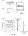
- FIG. 1is a generalized functional representation of an exemplary data storage device constructed and operated in accordance with various embodiments of the present invention.
- FIG. 2shows an exemplary construction for a resistive sense element (RSE) of the memory array of FIG. 1 in accordance with some embodiments.
- RSEresistive sense element
- FIGS. 3A-3Bshow respective erase and uni-directional writes of a memory cell of the device of FIG. 1 in accordance with various embodiments.
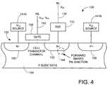
- FIG. 4is an elevational representation of the memory cell of FIGS. 3A-3B .
- FIGS. 5A-5Cshow a schematic representation of an array of memory cells from FIG. 4 subjected to respective single column erase, multi-column erase and multi-cell write operations.
- FIG. 6is a flow chart for a data access routine in accordance with various embodiments.
- FIG. 1provides a functional block representation of a data storage device 100 constructed and operated in accordance with various embodiments of the present invention.
- Top level control of the device 100 in FIG. 1is carried out by a controller 102 , which may be a programmable or hardware based microcontroller.
- the controller 102communicates with a host device via a controller interface (I/F) circuit 104 .
- a memory space 106comprises a number of memory arrays 108 .
- Each array 108comprises a block of semiconductor memory of selected storage capacity.
- the deviceis characterized as a solid-state drive (SSD).
- FIG. 2shows a resistive sense element (RSE) 110 used in various memory cells of the memory array 108 of FIG. 1 to store data.
- the RSE 110is characterized in FIG. 2 as a spin-torque transfer random access memory (STRAM), although other RSE constructions can be used.
- the STRAM RSEincludes a magnetic tunneling junction (MTJ) 112 with a fixed reference layer 114 , a free layer 116 and a tunneling barrier layer 118 .
- the MTJ 112is bounded by electrodes 120 , 122 .
- the electrodescomprise spin polarizing material that uniformly orients the spin of current passing through the RSE MTJ 112 .
- the reference layer 114has a fixed magnetic orientation in a selected direction. This fixed magnetic orientation can be established in a number of ways, such as via pinning to a separate magnet (not shown).
- the free layer 116has a selectively programmable magnetic orientation that can be parallel or anti-parallel with the selected direction of the reference layer 114 .
- Other respective magnetization orientationscan be used, such as orientations substantially perpendicular to those shown in FIG. 2 .
- a low resistance state R L for the MTJ 112is achieved when the magnetization of the free layer 116 is oriented to be substantially in the same direction (parallel) as the magnetization of the reference layer 114 .
- a write current 124passes through the MTJ 112 so that the magnetization direction of the reference layer 114 sets the magnetic orientation of the free layer 116 . Since electrons flow in the direction opposite to the direction of current, the write current direction passes from the free layer 116 to the reference layer 114 , and the electrons travel from the reference layer 114 to the free layer 116 .
- a high resistance state R H for the MTJ 112is established in the anti-parallel orientation in which the magnetization direction of the free layer 116 is substantially opposite that of the reference layer 114 .
- a write current 126passes through the MTJ 112 from the reference layer 114 to the free layer 116 so that spin-polarized electrons flow into the free layer 116 in the opposite direction.
- a different logical stateis assigned to each of the programmable resistances of the MTJ.
- the low resistance, parallel stateis used to represent a logical 1
- the high resistance, anti-parallel stateis used to represent a logical 1.
- Additional programmed statescan be used when the MTJ is configured to store multiple bits. For example, programmed resistances R 1 ⁇ R 2 ⁇ R 3 ⁇ R 4 can be used to respectively store multi-bit values “00,” “01,” “10” and “11”.
- RSEs such as 110can have asymmetric write characteristics in that it can require greater write effort to switch the programmed state in one direction as compared to another other direction.
- R H statecan require higher magnitudes of driving voltage and driving current as compared to the writing of the parallel low resistance R L state.
- the relative ordering of the RSE and a switching device within a memory cellcan contribute to asymmetric write characteristics, since the effective gate voltage may be lower when the direction of write current passes through the transistor prior to the RSE.
- various embodiments of the present inventionare generally directed to a memory cell comprising a switching device and a resistive sense element (RSE) having a hard programming direction and an easy programming direction.
- An erase operationis carried out to program the RSE in the hard programming direction by forward biasing a body-drain junction of the switching device.
- a write operationis carried out to program the RSE in the easy direction by applying a gate control voltage to the switching device and passing write current through a drain-source junction of the device.
- the memory cell configurationalso supports higher throughput block level read and write schemes, such as page-mode read and write operations.
- FIGS. 3A-3Bshows an exemplary memory cell 130 constructed and operated in accordance with various embodiments.
- the memory cell 130includes an RSE 110 connected in series with a switching device 132 .
- the RSE 110can be characterized as the MTJ 112 in FIG. 2 , although other RSE configurations can readily be used including but not limited to RRAM, MRAM, PCRAM and PMCs.
- the switching device 132can be characterized as a metal oxide semiconductor field effect transistor (MOSFET), although other switch configurations can be used including programmable elements.
- MOSFETmetal oxide semiconductor field effect transistor
- Support structures within the memory cell 110including an electrode layer 134 and a via 136 interconnect the RSE 110 and the switching device (transistor) 132 .
- a first control line 138characterized as a bit line BL is connected to an upper portion of the RSE 110 .
- a second control line 140characterized as a reference line, is set to a fixed control (reference) voltage V SS , such as ground or some other reference level via reference source 141 .
- the control line 140can take any number of suitable forms, such as a ground plane, in which case the reference source 141 can be characterized as a ground termination.
- the transistor 132includes respective drain, source and gate terminals.
- the drain terminalis connected to the RSE 110 as shown (by way of the via 136 and electrode 138 ).
- the source terminal of the transistor 132is connected to the reference voltage source 141 .
- the gate terminal of the transistor 132receives a gate control voltage input supplied by a word line WL 142 .
- Erase operations to write the RSE 110 to a first resistive state, such as logical 0,are shown in FIG. 3A .
- the erase operationsare carried out in the hard programming direction for the RSE 110 and can be initiated by setting the voltage V BL of the BL 138 to a level less than the fixed voltage V SS (V BL ⁇ V SS ), and by setting the WL 142 to the fixed reference voltage V SS .
- a body-drain diode junction 144 of the transistor 132When the V BL voltage is sufficiently low, a body-drain diode junction 144 of the transistor 132 will become forward biased and allow a first write (programming) current 146 to flow from the body of the transistor through the drain and to the RSE 110 .
- the body-drain PN junction 144is explicitly shown as a diode, but it will be understood that this is merely for purposes of illustration; the junction 144 is a characteristic of the transistor 142 and does not represent an additional diode circuit element.
- Write operations to write the RSE 110 to a second resistive state, such as logical 1,are shown in FIG. 3B .
- the write operationsare carried out in the easy programming direction for the RSE 110 and are initiated by applying a suitable gate control voltage, such as V DD to the word line WL 142 (V DD >V SS ) and setting the voltage VBL of the BL 138 to a level greater than the fixed voltage V SS (V BL >V SS ).
- V DDgate control voltage
- the second write current 148flows in the opposite direction through the RSE 110 as compared to the first write current 146 , and programs the RSE to a different resistive state. It is contemplated that the body-drain diode current 146 can potentially be larger than the normal source-drain current 148 of the transistor.
- the transistor 132can accordingly be sized to accommodate the lower current requirements of the second write current 148 , providing a smaller overall cell size and larger cell densities in a given semiconductor area.
- Driver circuitry and metallization processing to form separate conductors for the second control line 140can be eliminated, since the cell 130 is continuously maintained at the fixed reference voltage V SS during operation of the device.
- FIG. 4provides an exemplary elevational semiconductor layout of the memory cell 130 of FIGS. 3A-3B in accordance with some embodiments. Other layouts can readily be used.
- N+ doped regions 150 , 152are provided in a P substrate 154 to form respective source and drain regions of the cell transistor 132 .
- a control gate 156is coupled to the word line WL 142 and spans the source and drain regions 150 , 152 to selectively control transistor operation.
- the source region 150is permanently maintained at the V SS voltage via V SS source 141 A.
- the drain region 152is coupled to the RSE 110 as in FIGS. 3A-3B .
- a P+ contact region 158is formed in the substrate 154 to facilitate a permanent connection to a second VSS source 141 B (which may be the same source as 141 A).
- the forward biased PN junction 144 of FIG. 3Ais denoted in FIG. 4 along the boundary between the P material of the substrate 154 and the N+ drain region 152 .
- the erase current 146 in FIG. 3Apasses from the V SS source 141 B and through the P+ contact 158 , P substrate 154 and N+ drain region 152 to the RSE 110 . This body-drain current will flow while the voltage V BL is maintained below V SS and the gate 156 is maintained at V SS .
- the write current 148 of FIG. 3Bwill flow from the bit line BL 138 , through the RSE 110 to the N+ drain region 152 , across the cell transistor channel to the N+ source region 150 , and to the VSS source 141 A. This write current will flow responsive to V BL being greater than V SS , and the gate 156 being set to V DD .
- FIGS. 5A-5Cshow an array of memory cells 130 to illustrate various erase and write operations upon groups of cells.
- the memory cells 130can correspond to a selected array 108 from FIG. 1 , and are arranged into a series of rows and columns.
- the rowsare denoted 160 A- 160 C and the columns are denoted 162 A- 162 C. While a 3 ⁇ 3 array is shown, it will be appreciated that any respective numbers of rows and columns can be used to form an M ⁇ N memory block (such as 32 rows by 4096 columns, etc.).
- the cells 130 along each row 160 A- 160 Care connected to a common word line 142 (WL 1 -WL 3 ), and the cells 130 along each column 162 A- 162 C are connected to a common bit line 138 (BL 1 -BL 3 ).
- FIG. 5Aillustrates a single column erase operation.
- This configurationwill write each of the memory cells 130 in the selected column 162 C to the erased resistive state, in this case R L (logical 0).
- the programmed states of the memory cells 130 in the non-selected columns 162 A and 162 Bwill remain unaffected.
- the other columns 162 A, 162 Bcan be respectively erased in like manner.
- FIG. 5Bshows a multi-column erase operation.
- the bit lines BL 1 -BL 3 of all three columns 162 A- 162 Care set to the lower voltage V BL ⁇ V SS
- the word lines WL 1 -WL 3are set to the reference voltage V SS . This sets all of the memory cells 130 to the low resistive state (logical 0).
- FIG. 5Cshows a selective write operation in which selected memory cells 130 in the array 108 are written to a second resistive state, such as the high resistance R H (logical 1).
- the writing of logicalis in FIG. 5C can be carried out on an individual cell basis, to various cells along a selected row, or to various cells along a selected column.
- V BLV SS
- Cells along a selected columncan be similarly written by setting the associated bit line high and individually selecting the word lines for the cells to be written along the selected column.
- the data along a selected row or columncan be subsequently read in a number of ways.
- a page-mode operationis carried out in which read currents are applied by each of the bit lines to cells along a selected row.
- Sense amplifier circuitry(not shown) can sense the voltage drop across each memory cell along the selected row and latch an output state corresponding to the word data stored along the row.
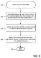
- FIG. 6provides a DATA ACCESS routine 200 generally illustrative of steps carried out in accordance with the foregoing discussion.
- an array of memory cellsis provided with each memory cell having an asymmetric RSE such as 110 and a switching device such as 132 .
- the memory cellsare arranged into rows and columns, with each memory cell connected between a first control line with a variable control voltage and a second control line (reference line) at a fixed reference voltage.
- a block of the memory cellsare erased by setting the memory cells to a first resistive state. In some embodiments, this is carried out by lowering the voltage of the associated first control lines below that of the fixed reference voltage, and flowing a body-drain junction current of the switching device through the associated RSE ( FIG. 3A ).
- step 206selected ones of the erased memory cells are subsequently written to a second resistive state, such as by raising the voltage of the first control lines of the selected memory cells to a voltage above that of the fixed reference voltage, and applying a gate control voltage to the switching device ( FIG. 3B ).
- the routinethen ends at step 208 .
- the source-drain current through the cell transistoris uni-directional because it is only used to write in a single direction, such as the low resistance parallel state of the exemplary MTJ 112 of FIG. 2 in the easy programming direction.
- the writing of the other state, such as the high resistance anti-parallel state of the MTJ 112 in FIG. 2uses the body-drain diode current, which can be a higher current consonant with the hard programming direction.
- the cell configuration embodied hereinfacilitates the use of higher spin-torque currents and/or the use of smaller devices. Also, the various embodiments herein allow connection of the source of an NMOSFET to be connected directly to the reference voltage VSS. This enables the use of smaller bit cells and eliminates the need for connections and drivers for an active source line SL since only two active signals connect to each cell (WL and BL). This can provide a more compact layout than prior art configurations.
- a block erase approach as embodied hereinalso allows a large number of cells to be simultaneously written to a selected resistive state (such as logical 0), allowing control circuitry to more closely conform to mature Flash memory control technologies. While STRAM MTJs have been embodied herein, it will be appreciated that the various embodiments can be adapted for any number of different types of RSE and switching device constructions.
Landscapes
- Engineering & Computer Science (AREA)
- Computer Hardware Design (AREA)
- Chemical & Material Sciences (AREA)
- Crystallography & Structural Chemistry (AREA)
- Mram Or Spin Memory Techniques (AREA)
- Semiconductor Memories (AREA)
Abstract
Description
Claims (18)
Priority Applications (6)
| Application Number | Priority Date | Filing Date | Title |
|---|---|---|---|
| US12/501,077US7885097B2 (en) | 2008-10-10 | 2009-07-10 | Non-volatile memory array with resistive sense element block erase and uni-directional write |
| PCT/US2010/041134WO2011005809A1 (en) | 2009-07-10 | 2010-07-07 | Non-volatile memory array with resistive sense element block erase and uni-directional write |
| JP2012519687AJP5688081B2 (en) | 2009-07-10 | 2010-07-07 | Nonvolatile memory array having resistance sensing elements for block erase and unidirectional writing |
| CN201080031900.2ACN102473448B (en) | 2009-07-10 | 2010-07-07 | Nonvolatile Memory Array with Resistive Sense Element Bulk Erase and Unidirectional Write |
| KR1020127003432AKR101361570B1 (en) | 2009-07-10 | 2010-07-07 | Non―volatile memory array with resistive sense element block erase and uni-directional write |
| US12/903,011US8213259B2 (en) | 2008-10-10 | 2010-10-12 | Non-volatile memory cell with resistive sense element block erase and uni-directional write |
Applications Claiming Priority (2)
| Application Number | Priority Date | Filing Date | Title |
|---|---|---|---|
| US10440208P | 2008-10-10 | 2008-10-10 | |
| US12/501,077US7885097B2 (en) | 2008-10-10 | 2009-07-10 | Non-volatile memory array with resistive sense element block erase and uni-directional write |
Related Child Applications (1)
| Application Number | Title | Priority Date | Filing Date |
|---|---|---|---|
| US12/903,011ContinuationUS8213259B2 (en) | 2008-10-10 | 2010-10-12 | Non-volatile memory cell with resistive sense element block erase and uni-directional write |
Publications (2)
| Publication Number | Publication Date |
|---|---|
| US20100091548A1 US20100091548A1 (en) | 2010-04-15 |
| US7885097B2true US7885097B2 (en) | 2011-02-08 |
Family
ID=47553700
Family Applications (2)
| Application Number | Title | Priority Date | Filing Date |
|---|---|---|---|
| US12/501,077Expired - Fee RelatedUS7885097B2 (en) | 2008-10-10 | 2009-07-10 | Non-volatile memory array with resistive sense element block erase and uni-directional write |
| US12/903,011Active2029-07-22US8213259B2 (en) | 2008-10-10 | 2010-10-12 | Non-volatile memory cell with resistive sense element block erase and uni-directional write |
Family Applications After (1)
| Application Number | Title | Priority Date | Filing Date |
|---|---|---|---|
| US12/903,011Active2029-07-22US8213259B2 (en) | 2008-10-10 | 2010-10-12 | Non-volatile memory cell with resistive sense element block erase and uni-directional write |
Country Status (1)
| Country | Link |
|---|---|
| US (2) | US7885097B2 (en) |
Cited By (1)
| Publication number | Priority date | Publication date | Assignee | Title |
|---|---|---|---|---|
| US20110026305A1 (en)* | 2008-10-10 | 2011-02-03 | Seagate Technology Llc | Non-Volatile Memory Array With Resistive Sense Element Block Erase and Uni-Directional Write |
Families Citing this family (11)
| Publication number | Priority date | Publication date | Assignee | Title |
|---|---|---|---|---|
| EP2685969A4 (en) | 2011-03-18 | 2014-08-06 | Catabasis Pharmaceuticals Inc | Use of intracellular enzymes for the release of covalently linked bioactives |
| US8730715B2 (en) | 2012-03-26 | 2014-05-20 | Honeywell International Inc. | Tamper-resistant MRAM utilizing chemical alteration |
| US9042164B2 (en) | 2012-03-26 | 2015-05-26 | Honeywell International Inc. | Anti-tampering devices and techniques for magnetoresistive random access memory |
| US8698517B2 (en)* | 2012-08-13 | 2014-04-15 | Globalfoundries Inc. | Computing multi-magnet based devices and methods for solution of optimization problems |
| US9349450B2 (en) | 2013-06-10 | 2016-05-24 | Micron Technology, Inc. | Memory devices and memory operational methods including single erase operation of conductive bridge memory cells |
| KR102127137B1 (en)* | 2013-12-03 | 2020-06-26 | 삼성전자주식회사 | Resistive memory device capable of increasing sensing margin by controlling interface state of cell transistors |
| US9269432B2 (en) | 2014-01-09 | 2016-02-23 | Micron Technology, Inc. | Memory systems and memory programming methods |
| US9336872B2 (en) | 2014-03-11 | 2016-05-10 | Everspin Technologies, Inc. | Nonvolatile logic and security circuits |
| US10043971B2 (en)* | 2014-11-18 | 2018-08-07 | Intel Corporation | Non-volatile register file including memory cells having conductive oxide memory element |
| US10395711B2 (en) | 2017-12-28 | 2019-08-27 | Spin Memory, Inc. | Perpendicular source and bit lines for an MRAM array |
| KR102663649B1 (en)* | 2018-09-14 | 2024-05-08 | 삼성전자주식회사 | Memory device configured to perform asymmetry write operation according to write direction |
Citations (19)
| Publication number | Priority date | Publication date | Assignee | Title |
|---|---|---|---|---|
| US6341085B1 (en) | 1991-11-26 | 2002-01-22 | Hitachi, Ltd. | Storage device employing a flash memory |
| US6617642B1 (en) | 2000-02-23 | 2003-09-09 | Tripath Technology, Inc. | Field effect transistor structure for driving inductive loads |
| US20040114438A1 (en)* | 2002-12-05 | 2004-06-17 | Sharp Kabushiki Kaisha | Semiconductor memory device and erase method for memory array |
| US6757842B2 (en) | 1989-04-13 | 2004-06-29 | Sandisk Corporation | Flash EEprom system |
| US6800897B2 (en) | 2001-04-11 | 2004-10-05 | Silicon Semiconductor Corporation | Integrated circuit power devices having junction barrier controlled schottky diodes therein |
| US20050122768A1 (en)* | 2003-09-12 | 2005-06-09 | Sharp Kabushiki Kaisha | Nonvolatile semiconductor memory device |
| US6940742B2 (en) | 2003-04-10 | 2005-09-06 | Seiko Epson Corporation | Method of storing data in ferroelectric memory device |
| US6944052B2 (en) | 2002-11-26 | 2005-09-13 | Freescale Semiconductor, Inc. | Magnetoresistive random access memory (MRAM) cell having a diode with asymmetrical characteristics |
| US20060044703A1 (en)* | 2002-12-13 | 2006-03-02 | Japan Science And Technology Agency | Spin injection device, magnetic device using the same, magnetic thin film used in the same |
| US7045840B2 (en) | 2003-12-04 | 2006-05-16 | Sharp Kabushiki Kaisha | Nonvolatile semiconductor memory device comprising a variable resistive element containing a perovskite-type crystal structure |
| US7180140B1 (en) | 2004-04-16 | 2007-02-20 | National Semiconductor Corporation | PMOS device with drain junction breakdown point located for reduced drain breakdown voltage walk-in and method for designing and manufacturing such device |
| WO2007100626A2 (en) | 2006-02-24 | 2007-09-07 | Grandis, Inc. | Current driven memory cells having enhanced current and enhanced current symmetry |
| US7272034B1 (en) | 2005-08-31 | 2007-09-18 | Grandis, Inc. | Current driven switching of magnetic storage cells utilizing spin transfer and magnetic memories using such cells |
| US20080007993A1 (en) | 2006-07-04 | 2008-01-10 | Sharp Kabushiki Kaisha | Semiconductor memory device |
| US7432574B2 (en) | 2006-03-29 | 2008-10-07 | Kabushiki Kaisha Toshiba | Magnetic recording element and magnetic memory |
| US7542356B2 (en) | 2006-11-01 | 2009-06-02 | Samsung Electronics Co., Ltd. | Semiconductor memory device and method for reducing cell activation during write operations |
| US20090161408A1 (en)* | 2006-12-08 | 2009-06-25 | Sharp Kabushiki Kaisha | Semiconductor memory device |
| US7646629B2 (en) | 2003-11-24 | 2010-01-12 | Thin Film Electronics Asa | Method for operating a data storage apparatus employing passive matrix addressing |
| US7732881B2 (en) | 2006-11-01 | 2010-06-08 | Avalanche Technology, Inc. | Current-confined effect of magnetic nano-current-channel (NCC) for magnetic random access memory (MRAM) |
Family Cites Families (5)
| Publication number | Priority date | Publication date | Assignee | Title |
|---|---|---|---|---|
| US3691535A (en)* | 1970-06-15 | 1972-09-12 | Sperry Rand Corp | Solid state memory array |
| JP3214715B2 (en)* | 1991-10-25 | 2001-10-02 | ローム株式会社 | Semiconductor storage element |
| JP2004145952A (en)* | 2002-10-23 | 2004-05-20 | Nec Electronics Corp | Mram and its writing method |
| US7898009B2 (en)* | 2007-02-22 | 2011-03-01 | American Semiconductor, Inc. | Independently-double-gated transistor memory (IDGM) |
| US7885097B2 (en)* | 2008-10-10 | 2011-02-08 | Seagate Technology Llc | Non-volatile memory array with resistive sense element block erase and uni-directional write |
- 2009
- 2009-07-10USUS12/501,077patent/US7885097B2/ennot_activeExpired - Fee Related
- 2010
- 2010-10-12USUS12/903,011patent/US8213259B2/enactiveActive
Patent Citations (21)
| Publication number | Priority date | Publication date | Assignee | Title |
|---|---|---|---|---|
| US7362618B2 (en) | 1989-04-13 | 2008-04-22 | Sandisk Corporation | Flash EEprom system |
| US6757842B2 (en) | 1989-04-13 | 2004-06-29 | Sandisk Corporation | Flash EEprom system |
| US7397713B2 (en) | 1989-04-13 | 2008-07-08 | Sandisk Corporation | Flash EEprom system |
| US6341085B1 (en) | 1991-11-26 | 2002-01-22 | Hitachi, Ltd. | Storage device employing a flash memory |
| US6617642B1 (en) | 2000-02-23 | 2003-09-09 | Tripath Technology, Inc. | Field effect transistor structure for driving inductive loads |
| US6800897B2 (en) | 2001-04-11 | 2004-10-05 | Silicon Semiconductor Corporation | Integrated circuit power devices having junction barrier controlled schottky diodes therein |
| US6944052B2 (en) | 2002-11-26 | 2005-09-13 | Freescale Semiconductor, Inc. | Magnetoresistive random access memory (MRAM) cell having a diode with asymmetrical characteristics |
| US20040114438A1 (en)* | 2002-12-05 | 2004-06-17 | Sharp Kabushiki Kaisha | Semiconductor memory device and erase method for memory array |
| US20060044703A1 (en)* | 2002-12-13 | 2006-03-02 | Japan Science And Technology Agency | Spin injection device, magnetic device using the same, magnetic thin film used in the same |
| US6940742B2 (en) | 2003-04-10 | 2005-09-06 | Seiko Epson Corporation | Method of storing data in ferroelectric memory device |
| US20050122768A1 (en)* | 2003-09-12 | 2005-06-09 | Sharp Kabushiki Kaisha | Nonvolatile semiconductor memory device |
| US7646629B2 (en) | 2003-11-24 | 2010-01-12 | Thin Film Electronics Asa | Method for operating a data storage apparatus employing passive matrix addressing |
| US7045840B2 (en) | 2003-12-04 | 2006-05-16 | Sharp Kabushiki Kaisha | Nonvolatile semiconductor memory device comprising a variable resistive element containing a perovskite-type crystal structure |
| US7180140B1 (en) | 2004-04-16 | 2007-02-20 | National Semiconductor Corporation | PMOS device with drain junction breakdown point located for reduced drain breakdown voltage walk-in and method for designing and manufacturing such device |
| US7272034B1 (en) | 2005-08-31 | 2007-09-18 | Grandis, Inc. | Current driven switching of magnetic storage cells utilizing spin transfer and magnetic memories using such cells |
| WO2007100626A2 (en) | 2006-02-24 | 2007-09-07 | Grandis, Inc. | Current driven memory cells having enhanced current and enhanced current symmetry |
| US7432574B2 (en) | 2006-03-29 | 2008-10-07 | Kabushiki Kaisha Toshiba | Magnetic recording element and magnetic memory |
| US20080007993A1 (en) | 2006-07-04 | 2008-01-10 | Sharp Kabushiki Kaisha | Semiconductor memory device |
| US7542356B2 (en) | 2006-11-01 | 2009-06-02 | Samsung Electronics Co., Ltd. | Semiconductor memory device and method for reducing cell activation during write operations |
| US7732881B2 (en) | 2006-11-01 | 2010-06-08 | Avalanche Technology, Inc. | Current-confined effect of magnetic nano-current-channel (NCC) for magnetic random access memory (MRAM) |
| US20090161408A1 (en)* | 2006-12-08 | 2009-06-25 | Sharp Kabushiki Kaisha | Semiconductor memory device |
Non-Patent Citations (1)
| Title |
|---|
| PCT/ISA/210 International Search Report and PCT/ISA/237 Written Opinion for PCT/US2010/041134 from the EPO. |
Cited By (2)
| Publication number | Priority date | Publication date | Assignee | Title |
|---|---|---|---|---|
| US20110026305A1 (en)* | 2008-10-10 | 2011-02-03 | Seagate Technology Llc | Non-Volatile Memory Array With Resistive Sense Element Block Erase and Uni-Directional Write |
| US8213259B2 (en)* | 2008-10-10 | 2012-07-03 | Seagate Technology Llc | Non-volatile memory cell with resistive sense element block erase and uni-directional write |
Also Published As
| Publication number | Publication date |
|---|---|
| US20100091548A1 (en) | 2010-04-15 |
| US8213259B2 (en) | 2012-07-03 |
| US20110026305A1 (en) | 2011-02-03 |
Similar Documents
| Publication | Publication Date | Title |
|---|---|---|
| US7885097B2 (en) | Non-volatile memory array with resistive sense element block erase and uni-directional write | |
| US7933136B2 (en) | Non-volatile memory cell with multiple resistive sense elements sharing a common switching device | |
| US8422271B2 (en) | Bidirectional non-volatile memory array architecture | |
| US7974121B2 (en) | Write current compensation using word line boosting circuitry | |
| US8107282B2 (en) | Asymmetric write current compensation | |
| US7830693B2 (en) | NAND based resistive sense memory cell architecture | |
| KR101402205B1 (en) | Hierarchical cross-point array of non-volatile memory | |
| US20110299323A1 (en) | Floating Source Line Architecture for Non-Volatile Memory | |
| US6791867B2 (en) | Selection of memory cells in data storage devices | |
| US8004875B2 (en) | Current magnitude compensation for memory cells in a data storage array | |
| KR101361570B1 (en) | Non―volatile memory array with resistive sense element block erase and uni-directional write | |
| US8804408B2 (en) | Semiconductor storage device | |
| US8830734B2 (en) | Using a nearby cell to provide field assisted switching in a magnetic memory array | |
| JP5688081B2 (en) | Nonvolatile memory array having resistance sensing elements for block erase and unidirectional writing | |
| US8363450B2 (en) | Hierarchical cross-point array of non-volatile memory | |
| US12424257B2 (en) | Memory devices with dual-side access circuits and methods for operating the same |
Legal Events
| Date | Code | Title | Description |
|---|---|---|---|
| AS | Assignment | Owner name:SEAGATE TECHNOLOGY LLC,CALIFORNIA Free format text:ASSIGNMENT OF ASSIGNORS INTEREST;ASSIGNORS:REED, DANIEL S.;LU, YONG;LI, HAI;SIGNING DATES FROM 20090706 TO 20090707;REEL/FRAME:022941/0858 Owner name:SEAGATE TECHNOLOGY LLC, CALIFORNIA Free format text:ASSIGNMENT OF ASSIGNORS INTEREST;ASSIGNORS:REED, DANIEL S.;LU, YONG;LI, HAI;SIGNING DATES FROM 20090706 TO 20090707;REEL/FRAME:022941/0858 | |
| STCF | Information on status: patent grant | Free format text:PATENTED CASE | |
| AS | Assignment | Owner name:THE BANK OF NOVA SCOTIA, AS ADMINISTRATIVE AGENT, CANADA Free format text:SECURITY AGREEMENT;ASSIGNOR:SEAGATE TECHNOLOGY LLC;REEL/FRAME:026010/0350 Effective date:20110118 Owner name:THE BANK OF NOVA SCOTIA, AS ADMINISTRATIVE AGENT, Free format text:SECURITY AGREEMENT;ASSIGNOR:SEAGATE TECHNOLOGY LLC;REEL/FRAME:026010/0350 Effective date:20110118 | |
| FPAY | Fee payment | Year of fee payment:4 | |
| FEPP | Fee payment procedure | Free format text:MAINTENANCE FEE REMINDER MAILED (ORIGINAL EVENT CODE: REM.); ENTITY STATUS OF PATENT OWNER: LARGE ENTITY | |
| FEPP | Fee payment procedure | Free format text:7.5 YR SURCHARGE - LATE PMT W/IN 6 MO, LARGE ENTITY (ORIGINAL EVENT CODE: M1555); ENTITY STATUS OF PATENT OWNER: LARGE ENTITY | |
| MAFP | Maintenance fee payment | Free format text:PAYMENT OF MAINTENANCE FEE, 8TH YEAR, LARGE ENTITY (ORIGINAL EVENT CODE: M1552); ENTITY STATUS OF PATENT OWNER: LARGE ENTITY Year of fee payment:8 | |
| FEPP | Fee payment procedure | Free format text:MAINTENANCE FEE REMINDER MAILED (ORIGINAL EVENT CODE: REM.); ENTITY STATUS OF PATENT OWNER: LARGE ENTITY | |
| LAPS | Lapse for failure to pay maintenance fees | Free format text:PATENT EXPIRED FOR FAILURE TO PAY MAINTENANCE FEES (ORIGINAL EVENT CODE: EXP.); ENTITY STATUS OF PATENT OWNER: LARGE ENTITY | |
| STCH | Information on status: patent discontinuation | Free format text:PATENT EXPIRED DUE TO NONPAYMENT OF MAINTENANCE FEES UNDER 37 CFR 1.362 | |
| FP | Lapsed due to failure to pay maintenance fee | Effective date:20230208 | |
| AS | Assignment | Owner name:SEAGATE TECHNOLOGY PUBLIC LIMITED COMPANY, CALIFORNIA Free format text:RELEASE BY SECURED PARTY;ASSIGNOR:THE BANK OF NOVA SCOTIA;REEL/FRAME:072193/0001 Effective date:20250303 Owner name:SEAGATE TECHNOLOGY, CALIFORNIA Free format text:RELEASE BY SECURED PARTY;ASSIGNOR:THE BANK OF NOVA SCOTIA;REEL/FRAME:072193/0001 Effective date:20250303 Owner name:SEAGATE TECHNOLOGY HDD HOLDINGS, CALIFORNIA Free format text:RELEASE BY SECURED PARTY;ASSIGNOR:THE BANK OF NOVA SCOTIA;REEL/FRAME:072193/0001 Effective date:20250303 Owner name:I365 INC., CALIFORNIA Free format text:RELEASE BY SECURED PARTY;ASSIGNOR:THE BANK OF NOVA SCOTIA;REEL/FRAME:072193/0001 Effective date:20250303 Owner name:SEAGATE TECHNOLOGY LLC, CALIFORNIA Free format text:RELEASE BY SECURED PARTY;ASSIGNOR:THE BANK OF NOVA SCOTIA;REEL/FRAME:072193/0001 Effective date:20250303 Owner name:SEAGATE TECHNOLOGY INTERNATIONAL, CAYMAN ISLANDS Free format text:RELEASE BY SECURED PARTY;ASSIGNOR:THE BANK OF NOVA SCOTIA;REEL/FRAME:072193/0001 Effective date:20250303 Owner name:SEAGATE HDD CAYMAN, CAYMAN ISLANDS Free format text:RELEASE BY SECURED PARTY;ASSIGNOR:THE BANK OF NOVA SCOTIA;REEL/FRAME:072193/0001 Effective date:20250303 Owner name:SEAGATE TECHNOLOGY (US) HOLDINGS, INC., CALIFORNIA Free format text:RELEASE BY SECURED PARTY;ASSIGNOR:THE BANK OF NOVA SCOTIA;REEL/FRAME:072193/0001 Effective date:20250303 |