US7884394B2 - III-nitride devices and circuits - Google Patents
III-nitride devices and circuitsDownload PDFInfo
- Publication number
- US7884394B2 US7884394B2US12/368,248US36824809AUS7884394B2US 7884394 B2US7884394 B2US 7884394B2US 36824809 AUS36824809 AUS 36824809AUS 7884394 B2US7884394 B2US 7884394B2
- Authority
- US
- United States
- Prior art keywords
- transistor
- iii
- layers
- gate
- mode transistor
- Prior art date
- Legal status (The legal status is an assumption and is not a legal conclusion. Google has not performed a legal analysis and makes no representation as to the accuracy of the status listed.)
- Active, expires
Links
Images


Classifications
- H—ELECTRICITY
- H10—SEMICONDUCTOR DEVICES; ELECTRIC SOLID-STATE DEVICES NOT OTHERWISE PROVIDED FOR
- H10D—INORGANIC ELECTRIC SEMICONDUCTOR DEVICES
- H10D30/00—Field-effect transistors [FET]
- H10D30/40—FETs having zero-dimensional [0D], one-dimensional [1D] or two-dimensional [2D] charge carrier gas channels
- H10D30/47—FETs having zero-dimensional [0D], one-dimensional [1D] or two-dimensional [2D] charge carrier gas channels having 2D charge carrier gas channels, e.g. nanoribbon FETs or high electron mobility transistors [HEMT]
- H10D30/471—High electron mobility transistors [HEMT] or high hole mobility transistors [HHMT]
- H10D30/475—High electron mobility transistors [HEMT] or high hole mobility transistors [HHMT] having wider bandgap layer formed on top of lower bandgap active layer, e.g. undoped barrier HEMTs such as i-AlGaN/GaN HEMTs
- H—ELECTRICITY
- H01—ELECTRIC ELEMENTS
- H01L—SEMICONDUCTOR DEVICES NOT COVERED BY CLASS H10
- H01L23/00—Details of semiconductor or other solid state devices
- H01L23/48—Arrangements for conducting electric current to or from the solid state body in operation, e.g. leads, terminal arrangements ; Selection of materials therefor
- H01L23/488—Arrangements for conducting electric current to or from the solid state body in operation, e.g. leads, terminal arrangements ; Selection of materials therefor consisting of soldered or bonded constructions
- H01L23/492—Bases or plates or solder therefor
- H—ELECTRICITY
- H01—ELECTRIC ELEMENTS
- H01L—SEMICONDUCTOR DEVICES NOT COVERED BY CLASS H10
- H01L25/00—Assemblies consisting of a plurality of semiconductor or other solid state devices
- H01L25/03—Assemblies consisting of a plurality of semiconductor or other solid state devices all the devices being of a type provided for in a single subclass of subclasses H10B, H10D, H10F, H10H, H10K or H10N, e.g. assemblies of rectifier diodes
- H01L25/04—Assemblies consisting of a plurality of semiconductor or other solid state devices all the devices being of a type provided for in a single subclass of subclasses H10B, H10D, H10F, H10H, H10K or H10N, e.g. assemblies of rectifier diodes the devices not having separate containers
- H01L25/07—Assemblies consisting of a plurality of semiconductor or other solid state devices all the devices being of a type provided for in a single subclass of subclasses H10B, H10D, H10F, H10H, H10K or H10N, e.g. assemblies of rectifier diodes the devices not having separate containers the devices being of a type provided for in group subclass H10D
- H01L25/072—Assemblies consisting of a plurality of semiconductor or other solid state devices all the devices being of a type provided for in a single subclass of subclasses H10B, H10D, H10F, H10H, H10K or H10N, e.g. assemblies of rectifier diodes the devices not having separate containers the devices being of a type provided for in group subclass H10D the devices being arranged next to each other
- H—ELECTRICITY
- H10—SEMICONDUCTOR DEVICES; ELECTRIC SOLID-STATE DEVICES NOT OTHERWISE PROVIDED FOR
- H10D—INORGANIC ELECTRIC SEMICONDUCTOR DEVICES
- H10D64/00—Electrodes of devices having potential barriers
- H10D64/111—Field plates
- H—ELECTRICITY
- H01—ELECTRIC ELEMENTS
- H01L—SEMICONDUCTOR DEVICES NOT COVERED BY CLASS H10
- H01L2224/00—Indexing scheme for arrangements for connecting or disconnecting semiconductor or solid-state bodies and methods related thereto as covered by H01L24/00
- H01L2224/01—Means for bonding being attached to, or being formed on, the surface to be connected, e.g. chip-to-package, die-attach, "first-level" interconnects; Manufacturing methods related thereto
- H01L2224/26—Layer connectors, e.g. plate connectors, solder or adhesive layers; Manufacturing methods related thereto
- H01L2224/28—Structure, shape, material or disposition of the layer connectors prior to the connecting process
- H01L2224/29—Structure, shape, material or disposition of the layer connectors prior to the connecting process of an individual layer connector
- H01L2224/29001—Core members of the layer connector
- H01L2224/29099—Material
- H01L2224/291—Material with a principal constituent of the material being a metal or a metalloid, e.g. boron [B], silicon [Si], germanium [Ge], arsenic [As], antimony [Sb], tellurium [Te] and polonium [Po], and alloys thereof
- H—ELECTRICITY
- H01—ELECTRIC ELEMENTS
- H01L—SEMICONDUCTOR DEVICES NOT COVERED BY CLASS H10
- H01L2224/00—Indexing scheme for arrangements for connecting or disconnecting semiconductor or solid-state bodies and methods related thereto as covered by H01L24/00
- H01L2224/01—Means for bonding being attached to, or being formed on, the surface to be connected, e.g. chip-to-package, die-attach, "first-level" interconnects; Manufacturing methods related thereto
- H01L2224/26—Layer connectors, e.g. plate connectors, solder or adhesive layers; Manufacturing methods related thereto
- H01L2224/28—Structure, shape, material or disposition of the layer connectors prior to the connecting process
- H01L2224/29—Structure, shape, material or disposition of the layer connectors prior to the connecting process of an individual layer connector
- H01L2224/29001—Core members of the layer connector
- H01L2224/29099—Material
- H01L2224/2919—Material with a principal constituent of the material being a polymer, e.g. polyester, phenolic based polymer, epoxy
- H—ELECTRICITY
- H01—ELECTRIC ELEMENTS
- H01L—SEMICONDUCTOR DEVICES NOT COVERED BY CLASS H10
- H01L2224/00—Indexing scheme for arrangements for connecting or disconnecting semiconductor or solid-state bodies and methods related thereto as covered by H01L24/00
- H01L2224/01—Means for bonding being attached to, or being formed on, the surface to be connected, e.g. chip-to-package, die-attach, "first-level" interconnects; Manufacturing methods related thereto
- H01L2224/42—Wire connectors; Manufacturing methods related thereto
- H01L2224/47—Structure, shape, material or disposition of the wire connectors after the connecting process
- H01L2224/48—Structure, shape, material or disposition of the wire connectors after the connecting process of an individual wire connector
- H01L2224/481—Disposition
- H01L2224/48135—Connecting between different semiconductor or solid-state bodies, i.e. chip-to-chip
- H01L2224/48137—Connecting between different semiconductor or solid-state bodies, i.e. chip-to-chip the bodies being arranged next to each other, e.g. on a common substrate
- H—ELECTRICITY
- H01—ELECTRIC ELEMENTS
- H01L—SEMICONDUCTOR DEVICES NOT COVERED BY CLASS H10
- H01L2224/00—Indexing scheme for arrangements for connecting or disconnecting semiconductor or solid-state bodies and methods related thereto as covered by H01L24/00
- H01L2224/01—Means for bonding being attached to, or being formed on, the surface to be connected, e.g. chip-to-package, die-attach, "first-level" interconnects; Manufacturing methods related thereto
- H01L2224/42—Wire connectors; Manufacturing methods related thereto
- H01L2224/47—Structure, shape, material or disposition of the wire connectors after the connecting process
- H01L2224/48—Structure, shape, material or disposition of the wire connectors after the connecting process of an individual wire connector
- H01L2224/481—Disposition
- H01L2224/48151—Connecting between a semiconductor or solid-state body and an item not being a semiconductor or solid-state body, e.g. chip-to-substrate, chip-to-passive
- H01L2224/48221—Connecting between a semiconductor or solid-state body and an item not being a semiconductor or solid-state body, e.g. chip-to-substrate, chip-to-passive the body and the item being stacked
- H01L2224/48245—Connecting between a semiconductor or solid-state body and an item not being a semiconductor or solid-state body, e.g. chip-to-substrate, chip-to-passive the body and the item being stacked the item being metallic
- H01L2224/48257—Connecting between a semiconductor or solid-state body and an item not being a semiconductor or solid-state body, e.g. chip-to-substrate, chip-to-passive the body and the item being stacked the item being metallic connecting the wire to a die pad of the item
- H—ELECTRICITY
- H01—ELECTRIC ELEMENTS
- H01L—SEMICONDUCTOR DEVICES NOT COVERED BY CLASS H10
- H01L2224/00—Indexing scheme for arrangements for connecting or disconnecting semiconductor or solid-state bodies and methods related thereto as covered by H01L24/00
- H01L2224/01—Means for bonding being attached to, or being formed on, the surface to be connected, e.g. chip-to-package, die-attach, "first-level" interconnects; Manufacturing methods related thereto
- H01L2224/42—Wire connectors; Manufacturing methods related thereto
- H01L2224/47—Structure, shape, material or disposition of the wire connectors after the connecting process
- H01L2224/49—Structure, shape, material or disposition of the wire connectors after the connecting process of a plurality of wire connectors
- H01L2224/491—Disposition
- H01L2224/4911—Disposition the connectors being bonded to at least one common bonding area, e.g. daisy chain
- H01L2224/49111—Disposition the connectors being bonded to at least one common bonding area, e.g. daisy chain the connectors connecting two common bonding areas, e.g. Litz or braid wires
- H—ELECTRICITY
- H01—ELECTRIC ELEMENTS
- H01L—SEMICONDUCTOR DEVICES NOT COVERED BY CLASS H10
- H01L2224/00—Indexing scheme for arrangements for connecting or disconnecting semiconductor or solid-state bodies and methods related thereto as covered by H01L24/00
- H01L2224/01—Means for bonding being attached to, or being formed on, the surface to be connected, e.g. chip-to-package, die-attach, "first-level" interconnects; Manufacturing methods related thereto
- H01L2224/42—Wire connectors; Manufacturing methods related thereto
- H01L2224/47—Structure, shape, material or disposition of the wire connectors after the connecting process
- H01L2224/49—Structure, shape, material or disposition of the wire connectors after the connecting process of a plurality of wire connectors
- H01L2224/491—Disposition
- H01L2224/4912—Layout
- H01L2224/4917—Crossed wires
- H—ELECTRICITY
- H01—ELECTRIC ELEMENTS
- H01L—SEMICONDUCTOR DEVICES NOT COVERED BY CLASS H10
- H01L2224/00—Indexing scheme for arrangements for connecting or disconnecting semiconductor or solid-state bodies and methods related thereto as covered by H01L24/00
- H01L2224/01—Means for bonding being attached to, or being formed on, the surface to be connected, e.g. chip-to-package, die-attach, "first-level" interconnects; Manufacturing methods related thereto
- H01L2224/42—Wire connectors; Manufacturing methods related thereto
- H01L2224/47—Structure, shape, material or disposition of the wire connectors after the connecting process
- H01L2224/49—Structure, shape, material or disposition of the wire connectors after the connecting process of a plurality of wire connectors
- H01L2224/491—Disposition
- H01L2224/4912—Layout
- H01L2224/49175—Parallel arrangements
- H—ELECTRICITY
- H01—ELECTRIC ELEMENTS
- H01L—SEMICONDUCTOR DEVICES NOT COVERED BY CLASS H10
- H01L2224/00—Indexing scheme for arrangements for connecting or disconnecting semiconductor or solid-state bodies and methods related thereto as covered by H01L24/00
- H01L2224/73—Means for bonding being of different types provided for in two or more of groups H01L2224/10, H01L2224/18, H01L2224/26, H01L2224/34, H01L2224/42, H01L2224/50, H01L2224/63, H01L2224/71
- H01L2224/732—Location after the connecting process
- H01L2224/73251—Location after the connecting process on different surfaces
- H01L2224/73265—Layer and wire connectors
- H—ELECTRICITY
- H01—ELECTRIC ELEMENTS
- H01L—SEMICONDUCTOR DEVICES NOT COVERED BY CLASS H10
- H01L24/00—Arrangements for connecting or disconnecting semiconductor or solid-state bodies; Methods or apparatus related thereto
- H01L24/01—Means for bonding being attached to, or being formed on, the surface to be connected, e.g. chip-to-package, die-attach, "first-level" interconnects; Manufacturing methods related thereto
- H01L24/42—Wire connectors; Manufacturing methods related thereto
- H01L24/47—Structure, shape, material or disposition of the wire connectors after the connecting process
- H01L24/48—Structure, shape, material or disposition of the wire connectors after the connecting process of an individual wire connector
- H—ELECTRICITY
- H01—ELECTRIC ELEMENTS
- H01L—SEMICONDUCTOR DEVICES NOT COVERED BY CLASS H10
- H01L24/00—Arrangements for connecting or disconnecting semiconductor or solid-state bodies; Methods or apparatus related thereto
- H01L24/01—Means for bonding being attached to, or being formed on, the surface to be connected, e.g. chip-to-package, die-attach, "first-level" interconnects; Manufacturing methods related thereto
- H01L24/42—Wire connectors; Manufacturing methods related thereto
- H01L24/47—Structure, shape, material or disposition of the wire connectors after the connecting process
- H01L24/49—Structure, shape, material or disposition of the wire connectors after the connecting process of a plurality of wire connectors
- H—ELECTRICITY
- H01—ELECTRIC ELEMENTS
- H01L—SEMICONDUCTOR DEVICES NOT COVERED BY CLASS H10
- H01L25/00—Assemblies consisting of a plurality of semiconductor or other solid state devices
- H01L25/18—Assemblies consisting of a plurality of semiconductor or other solid state devices the devices being of the types provided for in two or more different main groups of the same subclass of H10B, H10D, H10F, H10H, H10K or H10N
- H—ELECTRICITY
- H01—ELECTRIC ELEMENTS
- H01L—SEMICONDUCTOR DEVICES NOT COVERED BY CLASS H10
- H01L2924/00—Indexing scheme for arrangements or methods for connecting or disconnecting semiconductor or solid-state bodies as covered by H01L24/00
- H01L2924/0001—Technical content checked by a classifier
- H01L2924/00014—Technical content checked by a classifier the subject-matter covered by the group, the symbol of which is combined with the symbol of this group, being disclosed without further technical details
- H—ELECTRICITY
- H01—ELECTRIC ELEMENTS
- H01L—SEMICONDUCTOR DEVICES NOT COVERED BY CLASS H10
- H01L2924/00—Indexing scheme for arrangements or methods for connecting or disconnecting semiconductor or solid-state bodies as covered by H01L24/00
- H01L2924/01—Chemical elements
- H01L2924/01068—Erbium [Er]
- H—ELECTRICITY
- H01—ELECTRIC ELEMENTS
- H01L—SEMICONDUCTOR DEVICES NOT COVERED BY CLASS H10
- H01L2924/00—Indexing scheme for arrangements or methods for connecting or disconnecting semiconductor or solid-state bodies as covered by H01L24/00
- H01L2924/01—Chemical elements
- H01L2924/01079—Gold [Au]
- H—ELECTRICITY
- H01—ELECTRIC ELEMENTS
- H01L—SEMICONDUCTOR DEVICES NOT COVERED BY CLASS H10
- H01L2924/00—Indexing scheme for arrangements or methods for connecting or disconnecting semiconductor or solid-state bodies as covered by H01L24/00
- H01L2924/10—Details of semiconductor or other solid state devices to be connected
- H01L2924/11—Device type
- H01L2924/12—Passive devices, e.g. 2 terminal devices
- H01L2924/1203—Rectifying Diode
- H01L2924/12036—PN diode
- H—ELECTRICITY
- H01—ELECTRIC ELEMENTS
- H01L—SEMICONDUCTOR DEVICES NOT COVERED BY CLASS H10
- H01L2924/00—Indexing scheme for arrangements or methods for connecting or disconnecting semiconductor or solid-state bodies as covered by H01L24/00
- H01L2924/10—Details of semiconductor or other solid state devices to be connected
- H01L2924/11—Device type
- H01L2924/13—Discrete devices, e.g. 3 terminal devices
- H01L2924/1304—Transistor
- H01L2924/1305—Bipolar Junction Transistor [BJT]
- H01L2924/13055—Insulated gate bipolar transistor [IGBT]
- H—ELECTRICITY
- H01—ELECTRIC ELEMENTS
- H01L—SEMICONDUCTOR DEVICES NOT COVERED BY CLASS H10
- H01L2924/00—Indexing scheme for arrangements or methods for connecting or disconnecting semiconductor or solid-state bodies as covered by H01L24/00
- H01L2924/10—Details of semiconductor or other solid state devices to be connected
- H01L2924/11—Device type
- H01L2924/13—Discrete devices, e.g. 3 terminal devices
- H01L2924/1304—Transistor
- H01L2924/1306—Field-effect transistor [FET]
- H01L2924/13091—Metal-Oxide-Semiconductor Field-Effect Transistor [MOSFET]
- H—ELECTRICITY
- H01—ELECTRIC ELEMENTS
- H01L—SEMICONDUCTOR DEVICES NOT COVERED BY CLASS H10
- H01L2924/00—Indexing scheme for arrangements or methods for connecting or disconnecting semiconductor or solid-state bodies as covered by H01L24/00
- H01L2924/19—Details of hybrid assemblies other than the semiconductor or other solid state devices to be connected
- H01L2924/191—Disposition
- H01L2924/19101—Disposition of discrete passive components
- H01L2924/19107—Disposition of discrete passive components off-chip wires
- H—ELECTRICITY
- H10—SEMICONDUCTOR DEVICES; ELECTRIC SOLID-STATE DEVICES NOT OTHERWISE PROVIDED FOR
- H10D—INORGANIC ELECTRIC SEMICONDUCTOR DEVICES
- H10D62/00—Semiconductor bodies, or regions thereof, of devices having potential barriers
- H10D62/80—Semiconductor bodies, or regions thereof, of devices having potential barriers characterised by the materials
- H10D62/85—Semiconductor bodies, or regions thereof, of devices having potential barriers characterised by the materials being Group III-V materials, e.g. GaAs
- H10D62/8503—Nitride Group III-V materials, e.g. AlN or GaN
Definitions
- This inventionrelates to semiconductor electronic devices, specifically III-Nitride HEMT devices with field plates, and circuits which they comprise.
- III-Nitride (III-N) semiconductor devicesare now emerging as an attractive candidate to carry large currents and support high voltages, providing very low on resistance, high voltage device operation, and fast switching times.
- HEMThigh electron mobility transistor
- FIG. 1A typical III-N high electron mobility transistor (HEMT), shown in FIG. 1 , comprises a substrate 10 , a channel layer 11 , such as GaN, atop the substrate, and a barrier layer 12 , such as Al x Ga 1-x N, atop the channel layer.
- a two-dimensional electron gas (2DEG) channel 19is induced in the channel layer 11 near the interface between the channel layer 11 and the barrier layer 12 .
- Source and drain electrodes 14 and 15respectively, form ohmic contacts to the 2DEG
- Gate electrode 16modulates the portion of the 2DEG in the gate region, i.e., directly beneath gate electrode 16 .
- Field platesare commonly used in III-N devices to shape the electric field in the high-field region of the device in such a way that reduces the peak field and increases the device breakdown voltage, thereby allowing for higher voltage operation.
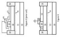
- Examples of field plated III-N HEMTsare shown in FIGS. 2 and 3 .
- the device in FIG. 2includes a field plate 18 which is connected to gate electrode 16 , i.e., a gate-connected field plate, and an insulator layer 13 , such as a layer of SiN, is between the field plate and the barrier layer 12 .
- Field plate 18can include or be formed of the same material as gate electrode 16 .
- the manufacturing process for a device with a gate-connected field plateis typically relatively simple as compared to that for devices with different field plate configurations, since there is no need to form separate field plate and gate electrode layers, thus the deposition of the gate electrode and field plate can be performed in a single processing step.
- the gate-connected field plate 18 in FIG. 2increases the capacitance between the gate 16 and drain electrodes 15 , thereby reducing the effective operating speed of the device. This increase in capacitance between the input and output of the device, along with the corresponding reduction in high frequency response, is known as the Miller capacitance effect or Miller effect.
- the source electrode 14is typically grounded, as indicated in the figure.
- the field plate 18is connected to the source electrode 14 , i.e. field plate 18 is a source-connected field plate. Connecting the field plate to the source electrode can reduce or eliminate the Miller effect, since the voltage on the field plate remains fixed when an input signal is applied to the gate electrode. For this configuration, the capacitance between input and output is the source-to-drain capacitance, which typically is small and therefore has a negligible impact on device performance.
- the manufacturing process for this deviceis more complicated than that for devices with gate-connected field plates, such as the device of FIG. 2 .
- a III-N based high electron mobility transistorHEMT
- the transistorhas a series of III-N layers, which form a 2DEG channel, a gate electrode on a first side of the series of III-N layers in a gate region, a field plate electrically connected to the gate electrode and separated from the III-N layers by an electrical insulator and a ground connection electrically connected to the field plate and the gate electrode, forming a gate-connected grounded field plate.
- the transistors that are described hereincan be operated by biasing a source electrode of the transistor and the gate electrode of the transistor, wherein during biasing capacitance between an input and an output of the transistor is minimized in comparison with a similar transistor lacking the gate-connected grounded field plate.
- a circuitcan include one of the transistors described herein and that is a depletion mode transistor, along with a low voltage enhancement mode transistor, wherein the source of the depletion mode transistor is electrically connected to a drain of the enhancement mode transistor.
- An assemblycan include one of the circuits that are described herein with a substrate.
- the substrateincludes a conductive layer as the ground connection.
- the depletion mode transistor and the enhancement mode transistorare attached to the substrate and a source electrode of the enhancement mode transistor is electrically connected to the ground connection.
- circuitscan include a transistor that is described herein along with a diode.
- the source of the transistoris electrically connected to a cathode of the diode.
- the series of III-N layerscan include at least three III-N layers, each of the three III-N layers having a different composition. At least one of the layers can be AlN.
- the 2DEG channelcan be a first 2DEG channel
- the series of III-N layerscan form the first 2DEG channel in a channel III-N layer of the series of III-N layers
- a second 2DEG channelcan be in the series of III-N layers and parallel to the first 2DEG channel.
- An insulating layercan be between the gate electrode and the series of III-N layers.
- a gate recesscan be in the series of III-N layers in the gate region and at least a portion of the gate electrode lies within the gate recess.
- the field platecan have multiple portions that are each a different distance away from the series of III-N layers.
- the ground connectioncan be an electrically conductive layer that has a lateral expanse that is greater than a lateral expanse of the transistor.
- the field platecan be a slant field plate.
- the transistorcan be a depletion mode transistor.
- a source of the enhancement mode transistorcan be grounded.
- the enhancement mode transistorcan be a vertical device and the depletion mode transistor can be a lateral device.
- An insulating layercan be between the enhancement mode transistor and the substrate, the insulating layer electrically isolating the enhancement mode transistor from the substrate.
- the enhancement mode transistorcan be a vertical device with a gate electrode and the drain electrode on one side of a series of layers of the transistor and a source electrode on an opposite side of the series of layers and the source electrode of the enhancement mode transistor can be mounted directly on the ground connection of the substrate.
- An assemblycan include a source lead, a gate lead and a drain lead on the substrate.
- the source leadcan be electrically connected to the conductive layer of the substrate.
- the gate leadcan be electrically connected to the gate electrode of the enhancement mode transistor and electrically insulated from the conductive layer of the substrate.
- the drain leadcan be electrically connected to the drain electrode of the depletion mode transistor and electrically insulated from the conductive layer of the substrate.
- the circuitcan include a diode, wherein an anode of the diode is electrically connected to the drain of the depletion mode transistor.
- the diode, the enhancement mode transistor and the depletion mode transistorcan be on a common substrate and the diode can include III-N materials.
- An anode of the diodecan be electrically connected to the ground connection.
- the diode and the transistorare on a common substrate and the diode can comprise a III-N material.
- FIGS. 1-3are schematic cross-sectional views of III-N HEMT devices of the prior art.
- FIGS. 4-8are schematic cross-sectional views of embodiments of semiconductor transistors with grounded, gate-connected field plates.
- FIG. 9is a circuit schematic of a semiconductor transistor with a grounded, gate-connected field plate.
- FIG. 10is a circuit schematic of an assembly comprising two transistors.
- FIGS. 11 a and 11 bare schematic plan and cross-sectional views, respectively, of one embodiment of the assembly described by FIG. 10 .
- FIG. 12is a circuit schematic of an assembly comprising two transistors and a diode.
- FIG. 13is a circuit schematic of an assembly comprising a transistor and a diode.
- circuits comprising the devicesare described.
- the manufacturing process for these circuitscan be simplified as a result of the inclusion of the devices.
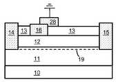
- FIG. 4shows a schematic illustration of a III-Nitride device, i.e., a III-Nitride HEMT, that includes a gate-connected field plate 28 , wherein the field plate is electrically connected to ground.
- This deviceis herein referred to as having a “grounded gate-connected field plate”.
- III-Nitride or III-N materials, layers, devices, etc.refer to a material or device comprised of a compound semiconductor material according to the stoichiometric formula Al x In y Ga z N, where x+y+z is about 1.
- two or more contacts or other itemsare said to be “electrically connected” if they are connected by a material which is sufficiently conducting to ensure that the electric potential at each of the contacts or other items is about the same at all times.
- a “ground terminal” or “ground”is a terminal with a potential (voltage) which the driver voltage signal is referenced relative to.
- the field platecan be connected to ground in a number of ways. For example, the field plate can be connected to ground directly by attaching one end of a conductive line to the field plate and the other end to ground. Or, the field plate can be directly mounted to a grounded portion of the circuit package, as illustrated in FIG. 8 and described below.
- the field platecan be connected to a terminal of the circuit package which remains grounded during circuit operation, as illustrated in FIG. 11 a and described below.
- Other grounding schemesare possible as well.
- the III-N HEMT shown in FIG. 4also comprises two III-N layers, a channel layer 11 such as GaN and a barrier layer 12 such as Al x Ga 1-x N.
- a 2DEG channel 19is in the channel layer 11 between the source and drain electrodes 14 and 15 adjacent to the interface between channel layer 11 and barrier layer 12 .
- the devicecan include any combination of III-N layers that results in a III-N HEMT structure.
- the devicecan include an additional III-N layer 20 such as a layer of AlN between channel layer 11 and barrier layer 12 , as shown in FIG. 5 .
- the devicecan comprise a series of III-N layers that results in two or more parallel 2DEG channels between the source and drain electrodes 14 and 15 .
- An example of a device with two 2DEG channelsis shown in FIG. 6 .
- This deviceincludes III-N layers 21 and 22 , which may be GaN and Al y Ga 1-y N, respectively, in addition to the layers shown in the device in FIG. 4 .
- the device in FIG. 6includes a 2DEG channel 19 in channel layer 11 and another in III-N layer 21 .
- the device in FIG. 6can be designed such that there is a 2DEG channel in layer 21 but no 2DEG channel in channel layer 11 , such as by including compensating dopants or other impurities, such as Fe or C, in channel layer 11 .
- the device in FIG. 6can be designed such that the 2DEG in channel layer 11 is substantially less conductive than, and in some cases eliminated with respect to, that in III-N layer 21 , such as by including compensating dopants or other impurities, such as Fe or C, in channel layer 11 .
- the field plateis comprised of a conducting material and in addition to being grounded, can be in any configuration that reduces the peak electric field in the device and thereby allows the device to operate at higher voltages.
- the field platecan include a single gate-connected field plate, as shown in FIG. 4 .
- the field platecan include multiple field plates, which is also referred to as a field plate with multiple portions, as shown in FIG. 7 .
- FIG. 7illustrates such a device, i.e., with two field plates 28 and 28 ′.
- the two field plates 28 , 28 ′are distinguished from one another by their distance from the barrier layer 12 , by whether they lie in a recess in an insulating layer or over the insulating layer or by the distance of their exposed upper surface from the insulator layer or a III-N layer of the device.
- all of the field platesare electrically connected to each other, at least one of the field plates is electrically connected to the gate, and at least one field plate is electrically connected to ground.
- FIG. 7shows the case where only field plate 28 ′ is connected to ground.
- the voltage on the field plateremains constant.
- the input capacitanceis unaffected by the field plate, and the field plate does not contribute to the Miller effect in the device.
- the manufacturing of circuits which comprise these devicescan be simplified, because the field plate can be directly mounted to a grounded portion of the package.
- An example of this mounting schemeis shown schematically in FIG. 8 , where a slant field plate 28 ′′ is directly mounted to grounded portion 30 of the package.
- a recess in the insulator layer 13has one or more slanted walls.
- the gate 16is shown as the portion that extends from the sides of the recess in the insulator layer 13 where the insulator layer 13 contacts the layer of material of below it that is different from the material of the insulator layer 13 , as shown in FIG. 8 barrier layer 12 .
- the gate 16extends vertically to the grounded portion 30 and the slant field plate 28 ′′ extends from the sidewalls of the gate 16 to the sidewalls of the recess.
- the slant field plate 28 ′′includes the potion of metal on the side of the gate closest to the drain electrode 15 .
- the grounded portion 30can be an electrically conductive layer that has a lateral dimension or a plan view surface area that is equal to or greater than a lateral dimension or plan view surface area of the transistor.
- the III-N devices illustrated in FIGS. 4-8are depletion mode (D-mode) devices, such that the device is in the ON state when the source electrode is at the same voltage as the gate electrode, and the voltage at the gate electrode must be less than that at the source electrode in order for the device to be switched OFF.
- the III-N devices illustrated in FIGS. 4-8can include a recess in the gate region of at least the III-N layer furthest from the substrate, wherein the gate electrode resides within the recess (not shown).
- the III-N devices illustrated in FIGS. 4-8can include an insulating material, i.e., a gate insulator, between the gate electrode and the III-N materials (not shown).
- Circuits and devices which comprise at least one transistor for which the voltage at the gate electrode remains constantcan include transistors configured as shown in FIGS. 4-9 .
- FIG. 9is a circuit representation of devices of the embodiments shown in FIGS. 4-8 , wherein the field plate 28 is connected to the gate and to ground, as shown.
- the use of these transistors in circuits and devicescan simplify the packaging and manufacturing process while at the same time prevent the Miller effect from degrading the performance of the circuits and devices.
- Embodiments of the circuits and devices that include a grounded gate-connected field plateare shown in FIGS. 10-13 .
- blocking a voltagerefers to the ability of a transistor to prevent significant current, such as current that is greater than 0.001 times the operating current during regular conduction, from flowing through the transistor when a voltage is applied across the transistor. In other words, while a transistor is blocking a voltage that is applied across it, the total current passing through the transistor will not be greater than 0.001 times the operating current during regular conduction.
- the embodiment represented by the circuit diagram of FIG. 10comprises an assembly including a high-voltage D-mode III-N transistor 40 with a grounded gate-connected field plate and a low voltage enhancement-mode (i.e., normally off) transistor 42 , where the source of the III-N transistor 40 is electrically connected to the drain of the enhancement-mode (E-mode) transistor 42 , and the source of the E-mode transistor 42 is electrically connected to ground.
- the assembly in FIG. 10operates similarly to a single high voltage E-mode transistor.
- an input voltage signal applied to node 46can produce an output signal at node 44 that is the same as the output signal produced at the drain terminal of a high voltage E-mode transistor when an input voltage signal is applied to the gate of the E-mode transistor and the source of the E-mode transistor is connected to ground.
- E-mode transistor 42blocks a voltage which is about equal to
- V this about ⁇ 5 to ⁇ 10 V.
- HVdepends on the particular circuit application, but HV is typically much larger than
- HVcan be about 600V, about 1200V, or any other voltage suitable for high voltage applications.
- the voltage at node 45is therefore about equal to
- the III-N transistor 40is capable of blocking large voltages, such as at least 600V or at least 1200V or other suitable blocking voltage required by the circuit applications. Furthermore, the threshold voltage V th of III-N transistor 40 must be sufficiently less than ⁇ V F such that when the assembly is in the ON state, the gate-source voltage V GS40 of III-N transistor 40 is sufficiently greater than V th so that III-N transistor 40 conducts the current flowing from node 44 to node 47 with sufficiently low conduction loss for the circuit application in which it is used.
- V thcan be less than ⁇ 3V, ⁇ 5V, or ⁇ 7V, and when the gate-source voltage V GS40 of III-N transistor 40 is about ⁇ V F , III-N transistor 40 can be capable of conducting 10 A of current or more with less than 7 W conduction loss.
- E-mode transistor 42is at least capable of blocking a voltage larger than
- E-mode transistor 42is a silicon (Si) based transistor, such as a vertical Si field-effect transistor (FET). In other embodiments, E-mode transistor 42 is a III-N based transistor, such as those described in U.S. patent application Ser. No. 11/856,687, filed Sep.
- the assembly shown in FIG. 10can also operate similarly to a single high-voltage E-mode transistor if the source of E-mode transistor 42 and the field plate of III-N transistor 40 are electrically connected to one another, rather than electrically connected to ground (not shown).
- FIGS. 11 a and 11 bshow a plan view and a cross-sectional view, respectively, of one possible configuration for the assembly of FIG. 10 after packaging. Only the relevant components of the package are included in the figure.
- E-mode transistor 42is a vertical low voltage Si MOS device (FET) and III-N transistor 40 is a horizontal high-voltage D-mode device, wherein III-N transistor 40 includes a grounded, gate-connected field plate 28 which is connected directly to a grounded portion 30 of the package, hereby referred to as the package base 30 .
- E-mode transistor 42is a III-N device, such as those described in U.S. patent application Ser. No. 11/856,687, filed Sep. 17, 2007, U.S. patent application Ser.
- E-mode transistor 42includes source, gate, and drain electrodes 64 , 66 , and 60 , respectively.
- E-mode transistor 42is mounted on a carrier 61
- carrier 61is mounted on the package base 30 .
- mounting one structure on another structureincludes bonding the structures using epoxy or solder bonds.
- the carrier 61at least comprises an electrically conductive layer 91 , such as gold (Au), adjacent to drain electrode 60 , and an electrically insulating layer 92 , such as AlN, adjacent to the package base 30 . Insulating layer 92 electrically isolates E-mode transistor 42 from the package base 30 .
- the III-N transistor 40includes source and drain electrodes 14 and 15 , respectively, as well as a gate electrode (not shown) which is connected to field plate 28 .
- field plate 28 of the III-N transistor 40 and source electrode 64 of the E-mode transistor 42are connected, such as by wire bonds or via holes, to the package base 30 .
- the electrically conductive layer of the carrier 61is connected, such as by wire bonds or copper stripes, to the source electrode 14 of III-N transistor 40 , thereby ensuring that drain electrode 60 of E-mode transistor 42 is electrically connected to the source electrode 14 of III-N transistor 40 .
- Gate electrode 66 of the E-mode transistor 42is connected, such as by wire bonding, to gate lead 76 on the package.
- Drain electrode 15 of the III-N transistor 40is connected, such as by wire bonding, to drain lead 74 on the package.
- the package base 30is connected, such as by wire bonding or copper stripes, to source lead 77 of the package.
- Terminal 47 on the source lead 77 of the packagecan be connected to ground.
- the entire package base 30can be bonded to a grounded material rather than connecting it to the source lead 77 of the package.
- the assembly shown in FIGS. 11 a and 11 bcan also operate similarly to a single high-voltage E-mode transistor if terminal 47 is not connected to ground (not shown).
- E-mode transistor 42is replaced with a low-voltage E-mode transistor which comprises a gate electrode and a drain electrode on the same side and a source electrode on the opposite side of the III-N layers that form the 2DEG from the gate/drain
- the low-voltage E-mode transistorcan be mounted directly on the package base 30 without having an insulator between the low-voltage E-mode transistor and the package base 30 .
- Thiseliminates the need for carrier 61 .
- Thisalso directly connects the source electrode to the package base 30 , i.e., directly connects two conductive portions together.
- the assembly in FIG. 12is similar to that in FIG. 10 , but further includes a diode 70 , where the anode of diode 70 is electrically connected to the drain of III-N transistor 40 .
- This assemblycan be used in circuit applications such as power factor correction (PFC).
- the diode 70comprises III-N materials.
- the diode 70can be formed of the same III-N materials as III-N transistor 40 , and diode 70 and III-N transistor 40 can furthermore be fabricated on the same chip.
- a complete description of III-N diodes that can be fabricated with the same III-N materials as III-N transistorscan be found in U.S. application Ser. No. 12/332,284, filed Dec. 10, 2008, which is hereby incorporated by reference throughout.
- the embodiment shown in FIG. 13comprises an assembly including a high-voltage D-mode III-N transistor 40 with a grounded gate-connected field plate and a low voltage diode 71 .
- the source of the III-N transistoris electrically connected to the cathode of the diode, and the anode of the diode is electrically connected to ground.
- the assembly in FIG. 13operates similarly to a single high-voltage diode. When the voltage at node 84 V 84 is greater than 0, the diode remains OFF (i.e. reverse biased), and no current flows from node 84 to node 87 .
- V 84is greater than 0 but less than
- V 84is increased above
- V 84is forward biased in the ON state, current flows from node 87 to node 84 .
- the voltage at node 84must be less than about ⁇
- This assemblycan be preferable to a single high-voltage diode, because the turn-on voltage of a low-voltage diode is typically lower than that of a high-voltage diode, so the assembly in FIG. 13 can have lower forward conduction loss than a single high-voltage diode.
- the low-voltage diode 71is a Si-based diode. In other embodiments, the low-voltage diode 71 comprises III-N materials. In still other embodiments, the diode 71 comprises the same III-N materials as III-N transistor 40 , and diode 71 and III-N transistor 40 can furthermore be fabricated on the same chip.
- the III-N transistor 40is capable of blocking large voltages, such as at least 600V or at least 1200V or other suitable blocking voltage required by the circuit applications. Furthermore, when the assembly is forward biased such that current flows through the diode 71 and through the III-N transistor 40 , the voltage at node 85 is about ⁇
- the gate-source voltage V GS40 of III-N transistor 40 under these bias conditionsis about equal to
- the threshold voltage V th of III-N transistor 40must be sufficiently less than
- can be about 0.2 V or less
- V thcan be less than ⁇ 3V, ⁇ 5V, or ⁇ 7V
- the gate-source voltage V GS40 of III-N transistor 40is about equal to
- the assembly shown in FIG. 13can also operate similarly to a single high-voltage diode if the anode of low-voltage diode 71 and the field plate of III-N transistor 40 are electrically connected to one another, rather than electrically connected to ground (not shown).
- FIGS. 4-8Other features which are well known to be beneficial to device performance can also be included in the structures in FIGS. 4-8 . These include but are not limited to gate insulators between the gate electrode and III-N layers, surface passivation layers, and recesses in the gate region of the III-N materials. These features can be used individually or in combination with one another.
Landscapes
- Engineering & Computer Science (AREA)
- Power Engineering (AREA)
- Microelectronics & Electronic Packaging (AREA)
- Physics & Mathematics (AREA)
- Condensed Matter Physics & Semiconductors (AREA)
- General Physics & Mathematics (AREA)
- Computer Hardware Design (AREA)
- Junction Field-Effect Transistors (AREA)
- Semiconductor Integrated Circuits (AREA)
Abstract
Description
Claims (23)
Priority Applications (6)
| Application Number | Priority Date | Filing Date | Title |
|---|---|---|---|
| US12/368,248US7884394B2 (en) | 2009-02-09 | 2009-02-09 | III-nitride devices and circuits |
| CN2010800072368ACN102308387A (en) | 2009-02-09 | 2010-01-22 | III-nitride devices and circuits |
| JP2011549175AJP2012517699A (en) | 2009-02-09 | 2010-01-22 | III-nitride devices and circuits |
| EP10738957.9AEP2394303A4 (en) | 2009-02-09 | 2010-01-22 | GROUP III NITRIDE DEVICES AND CIRCUITS |
| PCT/US2010/021824WO2010090885A2 (en) | 2009-02-09 | 2010-01-22 | Iii-nitride devices and circuits |
| TW099103836ATWI475691B (en) | 2009-02-09 | 2010-02-08 | Group III nitride devices and circuits |
Applications Claiming Priority (1)
| Application Number | Priority Date | Filing Date | Title |
|---|---|---|---|
| US12/368,248US7884394B2 (en) | 2009-02-09 | 2009-02-09 | III-nitride devices and circuits |
Publications (2)
| Publication Number | Publication Date |
|---|---|
| US20100201439A1 US20100201439A1 (en) | 2010-08-12 |
| US7884394B2true US7884394B2 (en) | 2011-02-08 |
Family
ID=42539936
Family Applications (1)
| Application Number | Title | Priority Date | Filing Date |
|---|---|---|---|
| US12/368,248Active2029-08-15US7884394B2 (en) | 2009-02-09 | 2009-02-09 | III-nitride devices and circuits |
Country Status (6)
| Country | Link |
|---|---|
| US (1) | US7884394B2 (en) |
| EP (1) | EP2394303A4 (en) |
| JP (1) | JP2012517699A (en) |
| CN (1) | CN102308387A (en) |
| TW (1) | TWI475691B (en) |
| WO (1) | WO2010090885A2 (en) |
Cited By (39)
| Publication number | Priority date | Publication date | Assignee | Title |
|---|---|---|---|---|
| US20090072269A1 (en)* | 2007-09-17 | 2009-03-19 | Chang Soo Suh | Gallium nitride diodes and integrated components |
| US20100289067A1 (en)* | 2009-05-14 | 2010-11-18 | Transphorm Inc. | High Voltage III-Nitride Semiconductor Devices |
| US20110049526A1 (en)* | 2009-08-28 | 2011-03-03 | Transphorm Inc. | Semiconductor Devices with Field Plates |
| US20110215378A1 (en)* | 2010-03-02 | 2011-09-08 | Samsung Electronics Co., Ltd. | High electron mobility transistors exhibiting dual depletion and methods of manufacturing the same |
| US8289065B2 (en) | 2008-09-23 | 2012-10-16 | Transphorm Inc. | Inductive load power switching circuits |
| US8344424B2 (en) | 2007-09-17 | 2013-01-01 | Transphorm Inc. | Enhancement mode gallium nitride power devices |
| US8455931B2 (en) | 2009-11-02 | 2013-06-04 | Transphorm Inc. | Package configurations for low EMI circuits |
| US8519438B2 (en) | 2008-04-23 | 2013-08-27 | Transphorm Inc. | Enhancement mode III-N HEMTs |
| US8598937B2 (en) | 2011-10-07 | 2013-12-03 | Transphorm Inc. | High power semiconductor electronic components with increased reliability |
| US8710511B2 (en) | 2011-07-29 | 2014-04-29 | Northrop Grumman Systems Corporation | AIN buffer N-polar GaN HEMT profile |
| US8716141B2 (en) | 2011-03-04 | 2014-05-06 | Transphorm Inc. | Electrode configurations for semiconductor devices |
| US8772842B2 (en) | 2011-03-04 | 2014-07-08 | Transphorm, Inc. | Semiconductor diodes with low reverse bias currents |
| US8786327B2 (en) | 2011-02-28 | 2014-07-22 | Transphorm Inc. | Electronic components with reactive filters |
| US8816497B2 (en) | 2010-01-08 | 2014-08-26 | Transphorm Inc. | Electronic devices and components for high efficiency power circuits |
| US20140266324A1 (en)* | 2013-03-15 | 2014-09-18 | Mitsubishi Electric Research Laboratories, Inc. | High Electron Mobility Transistor with Multiple Channels |
| US20150041984A1 (en)* | 2013-08-09 | 2015-02-12 | Infineon Technologies Austria Ag | Electronic Component and Method |
| US9059076B2 (en) | 2013-04-01 | 2015-06-16 | Transphorm Inc. | Gate drivers for circuits based on semiconductor devices |
| US9087718B2 (en) | 2013-03-13 | 2015-07-21 | Transphorm Inc. | Enhancement-mode III-nitride devices |
| US9093366B2 (en) | 2012-04-09 | 2015-07-28 | Transphorm Inc. | N-polar III-nitride transistors |
| US9166006B1 (en)* | 2013-12-08 | 2015-10-20 | Iman Rezanezhad Gatabi | Methods to improve the performance of compound semiconductor devices and field effect transistors |
| US20150340483A1 (en)* | 2014-05-21 | 2015-11-26 | International Rectifier Corporation | Group III-V Device Including a Shield Plate |
| US9245993B2 (en) | 2013-03-15 | 2016-01-26 | Transphorm Inc. | Carbon doping semiconductor devices |
| US9318593B2 (en) | 2014-07-21 | 2016-04-19 | Transphorm Inc. | Forming enhancement mode III-nitride devices |
| US9443938B2 (en) | 2013-07-19 | 2016-09-13 | Transphorm Inc. | III-nitride transistor including a p-type depleting layer |
| US9496137B2 (en) | 2009-12-10 | 2016-11-15 | Transphorm Inc. | Methods of forming reverse side engineered III-nitride devices |
| US9536967B2 (en) | 2014-12-16 | 2017-01-03 | Transphorm Inc. | Recessed ohmic contacts in a III-N device |
| US9536966B2 (en) | 2014-12-16 | 2017-01-03 | Transphorm Inc. | Gate structures for III-N devices |
| US9537425B2 (en) | 2013-07-09 | 2017-01-03 | Transphorm Inc. | Multilevel inverters and their components |
| US9543940B2 (en) | 2014-07-03 | 2017-01-10 | Transphorm Inc. | Switching circuits having ferrite beads |
| US9590494B1 (en) | 2014-07-17 | 2017-03-07 | Transphorm Inc. | Bridgeless power factor correction circuits |
| US9899998B2 (en) | 2008-02-12 | 2018-02-20 | Transphorm Inc. | Bridge circuits and their components |
| US10224401B2 (en) | 2016-05-31 | 2019-03-05 | Transphorm Inc. | III-nitride devices including a graded depleting layer |
| US20190214493A1 (en)* | 2011-12-21 | 2019-07-11 | Power Integrations, Inc. | Shield wrap for a heterostructure field effect transistor |
| US10630285B1 (en) | 2017-11-21 | 2020-04-21 | Transphorm Technology, Inc. | Switching circuits having drain connected ferrite beads |
| US10756207B2 (en) | 2018-10-12 | 2020-08-25 | Transphorm Technology, Inc. | Lateral III-nitride devices including a vertical gate module |
| US11322599B2 (en) | 2016-01-15 | 2022-05-03 | Transphorm Technology, Inc. | Enhancement mode III-nitride devices having an Al1-xSixO gate insulator |
| US11749656B2 (en) | 2020-06-16 | 2023-09-05 | Transphorm Technology, Inc. | Module configurations for integrated III-Nitride devices |
| US11810971B2 (en) | 2019-03-21 | 2023-11-07 | Transphorm Technology, Inc. | Integrated design for III-Nitride devices |
| US11973138B2 (en) | 2020-08-05 | 2024-04-30 | Transphorm Technology, Inc. | N-polar devices including a depleting layer with improved conductivity |
Families Citing this family (46)
| Publication number | Priority date | Publication date | Assignee | Title |
|---|---|---|---|---|
| US7501669B2 (en) | 2003-09-09 | 2009-03-10 | Cree, Inc. | Wide bandgap transistor devices with field plates |
| US9773877B2 (en) | 2004-05-13 | 2017-09-26 | Cree, Inc. | Wide bandgap field effect transistors with source connected field plates |
| US11791385B2 (en) | 2005-03-11 | 2023-10-17 | Wolfspeed, Inc. | Wide bandgap transistors with gate-source field plates |
| US7898004B2 (en) | 2008-12-10 | 2011-03-01 | Transphorm Inc. | Semiconductor heterostructure diodes |
| US8624662B2 (en) | 2010-02-05 | 2014-01-07 | Transphorm Inc. | Semiconductor electronic components and circuits |
| US8742460B2 (en)* | 2010-12-15 | 2014-06-03 | Transphorm Inc. | Transistors with isolation regions |
| US8643062B2 (en) | 2011-02-02 | 2014-02-04 | Transphorm Inc. | III-N device structures and methods |
| JP5776217B2 (en)* | 2011-02-24 | 2015-09-09 | 富士通株式会社 | Compound semiconductor device |
| WO2013005372A1 (en)* | 2011-07-01 | 2013-01-10 | パナソニック株式会社 | Semiconductor device |
| US8674372B2 (en)* | 2011-08-19 | 2014-03-18 | Infineon Technologies Austria Ag | HEMT with integrated low forward bias diode |
| US8901604B2 (en) | 2011-09-06 | 2014-12-02 | Transphorm Inc. | Semiconductor devices with guard rings |
| US9257547B2 (en) | 2011-09-13 | 2016-02-09 | Transphorm Inc. | III-N device structures having a non-insulating substrate |
| US9209176B2 (en)* | 2011-12-07 | 2015-12-08 | Transphorm Inc. | Semiconductor modules and methods of forming the same |
| US20130146943A1 (en)* | 2011-12-12 | 2013-06-13 | John P. EDWARDS | In situ grown gate dielectric and field plate dielectric |
| US9165766B2 (en) | 2012-02-03 | 2015-10-20 | Transphorm Inc. | Buffer layer structures suited for III-nitride devices with foreign substrates |
| US8648643B2 (en) | 2012-02-24 | 2014-02-11 | Transphorm Inc. | Semiconductor power modules and devices |
| US9184275B2 (en) | 2012-06-27 | 2015-11-10 | Transphorm Inc. | Semiconductor devices with integrated hole collectors |
| US8803246B2 (en) | 2012-07-16 | 2014-08-12 | Transphorm Inc. | Semiconductor electronic components with integrated current limiters |
| US20140021934A1 (en)* | 2012-07-17 | 2014-01-23 | Transphorm, Inc. | Devices and components for power conversion circuits |
| CN103824845B (en)* | 2012-11-19 | 2017-08-29 | 台达电子工业股份有限公司 | Semiconductor device with a plurality of semiconductor chips |
| US9799762B2 (en) | 2012-12-03 | 2017-10-24 | Infineon Technologies Ag | Semiconductor device and method of manufacturing a semiconductor device |
| US9171837B2 (en) | 2012-12-17 | 2015-10-27 | Nxp B.V. | Cascode circuit |
| CN105164811B (en) | 2013-02-15 | 2018-08-31 | 创世舫电子有限公司 | Electrode of semiconductor devices and forming method thereof |
| JP2014187086A (en)* | 2013-03-22 | 2014-10-02 | Toshiba Corp | Semiconductor device |
| US9755059B2 (en) | 2013-06-09 | 2017-09-05 | Cree, Inc. | Cascode structures with GaN cap layers |
| US9847411B2 (en)* | 2013-06-09 | 2017-12-19 | Cree, Inc. | Recessed field plate transistor structures |
| US9679981B2 (en) | 2013-06-09 | 2017-06-13 | Cree, Inc. | Cascode structures for GaN HEMTs |
| US9287404B2 (en) | 2013-10-02 | 2016-03-15 | Infineon Technologies Austria Ag | Semiconductor device and method of manufacturing a semiconductor device with lateral FET cells and field plates |
| US9306058B2 (en)* | 2013-10-02 | 2016-04-05 | Infineon Technologies Ag | Integrated circuit and method of manufacturing an integrated circuit |
| US9401399B2 (en) | 2013-10-15 | 2016-07-26 | Infineon Technologies Ag | Semiconductor device |
| US9048838B2 (en)* | 2013-10-30 | 2015-06-02 | Infineon Technologies Austria Ag | Switching circuit |
| CN104332498B (en)* | 2014-09-01 | 2018-01-05 | 苏州捷芯威半导体有限公司 | A kind of tiltedly preparation method of field plate power device and oblique field plate power device |
| CN104241400B (en)* | 2014-09-05 | 2017-03-08 | 苏州捷芯威半导体有限公司 | Field-effect diode and preparation method thereof |
| US10290566B2 (en)* | 2014-09-23 | 2019-05-14 | Infineon Technologies Austria Ag | Electronic component |
| WO2016149146A1 (en) | 2015-03-13 | 2016-09-22 | Transphorm, Inc. | Paralleling of switching devices for high power circuits |
| DE102015117394B4 (en)* | 2015-10-13 | 2020-06-18 | Infineon Technologies Austria Ag | Semiconductor device |
| US9929261B2 (en) | 2016-04-07 | 2018-03-27 | Semiconductor Components Industries, Llc | Electronic device including a HEMT with a segmented gate electrode |
| US10319648B2 (en) | 2017-04-17 | 2019-06-11 | Transphorm Inc. | Conditions for burn-in of high power semiconductors |
| CN107507858B (en)* | 2017-08-28 | 2021-04-20 | 电子科技大学 | A current limiting diode |
| CN111183523A (en)* | 2018-01-12 | 2020-05-19 | 英特尔公司 | Transistor including first and second semiconductor materials between source and drain regions and method of making the same |
| CN110620143A (en)* | 2018-06-20 | 2019-12-27 | 夏令 | Mixed channel compound semiconductor device |
| US11239802B2 (en)* | 2019-10-02 | 2022-02-01 | Wolfspeed, Inc. | Radio frequency transistor amplifiers having engineered instrinsic capacitances for improved performance |
| CN110828565B (en)* | 2019-10-30 | 2022-03-15 | 杭州电子科技大学 | A dual-channel high-voltage gallium nitride field effect transistor with a P-type buried layer |
| US11387095B2 (en)* | 2020-08-21 | 2022-07-12 | Infineon Technologies Austria Ag | Passivation structuring and plating for semiconductor devices |
| CN112821740B (en)* | 2021-01-22 | 2025-09-12 | 常州佳讯光电产业发展有限公司 | A silicon carbide MOSFET internal driver protection device |
| CN117747654A (en)* | 2022-09-14 | 2024-03-22 | 乂馆信息科技(上海)有限公司 | A new topology HEMT device |
Citations (5)
| Publication number | Priority date | Publication date | Assignee | Title |
|---|---|---|---|---|
| US20060102929A1 (en) | 2002-12-16 | 2006-05-18 | Yasuhiro Okamoto | Field-effect transistor |
| US20070018210A1 (en) | 2005-07-21 | 2007-01-25 | Cree, Inc. | Switch mode power amplifier using MIS-HEMT with field plate extension |
| US7304331B2 (en) | 2004-07-14 | 2007-12-04 | Kabushiki Kaisha Toshiba | Nitride semiconductor device such as transverse power FET for high frequency signal amplification or power control |
| US20080283844A1 (en) | 2007-05-16 | 2008-11-20 | Oki Electric Industry Co., Ltd. | Method for manufacturing a field effect transistor having a field plate |
| US7501669B2 (en)* | 2003-09-09 | 2009-03-10 | Cree, Inc. | Wide bandgap transistor devices with field plates |
Family Cites Families (15)
| Publication number | Priority date | Publication date | Assignee | Title |
|---|---|---|---|---|
| US6028348A (en)* | 1993-11-30 | 2000-02-22 | Texas Instruments Incorporated | Low thermal impedance integrated circuit |
| WO2004068590A1 (en)* | 2003-01-29 | 2004-08-12 | Kabushiki Kaisha Toshiba | Power semiconductor device |
| TWI404208B (en)* | 2003-09-09 | 2013-08-01 | Cree Inc | Wide band gap transistor device with field plate |
| JP2005159117A (en)* | 2003-11-27 | 2005-06-16 | Toshiba Corp | Nitride semiconductor devices |
| WO2005081304A1 (en)* | 2004-02-20 | 2005-09-01 | Nec Corporation | Field effect transistor |
| US7550783B2 (en)* | 2004-05-11 | 2009-06-23 | Cree, Inc. | Wide bandgap HEMTs with source connected field plates |
| TW200627627A (en)* | 2004-09-24 | 2006-08-01 | Koninkl Philips Electronics Nv | Enhancement-depletion field effect transistor structure and method of manufacture |
| JP2007250792A (en)* | 2006-03-15 | 2007-09-27 | Furukawa Electric Co Ltd:The | Semiconductor element |
| JP2009530862A (en)* | 2006-03-20 | 2009-08-27 | インターナショナル レクティファイアー コーポレイション | Merged gate cascode transistor |
| TW200746414A (en)* | 2006-06-05 | 2007-12-16 | Win Semiconductors Corp | A structure and a method for monolithic integration of HBT, depletion-mode HEMT and enhancement-mode HEMT on the same substrate |
| TW200830550A (en)* | 2006-08-18 | 2008-07-16 | Univ California | High breakdown enhancement mode gallium nitride based high electron mobility transistors with integrated slant field plate |
| EP2080228B1 (en)* | 2006-10-04 | 2020-12-02 | LEONARDO S.p.A. | Single voltage supply pseudomorphic high electron mobility transistor (phemt) power device and process for manufacturing the same |
| JP5358882B2 (en)* | 2007-02-09 | 2013-12-04 | サンケン電気株式会社 | Composite semiconductor device including rectifying element |
| US7501670B2 (en)* | 2007-03-20 | 2009-03-10 | Velox Semiconductor Corporation | Cascode circuit employing a depletion-mode, GaN-based FET |
| US8502323B2 (en) | 2007-08-03 | 2013-08-06 | The Hong Kong University Of Science And Technology | Reliable normally-off III-nitride active device structures, and related methods and systems |
- 2009
- 2009-02-09USUS12/368,248patent/US7884394B2/enactiveActive
- 2010
- 2010-01-22CNCN2010800072368Apatent/CN102308387A/enactivePending
- 2010-01-22WOPCT/US2010/021824patent/WO2010090885A2/enactiveApplication Filing
- 2010-01-22JPJP2011549175Apatent/JP2012517699A/enactivePending
- 2010-01-22EPEP10738957.9Apatent/EP2394303A4/ennot_activeWithdrawn
- 2010-02-08TWTW099103836Apatent/TWI475691B/enactive
Patent Citations (5)
| Publication number | Priority date | Publication date | Assignee | Title |
|---|---|---|---|---|
| US20060102929A1 (en) | 2002-12-16 | 2006-05-18 | Yasuhiro Okamoto | Field-effect transistor |
| US7501669B2 (en)* | 2003-09-09 | 2009-03-10 | Cree, Inc. | Wide bandgap transistor devices with field plates |
| US7304331B2 (en) | 2004-07-14 | 2007-12-04 | Kabushiki Kaisha Toshiba | Nitride semiconductor device such as transverse power FET for high frequency signal amplification or power control |
| US20070018210A1 (en) | 2005-07-21 | 2007-01-25 | Cree, Inc. | Switch mode power amplifier using MIS-HEMT with field plate extension |
| US20080283844A1 (en) | 2007-05-16 | 2008-11-20 | Oki Electric Industry Co., Ltd. | Method for manufacturing a field effect transistor having a field plate |
Non-Patent Citations (6)
| Title |
|---|
| Chung, Sung Chan, authorized officer, International Search Report and Written Opinion for PCT/US2010/021824 mailed Aug.23, 2010, 9 pages. |
| Mishra et al., "Enhancement Mode III-N. HEMTs", U.S. Appl. No. 12/108,449, filed Apr. 23, 2008, 58 pp. |
| Suh et al., "Enhancement Mode Nitride Power Devices", U.S. Appl. No. 11/856,687, filed Sep. 17, 2007, 58 pp. |
| Suh et al., "III-Nitride Devices with Recessed Gates", U.S. Appl. No. 12/102,340, filed Apr. 14, 2008, 29 pp. |
| Suh et al., "Insulated Gate E-Mode Transistors", U.S. Appl. No. 12/324,574, filed Nov. 26, 2008, 43 pp. |
| Wu et al., "Semiconductor Heterostructure Diodes", U.S. Appl. No. 12/332,284, filed Dec. 10, 2008, 51 pp. |
Cited By (67)
| Publication number | Priority date | Publication date | Assignee | Title |
|---|---|---|---|---|
| US20090072269A1 (en)* | 2007-09-17 | 2009-03-19 | Chang Soo Suh | Gallium nitride diodes and integrated components |
| US9343560B2 (en) | 2007-09-17 | 2016-05-17 | Transphorm Inc. | Gallium nitride power devices |
| US8344424B2 (en) | 2007-09-17 | 2013-01-01 | Transphorm Inc. | Enhancement mode gallium nitride power devices |
| US8633518B2 (en) | 2007-09-17 | 2014-01-21 | Transphorm Inc. | Gallium nitride power devices |
| US9899998B2 (en) | 2008-02-12 | 2018-02-20 | Transphorm Inc. | Bridge circuits and their components |
| US8519438B2 (en) | 2008-04-23 | 2013-08-27 | Transphorm Inc. | Enhancement mode III-N HEMTs |
| US8289065B2 (en) | 2008-09-23 | 2012-10-16 | Transphorm Inc. | Inductive load power switching circuits |
| US8531232B2 (en) | 2008-09-23 | 2013-09-10 | Transphorm Inc. | Inductive load power switching circuits |
| US20100289067A1 (en)* | 2009-05-14 | 2010-11-18 | Transphorm Inc. | High Voltage III-Nitride Semiconductor Devices |
| US9293561B2 (en) | 2009-05-14 | 2016-03-22 | Transphorm Inc. | High voltage III-nitride semiconductor devices |
| US8390000B2 (en) | 2009-08-28 | 2013-03-05 | Transphorm Inc. | Semiconductor devices with field plates |
| US9831315B2 (en) | 2009-08-28 | 2017-11-28 | Transphorm Inc. | Semiconductor devices with field plates |
| US9111961B2 (en) | 2009-08-28 | 2015-08-18 | Transphorm Inc. | Semiconductor devices with field plates |
| US9373699B2 (en) | 2009-08-28 | 2016-06-21 | Transphorm Inc. | Semiconductor devices with field plates |
| US20110049526A1 (en)* | 2009-08-28 | 2011-03-03 | Transphorm Inc. | Semiconductor Devices with Field Plates |
| US8455931B2 (en) | 2009-11-02 | 2013-06-04 | Transphorm Inc. | Package configurations for low EMI circuits |
| US9190295B2 (en) | 2009-11-02 | 2015-11-17 | Transphorm Inc. | Package configurations for low EMI circuits |
| US9496137B2 (en) | 2009-12-10 | 2016-11-15 | Transphorm Inc. | Methods of forming reverse side engineered III-nitride devices |
| US8816497B2 (en) | 2010-01-08 | 2014-08-26 | Transphorm Inc. | Electronic devices and components for high efficiency power circuits |
| US9401341B2 (en) | 2010-01-08 | 2016-07-26 | Transphorm Inc. | Electronic devices and components for high efficiency power circuits |
| US9660048B2 (en)* | 2010-03-02 | 2017-05-23 | Samsung Electronics Co., Ltd. | High electron mobility transistors exhibiting dual depletion and methods of manufacturing the same |
| US20110215378A1 (en)* | 2010-03-02 | 2011-09-08 | Samsung Electronics Co., Ltd. | High electron mobility transistors exhibiting dual depletion and methods of manufacturing the same |
| US8786327B2 (en) | 2011-02-28 | 2014-07-22 | Transphorm Inc. | Electronic components with reactive filters |
| US8716141B2 (en) | 2011-03-04 | 2014-05-06 | Transphorm Inc. | Electrode configurations for semiconductor devices |
| US8772842B2 (en) | 2011-03-04 | 2014-07-08 | Transphorm, Inc. | Semiconductor diodes with low reverse bias currents |
| US8710511B2 (en) | 2011-07-29 | 2014-04-29 | Northrop Grumman Systems Corporation | AIN buffer N-polar GaN HEMT profile |
| US9171836B2 (en) | 2011-10-07 | 2015-10-27 | Transphorm Inc. | Method of forming electronic components with increased reliability |
| US8598937B2 (en) | 2011-10-07 | 2013-12-03 | Transphorm Inc. | High power semiconductor electronic components with increased reliability |
| US20190214493A1 (en)* | 2011-12-21 | 2019-07-11 | Power Integrations, Inc. | Shield wrap for a heterostructure field effect transistor |
| US9093366B2 (en) | 2012-04-09 | 2015-07-28 | Transphorm Inc. | N-polar III-nitride transistors |
| US9490324B2 (en) | 2012-04-09 | 2016-11-08 | Transphorm Inc. | N-polar III-nitride transistors |
| US9087718B2 (en) | 2013-03-13 | 2015-07-21 | Transphorm Inc. | Enhancement-mode III-nitride devices |
| US20140266324A1 (en)* | 2013-03-15 | 2014-09-18 | Mitsubishi Electric Research Laboratories, Inc. | High Electron Mobility Transistor with Multiple Channels |
| US9245993B2 (en) | 2013-03-15 | 2016-01-26 | Transphorm Inc. | Carbon doping semiconductor devices |
| US9245992B2 (en) | 2013-03-15 | 2016-01-26 | Transphorm Inc. | Carbon doping semiconductor devices |
| US9865719B2 (en) | 2013-03-15 | 2018-01-09 | Transphorm Inc. | Carbon doping semiconductor devices |
| US8907378B2 (en)* | 2013-03-15 | 2014-12-09 | Mitsubishi Electric Research Laboratories, Inc. | High electron mobility transistor with multiple channels |
| US9059076B2 (en) | 2013-04-01 | 2015-06-16 | Transphorm Inc. | Gate drivers for circuits based on semiconductor devices |
| US9537425B2 (en) | 2013-07-09 | 2017-01-03 | Transphorm Inc. | Multilevel inverters and their components |
| US10043896B2 (en) | 2013-07-19 | 2018-08-07 | Transphorm Inc. | III-Nitride transistor including a III-N depleting layer |
| US9443938B2 (en) | 2013-07-19 | 2016-09-13 | Transphorm Inc. | III-nitride transistor including a p-type depleting layer |
| US9842922B2 (en) | 2013-07-19 | 2017-12-12 | Transphorm Inc. | III-nitride transistor including a p-type depleting layer |
| US9443787B2 (en)* | 2013-08-09 | 2016-09-13 | Infineon Technologies Austria Ag | Electronic component and method |
| US9620472B2 (en) | 2013-08-09 | 2017-04-11 | Infineon Technologies Austria Ag | Method of manufacturing an electronic component |
| US20150041984A1 (en)* | 2013-08-09 | 2015-02-12 | Infineon Technologies Austria Ag | Electronic Component and Method |
| US9166006B1 (en)* | 2013-12-08 | 2015-10-20 | Iman Rezanezhad Gatabi | Methods to improve the performance of compound semiconductor devices and field effect transistors |
| US20150340483A1 (en)* | 2014-05-21 | 2015-11-26 | International Rectifier Corporation | Group III-V Device Including a Shield Plate |
| US9543940B2 (en) | 2014-07-03 | 2017-01-10 | Transphorm Inc. | Switching circuits having ferrite beads |
| US9590494B1 (en) | 2014-07-17 | 2017-03-07 | Transphorm Inc. | Bridgeless power factor correction circuits |
| US9935190B2 (en) | 2014-07-21 | 2018-04-03 | Transphorm Inc. | Forming enhancement mode III-nitride devices |
| US9318593B2 (en) | 2014-07-21 | 2016-04-19 | Transphorm Inc. | Forming enhancement mode III-nitride devices |
| US9536966B2 (en) | 2014-12-16 | 2017-01-03 | Transphorm Inc. | Gate structures for III-N devices |
| US9536967B2 (en) | 2014-12-16 | 2017-01-03 | Transphorm Inc. | Recessed ohmic contacts in a III-N device |
| US11322599B2 (en) | 2016-01-15 | 2022-05-03 | Transphorm Technology, Inc. | Enhancement mode III-nitride devices having an Al1-xSixO gate insulator |
| US10224401B2 (en) | 2016-05-31 | 2019-03-05 | Transphorm Inc. | III-nitride devices including a graded depleting layer |
| US10629681B2 (en) | 2016-05-31 | 2020-04-21 | Transphorm Technology, Inc. | III-nitride devices including a graded depleting layer |
| US11121216B2 (en) | 2016-05-31 | 2021-09-14 | Transphorm Technology, Inc. | III-nitride devices including a graded depleting layer |
| US10897249B1 (en) | 2017-11-21 | 2021-01-19 | Transphorm Technology, Inc. | Switching circuits having drain connected ferrite beads |
| US11309884B1 (en) | 2017-11-21 | 2022-04-19 | Transphorm Technology, Inc. | Switching circuits having drain connected ferrite beads |
| US10630285B1 (en) | 2017-11-21 | 2020-04-21 | Transphorm Technology, Inc. | Switching circuits having drain connected ferrite beads |
| US10756207B2 (en) | 2018-10-12 | 2020-08-25 | Transphorm Technology, Inc. | Lateral III-nitride devices including a vertical gate module |
| US12266725B2 (en) | 2018-10-12 | 2025-04-01 | Transphorm Technology, Inc. | Lateral III-nitride devices including a vertical gate module |
| US11810971B2 (en) | 2019-03-21 | 2023-11-07 | Transphorm Technology, Inc. | Integrated design for III-Nitride devices |
| US12324180B2 (en) | 2019-03-21 | 2025-06-03 | Transphorm Technology, Inc. | Integrated design for III-Nitride devices |
| US11749656B2 (en) | 2020-06-16 | 2023-09-05 | Transphorm Technology, Inc. | Module configurations for integrated III-Nitride devices |
| US12074150B2 (en) | 2020-06-16 | 2024-08-27 | Transphorm Technology, Inc. | Module configurations for integrated III-nitride devices |
| US11973138B2 (en) | 2020-08-05 | 2024-04-30 | Transphorm Technology, Inc. | N-polar devices including a depleting layer with improved conductivity |
Also Published As
| Publication number | Publication date |
|---|---|
| WO2010090885A3 (en) | 2010-10-21 |
| TW201036155A (en) | 2010-10-01 |
| US20100201439A1 (en) | 2010-08-12 |
| CN102308387A (en) | 2012-01-04 |
| EP2394303A2 (en) | 2011-12-14 |
| TWI475691B (en) | 2015-03-01 |
| JP2012517699A (en) | 2012-08-02 |
| EP2394303A4 (en) | 2013-04-17 |
| WO2010090885A2 (en) | 2010-08-12 |
Similar Documents
| Publication | Publication Date | Title |
|---|---|---|
| US7884394B2 (en) | III-nitride devices and circuits | |
| US10607978B2 (en) | Semiconductor device and electronic apparatus | |
| US12324180B2 (en) | Integrated design for III-Nitride devices | |
| US20210391311A1 (en) | Module configurations for integrated iii-nitride devices | |
| US10290566B2 (en) | Electronic component | |
| KR101539531B1 (en) | Semiconductor device | |
| US9190295B2 (en) | Package configurations for low EMI circuits | |
| US9654001B2 (en) | Semiconductor device | |
| JP5883799B2 (en) | Electronic devices and components for high efficiency power circuits | |
| US8987833B2 (en) | Stacked composite device including a group III-V transistor and a group IV lateral transistor | |
| US11631741B2 (en) | Semiconductor device | |
| US20180097070A1 (en) | Semiconductor device | |
| US12284825B2 (en) | Semiconductor device including electrodes with identical potential | |
| US20120256190A1 (en) | Stacked Composite Device Including a Group III-V Transistor and a Group IV Diode | |
| WO2024167620A1 (en) | Configurations for four quadrant iii-nitride switches |
Legal Events
| Date | Code | Title | Description |
|---|---|---|---|
| AS | Assignment | Owner name:TRANSPHORM INC., CALIFORNIA Free format text:ASSIGNMENT OF ASSIGNORS INTEREST;ASSIGNORS:WU, YIFENG;CHU, RONGMING;REEL/FRAME:022523/0790 Effective date:20090206 | |
| STCF | Information on status: patent grant | Free format text:PATENTED CASE | |
| FPAY | Fee payment | Year of fee payment:4 | |
| AS | Assignment | Owner name:NEXPERIA B.V., NETHERLANDS Free format text:SECURITY INTEREST;ASSIGNOR:TRANSPHORM, INC.;REEL/FRAME:045853/0159 Effective date:20180404 | |
| MAFP | Maintenance fee payment | Free format text:PAYMENT OF MAINTENANCE FEE, 8TH YR, SMALL ENTITY (ORIGINAL EVENT CODE: M2552) Year of fee payment:8 | |
| AS | Assignment | Owner name:TRANSPHORM TECHNOLOGY, INC., CALIFORNIA Free format text:CHANGE OF NAME;ASSIGNOR:TRANSPHORM, INC.;REEL/FRAME:052091/0697 Effective date:20200212 | |
| MAFP | Maintenance fee payment | Free format text:PAYMENT OF MAINTENANCE FEE, 12TH YR, SMALL ENTITY (ORIGINAL EVENT CODE: M2553); ENTITY STATUS OF PATENT OWNER: SMALL ENTITY Year of fee payment:12 | |
| AS | Assignment | Owner name:RENESAS ELECTRONICS AMERICA INC., JAPAN Free format text:SECURITY INTEREST;ASSIGNORS:TRANSPHORM TECHNOLOGY, INC.;TRANSPHORM, INC.;REEL/FRAME:066713/0531 Effective date:20240301 |