US7882406B2 - Built in test controller with a downloadable testing program - Google Patents
Built in test controller with a downloadable testing programDownload PDFInfo
- Publication number
- US7882406B2 US7882406B2US12/118,477US11847708AUS7882406B2US 7882406 B2US7882406 B2US 7882406B2US 11847708 AUS11847708 AUS 11847708AUS 7882406 B2US7882406 B2US 7882406B2
- Authority
- US
- United States
- Prior art keywords
- signal
- response
- control signal
- read address
- testing
- Prior art date
- Legal status (The legal status is an assumption and is not a legal conclusion. Google has not performed a legal analysis and makes no representation as to the accuracy of the status listed.)
- Expired - Fee Related, expires
Links
- 238000012360testing methodMethods0.000titleclaimsabstractdescription61
- 230000015654memoryEffects0.000claimsabstractdescription73
- 238000013461designMethods0.000claimsdescription11
- 230000009977dual effectEffects0.000claimsdescription2
- 230000004044responseEffects0.000claims17
- 230000003111delayed effectEffects0.000claims1
- 238000010998test methodMethods0.000claims1
- 238000010586diagramMethods0.000description16
- 238000013459approachMethods0.000description1
- 230000015572biosynthetic processEffects0.000description1
- 230000007547defectEffects0.000description1
- 238000011161developmentMethods0.000description1
- 238000000034methodMethods0.000description1
- 238000003786synthesis reactionMethods0.000description1
Images


Classifications
- G—PHYSICS
- G01—MEASURING; TESTING
- G01R—MEASURING ELECTRIC VARIABLES; MEASURING MAGNETIC VARIABLES
- G01R31/00—Arrangements for testing electric properties; Arrangements for locating electric faults; Arrangements for electrical testing characterised by what is being tested not provided for elsewhere
- G01R31/28—Testing of electronic circuits, e.g. by signal tracer
- G01R31/317—Testing of digital circuits
- G01R31/31724—Test controller, e.g. BIST state machine
- G—PHYSICS
- G11—INFORMATION STORAGE
- G11C—STATIC STORES
- G11C29/00—Checking stores for correct operation ; Subsequent repair; Testing stores during standby or offline operation
- G11C29/04—Detection or location of defective memory elements, e.g. cell constructio details, timing of test signals
- G11C29/08—Functional testing, e.g. testing during refresh, power-on self testing [POST] or distributed testing
- G11C29/12—Built-in arrangements for testing, e.g. built-in self testing [BIST] or interconnection details
- G11C29/14—Implementation of control logic, e.g. test mode decoders
- G11C29/16—Implementation of control logic, e.g. test mode decoders using microprogrammed units, e.g. state machines
- G—PHYSICS
- G11—INFORMATION STORAGE
- G11C—STATIC STORES
- G11C29/00—Checking stores for correct operation ; Subsequent repair; Testing stores during standby or offline operation
- G11C29/04—Detection or location of defective memory elements, e.g. cell constructio details, timing of test signals
- G11C2029/0401—Detection or location of defective memory elements, e.g. cell constructio details, timing of test signals in embedded memories
- G—PHYSICS
- G11—INFORMATION STORAGE
- G11C—STATIC STORES
- G11C5/00—Details of stores covered by group G11C11/00
- G11C5/02—Disposition of storage elements, e.g. in the form of a matrix array
- G11C5/04—Supports for storage elements, e.g. memory modules; Mounting or fixing of storage elements on such supports
Definitions
- the present inventionrelates to memory testing generally and, more particularly, to a method and/or apparatus for implementing a built in test controller having a downloadable testing program.
- test controllermay receive downloadable tests.
- the downloadable testsmay be implemented in the form of a program that may be downloaded into the test controller and executed during the test runtime.
- the present inventionconcerns an apparatus comprising a processor and an internal memory.
- the processormay be configured to test an external memory using (i) a netlist and (ii) a testing program.
- the internal memorymay be configured to store the testing program.
- the testing programmay be downloadable to the internal memory independently from the storing of the netlist.
- test controllermay (i) receive downloadable programming, (ii) download a precompiled test program up to the capacity of an internal memory, (iii) provide a programmable test program that may be written/rewritten, (iv) provide a flexible test program that may be changed on the fly during testing, (v) provide a low complexity implementation that uses a minimal amount of logic around an internal memory, and/or (vi) provide a universal implementation of a microprocessor and internal memory that remains consistent for different types of test controllers.
- FIG. 1is a diagram illustrating a context of the present invention
- FIG. 2is a diagram of a test controller
- FIG. 3is a diagram of a memory
- FIG. 4is a diagram of a microprocessor
- FIG. 5is a more detailed diagram of the microprocessor of FIG. 4 ;
- FIG. 6is a diagram of one of the circuits of the microprocessor
- FIG. 7is a more detailed diagram of one the circuits of the microprocessor.
- FIG. 8is a diagram of the circuit test controller of FIG. 2 with a command interpreter.
- the system 50generally comprises a block (or circuit) 52 , a block (or circuit) 54 , a number of memory circuits 60 a- 60 n, a number of blocks 56 a - 56 n and a block (or circuit) 58 .
- the circuit 52may be implemented as a user logic circuit.
- the circuit 54may be implemented as a controller circuit.
- the controller circuit 54may be implemented as a BIST circuit.
- the controller circuit 54may be a common controller used with each of the memory circuits 60 a - 60 n .
- the controller circuit 54may include a circuit 100 .
- the circuit 100may be implemented as a core testing module.
- the circuits 60 a - 60 nmay be implemented as memory circuits.
- the circuits 56 a - 56 nmay be implemented as collar circuits.
- the circuit 58may be implemented as a terminator unit.
- the system 50may be implemented as part of the transport subsystem of a MBIST chain architecture.
- the memory circuits 60 a - 60 nmay form a chain.
- a number of busses 62 a - 62 n and 64 a - 64 nmay be implemented.
- the busses 62 a - 62 n and 64 - 64 nmay be implemented having moderate width (e.g., 8-10 bits). However, other bit-widths may also be implemented.
- the busses 62 a - 62 n and 64 a - 64 nmay be connected to form a chain.
- the controller 54may be on one side of the chain.
- the terminator unit 58may be on another side of the chain.
- collar circuits 56 a - 56 nmay be implemented to allow the various memory circuits 60 a - 60 n to operate with the common controller 54 .
- the collar 56 amay operate with the memory 60 a
- the collar 56 bmay operate with the memory circuit 60 b
- the structures and/or size of the memory circuits 60 a - 60 nmay be varied to meet the design criteria of a particular implementation.
- the memory circuitsmay be implemented as a SRAM memory, a 1-port memory, a 2-port memory, or other types and/or combinations of memory.
- the length of particular busses 62 a - 62 n and 64 a - 64 n connecting the neighboring collars 56 a - 56 n (or to the controller 54 and the nearest one of the collars 56 a - 56 n )is not normally a critical parameter and may be varied.
- An MBIST chain architecturenormally permits splitting long connections into smaller pieces by adding flipflop boundaries between such connections.
- FIG. 2a block diagram of a system 100 is shown in accordance with a preferred embodiment of the present invention.
- the system 100may be implemented as a Built-In Test Controller.
- the system 100may provide a Built-In Test Controller that includes a downloadable testing program.
- the system 100may provide a precompilation of a test program into a binary file.
- One or more test programsmay be implemented.
- the test programmay be downloaded to a read-only memory 102 .
- the programmay be executed during test runtime.
- the system 100may allow a test controller netlist to remain unchanged while changing (or modifying) test programs. Such changes may provide flexibility. Such testing may be done on the fly (e.g., during a testing phase in a factory).
- the system 100may be implemented independently of a particular test under development.
- the system 100may provide a consistent controller core that may be used along with various built-in test controllers. In one example, the system 100 may be used for testing memory modules. However, the system 100 may be designed to test other types of circuit designs.
- the test controller of the system 100may allow (i) improved timing, (ii) reduced die size, (iii) at speed testing on a chip, (iv) testing multiple instances, (v) easy implementation and easy extension to desired built-in test, (vi) downloadable and/or downloaded precompiled test program(s) up to the capacity of an internal memory, (vii) a programmable test program that may be written/rewritten, (viii) a flexible test program that may be changed on the fly, (ix) a low complexity implementation that uses a minimal amount of logic around an internal memory, and/or (x) a highly universal design with a microprocessor and internal memory that remain consistent for different types of test controllers.
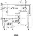
- the system 100generally comprises a block (or circuit) 102 and a block (or circuit) 104 .
- the circuit 102may be implemented as an electrically programmable read only memory module (EPROM) (or circuit). Other nonvolatile memories (e.g., EEPROM, flash memory, etc.) may also be implemented.
- the circuit 104may be implemented as a processor module (or circuit).
- the system 100may be used to test an external memory or other design (e.g., the memory devices 60 a - 60 n ).
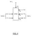
- the system 100may have an input 110 that may receive a signal (e.g., CLK), an input 112 that may receive a signal (e.g., IF), an input 114 that may receive a signal (e.g., EN), an output 116 that may present a signal (e.g., VALID), an output 118 that may present a signal (e.g., DATA), an output 120 that may present a signal (e.g., COM_TYPE), and an output 122 that may present a signal (e.g., PAR_TYPE).
- a signale.g., CLK
- an input 112that may receive a signal
- an input 114that may receive a signal (e.g., EN)
- an output 116that may present a signal
- an output 118that may present a signal
- DATAe.g., DATA
- an output 120that may present a signal
- an output 122that may present a signal (e.g., PAR_
- the circuit 102may have an input 130 that may receive the signal EN, an input 132 that may receive the signal CLK, an input 134 that may receive a signal (e.g., RA), and an output 136 that may present a signal (e.g., DO).
- the processor module 104may have an input 140 that may receive a signal EN, an input 142 that may receive a signal IF, an input 144 that may receive the signal CLK, an output 146 that may present the signal RA, and an input 148 that may receive the signal DO.
- the system 100may include a program stored in the EPROM module 102 .
- the processor module 104may read the program stored in the EPROM module 102 and interpret commands received from the program.
- the signal ENmay be implemented as an enable signal.
- the signal IFmay be implemented as an interface signal.
- the signal CLKmay be implemented as a clock signal that oscillates at a particular frequency.
- the signal RAmay be implemented as a read address signal.
- the signal DOmay be implemented as a data output signal.
- the circuit 102may be implemented as a programmable read-only memory (or ROM). However, other types of non-volatile memory circuits may be used to meet the design criteria of a particular implementation.
- the memory 102may be implemented as a binary table that may be hardwired as part of the controller 100 .
- the memory circuit 102may be implemented as a type of memory appropriate for use in cell-based chip designs for data storing along with the data read-only operation.
- the memory circuit 102may be used to store system-level programs.
- the memory circuit 102may be configured to download and change programs on the fly.
- the memory circuit 102may be implemented as a two port (or dual port) memory.
- One porte.g., a port A
- Another porte.g., a port B
- writinge.g., downloading
- a two port implementationmay be useful for built-in testing chip purposes.
- the processor circuit 104may be implemented as a built-in microprocessor.
- the circuit 104may be built into a memory test system.
- the microprocessor 104may be configured to read a sequence of data stored in the memory 102 .
- the datamay be read, in one example, one item at a time.
- the circuit 104generally comprises a circuit 150 , a circuit 152 , a circuit 154 , a circuit 156 , a circuit 158 , and a circuit 160 .
- the circuits 150 , 152 and 154may be implemented as flip-flops.
- the circuit 156may be implemented as an adder circuit.
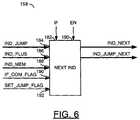
- the circuit 158may be implemented as a NEXT IND circuit.
- the circuit 160may be implemented as a flag circuit.
- the circuit 156may generate a signal (e.g., IND_PLUS).
- the circuit 152may generate a signal (e.g., IND_JUMP).
- the circuit 154may generate a signal (e.g., VALID).
- the flip-flops 150 , 152 and 154may store and retrieve current values of IND, IND_JUMP and EN.
- the flip-flops 150 , 152 and 154may also provide a one (or more) clock cycle delay to the value of the read address signal RA, the value of the signal IND JUMP, and the value of the enable input signal EN.
- the circuit 158may have an input 180 that may receive the signal VALID, an input 182 that may receive the signal IF, an input 184 that may receive the signal IND_JUMP, an input 186 that may receive the signal IND_PLUS, an input 188 that may receive a signal (e.g., IND_MEM), an input 190 that may receive a signal (e.g., IF_COM_FLAG), and an input 192 that may receive a signal (e.g., SET_JUMP_FLAG).
- the signal IF_COM_FLAG and the signal SET_JUMP_FLAGmay be implemented as auxiliary flags.
- the signal DOmay be stored in the memory 102 .
- the signal DOmay have a specific format that may be used for testing.
- the data signal DOmay be implemented as a microprocessor command and two prefix bits.
- the prefix bits PREF 0 and PREF 1may be implemented to code the microprocessor command as one of the following types:
- the circuit 158may compute the next value of the signal IND (e.g., the memory address RA to be read next), IND NEXT, and the next value for the signal IND_JUMP, IND JUMP NEXT.
- INDe.g., the memory address RA to be read next
- IND NEXTe.g., the next value for the signal IND_JUMP, IND JUMP NEXT.
- the circuit 158computes new values for the signal IND_NEXT and the signal IND_JUMP_NEXT as follows:
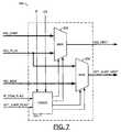
- the circuit 158generally comprises a circuit 202 , a circuit 204 , and a circuit 206 .
- the circuit 202may be implemented as a multiplexer.
- the circuit 204may be implemented as a de-multiplexer.
- the circuit 206may be implemented as a multiplexer.
- the circuits 202 , 204 and 206illustrate an example implementation of the logic described. Other logic may be implemented to meet the design criteria of a particular design.
- the circuit 220may be implemented as a command interpreter.
- the command interpreter 220may be configured to receive the signals COM_TYPE, PAR_TYPE, DATA, and VALID.
- the signal DATAgenerated from the test controller module 100 , includes the microprocessor data and commands that may be further interpreted and decoded by the command interpreter circuit 220 .
- the test controller 100may present the signal DATA to be decoded by the command interpreter 220 .
- the command interpreter 220generates test command-data flow as the signal TEST_DATA.
- the various signals of the present inventionare generally “on” (e.g., a digital HIGH, or 1) or “off” (e.g., a digital LOW, or 0).
- the particular polarities of the on (e.g., asserted) and off (e.g., de-asserted) states of the signalsmay be adjusted (e.g., reversed) to meet the design criteria of a particular implementation.
- invertersmay be added to change a particular polarity of the signals.
Landscapes
- Engineering & Computer Science (AREA)
- General Engineering & Computer Science (AREA)
- Physics & Mathematics (AREA)
- General Physics & Mathematics (AREA)
- Tests Of Electronic Circuits (AREA)
Abstract
Description
Capacity =2IND—WIDTH,
where the signal DO is 2-bits wider than the memory address signal RA. If the first two most significant bits are denoted as a prefix bit (e.g., PREF0) and a prefix bit (e.g., PREF1), then the signal DO may be defined as follows:
DO =(PREF0, PREF1, DATA),
where DATA is a binary word having a width defined as IND WIDTH bits. In one example, the data signal DO may be implemented as a microprocessor command and two prefix bits. The prefix bits PREF0and PREF1, may be implemented to code the microprocessor command as one of the following types:
Capacity=16÷128.
Claims (20)
Priority Applications (1)
| Application Number | Priority Date | Filing Date | Title |
|---|---|---|---|
| US12/118,477US7882406B2 (en) | 2008-05-09 | 2008-05-09 | Built in test controller with a downloadable testing program |
Applications Claiming Priority (1)
| Application Number | Priority Date | Filing Date | Title |
|---|---|---|---|
| US12/118,477US7882406B2 (en) | 2008-05-09 | 2008-05-09 | Built in test controller with a downloadable testing program |
Publications (2)
| Publication Number | Publication Date |
|---|---|
| US20090282303A1 US20090282303A1 (en) | 2009-11-12 |
| US7882406B2true US7882406B2 (en) | 2011-02-01 |
Family
ID=41267874
Family Applications (1)
| Application Number | Title | Priority Date | Filing Date |
|---|---|---|---|
| US12/118,477Expired - Fee RelatedUS7882406B2 (en) | 2008-05-09 | 2008-05-09 | Built in test controller with a downloadable testing program |
Country Status (1)
| Country | Link |
|---|---|
| US (1) | US7882406B2 (en) |
Cited By (1)
| Publication number | Priority date | Publication date | Assignee | Title |
|---|---|---|---|---|
| US20160307644A1 (en)* | 2013-12-03 | 2016-10-20 | SK Hynix Inc. | Built-in self-test circuit and semiconductor device including the same |
Families Citing this family (3)
| Publication number | Priority date | Publication date | Assignee | Title |
|---|---|---|---|---|
| KR101877939B1 (en)* | 2012-03-15 | 2018-08-10 | 에스케이하이닉스 주식회사 | Test circuit, memory system and test method of memory system |
| JP6478562B2 (en) | 2013-11-07 | 2019-03-06 | 株式会社半導体エネルギー研究所 | Semiconductor device |
| US9711241B2 (en)* | 2015-04-01 | 2017-07-18 | Qualcomm Incorporated | Method and apparatus for optimized memory test status detection and debug |
Citations (46)
| Publication number | Priority date | Publication date | Assignee | Title |
|---|---|---|---|---|
| US4517512A (en) | 1982-05-24 | 1985-05-14 | Micro Component Technology, Inc. | Integrated circuit test apparatus test head |
| US4929889A (en) | 1988-06-13 | 1990-05-29 | Digital Equipment Corporation | Data path chip test architecture |
| US5051997A (en)* | 1987-12-17 | 1991-09-24 | Mitsubishi Denki Kabushiki Kaisha | Semiconductor integrated circuit with self-test function |
| US5617531A (en) | 1993-11-02 | 1997-04-01 | Motorola, Inc. | Data Processor having a built-in internal self test controller for testing a plurality of memories internal to the data processor |
| US5742557A (en) | 1996-06-20 | 1998-04-21 | Northern Telecom Limited | Multi-port random access memory |
| US5896330A (en) | 1996-06-20 | 1999-04-20 | Northern Telecom Limited | Multi-port random access memory with shadow write test mode |
| US5961653A (en) | 1997-02-19 | 1999-10-05 | International Business Machines Corporation | Processor based BIST for an embedded memory |
| US6014336A (en)* | 1997-04-30 | 2000-01-11 | Texas Instruments Incorporated | Test enable control for built-in self-test |
| US6070256A (en) | 1997-05-29 | 2000-05-30 | Nortel Networks Corporation | Method and apparatus for self-testing multi-port RAMs |
| US6085334A (en) | 1998-04-17 | 2000-07-04 | Motorola, Inc. | Method and apparatus for testing an integrated memory device |
| US6347056B1 (en) | 2001-05-16 | 2002-02-12 | Motorola, Inc. | Recording of result information in a built-in self-test circuit and method therefor |
| US6353563B1 (en) | 1996-04-30 | 2002-03-05 | Texas Instruments Incorporated | Built-in self-test arrangement for integrated circuit memory devices |
| US20020059543A1 (en) | 2000-11-13 | 2002-05-16 | Wu-Tung Cheng | Full-speed bist controller for testing embedded synchronous memories |
| US20020104051A1 (en)* | 2001-01-31 | 2002-08-01 | Stmicroelectronics, Inc. | Embedded field programmable gate array for performing built-in self test functions in a system on a chip and method of operation |
| US20020129298A1 (en) | 2001-03-09 | 2002-09-12 | Mitsubishi Denki Kabushiki Kaisha | Method of and apparatus for testing CPU built-in RAM mixed LSI |
| US20020174394A1 (en) | 2001-05-16 | 2002-11-21 | Ledford James S. | External control of algorithm execution in a built-in self-test circuit and method therefor |
| US20020178416A1 (en) | 2001-05-23 | 2002-11-28 | Ibm Corporation | Hierarchical built-in self-test for system-on-chip design |
| US20020188902A1 (en) | 2001-03-20 | 2002-12-12 | Daniel Fan | Test system algorithmic program generators |
| US20020194545A1 (en) | 2001-04-27 | 2002-12-19 | Abbott Robert A. | Method of testing embedded memory array and embedded memory controller for use therewith |
| US20030023914A1 (en) | 2001-07-30 | 2003-01-30 | Taylor Richard D. | Built-in-self-test using embedded memory and processor in an application specific integrated circuit |
| US6553526B1 (en) | 1999-11-08 | 2003-04-22 | International Business Machines Corporation | Programmable array built-in self test method and system for arrays with imbedded logic |
| US6634003B1 (en) | 2000-02-10 | 2003-10-14 | Lsi Logic Corporation | Decoding circuit for memories with redundancy |
| US6681358B1 (en) | 2000-02-22 | 2004-01-20 | Lsi Logic Corporation | Parallel testing of a multiport memory |
| US20040181303A1 (en) | 2002-12-02 | 2004-09-16 | Silverbrook Research Pty Ltd | Relatively unique ID in integrated circuit |
| US20050015671A1 (en) | 2003-06-30 | 2005-01-20 | Sun Microsystems, Inc. A Delaware Corporation | On-chip testing of embedded memories using Address Space Identifier bus in SPARC architectures |
| US20050028058A1 (en)* | 2003-07-30 | 2005-02-03 | Martin Perner | Semiconductor circuit and method for testing, monitoring and application-near setting of a semiconductor circuit |
| US20050138514A1 (en)* | 2003-12-04 | 2005-06-23 | International Business Machines Corporation | ABIST-assisted detection of scan chain defects |
| US6941494B1 (en) | 2001-12-21 | 2005-09-06 | Lsi Logic Corporation | Built-in test for multiple memory circuits |
| US20050246602A1 (en)* | 2004-04-08 | 2005-11-03 | Stmicroelectronics Pvt. Ltd. | On-chip and at-speed tester for testing and characterization of different types of memories |
| US20050262401A1 (en) | 2004-04-21 | 2005-11-24 | Nec Electronics Corporation | Central processing unit and micro computer |
| US20050268159A1 (en) | 2001-12-31 | 2005-12-01 | Broadcom Corporation | System and method of improving memory yield in frame buffer memory using failing memory location |
| US7010736B1 (en) | 2002-07-22 | 2006-03-07 | Advanced Micro Devices, Inc. | Address sequencer within BIST (Built-in-Self-Test) system |
| US7028240B1 (en)* | 2002-07-22 | 2006-04-11 | Advanced Micro Devices, Inc. | Diagnostic mode for testing functionality of BIST (built-in-self-test) back-end state machine |
| US7062694B2 (en)* | 2003-02-07 | 2006-06-13 | Sun Microsystems, Inc. | Concurrently programmable dynamic memory built-in self-test (BIST) |
| US20060156134A1 (en) | 2004-11-18 | 2006-07-13 | Nilanjan Mukherjee | Programmable memory built-in-self-test (MBIST) method and apparatus |
| US7096386B2 (en) | 2002-09-19 | 2006-08-22 | Oki Electric Industry Co., Ltd. | Semiconductor integrated circuit having functional modules each including a built-in self testing circuit |
| US20060212765A1 (en) | 2005-03-14 | 2006-09-21 | Juerg Haufe | Integrated circuit with a control input that can be disabled |
| US20060242521A1 (en)* | 1997-04-30 | 2006-10-26 | Hii Kuong H | Built-in self-test arrangement for integrated circuit memory devices |
| US7139204B1 (en) | 2004-06-07 | 2006-11-21 | Virage Logic Corporation | Method and system for testing a dual-port memory at speed in a stressed environment |
| US7260759B1 (en) | 2004-06-16 | 2007-08-21 | Sun Microsystems, Inc. | Method and apparatus for an efficient memory built-in self test architecture for high performance microprocessors |
| US20070220389A1 (en)* | 2006-02-27 | 2007-09-20 | Hitachi, Ltd. | Integrated circuit device, diagnosis method and diagnosis circuit for the same |
| US20080077834A1 (en) | 2006-09-27 | 2008-03-27 | Ajay Khoche | Deterministic Diagnostic Information Capture from Memory Devices with Built-in Self Test |
| US20080282119A1 (en)* | 2006-10-24 | 2008-11-13 | Takahiro Suzuki | Memory device and built in self-test method of the same |
| US20090133003A1 (en) | 2007-11-21 | 2009-05-21 | Lsi Corporation | Command language for memory testing |
| US7653854B2 (en) | 2006-07-07 | 2010-01-26 | Kabushiki Kaisha Toshiba | Semiconductor integrated circuit having a (BIST) built-in self test circuit for fault diagnosing operation of a memory |
| US7773439B2 (en) | 2006-04-13 | 2010-08-10 | Hynix Semiconductor Inc. | Test operation of multi-port memory device |
- 2008
- 2008-05-09USUS12/118,477patent/US7882406B2/ennot_activeExpired - Fee Related
Patent Citations (47)
| Publication number | Priority date | Publication date | Assignee | Title |
|---|---|---|---|---|
| US4517512A (en) | 1982-05-24 | 1985-05-14 | Micro Component Technology, Inc. | Integrated circuit test apparatus test head |
| US5051997A (en)* | 1987-12-17 | 1991-09-24 | Mitsubishi Denki Kabushiki Kaisha | Semiconductor integrated circuit with self-test function |
| US4929889A (en) | 1988-06-13 | 1990-05-29 | Digital Equipment Corporation | Data path chip test architecture |
| US5617531A (en) | 1993-11-02 | 1997-04-01 | Motorola, Inc. | Data Processor having a built-in internal self test controller for testing a plurality of memories internal to the data processor |
| US6353563B1 (en) | 1996-04-30 | 2002-03-05 | Texas Instruments Incorporated | Built-in self-test arrangement for integrated circuit memory devices |
| US6288969B1 (en) | 1996-06-20 | 2001-09-11 | Nortel Networks Limited | Multi-port random access memory |
| US5742557A (en) | 1996-06-20 | 1998-04-21 | Northern Telecom Limited | Multi-port random access memory |
| US5896330A (en) | 1996-06-20 | 1999-04-20 | Northern Telecom Limited | Multi-port random access memory with shadow write test mode |
| US5961653A (en) | 1997-02-19 | 1999-10-05 | International Business Machines Corporation | Processor based BIST for an embedded memory |
| US6014336A (en)* | 1997-04-30 | 2000-01-11 | Texas Instruments Incorporated | Test enable control for built-in self-test |
| US20060242521A1 (en)* | 1997-04-30 | 2006-10-26 | Hii Kuong H | Built-in self-test arrangement for integrated circuit memory devices |
| US6070256A (en) | 1997-05-29 | 2000-05-30 | Nortel Networks Corporation | Method and apparatus for self-testing multi-port RAMs |
| US6085334A (en) | 1998-04-17 | 2000-07-04 | Motorola, Inc. | Method and apparatus for testing an integrated memory device |
| US6553526B1 (en) | 1999-11-08 | 2003-04-22 | International Business Machines Corporation | Programmable array built-in self test method and system for arrays with imbedded logic |
| US6634003B1 (en) | 2000-02-10 | 2003-10-14 | Lsi Logic Corporation | Decoding circuit for memories with redundancy |
| US6681358B1 (en) | 2000-02-22 | 2004-01-20 | Lsi Logic Corporation | Parallel testing of a multiport memory |
| US20020059543A1 (en) | 2000-11-13 | 2002-05-16 | Wu-Tung Cheng | Full-speed bist controller for testing embedded synchronous memories |
| US20020104051A1 (en)* | 2001-01-31 | 2002-08-01 | Stmicroelectronics, Inc. | Embedded field programmable gate array for performing built-in self test functions in a system on a chip and method of operation |
| US20020129298A1 (en) | 2001-03-09 | 2002-09-12 | Mitsubishi Denki Kabushiki Kaisha | Method of and apparatus for testing CPU built-in RAM mixed LSI |
| US20020188902A1 (en) | 2001-03-20 | 2002-12-12 | Daniel Fan | Test system algorithmic program generators |
| US20020194545A1 (en) | 2001-04-27 | 2002-12-19 | Abbott Robert A. | Method of testing embedded memory array and embedded memory controller for use therewith |
| US6347056B1 (en) | 2001-05-16 | 2002-02-12 | Motorola, Inc. | Recording of result information in a built-in self-test circuit and method therefor |
| US20020174394A1 (en) | 2001-05-16 | 2002-11-21 | Ledford James S. | External control of algorithm execution in a built-in self-test circuit and method therefor |
| US20020178416A1 (en) | 2001-05-23 | 2002-11-28 | Ibm Corporation | Hierarchical built-in self-test for system-on-chip design |
| US20030023914A1 (en) | 2001-07-30 | 2003-01-30 | Taylor Richard D. | Built-in-self-test using embedded memory and processor in an application specific integrated circuit |
| US6941494B1 (en) | 2001-12-21 | 2005-09-06 | Lsi Logic Corporation | Built-in test for multiple memory circuits |
| US20050268159A1 (en) | 2001-12-31 | 2005-12-01 | Broadcom Corporation | System and method of improving memory yield in frame buffer memory using failing memory location |
| US7028240B1 (en)* | 2002-07-22 | 2006-04-11 | Advanced Micro Devices, Inc. | Diagnostic mode for testing functionality of BIST (built-in-self-test) back-end state machine |
| US7010736B1 (en) | 2002-07-22 | 2006-03-07 | Advanced Micro Devices, Inc. | Address sequencer within BIST (Built-in-Self-Test) system |
| US7096386B2 (en) | 2002-09-19 | 2006-08-22 | Oki Electric Industry Co., Ltd. | Semiconductor integrated circuit having functional modules each including a built-in self testing circuit |
| US20040181303A1 (en) | 2002-12-02 | 2004-09-16 | Silverbrook Research Pty Ltd | Relatively unique ID in integrated circuit |
| US7062694B2 (en)* | 2003-02-07 | 2006-06-13 | Sun Microsystems, Inc. | Concurrently programmable dynamic memory built-in self-test (BIST) |
| US20050015671A1 (en) | 2003-06-30 | 2005-01-20 | Sun Microsystems, Inc. A Delaware Corporation | On-chip testing of embedded memories using Address Space Identifier bus in SPARC architectures |
| US20050028058A1 (en)* | 2003-07-30 | 2005-02-03 | Martin Perner | Semiconductor circuit and method for testing, monitoring and application-near setting of a semiconductor circuit |
| US20050138514A1 (en)* | 2003-12-04 | 2005-06-23 | International Business Machines Corporation | ABIST-assisted detection of scan chain defects |
| US20050246602A1 (en)* | 2004-04-08 | 2005-11-03 | Stmicroelectronics Pvt. Ltd. | On-chip and at-speed tester for testing and characterization of different types of memories |
| US20050262401A1 (en) | 2004-04-21 | 2005-11-24 | Nec Electronics Corporation | Central processing unit and micro computer |
| US7139204B1 (en) | 2004-06-07 | 2006-11-21 | Virage Logic Corporation | Method and system for testing a dual-port memory at speed in a stressed environment |
| US7260759B1 (en) | 2004-06-16 | 2007-08-21 | Sun Microsystems, Inc. | Method and apparatus for an efficient memory built-in self test architecture for high performance microprocessors |
| US20060156134A1 (en) | 2004-11-18 | 2006-07-13 | Nilanjan Mukherjee | Programmable memory built-in-self-test (MBIST) method and apparatus |
| US20060212765A1 (en) | 2005-03-14 | 2006-09-21 | Juerg Haufe | Integrated circuit with a control input that can be disabled |
| US20070220389A1 (en)* | 2006-02-27 | 2007-09-20 | Hitachi, Ltd. | Integrated circuit device, diagnosis method and diagnosis circuit for the same |
| US7773439B2 (en) | 2006-04-13 | 2010-08-10 | Hynix Semiconductor Inc. | Test operation of multi-port memory device |
| US7653854B2 (en) | 2006-07-07 | 2010-01-26 | Kabushiki Kaisha Toshiba | Semiconductor integrated circuit having a (BIST) built-in self test circuit for fault diagnosing operation of a memory |
| US20080077834A1 (en) | 2006-09-27 | 2008-03-27 | Ajay Khoche | Deterministic Diagnostic Information Capture from Memory Devices with Built-in Self Test |
| US20080282119A1 (en)* | 2006-10-24 | 2008-11-13 | Takahiro Suzuki | Memory device and built in self-test method of the same |
| US20090133003A1 (en) | 2007-11-21 | 2009-05-21 | Lsi Corporation | Command language for memory testing |
Cited By (2)
| Publication number | Priority date | Publication date | Assignee | Title |
|---|---|---|---|---|
| US20160307644A1 (en)* | 2013-12-03 | 2016-10-20 | SK Hynix Inc. | Built-in self-test circuit and semiconductor device including the same |
| US9837171B2 (en)* | 2013-12-03 | 2017-12-05 | SK Hynix Inc. | Built-in self-test circuit and semiconductor device including the same |
Also Published As
| Publication number | Publication date |
|---|---|
| US20090282303A1 (en) | 2009-11-12 |
Similar Documents
| Publication | Publication Date | Title |
|---|---|---|
| KR101780422B1 (en) | Nonvolatile memory device, reading method thereof and memory system including the same | |
| US6845053B2 (en) | Power throughput adjustment in flash memory | |
| US20160034346A1 (en) | NAND Flash Memory Having Internal ECC Processing and Method of Operation Thereof | |
| US7710791B2 (en) | Input circuit of a non-volatile semiconductor memory device | |
| US20160034352A1 (en) | NAND Flash Memory Having an Enhanced Buffer Read Capability and Method of Operation Thereof | |
| CN101467213A (en) | NAND system with a data write frequency greater than a command-and-address-load frequency | |
| KR20170109026A (en) | Methods and Apparatus for Command Shifter Reduction | |
| US7882406B2 (en) | Built in test controller with a downloadable testing program | |
| JP4713143B2 (en) | Semiconductor memory device | |
| US9817065B2 (en) | Test mode circuit and semiconductor device including the same | |
| US9047956B2 (en) | Concurrent operation of plural flash memories | |
| JP2006155710A (en) | Semiconductor memory device | |
| US7733738B2 (en) | Semiconductor memory device and a data write and read method thereof | |
| US6538943B2 (en) | Method and apparatus to conditionally precharge a partitioned read-only memory with shared wordlines for low power operation | |
| US9001570B1 (en) | Pseudo retention till access mode enabled memory | |
| KR100733954B1 (en) | Flash memory device with improved scan structure | |
| JP5999097B2 (en) | Semiconductor integrated circuit and control method thereof | |
| US7436719B2 (en) | Auto-precharge signal generating circuit | |
| US20110119563A1 (en) | Semiconductor memory | |
| JP5032137B2 (en) | Semiconductor memory device | |
| US7330934B2 (en) | Cache memory with reduced power and increased memory bandwidth | |
| KR100996093B1 (en) | Nonvolatile Memory Device and Operation Method | |
| CN112863576B (en) | Word line bias voltage generation circuit for NAND flash memory | |
| JP2011243275A (en) | Semiconductor memory device and operation method for the same | |
| US7652905B2 (en) | Flash memory array architecture |
Legal Events
| Date | Code | Title | Description |
|---|---|---|---|
| AS | Assignment | Owner name:LSI CORPORATION, CALIFORNIA Free format text:ASSIGNMENT OF ASSIGNORS INTEREST;ASSIGNORS:ANDREEV, ALEXANDRE;BOLOTOV, ANATOLI;REEL/FRAME:020985/0594 Effective date:20080509 | |
| FEPP | Fee payment procedure | Free format text:PAYOR NUMBER ASSIGNED (ORIGINAL EVENT CODE: ASPN); ENTITY STATUS OF PATENT OWNER: LARGE ENTITY | |
| AS | Assignment | Owner name:DEUTSCHE BANK AG NEW YORK BRANCH, AS COLLATERAL AG Free format text:PATENT SECURITY AGREEMENT;ASSIGNORS:LSI CORPORATION;AGERE SYSTEMS LLC;REEL/FRAME:032856/0031 Effective date:20140506 | |
| FPAY | Fee payment | Year of fee payment:4 | |
| AS | Assignment | Owner name:AVAGO TECHNOLOGIES GENERAL IP (SINGAPORE) PTE. LTD Free format text:ASSIGNMENT OF ASSIGNORS INTEREST;ASSIGNOR:LSI CORPORATION;REEL/FRAME:035390/0388 Effective date:20140814 | |
| AS | Assignment | Owner name:LSI CORPORATION, CALIFORNIA Free format text:TERMINATION AND RELEASE OF SECURITY INTEREST IN PATENT RIGHTS (RELEASES RF 032856-0031);ASSIGNOR:DEUTSCHE BANK AG NEW YORK BRANCH, AS COLLATERAL AGENT;REEL/FRAME:037684/0039 Effective date:20160201 Owner name:AGERE SYSTEMS LLC, PENNSYLVANIA Free format text:TERMINATION AND RELEASE OF SECURITY INTEREST IN PATENT RIGHTS (RELEASES RF 032856-0031);ASSIGNOR:DEUTSCHE BANK AG NEW YORK BRANCH, AS COLLATERAL AGENT;REEL/FRAME:037684/0039 Effective date:20160201 | |
| AS | Assignment | Owner name:BANK OF AMERICA, N.A., AS COLLATERAL AGENT, NORTH CAROLINA Free format text:PATENT SECURITY AGREEMENT;ASSIGNOR:AVAGO TECHNOLOGIES GENERAL IP (SINGAPORE) PTE. LTD.;REEL/FRAME:037808/0001 Effective date:20160201 Owner name:BANK OF AMERICA, N.A., AS COLLATERAL AGENT, NORTH Free format text:PATENT SECURITY AGREEMENT;ASSIGNOR:AVAGO TECHNOLOGIES GENERAL IP (SINGAPORE) PTE. LTD.;REEL/FRAME:037808/0001 Effective date:20160201 | |
| AS | Assignment | Owner name:AVAGO TECHNOLOGIES GENERAL IP (SINGAPORE) PTE. LTD., SINGAPORE Free format text:TERMINATION AND RELEASE OF SECURITY INTEREST IN PATENTS;ASSIGNOR:BANK OF AMERICA, N.A., AS COLLATERAL AGENT;REEL/FRAME:041710/0001 Effective date:20170119 Owner name:AVAGO TECHNOLOGIES GENERAL IP (SINGAPORE) PTE. LTD Free format text:TERMINATION AND RELEASE OF SECURITY INTEREST IN PATENTS;ASSIGNOR:BANK OF AMERICA, N.A., AS COLLATERAL AGENT;REEL/FRAME:041710/0001 Effective date:20170119 | |
| FEPP | Fee payment procedure | Free format text:MAINTENANCE FEE REMINDER MAILED (ORIGINAL EVENT CODE: REM.); ENTITY STATUS OF PATENT OWNER: LARGE ENTITY | |
| AS | Assignment | Owner name:AVAGO TECHNOLOGIES INTERNATIONAL SALES PTE. LIMITE Free format text:MERGER;ASSIGNOR:AVAGO TECHNOLOGIES GENERAL IP (SINGAPORE) PTE. LTD.;REEL/FRAME:047642/0417 Effective date:20180509 | |
| AS | Assignment | Owner name:AVAGO TECHNOLOGIES INTERNATIONAL SALES PTE. LIMITE Free format text:CORRECTIVE ASSIGNMENT TO CORRECT THE EXECUTION DATE OF THE MERGER PREVIOUSLY RECORDED ON REEL 047642 FRAME 0417. ASSIGNOR(S) HEREBY CONFIRMS THE ASSIGNMENT,;ASSIGNOR:AVAGO TECHNOLOGIES GENERAL IP (SINGAPORE) PTE. LTD.;REEL/FRAME:048521/0395 Effective date:20180905 | |
| LAPS | Lapse for failure to pay maintenance fees | Free format text:PATENT EXPIRED FOR FAILURE TO PAY MAINTENANCE FEES (ORIGINAL EVENT CODE: EXP.); ENTITY STATUS OF PATENT OWNER: LARGE ENTITY | |
| STCH | Information on status: patent discontinuation | Free format text:PATENT EXPIRED DUE TO NONPAYMENT OF MAINTENANCE FEES UNDER 37 CFR 1.362 | |
| FP | Lapsed due to failure to pay maintenance fee | Effective date:20190201 |