US7881355B2 - System and method for generating intense laser light from laser diode arrays - Google Patents
System and method for generating intense laser light from laser diode arraysDownload PDFInfo
- Publication number
- US7881355B2 US7881355B2US11/300,726US30072605AUS7881355B2US 7881355 B2US7881355 B2US 7881355B2US 30072605 AUS30072605 AUS 30072605AUS 7881355 B2US7881355 B2US 7881355B2
- Authority
- US
- United States
- Prior art keywords
- laser
- optical
- columns
- laser light
- fast
- Prior art date
- Legal status (The legal status is an assumption and is not a legal conclusion. Google has not performed a legal analysis and makes no representation as to the accuracy of the status listed.)
- Active - Reinstated, expires
Links
Images


Classifications
- H—ELECTRICITY
- H01—ELECTRIC ELEMENTS
- H01S—DEVICES USING THE PROCESS OF LIGHT AMPLIFICATION BY STIMULATED EMISSION OF RADIATION [LASER] TO AMPLIFY OR GENERATE LIGHT; DEVICES USING STIMULATED EMISSION OF ELECTROMAGNETIC RADIATION IN WAVE RANGES OTHER THAN OPTICAL
- H01S5/00—Semiconductor lasers
- H01S5/40—Arrangement of two or more semiconductor lasers, not provided for in groups H01S5/02 - H01S5/30
- H01S5/4025—Array arrangements, e.g. constituted by discrete laser diodes or laser bar
- H01S5/4031—Edge-emitting structures
- H01S5/4043—Edge-emitting structures with vertically stacked active layers
- H01S5/405—Two-dimensional arrays
- G—PHYSICS
- G02—OPTICS
- G02B—OPTICAL ELEMENTS, SYSTEMS OR APPARATUS
- G02B19/00—Condensers, e.g. light collectors or similar non-imaging optics
- G02B19/0004—Condensers, e.g. light collectors or similar non-imaging optics characterised by the optical means employed
- G02B19/0009—Condensers, e.g. light collectors or similar non-imaging optics characterised by the optical means employed having refractive surfaces only
- G02B19/0014—Condensers, e.g. light collectors or similar non-imaging optics characterised by the optical means employed having refractive surfaces only at least one surface having optical power
- G—PHYSICS
- G02—OPTICS
- G02B—OPTICAL ELEMENTS, SYSTEMS OR APPARATUS
- G02B19/00—Condensers, e.g. light collectors or similar non-imaging optics
- G02B19/0033—Condensers, e.g. light collectors or similar non-imaging optics characterised by the use
- G02B19/0047—Condensers, e.g. light collectors or similar non-imaging optics characterised by the use for use with a light source
- G02B19/0052—Condensers, e.g. light collectors or similar non-imaging optics characterised by the use for use with a light source the light source comprising a laser diode
- G02B19/0057—Condensers, e.g. light collectors or similar non-imaging optics characterised by the use for use with a light source the light source comprising a laser diode in the form of a laser diode array, e.g. laser diode bar
- G—PHYSICS
- G02—OPTICS
- G02B—OPTICAL ELEMENTS, SYSTEMS OR APPARATUS
- G02B27/00—Optical systems or apparatus not provided for by any of the groups G02B1/00 - G02B26/00, G02B30/00
- G02B27/09—Beam shaping, e.g. changing the cross-sectional area, not otherwise provided for
- G02B27/0938—Using specific optical elements
- G02B27/095—Refractive optical elements
- G02B27/0955—Lenses
- G02B27/0961—Lens arrays
- G—PHYSICS
- G02—OPTICS
- G02B—OPTICAL ELEMENTS, SYSTEMS OR APPARATUS
- G02B27/00—Optical systems or apparatus not provided for by any of the groups G02B1/00 - G02B26/00, G02B30/00
- G02B27/09—Beam shaping, e.g. changing the cross-sectional area, not otherwise provided for
- G02B27/0938—Using specific optical elements
- G02B27/095—Refractive optical elements
- G02B27/0955—Lenses
- G02B27/0966—Cylindrical lenses
- G—PHYSICS
- G02—OPTICS
- G02B—OPTICAL ELEMENTS, SYSTEMS OR APPARATUS
- G02B27/00—Optical systems or apparatus not provided for by any of the groups G02B1/00 - G02B26/00, G02B30/00
- G02B27/28—Optical systems or apparatus not provided for by any of the groups G02B1/00 - G02B26/00, G02B30/00 for polarising
- G02B27/283—Optical systems or apparatus not provided for by any of the groups G02B1/00 - G02B26/00, G02B30/00 for polarising used for beam splitting or combining
- G—PHYSICS
- G02—OPTICS
- G02B—OPTICAL ELEMENTS, SYSTEMS OR APPARATUS
- G02B6/00—Light guides; Structural details of arrangements comprising light guides and other optical elements, e.g. couplings
- G02B6/24—Coupling light guides
- G02B6/42—Coupling light guides with opto-electronic elements
- G02B6/4296—Coupling light guides with opto-electronic elements coupling with sources of high radiant energy, e.g. high power lasers, high temperature light sources
- H—ELECTRICITY
- H01—ELECTRIC ELEMENTS
- H01S—DEVICES USING THE PROCESS OF LIGHT AMPLIFICATION BY STIMULATED EMISSION OF RADIATION [LASER] TO AMPLIFY OR GENERATE LIGHT; DEVICES USING STIMULATED EMISSION OF ELECTROMAGNETIC RADIATION IN WAVE RANGES OTHER THAN OPTICAL
- H01S5/00—Semiconductor lasers
- H01S5/40—Arrangement of two or more semiconductor lasers, not provided for in groups H01S5/02 - H01S5/30
- H01S5/4012—Beam combining, e.g. by the use of fibres, gratings, polarisers, prisms
Definitions
- the present inventionrelates to lasers, and more particular to optical configurations to effectively couple the outputs of a plurality of individual laser elements, such as laser diodes, into optical fibers to provide high efficiency transmission of power through the optical fiber.
- semiconductor laser diodesmake them the ideal candidates for applications requiring concentrated and spectrally pure laser light sources.
- Applicationssuch as optical storage, low end printing and telecommunications that once used many different types of laser sources, now only use semiconductor laser diode sources once these diode laser sources with the required characteristics were successfully developed.
- the primary reason that semiconductor laser diodes have these very useful characteristicsis that the excited or pumped laser area can be made very small through the use of semiconductor fabrication techniques such as photolithography and epitaxial layer growth. Due to the small lasing area, the gain and optical intensity, which are the two main ingredients necessary for efficient conversion of excited atoms in the lasing medium to lasing photons, the efficiency of a laser diode can be very high.
- Brightnesscan either be defined in terms of its Lagrange invariant, the area of the emitting light source times the solid angle of the divergence of the light from the source, or in the case of Gaussian beams, the M2 parameter.
- NAnumerical aperture
- the need to scale the output of these semiconductor laser diodes to higher powers while maintaining beam qualityhas led to several approaches.
- the firstis the well understood and documented approach to use these laser diodes to pump a solid state gain material such as NdYAG.
- a solid state gain materialsuch as NdYAG.
- This approachwhat would be the lower brightness of an array of incoherent semiconductor laser diodes is converted to the near M 2 of 1.0 TEM oo output of the laser diode pumped solid state laser.
- Another approachis to fiber couple the output of many individual laser diodes or laser diode bars to cladding pump a rare earth doped fiber laser. Near diffraction limited M 2 values of ⁇ 1.1 have been achieved with power levels greater than 800 W in a Yb doped double clad fiber laser.
- the apparatus and method of the inventionwhich utilizes two-dimensional laser arrays, such as stacked laser diode bars, and effectively combines the output from each two-dimension laser arrays into one or more optical fibers to achieve the desired intensity and beam quality.
- the laser elementssuch as laser diodes
- the laser elementsare arranged in rows and columns, with the fast axes of the laser elements in the column direction, and the outputs of laser elements in each column of the array are combined and imaged into the entrance end of one optical fiber.
- a summed beam with the brightness in the fast axis direction substantially equal or close to the brightness in the slow axis directioncan be achieved, thus providing improved beam quality.
- the outputs of the two-dimensional lasers carried by optical fibersmay be combined by techniques including fiber combination and spectral combination to result in a high-power laser beam with good beam quality carried by an output optical fiber.
- the inventionprovides for the preservation of the brightness of individual emitters in a 2-D stacked array of laser diode bars and their efficient coupling into optical fiber.
- New structures for processing, steering, combining and focusing the individual emitters into optical fiberare disclosed.
- FIG. 1( a )is a schematic diagram that illustrates the geometry of a single, broad area semiconductor laser diode having fast and slow axes;
- FIG. 1( b )is a schematic drawing that illustrates a laser bar with comprising multiple broad area semiconductor laser diodes in a one-dimensional array
- FIG. 1( c )is schematic drawing that illustrates a two-dimensional laser array formed by stacking a plurality of laser bars of the type shown in FIG. 1( b );
- FIGS. 2( a ) and 2 ( b )are schematic drawings illustrate two views along the fast and slow axis, respectively, for an configuration where the arrangement of individual laser diodes is aligned as a column in the fast axis such that the direction of their far field outputs aligned parallel to one another;
- FIGS. 3( a ) and 3 ( b )schematic drawings that illustrate views of the fast and slow axes, respectively, of the beams of the individual emitters as they converge on the fiber entrance aperture.
- FIGS. 4( a ) and 4 ( b )are schematic drawings that illustrate views of the fast and slow axis, respectively, for combining the outputs from single laser diode array such as that in FIG. 1 ( b );
- FIG. 5is a schematic representation of the rotational transformation of the beams from the laser array of FIGS. 4( a ) and 4 ( b );
- FIGS. 6( a ) and 6 ( b )are schematic drawings that illustrate views of the fast and slow axes, respectively, for combining the outputs from a stack of laser diode arrays according to a first embodiment of the invention
- FIGS. 7( a ) and 7 ( b )schematic drawings that illustrate views of the fast and slow axes, respectively, for combining the outputs from a stack of laser diode arrays according to a second embodiment of the invention
- FIG. 8is a schematic drawing that illustrates a configuration for combining output beams from adjacent columns of beams by means of polarization combination
- FIGS. 9( a ) and 9 ( b )are schematic drawings that illustrate views of the fast and slow axes respectively, for the embodiment in FIGS. 7( a ) and 7 ( b ) with the insertion of the polarization combining assembly;
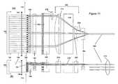
- FIG. 11is a schematic diagram that illustrates an alternative embodiment that utilizes polarization combination to combine output beams from columns of a 2-D laser array.
- the structure of a laser diode and the properties of its output lightis described first to facilitate an understanding and appreciation of the approach of the invention.
- the inventionis especially advantageous for combining the output beams from two-dimensional arrays of laser diodes to form an intense high-quality fiber-coupled beam.
- the present inventionis not limited to laser diodes, and can be applied to other forms of laser elements with a diffraction-limited small lasing area, including those that may be developed in the future.
- the term “group”is intended mean one or more contiguous columns in a laser array.
- FIG. 1( a )shows the typical geometry of a single broad area semiconductor laser diode 104 grown by epitaxial deposition.
- This deviceis characterized by an emitting or active region 100 of width y and thickness z and length x.
- This expitaxially grown and photolithographically defined regioncan be constructed in many different ways, but usually a single or multiple quantum well structure with an index guided waveguide in a material structure such as InGaAsP is a preferred embodiment.
- These devicesare further defined as having growth layers 108 , cleaved emitting facets 103 , and are mounted on a heat removing substrate, or heat sink 112 .
- the direction parallel to the semiconductor junctionis referred to the slow axis 116 .
- a stripe width yis defined photolithographically and the light emission from the aperture diverges in the far field 102 with the angle ⁇ defined at full width half max (FWHM).
- the direction perpendicular to the semiconductor junctionis referred to as the fast axis 118 .
- a stripe thickness zis defined epitaxially and the light emission from the aperture diverges in the far field 102 with the angle alpha ( ⁇ ) also defined at FWHM.
- zis around 1 micron and y is usually in the range of 50 to 200 microns and ⁇ is about 10 degrees while ⁇ is about 50 degrees.
- the M 2 in the slow axisvaries from 10 to 20 for these stripe dimensions and in the fast axis, the M 2 is near 1.
- FIG. 1( b )shows how a multiplicity of these broad area semiconductor laser diodes emitting regions 100 can be defined photolithographically to create a laser diode array bar 120 or multistripe bar.
- This multistripe bar 120has parallel electrical connections 124 to spread the high current load, and is mounted on a cooling substrate 128 , made up of either a conductive heat transfer plate, or a water cooled plate.
- a preferred embodiment for the cooling plate 128uses a microchannel cooling plate.
- the slow non-diffraction-limited direction 116can be defined as being parallel to the array of emitting regions 100
- the fast near-diffraction-limited direction 118can be defined as being perpendicular to the array of emitting regions 100 .
- FIG. 1( c )shows how a multiplicity of these multistripe bars 120 can be arranged to create a two-dimensional (“2-D”) stacked array 140 .
- the multistripe bars 120mounted on their cooling substrate 128 with their parallel electrical connections 124 , are placed with the multi stripe bars 120 aligned parallel to each other.
- This 2-D tacked array 140can be characterized as having a “row” or “row” direction 148 where the individual emitters 100 in each multistripe bar 120 all have their slow axis directions 116 aligned in the same plane.
- This 2-D Stacked Array 140can also be characterized as having a “column” or “column” direction 144 where columns individual emitters 100 in multiple multistripe bars 120 all have their fast axis directions 118 aligned in the same plane.
- the bars 120are mounted such the laser diodes in each column of the 2-D array 140 are aligned with each other, preferably with a tolerance of 5 microns or less, to prevent significant degradation of the quality of the beam generated by combining the outputs of the laser diodes, as described in greater detail below.
- Each 2-D stacked array 140may have 10 to 25 multistripe bars 120 and may generate output power in the range of 500 to 1500 Watts.
- Such a 2-D stacked array with columns and rows of laser diodes, with the fast axes of the laser diodes lined up along the column directions 144 and the slow axes of the laser diodes along the row directions 148 ,may be used as a building block to construct a system for high-brightness high-quality laser beam, as described in greater detail below.
- the outputs of the laser diodes in a 2-D arrayare effectively combined and coupled into one or more optical fibers to provide enhanced beam quality.
- the high-beam qualityis achieved by imaging the outputs from the laser diodes in a given column into one optical fiber.
- FIGS. 2( a ) and 2 ( b )shows the fast and slow axis views of a configuration where the laser diode emitters 104 are aligned in a column 144 with the direction of their far field outputs 102 parallel to each other.
- This column 144may be, for example, a column in the 2-D laser array shown in FIG.
- FIGS. 2( a ) and 2 ( b )for simplicity and clarity of illustration.
- all the laser diodes in such a column 144are arranged such that their fast axes align with the column direction.
- the laser diodes in a diode barsuch as the one shown in FIG. 1( b ) have their fast axes perpendicular to the longitudinal direction, or the row axis, of the laser bar.
- an optical assembly having multiple optical componentsis disposed between the laser diodes and the entrance end of the optical fiber.
- the fast and slow axis collimation optics 150 and 156collimate the output of the column of 104 in the fast 118 and slow 116 axis directions respectively. These are typically, though not limited to, cylindrical optics.
- the fast axis focusing and beam steering of the individual collimated beams 210are accomplished here through the use of a cylindrical optical assembly 230 of which the individual bundles of rays 210 passes through.
- This cylindrical optical assembly 230is a multi element optical device consisting of at a minimum a positive effective focal length cylindrical lens 214 followed by a negative effective focal length cylindrical lens 222 . Additional optical lenses 218 can be added between 214 and 222 for the reduction of aberrations.
- the output bundle of rays 226is passed through the slow axis focusing lens 164 into the multimode optical fiber 168 consisting of the desired diameter and NA.
- the use of the cylindrical optical assemblyaccomplishes the dual function of focusing the fast axis direction of each beam 116 to the appropriate waist diameter and steering the multiplicity of beams 226 to the appropriate NA for efficient coupling to optical fiber or other optical systems in a way the preserves the brightness of the original laser diode emitting regions 100 .
- FIGS. 2 a and bare designed such that it may be constructed using readily available lenses
- the combination of good beam quality and high intensity in a fiber-coupled laser beamis achieved by combining, into one optical fiber, the light outputs from laser diodes that form a column with their fast axes aligned with the column direction.
- the limiting brightness for the single laser emitting region 100is in the non diffraction limited slow axis direction 116 . This brightness is defined as the product of the laser stripe width y times the far field angular divergence ⁇ .
- the laser beams generated by a number of light sources 104 into an optical fibersuch that the brightness of the summed beams in the near diffraction limited fast axis direction 118 (the stripe thickness z times the far field angular divergence ⁇ ) is substantially equal or close to the brightness of the slow axis direction 116 .
- This arrangementcreates a Symmetric Brightness Unit (SBU) which preserves the brightness of the sum of the individual emitters 100 .
- the multimode fiber 168 of a desired diameter and NAis then chosen to match this SBU. Slightly increasing either the diameter of NA of 168 will work to lower the overall brightness of the SBU yet increase the efficiency of the fiber coupling.
- Optical aberrationssuch as Spherical aberration, coma, or variation in the mounting flatness of the laser diode bar 120 (referred to as “laser bar smile”) can decrease the overall brightness of the SBU and require a larger multimode fiber 168 diameter or NA for comparable coupling efficiency. While coupling into optical fiber is a desired embodiment, this technique can also be applied where the focused and process beams are then coupled into another optical system such as a materials processing optical system.
- FIGS. 3( a ) and 3 ( b )shows schematically in the fast and slow axes respectively how the beams from each of the laser diode emitters 104 forming the column of emitters 144 in FIGS. 2( a ) and 2 ( b ) converge at the multimode fiber optic 168 entrance face.
- the multimode fiber optic 168consists of a cladding layer 169 and a core 170 characterized by its diameter and acceptance angle 171 .
- the output bundle of beams 226comprising of the direction 102 for the beams from the individual laser diode emitters 104 are converging toward the multimode fiber optic 168 entrance face as each beam from each laser diode emitter is focused to the size optimal for coupling into the desired fiber dimensions 168 , and the multiplicity of laser diode emitters 144 is each steered at a different angle such that the bundle of beams is contained within the acceptance angle 171 of the multimode fiber 168 .
- the beams from the multiplicity of laser diode emitters 104 with their propagation directions 102overlap such that each beam is focused to the desired diameter and numerical aperture for the multimode fiber 168 . In this way, the creation of a SBU is created by transforming a laser diode source 104 of asymmetric brightness into a fiber of symmetric brightness.
- An SBU formed by combining the laser lights from one or more columns of laser diodes into an optical fibercan be combined with other fiber-coupled SBU from the same 2-D array to provide a high-intensity beam.
- the 2-D laser arraymay be used as a building block for a system for generating a high-brightness output laser beam.
- the number of 2-D laser arrays used in the systemmay depend on the desired output level, and the lights generated by laser diodes in the 2-D laser arrays may be combined through one or more combination stages to achieve the high-brightness output beam.
- FIG. 10shows an embodiment of a system comprising a multiplicity of fiber-coupled 2-D tacked arrays.
- This embodimentutilizes two techniques—fiber combination and spectral combination—to combine the laser lights from the multiple 2-D arrays into a final high-intensity output beam carried by an output fiber.
- a multi-fiber-coupled 2-D stacked array 300is constructed such that all of the emitters in the array emit light in a defined wavelength region 304 . Connections 308 are made to 300 for power and cooling as well as monitoring. Light from this multi fiber bundle 312 passes though a fiber combiner 316 to become a single fiber 320 .
- a fiber combiner 316can be, but is not limited to, a fused taper type device where the radius times NA product of the output fiber is in general equal to or greater than the sum of the radius times NA products of the input bundle.
- Such devicescan be purchased in standard or custom formats from companies like JDSU or Itf.
- a second multi fiber-coupled 2-D Stacked Array 324is constructed such that all of the emitters in its array emit light in a defined wavelength region 328 distinct from the first region 304 .
- the light from this multi fiber bundle 312also passes through its own fiber combiner 316 to become a single fiber 320 .
- a multiplicity of such multi fiber-coupled and fiber combined 2-D Stacked Arrayscan be created each having its own distinct wavelength region.
- the light from the multiplicity of fiber-coupled 2-D Stacked arrays 320is combined in wavelength in a spectral combiner 332 to produce a single fiber combined output. In this way, the laser light outputs of the multiple 2-D stacked arrays 300 are combined into one intense laser beam guided through the final output optical fiber.
- the spectral combiner 332is an optical wavelength multiplexing device whose single channel passband is designed to correspond to the defined wavelength region 304 that each mufti fiber-coupled 2-D Stacked Array 300 resides in.
- These spectral combiners 332can be constructed in a number of ways including yet not limited to: ruled gratings, volume Bragg holograms, thin film mirrors, prisms or fiber Bragg gratings. The designs and constructions of such combiners are well known.
- FIGS. 6( a ) and 6 ( b )shows the fast and slow axis views of the configuration of one embodiment for combining the outputs from a 2-D Stacked array 142 .
- the 2-D Stacked Array 142is formed by multistripe bars 120 of individual emitters 100 where the individual emitters 100 are aligned such that a row direction 148 consisting of a multiplicity of single emitters 100 is defined photolithographically on a single multistripe bar 120 .
- the multistripe bar 120is also aligned such that a column direction 144 is formed by a multiplicity of individual emitters 100 from a multiplicity of multistripe bars 120 .
- the 2-D Stacked array 142is aligned such that the individual emitters 100 lie on the surface of a cylinder of radius R whose length is the width of the individual multistripe bar 120 with the axis of propagation of light from each of the individual emitters 100 is directed to the center axis of the cylinder.
- Collimation in the fast 118 and slow axis 116is accomplished using multiple optical imaging elements.
- a single fast axis collimating cylindrical lens 180collimates the light from an entire row 148 , and each individual emitter has its own individual slow axis collimating lens 250 .
- the fast axis light from an entire row 148is focused to the appropriate beam dimension through a single fast axis focusing lens 254 .
- Slow axis collimated light and fast axis focused light from a multiplicity of single emitter beams 258 comprising the entire 2-D Stacked arrayis steered to the appropriate NA for the entire bundle of rays 266 through a single or assembly of cylindrical lenses 262 whose effective focal length is negative.
- Each column 144is then slow axis focused through a single cylindrical lens 164 to the desired diameter and NA, and then each column 144 is coupled to an individual optical fiber 168 .
- the diameter and NA of this fiberis chosen to match the brightness of the resulting SBU based on the optical processing of a column of single emitters 144 .
- the fiber-coupled output from the entire 2-D stacked array 142is consists of a bundle of optical fibers 312 where there is a 1:1 correspondence between the number of optical fibers 168 , and the number of columns 144 in the array. It should be noted that this embodiment represents one way of accomplishing this objective.
- optical elementscan be added with slow or fast axis power, or both, it improve optical performance, i.e., reduce aberrations, at the cost of optical efficiency.
- output light from this systemneed not be exclusively coupled into optical fibers.
- the output light from this systemcould also be coupled in to a number of different optical systems.
- FIGS. 7( a ) and 7 ( b )shows the fast and slow axis views of an alternate embodiment for combining the outputs from a 2-D Stacked array 140 .
- the 2-D Stacked Array 140consisting of multistripe bars 120 of individual emitters 100 where the individual emitters 100 are aligned such that a row or row direction 148 consisting of a multiplicity of single emitters 100 is defined photolithographically on a single multistripe bar 120 .
- the multistripe bars 120are also aligned such that a column or column direction 144 is formed by a multiplicity of individual emitters 100 from a multiplicity of multistripe bars 120 .
- the 2-D Stacked array 140is aligned such that the individual emitters 102 direction of propagation is parallel to all of the other single emitters 100 .
- Collimation in the fast 118 and slow axis 116is accomplished as follows: A single fast axis collimating cylindrical lens 180 collimates the light from an entire row 144 , and a single slow axis collimating cylindrical lens 184 collimates the light from an entire column 148 .
- a collimated beam 210is the result.
- the fast axis light from the entire 2-D Stacked Array 140is focused to the appropriate beam dimension and NA through the use of a Cylindrical Optical Assembly 230 .
- the Cylindrical Optical Assemblyis a multi element optical assembly consisting of at a minimum a positive effective focal length cylindrical lens 214 followed negative effective focal length cylindrical lens 220 . Additional positive and negative lenses 218 can be added between 214 and 222 to reduce optical aberrations.
- each emitter 100is fast axis focused to the appropriate dimension and the entire bundle of rays 226 has the desired NA for efficient coupling to optical fiber 168 or other types of optical systems.
- Each column 144is then slow axis focused through a single cylindrical lens 164 to the desired diameter and NA, and then each column 144 is coupled to an individual optical fiber 168 .
- Additional slow axis cylindrical lensesmay be incorporated into the design to act as relay lenses to keep the slow axis beam diameter within the boundaries defined by each column.
- the diameter and NA of this fiberis chosen to match the brightness of the resulting SBU based on the optical processing of a column of single emitters 100 .
- the fiber-coupled output from the entire 2-D stacked array 100is consists of a bundle of optical fibers 312 where there is a 1:1 correspondence between the number of optical fibers 168 , and the number of columns 144 in the array. It should be noted that this embodiment represents one way of accomplishing this objective. Additional optical elements can be added with slow or fast axis power, or both, it improve optical performance, i.e., reduce aberrations, at the cost of optical efficiency. In addition the output light from this system need not be exclusively coupled into optical fibers. The output light from this system could also be coupled in to a number of different optical systems.
- FIG. 8shows the slow axis direction 116 of a polarization combining structure 158 consisting of a substrate of a birefringent material 150 such a calcite or Yttrium Vanadate YVO4 oriented in the configurations as a displacement prism.
- a polarization combining structure 158consisting of a substrate of a birefringent material 150 such as calcite or Yttrium Vanadate YVO4 oriented in the configurations as a displacement prism.
- a birefringent material 150such as calcite or Yttrium Vanadate YVO4
- input beams of orthogonal polarizationsare combined into a single beam.
- the thickness L of the displacement prism for a material such a calciteis determined by the incoming separation of the input beams of distance P.
- an array of half wave plates 154 oriented 45 degrees to the incoming plane of polarizationplaced in an array adjacent to the displacement prism 150 .
- the half wave plates 154are placed so as to affect every other column of laser diode beams.
- Air or glass spacers 153are placed in the other column locations for no polarization rotation. In this configuration the polarization of the beams in say the odd columns are rotated 90 degrees 159 relative to their original orientation.
- adjacent columns of beamspass through the birefringent material, one polarization passes through unaffected while the other is refracted at an angle determined by the orientation and birefringent properties of the material.
- the thickness of the materialis chosen such that at the output of adjacent columns of beams are superimposed to form a combined output 160 traveling in a collinear direction.
- This element in the beam trainthe lights from two adjacent columns are combined and imaged into one optical fiber.
- This polarization combining structurecan be placed anywhere in the beam path, but is preferably placed at a location where the divergence of the individual beams is at a minimum.
- FIGS. 9( a ) and 9 ( b )shows an embodiment similar to that depicted in FIGS. 7( a ) and 7 ( b ) but contains the polarization combining assembly 158 placed in the collimated region of the beam paths.
- the output fiber bundle 312contains half the number of fibers as the configuration in FIGS. 7( a ) and 7 ( b ).
- FIGS. 11( a ) and 11 ( b )shows the fast and slow axis views of another alternate embodiment for combining the output beams of a 2-D Stacked array 140 .
- the 2-D Stacked Array 140has a plurality of multistripe bars 120 of individual emitters 100 , with the individual emitters 100 aligned such that a row or row direction 148 consisting of a multiplicity of single emitters 100 is defined photolithographically on a single multistripe bar 120 .
- the multistripe bars 120are also aligned such that a column or column direction 144 is formed by a multiplicity of individual emitters 100 from a multiplicity of multistripe bars 120 .
- the 2-D Stacked array 140is aligned such that the individual emitters 102 direction of propagation is parallel to all of the other single emitters 100 .
- Additional positive and negative lenses 218can be added between 214 and 222 to reduce optical aberrations.
- the light from each emitter 100is fast axis focused to the appropriate dimension and the entire bundle of rays 226 has the desired NA for efficient coupling to optical fiber 168 or other types of optical systems.
- the two adjacent, collimated columnsare then focused together using a slow axis focusing cylindrical lens 165 into one fiber 168 with the desired diameter and Numerical Aperture.
- the number of required fibers 313is thus again reduced in half, similar to that in the embodiment of FIG. 9 .
- This multicolumn focusing techniquecan also be applied to more than two columns. For instance, groups with three or more columns may be combined using this technique.
- FIGS. 4( a ) and 4 ( b )shows the fast and slow axis views of an alternative embodiment for combining the outputs from s single multistripe laser diode bar 120 .
- FIG. 5shows schematically this transformation from the row direction 100 to the column direction 100 through the rotational array 100 .
- This cylindrical optical assembly 192is a multi element optical device consisting of at a minimum a positive effective focal length cylindrical lens 194 followed by a negative effective focal length cylindrical lens 198 . Additional optical lenses 202 can be added between 194 and 198 for the reduction of aberrations. An additional lens 206 focuses the slow axis direction to the appropriate beam size and NA to match the multimode fiber 208 .
Landscapes
- Physics & Mathematics (AREA)
- General Physics & Mathematics (AREA)
- Optics & Photonics (AREA)
- Condensed Matter Physics & Semiconductors (AREA)
- Electromagnetism (AREA)
- Optical Couplings Of Light Guides (AREA)
- Semiconductor Lasers (AREA)
Abstract
Description
n=(y×θ)/(z×α)
Claims (18)
Priority Applications (5)
| Application Number | Priority Date | Filing Date | Title |
|---|---|---|---|
| US11/300,726US7881355B2 (en) | 2005-12-15 | 2005-12-15 | System and method for generating intense laser light from laser diode arrays |
| JP2008545615AJP2009520353A (en) | 2005-12-15 | 2006-11-22 | System and method for generating intense laser light from a laser diode array |
| EP06838278.7AEP1972043B1 (en) | 2005-12-15 | 2006-11-22 | System and method for generating intense laser light from laser diode arrays |
| PCT/US2006/045210WO2007078456A1 (en) | 2005-12-15 | 2006-11-22 | System and method for generating intense laser light from laser diode arrays |
| US13/004,620US8767790B2 (en) | 2005-12-15 | 2011-01-11 | System and method for generating intense laser light from laser diode arrays |
Applications Claiming Priority (1)
| Application Number | Priority Date | Filing Date | Title |
|---|---|---|---|
| US11/300,726US7881355B2 (en) | 2005-12-15 | 2005-12-15 | System and method for generating intense laser light from laser diode arrays |
Related Child Applications (1)
| Application Number | Title | Priority Date | Filing Date |
|---|---|---|---|
| US13/004,620ContinuationUS8767790B2 (en) | 2005-12-15 | 2011-01-11 | System and method for generating intense laser light from laser diode arrays |
Publications (2)
| Publication Number | Publication Date |
|---|---|
| US20080101429A1 US20080101429A1 (en) | 2008-05-01 |
| US7881355B2true US7881355B2 (en) | 2011-02-01 |
Family
ID=37951665
Family Applications (2)
| Application Number | Title | Priority Date | Filing Date |
|---|---|---|---|
| US11/300,726Active - Reinstated2026-12-02US7881355B2 (en) | 2005-12-15 | 2005-12-15 | System and method for generating intense laser light from laser diode arrays |
| US13/004,620Active2026-01-25US8767790B2 (en) | 2005-12-15 | 2011-01-11 | System and method for generating intense laser light from laser diode arrays |
Family Applications After (1)
| Application Number | Title | Priority Date | Filing Date |
|---|---|---|---|
| US13/004,620Active2026-01-25US8767790B2 (en) | 2005-12-15 | 2011-01-11 | System and method for generating intense laser light from laser diode arrays |
Country Status (4)
| Country | Link |
|---|---|
| US (2) | US7881355B2 (en) |
| EP (1) | EP1972043B1 (en) |
| JP (1) | JP2009520353A (en) |
| WO (1) | WO2007078456A1 (en) |
Cited By (6)
| Publication number | Priority date | Publication date | Assignee | Title |
|---|---|---|---|---|
| US20100182573A1 (en)* | 2009-01-22 | 2010-07-22 | Sanyo Electric Co., Ltd. | Illuminating device and projection display device |
| US9360554B2 (en) | 2014-04-11 | 2016-06-07 | Facet Technology Corp. | Methods and apparatus for object detection and identification in a multiple detector lidar array |
| US9866816B2 (en) | 2016-03-03 | 2018-01-09 | 4D Intellectual Properties, Llc | Methods and apparatus for an active pulsed 4D camera for image acquisition and analysis |
| US10036801B2 (en) | 2015-03-05 | 2018-07-31 | Big Sky Financial Corporation | Methods and apparatus for increased precision and improved range in a multiple detector LiDAR array |
| US10203399B2 (en) | 2013-11-12 | 2019-02-12 | Big Sky Financial Corporation | Methods and apparatus for array based LiDAR systems with reduced interference |
| US10795172B1 (en)* | 2018-09-20 | 2020-10-06 | Casey LEWIS | Apparatus and method of combining multiple laser beams using a negative focal length radial gradient index rod lens |
Families Citing this family (60)
| Publication number | Priority date | Publication date | Assignee | Title |
|---|---|---|---|---|
| US7830608B2 (en)* | 2006-05-20 | 2010-11-09 | Oclaro Photonics, Inc. | Multiple emitter coupling devices and methods with beam transform system |
| US20070268572A1 (en)* | 2006-05-20 | 2007-11-22 | Newport Corporation | Multiple emitter coupling devices and methods with beam transform system |
| US7680170B2 (en)* | 2006-06-15 | 2010-03-16 | Oclaro Photonics, Inc. | Coupling devices and methods for stacked laser emitter arrays |
| US20070291373A1 (en)* | 2006-06-15 | 2007-12-20 | Newport Corporation | Coupling devices and methods for laser emitters |
| US7866897B2 (en)* | 2006-10-06 | 2011-01-11 | Oclaro Photonics, Inc. | Apparatus and method of coupling a fiber optic device to a laser |
| WO2008074762A2 (en)* | 2006-12-19 | 2008-06-26 | Selex Sensors & Airborne Systems Limited | Optical parametric oscillator |
| US8553737B2 (en)* | 2007-12-17 | 2013-10-08 | Oclaro Photonics, Inc. | Laser emitter modules and methods of assembly |
| DE102007061358B4 (en)* | 2007-12-19 | 2012-02-16 | Limo Patentverwaltung Gmbh & Co. Kg | Device for shaping laser radiation |
| US8804246B2 (en)* | 2008-05-08 | 2014-08-12 | Ii-Vi Laser Enterprise Gmbh | High brightness diode output methods and devices |
| DE102008031243B4 (en)* | 2008-07-02 | 2010-09-16 | Eads Deutschland Gmbh | Method and apparatus for generating High Dynamic Range (HDR) images and exposure devices for use therein |
| CA2732739C (en)* | 2008-08-13 | 2014-09-09 | Institut National D'optique | Laser diode illuminator device and method for optically conditioning the light beam emitted by the same |
| JP4742330B2 (en)* | 2009-10-13 | 2011-08-10 | ナルックス株式会社 | Laser assembly |
| WO2011091170A2 (en)* | 2010-01-22 | 2011-07-28 | Oclaro Photonics, Inc. | Homogenization of far field fiber coupled radiation |
| JP5621318B2 (en)* | 2010-05-18 | 2014-11-12 | パナソニック株式会社 | Semiconductor laser module and fiber laser using the same |
| WO2012000437A1 (en)* | 2010-06-30 | 2012-01-05 | 北京联想软件有限公司 | Lighting effect device and electric device |
| US8971376B2 (en)* | 2010-08-06 | 2015-03-03 | Kaiam Corp. | Broad area laser pump combiner |
| US8547641B2 (en)* | 2010-11-09 | 2013-10-01 | Cohernet, Inc. | Line-projection apparatus for arrays of diode-laser bar stacks |
| DE102010064383B4 (en)* | 2010-12-22 | 2015-10-29 | Seereal Technologies S.A. | Light modulator device |
| US8644357B2 (en) | 2011-01-11 | 2014-02-04 | Ii-Vi Incorporated | High reliability laser emitter modules |
| DE102012202177B3 (en)* | 2012-02-14 | 2012-12-27 | Trumpf Laser Gmbh + Co. Kg | Fiber-to-fiber coupling device exits light beams in the end face entry surface of the light incident side end of the output optical fiber through single lens or ellipsoidal mirror |
| US9328875B2 (en)* | 2012-03-27 | 2016-05-03 | Flir Systems, Inc. | Scalable laser with selectable divergence |
| JP2013214651A (en)* | 2012-04-03 | 2013-10-17 | Ushio Inc | Semiconductor laser optical device |
| AT513254B1 (en)* | 2012-08-03 | 2014-03-15 | Daniel Dr Kopf | Pumping device for pumping a reinforcing laser medium |
| US9343868B2 (en) | 2012-08-28 | 2016-05-17 | Optical Engines Inc. | Efficient generation of intense laser light from multiple laser light sources using misaligned collimating optical elements |
| WO2014034428A1 (en) | 2012-08-29 | 2014-03-06 | 株式会社フジクラ | Light guiding device, method for producing same, and ld module |
| US9140852B2 (en)* | 2012-10-05 | 2015-09-22 | Volex Plc | High-density fiber coupling and emission/detection system |
| US8917997B2 (en)* | 2012-10-05 | 2014-12-23 | Applied Micro Circuits Corporation | Collimated beam channel with four lens optical surfaces |
| JP5717714B2 (en)* | 2012-12-27 | 2015-05-13 | 株式会社フジクラ | Multiplexing device, multiplexing method, and LD module |
| JP6036479B2 (en)* | 2013-03-28 | 2016-11-30 | ウシオ電機株式会社 | Semiconductor laser device |
| US9664850B2 (en)* | 2014-09-21 | 2017-05-30 | Alcatel-Lucent Usa Inc. | Optical spatial mode-multiplexer |
| DE102015200736A1 (en)* | 2015-01-19 | 2016-07-21 | Osram Gmbh | lighting device |
| GB2518794B (en) | 2015-01-23 | 2016-01-13 | Rofin Sinar Uk Ltd | Laser beam amplification by homogenous pumping of an amplification medium |
| CN105071196B (en)* | 2015-07-21 | 2019-01-15 | 北京杏林睿光科技有限公司 | A kind of narrow linewidth conjunction beam module and the wavelength Raman laser with the module |
| US10539805B2 (en)* | 2016-01-27 | 2020-01-21 | Coherent, Inc. | Aberration compensated diode-laser stack |
| ITUA20161794A1 (en)* | 2016-03-17 | 2017-09-17 | Lyocon S R L | System for coupling a laser source into an optical guide |
| CN106094222A (en)* | 2016-08-23 | 2016-11-09 | 江苏北方湖光光电有限公司 | A kind of high quality beam homogenizing method in semiconductor laser illumination |
| US11025031B2 (en)* | 2016-11-29 | 2021-06-01 | Leonardo Electronics Us Inc. | Dual junction fiber-coupled laser diode and related methods |
| EP3568888A1 (en)* | 2017-01-10 | 2019-11-20 | Nlight, Inc. | Power and brightness scaling in fiber coupled diode lasers using diodes with optimized beam dimensions |
| CN106785898A (en)* | 2017-02-20 | 2017-05-31 | 广东工业大学 | A kind of semiconductor laser fiber coupling system |
| US10454250B2 (en) | 2017-05-22 | 2019-10-22 | Lasertel Inc. | Thermal contact for semiconductors and related methods |
| KR102015521B1 (en)* | 2017-09-29 | 2019-08-28 | 주식회사 루트로닉 | Laser diode module |
| TWI827565B (en) | 2017-11-17 | 2024-01-01 | 立陶宛商布羅利思半導體有限責任公司 | Radiant beam combining of multiple multimode semiconductor laser diodes for directional laser beam delivery applications, and methods for achieving and applying the same |
| KR102704523B1 (en) | 2017-12-10 | 2024-09-06 | 루머스 리미티드 | Image projector |
| JP7003678B2 (en)* | 2018-01-17 | 2022-01-20 | セイコーエプソン株式会社 | Lighting equipment and projectors |
| EP3599496A1 (en)* | 2018-07-23 | 2020-01-29 | Fisba AG | Device for collimating a light beam field |
| EP3837743A4 (en) | 2018-08-13 | 2022-05-18 | Leonardo Electronics US Inc. | USING A METAL-CORE Printed Circuit Board (PCB) TO CREATE AN ULTRA-THIN, HIGH-CURRENT PULSE DRIVER |
| US11056854B2 (en) | 2018-08-14 | 2021-07-06 | Leonardo Electronics Us Inc. | Laser assembly and related methods |
| JP2020091402A (en)* | 2018-12-05 | 2020-06-11 | ウシオ電機株式会社 | Light source device for exposure |
| US11296481B2 (en) | 2019-01-09 | 2022-04-05 | Leonardo Electronics Us Inc. | Divergence reshaping array |
| US11009717B2 (en)* | 2019-01-15 | 2021-05-18 | Andrew Barnes | Stackable laser beam module assembly |
| WO2021042301A1 (en) | 2019-09-04 | 2021-03-11 | 深圳市速腾聚创科技有限公司 | Laser radar |
| US11752571B1 (en) | 2019-06-07 | 2023-09-12 | Leonardo Electronics Us Inc. | Coherent beam coupler |
| CN110336183B (en)* | 2019-08-08 | 2020-08-07 | 北京一径科技有限公司 | Semiconductor laser device and laser radar system |
| EP3792683A1 (en) | 2019-09-16 | 2021-03-17 | Leonardo Electronics US Inc. | Asymmetric input intensity hexagonal homogenizer |
| CN114746799B (en)* | 2019-11-28 | 2025-08-22 | 松下控股株式会社 | Beam coupling device and laser processing machine |
| CN111969416A (en)* | 2020-08-28 | 2020-11-20 | 南京镭芯光电有限公司 | Semiconductor laser device |
| WO2022122221A1 (en)* | 2020-12-10 | 2022-06-16 | Ams-Osram International Gmbh | Laser device and projector with the laser device |
| US12224551B2 (en) | 2020-12-10 | 2025-02-11 | Osram Opto Semiconductors Gmbh | Laser package and projector with the laser package |
| TW202232186A (en) | 2020-12-20 | 2022-08-16 | 以色列商魯姆斯有限公司 | Image projector |
| JP7633815B2 (en)* | 2021-01-29 | 2025-02-20 | 浜松ホトニクス株式会社 | Semiconductor laser element and laser module |
Citations (30)
| Publication number | Priority date | Publication date | Assignee | Title |
|---|---|---|---|---|
| US5139609A (en) | 1991-02-11 | 1992-08-18 | The Aerospace Corporation | Apparatus and method for longitudinal diode bar pumping of solid state lasers |
| US5185758A (en) | 1989-11-28 | 1993-02-09 | Massachusetts Institute Of Technology | Multiple-laser pump optical system |
| US5212707A (en)* | 1991-12-06 | 1993-05-18 | Mcdonnell Douglas Corporation | Array of diffraction limited lasers and method of aligning same |
| US5229883A (en) | 1991-10-28 | 1993-07-20 | Mcdonnell Douglas Corporation | Hybrid binary optics collimation fill optics |
| US5243619A (en) | 1990-11-01 | 1993-09-07 | Fisba Optik Ag. | Process wherein several radiation sources, arranged in one row or several rows, are imaged, and apparatus for this purpose |
| US5333077A (en) | 1989-10-31 | 1994-07-26 | Massachusetts Inst Technology | Method and apparatus for efficient concentration of light from laser diode arrays |
| US5374935A (en)* | 1993-02-23 | 1994-12-20 | University Of Southern California | Coherent optically controlled phased array antenna system |
| US5568577A (en) | 1994-12-13 | 1996-10-22 | Hughes Electronics | Method and apparatus for concentrating the energy of laser diode beams |
| US5579422A (en) | 1990-11-16 | 1996-11-26 | Spectra-Physics Lasers, Inc. | Apparatus for coupling a multiple emitter laser diode to a multimode optical fiber |
| US5594752A (en) | 1992-12-07 | 1997-01-14 | Sdl, Inc. | Diode laser source with concurrently driven light emitting segments |
| US5790310A (en) | 1996-10-28 | 1998-08-04 | Lucent Technologies Inc. | Lenslet module for coupling two-dimensional laser array systems |
| US5805748A (en) | 1996-12-27 | 1998-09-08 | Showa Optronic Co., Ltd. | Laser beam shaping system |
| US5887096A (en) | 1994-10-27 | 1999-03-23 | Frannhofer Gesellschaft Zur Forderung Der Angewandten Forschung | Arrangement for guiding and shaping beams from a rectilinear laser diode array |
| US6028722A (en) | 1996-03-08 | 2000-02-22 | Sdl, Inc. | Optical beam reconfiguring device and optical handling system for device utilization |
| JP2000098191A (en)* | 1998-09-25 | 2000-04-07 | Hamamatsu Photonics Kk | Semiconductor laser beam source device |
| US6101199A (en) | 1999-01-05 | 2000-08-08 | Apollo Instruments, Inc. | High power high efficiency cladding pumping fiber laser |
| US6151168A (en) | 1996-10-28 | 2000-11-21 | Fraunhofer-Gesellschaft Zur Foerderung Der Angewandten Forschung E.V. | Optical array for symmetrization of laser diode beams |
| EP1059713A2 (en) | 1999-06-08 | 2000-12-13 | Bright Solutions Soluzioni Laser Innovative S.R.L | Method and device for conditioning the light emission of a laser diode array |
| US6222864B1 (en)* | 1996-06-26 | 2001-04-24 | Sdl, Inc. | High brightness laser diode source |
| US6377410B1 (en) | 1999-10-01 | 2002-04-23 | Apollo Instruments, Inc. | Optical coupling system for a high-power diode-pumped solid state laser |
| WO2002050599A1 (en) | 2000-12-18 | 2002-06-27 | Rayteq Photonic Solutions Ltd. | Optical device for unifying light beams emitted by several light sources |
| US6556352B2 (en) | 2000-08-23 | 2003-04-29 | Apollo Instruments Inc. | Optical coupling system |
| US20030099267A1 (en) | 2000-12-06 | 2003-05-29 | Petra Hennig | Diode laser arrangement with several diode laser rows |
| US6683727B1 (en)* | 1999-03-31 | 2004-01-27 | Fraunhofer-Gesellschaft Zur Foerderung Der Angewandten Forschung E.V. | Optical arrangement for symmetrizing the radiation of two-dimensional arrays of laser diodes |
| US6950573B2 (en)* | 2002-03-08 | 2005-09-27 | Toyoda Koki Kabushiki Kaisha | Optical waveguides, lens array and laser collecting device |
| EP1619765A1 (en) | 2004-07-19 | 2006-01-25 | TRUMPF Laser GmbH + Co.KG | Diode laser arrangement and beam shaping device |
| US7010194B2 (en)* | 2002-10-07 | 2006-03-07 | Coherent, Inc. | Method and apparatus for coupling radiation from a stack of diode-laser bars into a single-core optical fiber |
| US7079566B2 (en)* | 2004-12-15 | 2006-07-18 | Nippon Steel Corporation | Semiconductor laser apparatus capable of routing laser beams emitted from stacked-array laser diode to optical fiber with little loss |
| US20070195850A1 (en)* | 2004-06-01 | 2007-08-23 | Trumpf Photonics Inc. | Diode laser array stack |
| US20080019010A1 (en)* | 2006-07-18 | 2008-01-24 | Govorkov Sergei V | High power and high brightness diode-laser array for material processing applications |
Family Cites Families (19)
| Publication number | Priority date | Publication date | Assignee | Title |
|---|---|---|---|---|
| US5715270A (en) | 1996-09-27 | 1998-02-03 | Mcdonnell Douglas Corporation | High efficiency, high power direct diode laser systems and methods therefor |
| EP0867991B1 (en) | 1997-03-27 | 2001-05-30 | Mitsui Chemicals, Inc. | Semiconductor laser light source and solid-state laser apparatus |
| JP3761708B2 (en)* | 1997-03-27 | 2006-03-29 | 三井化学株式会社 | Semiconductor laser light source and solid-state laser device |
| DE19948889C1 (en)* | 1999-10-11 | 2001-06-07 | Unique M O D E Ag | Device for balancing the radiation from linear optical emitters and use of the device |
| US6404542B1 (en)* | 2000-07-10 | 2002-06-11 | Sdl, Inc. | Multiple emitter semiconductor laser pump source for scaling of pump power and generation of unpolarized light for light signal amplification |
| JP2001334382A (en)* | 2000-05-22 | 2001-12-04 | Ishikawajima Harima Heavy Ind Co Ltd | Laser processing machine |
| JP2002148491A (en)* | 2000-11-14 | 2002-05-22 | Matsushita Electric Ind Co Ltd | Semiconductor laser processing apparatus and adjustment method thereof |
| US6666590B2 (en)* | 2000-12-14 | 2003-12-23 | Northrop Grumman Corporation | High brightness laser diode coupling to multimode optical fibers |
| JP2002329935A (en)* | 2001-05-07 | 2002-11-15 | Toshiba Corp | Laser light source device, laser device, laser emission method, and method of manufacturing laser light source device |
| JP2004043981A (en)* | 2002-07-08 | 2004-02-12 | Fuji Photo Film Co Ltd | Apparatus for bleaching treatment |
| US6894712B2 (en) | 2002-04-10 | 2005-05-17 | Fuji Photo Film Co., Ltd. | Exposure head, exposure apparatus, and application thereof |
| JP3932982B2 (en)* | 2002-05-29 | 2007-06-20 | 株式会社豊田中央研究所 | Condensing optical circuit and light source device |
| JP4427280B2 (en)* | 2002-07-10 | 2010-03-03 | 新日本製鐵株式会社 | Semiconductor laser device and solid-state laser device using the same |
| EP1435535A3 (en)* | 2002-12-31 | 2005-02-02 | Lg Electronics Inc. | Optical fiber coupling system and manufacturing method thereof |
| US7230968B2 (en) | 2003-07-10 | 2007-06-12 | Nippon Steel Corporation | Semiconductor laser device and solid-state laser device using same |
| JP2005238859A (en) | 2004-01-29 | 2005-09-08 | Izumi Industrial Co Ltd | Automotive opening edge lighting device |
| JP2005283862A (en) | 2004-03-29 | 2005-10-13 | Sanyo Electric Co Ltd | Liquid crystal display panel |
| DE102004040608B4 (en)* | 2004-08-21 | 2006-09-07 | Dilas Diodenlaser Gmbh | Diode laser with an optical device for increasing the radiance of an output laser beam emerging from it |
| WO2009053278A1 (en) | 2007-10-24 | 2009-04-30 | Basf Se | Use of substituted tris(diphenylamino)-triazine compounds in oleds |
- 2005
- 2005-12-15USUS11/300,726patent/US7881355B2/enactiveActive - Reinstated
- 2006
- 2006-11-22WOPCT/US2006/045210patent/WO2007078456A1/enactiveApplication Filing
- 2006-11-22JPJP2008545615Apatent/JP2009520353A/enactivePending
- 2006-11-22EPEP06838278.7Apatent/EP1972043B1/ennot_activeNot-in-force
- 2011
- 2011-01-11USUS13/004,620patent/US8767790B2/enactiveActive
Patent Citations (34)
| Publication number | Priority date | Publication date | Assignee | Title |
|---|---|---|---|---|
| US5333077A (en) | 1989-10-31 | 1994-07-26 | Massachusetts Inst Technology | Method and apparatus for efficient concentration of light from laser diode arrays |
| US5185758A (en) | 1989-11-28 | 1993-02-09 | Massachusetts Institute Of Technology | Multiple-laser pump optical system |
| US5243619A (en) | 1990-11-01 | 1993-09-07 | Fisba Optik Ag. | Process wherein several radiation sources, arranged in one row or several rows, are imaged, and apparatus for this purpose |
| US5579422A (en) | 1990-11-16 | 1996-11-26 | Spectra-Physics Lasers, Inc. | Apparatus for coupling a multiple emitter laser diode to a multimode optical fiber |
| US5139609A (en) | 1991-02-11 | 1992-08-18 | The Aerospace Corporation | Apparatus and method for longitudinal diode bar pumping of solid state lasers |
| US5229883A (en) | 1991-10-28 | 1993-07-20 | Mcdonnell Douglas Corporation | Hybrid binary optics collimation fill optics |
| US5212707A (en)* | 1991-12-06 | 1993-05-18 | Mcdonnell Douglas Corporation | Array of diffraction limited lasers and method of aligning same |
| US5594752A (en) | 1992-12-07 | 1997-01-14 | Sdl, Inc. | Diode laser source with concurrently driven light emitting segments |
| US5793783A (en) | 1992-12-07 | 1998-08-11 | Sdl, Inc. | Method for producing a highpower beam from a diode laser source having one array or plural subarrays |
| US5802092A (en) | 1992-12-07 | 1998-09-01 | Sdl, Inc. | Diode laser source with concurrently driven light emitting segments |
| US5374935A (en)* | 1993-02-23 | 1994-12-20 | University Of Southern California | Coherent optically controlled phased array antenna system |
| US5887096A (en) | 1994-10-27 | 1999-03-23 | Frannhofer Gesellschaft Zur Forderung Der Angewandten Forschung | Arrangement for guiding and shaping beams from a rectilinear laser diode array |
| US5568577A (en) | 1994-12-13 | 1996-10-22 | Hughes Electronics | Method and apparatus for concentrating the energy of laser diode beams |
| US6028722A (en) | 1996-03-08 | 2000-02-22 | Sdl, Inc. | Optical beam reconfiguring device and optical handling system for device utilization |
| US6222864B1 (en)* | 1996-06-26 | 2001-04-24 | Sdl, Inc. | High brightness laser diode source |
| US5790310A (en) | 1996-10-28 | 1998-08-04 | Lucent Technologies Inc. | Lenslet module for coupling two-dimensional laser array systems |
| US6151168A (en) | 1996-10-28 | 2000-11-21 | Fraunhofer-Gesellschaft Zur Foerderung Der Angewandten Forschung E.V. | Optical array for symmetrization of laser diode beams |
| US5805748A (en) | 1996-12-27 | 1998-09-08 | Showa Optronic Co., Ltd. | Laser beam shaping system |
| JP2000098191A (en)* | 1998-09-25 | 2000-04-07 | Hamamatsu Photonics Kk | Semiconductor laser beam source device |
| US6101199A (en) | 1999-01-05 | 2000-08-08 | Apollo Instruments, Inc. | High power high efficiency cladding pumping fiber laser |
| US6683727B1 (en)* | 1999-03-31 | 2004-01-27 | Fraunhofer-Gesellschaft Zur Foerderung Der Angewandten Forschung E.V. | Optical arrangement for symmetrizing the radiation of two-dimensional arrays of laser diodes |
| EP1059713A2 (en) | 1999-06-08 | 2000-12-13 | Bright Solutions Soluzioni Laser Innovative S.R.L | Method and device for conditioning the light emission of a laser diode array |
| US6377410B1 (en) | 1999-10-01 | 2002-04-23 | Apollo Instruments, Inc. | Optical coupling system for a high-power diode-pumped solid state laser |
| US6556352B2 (en) | 2000-08-23 | 2003-04-29 | Apollo Instruments Inc. | Optical coupling system |
| US20030099267A1 (en) | 2000-12-06 | 2003-05-29 | Petra Hennig | Diode laser arrangement with several diode laser rows |
| WO2002050599A1 (en) | 2000-12-18 | 2002-06-27 | Rayteq Photonic Solutions Ltd. | Optical device for unifying light beams emitted by several light sources |
| EP1359443A1 (en) | 2001-01-10 | 2003-11-05 | Zhijiang Wang | Optical coupling system |
| US6950573B2 (en)* | 2002-03-08 | 2005-09-27 | Toyoda Koki Kabushiki Kaisha | Optical waveguides, lens array and laser collecting device |
| US7010194B2 (en)* | 2002-10-07 | 2006-03-07 | Coherent, Inc. | Method and apparatus for coupling radiation from a stack of diode-laser bars into a single-core optical fiber |
| US20070195850A1 (en)* | 2004-06-01 | 2007-08-23 | Trumpf Photonics Inc. | Diode laser array stack |
| EP1619765A1 (en) | 2004-07-19 | 2006-01-25 | TRUMPF Laser GmbH + Co.KG | Diode laser arrangement and beam shaping device |
| US20060018356A1 (en) | 2004-07-19 | 2006-01-26 | Andreas Voss | Diode laser arrangement and associated beam shaping unit |
| US7079566B2 (en)* | 2004-12-15 | 2006-07-18 | Nippon Steel Corporation | Semiconductor laser apparatus capable of routing laser beams emitted from stacked-array laser diode to optical fiber with little loss |
| US20080019010A1 (en)* | 2006-07-18 | 2008-01-24 | Govorkov Sergei V | High power and high brightness diode-laser array for material processing applications |
Non-Patent Citations (2)
| Title |
|---|
| Preliminary Report on Patentability dated Aug. 2, 2008, for co-pending International Application Serial No. PCT/US2006/045210. |
| Response to Written Opinion filed on Nov. 12, 2007 for co-pending International Application Serial No. PCT/US2006/045210. |
Cited By (21)
| Publication number | Priority date | Publication date | Assignee | Title |
|---|---|---|---|---|
| US20100182573A1 (en)* | 2009-01-22 | 2010-07-22 | Sanyo Electric Co., Ltd. | Illuminating device and projection display device |
| US11131755B2 (en) | 2013-11-12 | 2021-09-28 | Big Sky Financial Corporation | Methods and apparatus for array based LiDAR systems with reduced interference |
| US12313782B2 (en) | 2013-11-12 | 2025-05-27 | Sos Lab Co., Ltd. | Methods and apparatus for array based LiDAR systems with reduced interference |
| US10203399B2 (en) | 2013-11-12 | 2019-02-12 | Big Sky Financial Corporation | Methods and apparatus for array based LiDAR systems with reduced interference |
| US12298438B2 (en) | 2013-11-12 | 2025-05-13 | Sos Lab Co., Ltd. | Methods and apparatus for array based LiDAR systems with reduced interference |
| US12078756B2 (en) | 2013-11-12 | 2024-09-03 | Sos Lab Co., Ltd. | Methods and apparatus for array based lidar systems with reduced interference |
| US9360554B2 (en) | 2014-04-11 | 2016-06-07 | Facet Technology Corp. | Methods and apparatus for object detection and identification in a multiple detector lidar array |
| US10585175B2 (en) | 2014-04-11 | 2020-03-10 | Big Sky Financial Corporation | Methods and apparatus for object detection and identification in a multiple detector lidar array |
| US11860314B2 (en) | 2014-04-11 | 2024-01-02 | Big Sky Financial Corporation | Methods and apparatus for object detection and identification in a multiple detector lidar array |
| US10036801B2 (en) | 2015-03-05 | 2018-07-31 | Big Sky Financial Corporation | Methods and apparatus for increased precision and improved range in a multiple detector LiDAR array |
| US11226398B2 (en) | 2015-03-05 | 2022-01-18 | Big Sky Financial Corporation | Methods and apparatus for increased precision and improved range in a multiple detector LiDAR array |
| US10298908B2 (en) | 2016-03-03 | 2019-05-21 | 4D Intellectual Properties, Llc | Vehicle display system for low visibility objects and adverse environmental conditions |
| US10873738B2 (en) | 2016-03-03 | 2020-12-22 | 4D Intellectual Properties, Llc | Multi-frame range gating for lighting-invariant depth maps for in-motion applications and attenuating environments |
| US11477363B2 (en) | 2016-03-03 | 2022-10-18 | 4D Intellectual Properties, Llc | Intelligent control module for utilizing exterior lighting in an active imaging system |
| US11838626B2 (en) | 2016-03-03 | 2023-12-05 | 4D Intellectual Properties, Llc | Methods and apparatus for an active pulsed 4D camera for image acquisition and analysis |
| US10623716B2 (en) | 2016-03-03 | 2020-04-14 | 4D Intellectual Properties, Llc | Object identification and material assessment using optical profiles |
| US12096121B2 (en) | 2016-03-03 | 2024-09-17 | 4D Intellectual Properties, Llc | Precision reflectivity and ambient light removal for a geiger mode/single photon active sensor system |
| US10382742B2 (en) | 2016-03-03 | 2019-08-13 | 4D Intellectual Properties, Llc | Methods and apparatus for a lighting-invariant image sensor for automated object detection and vision systems |
| US9866816B2 (en) | 2016-03-03 | 2018-01-09 | 4D Intellectual Properties, Llc | Methods and apparatus for an active pulsed 4D camera for image acquisition and analysis |
| US12418719B2 (en) | 2016-03-03 | 2025-09-16 | 4D Intellectual Properties, Llc | Vehicle headlamp lighting control module for adas and autonomous vehicles |
| US10795172B1 (en)* | 2018-09-20 | 2020-10-06 | Casey LEWIS | Apparatus and method of combining multiple laser beams using a negative focal length radial gradient index rod lens |
Also Published As
| Publication number | Publication date |
|---|---|
| EP1972043A1 (en) | 2008-09-24 |
| WO2007078456A1 (en) | 2007-07-12 |
| US20080101429A1 (en) | 2008-05-01 |
| JP2009520353A (en) | 2009-05-21 |
| US20110103409A1 (en) | 2011-05-05 |
| US8767790B2 (en) | 2014-07-01 |
| EP1972043B1 (en) | 2014-06-11 |
Similar Documents
| Publication | Publication Date | Title |
|---|---|---|
| US7881355B2 (en) | System and method for generating intense laser light from laser diode arrays | |
| US6377410B1 (en) | Optical coupling system for a high-power diode-pumped solid state laser | |
| US9343868B2 (en) | Efficient generation of intense laser light from multiple laser light sources using misaligned collimating optical elements | |
| EP0731932B1 (en) | Beam shaper | |
| US8824049B2 (en) | Scalable wavelength beam combining system and method | |
| US8488245B1 (en) | Kilowatt-class diode laser system | |
| US7079566B2 (en) | Semiconductor laser apparatus capable of routing laser beams emitted from stacked-array laser diode to optical fiber with little loss | |
| US7826702B2 (en) | Optically coupling into highly uniform waveguides | |
| US7724437B2 (en) | Brightness preserving laser beam shaper | |
| CN109713555B (en) | A common aperture slab amplified laser incoherent synthesis device | |
| US9147990B2 (en) | Two-dimensional laser system employing two dispersive elements | |
| US9847616B1 (en) | Laser beam amplification by homogenous pumping of an amplification medium | |
| WO2004034113A1 (en) | Method and apparatus for coupling radiation from a stack of diode-laser bars into a single-core optical fiber | |
| WO2015001866A1 (en) | Laser device | |
| CN104678557B (en) | Wavelength stabilizing beam combiner | |
| US20140240831A1 (en) | Stabilization of High-Power WBC Systems | |
| Faircloth | High-brightness high-power fiber-coupled diode laser system for material processing and laser pumping | |
| US20190341745A1 (en) | Laser device | |
| JPH09307161A (en) | Semiconductor laser excitation solid-state laser device | |
| CN108803065B (en) | Dense optical fiber array spectrum beam combining device and method | |
| Patterson et al. | Enhanced fiber coupled laser power and brightness for defense applications through tailored diode and thermal design | |
| Trussell et al. | High-brightness laser diode arrays | |
| Ohashi et al. | Beam-shaping technique for end-pumping Yb-doped fiber laser with two laser-diode arrays | |
| Goering et al. | Integration of high power laser diodes with microoptical components in a compact pumping source for visible fiber laser | |
| Rustad et al. | Beam shaping of high power laser diode bars |
Legal Events
| Date | Code | Title | Description |
|---|---|---|---|
| AS | Assignment | Owner name:MIND MELTERS, INC., ILLINOIS Free format text:ASSIGNMENT OF ASSIGNORS INTEREST;ASSIGNOR:SIPES, JR., DONALD L.;REEL/FRAME:016975/0079 Effective date:20051209 | |
| STCF | Information on status: patent grant | Free format text:PATENTED CASE | |
| FPAY | Fee payment | Year of fee payment:4 | |
| FEPP | Fee payment procedure | Free format text:MAINTENANCE FEE REMINDER MAILED (ORIGINAL EVENT CODE: REM.); ENTITY STATUS OF PATENT OWNER: SMALL ENTITY | |
| PRDP | Patent reinstated due to the acceptance of a late maintenance fee | Effective date:20190308 | |
| FEPP | Fee payment procedure | Free format text:PETITION RELATED TO MAINTENANCE FEES FILED (ORIGINAL EVENT CODE: PMFP); ENTITY STATUS OF PATENT OWNER: SMALL ENTITY | |
| FEPP | Fee payment procedure | Free format text:PETITION RELATED TO MAINTENANCE FEES GRANTED (ORIGINAL EVENT CODE: PMFG); ENTITY STATUS OF PATENT OWNER: SMALL ENTITY Free format text:PETITION RELATED TO MAINTENANCE FEES FILED (ORIGINAL EVENT CODE: PMFP); ENTITY STATUS OF PATENT OWNER: SMALL ENTITY Free format text:SURCHARGE, PETITION TO ACCEPT PYMT AFTER EXP, UNINTENTIONAL. (ORIGINAL EVENT CODE: M2558); ENTITY STATUS OF PATENT OWNER: SMALL ENTITY | |
| MAFP | Maintenance fee payment | Free format text:PAYMENT OF MAINTENANCE FEE, 8TH YR, SMALL ENTITY (ORIGINAL EVENT CODE: M2552); ENTITY STATUS OF PATENT OWNER: SMALL ENTITY Year of fee payment:8 | |
| FEPP | Fee payment procedure | Free format text:MAINTENANCE FEE REMINDER MAILED (ORIGINAL EVENT CODE: REM.); ENTITY STATUS OF PATENT OWNER: SMALL ENTITY | |
| FEPP | Fee payment procedure | Free format text:11.5 YR SURCHARGE- LATE PMT W/IN 6 MO, SMALL ENTITY (ORIGINAL EVENT CODE: M2556); ENTITY STATUS OF PATENT OWNER: SMALL ENTITY | |
| MAFP | Maintenance fee payment | Free format text:PAYMENT OF MAINTENANCE FEE, 12TH YR, SMALL ENTITY (ORIGINAL EVENT CODE: M2553); ENTITY STATUS OF PATENT OWNER: SMALL ENTITY Year of fee payment:12 |