US7879685B2 - System and method for creating electric isolation between layers comprising solar cells - Google Patents
System and method for creating electric isolation between layers comprising solar cellsDownload PDFInfo
- Publication number
- US7879685B2 US7879685B2US11/881,000US88100007AUS7879685B2US 7879685 B2US7879685 B2US 7879685B2US 88100007 AUS88100007 AUS 88100007AUS 7879685 B2US7879685 B2US 7879685B2
- Authority
- US
- United States
- Prior art keywords
- cross
- common layer
- pass
- laser beam
- substrate
- Prior art date
- Legal status (The legal status is an assumption and is not a legal conclusion. Google has not performed a legal analysis and makes no representation as to the accuracy of the status listed.)
- Expired - Fee Related, expires
Links
Images


Classifications
- H—ELECTRICITY
- H10—SEMICONDUCTOR DEVICES; ELECTRIC SOLID-STATE DEVICES NOT OTHERWISE PROVIDED FOR
- H10F—INORGANIC SEMICONDUCTOR DEVICES SENSITIVE TO INFRARED RADIATION, LIGHT, ELECTROMAGNETIC RADIATION OF SHORTER WAVELENGTH OR CORPUSCULAR RADIATION
- H10F77/00—Constructional details of devices covered by this subclass
- H10F77/20—Electrodes
- H10F77/206—Electrodes for devices having potential barriers
- H10F77/211—Electrodes for devices having potential barriers for photovoltaic cells
- H—ELECTRICITY
- H10—SEMICONDUCTOR DEVICES; ELECTRIC SOLID-STATE DEVICES NOT OTHERWISE PROVIDED FOR
- H10F—INORGANIC SEMICONDUCTOR DEVICES SENSITIVE TO INFRARED RADIATION, LIGHT, ELECTROMAGNETIC RADIATION OF SHORTER WAVELENGTH OR CORPUSCULAR RADIATION
- H10F19/00—Integrated devices, or assemblies of multiple devices, comprising at least one photovoltaic cell covered by group H10F10/00, e.g. photovoltaic modules
- H10F19/30—Integrated devices, or assemblies of multiple devices, comprising at least one photovoltaic cell covered by group H10F10/00, e.g. photovoltaic modules comprising thin-film photovoltaic cells
- H10F19/31—Integrated devices, or assemblies of multiple devices, comprising at least one photovoltaic cell covered by group H10F10/00, e.g. photovoltaic modules comprising thin-film photovoltaic cells having multiple laterally adjacent thin-film photovoltaic cells deposited on the same substrate
- H10F19/33—Patterning processes to connect the photovoltaic cells, e.g. laser cutting of conductive or active layers
- H—ELECTRICITY
- H10—SEMICONDUCTOR DEVICES; ELECTRIC SOLID-STATE DEVICES NOT OTHERWISE PROVIDED FOR
- H10F—INORGANIC SEMICONDUCTOR DEVICES SENSITIVE TO INFRARED RADIATION, LIGHT, ELECTROMAGNETIC RADIATION OF SHORTER WAVELENGTH OR CORPUSCULAR RADIATION
- H10F71/00—Manufacture or treatment of devices covered by this subclass
- H10F71/10—Manufacture or treatment of devices covered by this subclass the devices comprising amorphous semiconductor material
- H10F71/107—Continuous treatment of the devices, e.g. roll-to roll processes or multi-chamber deposition
- Y—GENERAL TAGGING OF NEW TECHNOLOGICAL DEVELOPMENTS; GENERAL TAGGING OF CROSS-SECTIONAL TECHNOLOGIES SPANNING OVER SEVERAL SECTIONS OF THE IPC; TECHNICAL SUBJECTS COVERED BY FORMER USPC CROSS-REFERENCE ART COLLECTIONS [XRACs] AND DIGESTS
- Y02—TECHNOLOGIES OR APPLICATIONS FOR MITIGATION OR ADAPTATION AGAINST CLIMATE CHANGE
- Y02E—REDUCTION OF GREENHOUSE GAS [GHG] EMISSIONS, RELATED TO ENERGY GENERATION, TRANSMISSION OR DISTRIBUTION
- Y02E10/00—Energy generation through renewable energy sources
- Y02E10/50—Photovoltaic [PV] energy
- Y—GENERAL TAGGING OF NEW TECHNOLOGICAL DEVELOPMENTS; GENERAL TAGGING OF CROSS-SECTIONAL TECHNOLOGIES SPANNING OVER SEVERAL SECTIONS OF THE IPC; TECHNICAL SUBJECTS COVERED BY FORMER USPC CROSS-REFERENCE ART COLLECTIONS [XRACs] AND DIGESTS
- Y02—TECHNOLOGIES OR APPLICATIONS FOR MITIGATION OR ADAPTATION AGAINST CLIMATE CHANGE
- Y02P—CLIMATE CHANGE MITIGATION TECHNOLOGIES IN THE PRODUCTION OR PROCESSING OF GOODS
- Y02P70/00—Climate change mitigation technologies in the production process for final industrial or consumer products
- Y02P70/50—Manufacturing or production processes characterised by the final manufactured product
- Y—GENERAL TAGGING OF NEW TECHNOLOGICAL DEVELOPMENTS; GENERAL TAGGING OF CROSS-SECTIONAL TECHNOLOGIES SPANNING OVER SEVERAL SECTIONS OF THE IPC; TECHNICAL SUBJECTS COVERED BY FORMER USPC CROSS-REFERENCE ART COLLECTIONS [XRACs] AND DIGESTS
- Y10—TECHNICAL SUBJECTS COVERED BY FORMER USPC
- Y10S—TECHNICAL SUBJECTS COVERED BY FORMER USPC CROSS-REFERENCE ART COLLECTIONS [XRACs] AND DIGESTS
- Y10S438/00—Semiconductor device manufacturing: process
- Y10S438/94—Laser ablative material removal
Definitions
- This applicationis directed to the laser scribing of layers in solar cells. In particular, it is directed to delineating devices and functions within the solar cell using multiple passes of a laser.
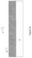
- FIGS. 1 a - care side views detailing an exemplary generation of a solar cell.
- FIGS. 2 a - bdetail the method being applied to a layer disposed upon another layer within a solar cell.
- FIGS. 3 a - bdetail the method being applied to multiple layers disposed upon a rigid substrate within a solar cell.
- Embodiments of the present inventionare described herein in the context of a system and method for creating electric isolation between layers comprising solar cells. Those of ordinary skill in the art will realize that the following detailed description of the present invention is illustrative only and is not intended to be in any way limiting. Other embodiments of the present invention will readily suggest themselves to such skilled persons having the benefit of this disclosure. Reference will now be made in detail to implementations of the present invention as illustrated in the accompanying drawings. The same reference indicators will be used throughout the drawings and the following detailed description to refer to the same or like parts.
- FIGS. 1 a - care side views detailing an exemplary generation of a solar cell.
- FIG. 1 ais a side view of a solar cell showing the preliminary composition of a generic solar cell.
- a solar cell 10has a rigid substrate 12 , upon which a layer of material 14 has been placed. This layer 14 can be placed on the rigid substrate 12 using various means of manufacture, including many semiconductor fabrication techniques. Layer 14 can be of various thicknesses, depending upon the manner in which the layer has been placed upon the rigid substrate.
- layer 14is typically a conductive layer in a solar cell, which serves as one electrode in the makeup of the solar cell.
- layer 14can be a conductive layer, an intrinsic layer, a semiconductor layer, or any other type of layer that could be formed on a rigid substrate using semiconductor manufacturing methods.
- Rigid substrate 12 in this exampleis glass, but again this is demonstrative in nature.
- rigid substrate 12can be any material that is used, or will be used in the future, as a rigid substrate in a semiconductor manufacturing process.
- a first passhas been made with a laser beam over an area of layer 14 .
- the laser beamcan be applied to the top layer, which will cause the material in layer 14 to be rejected from the main mass of solar cell 10 .
- the energy imparted to layer 14can cause the material in the layer 14 to boil, vaporize, or explode away from the main mass of solar cell 10 .
- This expulsion of material from layer 14forms a groove or trench 16 in layer 14 .
- this removal of materialalso results in an electrical isolation between portions of the material, in this diagram portions 14 a and 14 b , respectively.
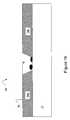
- the cut in the materialmay not prove to be effective to produce as good an electrical isolation as needed between portions 14 a and 14 b .
- portions of the materialmay absorb the energy of the laser beam in the first pass and liquefy without vaporizing.
- the molten materialmay reform at the bottom of the trench 16 .
- molten material from the sides of the layer 14may flow into the trench 16 .
- the laser passmay involve multiple pulses at differing points on the solar cell 10 . In this case, the pulses could produce crater-like results in layer 14 , which effectively act as a first rough electrical isolation step between portions 14 a and 14 b.
- the first laser passcan be applied from the underside of rigid substrate 12 .
- layer 14melts and forms a pool of molten material underneath the top surface of material 14 .
- molten material 14explodes through the surface of layer 14 . In this case, both solid and molten ejecta could fall back into the now-cleaved trench.
- the first laser beam passproduces trench 16 , but remnants of layer 14 may pollute the trench 16 created in the material. Or, the laser process could be somewhat incomplete, again leaving remnants of material 14 in trench 16 . These remnants of material 14 could create electrical pathways through the trench 16 , thus resulting in a lower overall electrical resistance or higher conductance through the trench 14 .
- a second laser beam passhas been made.
- the second laser beam passhas removed a portion of the detritus and ejecta produced by the first laser beam pass.
- the remains of the first laser beam passare removed by the laser beam pass, thus increasing the level of electrical isolation between portions 14 a and 14 b.
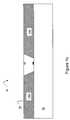
- FIGS. 2 a - bdetail the method being applied to a layer disposed upon another layer within a solar cell. As can be gleaned, embodiments could be applied to more than one layer, or a layer sitting on top of another layer as well.
- FIGS. 2 a - bshow a trench on a topmost layer 24 on a solar cell 20 after being cut through by a first laser beam pass and after a subsequent laser beam pass. The cutting process can either leave remnants of the topmost layer 24 , remnants of the relatively untouched bottom layer 22 , or both, within trench 26 . This is shown in FIG. 2 a . In FIG. 2 b , a second laser beam pass has removed a portion of the remnants, thus increasing the electrical isolation between portions 24 a and 24 b.
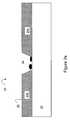
- FIGS. 3 a - bdetail the method being applied to multiple layers disposed upon a rigid substrate within a solar cell.
- a trenchcan be cut through a first layer 34 and a second layer 32 on a solar cell 30 .
- the cutting processcan either leave remnants of the topmost layer 34 , remnants of bottom layer 32 , or both, within the trench 36 .
- FIG. 3 aa second laser beam pass has removed a portion of the remnants, thus increasing the electrical isolation between portions 34 a and 34 b , and/or portions 32 a and 32 b of layer 34 .
- the laser used in the first laser beam pass or the second laser beam passcan be of any variety used to created isolative trenches in semiconductor materials, and can be of the pulse-variety as well.
- the second passmay be carried out by the same laser that was applied with the first path at the same or with different energies and/or beam properties.
- the laser used in the second passcan be another laser with completely differing, similar, or identical characteristics to the first laser.
- the energies applied to the materialscan be of any variety used to created isolative trenches in semiconductor materials.
- the number of subsequent passescan be of any number, although only one is detailed in this application. Further, any of the first pass or the subsequent passes can be made from the top or the bottom of the mass of material.
- the substrate on which the one or more layers to be patternedis rigid.
- Rigidity of a materialcan be measured using several different metrics including, but not limited to, Young's modulus.
- Young's Modulus(also known as the Young Modulus, modulus of elasticity, elastic modulus or tensile modulus) is a measure of the stiffness of a given material. It is defined as the ratio, for small strains, of the rate of change of stress with strain. This can be experimentally determined from the slope of a stress-strain curve created during tensile tests conducted on a sample of the material. Young's modulus for various materials is given in the following table.
- a materiale.g., a substrate
- a materialis deemed to be rigid when it is made of a material that has a Young's modulus of 20 GPa or greater, 30 GPa or greater, 40 GPa or greater, 50 GPa or greater, 60 GPa or greater, or 70 GPa or greater.
- a materiale.g., the substrate
- the substrateis made out of a linear material that obeys Hooke's law. Examples of linear materials include, but are not limited to, steel, carbon fiber, and glass. Rubber and soil (except at very low strains) are non-linear materials.
- the present applicationis not limited to substrates that have rigid cylindrical shapes or are solid rods, or are flat planar. All or a portion of the substrate can be characterized by a cross-section bounded by any one of a number of shapes other than circular.
- the bounding shapecan be any one of circular, ovoid, or any shape characterized by one or more smooth curved surfaces, or any splice of smooth curved surfaces.
- the bounding shapecan be an n-gon, where n is 3, 5, or greater than 5.
- the bounding shapecan also be linear in nature, including triangular, rectangular, pentangular, hexagonal, or having any number of linear segmented surfaces.
- the cross-sectioncan be bounded by any combination of linear surfaces, arcuate surfaces, or curved surfaces.
- an omnifacial circular cross-sectionis illustrated to represent nonplanar embodiments of the photovoltaic device.
- any cross-sectional geometrymay be used in a photovoltaic device 10 that is nonplanar in practice.
- a first portion of the substrateis characterized by a first cross-sectional shape and a second portion of the substrate is characterized by a second cross-sectional shape, where the first and second cross-sectional shapes are the same or different.
- at least ten percent, at least twenty percent, at least thirty percent, at least forty percent, at least fifty percent, at least sixty percent, at least seventy percent, at least eighty percent, at least ninety percent or all of the length of the substrate 102is characterized by the first cross-sectional shape.
- the first cross-sectional shapeis planar (e.g., has no arcuate side) and the second cross-sectional shape has at least one arcuate side.
- the substrateis made of a rigid plastic, metal, metal alloy, or glass.
- the substrateis made of a urethane polymer, an acrylic polymer, a fluoropolymer, polybenzamidazole, polymide, polytetrafluoroethylene, polyetheretherketone, polyamide-imide, glass-based phenolic, polystyrene, cross-linked polystyrene, polyester, polycarbonate, polyethylene, polyethylene, acrylonitrile-butadiene-styrene, polytetrafluoro-ethylene, polymethacrylate, nylon 6,6, cellulose acetate butyrate, cellulose acetate, rigid vinyl, plasticized vinyl, or polypropylene.
- the substrate 102is made of aluminosilicate glass, borosilicate glass, dichroic glass, germanium/semiconductor glass, glass ceramic, silicate/fused silica glass, soda lime glass, quartz glass, chalcogenide/sulphide glass, fluoride glass, a glass-based phenolic, flint glass, or cereated glass.
- the substrateis made of a material such as polybenzamidazole (e.g., CELAZOLE®, available from Boedeker Plastics, Inc., Shiner, Tex.).
- the substrate 102is made of polymide (e.g., DUPONTTM VESPEL®, or DUPONTTM KAPTON®, Wilmington, Del.).
- the substrateis made of polytetrafluoroethylene (PTFE) or polyetheretherketone (PEEK), each of which is available from Boedeker Plastics, Inc.
- the substrateis made of polyamide-imide (e.g., TORLON® PAI, Solvay Advanced Polymers, Alpharetta, Ga.).
- the substrateis made of a glass-based phenolic.
- Phenolic laminatesare made by applying heat and pressure to layers of paper, canvas, linen or glass cloth impregnated with synthetic thermosetting resins. When heat and pressure are applied to the layers, a chemical reaction (polymerization) transforms the separate layers into a single laminated material with a “set” shape that cannot be softened again. Therefore, these materials are called “thermosets.”
- thermosetsA variety of resin types and cloth materials can be used to manufacture thermoset laminates with a range of mechanical, thermal, and electrical properties.
- the substrate 102is a phenoloic laminate having a NEMA grade of G-3, G-5, G-7, G-9, G-10 or G-11. Exemplary phenolic laminates are available from Boedeker Plastics, Inc.
- the substrateis made of polystyrene.
- polystyreneexamples include general purpose polystyrene and high impact polystyrene as detailed in Marks' Standard Handbook for Mechanical Engineers , ninth edition, 1987, McGraw-Hill, Inc., p. 6-174, which is hereby incorporated by reference herein in its entirety.
- the substrate 102is made of cross-linked polystyrene.
- cross-linked polystyreneis REXOLITE® (available from San Diego Plastics Inc., National City, Calif.).
- REXOLITEis a thermoset, in particular a rigid and translucent plastic produced by cross linking polystyrene with divinylbenzene.
- the substrateis made of polycarbonate.
- polycarbonatescan have varying amounts of glass fibers (e.g., 10%, 20%, 30%, or 40%) in order to adjust tensile strength, stiffness, compressive strength, as well as the thermal expansion coefficient of the material.
- Exemplary polycarbonatesare ZELUX® M and ZELUX® W, which are available from Boedeker Plastics, Inc.
- the substrateis made of polyethylene.
- the substrateis made of low density polyethylene (LDPE), high density polyethylene (HDPE), or ultra high molecular weight polyethylene (UHMW PE). Chemical properties of HDPE are described in Marks' Standard Handbook for Mechanical Engineers , ninth edition, 1987, McGraw-Hill, Inc., p. 6-173, which is hereby incorporated by reference herein in its entirety.
- LDPElow density polyethylene
- HDPEhigh density polyethylene
- UHMW PEultra high molecular weight polyethylene
- the substrateis made of acrylonitrile-butadiene-styrene, polytetrafluoro-ethylene (Teflon), polymethacrylate (lucite or plexiglass), nylon 6,6, cellulose acetate butyrate, cellulose acetate, rigid vinyl, plasticized vinyl, or polypropylene. Chemical properties of these materials are described in Marks' Standard Handbook for Mechanical Engineers , ninth edition, 1987, McGraw-Hill, Inc., pp. 6-172 through 6-175, which is hereby incorporated by reference in its entirety.
- a cross-section of the substrateis circumferential and has an outer diameter of between 3 mm and 100 mm, between 4 mm and 75 mm, between 5 mm and 50 mm, between 10 mm and 40 mm, or between 14 mm and 17 mm. In some embodiments, a cross-section of the substrate is circumferential and has an outer diameter of between 1 mm and 1000 mm.
- the substrateis a tube with a hollowed inner portion.
- a cross-section of the substrateis characterized by an inner radius defining the hollowed interior and an outer radius.
- the difference between the inner radius and the outer radiusis the thickness of the substrate.
- the thickness of the substrateis between 0.1 mm and 20 mm, between 0.3 mm and 10 mm, between 0.5 mm and 5 mm, or between 1 mm and 2 mm.
- the inner radiusis between 1 mm and 100 mm, between 3 mm and 50 mm, or between 5 mm and 10 mm.
- the substratehas a length that is between 5 mm and 10,000 mm, between 50 mm and 5,000 mm, between 100 mm and 3000 mm, or between 500 mm and 1500 mm.
- the substrateis a hollowed tube having an outer diameter of 15 mm and a thickness of 1.2 mm, and a length of 1040 mm.
- the substrateis a solid in some embodiments, it will be appreciated that in many embodiments, the substrate will have a hollow core and will adopt a rigid tubular structure such as that formed by a glass tube.
- One aspect of the present applicationprovides a method for forming a patterned layer from common layer in a photovoltaic application, wherein the patterned layer is configured to form one or more portions of one or more solar cells on a rigid substrate.
- common layer 14is patterned to form portions 14 a and 14 b .
- Portions 14 a and 14 bare configured to form one or more portions of one or more solar cells.
- portions 14 a and 14 bcould respectively be the back-electrode of a first and second solar cell that is monolithically integrated onto substrate 12 .
- FIG. 1Ccommon layer 14 is patterned to form portions 14 a and 14 b .
- portions 24 a and 24 bcould respectively be the semiconductor junction of a first and second solar cell that is monolithically integrated onto a substrate that is not shown.
- portions 24 a and 24 bcould respectively be the transparent conducting layer (e.g., transparent conducting oxide) of a first and second solar cell that is monolithically integrated onto a substrate that is not shown.
- a first pass with a first laser beamis made over an area on the common layer.
- a second passis made with a second laser beam over approximately the same area on the common layer.
- the first passprovides a first level of electrical isolation between a first portion and a second portion of the common layer.
- the second passprovides a second level of electrical isolation between the first portion and the second portion of the common layer, the second level of electrical isolation being greater than the first level of electrical isolation.
- the second passcomprises a plurality of laser beam passes.
- the first laser beam and the second laser beamare generated by a common laser apparatus.
- the first laser beam and the second laser beamare each generated by a different laser apparatus.
- the first laser beam or the second laser beamis generated by a pulsed laser.
- the pulsed laserhas a pulse frequency in the range of 0.1 kilohertz (kHz) to 1,000 kHz during a portion of the first pass or a portion of the second pass.
- a dose of radiant energy in a range from 0.01 Joules per square centimeters (J/cm 2 ) to 50.0 j/cm 2is delivered during a portion of the first pass or a portion of the second pass.
- the common layeris a conductive layer.
- the conductive layercomprises aluminum, molybdenum, tungsten, vanadium, rhodium, niobium, chromium, tantalum, titanium, steel, nickel, platinum, silver, gold, an alloy thereof, or any combination thereof.
- the conductive layercomprises indium tin oxide, titanium nitride, tin oxide, fluorine doped tin oxide, doped zinc oxide, aluminum doped zinc oxide, gallium doped zinc oxide, boron dope zinc oxide indium-zinc oxide, a metal-carbon black-filled oxide, a graphite-carbon black-filled oxide, a carbon black-carbon black-filled oxide, a superconductive carbon black-filled oxide, an epoxy, a conductive glass, or a conductive plastic.
Landscapes
- Photovoltaic Devices (AREA)
Abstract
Description
| Young's | ||
| modulus | Young's modulus (E) | |
| Material | (E) in GPa | in lbf/in2(psi) |
| Rubber (small strain) | 0.01-0.1 | 1,500-15,000 |
| Low density polyethylene | 0.2 | 30,000 |
| Polypropylene | 1.5-2 | 217,000-290,000 |
| Polyethylene terephthalate | 2-2.5 | 290,000-360,000 |
| Polystyrene | 3-3.5 | 435,000-505,000 |
| Nylon | 3-7 | 290,000-580,000 |
| Aluminum alloy | 69 | 10,000,000 |
| Glass (all types) | 72 | 10,400,000 |
| Brass and bronze | 103-124 | 17,000,000 |
| Titanium (Ti) | 105-120 | 15,000,000-17,500,000 |
| Carbon fiber reinforced plastic | 150 | 21,800,000 |
| (unidirectional, along grain) | ||
| Wrought iron and steel | 190-210 | 30,000,000 |
| Tungsten (W) | 400-410 | 58,000,000-59,500,000 |
| Silicon carbide (SiC) | 450 | 65,000,000 |
| Tungsten carbide (WC) | 450-650 | 65,000,000-94,000,000 |
| Single Carbon nanotube | 1,000+ | 145,000,000 |
| Diamond (C) | 1,050-1,200 | 150,000,000-175,000,000 |
Claims (48)
Priority Applications (2)
| Application Number | Priority Date | Filing Date | Title |
|---|---|---|---|
| US11/881,000US7879685B2 (en) | 2006-08-04 | 2007-07-25 | System and method for creating electric isolation between layers comprising solar cells |
| US12/885,532US20110318862A1 (en) | 2006-08-04 | 2010-09-19 | System and method for creating electric isolation between layers comprising solar cells |
Applications Claiming Priority (3)
| Application Number | Priority Date | Filing Date | Title |
|---|---|---|---|
| US83572406P | 2006-08-04 | 2006-08-04 | |
| US11/499,608US20080029152A1 (en) | 2006-08-04 | 2006-08-04 | Laser scribing apparatus, systems, and methods |
| US11/881,000US7879685B2 (en) | 2006-08-04 | 2007-07-25 | System and method for creating electric isolation between layers comprising solar cells |
Related Parent Applications (1)
| Application Number | Title | Priority Date | Filing Date |
|---|---|---|---|
| US11/499,608Continuation-In-PartUS20080029152A1 (en) | 2006-08-04 | 2006-08-04 | Laser scribing apparatus, systems, and methods |
Related Child Applications (1)
| Application Number | Title | Priority Date | Filing Date |
|---|---|---|---|
| US12/885,532ContinuationUS20110318862A1 (en) | 2006-08-04 | 2010-09-19 | System and method for creating electric isolation between layers comprising solar cells |
Publications (2)
| Publication Number | Publication Date |
|---|---|
| US20080029154A1 US20080029154A1 (en) | 2008-02-07 |
| US7879685B2true US7879685B2 (en) | 2011-02-01 |
Family
ID=38728892
Family Applications (2)
| Application Number | Title | Priority Date | Filing Date |
|---|---|---|---|
| US11/881,000Expired - Fee RelatedUS7879685B2 (en) | 2006-08-04 | 2007-07-25 | System and method for creating electric isolation between layers comprising solar cells |
| US12/885,532AbandonedUS20110318862A1 (en) | 2006-08-04 | 2010-09-19 | System and method for creating electric isolation between layers comprising solar cells |
Family Applications After (1)
| Application Number | Title | Priority Date | Filing Date |
|---|---|---|---|
| US12/885,532AbandonedUS20110318862A1 (en) | 2006-08-04 | 2010-09-19 | System and method for creating electric isolation between layers comprising solar cells |
Country Status (2)
| Country | Link |
|---|---|
| US (2) | US7879685B2 (en) |
| WO (1) | WO2008019073A2 (en) |
Cited By (1)
| Publication number | Priority date | Publication date | Assignee | Title |
|---|---|---|---|---|
| US20110209746A1 (en)* | 2009-09-06 | 2011-09-01 | Hanzhong Zhang | Tubular Photovoltaic Device and Method of Making |
Families Citing this family (41)
| Publication number | Priority date | Publication date | Assignee | Title |
|---|---|---|---|---|
| US9105776B2 (en)* | 2006-05-15 | 2015-08-11 | Stion Corporation | Method and structure for thin film photovoltaic materials using semiconductor materials |
| US8017860B2 (en) | 2006-05-15 | 2011-09-13 | Stion Corporation | Method and structure for thin film photovoltaic materials using bulk semiconductor materials |
| WO2008157807A2 (en)* | 2007-06-20 | 2008-12-24 | Ascent Solar Technologies, Inc. | Array of monolithically integrated thin film photovoltaic cells and associated methods |
| US8071179B2 (en) | 2007-06-29 | 2011-12-06 | Stion Corporation | Methods for infusing one or more materials into nano-voids if nanoporous or nanostructured materials |
| US8759671B2 (en)* | 2007-09-28 | 2014-06-24 | Stion Corporation | Thin film metal oxide bearing semiconductor material for single junction solar cell devices |
| US7998762B1 (en) | 2007-11-14 | 2011-08-16 | Stion Corporation | Method and system for large scale manufacture of thin film photovoltaic devices using multi-chamber configuration |
| US8772078B1 (en) | 2008-03-03 | 2014-07-08 | Stion Corporation | Method and system for laser separation for exclusion region of multi-junction photovoltaic materials |
| WO2009124180A2 (en)* | 2008-04-02 | 2009-10-08 | The Trustees Of Columbia University In The City Of New York | In situ plating and soldering of materials covered with a surface film |
| US8642138B2 (en) | 2008-06-11 | 2014-02-04 | Stion Corporation | Processing method for cleaning sulfur entities of contact regions |
| US12074240B2 (en)* | 2008-06-12 | 2024-08-27 | Maxeon Solar Pte. Ltd. | Backside contact solar cells with separated polysilicon doped regions |
| US7851698B2 (en)* | 2008-06-12 | 2010-12-14 | Sunpower Corporation | Trench process and structure for backside contact solar cells with polysilicon doped regions |
| US8003432B2 (en) | 2008-06-25 | 2011-08-23 | Stion Corporation | Consumable adhesive layer for thin film photovoltaic material |
| US9087943B2 (en)* | 2008-06-25 | 2015-07-21 | Stion Corporation | High efficiency photovoltaic cell and manufacturing method free of metal disulfide barrier material |
| US20100323471A1 (en)* | 2008-08-21 | 2010-12-23 | Applied Materials, Inc. | Selective Etch of Laser Scribed Solar Cell Substrate |
| US7855089B2 (en)* | 2008-09-10 | 2010-12-21 | Stion Corporation | Application specific solar cell and method for manufacture using thin film photovoltaic materials |
| US8383450B2 (en)* | 2008-09-30 | 2013-02-26 | Stion Corporation | Large scale chemical bath system and method for cadmium sulfide processing of thin film photovoltaic materials |
| US7910399B1 (en) | 2008-09-30 | 2011-03-22 | Stion Corporation | Thermal management and method for large scale processing of CIS and/or CIGS based thin films overlying glass substrates |
| US7863074B2 (en)* | 2008-09-30 | 2011-01-04 | Stion Corporation | Patterning electrode materials free from berm structures for thin film photovoltaic cells |
| US7947524B2 (en)* | 2008-09-30 | 2011-05-24 | Stion Corporation | Humidity control and method for thin film photovoltaic materials |
| US8425739B1 (en) | 2008-09-30 | 2013-04-23 | Stion Corporation | In chamber sodium doping process and system for large scale cigs based thin film photovoltaic materials |
| US8741689B2 (en)* | 2008-10-01 | 2014-06-03 | Stion Corporation | Thermal pre-treatment process for soda lime glass substrate for thin film photovoltaic materials |
| US20110018103A1 (en) | 2008-10-02 | 2011-01-27 | Stion Corporation | System and method for transferring substrates in large scale processing of cigs and/or cis devices |
| US8168463B2 (en) | 2008-10-17 | 2012-05-01 | Stion Corporation | Zinc oxide film method and structure for CIGS cell |
| US8344243B2 (en)* | 2008-11-20 | 2013-01-01 | Stion Corporation | Method and structure for thin film photovoltaic cell using similar material junction |
| KR100993343B1 (en) | 2009-01-06 | 2010-11-10 | 주식회사 엘티에스 | Electrode pattern forming device of solar cell |
| US8372684B1 (en) | 2009-05-14 | 2013-02-12 | Stion Corporation | Method and system for selenization in fabricating CIGS/CIS solar cells |
| JP5473414B2 (en)* | 2009-06-10 | 2014-04-16 | 株式会社ディスコ | Laser processing equipment |
| US8507786B1 (en) | 2009-06-27 | 2013-08-13 | Stion Corporation | Manufacturing method for patterning CIGS/CIS solar cells |
| US8398772B1 (en) | 2009-08-18 | 2013-03-19 | Stion Corporation | Method and structure for processing thin film PV cells with improved temperature uniformity |
| US8809096B1 (en) | 2009-10-22 | 2014-08-19 | Stion Corporation | Bell jar extraction tool method and apparatus for thin film photovoltaic materials |
| US8859880B2 (en) | 2010-01-22 | 2014-10-14 | Stion Corporation | Method and structure for tiling industrial thin-film solar devices |
| US8263494B2 (en) | 2010-01-25 | 2012-09-11 | Stion Corporation | Method for improved patterning accuracy for thin film photovoltaic panels |
| US9096930B2 (en) | 2010-03-29 | 2015-08-04 | Stion Corporation | Apparatus for manufacturing thin film photovoltaic devices |
| US8461061B2 (en) | 2010-07-23 | 2013-06-11 | Stion Corporation | Quartz boat method and apparatus for thin film thermal treatment |
| US8628997B2 (en) | 2010-10-01 | 2014-01-14 | Stion Corporation | Method and device for cadmium-free solar cells |
| US8728200B1 (en) | 2011-01-14 | 2014-05-20 | Stion Corporation | Method and system for recycling processing gas for selenization of thin film photovoltaic materials |
| US8998606B2 (en) | 2011-01-14 | 2015-04-07 | Stion Corporation | Apparatus and method utilizing forced convection for uniform thermal treatment of thin film devices |
| US8436445B2 (en) | 2011-08-15 | 2013-05-07 | Stion Corporation | Method of manufacture of sodium doped CIGS/CIGSS absorber layers for high efficiency photovoltaic devices |
| CN108604611A (en)* | 2015-12-10 | 2018-09-28 | 松下知识产权经营株式会社 | Solar cell module |
| JP6666173B2 (en)* | 2016-03-09 | 2020-03-13 | 株式会社ディスコ | Laser processing equipment |
| JP7278831B2 (en)* | 2019-03-27 | 2023-05-22 | パナソニックホールディングス株式会社 | SOLAR BATTERY CELL MANUFACTURING METHOD AND CUTTING SOLAR BATTERY CELL |
Citations (68)
| Publication number | Priority date | Publication date | Assignee | Title |
|---|---|---|---|---|
| US2984775A (en) | 1958-07-09 | 1961-05-16 | Hoffman Electronics Corp | Ruggedized solar cell and process for making the same or the like |
| US3005862A (en) | 1958-09-15 | 1961-10-24 | Int Rectifier Corp | Solar battery mounting means |
| US3046324A (en) | 1961-01-16 | 1962-07-24 | Hoffman Electronics Corp | Alloyed photovoltaic cell and method of making the same |
| US3976508A (en) | 1974-11-01 | 1976-08-24 | Mobil Tyco Solar Energy Corporation | Tubular solar cell devices |
| US3990914A (en) | 1974-09-03 | 1976-11-09 | Sensor Technology, Inc. | Tubular solar cell |
| FR2327643A1 (en) | 1975-10-09 | 1977-05-06 | Commissariat Energie Atomique | LUMINOUS ENERGY INTO ELECTRICAL ENERGY CONVERTER |
| US4113531A (en) | 1976-10-26 | 1978-09-12 | Hughes Aircraft Company | Process for fabricating polycrystalline inp-cds solar cells |
| US4292093A (en)* | 1979-12-28 | 1981-09-29 | The United States Of America As Represented By The United States Department Of Energy | Method using laser irradiation for the production of atomically clean crystalline silicon and germanium surfaces |
| US4292092A (en) | 1980-06-02 | 1981-09-29 | Rca Corporation | Laser processing technique for fabricating series-connected and tandem junction series-connected solar cells into a solar battery |
| DE3209548A1 (en) | 1982-03-16 | 1983-10-20 | Siemens AG, 1000 Berlin und 8000 München | Solar cell arrangement in thin-layer construction made from semiconductor material, and process for the fabrication thereof |
| JPS59125670A (en) | 1983-01-06 | 1984-07-20 | Toppan Printing Co Ltd | solar cells |
| JPS59143377A (en) | 1983-02-05 | 1984-08-16 | Toyobo Co Ltd | Thread type solar battery |
| JPS59144177A (en) | 1983-02-07 | 1984-08-18 | Seiko Epson Corp | Solar battery |
| WO1984004425A1 (en) | 1983-04-25 | 1984-11-08 | Inst Microtechnique De L Unive | Large surface photovoltaic cell and production method thereof |
| US4497974A (en) | 1982-11-22 | 1985-02-05 | Exxon Research & Engineering Co. | Realization of a thin film solar cell with a detached reflector |
| US4686323A (en) | 1986-06-30 | 1987-08-11 | The Standard Oil Company | Multiple cell, two terminal photovoltaic device employing conductively adhered cells |
| US4726849A (en) | 1985-08-07 | 1988-02-23 | Sanyo Electric Co., Ltd | Photovoltaic device and a method of manufacturing thereof |
| US4728615A (en) | 1984-10-17 | 1988-03-01 | Fuji Electric Company Ltd. | Method for producing thin-film photoelectric transducer |
| DE3801989A1 (en) | 1988-01-23 | 1989-07-27 | Licentia Gmbh | INSULATED GLASS PANEL |
| US4913744A (en) | 1987-01-13 | 1990-04-03 | Helmut Hoegl | Solar cell arrangement |
| EP0427934A2 (en) | 1989-09-08 | 1991-05-22 | Solarex Corporation | Monolithic module comprising series and parallel connected photovoltaic cells |
| US5093279A (en) | 1991-02-01 | 1992-03-03 | International Business Machines Corporation | Laser ablation damascene process |
| EP0575848A2 (en) | 1992-06-22 | 1993-12-29 | Martin Marietta Corporation | Ablative process for printed circuit board technology |
| DE4339547A1 (en) | 1993-11-19 | 1995-05-24 | Twin Solar Technik Entwicklung | Photovoltaic electricity generation by solar cells |
| DE4343514A1 (en) | 1993-12-20 | 1995-06-22 | Peter Pelz | Roof or wall element fitted with solar module |
| US5437736A (en) | 1994-02-15 | 1995-08-01 | Cole; Eric D. | Semiconductor fiber solar cells and modules |
| DE4406760A1 (en) | 1994-03-02 | 1995-09-07 | Twin Solar Technik Entwicklung | Transparent photovoltaic solar cell module |
| WO1996009128A1 (en) | 1994-09-19 | 1996-03-28 | Cauldron Limited Partnership | Selective removal of material by irradiation |
| US5735966A (en) | 1995-05-15 | 1998-04-07 | Luch; Daniel | Substrate structures for integrated series connected photovoltaic arrays and process of manufacture of such arrays |
| US5780805A (en) | 1995-05-03 | 1998-07-14 | Gerber Garment Technology, Inc. | Pattern shifting laser cutter |
| US5841099A (en) | 1994-07-18 | 1998-11-24 | Electro Scientific Industries, Inc. | Method employing UV laser pulses of varied energy density to form depthwise self-limiting blind vias in multilayered targets |
| DE19732876A1 (en) | 1997-07-30 | 1999-02-04 | Reitstall Icking Gmbh | Photovoltaic solar energy module |
| US5902416A (en) | 1993-08-27 | 1999-05-11 | Twin Solar-Technik Entwicklungs-Gmbh | Element of a photovoltaic solar cell and a process for the production thereof as well as the arrangement thereof in a solar cell |
| US5958268A (en) | 1995-06-07 | 1999-09-28 | Cauldron Limited Partnership | Removal of material by polarized radiation |
| US6018123A (en) | 1996-01-31 | 2000-01-25 | Canon Kabushiki Kaisha | Heat collector with solar cell and passive solar apparatus |
| US6066830A (en)* | 1998-06-04 | 2000-05-23 | Astronics Corporation | Laser etching of electroluminescent lamp electrode structures, and electroluminescent lamps produced thereby |
| US6107564A (en) | 1997-11-18 | 2000-08-22 | Deposition Sciences, Inc. | Solar cell cover and coating |
| EP1029959A1 (en) | 1999-01-22 | 2000-08-23 | Griffith Textile Machines Limited | A tuft yarn selection mechanism |
| WO2000060655A1 (en) | 1999-04-05 | 2000-10-12 | Ultratech Stepper, Inc. | Methods for determining wavelength and pulse length of radiant energy used for annealing |
| DE19933703A1 (en) | 1999-04-07 | 2000-10-19 | Siemens Solar Gmbh | Device and method for removing layers on a workpiece |
| US6258620B1 (en) | 1997-10-15 | 2001-07-10 | University Of South Florida | Method of manufacturing CIGS photovoltaic devices |
| US6294723B2 (en) | 1998-02-26 | 2001-09-25 | Hitachi, Ltd. | Photovoltaic device, photovoltaic module and establishing method of photovoltaic system |
| US6355873B1 (en) | 2000-06-21 | 2002-03-12 | Ball Semiconductor, Inc. | Spherical shaped solar cell fabrication and panel assembly |
| US6359210B2 (en) | 1998-05-28 | 2002-03-19 | Tecstar Power System, Inc. | Solar cell having an integral monolithically grown bypass diode |
| US6410843B1 (en) | 1999-11-22 | 2002-06-25 | Sanyo Electric Co., Ltd. | Solar cell module |
| US20020130311A1 (en) | 2000-08-22 | 2002-09-19 | Lieber Charles M. | Doped elongated semiconductors, growing such semiconductors, devices including such semiconductors and fabricating such devices |
| WO2002078896A1 (en) | 2001-03-29 | 2002-10-10 | Gsi Lumonics Corporation | Methods and systems for processing a device, methods and systems for modeling same and the device |
| US20020180909A1 (en) | 2001-03-26 | 2002-12-05 | Lubart Neil D. | Device having reflective and transmissive properties |
| US6541695B1 (en) | 1992-09-21 | 2003-04-01 | Thomas Mowles | High efficiency solar photovoltaic cells produced with inexpensive materials by processes suitable for large volume production |
| US6544865B1 (en)* | 1998-04-09 | 2003-04-08 | Pacific Solar Pty. Limited | Metal film interrupting process |
| US20030068559A1 (en) | 2001-09-12 | 2003-04-10 | Armstrong Joseph H. | Apparatus and method for the design and manufacture of multifunctional composite materials with power integration |
| US6548751B2 (en) | 2000-12-12 | 2003-04-15 | Solarflex Technologies, Inc. | Thin film flexible solar cell |
| US6555739B2 (en) | 2001-09-10 | 2003-04-29 | Ekla-Tek, Llc | Photovoltaic array and method of manufacturing same |
| WO2003061013A1 (en) | 2002-01-07 | 2003-07-24 | Bp Corporation North America Inc. | Method of manufacturing thin film photovoltaic modules |
| US20030155003A1 (en) | 2002-01-07 | 2003-08-21 | Alcatel | Solar energy concentrator device for spacecraft and a solar generator panel |
| US20030180983A1 (en) | 2002-01-07 | 2003-09-25 | Oswald Robert S. | Method of manufacturing thin film photovoltaic modules |
| US6706959B2 (en) | 2000-11-24 | 2004-03-16 | Clean Venture 21 Corporation | Photovoltaic apparatus and mass-producing apparatus for mass-producing spherical semiconductor particles |
| US6706963B2 (en) | 2002-01-25 | 2004-03-16 | Konarka Technologies, Inc. | Photovoltaic cell interconnection |
| US20040063320A1 (en) | 2002-09-30 | 2004-04-01 | Hollars Dennis R. | Manufacturing apparatus and method for large-scale production of thin-film solar cells |
| US6762359B2 (en) | 2001-01-15 | 2004-07-13 | Fuji Machine Mfg. Co., Ltd. | Photovoltaic panel and method of producing same |
| WO2004061417A2 (en) | 2002-12-26 | 2004-07-22 | Genorx, Inc. | Device structure for closely spaced electrodes |
| US6806414B2 (en) | 2001-05-09 | 2004-10-19 | Canon Kabushiki Kaisha | Photovoltaic elements |
| DE10326505A1 (en) | 2003-06-10 | 2005-01-13 | Solarion Gmbh | Process for removing material in the structuring of a thin layer semiconductor component used for photovoltaic cells comprises directing laser beam having selected pulse duration and wavelength on the layer side of the component |
| WO2005034149A2 (en) | 2003-10-02 | 2005-04-14 | Scheuten Glasgroep | Spherical or grain-shaped semiconductor element for use in solar cells and method for producing the same; method for producing a solar cell comprising said semiconductor element and solar cell |
| US6888987B2 (en) | 2000-02-17 | 2005-05-03 | Xponent Photonics Inc | Cylindrical processing of optical media |
| US20050098202A1 (en) | 2003-11-10 | 2005-05-12 | Maltby Robert E.Jr. | Non-planar photocell |
| US20050271796A1 (en) | 2001-09-12 | 2005-12-08 | Neudecker Bernd J | Thin-film electrochemical devices on fibrous or ribbon-like substrates and method for their manufacture and design |
| US7235736B1 (en) | 2006-03-18 | 2007-06-26 | Solyndra, Inc. | Monolithic integration of cylindrical solar cells |
Family Cites Families (7)
| Publication number | Priority date | Publication date | Assignee | Title |
|---|---|---|---|---|
| US180983A (en)* | 1876-08-15 | Improvement in fire-alarm-telegraph circuits | ||
| US4144095A (en)* | 1975-09-08 | 1979-03-13 | Mobil Tyco Solar Energy Corporation | Solar energy assembly |
| US4341918A (en)* | 1980-12-24 | 1982-07-27 | The United States Of America As Represented By The Administrator Of The National Aeronautics And Space Administration | High voltage planar multijunction solar cell |
| JPS63250881A (en)* | 1987-04-07 | 1988-10-18 | Semiconductor Energy Lab Co Ltd | Manufacture of superconductor |
| US4870244A (en)* | 1988-10-07 | 1989-09-26 | Copley John A | Method and device for stand-off laser drilling and cutting |
| US5958526A (en)* | 1998-05-14 | 1999-09-28 | Spickelmire; James | Adhesive camouflage patch |
| US6509546B1 (en)* | 2000-03-15 | 2003-01-21 | International Business Machines Corporation | Laser excision of laminate chip carriers |
- 2007
- 2007-07-25USUS11/881,000patent/US7879685B2/ennot_activeExpired - Fee Related
- 2007-08-03WOPCT/US2007/017357patent/WO2008019073A2/enactiveApplication Filing
- 2010
- 2010-09-19USUS12/885,532patent/US20110318862A1/ennot_activeAbandoned
Patent Citations (69)
| Publication number | Priority date | Publication date | Assignee | Title |
|---|---|---|---|---|
| US2984775A (en) | 1958-07-09 | 1961-05-16 | Hoffman Electronics Corp | Ruggedized solar cell and process for making the same or the like |
| US3005862A (en) | 1958-09-15 | 1961-10-24 | Int Rectifier Corp | Solar battery mounting means |
| US3046324A (en) | 1961-01-16 | 1962-07-24 | Hoffman Electronics Corp | Alloyed photovoltaic cell and method of making the same |
| US3990914A (en) | 1974-09-03 | 1976-11-09 | Sensor Technology, Inc. | Tubular solar cell |
| US3976508A (en) | 1974-11-01 | 1976-08-24 | Mobil Tyco Solar Energy Corporation | Tubular solar cell devices |
| USRE29833E (en) | 1974-11-01 | 1978-11-14 | Mobil Tyco Solar Energy Corporation | Tubular solar cell devices |
| FR2327643A1 (en) | 1975-10-09 | 1977-05-06 | Commissariat Energie Atomique | LUMINOUS ENERGY INTO ELECTRICAL ENERGY CONVERTER |
| US4113531A (en) | 1976-10-26 | 1978-09-12 | Hughes Aircraft Company | Process for fabricating polycrystalline inp-cds solar cells |
| US4292093A (en)* | 1979-12-28 | 1981-09-29 | The United States Of America As Represented By The United States Department Of Energy | Method using laser irradiation for the production of atomically clean crystalline silicon and germanium surfaces |
| US4292092A (en) | 1980-06-02 | 1981-09-29 | Rca Corporation | Laser processing technique for fabricating series-connected and tandem junction series-connected solar cells into a solar battery |
| DE3209548A1 (en) | 1982-03-16 | 1983-10-20 | Siemens AG, 1000 Berlin und 8000 München | Solar cell arrangement in thin-layer construction made from semiconductor material, and process for the fabrication thereof |
| US4497974A (en) | 1982-11-22 | 1985-02-05 | Exxon Research & Engineering Co. | Realization of a thin film solar cell with a detached reflector |
| JPS59125670A (en) | 1983-01-06 | 1984-07-20 | Toppan Printing Co Ltd | solar cells |
| JPS59143377A (en) | 1983-02-05 | 1984-08-16 | Toyobo Co Ltd | Thread type solar battery |
| JPS59144177A (en) | 1983-02-07 | 1984-08-18 | Seiko Epson Corp | Solar battery |
| WO1984004425A1 (en) | 1983-04-25 | 1984-11-08 | Inst Microtechnique De L Unive | Large surface photovoltaic cell and production method thereof |
| US4728615A (en) | 1984-10-17 | 1988-03-01 | Fuji Electric Company Ltd. | Method for producing thin-film photoelectric transducer |
| US4726849A (en) | 1985-08-07 | 1988-02-23 | Sanyo Electric Co., Ltd | Photovoltaic device and a method of manufacturing thereof |
| US4686323A (en) | 1986-06-30 | 1987-08-11 | The Standard Oil Company | Multiple cell, two terminal photovoltaic device employing conductively adhered cells |
| US4913744A (en) | 1987-01-13 | 1990-04-03 | Helmut Hoegl | Solar cell arrangement |
| DE3801989A1 (en) | 1988-01-23 | 1989-07-27 | Licentia Gmbh | INSULATED GLASS PANEL |
| EP0427934A2 (en) | 1989-09-08 | 1991-05-22 | Solarex Corporation | Monolithic module comprising series and parallel connected photovoltaic cells |
| US5093279A (en) | 1991-02-01 | 1992-03-03 | International Business Machines Corporation | Laser ablation damascene process |
| EP0575848A2 (en) | 1992-06-22 | 1993-12-29 | Martin Marietta Corporation | Ablative process for printed circuit board technology |
| US6541695B1 (en) | 1992-09-21 | 2003-04-01 | Thomas Mowles | High efficiency solar photovoltaic cells produced with inexpensive materials by processes suitable for large volume production |
| US5902416A (en) | 1993-08-27 | 1999-05-11 | Twin Solar-Technik Entwicklungs-Gmbh | Element of a photovoltaic solar cell and a process for the production thereof as well as the arrangement thereof in a solar cell |
| DE4339547A1 (en) | 1993-11-19 | 1995-05-24 | Twin Solar Technik Entwicklung | Photovoltaic electricity generation by solar cells |
| DE4343514A1 (en) | 1993-12-20 | 1995-06-22 | Peter Pelz | Roof or wall element fitted with solar module |
| US5437736A (en) | 1994-02-15 | 1995-08-01 | Cole; Eric D. | Semiconductor fiber solar cells and modules |
| DE4406760A1 (en) | 1994-03-02 | 1995-09-07 | Twin Solar Technik Entwicklung | Transparent photovoltaic solar cell module |
| US5841099A (en) | 1994-07-18 | 1998-11-24 | Electro Scientific Industries, Inc. | Method employing UV laser pulses of varied energy density to form depthwise self-limiting blind vias in multilayered targets |
| WO1996009128A1 (en) | 1994-09-19 | 1996-03-28 | Cauldron Limited Partnership | Selective removal of material by irradiation |
| US5780805A (en) | 1995-05-03 | 1998-07-14 | Gerber Garment Technology, Inc. | Pattern shifting laser cutter |
| US5735966A (en) | 1995-05-15 | 1998-04-07 | Luch; Daniel | Substrate structures for integrated series connected photovoltaic arrays and process of manufacture of such arrays |
| US5958268A (en) | 1995-06-07 | 1999-09-28 | Cauldron Limited Partnership | Removal of material by polarized radiation |
| US6018123A (en) | 1996-01-31 | 2000-01-25 | Canon Kabushiki Kaisha | Heat collector with solar cell and passive solar apparatus |
| DE19732876A1 (en) | 1997-07-30 | 1999-02-04 | Reitstall Icking Gmbh | Photovoltaic solar energy module |
| US6258620B1 (en) | 1997-10-15 | 2001-07-10 | University Of South Florida | Method of manufacturing CIGS photovoltaic devices |
| US6107564A (en) | 1997-11-18 | 2000-08-22 | Deposition Sciences, Inc. | Solar cell cover and coating |
| US6294723B2 (en) | 1998-02-26 | 2001-09-25 | Hitachi, Ltd. | Photovoltaic device, photovoltaic module and establishing method of photovoltaic system |
| US6544865B1 (en)* | 1998-04-09 | 2003-04-08 | Pacific Solar Pty. Limited | Metal film interrupting process |
| US6359210B2 (en) | 1998-05-28 | 2002-03-19 | Tecstar Power System, Inc. | Solar cell having an integral monolithically grown bypass diode |
| US6066830A (en)* | 1998-06-04 | 2000-05-23 | Astronics Corporation | Laser etching of electroluminescent lamp electrode structures, and electroluminescent lamps produced thereby |
| EP1029959A1 (en) | 1999-01-22 | 2000-08-23 | Griffith Textile Machines Limited | A tuft yarn selection mechanism |
| WO2000060655A1 (en) | 1999-04-05 | 2000-10-12 | Ultratech Stepper, Inc. | Methods for determining wavelength and pulse length of radiant energy used for annealing |
| DE19933703A1 (en) | 1999-04-07 | 2000-10-19 | Siemens Solar Gmbh | Device and method for removing layers on a workpiece |
| US6410843B1 (en) | 1999-11-22 | 2002-06-25 | Sanyo Electric Co., Ltd. | Solar cell module |
| US6888987B2 (en) | 2000-02-17 | 2005-05-03 | Xponent Photonics Inc | Cylindrical processing of optical media |
| US6355873B1 (en) | 2000-06-21 | 2002-03-12 | Ball Semiconductor, Inc. | Spherical shaped solar cell fabrication and panel assembly |
| US20020130311A1 (en) | 2000-08-22 | 2002-09-19 | Lieber Charles M. | Doped elongated semiconductors, growing such semiconductors, devices including such semiconductors and fabricating such devices |
| US6706959B2 (en) | 2000-11-24 | 2004-03-16 | Clean Venture 21 Corporation | Photovoltaic apparatus and mass-producing apparatus for mass-producing spherical semiconductor particles |
| US6548751B2 (en) | 2000-12-12 | 2003-04-15 | Solarflex Technologies, Inc. | Thin film flexible solar cell |
| US6762359B2 (en) | 2001-01-15 | 2004-07-13 | Fuji Machine Mfg. Co., Ltd. | Photovoltaic panel and method of producing same |
| US20020180909A1 (en) | 2001-03-26 | 2002-12-05 | Lubart Neil D. | Device having reflective and transmissive properties |
| WO2002078896A1 (en) | 2001-03-29 | 2002-10-10 | Gsi Lumonics Corporation | Methods and systems for processing a device, methods and systems for modeling same and the device |
| US6806414B2 (en) | 2001-05-09 | 2004-10-19 | Canon Kabushiki Kaisha | Photovoltaic elements |
| US6555739B2 (en) | 2001-09-10 | 2003-04-29 | Ekla-Tek, Llc | Photovoltaic array and method of manufacturing same |
| US20030068559A1 (en) | 2001-09-12 | 2003-04-10 | Armstrong Joseph H. | Apparatus and method for the design and manufacture of multifunctional composite materials with power integration |
| US20050271796A1 (en) | 2001-09-12 | 2005-12-08 | Neudecker Bernd J | Thin-film electrochemical devices on fibrous or ribbon-like substrates and method for their manufacture and design |
| US20030180983A1 (en) | 2002-01-07 | 2003-09-25 | Oswald Robert S. | Method of manufacturing thin film photovoltaic modules |
| US20030155003A1 (en) | 2002-01-07 | 2003-08-21 | Alcatel | Solar energy concentrator device for spacecraft and a solar generator panel |
| WO2003061013A1 (en) | 2002-01-07 | 2003-07-24 | Bp Corporation North America Inc. | Method of manufacturing thin film photovoltaic modules |
| US6706963B2 (en) | 2002-01-25 | 2004-03-16 | Konarka Technologies, Inc. | Photovoltaic cell interconnection |
| US20040063320A1 (en) | 2002-09-30 | 2004-04-01 | Hollars Dennis R. | Manufacturing apparatus and method for large-scale production of thin-film solar cells |
| WO2004061417A2 (en) | 2002-12-26 | 2004-07-22 | Genorx, Inc. | Device structure for closely spaced electrodes |
| DE10326505A1 (en) | 2003-06-10 | 2005-01-13 | Solarion Gmbh | Process for removing material in the structuring of a thin layer semiconductor component used for photovoltaic cells comprises directing laser beam having selected pulse duration and wavelength on the layer side of the component |
| WO2005034149A2 (en) | 2003-10-02 | 2005-04-14 | Scheuten Glasgroep | Spherical or grain-shaped semiconductor element for use in solar cells and method for producing the same; method for producing a solar cell comprising said semiconductor element and solar cell |
| US20050098202A1 (en) | 2003-11-10 | 2005-05-12 | Maltby Robert E.Jr. | Non-planar photocell |
| US7235736B1 (en) | 2006-03-18 | 2007-06-26 | Solyndra, Inc. | Monolithic integration of cylindrical solar cells |
Non-Patent Citations (46)
| Title |
|---|
| Birkmire et al., 1997, "Polycrystalline Thin Film Solar Cells: Present Status and Future Potential," Annu. Rev. Mater. Sci. 1997 27: 625-653. |
| Birkmire et al., 2005, "Cu(InGa)Se2 Solar Cells on a Flexible Polymer Web," Prog. Photovolt 13: 141-148. |
| Bube, 1998, "Photovoltaic Materials," Properties of Semiconductor Materials 1: 1-277. |
| Chaisitak et al., 2000, "Improvement in Performances of ZnO:B/i-ZnO/Cu(InGa)Se2 Solar Cells by Surface Treatments for Cu(InGa)Se2," The Japan Society of Applied Physics 39: 1660-1664. |
| Collares-Pereira et al., 1989, "Amorphous Silicon Photovoltaic Solar Cells-Inexpensive, High-Yield Optical Designs," ASME 111: 112-116. |
| Compaan et al., 1996, "Pulse Duration and Wavelength Effects in Laser Scribing of Thin-Film Polycrystalline PV Materials," AIP Conference Proceedings of the 14th Conference Lakewood, Colorado, Nov. 1996 364:567-571. |
| Compaan et al., 1998, "Lasers and Beam Delivery Options for Polycrystalline Thin-Film Scribing," AIP Conference Proceedings of the 15th Conference Denver, Colorado, Sep. 1998 462:42-47. |
| Compaan et al., 1998, "Optimization of Laser Scribing for Thin-Film PV Modules," Final Technical Progress Report Apr. 12, 1995-Oct. 11, 1997, National Renewal Energy Laboratory: 38 pages. |
| Compaan et al., 2000, "Laser scribing of polycrystalline thin films," Optics and Lasers in Engineering 34: 15-45. |
| Compaan, 2000, "Laser scribing creates monolithic thin-film arrays," Laser Focus World, www. optoelectronics-world.com Jan. 2000: 147-152. |
| Cuevas et al., 1982, "50 Per Cent More Output Power from an Albedo-collecting Flat Panel Using Bifacial Solar Cells," Solar Energy 29: 419-420. |
| Edmonds, 1990, "The Performance of Bifacial Solar Cells in Static Solar Concentrators," Solar Energy Materials 21: 173-190. |
| Golay et al., "Laser Scribing of p-i-n/p-i-n "Miormorph" (a-Si:H/muc-Si:H) Tandem Cells," Abstract, www-micromorph.unine.ch/publications/PS-files/paper-319.pdf, 2000. |
| Golay et al., "Laser Scribing of p-i-n/p-i-n "Miormorph" (a-Si:H/μc-Si:H) Tandem Cells," Abstract, www-micromorph.unine.ch/publications/PS—files/paper—319.pdf, 2000. |
| International Search Report and Written Opinion dated Feb. 21, 2008 for International Application No. PCT/US2007/017357. |
| Jensen et al., 2003, "Back Contact Cracking During Fabrication of CIGS Solar Cells on Polyimide Substrates," NREL/CD, 877-881. |
| Jiang et al., 2003, Femtosecond Lasers Ablation: Challenges and Opportunities, Department of Mechanical and Aerospace Engineering and Engineering Mechanics, University of Missouri-Rolla, Rolla, Missouri, web.umr.edu/~laser/paper/femtosecond-rev-NSFWorkshop.pdf : 1-15. |
| Jiang et al., 2003, Femtosecond Lasers Ablation: Challenges and Opportunities, Department of Mechanical and Aerospace Engineering and Engineering Mechanics, University of Missouri-Rolla, Rolla, Missouri, web.umr.edu/˜laser/paper/femtosecond—rev—NSFWorkshop.pdf : 1-15. |
| Joliet et al., 1985, "Laser-induced Synthesis of Thin CuInSe-2 Films," Appl. Phys. Lett. 46: 266-267. |
| Khosrofian et al., 1983, "Measurement of a Gaussian Laser Beam Diameter Through the Direct Inversion of Knife-edge Data," Applied Optics 22: 3406-3410. |
| Lambin et al., 1983, "Complete calculation of the electric potential produced by a pair of current source and sink energizing a circular finite-length cylinder," J. Appl. Phys. 54(7): 4174-4184. |
| Lugue et al., 2003, "Handbook of Photovoltaic Science and Engineering," Wiley, 1-662. |
| Lugue, 1984, "Static Concentrators: A Venture to Meet the Low Cost Target in Photovoltaics," Solar Cells 12: 141-145. |
| Lugue, 1984-1985, "Diffusing Reflectors for Bifacial Photovoltaic Panels," Solar Cells 13: 277-292. |
| Malbranche et al., 2000-2001, "The Three Ways to Exploit Solar Energy," CLEFS CEA No. 44: 25-37. |
| Matulionis et al., 1997, "Wavelength and Pulse Duration Effects in Laser Scribing of Thin Films," Conference Record of the 26th IEEE Photovoltaic Specialists Anaheim, CA Sep. 1997: 491-494. |
| Oria et al., 1985, "Improvement of the Albedo Collecting Effect by Varying the Rotation Axis in a Bifacial Polar Tracker," Proc. Melecon vol. IV: 125-128. |
| Osterwald et al., 2003, "Accelerated Stress Testing of Thin-Film Modules with SnO2:F Transparent Conductors," Presented at the National Center for Photovoltaics and Solar Program Review Meeting, Denver, CO Mar. 24-26, 2003: 5 pages. |
| Osterwald, et al., "Electrochemical Corrosion of SnO2:F Transparent Conducting Layers in Thin Film Photovoltaic Modules," Abstract National Renewable Energy Laboratory, www.nrel.gov/ncpv/thin-film/docs/sno-paper.pdf 22 pages, Aug. 2003. |
| Otoma et al., 1991, "Growth of CuGaS2 by Alternating-source-feeding MOVPE," Journal of Crystal Growth 115: 807-810. |
| Pandy et al., 1996, "Handbook of Semiconductor Electrodeposition," Applied Physics: 1-285. |
| Pirozzi et al., 1995, "A Laser System for Silicon Solar Cell Processing: Design, Set-up and Operation," Materials Science Forum vols. 173-174: 319-324. |
| Rabl 1981, "Yearly Average Performance of the Principal Solar Collector Types," Solar Energy vol. 27. No. 3: 215-233. |
| Romeo, 2002, "Growth and Characterization of High Efficiency CdTe/CDS Solar Cells," Dissertation submitted to the Swiss Federal Institute of Technology Zurich: 1-103. |
| Sala et al., 1983, "Albedo Collecting Photovoltaic Bifacial Panels," 5th E.C. Photovoltaic Solar Energy Conference, Athens, Greece: 565-567. |
| Sang et al., 2001, "Performance Improvement of CIGS-based Modules by Depositing High-quality Ga-doped ZnO Windows with Magnetron Sputtering," Solar Energy Materials & Solar Cells 67: 237-245. |
| Simpson et al., 2004, "Manufacturing Process Advancements for Flexible CIGS PV on Stainless Foil," Major FY Publications. |
| Stolt et al., 1994, "CIS Solar Cells with ZnO Windows Deposited by ALE," IEEE, 250-253. |
| Tech Specs-Advanced Technology today, 2001, "Thick and thin Film Lasered Substrates," www.coorstek.com 10 pages. |
| Uematsu et al., 2001, "Design and Characterization of Flat-Plate Static-Concentrator Photovoltaic Modules," Solar Energy Materials & Solar Cells 67:441-448. |
| Uematsu et al., 2001, "Fabrication and Characterization of a Flat-Plate Static-Concentrator Photovoltaic Module," Solar Energy Materials & Solar Cells 67:425-434. |
| Veiko, 2001, "Laser microshaping: Fundamentals, practical applications, and future prospects," RIKEN REview No. 32 (Jan. 2001): Focused on Laser Precision Microfabrication: 11-18. |
| Website http://www.agr.gc.ca/pfra/water/solar-e.htm, "Solar Powered Water Pumping Systems for Livestock Watering" from Jul. 1, 2003, available from www.archive.org. 5 pages. |
| Wennerberg et al., 2001, "Design of grided Cu(In,Ga)Se2 thin-film PV modules," Solar Energy Materials & Solar Cells 67 (2001) : 59-65. |
| Yamamoto, 2003, "Cutting Edge 2-Thin-film crystalline silicon solar cells," ISAP International No. 7: 12-19. |
| Yao et al., Nov. 24, 2004, "Time scale effects in laser material removal: a review," Int J Adv Manuf. Technol. 11 pages. |
Cited By (1)
| Publication number | Priority date | Publication date | Assignee | Title |
|---|---|---|---|---|
| US20110209746A1 (en)* | 2009-09-06 | 2011-09-01 | Hanzhong Zhang | Tubular Photovoltaic Device and Method of Making |
Also Published As
| Publication number | Publication date |
|---|---|
| WO2008019073A3 (en) | 2008-04-03 |
| WO2008019073A2 (en) | 2008-02-14 |
| US20110318862A1 (en) | 2011-12-29 |
| US20080029154A1 (en) | 2008-02-07 |
Similar Documents
| Publication | Publication Date | Title |
|---|---|---|
| US7879685B2 (en) | System and method for creating electric isolation between layers comprising solar cells | |
| CN113519066B (en) | Toughened semiconductor substrate, device produced using the same and method of producing the same | |
| US20180108568A1 (en) | Laser lift-off method of wafer | |
| US20090084425A1 (en) | Scribing Methods for Photovoltaic Modules Including a Mechanical Scribe | |
| CN101279403B (en) | Laser processing method | |
| WO2019038558A1 (en) | 3d graphene | |
| US9770790B2 (en) | Metal sheet laser welding clamp | |
| CN108136713B (en) | Hollow structural plate | |
| JP5369099B2 (en) | Thin-film solar cell scribing device | |
| KR20130030746A (en) | Cutting machine, slitter provided with same, and method for cutting film | |
| KR20130084990A (en) | Groove processing tool and method for processing groove | |
| KR20170029546A (en) | Fluororesin tube | |
| Song et al. | Investigation on the processing quality of nanosecond laser stealth dicing for 4H-SiC wafer | |
| JP2015205360A (en) | Cutting tool and method of manufacturing cutting tool | |
| US20130330909A1 (en) | Method for cutting brittle sheet-shaped structure | |
| JP2015144228A (en) | Semiconductor device | |
| KR102410719B1 (en) | Method for manufacturing glass film | |
| KR102176459B1 (en) | Method of cutting wafer laminated body for image sensor | |
| KR20140105522A (en) | Improved method of producing two or more thin-film-based interconnected photovoltaic cells | |
| CN112427812B (en) | Method for realizing separation of ultrathin workpieces through spacing ultrafine laser through holes | |
| US20080213979A1 (en) | Method and apparatus for breaking semiconductor substrate, method for breaking solar cell and method for fabrication of solar cell module | |
| EP3090872B1 (en) | Spacer to be inserted between the facing surfaces of two parts | |
| JP5611455B2 (en) | Laser processing apparatus and method | |
| JP5942800B2 (en) | Sheet glass manufacturing method | |
| JP2009066676A (en) | Rotary die cutter |
Legal Events
| Date | Code | Title | Description |
|---|---|---|---|
| AS | Assignment | Owner name:SOLYNDRA, INC., CALIFORNIA Free format text:ASSIGNMENT OF ASSIGNORS INTEREST;ASSIGNORS:MILSHTEIN, EREL;BULLER, BENYAMIN;REEL/FRAME:019659/0785 Effective date:20070712 | |
| AS | Assignment | Owner name:ARGONAUT VENTURES I, L.L.C.,OKLAHOMA Free format text:SECURITY AGREEMENT;ASSIGNOR:SOLYNDRA, INC.;REEL/FRAME:024547/0671 Effective date:20100617 Owner name:ARGONAUT VENTURES I, L.L.C., OKLAHOMA Free format text:SECURITY AGREEMENT;ASSIGNOR:SOLYNDRA, INC.;REEL/FRAME:024547/0671 Effective date:20100617 | |
| AS | Assignment | Owner name:SOLYNDRA LLC, CALIFORNIA Free format text:ASSIGNMENT OF ASSIGNORS INTEREST;ASSIGNOR:SOLYNDRA, INC.;REEL/FRAME:025847/0962 Effective date:20110223 | |
| AS | Assignment | Owner name:U.S. BANK NATIONAL ASSOCIATION, NEW YORK Free format text:SECURITY AGREEMENT;ASSIGNOR:SOLYNDRA LLC (FORMERLY KNOWN AS SOLYNDRA FAB 2 LLC);REEL/FRAME:025881/0712 Effective date:20110223 | |
| AS | Assignment | Owner name:U.S. BANK NATIONAL ASSOCIATION, NEW YORK Free format text:SECURITY AGREEMENT;ASSIGNOR:SOLYNDRA LLC;REEL/FRAME:025919/0070 Effective date:20110223 | |
| AS | Assignment | Owner name:SOLYNDRA RESIDUAL TRUST, CALIFORNIA Free format text:ORDER CONFIRMING DEBTOR'S AMENDED JOINT CHAPTER 11 PLAN;ASSIGNOR:SOLYNDRA LLC;REEL/FRAME:031424/0748 Effective date:20121022 Owner name:SOLYNDRA RESIDUAL TRUST, CALIFORNIA Free format text:BANKRUPTCY COURT/ORDER CONFIRMING DEBTORS' AMENDED JOINT CHAPTER 11 PLAN;ASSIGNOR:SOLYNDRA LLC;REEL/FRAME:031693/0147 Effective date:20121022 | |
| REMI | Maintenance fee reminder mailed | ||
| LAPS | Lapse for failure to pay maintenance fees | ||
| STCH | Information on status: patent discontinuation | Free format text:PATENT EXPIRED DUE TO NONPAYMENT OF MAINTENANCE FEES UNDER 37 CFR 1.362 | |
| FP | Lapsed due to failure to pay maintenance fee | Effective date:20150201 |