US7879675B2 - Field effect transistor with metal source/drain regions - Google Patents
Field effect transistor with metal source/drain regionsDownload PDFInfo
- Publication number
- US7879675B2 US7879675B2US12/114,227US11422708AUS7879675B2US 7879675 B2US7879675 B2US 7879675B2US 11422708 AUS11422708 AUS 11422708AUS 7879675 B2US7879675 B2US 7879675B2
- Authority
- US
- United States
- Prior art keywords
- source
- semiconductor body
- forming
- pair
- drain
- Prior art date
- Legal status (The legal status is an assumption and is not a legal conclusion. Google has not performed a legal analysis and makes no representation as to the accuracy of the status listed.)
- Expired - Fee Related, expires
Links
Images


Classifications
- H—ELECTRICITY
- H01—ELECTRIC ELEMENTS
- H01L—SEMICONDUCTOR DEVICES NOT COVERED BY CLASS H10
- H01L23/00—Details of semiconductor or other solid state devices
- H01L23/48—Arrangements for conducting electric current to or from the solid state body in operation, e.g. leads, terminal arrangements ; Selection of materials therefor
- H01L23/482—Arrangements for conducting electric current to or from the solid state body in operation, e.g. leads, terminal arrangements ; Selection of materials therefor consisting of lead-in layers inseparably applied to the semiconductor body (electrodes)
- H01L23/485—Arrangements for conducting electric current to or from the solid state body in operation, e.g. leads, terminal arrangements ; Selection of materials therefor consisting of lead-in layers inseparably applied to the semiconductor body (electrodes) consisting of layered constructions comprising conductive layers and insulating layers, e.g. planar contacts
- H—ELECTRICITY
- H01—ELECTRIC ELEMENTS
- H01L—SEMICONDUCTOR DEVICES NOT COVERED BY CLASS H10
- H01L21/00—Processes or apparatus adapted for the manufacture or treatment of semiconductor or solid state devices or of parts thereof
- H01L21/70—Manufacture or treatment of devices consisting of a plurality of solid state components formed in or on a common substrate or of parts thereof; Manufacture of integrated circuit devices or of parts thereof
- H01L21/71—Manufacture of specific parts of devices defined in group H01L21/70
- H01L21/768—Applying interconnections to be used for carrying current between separate components within a device comprising conductors and dielectrics
- H01L21/76801—Applying interconnections to be used for carrying current between separate components within a device comprising conductors and dielectrics characterised by the formation and the after-treatment of the dielectrics, e.g. smoothing
- H01L21/76802—Applying interconnections to be used for carrying current between separate components within a device comprising conductors and dielectrics characterised by the formation and the after-treatment of the dielectrics, e.g. smoothing by forming openings in dielectrics
- H01L21/76805—Applying interconnections to be used for carrying current between separate components within a device comprising conductors and dielectrics characterised by the formation and the after-treatment of the dielectrics, e.g. smoothing by forming openings in dielectrics the opening being a via or contact hole penetrating the underlying conductor
- H—ELECTRICITY
- H01—ELECTRIC ELEMENTS
- H01L—SEMICONDUCTOR DEVICES NOT COVERED BY CLASS H10
- H01L21/00—Processes or apparatus adapted for the manufacture or treatment of semiconductor or solid state devices or of parts thereof
- H01L21/70—Manufacture or treatment of devices consisting of a plurality of solid state components formed in or on a common substrate or of parts thereof; Manufacture of integrated circuit devices or of parts thereof
- H01L21/71—Manufacture of specific parts of devices defined in group H01L21/70
- H01L21/768—Applying interconnections to be used for carrying current between separate components within a device comprising conductors and dielectrics
- H01L21/76801—Applying interconnections to be used for carrying current between separate components within a device comprising conductors and dielectrics characterised by the formation and the after-treatment of the dielectrics, e.g. smoothing
- H01L21/76802—Applying interconnections to be used for carrying current between separate components within a device comprising conductors and dielectrics characterised by the formation and the after-treatment of the dielectrics, e.g. smoothing by forming openings in dielectrics
- H01L21/76816—Aspects relating to the layout of the pattern or to the size of vias or trenches
- H—ELECTRICITY
- H10—SEMICONDUCTOR DEVICES; ELECTRIC SOLID-STATE DEVICES NOT OTHERWISE PROVIDED FOR
- H10D—INORGANIC ELECTRIC SEMICONDUCTOR DEVICES
- H10D30/00—Field-effect transistors [FET]
- H10D30/60—Insulated-gate field-effect transistors [IGFET]
- H10D30/62—Fin field-effect transistors [FinFET]
- H10D30/6219—Fin field-effect transistors [FinFET] characterised by the source or drain electrodes
- H—ELECTRICITY
- H10—SEMICONDUCTOR DEVICES; ELECTRIC SOLID-STATE DEVICES NOT OTHERWISE PROVIDED FOR
- H10D—INORGANIC ELECTRIC SEMICONDUCTOR DEVICES
- H10D30/00—Field-effect transistors [FET]
- H10D30/60—Insulated-gate field-effect transistors [IGFET]
- H10D30/67—Thin-film transistors [TFT]
- H10D30/6704—Thin-film transistors [TFT] having supplementary regions or layers in the thin films or in the insulated bulk substrates for controlling properties of the device
- H10D30/6713—Thin-film transistors [TFT] having supplementary regions or layers in the thin films or in the insulated bulk substrates for controlling properties of the device characterised by the properties of the source or drain regions, e.g. compositions or sectional shapes
- H10D30/6715—Thin-film transistors [TFT] having supplementary regions or layers in the thin films or in the insulated bulk substrates for controlling properties of the device characterised by the properties of the source or drain regions, e.g. compositions or sectional shapes characterised by the doping profiles, e.g. having lightly-doped source or drain extensions
- H—ELECTRICITY
- H10—SEMICONDUCTOR DEVICES; ELECTRIC SOLID-STATE DEVICES NOT OTHERWISE PROVIDED FOR
- H10D—INORGANIC ELECTRIC SEMICONDUCTOR DEVICES
- H10D30/00—Field-effect transistors [FET]
- H10D30/60—Insulated-gate field-effect transistors [IGFET]
- H10D30/791—Arrangements for exerting mechanical stress on the crystal lattice of the channel regions
- H10D30/792—Arrangements for exerting mechanical stress on the crystal lattice of the channel regions comprising applied insulating layers, e.g. stress liners
- H—ELECTRICITY
- H10—SEMICONDUCTOR DEVICES; ELECTRIC SOLID-STATE DEVICES NOT OTHERWISE PROVIDED FOR
- H10D—INORGANIC ELECTRIC SEMICONDUCTOR DEVICES
- H10D62/00—Semiconductor bodies, or regions thereof, of devices having potential barriers
- H10D62/01—Manufacture or treatment
- H10D62/021—Forming source or drain recesses by etching e.g. recessing by etching and then refilling
- H—ELECTRICITY
- H01—ELECTRIC ELEMENTS
- H01L—SEMICONDUCTOR DEVICES NOT COVERED BY CLASS H10
- H01L21/00—Processes or apparatus adapted for the manufacture or treatment of semiconductor or solid state devices or of parts thereof
- H01L21/02—Manufacture or treatment of semiconductor devices or of parts thereof
- H01L21/02104—Forming layers
- H01L21/02107—Forming insulating materials on a substrate
- H01L21/02225—Forming insulating materials on a substrate characterised by the process for the formation of the insulating layer
- H01L21/0226—Forming insulating materials on a substrate characterised by the process for the formation of the insulating layer formation by a deposition process
- H01L21/02263—Forming insulating materials on a substrate characterised by the process for the formation of the insulating layer formation by a deposition process deposition from the gas or vapour phase
- H01L21/02271—Forming insulating materials on a substrate characterised by the process for the formation of the insulating layer formation by a deposition process deposition from the gas or vapour phase deposition by decomposition or reaction of gaseous or vapour phase compounds, i.e. chemical vapour deposition
- H01L21/0228—Forming insulating materials on a substrate characterised by the process for the formation of the insulating layer formation by a deposition process deposition from the gas or vapour phase deposition by decomposition or reaction of gaseous or vapour phase compounds, i.e. chemical vapour deposition deposition by cyclic CVD, e.g. ALD, ALE, pulsed CVD
- H—ELECTRICITY
- H01—ELECTRIC ELEMENTS
- H01L—SEMICONDUCTOR DEVICES NOT COVERED BY CLASS H10
- H01L2924/00—Indexing scheme for arrangements or methods for connecting or disconnecting semiconductor or solid-state bodies as covered by H01L24/00
- H01L2924/0001—Technical content checked by a classifier
- H01L2924/0002—Not covered by any one of groups H01L24/00, H01L24/00 and H01L2224/00
- H—ELECTRICITY
- H10—SEMICONDUCTOR DEVICES; ELECTRIC SOLID-STATE DEVICES NOT OTHERWISE PROVIDED FOR
- H10D—INORGANIC ELECTRIC SEMICONDUCTOR DEVICES
- H10D30/00—Field-effect transistors [FET]
- H10D30/60—Insulated-gate field-effect transistors [IGFET]
- H10D30/67—Thin-film transistors [TFT]
- H10D30/674—Thin-film transistors [TFT] characterised by the active materials
- H10D30/6741—Group IV materials, e.g. germanium or silicon carbide
- H—ELECTRICITY
- H10—SEMICONDUCTOR DEVICES; ELECTRIC SOLID-STATE DEVICES NOT OTHERWISE PROVIDED FOR
- H10D—INORGANIC ELECTRIC SEMICONDUCTOR DEVICES
- H10D30/00—Field-effect transistors [FET]
- H10D30/60—Insulated-gate field-effect transistors [IGFET]
- H10D30/67—Thin-film transistors [TFT]
- H10D30/674—Thin-film transistors [TFT] characterised by the active materials
- H10D30/675—Group III-V materials, Group II-VI materials, Group IV-VI materials, selenium or tellurium
Definitions
- the present inventionrelates to the field of semiconductor devices and more particularly to a semiconductor device having a source/drain region comprising a semiconductor portion and a metal portion.
- SOI transistorsIn order to increase the performance of modern integrated circuits, such as microprocessors, silicon on insulator (SOI) transistors have been proposed. Silicon on insulator (SOI) transistors have an advantage in that they can be operated in a fully depleted manner. Fully depleted transistors have an advantage of an ideal subthreshold gradient for optimized on-current/off-current ratios.
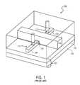
- An example of an proposed SOI transistor which can be operated in a fully depleted manneris a tri-gate transistor 100 , such as illustrated in FIG. 1 .
- Tri-gate transistor 100includes a silicon body 104 formed on insulating substrate 102 having a buried oxide layer 103 formed on a monocrystalline silicon substrate 105 .
- a gate dielectric layer 106is formed on the top and sidewalls of silicon body 104 as shown in FIG. 1 .
- a gate electrode 108is formed on the gate dielectric layer and surrounds the body 104 on three sides essentially providing a transistor 100 having three gate electrodes (G 1 , G 2 , G 3 ) one on each side of silicon body 104 and one on the top surface of the silicon body 104 .
- a source region 110 and a drain region 112are formed in the silicon body 104 on opposite sides of the gate electrode 108 as shown in FIG. 1 .
- An advantage of the tri-gate transistor 100is that it exhibits good short channel effects (SCE).
- tri-gate transistor 100has good short channel effects is that the nonplanarity of the device places the gate electrode 108 in such a way as to surround the active channel region.
- the external contact resistance (Rext)is increasingly becoming more significant portion of the overall device resistance. This is particularly problematic in three dimensional transistors (formed both by etching of Si wafer, or by chemical synthesis of nanowires), where the source region 110 and drain region 112 are formed in the narrow silicon body 104 .
- standard techniques for reducing contact resistancesuch as by forming “raised” source/drain regions where additional epitaxial silicon is formed on the silicon body 104 is difficult to implement in nonplanar transistors. For example, it is difficult to grow “raised” epitaxial source/drain regions on the sides of the silicon body 104 . For these reasons the devices suffer from high Rext and degraded performance.
- FIG. 1is an illustration of a cross-sectional view of a nonplanar transistor.
- FIG. 2Ais an illustration of an overhead/side view of a nonplanar transistor having a metal source and drain region in accordance with the present invention.
- FIG. 2Bis a cross-sectional view of a transistor illustrated in FIG. 2A taken through the semiconductor body.
- FIG. 3Ais an illustration of an overhead/side view of a nonplanar transistor having a metal source/drain region in accordance with an embodiment of the present invention.
- FIG. 3Bis a cross-sectional view a transistor illustrated in FIG. 3A taken through the semiconductor body.
- FIG. 3Cis a cross-section view of a transistor having a source and drain extension each comprising a metal portion, a doped semiconductor contact portion and an extension portion.
- FIGS. 4A-4Lillustrate a method of forming a nonplanar transistor having metal portions of a source and drain regions in accordance with embodiment of the present invention.
- the present inventionis a field effect transistor with metal source/drain regions and its method of fabrication.
- numerous specific detailsare set forth in order to provide a thorough understanding of the present invention.
- well known semiconductor processes and manufacturing techniqueshave not been described in particular detail in order to not unnecessarily obscure the present invention.
- a metal oxide semiconductor field effect transistorhaving a pair of source/drain regions which each comprise a semiconductor portion and a metal portion.
- a replacement source/drain techniqueis used to etch away a portion of the doped source/drain regions so that they can be replaced with a high conductivity metal, such as platinum and palladium. In this way, a lower R-external may be achieved since the metallic interconnect extends much closer towards the channel region.
- the metal portion of the source/drain regionis made extremely close to the channel region such that the metal is formed adjacent to and in contact with the tip or source/drain extension portion of the source and drain regions.
- the source region and drain regionBy forming the source region and drain region with a metal portion and a semiconductor portion allows for the scalable switching of the PNP or NPN junctions while bringing the high conductivity metal source/drain electrodes as close to the channel region as possible. In this way, the metal source and drain regions can extend all the way to the tips of the transistor enhancing the external conductivity while circumventing known disadvantages of metal source/drains in direct contact with the channel material (e.g., ambipolar conduction).
- the source/drain structure of the present inventionis ideally suited for use in very small width and narrow transistors, such as nonplanar devices, the present invention can be utilized in any transistor where its small size or dimensions causes the transistor to have a high R-external.
- FIGS. 2A and 2BAn example of a transistor 200 having source/drain regions with metal portions in accordance with an embodiment of the present invention is illustrated in FIGS. 2A and 2B .
- FIG. 2Ais an illustration of an overhead/side view of transistor 200 while FIG. 2B is an illustration of a cross-sectional view of transistor 200 taken through the semiconductor body.
- Transistor 200includes a semiconductor body 204 , such as an epitaxial silicon body, formed on an insulating substrate 202 .
- the semiconductor bodyhas top surface opposite a bottom surface formed on an insulating substrate and a pair of laterally opposite sidewalls.
- the semiconductor bodyhas a height which is approximately equal to its width.
- a gate dielectric layer 206is formed on the top surface and sidewalls of the semiconductor body 204 as shown in FIG. 2A .
- a gate electrode 208is formed on and around the gate dielectric layer 206 formed on the top surface and sidewalls of the semiconductor body 204 .
- the gate electrode 208surrounds the channel region 210 of the semiconductor body 204 illustrated in FIG. 2A .
- a source region 212 and a drain region 214are formed in the semiconductor body 204 on opposite sides of the gate electrode 208 as shown in FIGS. 2A and 2B .
- the source region 212includes a metal portion 216 and a doped semiconductor portion 218 and drain region 214 includes a metal portion 220 and a doped semiconductor portion 222 .
- the portion of the semiconductor body 204 located between the source region 212 and drain region 214defines a channel region 210 of transistor 200 .
- the doped semiconductor portions 218 and 222contact the channel region 210 of the semiconductor device.
- the metal portions 216 and 220 of the source and drain regions 212 and 214respectively, extend as close as possible to the channel region 210 without actually contacting the channel region.
- the metal portion 216 and 220are offset from the channel region 210 by doped semiconductor portions 218 and 222 by approximately 5 nanometers.
- the doped semiconductor regionshave a doping concentration of between 1e20 and 1e21/cm 3 .
- the doped semiconductor portions 218 and 222are doped to the opposite conductivity type than the dopant conductivity of the channel region 210 of the semiconductor body 204 .
- metal regions 216 and 220 and the doped semiconductor regions 218 and 222 of the source and drain regions 212 and 214extend completely through the semiconductor body 204 and contact the insulating substrate 202 .
- the metal portions 216 and 220are formed from a high conductivity metal.
- the metal portion 216 for the source region 212 and the metal portion 220 of the drain region 214are formed from a material which forms favorable “Schottky barrier” properties with doped semiconductor portions 218 and 222 of the source and drain regions.
- semiconductor portions 218 and 222are silicon the metal portion may be platinum.
- semiconductor 218 and 222are carbon nanotubes the metal portions may be palladium.
- the metal portions 216 and 220 of the source region 212 and drain region 214can be a metal, such as but not limited to palladium and platinum.
- the metal portions of the source and drain regioncan be fabricated from a metal, such as but not limited to aluminum and titanium. It is to be appreciated that the source region 212 and drain region 214 can be collectively referred to as a pair of source/drain regions.
- an interlayer dielectric layer 230such as but not limited to a silicon dioxide layer or a low-K dielectric, such as a fluorine doped silicon dioxide, a carbon doped oxide layer or a zeolite dielectric layer is formed over and around transistor 200 .
- the interlayer dielectric layer 230isolates transistor 200 from the upper levels of metallization used to interconnect the various transistors 200 formed on substrate 202 into functional integrated circuits, such as microprocessors, digital signal processors and memory devices.
- Metal plugs 232 and 234are formed through the interlayer dielectric layer 230 and contact the metal portions 216 and 220 of the source and drain regions so electrical contact can be made thereto.
- transistor 200can further include a pair of sidewall spacers 302 which are formed along and adjacent to the laterally opposite sidewalls of gate electrode 208 .
- Sidewall spacers 302can be formed from any suitable insulating layer, such as but not limited to silicon dioxide, silicon nitride or composite stack thereof.
- spacers 302have a width of between 5-20 nanometers.
- transistor 200includes a source extension or tip 304 and a drain extension or tip region 306 .
- the source extension region 304 and drain extension region 306are formed in the semiconductor body and are doped to n type conductivity for an NFET and doped to a p type conductivity for a PFET.
- the source and drain extensionsare located beneath the sidewall spacers and extend slightly beneath the sidewalls of the gate electrode 208 .
- the source extension and drain extensionhave a doping concentration level of between 5e19-5e20/cm 3 .
- the metal portion 216 of the source region 212 and the metal portion 220 of the drain region 214extend slightly beneath the sidewall spacers and are in contact with the source and drain extension regions 304 and 306 , respectively, as shown in FIG. 3B .
- isolation regions 307are formed on insulating substrate 202 in order to isolate transistor 200 from adjacent transistors formed on substrate 202 .
- Isolation regions 307can be formed from an insulating oxide film, such as silicon dioxide.
- the metal portion 216 of the source region 212 and the metal portion 220 of the drain region 214are formed in contact with isolation region 306 as well as in contact with the source and drain extension regions 304 and 306 , respectively.
- the source region 212further includes a source contact region 314 and a drain contact region 316 formed in semiconductor body 204 .
- the source and drain contact regions 314 and 316are heavily doped regions. Heavily doped contact region 314 and 316 are doped to the same conductivity type as the source and drain extensions 304 and 306 , but are typically doped to a higher concentration level. In an embodiment of the present invention, the source and drain contact region have a doping concentration between 1e20-1e21/cm 3 .
- the heavily doped source and drain contact region 314 and 316are formed between the source/drain extension regions 304 and 306 , and the metal portions 216 and 220 as illustrated in FIG. 3C .
- the metal portion 216 of the source region 212is formed in direct contact with the heavily doped source contact region 314 and the metal portion 220 of the drain region 214 is in direct contact with the heavily doped drain contact region 316 as illustrated in FIG. 3C .
- Gate electrode 208can be formed of any suitable gate electrode material.
- gate electrode 208comprises a polycrystalline silicon doped to a concentration density between 1 ⁇ 10 19 to 1 ⁇ 10 20 atom/cm 3 .
- the gate electrodecan be a metal gate electrode, such as but not limited to tungsten, tantalum, titanium and their nitrides.
- the gate electrodeis formed from a material having a midgap work function between 4.6 to 4.8 eV. It is to be appreciated, that gate electrode 208 need not necessarily be a single material and can be a composite stack of thin films, such as but not limited to a polycrystalline silicon/metal electrode or a metal/polycrystalline silicon electrode.
- Semiconductor body 204can be formed of any well known semiconductor material, such as but not limited to silicon (Si), germanium (Ge), silicon germanium (Si x Ge y ), gallium arsenide (GaAs), InSb, GaP, GaSb, and carbon nanotubes.
- Semiconductor body 204can be formed of any well known material which can be reversely altered from an insulating state to a conductive state by applying external electrical controls.
- Semiconductor body 204is ideally a single crystalline film when the best electrical performance of transistor 200 is desired.
- semiconductor body 204is a single crystalline film when transistor 200 is used in high performance applications, such as a high density circuit, such as microprocessors.
- Semiconductor body 204can be a polycrystalline film when transistor 200 is used in applications requiring less stringent performance, such as in liquid crystal displays.
- substrate 202is an insulating substrate which includes a lower monocrystalline silicon substrate 201 upon which is formed in insulating layer 203 , such as silicon dioxide film.
- Transistor 200can be formed on any well known insulating substrate, such as a substrate formed from silicon dioxide, nitrides, oxides and sapphires.
- substrate 202can be a semiconductor substrate, such as but not limited to a monocrystalline silicon substrate and a gallium arsenide substrate.
- the channel region 210is intrinsic or undoped monocrystalline silicon. In an embodiment of the present invention, the channel region 210 is doped monocrystalline silicon. When channel region 210 is doped, it is typically doped to a conductivity level between 1 ⁇ 10 16 to 1 ⁇ 10 19 atom/cm 3 . When channel region 210 is doped, it is typically doped to the opposite conductivity type of the doped semiconductor portion of the source region 212 and the doped semiconductor portion drain region 214 .
- Gate dielectric layer 206is formed on and around the sides of semiconductor body 204 as shown in FIG. 2A .
- Gate dielectric layer 206can be any well known gate dielectric layer.
- the gate dielectric layeris a silicon dioxide (SiO 2 ), silicon oxynitride (SiO x N y ), or a silicon nitride (Si 3 N 4 ) dielectric layer.
- the gate dielectric layer 206is a silicon oxynitride film formed to a thickness between 5-20 ⁇ .
- gate dielectric 206is a high k gate dielectric layer, such as a metal oxide dielectric, such as but not limited to tantalum pentaoxide, titanium oxide, hafnium oxide, zirconium oxide, aluminum oxide and various silicates or other high k dielectrics, such as lead zirconate titanate (BZT) and barium strontium titanate (BST).
- FIGS. 4A-4LA method of fabricating a field effect transistor with source and drain regions having metal portions in accordance with embodiments of the present invention is illustrated in FIGS. 4A-4L .
- the fabrication of the field effect transistorbegins with a substrate 402 .
- a silicon or semiconductor film 408is formed on substrate 402 as shown in FIG. 4A .
- the substrate 402is an insulating substrate such as shown in FIG. 4A .
- insulating substrate 402includes a lower monocrystalline silicon substrate 404 and a top insulating layer 406 , such as a silicon dioxide film or silicon nitride film. Insulating layer 406 isolates semiconductor film 408 from substrate 404 and in an embodiment is formed to a thickness between 200-2000 ⁇ .
- Insulating layer 406is sometimes referred to as “a buried oxide” layer.
- a silicon or semiconductor film 408is formed on an insulating substrate 402 , a silicon or semiconductor-on-insulator (SOI) substrate is created.
- substrate 402can be a semiconductor substrate, such as but not limited to a silicon monocrystalline substrate and a gallium arsenide substrate.
- semiconductor film 408is ideally a silicon film, in other embodiments it can be other types of semiconductor films, such as but not limited to germanium, silicon germanium, gallium arsenide, InSb, GaP, GaSb as well as carbon nanotubes.
- semiconductor film 408is an intrinsic (i.e., undoped) silicon film. In other embodiments, semiconductor film 408 is doped to a p type or n type conductivity with a concentration level between 1 ⁇ 10 16 to 1 ⁇ 10 19 atoms/cm 3 . Semiconductor film 408 can be insitu doped (i.e., doped while it is deposited) or doped after it is formed on substrate 402 by, for example, ion implantation. Doping after formation enables both PFET and NFET devices to be fabricated easily on the same insulating substrate. The doping level of the semiconductor film 408 determines the doping level of the channel region of the device.
- semiconductor film 408is formed to a thickness which is approximately equal to the height desired for the subsequently formed semiconductor body or bodies of the fabricated transistor. In embodiments of the present invention, semiconductor film 408 has a thickness or height 409 of less than 30 nanometers and ideally less than 20 nanometers. In an embodiment of the present invention, semiconductor film 408 is formed to a thickness approximately equal to the gate “length” desired of the fabricated transistor. In an embodiment of the present invention, semiconductor film 408 is formed thicker than the desired gate length of the device. In an embodiment of the present invention, a semiconductor film 408 is formed to a thickness which will enable the fabricated transistor to be operated in a fully depleted manner for a desired gate length (Lg).
- Lgdesired gate length
- Semiconductor film 408can be formed on insulating substrate 402 in any well known method.
- a silicon-on-insulator substrateknown as the “SIMOX” technique
- oxygen atomsare implanted at a high dose into a single crystalline silicon substrate and then annealed to form the buried oxide 406 within the substrate.
- the portion of the single crystalline silicon substrate above the buried oxidebecomes a silicon film.
- an epitaxial silicon film transfer techniquewhich is generally referred to as bonded SOI may be utilized to form a SOI substrate.
- isolation regions 410can be formed in the semiconductor film 408 to isolate the various transistors formed in semiconductor film 408 from one another. Isolation regions 410 can be formed by etching away portions of the semiconductor film 408 adjacent to the transistor fabrication area 412 in semiconductor film 408 . Well know photolithography and etching techniques can be used to remove the semiconductor film at locations where isolation regions 410 are desired. An insulating film, such as but not limited to silicon dioxide, can then be blanket deposited into the areas where the semiconductor film 408 has been etched out as well as on over the semiconductor film 408 in the device fabrication area 412 .
- the deposited insulating filmcan then be polished back by, for example, chemical mechanical polishing (CMP) to remove the insulating film from the device fabrication area 412 and thereby form isolation regions 410 which are planar with the top surface of the semiconductor film 408 in the device fabrication area 412 .
- CMPchemical mechanical polishing
- Other well known and suitable techniquesmay be utilized to form isolation regions 410 .
- a semiconductor body 414is formed from semiconductor film 408 as shown in FIG. 4C .
- Semiconductor body 414can be formed by forming a photoresist mask over the locations of semiconductor film 408 where a semiconductor body 414 is desired.
- a photoresist maskcan be formed with well known photolithography techniques including masking, exposing and developing a blanket deposited photoresist film.
- Semiconductor film 408would then be etched in alignment with the photoresist mask to form semiconductor body 414 .
- Any well known semiconductor etching techniques, such as anisotropic plasma etching or reactive ion etching,can be used to etch semiconductor film 408 in alignment with the photoresist mask to form semiconductor body 414 .
- the semiconductor bodyis etched so that it has a width (i.e. distance between laterally opposite sidewalls) which is approximately equal to its height.
- a gate dielectric layer 416is formed on and around semiconductor body 414 .
- the gate dielectric layer 416is formed on a top surface of the semiconductor body as well as on the laterally opposite sidewalls of the semiconductor body 414 .
- the gate dielectric layer 416can be a deposited dielectric or a grown dielectric.
- the gate dielectric layer 416is a silicon dioxide dielectric film grown with a dry/wet oxidation process.
- the silicon oxide filmis grown to a thickness between 5-15 ⁇ .
- the gate dielectric layeris deposited dielectric, such as but not limited to a high dielectric constant film, such as a metal oxide dielectric, such as tantalum pentaoxide, titanium oxide, hafnium oxide, zirconium oxide, aluminum oxide and various silicates or other high k dielectrics, such as lead zirconate titanate (BZT) and barium strontium titanate (BST).
- a high dielectric constant filmcan be formed by any well known technique, such as but not limited to chemical vapor deposition (CVD) and atomic layer deposition (ALD).
- Gate electrode 418is formed on gate dielectric layer 416 formed on the top surface of semiconductor body 414 and is formed on or adjacent to the gate dielectric layer 416 formed on or adjacent to the sidewall of the semiconductor body 414 as shown in FIG. 4D .
- the gate electrode 418has a top surface opposite a bottom surface formed on insulating substrate 402 and has a pair of laterally opposite sidewalls which run perpendicular to the sidewalls of semiconductor body 414 .
- Gate electrode 418can be formed by blanket depositing a suitable gate electrode material to a thickness between 200-3000 ⁇ .
- the gate electrode materialis then patterned with well known photolithography and etching techniques to form a gate electrode 418 from the gate electrode material.
- the gate electrode materialcomprises a polycrystalline silicon.
- the gate electrode materialcomprises a polycrystalline silicon germanium alloy.
- the gate electrode materialcan comprise a metal film, such as tungsten, tantalum and their nitrides. Alternatively, to a substractive approach for forming the gate electrode 418 , other techniques may be utilized.
- the source and drain regionseach comprise a doped semiconductor portion and a metal portion.
- the semiconductor portions of the source/drain regionscan be formed.
- the doped semiconductor portionsinclude tip or source/drain extension regions.
- Source and drain extension regions 420 and 422can be formed by placing dopants into the semiconductor body 414 on both sides of gate electrode 418 as shown in FIG. 4E .
- the semiconductor bodyis doped to a p type conductivity and to a concentration of between 1 ⁇ 10 20 -1 ⁇ 10 21 atoms/cm 3 .
- the semiconductor bodyis doped with n type conductivity ions to a concentration between 1 ⁇ 10 20 -1 ⁇ 10 21 atoms/cm 3 .
- the silicon bodyis doped by ion implantation.
- the ion implantationoccurs in a vertical direction (i.e., a direction perpendicular to substrate 402 ) as shown in FIG. 4E .
- gate electrode 418is a polysilicon gate electrode, it can be doped during the ion implantation process. Gate electrode 418 acts as a mask to prevent the ion implantation step from doping the channel region 421 of the transistor.
- the channel region 421is the portion of the semiconductor body 414 located beneath or surrounded by gate electrode 418 .
- other methodssuch as solid source diffusion may be used to dope the semiconductor body 414 to the source and drain extension regions 420 and 422 .
- dielectric sidewall spacers 424can be formed on the sidewalls of gate electrode 418 .
- Sidewall spacerscan be used to offset heavy source/drain contact implants.
- Spacerscan be formed by blanket depositing a conformal dielectric film, such as but not limited to silicon nitride, silicon oxide, silicon oxynitride or combinations thereof over the substrate of FIG. 4E .
- the spacer dielectric filmis deposited in a conformal manner so that it forms to substantially equal thickness on vertical surfaces, such as sidewalls of the gate electrode 418 as well as on horizontal surfaces, such as on the top surface of silicon body 414 and gate electrode 418 .
- the dielectric filmis a silicon nitride film formed by a hot wall lower pressure chemical vapor deposition (LPCVD) process.
- LPCVDhot wall lower pressure chemical vapor deposition
- the deposited thickness of the dielectric filmdetermines the width or thickness of the formed spacers.
- the spacer dielectric filmis formed to a thickness between 20-200 ⁇ .
- the spacer dielectric filmcan then be anisotropically etched by, for example, plasma etching or reactive ion etching to form sidewall spacers 424 .
- the anisotropic etchremoves the dielectric film from horizontal surfaces and leaves the dielectric sidewall spacers adjacent to vertical surfaces, such as the sidewalls of gate electrode 418 .
- the resultis the formation of sidewall spacers 424 which run along the laterally opposite sidewalls of gate electrode 418 as shown in FIG. 4F .
- Heavily doped source/drain contact regionscan be formed by ion implantation with a vertical ion implantation process.
- the ion implantation processdopes the semiconductor body 414 located adjacent to the sidewall spacers to a concentration between 1 ⁇ 10 20 -1 ⁇ 10 21 atoms/cm 3 to form source contact region 426 and drain contact region 428 .
- Sidewall spacers 424offset the source/drain contact implantation step and define the tip regions as the regions of the doped semiconductor body 414 beneath sidewall spacers 424 .
- the contact regionsare the regions of the semiconductor body which are adjacent to the outside edges of the sidewall spacers 424 .
- an interlayer dielectric (ILD) 430is blanket deposited over the substrate as shown in FIG. 4H .
- the interlayer dielectricmay be referred to as ILD0 because it is used to isolate the transistor from a subsequently formed first level of metallization.
- the interlayer dielectric (ILD) 430is formed above isolation regions 410 and over and above gate electrode 418 as well as above and around the exposed portion of semiconductor body 414 .
- the interlayer dielectric 430fills the gap made between semiconductor body 414 , isolation region 410 and the gate electrode/sidewall spacers 424 / 418 .
- Interlayer dielectric 430is formed to a thickness sufficient to isolate gate electrode 418 and semiconductor body 414 from a first level of metallization subsequently formed on the top surface of the interlayer dielectric 430 .
- the interlayer dielectric 430is formed to a thickness between 100 and 500 nm.
- Interlayer dielectric 430can be formed from any suitable dielectric material, such as silicon dioxide, which can be used as an interlayer dielectric. Additionally, interlayer dielectric 430 need not be a single dielectric film and can be a composite dielectric formed from two or more dielectric layers.
- a stress providing layersuch as silicon nitride
- the interlayer dielectric 430can be a low k dielectric (i.e., have a dielectric constant less than the dielectric constant of silicon dioxide which is approximately 4.0) in order to prevent capacitance coupling between adjacent contacts.
- an interlayer dielectricis formed from a low k material, such as but not limited to fluorine doped SiO 2 , a carbon doped oxide (CDO), polymides, and zeolites.
- ILD 430is formed of a material which can be selectively etched with respect to semiconductor body 414 so that an opening can be etched into the semiconductor body without laterally etching into ILD 430 adjacent to the sidewalls of the semiconductor body 414 .
- interlayer dielectric 430is formed from the same material, such as silicon dioxide, which is used to form isolation regions 410 .
- the dielectric layercan be planarized by, for example, chemical mechanical planarization in order to form the interlayer dielectric 430 with a planar top surface. Any suitable technique can be used to deposit the interlayer dielectric 430 , such as but not limited to chemical vapor deposition (CVD) and high density plasma (HDP) CVD.
- CVDchemical vapor deposition
- HDPhigh density plasma
- FIGS. 4I-4Lillustrate a cross-sectional view taken through the semiconductor body 414 as set forth in FIG. 4H .
- a pair of contact opening 434 and 436is formed through interlayer dielectric and down to the source contact region 426 and the drain contact 428 of semiconductor body 414 .
- Well known photolithography techniquescan be used to form a photoresist mask to define the locations where openings 434 and 436 are to be formed and then well know etching techniques can be used to etch the openings 434 and 436 .
- Any well known and suitable etching techniqueincluding dry etching and wet etching may be used to form openings 434 and 436 .
- an etchantcomprising HF may be used.
- the etchant used to form contact openings 434 and 436is selective semiconductor 414 so that it can etch through the interlayer dielectric 430 and essentially stop etching on the semiconductor body 414 .
- an etchant which has an etch selectivity ratio between silicon dioxide and silicon of at least 10:1is used.
- openings 440 and 442are etched into semiconductor body 414 .
- the semiconductor body etchantetches laterally towards the channel of the device.
- the etching of the openings 440 and 442is continued until the tip or extension portions 420 and 422 of the source and drain regions are reached as illustrated in FIG. 4J .
- the etchingmay not quite reach the tip portions 420 and 422 of the source and drain regions and may leave a portion of the heavily doped source/drain contact regions 426 and 428 as discussed earlier.
- the openings 440 and 442are etched vertically downward until they reach buried oxide layer 406 as illustrated in FIG. 4J . Additionally, in an embodiment of the present invention, the openings are etched laterally or horizontally outward until isolation regions 410 are reached as illustrated in FIG. 4J . In an embodiment of the present invention, the openings 440 and 442 are etched with an etchant which has a high selectivity to interlayer dielectric 430 , isolations regions 410 and buried oxide layer 406 . That is an etchant is used which etches semiconductor body 414 but not interlayer dielectric 430 , isolation regions 410 or buried oxide layer 406 .
- openings 440 and 442are securely contained between buried oxide layer 406 , the isolation region 410 and the interlayer dielectric 430 as illustrated in FIG. 4J .
- Any suitable wet or dry etching techniquesmay be utilized to form openings 440 and 442 .
- the etching processshould be substantially isotropic in order to provide for lateral undercutting of openings 434 and 436 as illustrated in FIG. 4J .
- the silicon bodycan be etched to form openings 440 and 442 with an etchant comprising KOH.
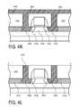
- openings 440 and 442 formed in semiconductor body 414 and contact openings 434 and 436are filled with a metal film 443 to form source and drain contacts 444 and 446 and the metal portions 450 and 452 of the source and drain regions.
- the source and drain metal portions 450 and 452make direct contact with highly doped semiconductor portion of the source and drain regions.
- the doped semiconductor portionis the tip or source/drain extension regions 420 and 422 .
- the metal portions 450 and 452make direct contact with the heavily doped source and drain contact regions 426 and 428 .
- metal portions 450 and 452are formed directly onto the buried oxide layer 406 and in an embodiment of the present invention, in contact the outside portions of isolation regions 410 as illustrated in FIG. 4K .
- the metal 443is formed by a conformal deposition process so that the contact openings 440 and 442 formed in the semiconductor body 414 can be completely filled with the metal film.
- a blanket deposition of a conformal metal filmby, for example, chemical vapor deposition (CVD) or atomic layer deposition (ALD) will also deposit the film onto the top surface of the interlayer dielectric layer 430 as illustrated in FIG. 4K .
- the metal film 443is a low resistance, high conductivity metal film.
- the metal film 443is a film which can form a Schottky contact with the doped semiconductor portion of the semiconductor body.
- the metal filmwhen forming an NFET type device, can be a metal selected from the group consisting of aluminum and titanium.
- the metal filmwhen forming PFET type device, can be a metal selected from the group consisting of palladium and platinum.
- the metal filmwhen semiconductor body is formed from silicon the metal film can be platinum.
- the metal filmwhen the semiconductor body is formed from carbon nanotubes, the metal film can comprise palladium and aluminum.
- the metal film 443 formed on the top surface of the interlayer dielectric 430is removed by well known techniques.
- Metal film 443 on the top surface of the interlayer dielectric area 430can be removed by, for example, chemical mechanical planarization or by a plasma etch back process. This completes the fabrication of a field effect transistor having source and drain regions with metal portions to improve external resistance (Rext) of the device.
- the present inventionhas been described with respect to a nonplanar transistor, such as a tri-gate transistor, the present invention is not to be limited to these types if transistors.
- the present inventionis equally applicable to the formation of source and drain regions of a planar transistor where the gate electrode and gate dielectric layer are formed on a single surface of semiconductor film as is well know in the art.
- the present inventionis equally applicable to FINFET devices or dual gate devices where the gate electrode/gate dielectric is formed on two sides of the semiconductor body and not on the top surface of the semiconductor body as is well known in the art.
Landscapes
- Engineering & Computer Science (AREA)
- Physics & Mathematics (AREA)
- Condensed Matter Physics & Semiconductors (AREA)
- General Physics & Mathematics (AREA)
- Computer Hardware Design (AREA)
- Microelectronics & Electronic Packaging (AREA)
- Power Engineering (AREA)
- Manufacturing & Machinery (AREA)
- Thin Film Transistor (AREA)
- Insulated Gate Type Field-Effect Transistor (AREA)
Abstract
Description
This application is a divisional of U.S. patent application Ser. No. 11/080,765, filed Mar. 14, 2005, now abandoned (U.S. Patent Application Publication No. US 2006-0202266), published Sep. 14, 2006, the entire contents of which are hereby incorporated by reference herein.
1. Field of the Invention
The present invention relates to the field of semiconductor devices and more particularly to a semiconductor device having a source/drain region comprising a semiconductor portion and a metal portion.
2. Discussion of Related Art
In order to increase the performance of modern integrated circuits, such as microprocessors, silicon on insulator (SOI) transistors have been proposed. Silicon on insulator (SOI) transistors have an advantage in that they can be operated in a fully depleted manner. Fully depleted transistors have an advantage of an ideal subthreshold gradient for optimized on-current/off-current ratios. An example of an proposed SOI transistor which can be operated in a fully depleted manner is a tri-gatetransistor 100, such as illustrated inFIG. 1 .Tri-gate transistor 100 includes asilicon body 104 formed oninsulating substrate 102 having a buriedoxide layer 103 formed on amonocrystalline silicon substrate 105. A gatedielectric layer 106 is formed on the top and sidewalls ofsilicon body 104 as shown inFIG. 1 . Agate electrode 108 is formed on the gate dielectric layer and surrounds thebody 104 on three sides essentially providing atransistor 100 having three gate electrodes (G1, G2, G3) one on each side ofsilicon body 104 and one on the top surface of thesilicon body 104. Asource region 110 and adrain region 112 are formed in thesilicon body 104 on opposite sides of thegate electrode 108 as shown inFIG. 1 . An advantage of the tri-gatetransistor 100 is that it exhibits good short channel effects (SCE). One reason tri-gatetransistor 100 has good short channel effects is that the nonplanarity of the device places thegate electrode 108 in such a way as to surround the active channel region. Unfortunately, as tri-gate devices become increasingly smaller, the external contact resistance (Rext) is increasingly becoming more significant portion of the overall device resistance. This is particularly problematic in three dimensional transistors (formed both by etching of Si wafer, or by chemical synthesis of nanowires), where thesource region 110 anddrain region 112 are formed in thenarrow silicon body 104. Unfortunately, standard techniques for reducing contact resistance, such as by forming “raised” source/drain regions where additional epitaxial silicon is formed on thesilicon body 104 is difficult to implement in nonplanar transistors. For example, it is difficult to grow “raised” epitaxial source/drain regions on the sides of thesilicon body 104. For these reasons the devices suffer from high Rext and degraded performance.
The present invention is a field effect transistor with metal source/drain regions and its method of fabrication. In the following description, numerous specific details are set forth in order to provide a thorough understanding of the present invention. In other instances, well known semiconductor processes and manufacturing techniques have not been described in particular detail in order to not unnecessarily obscure the present invention.
In embodiments of the present invention, include a metal oxide semiconductor field effect transistor having a pair of source/drain regions which each comprise a semiconductor portion and a metal portion. In an embodiment of the present invention, a replacement source/drain technique is used to etch away a portion of the doped source/drain regions so that they can be replaced with a high conductivity metal, such as platinum and palladium. In this way, a lower R-external may be achieved since the metallic interconnect extends much closer towards the channel region. In an embodiment of the present invention, the metal portion of the source/drain region is made extremely close to the channel region such that the metal is formed adjacent to and in contact with the tip or source/drain extension portion of the source and drain regions. By forming the source region and drain region with a metal portion and a semiconductor portion allows for the scalable switching of the PNP or NPN junctions while bringing the high conductivity metal source/drain electrodes as close to the channel region as possible. In this way, the metal source and drain regions can extend all the way to the tips of the transistor enhancing the external conductivity while circumventing known disadvantages of metal source/drains in direct contact with the channel material (e.g., ambipolar conduction). Although the source/drain structure of the present invention is ideally suited for use in very small width and narrow transistors, such as nonplanar devices, the present invention can be utilized in any transistor where its small size or dimensions causes the transistor to have a high R-external.
An example of atransistor 200 having source/drain regions with metal portions in accordance with an embodiment of the present invention is illustrated inFIGS. 2A and 2B .FIG. 2A is an illustration of an overhead/side view oftransistor 200 whileFIG. 2B is an illustration of a cross-sectional view oftransistor 200 taken through the semiconductor body.Transistor 200 includes asemiconductor body 204, such as an epitaxial silicon body, formed on aninsulating substrate 202. The semiconductor body has top surface opposite a bottom surface formed on an insulating substrate and a pair of laterally opposite sidewalls. In an embodiment of the present invention, the semiconductor body has a height which is approximately equal to its width. A gatedielectric layer 206 is formed on the top surface and sidewalls of thesemiconductor body 204 as shown inFIG. 2A . Agate electrode 208 is formed on and around the gatedielectric layer 206 formed on the top surface and sidewalls of thesemiconductor body 204. Thegate electrode 208 surrounds thechannel region 210 of thesemiconductor body 204 illustrated inFIG. 2A .
Asource region 212 and adrain region 214 are formed in thesemiconductor body 204 on opposite sides of thegate electrode 208 as shown inFIGS. 2A and 2B . Thesource region 212 includes ametal portion 216 and adoped semiconductor portion 218 and drainregion 214 includes ametal portion 220 and adoped semiconductor portion 222. The portion of thesemiconductor body 204 located between thesource region 212 and drainregion 214 defines achannel region 210 oftransistor 200. The dopedsemiconductor portions channel region 210 of the semiconductor device. In an embodiment of the present invention, themetal portions regions channel region 210 without actually contacting the channel region. In an embodiment of the present invention, themetal portion channel region 210 by dopedsemiconductor portions semiconductor portions channel region 210 of thesemiconductor body 204. In an embodiment of the present invention,metal regions semiconductor regions regions semiconductor body 204 and contact the insulatingsubstrate 202. In an embodiment of the present invention, themetal portions metal portion 216 for thesource region 212 and themetal portion 220 of thedrain region 214 are formed from a material which forms favorable “Schottky barrier” properties with dopedsemiconductor portions semiconductor portions semiconductor metal portions source region 212 and drainregion 214 can be a metal, such as but not limited to palladium and platinum. In an embodiment of the present invention, when forming NFET (an n type field effect transistor) where the doped source and drain regions are doped to an n type conductivity and the majority carriers are electrons, the metal portions of the source and drain region can be fabricated from a metal, such as but not limited to aluminum and titanium. It is to be appreciated that thesource region 212 and drainregion 214 can be collectively referred to as a pair of source/drain regions.
As shown inFIGS. 2A and 2B , aninterlayer dielectric layer 230, such as but not limited to a silicon dioxide layer or a low-K dielectric, such as a fluorine doped silicon dioxide, a carbon doped oxide layer or a zeolite dielectric layer is formed over and aroundtransistor 200. Theinterlayer dielectric layer 230 isolatestransistor 200 from the upper levels of metallization used to interconnect thevarious transistors 200 formed onsubstrate 202 into functional integrated circuits, such as microprocessors, digital signal processors and memory devices. Metal plugs232 and234 are formed through theinterlayer dielectric layer 230 and contact themetal portions
In an embodiment of the present invention, as illustrated inFIGS. 3A and 3B ,transistor 200 can further include a pair ofsidewall spacers 302 which are formed along and adjacent to the laterally opposite sidewalls ofgate electrode 208.Sidewall spacers 302 can be formed from any suitable insulating layer, such as but not limited to silicon dioxide, silicon nitride or composite stack thereof. In an embodiment of the present invention,spacers 302 have a width of between 5-20 nanometers. In an embodiment of the present invention,transistor 200 includes a source extension ortip 304 and a drain extension ortip region 306. Thesource extension region 304 anddrain extension region 306 are formed in the semiconductor body and are doped to n type conductivity for an NFET and doped to a p type conductivity for a PFET. The source and drain extensions are located beneath the sidewall spacers and extend slightly beneath the sidewalls of thegate electrode 208. In an embodiment of the present invention, the source extension and drain extension have a doping concentration level of between 5e19-5e20/cm3. In an embodiment of the present invention, themetal portion 216 of thesource region 212 and themetal portion 220 of thedrain region 214 extend slightly beneath the sidewall spacers and are in contact with the source anddrain extension regions FIG. 3B .
In an embodiment of the present invention,isolation regions 307 are formed on insulatingsubstrate 202 in order to isolatetransistor 200 from adjacent transistors formed onsubstrate 202.Isolation regions 307 can be formed from an insulating oxide film, such as silicon dioxide. In an embodiment of the present invention, themetal portion 216 of thesource region 212 and themetal portion 220 of thedrain region 214 are formed in contact withisolation region 306 as well as in contact with the source anddrain extension regions
In an embodiment of the present invention, thesource region 212 further includes asource contact region 314 and adrain contact region 316 formed insemiconductor body 204. The source and draincontact regions contact region extensions contact region drain extension regions metal portions FIG. 3C . As such, in an embodiment of the present invention, themetal portion 216 of thesource region 212 is formed in direct contact with the heavily dopedsource contact region 314 and themetal portion 220 of thedrain region 214 is in direct contact with the heavily dopeddrain contact region 316 as illustrated inFIG. 3C .
In an embodiment of the present invention,substrate 202 is an insulating substrate which includes a lowermonocrystalline silicon substrate 201 upon which is formed in insulatinglayer 203, such as silicon dioxide film.Transistor 200, however, can be formed on any well known insulating substrate, such as a substrate formed from silicon dioxide, nitrides, oxides and sapphires. In an embodiment of the present invention,substrate 202 can be a semiconductor substrate, such as but not limited to a monocrystalline silicon substrate and a gallium arsenide substrate.
In an embodiment of the present invention, thechannel region 210 is intrinsic or undoped monocrystalline silicon. In an embodiment of the present invention, thechannel region 210 is doped monocrystalline silicon. Whenchannel region 210 is doped, it is typically doped to a conductivity level between 1×10¹⁶to 1×10¹⁹atom/cm3. Whenchannel region 210 is doped, it is typically doped to the opposite conductivity type of the doped semiconductor portion of thesource region 212 and the doped semiconductorportion drain region 214.
A method of fabricating a field effect transistor with source and drain regions having metal portions in accordance with embodiments of the present invention is illustrated inFIGS. 4A-4L . The fabrication of the field effect transistor begins with asubstrate 402. A silicon orsemiconductor film 408 is formed onsubstrate 402 as shown inFIG. 4A . In an embodiment of the present invention, thesubstrate 402 is an insulating substrate such as shown inFIG. 4A . In an embodiment of the present invention, insulatingsubstrate 402 includes a lowermonocrystalline silicon substrate 404 and a top insulatinglayer 406, such as a silicon dioxide film or silicon nitride film. Insulatinglayer 406 isolatessemiconductor film 408 fromsubstrate 404 and in an embodiment is formed to a thickness between 200-2000 Å. Insulatinglayer 406 is sometimes referred to as “a buried oxide” layer. When a silicon orsemiconductor film 408 is formed on an insulatingsubstrate 402, a silicon or semiconductor-on-insulator (SOI) substrate is created. In other embodiments of the present invention,substrate 402 can be a semiconductor substrate, such as but not limited to a silicon monocrystalline substrate and a gallium arsenide substrate. Althoughsemiconductor film 408 is ideally a silicon film, in other embodiments it can be other types of semiconductor films, such as but not limited to germanium, silicon germanium, gallium arsenide, InSb, GaP, GaSb as well as carbon nanotubes.
In an embodiment of the present invention,semiconductor film 408 is an intrinsic (i.e., undoped) silicon film. In other embodiments,semiconductor film 408 is doped to a p type or n type conductivity with a concentration level between 1×10¹⁶to 1×10¹⁹atoms/cm3.Semiconductor film 408 can be insitu doped (i.e., doped while it is deposited) or doped after it is formed onsubstrate 402 by, for example, ion implantation. Doping after formation enables both PFET and NFET devices to be fabricated easily on the same insulating substrate. The doping level of thesemiconductor film 408 determines the doping level of the channel region of the device. In an embodiment of the present invention,semiconductor film 408 is formed to a thickness which is approximately equal to the height desired for the subsequently formed semiconductor body or bodies of the fabricated transistor. In embodiments of the present invention,semiconductor film 408 has a thickness orheight 409 of less than 30 nanometers and ideally less than 20 nanometers. In an embodiment of the present invention,semiconductor film 408 is formed to a thickness approximately equal to the gate “length” desired of the fabricated transistor. In an embodiment of the present invention,semiconductor film 408 is formed thicker than the desired gate length of the device. In an embodiment of the present invention, asemiconductor film 408 is formed to a thickness which will enable the fabricated transistor to be operated in a fully depleted manner for a desired gate length (Lg).
In an embodiment of the present invention, as shown inFIG. 4B ,isolation regions 410 can be formed in thesemiconductor film 408 to isolate the various transistors formed insemiconductor film 408 from one another.Isolation regions 410 can be formed by etching away portions of thesemiconductor film 408 adjacent to thetransistor fabrication area 412 insemiconductor film 408. Well know photolithography and etching techniques can be used to remove the semiconductor film at locations whereisolation regions 410 are desired. An insulating film, such as but not limited to silicon dioxide, can then be blanket deposited into the areas where thesemiconductor film 408 has been etched out as well as on over thesemiconductor film 408 in thedevice fabrication area 412. The deposited insulating film can then be polished back by, for example, chemical mechanical polishing (CMP) to remove the insulating film from thedevice fabrication area 412 and thereby formisolation regions 410 which are planar with the top surface of thesemiconductor film 408 in thedevice fabrication area 412. Other well known and suitable techniques may be utilized to formisolation regions 410.
Next, asemiconductor body 414 is formed fromsemiconductor film 408 as shown inFIG. 4C .Semiconductor body 414 can be formed by forming a photoresist mask over the locations ofsemiconductor film 408 where asemiconductor body 414 is desired. A photoresist mask can be formed with well known photolithography techniques including masking, exposing and developing a blanket deposited photoresist film.Semiconductor film 408 would then be etched in alignment with the photoresist mask to formsemiconductor body 414. Any well known semiconductor etching techniques, such as anisotropic plasma etching or reactive ion etching, can be used to etchsemiconductor film 408 in alignment with the photoresist mask to formsemiconductor body 414. In an embodiment of the present invention, the semiconductor body is etched so that it has a width (i.e. distance between laterally opposite sidewalls) which is approximately equal to its height.
Next, as shown inFIG. 4D , agate dielectric layer 416 is formed on and aroundsemiconductor body 414. Thegate dielectric layer 416 is formed on a top surface of the semiconductor body as well as on the laterally opposite sidewalls of thesemiconductor body 414. Thegate dielectric layer 416 can be a deposited dielectric or a grown dielectric. In an embodiment of the present invention, thegate dielectric layer 416 is a silicon dioxide dielectric film grown with a dry/wet oxidation process. In an embodiment of the present invention, the silicon oxide film is grown to a thickness between 5-15 Å. In an embodiment of the present invention, the gate dielectric layer is deposited dielectric, such as but not limited to a high dielectric constant film, such as a metal oxide dielectric, such as tantalum pentaoxide, titanium oxide, hafnium oxide, zirconium oxide, aluminum oxide and various silicates or other high k dielectrics, such as lead zirconate titanate (BZT) and barium strontium titanate (BST). A high dielectric constant film can be formed by any well known technique, such as but not limited to chemical vapor deposition (CVD) and atomic layer deposition (ALD).
Next, as also shown inFIG. 4D , agate electrode 418 is formed.Gate electrode 418 is formed ongate dielectric layer 416 formed on the top surface ofsemiconductor body 414 and is formed on or adjacent to thegate dielectric layer 416 formed on or adjacent to the sidewall of thesemiconductor body 414 as shown inFIG. 4D . Thegate electrode 418 has a top surface opposite a bottom surface formed on insulatingsubstrate 402 and has a pair of laterally opposite sidewalls which run perpendicular to the sidewalls ofsemiconductor body 414.Gate electrode 418 can be formed by blanket depositing a suitable gate electrode material to a thickness between 200-3000 Å. The gate electrode material is then patterned with well known photolithography and etching techniques to form agate electrode 418 from the gate electrode material. In an embodiment of the present invention, the gate electrode material comprises a polycrystalline silicon. In an embodiment of the present invention, the gate electrode material comprises a polycrystalline silicon germanium alloy. In yet another embodiment of the present invention, the gate electrode material can comprise a metal film, such as tungsten, tantalum and their nitrides. Alternatively, to a substractive approach for forming thegate electrode 418, other techniques may be utilized.
Next, a pair of source/drain regions are formed in thesemiconductor body 414 on opposite sides ofgate electrode 418. As stated above, the source and drain regions each comprise a doped semiconductor portion and a metal portion. First, the semiconductor portions of the source/drain regions can be formed. In an embodiment of the present invention, the doped semiconductor portions include tip or source/drain extension regions. Source anddrain extension regions semiconductor body 414 on both sides ofgate electrode 418 as shown inFIG. 4E . For a p type transistor, the semiconductor body is doped to a p type conductivity and to a concentration of between 1×10²⁰-1×10²¹atoms/cm3. For an n type transistor, the semiconductor body is doped with n type conductivity ions to a concentration between 1×10²⁰-1×10²¹atoms/cm3. In an embodiment of the present invention, the silicon body is doped by ion implantation. In an embodiment of the present invention, the ion implantation occurs in a vertical direction (i.e., a direction perpendicular to substrate402) as shown inFIG. 4E . Whengate electrode 418 is a polysilicon gate electrode, it can be doped during the ion implantation process.Gate electrode 418 acts as a mask to prevent the ion implantation step from doping thechannel region 421 of the transistor. Thechannel region 421 is the portion of thesemiconductor body 414 located beneath or surrounded bygate electrode 418. In other embodiments or other methods, such as solid source diffusion may be used to dope thesemiconductor body 414 to the source anddrain extension regions
Next, in an embodiment of the present invention,dielectric sidewall spacers 424 can be formed on the sidewalls ofgate electrode 418. Sidewall spacers can be used to offset heavy source/drain contact implants. Spacers can be formed by blanket depositing a conformal dielectric film, such as but not limited to silicon nitride, silicon oxide, silicon oxynitride or combinations thereof over the substrate ofFIG. 4E . The spacer dielectric film is deposited in a conformal manner so that it forms to substantially equal thickness on vertical surfaces, such as sidewalls of thegate electrode 418 as well as on horizontal surfaces, such as on the top surface ofsilicon body 414 andgate electrode 418. In an embodiment of the present invention, the dielectric film is a silicon nitride film formed by a hot wall lower pressure chemical vapor deposition (LPCVD) process. The deposited thickness of the dielectric film determines the width or thickness of the formed spacers. In an embodiment of the present invention, the spacer dielectric film is formed to a thickness between 20-200 Å. The spacer dielectric film can then be anisotropically etched by, for example, plasma etching or reactive ion etching to formsidewall spacers 424. The anisotropic etch removes the dielectric film from horizontal surfaces and leaves the dielectric sidewall spacers adjacent to vertical surfaces, such as the sidewalls ofgate electrode 418. The result is the formation ofsidewall spacers 424 which run along the laterally opposite sidewalls ofgate electrode 418 as shown inFIG. 4F .
Next, if desired, heavy source/drain contact implants can be made to form heavily dopedsemiconductor film 414. Heavily doped source/drain contact regions can be formed by ion implantation with a vertical ion implantation process. The ion implantation process dopes thesemiconductor body 414 located adjacent to the sidewall spacers to a concentration between 1×10²⁰-1×10²¹atoms/cm3to formsource contact region 426 anddrain contact region 428.Sidewall spacers 424 offset the source/drain contact implantation step and define the tip regions as the regions of the dopedsemiconductor body 414 beneathsidewall spacers 424. The contact regions are the regions of the semiconductor body which are adjacent to the outside edges of thesidewall spacers 424.
Next, an interlayer dielectric (ILD)430 is blanket deposited over the substrate as shown inFIG. 4H . The interlayer dielectric may be referred to as ILD0 because it is used to isolate the transistor from a subsequently formed first level of metallization. The interlayer dielectric (ILD)430 is formed aboveisolation regions 410 and over and abovegate electrode 418 as well as above and around the exposed portion ofsemiconductor body 414. Theinterlayer dielectric 430 fills the gap made betweensemiconductor body 414,isolation region 410 and the gate electrode/sidewall spacers 424/418.Interlayer dielectric 430 is formed to a thickness sufficient to isolategate electrode 418 andsemiconductor body 414 from a first level of metallization subsequently formed on the top surface of theinterlayer dielectric 430. In an embodiment of the present invention, theinterlayer dielectric 430 is formed to a thickness between 100 and 500 nm.Interlayer dielectric 430 can be formed from any suitable dielectric material, such as silicon dioxide, which can be used as an interlayer dielectric. Additionally,interlayer dielectric 430 need not be a single dielectric film and can be a composite dielectric formed from two or more dielectric layers. Additionally, prior to the formation ofinterlayer dielectric 430, a stress providing layer, such as silicon nitride, can be formed over and around the transistor in order to place thechannel region 421 of the device under stress to improve the carrier mobility therein. In an embodiment of the present invention, theinterlayer dielectric 430 can be a low k dielectric (i.e., have a dielectric constant less than the dielectric constant of silicon dioxide which is approximately 4.0) in order to prevent capacitance coupling between adjacent contacts. In an embodiment of the present invention, an interlayer dielectric is formed from a low k material, such as but not limited to fluorine doped SiO2, a carbon doped oxide (CDO), polymides, and zeolites.
In an embodiment of the present invention,ILD 430 is formed of a material which can be selectively etched with respect tosemiconductor body 414 so that an opening can be etched into the semiconductor body without laterally etching intoILD 430 adjacent to the sidewalls of thesemiconductor body 414. In an embodiment of the present invention,interlayer dielectric 430 is formed from the same material, such as silicon dioxide, which is used to formisolation regions 410. In an embodiment of the present invention, after depositinginterlayer dielectric 430, the dielectric layer can be planarized by, for example, chemical mechanical planarization in order to form theinterlayer dielectric 430 with a planar top surface. Any suitable technique can be used to deposit theinterlayer dielectric 430, such as but not limited to chemical vapor deposition (CVD) and high density plasma (HDP) CVD.
Next, as illustrated in4I-4L, contact openings are etched throughinterlayer dielectric 430 and intosemiconductor body 414 and then filled with a metal to form the metal portions of the source and drain regions. It is to be appreciated thatFIGS. 4I-4L illustrate a cross-sectional view taken through thesemiconductor body 414 as set forth inFIG. 4H .
First, as illustrated inFIG. 4I , a pair ofcontact opening source contact region 426 and thedrain contact 428 ofsemiconductor body 414. Well known photolithography techniques can be used to form a photoresist mask to define the locations whereopenings openings openings ILD 430 is a silicon dioxide film andsemiconductor body 414 is silicon, an etchant comprising HF may be used. In an embodiment of the present invention, the etchant used to formcontact openings selective semiconductor 414 so that it can etch through theinterlayer dielectric 430 and essentially stop etching on thesemiconductor body 414. In an embodiment of the present invention, an etchant which has an etch selectivity ratio between silicon dioxide and silicon of at least 10:1 is used.
Next, as illustrated inFIG. 4J ,openings semiconductor body 414. In an embodiment of the present invention, the semiconductor body etchant etches laterally towards the channel of the device. In an embodiment of the present invention, the etching of theopenings extension portions FIG. 4J . In an alternative embodiment of the present invention, the etching may not quite reach thetip portions drain contact regions openings buried oxide layer 406 as illustrated inFIG. 4J . Additionally, in an embodiment of the present invention, the openings are etched laterally or horizontally outward untilisolation regions 410 are reached as illustrated inFIG. 4J . In an embodiment of the present invention, theopenings isolations regions 410 and buriedoxide layer 406. That is an etchant is used which etchessemiconductor body 414 but notinterlayer dielectric 430,isolation regions 410 or buriedoxide layer 406. In this way, theopenings oxide layer 406, theisolation region 410 and theinterlayer dielectric 430 as illustrated inFIG. 4J . Any suitable wet or dry etching techniques may be utilized to formopenings openings FIG. 4J . In an embodiment of the present invention, wheninterlayer dielectric 430 and insulatinglayer 410 are oxide films and the semiconductor body is a silicon, then the silicon body can be etched to formopenings
Next, as illustrated inFIG. 4J ,openings semiconductor body 414 andcontact openings metal film 443 to form source anddrain contacts metal portions metal portions drain extension regions metal portions contact regions metal portions oxide layer 406 and in an embodiment of the present invention, in contact the outside portions ofisolation regions 410 as illustrated inFIG. 4K . In an embodiment of the present invention, themetal 443 is formed by a conformal deposition process so that thecontact openings semiconductor body 414 can be completely filled with the metal film. A blanket deposition of a conformal metal film by, for example, chemical vapor deposition (CVD) or atomic layer deposition (ALD) will also deposit the film onto the top surface of theinterlayer dielectric layer 430 as illustrated inFIG. 4K . In an embodiment of the present invention, themetal film 443 is a low resistance, high conductivity metal film. In an embodiment of the present invention, themetal film 443 is a film which can form a Schottky contact with the doped semiconductor portion of the semiconductor body. In an embodiment of the present invention, when forming an NFET type device, the metal film can be a metal selected from the group consisting of aluminum and titanium. In an embodiment of the present invention, when forming PFET type device, the metal film can be a metal selected from the group consisting of palladium and platinum. In an embodiment of the present invention, when semiconductor body is formed from silicon the metal film can be platinum. In an embodiment of the present invention, when the semiconductor body is formed from carbon nanotubes, the metal film can comprise palladium and aluminum.
Next, as shown inFIG. 4L , themetal film 443 formed on the top surface of theinterlayer dielectric 430 is removed by well known techniques.Metal film 443 on the top surface of theinterlayer dielectric area 430 can be removed by, for example, chemical mechanical planarization or by a plasma etch back process. This completes the fabrication of a field effect transistor having source and drain regions with metal portions to improve external resistance (Rext) of the device.
It is to be appreciated that although the present invention has been described with respect to a nonplanar transistor, such as a tri-gate transistor, the present invention is not to be limited to these types if transistors. For example, the present invention is equally applicable to the formation of source and drain regions of a planar transistor where the gate electrode and gate dielectric layer are formed on a single surface of semiconductor film as is well know in the art. Additionally, the present invention is equally applicable to FINFET devices or dual gate devices where the gate electrode/gate dielectric is formed on two sides of the semiconductor body and not on the top surface of the semiconductor body as is well known in the art.
Claims (8)
1. A method of forming a transistor comprising:
forming a gate electrode having a pair of laterally opposite sidewalls on a gate dielectric layer formed on a semiconductor layer;
forming a pair of source/drain extensions in said semiconductor layer on opposite sides of said gate electrode;
forming a pair of sidewall spacers adjacent to said sidewalls of said gate electrode and on said source/drain extensions;
forming a pair of source/drain contact regions in said semiconductor layer on opposite sides of said sidewall spacers;
forming an interlayer dielectric adjacent to said sidewall spacers and over said source/drain contact regions;
etching a pair of contact openings through said interlayer dielectric to expose a portion of said source/drain contact regions;
etching away a portion of said source/drain contact regions to form a pair of etched-out source/drain contact regions, each etched-out source/drain contact region having an opening into said semiconductor layer, wherein each opening into said semiconductor layer is larger than each of the pair of contact openings formed through said interlayer dielectric; and
depositing a metal film into said contact openings and into said etched-out source/drain contact regions.
2. The method ofclaim 1 wherein said metal film in said etched-out source/drain contact regions directly contacts said source/drain extensions.
3. The method ofclaim 1 wherein said metal film is formed beneath said sidewall spacers.
4. The method ofclaim 1 wherein said source/drain extensions are formed by ion implanting dopants in alignment with said sidewalls of said gate electrode.
5. The method ofclaim 1 wherein said source/drain contact regions are formed by ion implanting dopants into said semiconductor film in alignment with the outside edges of said sidewall spacers.
6. A method of forming a nonplanar transistor comprising:
forming a semiconductor body having a top surface opposite a bottom surface formed on an insulating layer of an insulating substrate, said semiconductor body having a pair of laterally opposite sidewalls;
forming a gate dielectric layer on the top surface and sidewalls of said semiconductor body;
forming a gate electrode having a pair of laterally opposite sidewalls on said gate dielectric layer and on the top surface of said semiconductor body and adjacent to said gate dielectric layer on said sidewalls of said semiconductor body;
forming a pair of source/drain extensions in said semiconductor body on opposite sides of said gate electrode;
forming a pair of sidewalls spacers adjacent to said gate electrode and on and adjacent to said source/drain extensions formed in said semiconductor body;
forming a pair of source/drain contact regions in said semiconductor body on opposite sides of said sidewall spacers;
forming an interlayer dielectric layer over and adjacent to said semiconductor body and adjacent to said sidewall spacers;
etching a pair of contact openings through said interlayer dielectric layer to said source/drain contact regions in said semiconductor body;
etching away a portion of said source/drain contact regions in said semiconductor body, wherein said etching of said portion of said source/drain contact regions in said semiconductor body etches until said insulating layer of said insulating substrate is reached; and
depositing a metal film in said contact openings and in said etched away portion of said semiconductor body.
7. The method ofclaim 6 wherein said metal film in said etched away portion of said semiconductor body contacts said source/drain extension regions.
8. A method of forming a nonplanar transistor comprising:
forming a semiconductor body having a top surface opposite a bottom surface formed on an insulating layer of an insulating substrate, said semiconductor body having a pair of laterally opposite sidewalls;
forming a gate dielectric layer on the top surface and sidewalls of said semiconductor body;
forming a gate electrode having a pair of laterally opposite sidewalls on said gate dielectric layer and on the top surface of said semiconductor body and adjacent to said gate dielectric layer on said sidewalls of said semiconductor body;
forming a pair of source/drain extensions in said semiconductor body on opposite sides of said gate electrode;
forming a pair of sidewalls spacers adjacent to said gate electrode and on and adjacent to said source/drain extensions formed in said semiconductor body;
forming a pair of source/drain contact regions in said semiconductor body on opposite sides of said sidewall spacers;
forming an interlayer dielectric layer over and adjacent to said semiconductor body and adjacent to said sidewall spacers;
etching a pair of contact openings through said interlayer dielectric layer to said source/drain contact regions in said semiconductor body;
etching away a portion of each of said source/drain contact regions in said semiconductor body to provide a pair of openings into said semiconductor body, wherein each opening of said pair of openings into said semiconductor body is larger than each of the contact openings formed through said interlayer dielectric; and
depositing a metal film in said contact openings and in said etched away portion of said semiconductor body.
Priority Applications (1)
| Application Number | Priority Date | Filing Date | Title |
|---|---|---|---|
| US12/114,227US7879675B2 (en) | 2005-03-14 | 2008-05-02 | Field effect transistor with metal source/drain regions |
Applications Claiming Priority (2)
| Application Number | Priority Date | Filing Date | Title |
|---|---|---|---|
| US11/080,765US20060202266A1 (en) | 2005-03-14 | 2005-03-14 | Field effect transistor with metal source/drain regions |
| US12/114,227US7879675B2 (en) | 2005-03-14 | 2008-05-02 | Field effect transistor with metal source/drain regions |
Related Parent Applications (1)
| Application Number | Title | Priority Date | Filing Date |
|---|---|---|---|
| US11/080,765DivisionUS20060202266A1 (en) | 2005-03-14 | 2005-03-14 | Field effect transistor with metal source/drain regions |
Publications (2)
| Publication Number | Publication Date |
|---|---|
| US20090325350A1 US20090325350A1 (en) | 2009-12-31 |
| US7879675B2true US7879675B2 (en) | 2011-02-01 |
Family
ID=36969930
Family Applications (2)
| Application Number | Title | Priority Date | Filing Date |
|---|---|---|---|
| US11/080,765AbandonedUS20060202266A1 (en) | 2005-03-14 | 2005-03-14 | Field effect transistor with metal source/drain regions |
| US12/114,227Expired - Fee RelatedUS7879675B2 (en) | 2005-03-14 | 2008-05-02 | Field effect transistor with metal source/drain regions |
Family Applications Before (1)
| Application Number | Title | Priority Date | Filing Date |
|---|---|---|---|
| US11/080,765AbandonedUS20060202266A1 (en) | 2005-03-14 | 2005-03-14 | Field effect transistor with metal source/drain regions |
Country Status (1)
| Country | Link |
|---|---|
| US (2) | US20060202266A1 (en) |
Cited By (15)
| Publication number | Priority date | Publication date | Assignee | Title |
|---|---|---|---|---|
| US20110001191A1 (en)* | 2009-07-06 | 2011-01-06 | Hitachi, Ltd. | Semiconductor device and method for manufacturing the same |
| US20120021584A1 (en)* | 2010-04-09 | 2012-01-26 | Institute of Microelectronics, Chinese Academy of Sciences | Semiconductor device and method for manufacturing the same |
| US9147683B2 (en) | 2014-02-18 | 2015-09-29 | International Business Machines Corporation | CMOS transistors including gate spacers of the same thickness |
| US9171925B2 (en)* | 2012-01-24 | 2015-10-27 | Taiwan Semiconductor Manufacturing Company, Ltd. | Multi-gate devices with replaced-channels and methods for forming the same |
| US9252215B2 (en) | 2014-03-26 | 2016-02-02 | International Business Machines Corporation | Constrained epitaxial source/drain regions on semiconductor-on-insulator finFET device |
| US9281378B2 (en) | 2012-01-24 | 2016-03-08 | Taiwan Semiconductor Manufacturing Company, Ltd. | Fin recess last process for FinFET fabrication |
| US20160093727A1 (en)* | 2013-03-20 | 2016-03-31 | International Business Machines Corporation | Finfet with reduced capacitance |
| US9349837B2 (en) | 2012-11-09 | 2016-05-24 | Taiwan Semiconductor Manufacturing Company, Ltd. | Recessing STI to increase Fin height in Fin-first process |
| US20160155801A1 (en)* | 2011-11-15 | 2016-06-02 | Taiwan Semiconductor Manufacturing Company, Ltd. | Method of forming strained structures of semiconductor devices |
| US9443962B2 (en) | 2012-11-09 | 2016-09-13 | Taiwan Semiconductor Manufacturing Company, Ltd. | Recessing STI to increase fin height in fin-first process |
| US9466696B2 (en) | 2012-01-24 | 2016-10-11 | Taiwan Semiconductor Manufacturing Company, Ltd. | FinFETs and methods for forming the same |
| US9647091B2 (en) | 2015-05-01 | 2017-05-09 | International Business Machines Corporation | Annealed metal source drain overlapping the gate |
| US9911849B2 (en) | 2015-12-03 | 2018-03-06 | International Business Machines Corporation | Transistor and method of forming same |
| US20180082950A1 (en)* | 2016-09-16 | 2018-03-22 | International Business Machines Corporation | Trench contact resistance reduction |
| US10522683B2 (en)* | 2018-04-25 | 2019-12-31 | Intel Corporation | Transistors with ballistic or quasi-ballistic carrier behavior and low resistance in source and drain nodes |
Families Citing this family (46)
| Publication number | Priority date | Publication date | Assignee | Title |
|---|---|---|---|---|
| US7858481B2 (en) | 2005-06-15 | 2010-12-28 | Intel Corporation | Method for fabricating transistor with thinned channel |
| US7968394B2 (en) | 2005-12-16 | 2011-06-28 | Freescale Semiconductor, Inc. | Transistor with immersed contacts and methods of forming thereof |
| JP2007299951A (en)* | 2006-04-28 | 2007-11-15 | Toshiba Corp | Semiconductor device and manufacturing method thereof |
| WO2007133775A2 (en)* | 2006-05-15 | 2007-11-22 | Carnegie Mellon University | Integrated circuit, device, system, and method of fabrication |
| US7709307B2 (en) | 2006-08-24 | 2010-05-04 | Kovio, Inc. | Printed non-volatile memory |
| US7910994B2 (en)* | 2007-10-15 | 2011-03-22 | Taiwan Semiconductor Manufacturing Company, Ltd. | System and method for source/drain contact processing |
| US7763943B2 (en)* | 2007-12-26 | 2010-07-27 | Intel Corporation | Reducing external resistance of a multi-gate device by incorporation of a partial metallic fin |
| CN101939830A (en)* | 2008-02-11 | 2011-01-05 | Nxp股份有限公司 | FinFET with discrete gates and method of manufacturing the same |
| WO2013154750A1 (en) | 2012-04-10 | 2013-10-17 | The Trustees Of Columbia Unversity In The City Of New York | Systems and methods for biological ion channel interfaces |
| DE102008059500B4 (en)* | 2008-11-28 | 2010-08-26 | Advanced Micro Devices, Inc., Sunnyvale | Method for producing a multi-gate transistor with homogeneously silicided land end regions |
| KR101104248B1 (en)* | 2008-12-23 | 2012-01-11 | 한국전자통신연구원 | Self-aligned field effect transistor structure |
| US8327730B2 (en)* | 2009-04-02 | 2012-12-11 | GM Global Technology Operations LLC | Dual clutch transmission |
| DE102009031114B4 (en)* | 2009-06-30 | 2011-07-07 | Globalfoundries Dresden Module One LLC & CO. KG, 01109 | A semiconductor element fabricated in a crystalline substrate material and having an embedded in situ n-doped semiconductor material, and methods of making the same |
| US8936976B2 (en)* | 2009-12-23 | 2015-01-20 | Intel Corporation | Conductivity improvements for III-V semiconductor devices |
| CN102122645B (en)* | 2010-01-08 | 2014-03-12 | 中芯国际集成电路制造(上海)有限公司 | Integrated circuit structure, manufacturing method and using method thereof |
| US9922878B2 (en)* | 2010-01-08 | 2018-03-20 | Semiconductor Manufacturing International (Shanghai) Corporation | Hybrid integrated semiconductor tri-gate and split dual-gate FinFET devices and method for manufacturing |
| US20120305893A1 (en)* | 2010-02-19 | 2012-12-06 | University College Cork-National University of Ireland ,Cork | Transistor device |
| US8525342B2 (en) | 2010-04-12 | 2013-09-03 | Qualcomm Incorporated | Dual-side interconnected CMOS for stacked integrated circuits |
| US8361859B2 (en)* | 2010-11-09 | 2013-01-29 | International Business Machines Corporation | Stressed transistor with improved metastability |
| CN103620403B (en) | 2011-01-11 | 2016-08-10 | 纽约市哥伦比亚大学理事会 | Systems and methods for monitoring single molecules using nanotubes |
| CN103380369B (en) | 2011-02-23 | 2016-12-28 | 纽约市哥伦比亚大学理事会 | Nano-pore is used to carry out the system and method for Single Molecule Detection |
| US9245989B2 (en)* | 2011-12-19 | 2016-01-26 | Intel Corporation | High voltage field effect transistors |
| US8872230B2 (en)* | 2011-12-21 | 2014-10-28 | Imec | Tunnel field-effect transistor and methods for manufacturing thereof |
| US9263342B2 (en) | 2012-03-02 | 2016-02-16 | Taiwan Semiconductor Manufacturing Company, Ltd. | Semiconductor device having a strained region |
| CN103378129B (en)* | 2012-04-19 | 2016-03-23 | 中国科学院微电子研究所 | Semiconductor structure and manufacturing method thereof |
| WO2013158280A1 (en) | 2012-04-20 | 2013-10-24 | The Trustees Of Columbia University In The City Of New York | Systems and methods for single-molecule nucleic-acid assay platforms |
| US9240352B2 (en)* | 2012-10-24 | 2016-01-19 | Globalfoundries Inc. | Bulk finFET well contacts with fin pattern uniformity |
| US9536792B2 (en) | 2013-01-10 | 2017-01-03 | United Microelectronics Corp. | Complementary metal oxide semiconductor field effect transistor, metal oxide semiconductor field effect transistor and manufacturing method thereof |
| DE102014212513A1 (en) | 2013-07-30 | 2015-02-05 | Samsung Electronics Co., Ltd. | FinFet component |
| US9685509B2 (en) | 2013-07-30 | 2017-06-20 | Samsung Electronics Co., Ltd. | Finfet devices including high mobility channel materials with materials of graded composition in recessed source/drain regions |
| US10147793B2 (en)* | 2013-07-30 | 2018-12-04 | Samsung Electronics Co., Ltd. | FinFET devices including recessed source/drain regions having optimized depths |
| US9023697B2 (en)* | 2013-08-08 | 2015-05-05 | International Business Machines Corporation | 3D transistor channel mobility enhancement |
| US9633835B2 (en)* | 2013-09-06 | 2017-04-25 | Intel Corporation | Transistor fabrication technique including sacrificial protective layer for source/drain at contact location |
| CN104576389B (en)* | 2013-10-14 | 2017-11-21 | 中芯国际集成电路制造(上海)有限公司 | Fin field effect pipe and preparation method thereof |
| CN105304488B (en)* | 2014-05-29 | 2018-07-10 | 中芯国际集成电路制造(上海)有限公司 | A kind of forming method of fin formula field effect transistor |
| US9425105B1 (en)* | 2015-09-15 | 2016-08-23 | International Business Machines Corporation | Semiconductor device including self-aligned gate structure and improved gate spacer topography |
| US9679965B1 (en) | 2015-12-07 | 2017-06-13 | Samsung Electronics Co., Ltd. | Semiconductor device having a gate all around structure and a method for fabricating the same |
| US9899490B2 (en)* | 2016-02-03 | 2018-02-20 | Taiwan Semiconductor Manufacturing Co., Ltd. | Semiconductor structure with changeable gate length and method for forming the same |
| US9755073B1 (en)* | 2016-05-11 | 2017-09-05 | International Business Machines Corporation | Fabrication of vertical field effect transistor structure with strained channels |
| CN108695382B (en) | 2017-04-07 | 2021-07-06 | 中芯国际集成电路制造(上海)有限公司 | Semiconductor device and method of manufacturing the same |
| US10115825B1 (en)* | 2017-04-28 | 2018-10-30 | Taiwan Semiconductor Manufacturing Co., Ltd. | Structure and method for FinFET device with asymmetric contact |
| WO2019135731A1 (en)* | 2018-01-02 | 2019-07-11 | Intel Corporation | Thin-film transistor with source/drain structure to reduce parasitic capacitance |
| US11289541B2 (en)* | 2019-11-14 | 2022-03-29 | Winbond Electronics Corp. | Resistive random access memory devices and methods for forming the same |
| CN114497034A (en)* | 2020-10-26 | 2022-05-13 | 联华电子股份有限公司 | Semiconductor device with a plurality of semiconductor chips |
| US11569127B2 (en)* | 2021-03-04 | 2023-01-31 | Taiwan Semiconductor Manufacturing Company Limited | Double patterning approach by direct metal etch |
| CN115274446A (en)* | 2021-04-30 | 2022-11-01 | 长鑫存储技术有限公司 | Transistor structure, semiconductor structure and preparation method thereof |
Citations (372)
| Publication number | Priority date | Publication date | Assignee | Title |
|---|---|---|---|---|
| US4231149A (en) | 1978-10-10 | 1980-11-04 | Texas Instruments Incorporated | Narrow band-gap semiconductor CCD imaging device and method of fabrication |
| US4487652A (en) | 1984-03-30 | 1984-12-11 | Motorola, Inc. | Slope etch of polyimide |
| GB2156149A (en) | 1984-03-14 | 1985-10-02 | Philips Electronic Associated | Dielectrically-isolated integrated circuit manufacture |
| US4711701A (en) | 1986-09-16 | 1987-12-08 | Texas Instruments Incorporated | Self-aligned transistor method |
| US4818715A (en) | 1987-07-09 | 1989-04-04 | Industrial Technology Research Institute | Method of fabricating a LDDFET with self-aligned silicide |
| US4905063A (en) | 1988-06-21 | 1990-02-27 | American Telephone And Telegraph Company, At&T Bell Laboratories | Floating gate memories |
| US4907048A (en) | 1987-11-23 | 1990-03-06 | Xerox Corporation | Double implanted LDD transistor self-aligned with gate |
| US4906589A (en) | 1989-02-06 | 1990-03-06 | Industrial Technology Research Institute | Inverse-T LDDFET with self-aligned silicide |
| US4994873A (en) | 1988-10-17 | 1991-02-19 | Motorola, Inc. | Local interconnect for stacked polysilicon device |
| US4996574A (en) | 1988-07-01 | 1991-02-26 | Fujitsu Limited | MIS transistor structure for increasing conductance between source and drain regions |
| US5023203A (en) | 1988-07-28 | 1991-06-11 | Korea Electronics & Telecommunications Research Institute Et Al. | Method of patterning fine line width semiconductor topology using a spacer |
| US5120666A (en) | 1989-05-16 | 1992-06-09 | Fujitsu Limited | Manufacturing method for semiconductor device |
| US5124777A (en) | 1990-07-02 | 1992-06-23 | Samsung Electronics Co., Ltd. | Dielectric medium for capacitor of semiconductor device |
| US5179037A (en) | 1991-12-24 | 1993-01-12 | Texas Instruments Incorporated | Integration of lateral and vertical quantum well transistors in the same epitaxial stack |
| US5216271A (en) | 1990-09-28 | 1993-06-01 | Kabushiki Kaisha Toshiba | BiCMOS device with low bandgap CMOS contact regions and low bandgap bipolar base region |
| US5278102A (en) | 1990-08-18 | 1994-01-11 | Fujitsu Limited | SOI device and a fabrication process thereof |
| US5308999A (en) | 1992-02-27 | 1994-05-03 | Fujitsu Limited | MOS FET having a thin film SOI structure |
| US5328810A (en) | 1990-05-07 | 1994-07-12 | Micron Technology, Inc. | Method for reducing, by a factor or 2-N, the minimum masking pitch of a photolithographic process |
| US5338959A (en) | 1992-03-30 | 1994-08-16 | Samsung Electronics Co., Ltd. | Thin film transistor with three dimensional multichannel structure |
| US5346839A (en) | 1991-06-10 | 1994-09-13 | Texas Instruments Incorporated | Sidewall doping technique for SOI transistors |
| US5346836A (en) | 1991-06-06 | 1994-09-13 | Micron Technology, Inc. | Process for forming low resistance contacts between silicide areas and upper level polysilicon interconnects |
| US5357119A (en) | 1993-02-19 | 1994-10-18 | Board Of Regents Of The University Of California | Field effect devices having short period superlattice structures using Si and Ge |
| EP0623963A1 (en) | 1993-05-06 | 1994-11-09 | Siemens Aktiengesellschaft | MOSFET on SOI substrate |
| US5391506A (en) | 1992-01-31 | 1995-02-21 | Kawasaki Steel Corporation | Manufacturing method for semiconductor devices with source/drain formed in substrate projection. |
| US5466621A (en) | 1988-11-21 | 1995-11-14 | Hitachi, Ltd. | Method of manufacturing a semiconductor device having silicon islands |
| US5475869A (en) | 1993-05-28 | 1995-12-12 | Nec Corporation | Radio base station capable of distinguishing between interference due to collisions of outgoing call signals and an external interference noise |
| US5479033A (en) | 1994-05-27 | 1995-12-26 | Sandia Corporation | Complementary junction heterostructure field-effect transistor |
| US5482877A (en) | 1993-02-17 | 1996-01-09 | Samsung Electronics Co., Ltd. | Method for making a semiconductor device having a silicon-on-insulator structure |
| US5514885A (en) | 1986-10-09 | 1996-05-07 | Myrick; James J. | SOI methods and apparatus |
| US5521859A (en) | 1991-03-20 | 1996-05-28 | Fujitsu Limited | Semiconductor memory device having thin film transistor and method of producing the same |
| US5543351A (en) | 1992-03-19 | 1996-08-06 | Matsushita Electric Industrial Co., Ltd. | Method of producing electrically insulated silicon structure |
| US5545586A (en) | 1990-11-27 | 1996-08-13 | Nec Corporation | Method of making a transistor having easily controllable impurity profile |
| EP0510667B1 (en) | 1991-04-26 | 1996-09-11 | Canon Kabushiki Kaisha | Semiconductor device having an improved insulated gate transistor |
| US5563077A (en) | 1992-04-24 | 1996-10-08 | Hyundai Electronics Industries Co., Ltd. | Method of fabricating a thin film transistor having vertical channel |
| US5576227A (en) | 1994-11-02 | 1996-11-19 | United Microelectronics Corp. | Process for fabricating a recessed gate MOS device |
| US5578513A (en) | 1993-09-17 | 1996-11-26 | Mitsubishi Denki Kabushiki Kaisha | Method of making a semiconductor device having a gate all around type of thin film transistor |
| US5595919A (en) | 1996-02-20 | 1997-01-21 | Chartered Semiconductor Manufacturing Pte Ltd. | Method of making self-aligned halo process for reducing junction capacitance |
| US5652454A (en) | 1993-07-05 | 1997-07-29 | Iwamatsu; Toshiaki | Semiconductor device on an SOI substrate |
| US5658806A (en) | 1995-10-26 | 1997-08-19 | National Science Council | Method for fabricating thin-film transistor with bottom-gate or dual-gate configuration |
| US5665203A (en) | 1995-04-28 | 1997-09-09 | International Business Machines Corporation | Silicon etching method |
| US5682048A (en) | 1995-05-19 | 1997-10-28 | Nissan Motor Co., Ltd. | Groove-type semiconductor device |
| US5698869A (en) | 1994-09-13 | 1997-12-16 | Kabushiki Kaisha Toshiba | Insulated-gate transistor having narrow-bandgap-source |
| US5701016A (en) | 1994-11-24 | 1997-12-23 | Kabushiki Kaisha Toshiba | Semiconductor device and method for its manufacture |
| US5716879A (en) | 1994-12-15 | 1998-02-10 | Goldstar Electron Company, Ltd. | Method of making a thin film transistor |
| US5739544A (en) | 1993-05-26 | 1998-04-14 | Matsushita Electric Industrial Co., Ltd. | Quantization functional device utilizing a resonance tunneling effect and method for producing the same |
| US5760442A (en) | 1994-09-29 | 1998-06-02 | Kabushiki Kaisha Toshiba | Semiconductor device of a silicon on insulator metal-insulator type with a concave feature |
| US5770513A (en) | 1993-02-25 | 1998-06-23 | Mitsubishi Denki Kabushiki Kaisha | Method for producing semiconductor device with heat dissipation structure |
| US5773331A (en) | 1996-12-17 | 1998-06-30 | International Business Machines Corporation | Method for making single and double gate field effect transistors with sidewall source-drain contacts |
| US5776821A (en) | 1997-08-22 | 1998-07-07 | Vlsi Technology, Inc. | Method for forming a reduced width gate electrode |
| US5793088A (en) | 1996-06-18 | 1998-08-11 | Integrated Device Technology, Inc. | Structure for controlling threshold voltage of MOSFET |
| US5804848A (en) | 1995-01-20 | 1998-09-08 | Sony Corporation | Field effect transistor having multiple gate electrodes surrounding the channel region |
| US5811324A (en) | 1995-12-26 | 1998-09-22 | Lg Semicon Co., Ltd. | Method for manufacturing thin film transistor |
| US5814895A (en) | 1995-12-22 | 1998-09-29 | Sony Corporation | Static random access memory having transistor elements formed on side walls of a trench in a semiconductor substrate |
| US5821629A (en) | 1994-10-04 | 1998-10-13 | United Microelectronics Corporation | Buried structure SRAM cell and methods for fabrication |
| US5827769A (en) | 1996-11-20 | 1998-10-27 | Intel Corporation | Method for fabricating a transistor with increased hot carrier resistance by nitridizing and annealing the sidewall oxide of the gate electrode |
| US5844278A (en) | 1994-09-14 | 1998-12-01 | Kabushiki Kaisha Toshiba | Semiconductor device having a projecting element region |
| US5856225A (en) | 1997-11-24 | 1999-01-05 | Chartered Semiconductor Manufacturing Ltd | Creation of a self-aligned, ion implanted channel region, after source and drain formation |
| US5880015A (en) | 1991-04-30 | 1999-03-09 | Sgs-Thomson Microelectronics, Inc. | Method of producing stepped wall interconnects and gates |
| US5889304A (en) | 1996-06-28 | 1999-03-30 | Kabushiki Kaisha Toshiba | Nonvolatile semiconductor memory device |
| US5888309A (en) | 1997-12-29 | 1999-03-30 | Taiwan Semiconductor Manufacturing Company, Ltd. | Lateral etch inhibited multiple for forming a via through a microelectronics layer susceptible to etching within a fluorine containing plasma followed by an oxygen containing plasma |
| US5905285A (en) | 1996-09-12 | 1999-05-18 | Advanced Micro Devices, Inc. | Ultra short trench transistors and process for making same |
| US5908313A (en) | 1996-12-31 | 1999-06-01 | Intel Corporation | Method of forming a transistor |
| US5952701A (en) | 1997-08-18 | 1999-09-14 | National Semiconductor Corporation | Design and fabrication of semiconductor structure having complementary channel-junction insulated-gate field-effect transistors whose gate electrodes have work functions close to mid-gap semiconductor value |
| US5965914A (en) | 1997-06-18 | 1999-10-12 | Mitsubishi Denki Kabushiki Kaisha | Thin film transistor having a branched gate and channel |
| US5976767A (en) | 1997-10-09 | 1999-11-02 | Micron Technology, Inc. | Ammonium hydroxide etch of photoresist masked silicon |
| US5985726A (en) | 1998-11-06 | 1999-11-16 | Advanced Micro Devices, Inc. | Damascene process for forming ultra-shallow source/drain extensions and pocket in ULSI MOSFET |
| US6013926A (en) | 1996-11-20 | 2000-01-11 | Mitsubishi Denki Kabushiki Kaisha | Semiconductor device with refractory metal element |
| US6018176A (en) | 1995-05-26 | 2000-01-25 | Samsung Electronics Co., Ltd. | Vertical transistor and memory cell |
| JP2000037842A (en) | 1998-07-27 | 2000-02-08 | Dainippon Printing Co Ltd | Electromagnetic wave absorbing cosmetic material |
| US6031249A (en) | 1996-07-11 | 2000-02-29 | Semiconductor Energy Laboratory Co., Ltd. | CMOS semiconductor device having boron doped channel |
| US6054355A (en) | 1997-06-30 | 2000-04-25 | Kabushiki Kaisha Toshiba | Method of manufacturing a semiconductor device which includes forming a dummy gate |
| US6063677A (en) | 1996-10-28 | 2000-05-16 | Texas Instruments Incorporated | Method of forming a MOSFET using a disposable gate and raised source and drain |
| US6063675A (en) | 1996-10-28 | 2000-05-16 | Texas Instruments Incorporated | Method of forming a MOSFET using a disposable gate with a sidewall dielectric |
| US6066869A (en) | 1997-10-06 | 2000-05-23 | Micron Technology, Inc. | Circuit and method for a folded bit line memory cell with vertical transistor and trench capacitor |
| US6087208A (en) | 1998-03-31 | 2000-07-11 | Advanced Micro Devices, Inc. | Method for increasing gate capacitance by using both high and low dielectric gate material |
| US6093621A (en) | 1999-04-05 | 2000-07-25 | Vanguard International Semiconductor Corp. | Method of forming shallow trench isolation |
| US6114201A (en) | 1998-06-01 | 2000-09-05 | Texas Instruments-Acer Incorporated | Method of manufacturing a multiple fin-shaped capacitor for high density DRAMs |
| US6114206A (en) | 1998-11-06 | 2000-09-05 | Advanced Micro Devices, Inc. | Multiple threshold voltage transistor implemented by a damascene process |
| US6117741A (en) | 1998-01-09 | 2000-09-12 | Texas Instruments Incorporated | Method of forming a transistor having an improved sidewall gate structure |
| US6120846A (en) | 1997-12-23 | 2000-09-19 | Advanced Technology Materials, Inc. | Method for the selective deposition of bismuth based ferroelectric thin films by chemical vapor deposition |
| US6144072A (en) | 1994-11-02 | 2000-11-07 | Mitsubishi Denki Kabushiki Kaisha | Semiconductor device formed on insulating layer and method of manufacturing the same |
| US6150222A (en) | 1999-01-07 | 2000-11-21 | Advanced Micro Devices, Inc. | Method of making a high performance transistor with elevated spacer formation and self-aligned channel regions |
| US6153485A (en) | 1998-11-09 | 2000-11-28 | Chartered Semiconductor Manufacturing Ltd. | Salicide formation on narrow poly lines by pulling back of spacer |
| US6163053A (en) | 1996-11-06 | 2000-12-19 | Ricoh Company, Ltd. | Semiconductor device having opposite-polarity region under channel |
| US6165880A (en) | 1998-06-15 | 2000-12-26 | Taiwan Semiconductor Manufacturing Company | Double spacer technology for making self-aligned contacts (SAC) on semiconductor integrated circuits |
| US6174820B1 (en) | 1999-02-16 | 2001-01-16 | Sandia Corporation | Use of silicon oxynitride as a sacrificial material for microelectromechanical devices |
| US6190975B1 (en) | 1996-09-17 | 2001-02-20 | Matsushita Electric Industrial Co., Ltd. | Method of forming HCMOS devices with a silicon-germanium-carbon compound semiconductor layer |
| US6200865B1 (en) | 1998-12-04 | 2001-03-13 | Advanced Micro Devices, Inc. | Use of sacrificial dielectric structure to form semiconductor device with a self-aligned threshold adjust and overlying low-resistance gate |
| US6218309B1 (en) | 1999-06-30 | 2001-04-17 | Lam Research Corporation | Method of achieving top rounding and uniform etch depths while etching shallow trench isolation features |
| US6252284B1 (en) | 1999-12-09 | 2001-06-26 | International Business Machines Corporation | Planarized silicon fin device |
| US6251763B1 (en) | 1997-06-30 | 2001-06-26 | Kabushiki Kaisha Toshiba | Semiconductor device and method for manufacturing same |
| US6251729B1 (en) | 1998-12-18 | 2001-06-26 | U.S. Philips Corporation | Method of manufacturing a nonvolatile memory |
| US6259135B1 (en) | 1999-09-24 | 2001-07-10 | International Business Machines Corporation | MOS transistors structure for reducing the size of pitch limited circuits |
| JP2001189453A (en) | 1999-10-06 | 2001-07-10 | Lsi Logic Corp | Fully depleted, fully inverted, vertical channel, short and dual gate CMOS field effect transistors |
| US6262456B1 (en) | 1998-11-06 | 2001-07-17 | Advanced Micro Devices, Inc. | Integrated circuit having transistors with different threshold voltages |
| US6261921B1 (en) | 1999-07-31 | 2001-07-17 | Taiwan Semiconductor Manufacturing Co., Ltd. | Method of forming shallow trench isolation structure |
| US6274503B1 (en) | 1998-12-18 | 2001-08-14 | United Microelectronics Corp. | Etching method for doped polysilicon layer |
| US20010019886A1 (en) | 1998-05-12 | 2001-09-06 | International Business Machines Corporation | Borderless contact to diffusion with respect to gate conductor and methods for fabricating |
| US6287924B1 (en) | 1998-09-21 | 2001-09-11 | Texas Instruments Incorporated | Integrated circuit and method |
| US6294416B1 (en) | 1998-01-23 | 2001-09-25 | Texas Instruments-Acer Incorporated | Method of fabricating CMOS transistors with self-aligned planarization twin-well by using fewer mask counts |
| US20010026985A1 (en) | 2000-03-29 | 2001-10-04 | Kim Moon Jung | Fabrication method of submicron gate using anisotropic etching |
| US6307235B1 (en) | 1998-03-30 | 2001-10-23 | Micron Technology, Inc. | Another technique for gated lateral bipolar transistors |
| US6310367B1 (en) | 1999-02-22 | 2001-10-30 | Kabushiki Kaisha Toshiba | MOS transistor having a tensile-strained SI layer and a compressive-strained SI-GE layer |
| US20010040907A1 (en) | 1998-06-12 | 2001-11-15 | Utpal Kumar Chakrabarti | Optical device including carbon-doped contact layers |
| US6319807B1 (en) | 2000-02-07 | 2001-11-20 | United Microelectronics Corp. | Method for forming a semiconductor device by using reverse-offset spacer process |
| JP2001338987A (en) | 2000-05-26 | 2001-12-07 | Nec Microsystems Ltd | Forming method of shallow trench isolation region of mos transistor |
| US6335251B2 (en) | 1998-05-29 | 2002-01-01 | Kabushiki Kaisha Toshiba | Semiconductor apparatus having elevated source and drain structure and manufacturing method therefor |
| US20020011612A1 (en) | 2000-07-31 | 2002-01-31 | Kabushiki Kaisha Toshiba | Semiconductor device and method for manufacturing the same |
| US6359311B1 (en) | 2001-01-17 | 2002-03-19 | Taiwan Semiconductor Manufacturing Co., Ltd. | Quasi-surrounding gate and a method of fabricating a silicon-on-insulator semiconductor device with the same |
| US6358800B1 (en) | 2000-09-18 | 2002-03-19 | Vanguard International Semiconductor Corporation | Method of forming a MOSFET with a recessed-gate having a channel length beyond photolithography limit |
| US6362111B1 (en) | 1998-12-09 | 2002-03-26 | Texas Instruments Incorporated | Tunable gate linewidth reduction process |
| US20020036290A1 (en) | 2000-09-28 | 2002-03-28 | Kabushiki Kaisha Toshiba | Semiconductor device having MIS field effect transistors or three-dimensional structure |
| US20020037619A1 (en) | 2000-09-22 | 2002-03-28 | Kohei Sugihara | Semiconductor device and method of producing the same |
| US6368923B1 (en) | 2000-04-20 | 2002-04-09 | United Microelectronics Corp. | Method of fabricating a dual metal gate having two different gate dielectric layers |
| US6376317B1 (en) | 1998-03-30 | 2002-04-23 | Micron Technology, Inc. | Methods for dual-gated transistors |
| US20020048918A1 (en) | 2000-10-19 | 2002-04-25 | Grider Douglas T. | Multi-layered polysilicon process |
| US6383882B1 (en) | 2000-08-21 | 2002-05-07 | Samsung Electronics Co., Ltd. | Method for fabricating MOS transistor using selective silicide process |
| US6387820B1 (en) | 2000-09-19 | 2002-05-14 | Advanced Micro Devices, Inc. | BC13/AR chemistry for metal overetching on a high density plasma etcher |
| US20020058374A1 (en) | 2000-11-16 | 2002-05-16 | Tae-Kyun Kim | Method of forming dual-metal gates in semiconductor device |
| US6391782B1 (en) | 2000-06-20 | 2002-05-21 | Advanced Micro Devices, Inc. | Process for forming multiple active lines and gate-all-around MOSFET |
| US6396108B1 (en) | 2000-11-13 | 2002-05-28 | Advanced Micro Devices, Inc. | Self-aligned double gate silicon-on-insulator (SOI) device |
| US6403981B1 (en) | 2000-08-07 | 2002-06-11 | Advanced Micro Devices, Inc. | Double gate transistor having a silicon/germanium channel region |
| US6403434B1 (en) | 2001-02-09 | 2002-06-11 | Advanced Micro Devices, Inc. | Process for manufacturing MOS transistors having elevated source and drain regions and a high-k gate dielectric |
| US6407442B2 (en) | 1994-10-28 | 2002-06-18 | Canon Kabushiki Kaisha | Semiconductor device, and operating device, signal converter, and signal processing system using the same semiconductor device |
| US20020074614A1 (en) | 2000-12-15 | 2002-06-20 | Mitsubishi Denki Kabushiki Kaisha | Semiconductor device and manufacturing method therefor |
| US20020081794A1 (en) | 2000-12-26 | 2002-06-27 | Nec Corporation | Enhanced deposition control in fabricating devices in a semiconductor wafer |
| US6413877B1 (en) | 2000-12-22 | 2002-07-02 | Lam Research Corporation | Method of preventing damage to organo-silicate-glass materials during resist stripping |
| US6413802B1 (en) | 2000-10-23 | 2002-07-02 | The Regents Of The University Of California | Finfet transistor structures having a double gate channel extending vertically from a substrate and methods of manufacture |
| US6424015B1 (en) | 1999-06-29 | 2002-07-23 | Hitachi, Ltd. | Semiconductor integrated circuit device |
| US20020096724A1 (en) | 1998-06-30 | 2002-07-25 | Chunlin Liang | Complementary metal gate electrode technology |
| US6437550B2 (en) | 1999-12-28 | 2002-08-20 | Ricoh Company, Ltd. | Voltage generating circuit and reference voltage source circuit employing field effect transistors |
| US6458662B1 (en) | 2001-04-04 | 2002-10-01 | Advanced Micro Devices, Inc. | Method of fabricating a semiconductor device having an asymmetrical dual-gate silicon-germanium (SiGe) channel MOSFET and a device thereby formed |
| US6459123B1 (en) | 1999-04-30 | 2002-10-01 | Infineon Technologies Richmond, Lp | Double gated transistor |
| US20020142529A1 (en) | 2001-03-29 | 2002-10-03 | Satoshi Matsuda | Semiconductor device comprising buried channel region and method for manufacturing the same |
| JP2002298051A (en) | 2001-03-30 | 2002-10-11 | Mizuho Bank Ltd | Point exchange service system |
| US6465290B1 (en) | 2000-03-27 | 2002-10-15 | Kabushiki Kaisha Toshiba | Method of manufacturing a semiconductor device using a polymer film pattern |
| US20020149031A1 (en) | 2001-04-12 | 2002-10-17 | Samsung Electronics Co., Ltd. | Semiconductor device having gate all around type transistor and method of forming the same |
| US6472258B1 (en) | 2000-11-13 | 2002-10-29 | International Business Machines Corporation | Double gate trench transistor |
| US20020160553A1 (en) | 2001-02-14 | 2002-10-31 | Hideo Yamanaka | Method and apparatus for forming a thin semiconductor film, method and apparatus for producing a semiconductor device, and electro-opitcal apparatus |
| US6475890B1 (en) | 2001-02-12 | 2002-11-05 | Advanced Micro Devices, Inc. | Fabrication of a field effect transistor with an upside down T-shaped semiconductor pillar in SOI technology |
| US6475869B1 (en) | 2001-02-26 | 2002-11-05 | Advanced Micro Devices, Inc. | Method of forming a double gate transistor having an epitaxial silicon/germanium channel region |
| US6479866B1 (en) | 2000-11-14 | 2002-11-12 | Advanced Micro Devices, Inc. | SOI device with self-aligned selective damage implant, and method |
| US20020166838A1 (en) | 2001-05-10 | 2002-11-14 | Institute Of Microelectronics | Sloped trench etching process |
| US20020167007A1 (en) | 1998-12-29 | 2002-11-14 | Semiconductor Energy Laboratory Co., Ltd. | Semiconductor device and method of fabricating the same |
| US6483146B2 (en) | 1999-12-13 | 2002-11-19 | Samsung Electronics Co., Ltd. | Nonvolatile semiconductor memory device and manufacturing method thereof |
| US6483156B1 (en) | 2000-03-16 | 2002-11-19 | International Business Machines Corporation | Double planar gated SOI MOSFET structure |
| US6483151B2 (en) | 2000-01-21 | 2002-11-19 | Nec Corporation | Semiconductor device and method of manufacturing the same |
| US20020177282A1 (en) | 2001-05-23 | 2002-11-28 | Samsung Electronics Co., Ltd. | Method of forming semiconductor device having a GAA type transistor |
| US20020177263A1 (en) | 2001-05-24 | 2002-11-28 | International Business Machines Corporation | Damascene double-gate MOSFET with vertical channel regions |
| US6495403B1 (en) | 1999-10-05 | 2002-12-17 | Stmicroelectronics S.A. | Gate-all-around semiconductor device and process for fabricating the same |
| US6500767B2 (en) | 2001-03-20 | 2002-12-31 | Macronix International Co., Ltd. | Method of etching semiconductor metallic layer |
| US6501141B1 (en) | 2001-08-13 | 2002-12-31 | Taiwan Semiconductor Manufacturing Company, Ltd | Self-aligned contact with improved isolation and method for forming |
| TW516232B (en) | 1999-07-22 | 2003-01-01 | Ibm | Structure and process integration for producing transistors having independently adjustable parameters |
| US6506692B2 (en) | 2001-05-30 | 2003-01-14 | Intel Corporation | Method of making a semiconductor device using a silicon carbide hard mask |
| US20030036290A1 (en) | 2001-08-17 | 2003-02-20 | United Microelectronics Corp. | Method for improving the coating capability of low-k dielectric layer |
| US6526996B1 (en) | 2000-06-12 | 2003-03-04 | Promos Technologies, Inc. | Dry clean method instead of traditional wet clean after metal etch |
| US20030042542A1 (en) | 1996-04-26 | 2003-03-06 | Shigeto Maegawa | Semiconductor device having a thin film transistor and manufacturing method thereof |
| US6534807B2 (en) | 2001-08-13 | 2003-03-18 | International Business Machines Corporation | Local interconnect junction on insulator (JOI) structure |
| US6537901B2 (en) | 2000-12-29 | 2003-03-25 | Hynix Semiconductor Inc. | Method of manufacturing a transistor in a semiconductor device |
| US6537885B1 (en) | 2002-05-09 | 2003-03-25 | Infineon Technologies Ag | Transistor and method of manufacturing a transistor having a shallow junction formation using a two step EPI layer |
| US20030057486A1 (en) | 2001-09-27 | 2003-03-27 | International Business Machines Corporation | Fin field effect transistor with self-aligned gate |
| US20030057477A1 (en) | 1999-06-18 | 2003-03-27 | Hergenrother John Michael | CMOS integrated circuit having vertical transistors and a process for fabricating same |
| US6541829B2 (en) | 1999-12-03 | 2003-04-01 | Kabushiki Kaisha Toshiba | Semiconductor device and method of manufacturing the same |
| US20030067017A1 (en) | 2001-10-05 | 2003-04-10 | Meikei Ieong | Variable threshold voltage double gated transistors and method of fabrication |
| US6555879B1 (en) | 2002-01-11 | 2003-04-29 | Advanced Micro Devices, Inc. | SOI device with metal source/drain and method of fabrication |
| US20030085194A1 (en) | 2001-11-07 | 2003-05-08 | Hopkins Dean A. | Method for fabricating close spaced mirror arrays |
| US6562687B1 (en) | 1999-01-15 | 2003-05-13 | Commissariat A L'energie Atomique | MIS transistor and method for making same on a semiconductor substrate |
| US6562665B1 (en) | 2000-10-16 | 2003-05-13 | Advanced Micro Devices, Inc. | Fabrication of a field effect transistor with a recess in a semiconductor pillar in SOI technology |
| US20030098479A1 (en) | 1999-12-30 | 2003-05-29 | Anand Murthy | Novel MOS transistor structure and method of fabrication |
| US20030098488A1 (en) | 2001-11-27 | 2003-05-29 | O'keeffe James | Band-structure modulation of nano-structures in an electric field |
| US20030102497A1 (en) | 2001-12-04 | 2003-06-05 | International Business Machines Corporation | Multiple-plane finFET CMOS |
| US20030102518A1 (en) | 2001-12-04 | 2003-06-05 | International Business Machines Corporation | Finfet SRAM cell using low mobility plane for cell stability and method for forming |
| US20030111686A1 (en) | 2001-12-13 | 2003-06-19 | Nowak Edward J. | Method for forming asymmetric dual gate transistor |
| US6583469B1 (en) | 2002-01-28 | 2003-06-24 | International Business Machines Corporation | Self-aligned dog-bone structure for FinFET applications and methods to fabricate the same |
| US20030122186A1 (en) | 2001-03-13 | 2003-07-03 | Nat'l. Inst. Of Advanced Indust'l Sci. And Tech. | Double-gate field-effect transistor, integrated circuit using the transistor and method of manufacturing the same |
| US20030143791A1 (en) | 2002-01-29 | 2003-07-31 | Samsung Electronics Co., Ltd. | Methods for fabricating MOS transistors with notched gate electrodes |
| US6605498B1 (en) | 2002-03-29 | 2003-08-12 | Intel Corporation | Semiconductor transistor having a backfilled channel material |
| US20030151077A1 (en) | 2002-02-13 | 2003-08-14 | Leo Mathew | Method of forming a vertical double gate semiconductor device and structure thereof |
| DE10203998A1 (en) | 2002-02-01 | 2003-08-21 | Infineon Technologies Ag | Production of a toothed structure in crystal structure in/on substrate used in production of floating gate transistor comprises forming trenches using a mask on the substrate and etching process and the unmasked region of substrate |
| TW548799B (en) | 2001-09-21 | 2003-08-21 | Mitsubishi Electric Corp | Method of manufacturing semiconductor device with offset sidewall structure |
| US6611029B1 (en) | 2002-11-08 | 2003-08-26 | Advanced Micro Devices, Inc. | Double gate semiconductor device having separate gates |
| US20030174534A1 (en) | 2002-03-12 | 2003-09-18 | Clark Lawrence T. | Low standby power using shadow storage |
| US20030190766A1 (en) | 2002-04-08 | 2003-10-09 | Micron Technology, Inc. | Process for making a silicon-on-insulator ledge and structures achieved thereby |
| JP2003298051A (en) | 2002-01-30 | 2003-10-17 | Soko Lee | Double gate FET device and method of manufacturing the same |
| US6635909B2 (en) | 2002-03-19 | 2003-10-21 | International Business Machines Corporation | Strained fin FETs structure and method |
| US6642090B1 (en) | 2002-06-03 | 2003-11-04 | International Business Machines Corporation | Fin FET devices from bulk semiconductor and method for forming |
| US6642114B2 (en) | 1997-01-29 | 2003-11-04 | Fujitsu Limited | Semiconductor device and method for fabricating the same |
| TW561530B (en) | 2001-01-03 | 2003-11-11 | Macronix Int Co Ltd | Process for fabricating CMOS transistor of IC devices employing double spacers for preventing short-channel effect |
| US6645797B1 (en) | 2002-12-06 | 2003-11-11 | Advanced Micro Devices, Inc. | Method for forming fins in a FinFET device using sacrificial carbon layer |
| US6645861B2 (en) | 2001-04-18 | 2003-11-11 | International Business Machines Corporation | Self-aligned silicide process for silicon sidewall source and drain contacts |
| US6660598B2 (en) | 2002-02-26 | 2003-12-09 | International Business Machines Corporation | Method of forming a fully-depleted SOI ( silicon-on-insulator) MOSFET having a thinned channel region |
| US20030227036A1 (en) | 2002-02-22 | 2003-12-11 | Naoharu Sugiyama | Semiconductor device |
| US6664160B2 (en) | 2000-06-28 | 2003-12-16 | Hyundai Electronics Industries Co., Ltd. | Gate structure with high K dielectric |
| US6680240B1 (en) | 2002-06-25 | 2004-01-20 | Advanced Micro Devices, Inc. | Silicon-on-insulator device with strained device film and method for making the same with partial replacement of isolation oxide |
| US20040016968A1 (en) | 2002-04-08 | 2004-01-29 | Stmicroelectronics S.A. | Surround-gate semiconductor device encapsulated in an insulating medium |
| US6686231B1 (en) | 2002-12-06 | 2004-02-03 | Advanced Micro Devices, Inc. | Damascene gate process with sacrificial oxide in semiconductor devices |
| US20040029393A1 (en) | 2002-08-12 | 2004-02-12 | Applied Materials, Inc. | Method for removal of residue from a magneto-resistive random access memory (MRAM) film stack using a sacrificial mask layer |
| US20040029345A1 (en) | 2000-06-09 | 2004-02-12 | Simon Deleonibus | Damascene architecture electronics storage and method for making same |
| TW200402872A (en) | 2002-03-05 | 2004-02-16 | Sharp Kk | Semiconductor memory device |
| US20040031979A1 (en) | 2002-06-07 | 2004-02-19 | Amberwave Systems Corporation | Strained-semiconductor-on-insulator device structures |
| US20040033639A1 (en) | 2001-05-07 | 2004-02-19 | Applied Materials, Inc. | Integrated method for release and passivation of MEMS structures |
| US6696366B1 (en) | 1998-08-17 | 2004-02-24 | Lam Research Corporation | Technique for etching a low capacitance dielectric layer |
| US20040036126A1 (en) | 2002-08-23 | 2004-02-26 | Chau Robert S. | Tri-gate devices and methods of fabrication |
| US20040038436A1 (en) | 2002-08-09 | 2004-02-26 | Hitachi, Ltd. | Method of manufacturing a semiconductor integrated circuit device |
| US20040036118A1 (en) | 2002-08-26 | 2004-02-26 | International Business Machines Corporation | Concurrent Fin-FET and thick-body device fabrication |
| US20040038533A1 (en) | 1999-04-09 | 2004-02-26 | Chunlin Liang | Isolated junction structure and method of manufacture |
| US6706571B1 (en) | 2002-10-22 | 2004-03-16 | Advanced Micro Devices, Inc. | Method for forming multiple structures in a semiconductor device |
| US6705571B2 (en) | 2002-07-22 | 2004-03-16 | Northrop Grumman Corporation | System and method for loading stores on an aircraft |
| US6709982B1 (en) | 2002-11-26 | 2004-03-23 | Advanced Micro Devices, Inc. | Double spacer FinFET formation |
| US6713396B2 (en) | 2002-04-29 | 2004-03-30 | Hewlett-Packard Development Company, L.P. | Method of fabricating high density sub-lithographic features on a substrate |
| US20040061178A1 (en) | 2002-09-30 | 2004-04-01 | Advanced Micro Devices Inc. | Finfet having improved carrier mobility and method of its formation |
| TW200405408A (en) | 2002-08-30 | 2004-04-01 | Fujitsu Ltd | Semiconductor memory device and method of manufacturing the same |
| US20040063286A1 (en) | 2002-10-01 | 2004-04-01 | Kim Sung-Min | Field effect transistors having multiple stacked channels |
| US6716690B1 (en) | 2003-03-12 | 2004-04-06 | Advanced Micro Devices, Inc. | Uniformly doped source/drain junction in a double-gate MOSFET |
| US6716684B1 (en) | 2000-11-13 | 2004-04-06 | Advanced Micro Devices, Inc. | Method of making a self-aligned triple gate silicon-on-insulator device |
| US6716686B1 (en) | 2003-07-08 | 2004-04-06 | Advanced Micro Devices, Inc. | Method for forming channels in a finfet device |
| US20040070020A1 (en) | 1999-12-17 | 2004-04-15 | Ichiro Fujiwara | Nonvolatile semiconductor memory device and method for operating the same |
| US20040075149A1 (en) | 2000-12-04 | 2004-04-22 | Amberwave Systems Corporation | CMOS inverter and integrated circuits utilizing strained silicon surface channel MOSFETs |
| US20040082125A1 (en) | 2002-10-29 | 2004-04-29 | Taiwan Semiconductor Manufacturing Company | Novel dual gate dielectric scheme: SiON for high performance devices and high k for low power devices |
| US6730964B2 (en) | 1997-07-22 | 2004-05-04 | Hitachi, Ltd. | Semiconductor device and method of producing the same |
| US20040092062A1 (en) | 2002-11-08 | 2004-05-13 | Ahmed Shibly S. | Planarizing gate material to improve gate critical dimension in semiconductor devices |
| US20040099903A1 (en) | 2002-11-26 | 2004-05-27 | Taiwan Semiconductor Manufacturing Co., Ltd. | Strained-channel multiple-gate transistor |
| US20040099966A1 (en) | 2002-11-27 | 2004-05-27 | Chau Robert S. | Novel field effect transistor and method of fabrication |
| US6744103B2 (en) | 1999-12-16 | 2004-06-01 | Spinnaker Semiconductor, Inc. | Short-channel schottky-barrier MOSFET device and manufacturing method |
| US20040108523A1 (en) | 2002-12-06 | 2004-06-10 | Hao-Yu Chen | Multiple-gate transistor structure and method for fabricating |
| US20040108558A1 (en) | 2002-12-06 | 2004-06-10 | Kwak Byung Il | Transistor of semiconductor device, and method for manufacturing the same |
| US20040119100A1 (en) | 2002-12-19 | 2004-06-24 | International Business Machines Corporation | Dense dual-plane devices |
| US6756657B1 (en) | 1993-06-25 | 2004-06-29 | Semiconductor Energy Laboratory Co., Ltd. | Method of preparing a semiconductor having controlled crystal orientation |
| US20040124492A1 (en) | 2002-09-12 | 2004-07-01 | Kouji Matsuo | Semiconductor device and method of manufacturing the same |
| US20040132236A1 (en) | 2003-01-08 | 2004-07-08 | International Business Machines Corporation | Mos transistor |
| US6762469B2 (en) | 2002-04-19 | 2004-07-13 | International Business Machines Corporation | High performance CMOS device structure with mid-gap metal gate |
| WO2004059726A1 (en) | 2002-12-20 | 2004-07-15 | International Business Machines Corporation | Integrated antifuse structure for finfet and cmos devices |
| US6764884B1 (en) | 2003-04-03 | 2004-07-20 | Advanced Micro Devices, Inc. | Method for forming a gate in a FinFET device and thinning a fin in a channel region of the FinFET device |
| US20040145000A1 (en) | 2003-01-23 | 2004-07-29 | An Judy Xilin | Tri-gate and gate around MOSFET devices and methods for making same |
| US20040145019A1 (en) | 2003-01-23 | 2004-07-29 | Srikanteswara Dakshina-Murthy | Strained channel finfet |
| US6770516B2 (en) | 2002-09-05 | 2004-08-03 | Taiwan Semiconductor Manufacturing Company | Method of forming an N channel and P channel FINFET device on the same semiconductor substrate |
| US20040166642A1 (en) | 2003-02-20 | 2004-08-26 | Hao-Yu Chen | Semiconductor nano-rod devices |
| US6784071B2 (en) | 2003-01-31 | 2004-08-31 | Taiwan Semiconductor Manufacturing Company, Ltd. | Bonded SOI wafer with <100> device layer and <110> substrate for performance improvement |
| TW200417034A (en) | 2003-02-27 | 2004-09-01 | Taiwan Semiconductor Mfg | Contacts to semiconductor fin device and method for manufacturing the same |
| US20040169221A1 (en) | 2003-02-28 | 2004-09-02 | Samsung Electronics Co., Ltd. | MOS transistor with elevated source and drain structures and method of fabrication thereof |
| US6787854B1 (en) | 2003-03-12 | 2004-09-07 | Advanced Micro Devices, Inc. | Method for forming a fin in a finFET device |
| US6787845B2 (en) | 2000-03-22 | 2004-09-07 | Commissariat A L'energie Atomique | Metal source and drain mos transistor |
| US6787402B1 (en) | 2001-04-27 | 2004-09-07 | Advanced Micro Devices, Inc. | Double-gate vertical MOSFET transistor and fabrication method |
| US6790733B1 (en) | 2003-03-28 | 2004-09-14 | International Business Machines Corporation | Preserving TEOS hard mask using COR for raised source-drain including removable/disposable spacer |
| US20040180491A1 (en) | 2003-03-13 | 2004-09-16 | Nobutoshi Arai | Memory function body, particle forming method therefor and, memory device, semiconductor device, and electronic equipment having the memory function body |
| US6794313B1 (en) | 2002-09-20 | 2004-09-21 | Taiwan Semiconductor Manufacturing Company, Ltd. | Oxidation process to improve polysilicon sidewall roughness |
| US6798000B2 (en) | 2000-07-04 | 2004-09-28 | Infineon Technologies Ag | Field effect transistor |
| US20040191980A1 (en) | 2003-03-27 | 2004-09-30 | Rafael Rios | Multi-corner FET for better immunity from short channel effects |
| US6800885B1 (en) | 2003-03-12 | 2004-10-05 | Advance Micro Devices, Inc. | Asymmetrical double gate or all-around gate MOSFET devices and methods for making same |
| US20040195624A1 (en) | 2003-04-04 | 2004-10-07 | National Taiwan University | Strained silicon fin field effect transistor |
| US20040198003A1 (en) | 2003-03-26 | 2004-10-07 | Taiwan Semiconductor Manufacturing Co., Ltd. | Multiple-gate transistors with improved gate control |
| US20040203254A1 (en) | 2003-04-11 | 2004-10-14 | Sharp Laboratories Of America, Inc. | Modulated temperature method of atomic layer deposition (ALD) of high dielectric constant films |
| US20040219722A1 (en) | 2003-05-01 | 2004-11-04 | Pham Daniel T. | Method for forming a double-gated semiconductor device |
| US20040217420A1 (en) | 2003-04-30 | 2004-11-04 | Yee-Chia Yeo | Semiconductor-on-insulator chip incorporating strained-channel partially-depleted, fully-depleted, and multiple-gate transistors |
| US20040219780A1 (en) | 2003-04-30 | 2004-11-04 | Elpida Memory, Inc | Manufacturing method of semiconductor device |
| US20040222473A1 (en) | 2003-04-15 | 2004-11-11 | Tomomitsu Risaki | Semiconductor device |
| US20040227187A1 (en) | 2003-02-13 | 2004-11-18 | Zhiyuan Cheng | Integrated semiconductor device and method to make same |
| US6821834B2 (en) | 2002-12-04 | 2004-11-23 | Yoshiyuki Ando | Ion implantation methods and transistor cell layout for fin type transistors |
| US20040238887A1 (en) | 2001-07-05 | 2004-12-02 | Fumiyuki Nihey | Field-effect transistor constituting channel by carbon nano tubes |
| US20040238915A1 (en) | 2001-07-03 | 2004-12-02 | Zhihao Chen | Semiconductor device isolation structure and method of forming |
| US6830998B1 (en) | 2003-06-17 | 2004-12-14 | Advanced Micro Devices, Inc. | Gate dielectric quality for replacement metal gate transistors |
| US6833588B2 (en) | 2002-10-22 | 2004-12-21 | Advanced Micro Devices, Inc. | Semiconductor device having a U-shaped gate structure |
| US20040256647A1 (en) | 2003-06-23 | 2004-12-23 | Sharp Laboratories Of America Inc. | Strained silicon finFET device |
| US6835618B1 (en) | 2003-08-05 | 2004-12-28 | Advanced Micro Devices, Inc. | Epitaxially grown fin for FinFET |
| US20040262683A1 (en) | 2003-06-27 | 2004-12-30 | Bohr Mark T. | PMOS transistor strain optimization with raised junction regions |
| US20040262699A1 (en) | 2003-06-30 | 2004-12-30 | Rafael Rios | N-gate transistor |
| US20050020020A1 (en) | 2002-07-16 | 2005-01-27 | Nadine Collaert | Integrated semiconductor fin device and a method for manufacturing such device |
| US20050019993A1 (en) | 2003-07-24 | 2005-01-27 | Deok-Hyung Lee | Methods for fabricating fin field effect transistors using a protective layer to reduce etching damage |
| US6849556B2 (en) | 2002-09-27 | 2005-02-01 | Oki Electric Industry Co., Ltd. | Etching method, gate etching method, and method of manufacturing semiconductor devices |
| US20050035415A1 (en) | 2003-08-13 | 2005-02-17 | Yee-Chia Yeo | Multiple-gate transistors formed on bulk substrates |
| US20050040444A1 (en) | 2003-08-22 | 2005-02-24 | International Business Machines Corporation | Strained-channel fin field effect transistor (FET) with a uniform channel thickness and separate gates |
| US6864540B1 (en) | 2004-05-21 | 2005-03-08 | International Business Machines Corp. | High performance FET with elevated source/drain region |
| US6867460B1 (en) | 2003-11-05 | 2005-03-15 | International Business Machines Corporation | FinFET SRAM cell with chevron FinFET logic |
| US20050059214A1 (en) | 2003-09-16 | 2005-03-17 | International Business Machines Corporation | Method and structure of vertical strained silicon devices |
| US6869868B2 (en) | 2002-12-13 | 2005-03-22 | Taiwan Semiconductor Manufacturing Company, Ltd. | Method of fabricating a MOSFET device with metal containing gate structures |
| US6870226B2 (en) | 2002-10-17 | 2005-03-22 | Renesas Technology Corp. | Semiconductor device and method of manufacturing same |
| US6869898B2 (en) | 2000-07-31 | 2005-03-22 | Heraeus Quarzglas Gmbh & Co. Kg | Quartz glass jig for processing apparatus using plasma |
| US20050073060A1 (en) | 2003-10-02 | 2005-04-07 | Suman Datta | Method and apparatus for improving stability of a 6T CMOS SRAM cell |
| WO2005036651A1 (en) | 2003-10-09 | 2005-04-21 | Nec Corporation | Semiconductor device and production method therefor |
| US6884154B2 (en) | 2000-02-23 | 2005-04-26 | Shin-Etsu Handotai Co., Ltd. | Method for apparatus for polishing outer peripheral chamfered part of wafer |
| US6885055B2 (en) | 2003-02-04 | 2005-04-26 | Lee Jong-Ho | Double-gate FinFET device and fabricating method thereof |
| US20050093028A1 (en) | 2003-10-29 | 2005-05-05 | Chambers James J. | Multiple-gate MOSFET device with lithography independent silicon body thickness and methods for fabricating the same |
| US20050093154A1 (en) | 2003-07-25 | 2005-05-05 | Interuniversitair Microelektronica Centrum (Imec Vzw) | Multiple gate semiconductor device and method for forming same |
| US20050093075A1 (en) | 2003-10-31 | 2005-05-05 | Bentum Ralf V. | Advanced technique for forming a transistor having raised drain and source regions |
| US6891234B1 (en) | 2004-01-07 | 2005-05-10 | Acorn Technologies, Inc. | Transistor with workfunction-induced charge layer |
| US20050110082A1 (en) | 2003-11-25 | 2005-05-26 | Taiwan Semiconductor Manufacturing Co., Ltd. | Semiconductor device having high drive current and method of manufacture therefor |
| US20050118790A1 (en) | 2003-12-01 | 2005-06-02 | Taiwan Semiconductor Manufacturing Company, Ltd. | Method for dicing semiconductor wafers |
| US20050116289A1 (en) | 2003-12-02 | 2005-06-02 | International Business Machines Corporation | Ultra-thin Si channel MOSFET using a self-aligned oxygen implant and damascene technique |
| US6902962B2 (en) | 2003-04-04 | 2005-06-07 | Taiwan Semiconductor Manufacturing Company, Ltd. | Silicon-on-insulator chip with multiple crystal orientations |
| US20050127362A1 (en) | 2003-12-10 | 2005-06-16 | Ying Zhang | Sectional field effect devices and method of fabrication |
| US20050127632A1 (en) | 2003-09-04 | 2005-06-16 | Greg Gehret | Vehicle having a suspension assembly with multiple torsion members which cooperatively provide suspension |
| US6909151B2 (en) | 2003-06-27 | 2005-06-21 | Intel Corporation | Nonplanar device with stress incorporation layer and method of fabrication |
| US20050136584A1 (en) | 2003-12-23 | 2005-06-23 | Boyan Boyanov | Strained transistor integration for CMOS |
| US20050139860A1 (en) | 2003-10-22 | 2005-06-30 | Snyder John P. | Dynamic schottky barrier MOSFET device and method of manufacture |
| US20050145941A1 (en) | 2004-01-07 | 2005-07-07 | International Business Machines Corporation | High performance strained silicon FinFETs device and method for forming same |
| US20050145944A1 (en) | 2003-12-24 | 2005-07-07 | Anand Murthy | Transistor gate electrode having conductor material layer |
| US20050148137A1 (en) | 2003-12-30 | 2005-07-07 | Brask Justin K. | Nonplanar transistors with metal gate electrodes |
| US20050145894A1 (en) | 2003-12-30 | 2005-07-07 | Chau Robert S. | Replacement gate flow facilitating high yield and incorporation of etch stop layers and/or stressed films |
| US20050148131A1 (en) | 2003-12-30 | 2005-07-07 | Brask Justin K. | Method of varying etch selectivities of a film |
| US20050153494A1 (en) | 2004-01-09 | 2005-07-14 | International Business Machines Corporation | Method of forming fet silicide gate structures incorporating inner spacers |
| US6919238B2 (en) | 2002-07-29 | 2005-07-19 | Intel Corporation | Silicon on insulator (SOI) transistor and methods of fabrication |
| US20050156227A1 (en) | 2003-11-18 | 2005-07-21 | Applied Intellectual Properties Co., Ltd. | Nonvolatile memory with undercut trapping structure |
| US20050156202A1 (en) | 2004-01-17 | 2005-07-21 | Hwa-Sung Rhee | At least penta-sided-channel type of FinFET transistor |
| US6921963B2 (en) | 2003-01-23 | 2005-07-26 | Advanced Micro Devices, Inc | Narrow fin FinFET |
| US6921691B1 (en) | 2004-03-18 | 2005-07-26 | Infineon Technologies Ag | Transistor with dopant-bearing metal in source and drain |
| US6921982B2 (en) | 2003-07-21 | 2005-07-26 | International Business Machines Corporation | FET channel having a strained lattice structure along multiple surfaces |
| US6921702B2 (en) | 2002-07-30 | 2005-07-26 | Micron Technology Inc. | Atomic layer deposited nanolaminates of HfO2/ZrO2 films as gate dielectrics |
| US20050161739A1 (en) | 2004-01-28 | 2005-07-28 | International Business Machines Corporation | Method and structure to create multiple device widths in finfet technology in both bulk and soi |
| US6924190B2 (en) | 2000-11-27 | 2005-08-02 | Micron Technology, Inc. | Use of gate electrode workfunction to improve DRAM refresh |
| US20050167766A1 (en) | 2004-01-21 | 2005-08-04 | Atsushi Yagishita | Semiconductor device and manufacturing method thereof |
| US20050170593A1 (en) | 2004-02-02 | 2005-08-04 | Hee-Soo Kang | Method for forming a FinFET by a damascene process |
| US20050184316A1 (en) | 2003-07-23 | 2005-08-25 | Kim Young-Pil | Fin field effect transistors having multi-layer fin patterns and methods of forming the same |
| US20050199919A1 (en) | 2004-03-02 | 2005-09-15 | National Institute Of Advanced Industrial Science And Technology | Semiconductor integrated circuit and method for manufacturing the same |
| US20050215014A1 (en) | 2004-03-23 | 2005-09-29 | Young-Joon Ahn | Complementary metal oxide semiconductor (CMOS) transistors having three-dimensional channel regions and methods of forming same |
| US20050215022A1 (en) | 2004-03-26 | 2005-09-29 | Texas Instruments Incorporated | Tri-gate low power device and method for manufacturing the same |
| US20050224797A1 (en) | 2004-04-01 | 2005-10-13 | Taiwan Semiconductor Manufacturing Company, Ltd. | CMOS fabricated on different crystallographic orientation substrates |
| US20050224800A1 (en) | 2004-03-31 | 2005-10-13 | Nick Lindert | Bulk non-planar transistor having strained enhanced mobility and methods of fabrication |
| US20050227498A1 (en) | 2004-03-31 | 2005-10-13 | International Business Machines Corporation | Method for fabricating strained silicon-on-insulator structures and strained silicon-on insulator structures formed thereby |
| US20050230763A1 (en) | 2004-04-15 | 2005-10-20 | Taiwan Semiconductor Manufacturing Co., Ltd. | Method of manufacturing a microelectronic device with electrode perturbing sill |
| US20050233156A1 (en) | 2003-04-21 | 2005-10-20 | Aviza Technology, Inc. | System and method for forming multi-component dielectric films |
| US20050239252A1 (en) | 2004-04-27 | 2005-10-27 | Young-Joon Ahn | Methods of forming integrated circuit devices having field effect transistors of different types in different device regions |
| US20050255642A1 (en) | 2004-05-11 | 2005-11-17 | Chi-Wen Liu | Method of fabricating inlaid structure |
| US20050266645A1 (en) | 2004-05-25 | 2005-12-01 | Jin-Jun Park | Phosphorous doping methods of manufacturing field effect transistors having multiple stacked channels |
| US20050272192A1 (en) | 2004-06-04 | 2005-12-08 | Chang-Woo Oh | Methods of forming fin field effect transistors using oxidation barrier layers and related devices |
| US6975014B1 (en) | 2001-01-09 | 2005-12-13 | Advanced Micro Devices, Inc. | Method for making an ultra thin FDSOI device with improved short-channel performance |
| US20050277294A1 (en) | 2004-06-10 | 2005-12-15 | Schaeffer James K | Method for treating a semiconductor surface to form a metal-containing layer |
| US20050280121A1 (en) | 2004-06-21 | 2005-12-22 | International Business Machines Corporation | Hybrid substrate technology for high-mobility planar and multiple-gate MOSFETs |
| US20060014338A1 (en) | 2004-06-30 | 2006-01-19 | International Business Machines Corporation | Method and structure for strained finfet devices |
| US6998301B1 (en) | 2003-09-03 | 2006-02-14 | Advanced Micro Devices, Inc. | Method for forming a tri-gate MOSFET |
| US6998318B2 (en) | 2002-07-26 | 2006-02-14 | Dongbuanam Semiconductor Inc. | Method for forming short-channel transistors |
| US20060040054A1 (en) | 2004-08-18 | 2006-02-23 | Pearlstein Ronald M | Passivating ALD reactor chamber internal surfaces to prevent residue buildup |
| US20060046521A1 (en) | 2004-09-01 | 2006-03-02 | Vaartstra Brian A | Deposition methods using heteroleptic precursors |
| US20060063469A1 (en) | 2002-01-17 | 2006-03-23 | Homayoun Talieh | Advanced chemical mechanical polishing system with smart endpoint detection |
| US7018551B2 (en) | 2003-12-09 | 2006-03-28 | International Business Machines Corporation | Pull-back method of forming fins in FinFets |
| US20060068591A1 (en) | 2004-09-29 | 2006-03-30 | Marko Radosavljevic | Fabrication of channel wraparound gate structure for field-effect transistor |
| EP1566844A3 (en) | 2004-02-20 | 2006-04-05 | Samsung Electronics Co., Ltd. | Multi-gate transistor and method for manufacturing the same |
| US20060071299A1 (en) | 2004-09-29 | 2006-04-06 | Doyle Brian S | Independently accessed double-gate and tri-gate transistors in same process flow |
| US20060086977A1 (en) | 2004-10-25 | 2006-04-27 | Uday Shah | Nonplanar device with thinned lower body portion and method of fabrication |
| US7045407B2 (en) | 2003-12-30 | 2006-05-16 | Intel Corporation | Amorphous etch stop for the anisotropic etching of substrates |
| US7045441B2 (en) | 2003-03-13 | 2006-05-16 | Industrial Technology Research Institute | Method for forming a single-crystal silicon layer on a transparent substrate |
| US7056794B2 (en) | 2004-01-09 | 2006-06-06 | International Business Machines Corporation | FET gate structure with metal gate electrode and silicide contact |
| US7060539B2 (en) | 2004-03-01 | 2006-06-13 | International Business Machines Corporation | Method of manufacture of FinFET devices with T-shaped fins and devices manufactured thereby |
| US7071064B2 (en) | 2004-09-23 | 2006-07-04 | Intel Corporation | U-gate transistors and methods of fabrication |
| US20060154478A1 (en) | 2005-01-12 | 2006-07-13 | Taiwan Semiconductor Manufacturing Co., Ltd. | Contact hole structures and contact structures and fabrication methods thereof |
| US7084018B1 (en) | 2004-05-05 | 2006-08-01 | Advanced Micro Devices, Inc. | Sacrificial oxide for minimizing box undercut in damascene FinFET |
| US20060172480A1 (en) | 2005-02-03 | 2006-08-03 | Taiwan Semiconductor Manufacturing Company, Ltd. | Single metal gate CMOS device design |
| US7105934B2 (en) | 2004-08-30 | 2006-09-12 | International Business Machines Corporation | FinFET with low gate capacitance and low extrinsic resistance |
| US7105891B2 (en) | 2002-07-15 | 2006-09-12 | Texas Instruments Incorporated | Gate structure and method |
| US20060205164A1 (en) | 2005-03-10 | 2006-09-14 | Chih-Hsin Ko | Method of forming a shallow trench isolation structure |
| US20060202270A1 (en) | 2003-10-31 | 2006-09-14 | Samsung Electronics Co., Ltd. | Fin field effect transistors having capping insulation layers |
| US7112478B2 (en) | 2002-08-12 | 2006-09-26 | Acorn Technologies, Inc. | Insulated gate field effect transistor having passivated Schottky barriers to the channel |
| US7119402B2 (en) | 2003-09-05 | 2006-10-10 | Kabushiki Kaisha Toshiba | Field effect transistor and manufacturing method thereof |
| US20060227595A1 (en) | 2005-04-07 | 2006-10-12 | International Business Machines Corporation | Back-gate controlled read SRAM cell |
| US20060240622A1 (en) | 2005-04-21 | 2006-10-26 | Samsung Electronics Co., Ltd. | Multi-channel semiconductor device and method of manufacturing the same |
| US20060263699A1 (en) | 2005-05-23 | 2006-11-23 | Mirzafer Abatchev | Methods for forming arrays of a small, closely spaced features |
| US7141856B2 (en) | 2003-08-14 | 2006-11-28 | Samsung Electronics Co., Ltd. | Multi-structured Si-fin |
| US20060281325A1 (en) | 2005-06-13 | 2006-12-14 | Pei-Yu Chou | Method of defining polysilicon patterns |
| US20070001219A1 (en) | 2005-06-30 | 2007-01-04 | Marko Radosavljevic | Block contact architectures for nanoscale channel transistors |
| US20070007530A1 (en)* | 2005-07-08 | 2007-01-11 | Man Wong | Thin-film transistors with metal source and drain and methods of fabrication |
| US20070023795A1 (en) | 2005-07-15 | 2007-02-01 | Kabushiki Kaisha Toshiba | Semiconductor device and method of fabricating the same |
| US20070048930A1 (en) | 2005-09-01 | 2007-03-01 | Figura Thomas A | Peripheral gate stacks and recessed array gates |
| US20070045748A1 (en) | 2005-08-25 | 2007-03-01 | International Business Machines Corporation | Semiconductor structures integrating damascene-body FinFET's and planar devices on a common substrate and methods for forming such semiconductor structures |
| US20070093010A1 (en) | 2005-10-25 | 2007-04-26 | Leo Mathew | Method of making an inverted-T channel transistor |
| US20070108514A1 (en) | 2003-04-28 | 2007-05-17 | Akira Inoue | Semiconductor device and method of fabricating the same |
| US7247547B2 (en) | 2005-01-05 | 2007-07-24 | International Business Machines Corporation | Method of fabricating a field effect transistor having improved junctions |
| US7250645B1 (en) | 2004-01-22 | 2007-07-31 | Advanced Micro Devices, Inc. | Reversed T-shaped FinFET |
| US20070241414A1 (en) | 2004-06-10 | 2007-10-18 | Mitsuru Narihiro | Semiconductor Device and Manufacturing Process Therefor |
| US20070262389A1 (en) | 2004-01-16 | 2007-11-15 | Robert Chau | Tri-gate transistors and methods to fabricate same |
| US7348284B2 (en) | 2004-08-10 | 2008-03-25 | Intel Corporation | Non-planar pMOS structure with a strained channel region and an integrated strained CMOS flow |
| US7354817B2 (en) | 2002-08-19 | 2008-04-08 | Fujitsu Limited | Semiconductor device, manufacturing method thereof, and CMOS integrated circuit device |
| US7396730B2 (en) | 2004-02-11 | 2008-07-08 | Samsung Electronics Co., Ltd. | Integrated circuit devices including an L-shaped depletion barrier layer adjacent opposite sides of a gate pattern and methods of forming the same |
| EP1202335B1 (en) | 2000-10-18 | 2009-03-18 | International Business Machines Corporation | Method of fabricating semiconductor side wall fin |
Family Cites Families (2)
| Publication number | Priority date | Publication date | Assignee | Title |
|---|---|---|---|---|
| US6997415B2 (en)* | 2003-12-31 | 2006-02-14 | Gulfstream Aerospace Corporation | Method and arrangement for aircraft fuel dispersion |
| JP2005294789A (en)* | 2004-03-10 | 2005-10-20 | Toshiba Corp | Semiconductor device and manufacturing method thereof |
- 2005
- 2005-03-14USUS11/080,765patent/US20060202266A1/ennot_activeAbandoned
- 2008
- 2008-05-02USUS12/114,227patent/US7879675B2/ennot_activeExpired - Fee Related
Patent Citations (442)
| Publication number | Priority date | Publication date | Assignee | Title |
|---|---|---|---|---|
| US4231149A (en) | 1978-10-10 | 1980-11-04 | Texas Instruments Incorporated | Narrow band-gap semiconductor CCD imaging device and method of fabrication |
| GB2156149A (en) | 1984-03-14 | 1985-10-02 | Philips Electronic Associated | Dielectrically-isolated integrated circuit manufacture |
| US4487652A (en) | 1984-03-30 | 1984-12-11 | Motorola, Inc. | Slope etch of polyimide |
| US4711701A (en) | 1986-09-16 | 1987-12-08 | Texas Instruments Incorporated | Self-aligned transistor method |
| US5514885A (en) | 1986-10-09 | 1996-05-07 | Myrick; James J. | SOI methods and apparatus |
| US4818715A (en) | 1987-07-09 | 1989-04-04 | Industrial Technology Research Institute | Method of fabricating a LDDFET with self-aligned silicide |
| US4907048A (en) | 1987-11-23 | 1990-03-06 | Xerox Corporation | Double implanted LDD transistor self-aligned with gate |
| US4905063A (en) | 1988-06-21 | 1990-02-27 | American Telephone And Telegraph Company, At&T Bell Laboratories | Floating gate memories |
| US4996574A (en) | 1988-07-01 | 1991-02-26 | Fujitsu Limited | MIS transistor structure for increasing conductance between source and drain regions |
| US5023203A (en) | 1988-07-28 | 1991-06-11 | Korea Electronics & Telecommunications Research Institute Et Al. | Method of patterning fine line width semiconductor topology using a spacer |
| US4994873A (en) | 1988-10-17 | 1991-02-19 | Motorola, Inc. | Local interconnect for stacked polysilicon device |
| US5466621A (en) | 1988-11-21 | 1995-11-14 | Hitachi, Ltd. | Method of manufacturing a semiconductor device having silicon islands |
| US4906589A (en) | 1989-02-06 | 1990-03-06 | Industrial Technology Research Institute | Inverse-T LDDFET with self-aligned silicide |
| US5120666A (en) | 1989-05-16 | 1992-06-09 | Fujitsu Limited | Manufacturing method for semiconductor device |
| US5328810A (en) | 1990-05-07 | 1994-07-12 | Micron Technology, Inc. | Method for reducing, by a factor or 2-N, the minimum masking pitch of a photolithographic process |
| US5124777A (en) | 1990-07-02 | 1992-06-23 | Samsung Electronics Co., Ltd. | Dielectric medium for capacitor of semiconductor device |
| US5278102A (en) | 1990-08-18 | 1994-01-11 | Fujitsu Limited | SOI device and a fabrication process thereof |
| US5216271A (en) | 1990-09-28 | 1993-06-01 | Kabushiki Kaisha Toshiba | BiCMOS device with low bandgap CMOS contact regions and low bandgap bipolar base region |
| US5545586A (en) | 1990-11-27 | 1996-08-13 | Nec Corporation | Method of making a transistor having easily controllable impurity profile |
| US5521859A (en) | 1991-03-20 | 1996-05-28 | Fujitsu Limited | Semiconductor memory device having thin film transistor and method of producing the same |
| EP0510667B1 (en) | 1991-04-26 | 1996-09-11 | Canon Kabushiki Kaisha | Semiconductor device having an improved insulated gate transistor |
| US5880015A (en) | 1991-04-30 | 1999-03-09 | Sgs-Thomson Microelectronics, Inc. | Method of producing stepped wall interconnects and gates |
| US5346836A (en) | 1991-06-06 | 1994-09-13 | Micron Technology, Inc. | Process for forming low resistance contacts between silicide areas and upper level polysilicon interconnects |
| US5346839A (en) | 1991-06-10 | 1994-09-13 | Texas Instruments Incorporated | Sidewall doping technique for SOI transistors |
| US5179037A (en) | 1991-12-24 | 1993-01-12 | Texas Instruments Incorporated | Integration of lateral and vertical quantum well transistors in the same epitaxial stack |
| US5391506A (en) | 1992-01-31 | 1995-02-21 | Kawasaki Steel Corporation | Manufacturing method for semiconductor devices with source/drain formed in substrate projection. |
| US5308999A (en) | 1992-02-27 | 1994-05-03 | Fujitsu Limited | MOS FET having a thin film SOI structure |
| US5543351A (en) | 1992-03-19 | 1996-08-06 | Matsushita Electric Industrial Co., Ltd. | Method of producing electrically insulated silicon structure |
| US5338959A (en) | 1992-03-30 | 1994-08-16 | Samsung Electronics Co., Ltd. | Thin film transistor with three dimensional multichannel structure |
| US5563077A (en) | 1992-04-24 | 1996-10-08 | Hyundai Electronics Industries Co., Ltd. | Method of fabricating a thin film transistor having vertical channel |
| US5482877A (en) | 1993-02-17 | 1996-01-09 | Samsung Electronics Co., Ltd. | Method for making a semiconductor device having a silicon-on-insulator structure |
| US5357119A (en) | 1993-02-19 | 1994-10-18 | Board Of Regents Of The University Of California | Field effect devices having short period superlattice structures using Si and Ge |
| US5770513A (en) | 1993-02-25 | 1998-06-23 | Mitsubishi Denki Kabushiki Kaisha | Method for producing semiconductor device with heat dissipation structure |
| EP0623963A1 (en) | 1993-05-06 | 1994-11-09 | Siemens Aktiengesellschaft | MOSFET on SOI substrate |
| US5739544A (en) | 1993-05-26 | 1998-04-14 | Matsushita Electric Industrial Co., Ltd. | Quantization functional device utilizing a resonance tunneling effect and method for producing the same |
| US5475869A (en) | 1993-05-28 | 1995-12-12 | Nec Corporation | Radio base station capable of distinguishing between interference due to collisions of outgoing call signals and an external interference noise |
| US6756657B1 (en) | 1993-06-25 | 2004-06-29 | Semiconductor Energy Laboratory Co., Ltd. | Method of preparing a semiconductor having controlled crystal orientation |
| US5652454A (en) | 1993-07-05 | 1997-07-29 | Iwamatsu; Toshiaki | Semiconductor device on an SOI substrate |
| US5578513A (en) | 1993-09-17 | 1996-11-26 | Mitsubishi Denki Kabushiki Kaisha | Method of making a semiconductor device having a gate all around type of thin film transistor |
| US5479033A (en) | 1994-05-27 | 1995-12-26 | Sandia Corporation | Complementary junction heterostructure field-effect transistor |
| US5698869A (en) | 1994-09-13 | 1997-12-16 | Kabushiki Kaisha Toshiba | Insulated-gate transistor having narrow-bandgap-source |
| US5844278A (en) | 1994-09-14 | 1998-12-01 | Kabushiki Kaisha Toshiba | Semiconductor device having a projecting element region |
| US5760442A (en) | 1994-09-29 | 1998-06-02 | Kabushiki Kaisha Toshiba | Semiconductor device of a silicon on insulator metal-insulator type with a concave feature |
| US6051452A (en) | 1994-09-29 | 2000-04-18 | Kabushiki Kaisha Toshiba | Method for manufacturing a semiconductor device with ion implantation |
| US5821629A (en) | 1994-10-04 | 1998-10-13 | United Microelectronics Corporation | Buried structure SRAM cell and methods for fabrication |
| US6407442B2 (en) | 1994-10-28 | 2002-06-18 | Canon Kabushiki Kaisha | Semiconductor device, and operating device, signal converter, and signal processing system using the same semiconductor device |
| US6144072A (en) | 1994-11-02 | 2000-11-07 | Mitsubishi Denki Kabushiki Kaisha | Semiconductor device formed on insulating layer and method of manufacturing the same |
| US5576227A (en) | 1994-11-02 | 1996-11-19 | United Microelectronics Corp. | Process for fabricating a recessed gate MOS device |
| US5701016A (en) | 1994-11-24 | 1997-12-23 | Kabushiki Kaisha Toshiba | Semiconductor device and method for its manufacture |
| US5716879A (en) | 1994-12-15 | 1998-02-10 | Goldstar Electron Company, Ltd. | Method of making a thin film transistor |
| US5804848A (en) | 1995-01-20 | 1998-09-08 | Sony Corporation | Field effect transistor having multiple gate electrodes surrounding the channel region |
| US5899710A (en) | 1995-01-20 | 1999-05-04 | Sony Corporation | Method for forming field effect transistor having multiple gate electrodes surrounding the channel region |
| US5665203A (en) | 1995-04-28 | 1997-09-09 | International Business Machines Corporation | Silicon etching method |
| US5682048A (en) | 1995-05-19 | 1997-10-28 | Nissan Motor Co., Ltd. | Groove-type semiconductor device |
| US6018176A (en) | 1995-05-26 | 2000-01-25 | Samsung Electronics Co., Ltd. | Vertical transistor and memory cell |
| US5658806A (en) | 1995-10-26 | 1997-08-19 | National Science Council | Method for fabricating thin-film transistor with bottom-gate or dual-gate configuration |
| US5814895A (en) | 1995-12-22 | 1998-09-29 | Sony Corporation | Static random access memory having transistor elements formed on side walls of a trench in a semiconductor substrate |
| US5811324A (en) | 1995-12-26 | 1998-09-22 | Lg Semicon Co., Ltd. | Method for manufacturing thin film transistor |
| US5595919A (en) | 1996-02-20 | 1997-01-21 | Chartered Semiconductor Manufacturing Pte Ltd. | Method of making self-aligned halo process for reducing junction capacitance |
| US6693324B2 (en) | 1996-04-26 | 2004-02-17 | Mitsubishi Denki Kabushiki Kaisha | Semiconductor device having a thin film transistor and manufacturing method thereof |
| US20030042542A1 (en) | 1996-04-26 | 2003-03-06 | Shigeto Maegawa | Semiconductor device having a thin film transistor and manufacturing method thereof |
| US5793088A (en) | 1996-06-18 | 1998-08-11 | Integrated Device Technology, Inc. | Structure for controlling threshold voltage of MOSFET |
| US5889304A (en) | 1996-06-28 | 1999-03-30 | Kabushiki Kaisha Toshiba | Nonvolatile semiconductor memory device |
| US6031249A (en) | 1996-07-11 | 2000-02-29 | Semiconductor Energy Laboratory Co., Ltd. | CMOS semiconductor device having boron doped channel |
| US5905285A (en) | 1996-09-12 | 1999-05-18 | Advanced Micro Devices, Inc. | Ultra short trench transistors and process for making same |
| US6399970B2 (en) | 1996-09-17 | 2002-06-04 | Matsushita Electric Industrial Co., Ltd. | FET having a Si/SiGeC heterojunction channel |
| US6190975B1 (en) | 1996-09-17 | 2001-02-20 | Matsushita Electric Industrial Co., Ltd. | Method of forming HCMOS devices with a silicon-germanium-carbon compound semiconductor layer |
| US6063677A (en) | 1996-10-28 | 2000-05-16 | Texas Instruments Incorporated | Method of forming a MOSFET using a disposable gate and raised source and drain |
| US6063675A (en) | 1996-10-28 | 2000-05-16 | Texas Instruments Incorporated | Method of forming a MOSFET using a disposable gate with a sidewall dielectric |
| US6163053A (en) | 1996-11-06 | 2000-12-19 | Ricoh Company, Ltd. | Semiconductor device having opposite-polarity region under channel |
| US6013926A (en) | 1996-11-20 | 2000-01-11 | Mitsubishi Denki Kabushiki Kaisha | Semiconductor device with refractory metal element |
| US5827769A (en) | 1996-11-20 | 1998-10-27 | Intel Corporation | Method for fabricating a transistor with increased hot carrier resistance by nitridizing and annealing the sidewall oxide of the gate electrode |
| US5773331A (en) | 1996-12-17 | 1998-06-30 | International Business Machines Corporation | Method for making single and double gate field effect transistors with sidewall source-drain contacts |
| US5908313A (en) | 1996-12-31 | 1999-06-01 | Intel Corporation | Method of forming a transistor |
| US6642114B2 (en) | 1997-01-29 | 2003-11-04 | Fujitsu Limited | Semiconductor device and method for fabricating the same |
| US5965914A (en) | 1997-06-18 | 1999-10-12 | Mitsubishi Denki Kabushiki Kaisha | Thin film transistor having a branched gate and channel |
| US6054355A (en) | 1997-06-30 | 2000-04-25 | Kabushiki Kaisha Toshiba | Method of manufacturing a semiconductor device which includes forming a dummy gate |
| US6251763B1 (en) | 1997-06-30 | 2001-06-26 | Kabushiki Kaisha Toshiba | Semiconductor device and method for manufacturing same |
| US6730964B2 (en) | 1997-07-22 | 2004-05-04 | Hitachi, Ltd. | Semiconductor device and method of producing the same |
| US5952701A (en) | 1997-08-18 | 1999-09-14 | National Semiconductor Corporation | Design and fabrication of semiconductor structure having complementary channel-junction insulated-gate field-effect transistors whose gate electrodes have work functions close to mid-gap semiconductor value |
| US5776821A (en) | 1997-08-22 | 1998-07-07 | Vlsi Technology, Inc. | Method for forming a reduced width gate electrode |
| US6066869A (en) | 1997-10-06 | 2000-05-23 | Micron Technology, Inc. | Circuit and method for a folded bit line memory cell with vertical transistor and trench capacitor |
| US5976767A (en) | 1997-10-09 | 1999-11-02 | Micron Technology, Inc. | Ammonium hydroxide etch of photoresist masked silicon |
| US5856225A (en) | 1997-11-24 | 1999-01-05 | Chartered Semiconductor Manufacturing Ltd | Creation of a self-aligned, ion implanted channel region, after source and drain formation |
| US6120846A (en) | 1997-12-23 | 2000-09-19 | Advanced Technology Materials, Inc. | Method for the selective deposition of bismuth based ferroelectric thin films by chemical vapor deposition |
| US5888309A (en) | 1997-12-29 | 1999-03-30 | Taiwan Semiconductor Manufacturing Company, Ltd. | Lateral etch inhibited multiple for forming a via through a microelectronics layer susceptible to etching within a fluorine containing plasma followed by an oxygen containing plasma |
| US6117741A (en) | 1998-01-09 | 2000-09-12 | Texas Instruments Incorporated | Method of forming a transistor having an improved sidewall gate structure |
| US6294416B1 (en) | 1998-01-23 | 2001-09-25 | Texas Instruments-Acer Incorporated | Method of fabricating CMOS transistors with self-aligned planarization twin-well by using fewer mask counts |
| US6376317B1 (en) | 1998-03-30 | 2002-04-23 | Micron Technology, Inc. | Methods for dual-gated transistors |
| US6307235B1 (en) | 1998-03-30 | 2001-10-23 | Micron Technology, Inc. | Another technique for gated lateral bipolar transistors |
| US6087208A (en) | 1998-03-31 | 2000-07-11 | Advanced Micro Devices, Inc. | Method for increasing gate capacitance by using both high and low dielectric gate material |
| US6498096B2 (en) | 1998-05-12 | 2002-12-24 | International Business Machines Corporation | Borderless contact to diffusion with respect to gate conductor and methods for fabricating |
| US20010019886A1 (en) | 1998-05-12 | 2001-09-06 | International Business Machines Corporation | Borderless contact to diffusion with respect to gate conductor and methods for fabricating |
| US6335251B2 (en) | 1998-05-29 | 2002-01-01 | Kabushiki Kaisha Toshiba | Semiconductor apparatus having elevated source and drain structure and manufacturing method therefor |
| US6114201A (en) | 1998-06-01 | 2000-09-05 | Texas Instruments-Acer Incorporated | Method of manufacturing a multiple fin-shaped capacitor for high density DRAMs |
| US20010040907A1 (en) | 1998-06-12 | 2001-11-15 | Utpal Kumar Chakrabarti | Optical device including carbon-doped contact layers |
| US6165880A (en) | 1998-06-15 | 2000-12-26 | Taiwan Semiconductor Manufacturing Company | Double spacer technology for making self-aligned contacts (SAC) on semiconductor integrated circuits |
| US20020096724A1 (en) | 1998-06-30 | 2002-07-25 | Chunlin Liang | Complementary metal gate electrode technology |
| JP2000037842A (en) | 1998-07-27 | 2000-02-08 | Dainippon Printing Co Ltd | Electromagnetic wave absorbing cosmetic material |
| US6696366B1 (en) | 1998-08-17 | 2004-02-24 | Lam Research Corporation | Technique for etching a low capacitance dielectric layer |
| US6287924B1 (en) | 1998-09-21 | 2001-09-11 | Texas Instruments Incorporated | Integrated circuit and method |
| US6262456B1 (en) | 1998-11-06 | 2001-07-17 | Advanced Micro Devices, Inc. | Integrated circuit having transistors with different threshold voltages |
| US6114206A (en) | 1998-11-06 | 2000-09-05 | Advanced Micro Devices, Inc. | Multiple threshold voltage transistor implemented by a damascene process |
| US5985726A (en) | 1998-11-06 | 1999-11-16 | Advanced Micro Devices, Inc. | Damascene process for forming ultra-shallow source/drain extensions and pocket in ULSI MOSFET |
| US6153485A (en) | 1998-11-09 | 2000-11-28 | Chartered Semiconductor Manufacturing Ltd. | Salicide formation on narrow poly lines by pulling back of spacer |
| US6200865B1 (en) | 1998-12-04 | 2001-03-13 | Advanced Micro Devices, Inc. | Use of sacrificial dielectric structure to form semiconductor device with a self-aligned threshold adjust and overlying low-resistance gate |
| US6362111B1 (en) | 1998-12-09 | 2002-03-26 | Texas Instruments Incorporated | Tunable gate linewidth reduction process |
| US6251729B1 (en) | 1998-12-18 | 2001-06-26 | U.S. Philips Corporation | Method of manufacturing a nonvolatile memory |
| US6274503B1 (en) | 1998-12-18 | 2001-08-14 | United Microelectronics Corp. | Etching method for doped polysilicon layer |
| US20020167007A1 (en) | 1998-12-29 | 2002-11-14 | Semiconductor Energy Laboratory Co., Ltd. | Semiconductor device and method of fabricating the same |
| US6645826B2 (en) | 1998-12-29 | 2003-11-11 | Semiconductor Energy Laboratory Co., Ltd. | Semiconductor device and method of fabricating the same |
| US6150222A (en) | 1999-01-07 | 2000-11-21 | Advanced Micro Devices, Inc. | Method of making a high performance transistor with elevated spacer formation and self-aligned channel regions |
| US6562687B1 (en) | 1999-01-15 | 2003-05-13 | Commissariat A L'energie Atomique | MIS transistor and method for making same on a semiconductor substrate |
| US6174820B1 (en) | 1999-02-16 | 2001-01-16 | Sandia Corporation | Use of silicon oxynitride as a sacrificial material for microelectromechanical devices |
| US6310367B1 (en) | 1999-02-22 | 2001-10-30 | Kabushiki Kaisha Toshiba | MOS transistor having a tensile-strained SI layer and a compressive-strained SI-GE layer |
| US6093621A (en) | 1999-04-05 | 2000-07-25 | Vanguard International Semiconductor Corp. | Method of forming shallow trench isolation |
| US20040038533A1 (en) | 1999-04-09 | 2004-02-26 | Chunlin Liang | Isolated junction structure and method of manufacture |
| US6459123B1 (en) | 1999-04-30 | 2002-10-01 | Infineon Technologies Richmond, Lp | Double gated transistor |
| US20030057477A1 (en) | 1999-06-18 | 2003-03-27 | Hergenrother John Michael | CMOS integrated circuit having vertical transistors and a process for fabricating same |
| US6424015B1 (en) | 1999-06-29 | 2002-07-23 | Hitachi, Ltd. | Semiconductor integrated circuit device |
| US6218309B1 (en) | 1999-06-30 | 2001-04-17 | Lam Research Corporation | Method of achieving top rounding and uniform etch depths while etching shallow trench isolation features |
| TW516232B (en) | 1999-07-22 | 2003-01-01 | Ibm | Structure and process integration for producing transistors having independently adjustable parameters |
| US6261921B1 (en) | 1999-07-31 | 2001-07-17 | Taiwan Semiconductor Manufacturing Co., Ltd. | Method of forming shallow trench isolation structure |
| US6259135B1 (en) | 1999-09-24 | 2001-07-10 | International Business Machines Corporation | MOS transistors structure for reducing the size of pitch limited circuits |
| US6495403B1 (en) | 1999-10-05 | 2002-12-17 | Stmicroelectronics S.A. | Gate-all-around semiconductor device and process for fabricating the same |
| JP2001189453A (en) | 1999-10-06 | 2001-07-10 | Lsi Logic Corp | Fully depleted, fully inverted, vertical channel, short and dual gate CMOS field effect transistors |
| EP1091413A3 (en) | 1999-10-06 | 2005-01-12 | Lsi Logic Corporation | Fully-depleted, fully-inverted, short-length and vertical channel, dual-gate, cmos fet |
| US6541829B2 (en) | 1999-12-03 | 2003-04-01 | Kabushiki Kaisha Toshiba | Semiconductor device and method of manufacturing the same |
| US6252284B1 (en) | 1999-12-09 | 2001-06-26 | International Business Machines Corporation | Planarized silicon fin device |
| US6483146B2 (en) | 1999-12-13 | 2002-11-19 | Samsung Electronics Co., Ltd. | Nonvolatile semiconductor memory device and manufacturing method thereof |
| US6744103B2 (en) | 1999-12-16 | 2004-06-01 | Spinnaker Semiconductor, Inc. | Short-channel schottky-barrier MOSFET device and manufacturing method |
| US20040070020A1 (en) | 1999-12-17 | 2004-04-15 | Ichiro Fujiwara | Nonvolatile semiconductor memory device and method for operating the same |
| US6437550B2 (en) | 1999-12-28 | 2002-08-20 | Ricoh Company, Ltd. | Voltage generating circuit and reference voltage source circuit employing field effect transistors |
| US20030098479A1 (en) | 1999-12-30 | 2003-05-29 | Anand Murthy | Novel MOS transistor structure and method of fabrication |
| US6483151B2 (en) | 2000-01-21 | 2002-11-19 | Nec Corporation | Semiconductor device and method of manufacturing the same |
| US6319807B1 (en) | 2000-02-07 | 2001-11-20 | United Microelectronics Corp. | Method for forming a semiconductor device by using reverse-offset spacer process |
| US6884154B2 (en) | 2000-02-23 | 2005-04-26 | Shin-Etsu Handotai Co., Ltd. | Method for apparatus for polishing outer peripheral chamfered part of wafer |
| US6483156B1 (en) | 2000-03-16 | 2002-11-19 | International Business Machines Corporation | Double planar gated SOI MOSFET structure |
| US6787845B2 (en) | 2000-03-22 | 2004-09-07 | Commissariat A L'energie Atomique | Metal source and drain mos transistor |
| US6465290B1 (en) | 2000-03-27 | 2002-10-15 | Kabushiki Kaisha Toshiba | Method of manufacturing a semiconductor device using a polymer film pattern |
| US20010026985A1 (en) | 2000-03-29 | 2001-10-04 | Kim Moon Jung | Fabrication method of submicron gate using anisotropic etching |
| US6368923B1 (en) | 2000-04-20 | 2002-04-09 | United Microelectronics Corp. | Method of fabricating a dual metal gate having two different gate dielectric layers |
| JP2001338987A (en) | 2000-05-26 | 2001-12-07 | Nec Microsystems Ltd | Forming method of shallow trench isolation region of mos transistor |
| US20040029345A1 (en) | 2000-06-09 | 2004-02-12 | Simon Deleonibus | Damascene architecture electronics storage and method for making same |
| US6526996B1 (en) | 2000-06-12 | 2003-03-04 | Promos Technologies, Inc. | Dry clean method instead of traditional wet clean after metal etch |
| US6391782B1 (en) | 2000-06-20 | 2002-05-21 | Advanced Micro Devices, Inc. | Process for forming multiple active lines and gate-all-around MOSFET |
| US6664160B2 (en) | 2000-06-28 | 2003-12-16 | Hyundai Electronics Industries Co., Ltd. | Gate structure with high K dielectric |
| US6798000B2 (en) | 2000-07-04 | 2004-09-28 | Infineon Technologies Ag | Field effect transistor |
| US20020011612A1 (en) | 2000-07-31 | 2002-01-31 | Kabushiki Kaisha Toshiba | Semiconductor device and method for manufacturing the same |
| US6869898B2 (en) | 2000-07-31 | 2005-03-22 | Heraeus Quarzglas Gmbh & Co. Kg | Quartz glass jig for processing apparatus using plasma |
| US6403981B1 (en) | 2000-08-07 | 2002-06-11 | Advanced Micro Devices, Inc. | Double gate transistor having a silicon/germanium channel region |
| US6383882B1 (en) | 2000-08-21 | 2002-05-07 | Samsung Electronics Co., Ltd. | Method for fabricating MOS transistor using selective silicide process |
| US6358800B1 (en) | 2000-09-18 | 2002-03-19 | Vanguard International Semiconductor Corporation | Method of forming a MOSFET with a recessed-gate having a channel length beyond photolithography limit |
| US6387820B1 (en) | 2000-09-19 | 2002-05-14 | Advanced Micro Devices, Inc. | BC13/AR chemistry for metal overetching on a high density plasma etcher |
| US20020037619A1 (en) | 2000-09-22 | 2002-03-28 | Kohei Sugihara | Semiconductor device and method of producing the same |
| US6566734B2 (en) | 2000-09-22 | 2003-05-20 | Mitsubishi Denki Kabushiki Kaisha | Semiconductor device |
| US20020036290A1 (en) | 2000-09-28 | 2002-03-28 | Kabushiki Kaisha Toshiba | Semiconductor device having MIS field effect transistors or three-dimensional structure |
| US6525403B2 (en) | 2000-09-28 | 2003-02-25 | Kabushiki Kaisha Toshiba | Semiconductor device having MIS field effect transistors or three-dimensional structure |
| US6562665B1 (en) | 2000-10-16 | 2003-05-13 | Advanced Micro Devices, Inc. | Fabrication of a field effect transistor with a recess in a semiconductor pillar in SOI technology |
| EP1202335B1 (en) | 2000-10-18 | 2009-03-18 | International Business Machines Corporation | Method of fabricating semiconductor side wall fin |
| US20020048918A1 (en) | 2000-10-19 | 2002-04-25 | Grider Douglas T. | Multi-layered polysilicon process |
| US6413802B1 (en) | 2000-10-23 | 2002-07-02 | The Regents Of The University Of California | Finfet transistor structures having a double gate channel extending vertically from a substrate and methods of manufacture |
| US6396108B1 (en) | 2000-11-13 | 2002-05-28 | Advanced Micro Devices, Inc. | Self-aligned double gate silicon-on-insulator (SOI) device |
| US6716684B1 (en) | 2000-11-13 | 2004-04-06 | Advanced Micro Devices, Inc. | Method of making a self-aligned triple gate silicon-on-insulator device |
| US6472258B1 (en) | 2000-11-13 | 2002-10-29 | International Business Machines Corporation | Double gate trench transistor |
| US6479866B1 (en) | 2000-11-14 | 2002-11-12 | Advanced Micro Devices, Inc. | SOI device with self-aligned selective damage implant, and method |
| US20020058374A1 (en) | 2000-11-16 | 2002-05-16 | Tae-Kyun Kim | Method of forming dual-metal gates in semiconductor device |
| US6924190B2 (en) | 2000-11-27 | 2005-08-02 | Micron Technology, Inc. | Use of gate electrode workfunction to improve DRAM refresh |
| US20040075149A1 (en) | 2000-12-04 | 2004-04-22 | Amberwave Systems Corporation | CMOS inverter and integrated circuits utilizing strained silicon surface channel MOSFETs |
| US20020074614A1 (en) | 2000-12-15 | 2002-06-20 | Mitsubishi Denki Kabushiki Kaisha | Semiconductor device and manufacturing method therefor |
| US6413877B1 (en) | 2000-12-22 | 2002-07-02 | Lam Research Corporation | Method of preventing damage to organo-silicate-glass materials during resist stripping |
| US6656853B2 (en) | 2000-12-26 | 2003-12-02 | Nec Electronics Corporation | Enhanced deposition control in fabricating devices in a semiconductor wafer |
| US20020081794A1 (en) | 2000-12-26 | 2002-06-27 | Nec Corporation | Enhanced deposition control in fabricating devices in a semiconductor wafer |
| US6537901B2 (en) | 2000-12-29 | 2003-03-25 | Hynix Semiconductor Inc. | Method of manufacturing a transistor in a semiconductor device |
| TW561530B (en) | 2001-01-03 | 2003-11-11 | Macronix Int Co Ltd | Process for fabricating CMOS transistor of IC devices employing double spacers for preventing short-channel effect |
| US6975014B1 (en) | 2001-01-09 | 2005-12-13 | Advanced Micro Devices, Inc. | Method for making an ultra thin FDSOI device with improved short-channel performance |
| US6359311B1 (en) | 2001-01-17 | 2002-03-19 | Taiwan Semiconductor Manufacturing Co., Ltd. | Quasi-surrounding gate and a method of fabricating a silicon-on-insulator semiconductor device with the same |
| US6403434B1 (en) | 2001-02-09 | 2002-06-11 | Advanced Micro Devices, Inc. | Process for manufacturing MOS transistors having elevated source and drain regions and a high-k gate dielectric |
| US6475890B1 (en) | 2001-02-12 | 2002-11-05 | Advanced Micro Devices, Inc. | Fabrication of a field effect transistor with an upside down T-shaped semiconductor pillar in SOI technology |
| US20020160553A1 (en) | 2001-02-14 | 2002-10-31 | Hideo Yamanaka | Method and apparatus for forming a thin semiconductor film, method and apparatus for producing a semiconductor device, and electro-opitcal apparatus |
| US6475869B1 (en) | 2001-02-26 | 2002-11-05 | Advanced Micro Devices, Inc. | Method of forming a double gate transistor having an epitaxial silicon/germanium channel region |
| US7061055B2 (en) | 2001-03-13 | 2006-06-13 | National Institute Of Advanced Industrial Science And Technology | Double-gate field-effect transistor, integrated circuit using the transistor and method of manufacturing the same |
| US6630388B2 (en) | 2001-03-13 | 2003-10-07 | National Institute Of Advanced Industrial Science And Technology | Double-gate field-effect transistor, integrated circuit using the transistor and method of manufacturing the same |
| US20030122186A1 (en) | 2001-03-13 | 2003-07-03 | Nat'l. Inst. Of Advanced Indust'l Sci. And Tech. | Double-gate field-effect transistor, integrated circuit using the transistor and method of manufacturing the same |
| US6500767B2 (en) | 2001-03-20 | 2002-12-31 | Macronix International Co., Ltd. | Method of etching semiconductor metallic layer |
| US20020142529A1 (en) | 2001-03-29 | 2002-10-03 | Satoshi Matsuda | Semiconductor device comprising buried channel region and method for manufacturing the same |
| JP2002298051A (en) | 2001-03-30 | 2002-10-11 | Mizuho Bank Ltd | Point exchange service system |
| US6458662B1 (en) | 2001-04-04 | 2002-10-01 | Advanced Micro Devices, Inc. | Method of fabricating a semiconductor device having an asymmetrical dual-gate silicon-germanium (SiGe) channel MOSFET and a device thereby formed |
| US20020149031A1 (en) | 2001-04-12 | 2002-10-17 | Samsung Electronics Co., Ltd. | Semiconductor device having gate all around type transistor and method of forming the same |
| US6645861B2 (en) | 2001-04-18 | 2003-11-11 | International Business Machines Corporation | Self-aligned silicide process for silicon sidewall source and drain contacts |
| US6787402B1 (en) | 2001-04-27 | 2004-09-07 | Advanced Micro Devices, Inc. | Double-gate vertical MOSFET transistor and fabrication method |
| US20040033639A1 (en) | 2001-05-07 | 2004-02-19 | Applied Materials, Inc. | Integrated method for release and passivation of MEMS structures |
| US20020166838A1 (en) | 2001-05-10 | 2002-11-14 | Institute Of Microelectronics | Sloped trench etching process |
| US20020177282A1 (en) | 2001-05-23 | 2002-11-28 | Samsung Electronics Co., Ltd. | Method of forming semiconductor device having a GAA type transistor |
| US6537862B2 (en) | 2001-05-23 | 2003-03-25 | Samsung Electronics Co., Ltd. | Method of forming semiconductor device having a GAA type transistor |
| US20020177263A1 (en) | 2001-05-24 | 2002-11-28 | International Business Machines Corporation | Damascene double-gate MOSFET with vertical channel regions |
| US6835614B2 (en) | 2001-05-24 | 2004-12-28 | International Business Machines Corporation | Damascene double-gate MOSFET with vertical channel regions |
| US20040092067A1 (en) | 2001-05-24 | 2004-05-13 | International Business Machines Corporation | Damascene double-gate MOSFET with vertical channel regions |
| US6506692B2 (en) | 2001-05-30 | 2003-01-14 | Intel Corporation | Method of making a semiconductor device using a silicon carbide hard mask |
| US20040238915A1 (en) | 2001-07-03 | 2004-12-02 | Zhihao Chen | Semiconductor device isolation structure and method of forming |
| US20040238887A1 (en) | 2001-07-05 | 2004-12-02 | Fumiyuki Nihey | Field-effect transistor constituting channel by carbon nano tubes |
| US6501141B1 (en) | 2001-08-13 | 2002-12-31 | Taiwan Semiconductor Manufacturing Company, Ltd | Self-aligned contact with improved isolation and method for forming |
| US6534807B2 (en) | 2001-08-13 | 2003-03-18 | International Business Machines Corporation | Local interconnect junction on insulator (JOI) structure |
| US20030036290A1 (en) | 2001-08-17 | 2003-02-20 | United Microelectronics Corp. | Method for improving the coating capability of low-k dielectric layer |
| TW548799B (en) | 2001-09-21 | 2003-08-21 | Mitsubishi Electric Corp | Method of manufacturing semiconductor device with offset sidewall structure |
| US20030057486A1 (en) | 2001-09-27 | 2003-03-27 | International Business Machines Corporation | Fin field effect transistor with self-aligned gate |
| US6689650B2 (en) | 2001-09-27 | 2004-02-10 | International Business Machines Corporation | Fin field effect transistor with self-aligned gate |
| US20030067017A1 (en) | 2001-10-05 | 2003-04-10 | Meikei Ieong | Variable threshold voltage double gated transistors and method of fabrication |
| US20030085194A1 (en) | 2001-11-07 | 2003-05-08 | Hopkins Dean A. | Method for fabricating close spaced mirror arrays |
| US20030098488A1 (en) | 2001-11-27 | 2003-05-29 | O'keeffe James | Band-structure modulation of nano-structures in an electric field |
| US6815277B2 (en) | 2001-12-04 | 2004-11-09 | International Business Machines Corporation | Method for fabricating multiple-plane FinFET CMOS |
| US6967351B2 (en) | 2001-12-04 | 2005-11-22 | International Business Machines Corporation | Finfet SRAM cell using low mobility plane for cell stability and method for forming |
| US6657259B2 (en) | 2001-12-04 | 2003-12-02 | International Business Machines Corporation | Multiple-plane FinFET CMOS |
| US20030102497A1 (en) | 2001-12-04 | 2003-06-05 | International Business Machines Corporation | Multiple-plane finFET CMOS |
| US20030102518A1 (en) | 2001-12-04 | 2003-06-05 | International Business Machines Corporation | Finfet SRAM cell using low mobility plane for cell stability and method for forming |
| US6610576B2 (en) | 2001-12-13 | 2003-08-26 | International Business Machines Corporation | Method for forming asymmetric dual gate transistor |
| US20030111686A1 (en) | 2001-12-13 | 2003-06-19 | Nowak Edward J. | Method for forming asymmetric dual gate transistor |
| US6555879B1 (en) | 2002-01-11 | 2003-04-29 | Advanced Micro Devices, Inc. | SOI device with metal source/drain and method of fabrication |
| US20060063469A1 (en) | 2002-01-17 | 2006-03-23 | Homayoun Talieh | Advanced chemical mechanical polishing system with smart endpoint detection |
| US6812075B2 (en) | 2002-01-28 | 2004-11-02 | International Business Machines Corporation | Self-aligned dog-bone structure for FinFET applications and methods to fabricate the same |
| US6583469B1 (en) | 2002-01-28 | 2003-06-24 | International Business Machines Corporation | Self-aligned dog-bone structure for FinFET applications and methods to fabricate the same |
| US20030143791A1 (en) | 2002-01-29 | 2003-07-31 | Samsung Electronics Co., Ltd. | Methods for fabricating MOS transistors with notched gate electrodes |
| US6812111B2 (en) | 2002-01-29 | 2004-11-02 | Samsung Electronics Co., Ltd. | Methods for fabricating MOS transistors with notched gate electrodes |
| JP2003298051A (en) | 2002-01-30 | 2003-10-17 | Soko Lee | Double gate FET device and method of manufacturing the same |
| DE10203998A1 (en) | 2002-02-01 | 2003-08-21 | Infineon Technologies Ag | Production of a toothed structure in crystal structure in/on substrate used in production of floating gate transistor comprises forming trenches using a mask on the substrate and etching process and the unmasked region of substrate |
| US20030151077A1 (en) | 2002-02-13 | 2003-08-14 | Leo Mathew | Method of forming a vertical double gate semiconductor device and structure thereof |
| US6774390B2 (en) | 2002-02-22 | 2004-08-10 | Kabushiki Kaisha Toshiba | Semiconductor device |
| US20030227036A1 (en) | 2002-02-22 | 2003-12-11 | Naoharu Sugiyama | Semiconductor device |
| US6660598B2 (en) | 2002-02-26 | 2003-12-09 | International Business Machines Corporation | Method of forming a fully-depleted SOI ( silicon-on-insulator) MOSFET having a thinned channel region |
| TW200402872A (en) | 2002-03-05 | 2004-02-16 | Sharp Kk | Semiconductor memory device |
| US20030174534A1 (en) | 2002-03-12 | 2003-09-18 | Clark Lawrence T. | Low standby power using shadow storage |
| US6635909B2 (en) | 2002-03-19 | 2003-10-21 | International Business Machines Corporation | Strained fin FETs structure and method |
| US20030201458A1 (en) | 2002-03-19 | 2003-10-30 | Clark William F. | Strained fin fets structure and method |
| US6849884B2 (en) | 2002-03-19 | 2005-02-01 | International Business Machines Corporation | Strained Fin FETs structure and method |
| US6605498B1 (en) | 2002-03-29 | 2003-08-12 | Intel Corporation | Semiconductor transistor having a backfilled channel material |
| US6784076B2 (en) | 2002-04-08 | 2004-08-31 | Micron Technology, Inc. | Process for making a silicon-on-insulator ledge by implanting ions from silicon source |
| US20040016968A1 (en) | 2002-04-08 | 2004-01-29 | Stmicroelectronics S.A. | Surround-gate semiconductor device encapsulated in an insulating medium |
| US20030190766A1 (en) | 2002-04-08 | 2003-10-09 | Micron Technology, Inc. | Process for making a silicon-on-insulator ledge and structures achieved thereby |
| US6762469B2 (en) | 2002-04-19 | 2004-07-13 | International Business Machines Corporation | High performance CMOS device structure with mid-gap metal gate |
| US6713396B2 (en) | 2002-04-29 | 2004-03-30 | Hewlett-Packard Development Company, L.P. | Method of fabricating high density sub-lithographic features on a substrate |
| US6537885B1 (en) | 2002-05-09 | 2003-03-25 | Infineon Technologies Ag | Transistor and method of manufacturing a transistor having a shallow junction formation using a two step EPI layer |
| US6642090B1 (en) | 2002-06-03 | 2003-11-04 | International Business Machines Corporation | Fin FET devices from bulk semiconductor and method for forming |
| US7074623B2 (en) | 2002-06-07 | 2006-07-11 | Amberwave Systems Corporation | Methods of forming strained-semiconductor-on-insulator finFET device structures |
| US20040031979A1 (en) | 2002-06-07 | 2004-02-19 | Amberwave Systems Corporation | Strained-semiconductor-on-insulator device structures |
| US6680240B1 (en) | 2002-06-25 | 2004-01-20 | Advanced Micro Devices, Inc. | Silicon-on-insulator device with strained device film and method for making the same with partial replacement of isolation oxide |
| US7105891B2 (en) | 2002-07-15 | 2006-09-12 | Texas Instruments Incorporated | Gate structure and method |
| US20050020020A1 (en) | 2002-07-16 | 2005-01-27 | Nadine Collaert | Integrated semiconductor fin device and a method for manufacturing such device |
| US6705571B2 (en) | 2002-07-22 | 2004-03-16 | Northrop Grumman Corporation | System and method for loading stores on an aircraft |
| US6998318B2 (en) | 2002-07-26 | 2006-02-14 | Dongbuanam Semiconductor Inc. | Method for forming short-channel transistors |
| US6919238B2 (en) | 2002-07-29 | 2005-07-19 | Intel Corporation | Silicon on insulator (SOI) transistor and methods of fabrication |
| US6921702B2 (en) | 2002-07-30 | 2005-07-26 | Micron Technology Inc. | Atomic layer deposited nanolaminates of HfO2/ZrO2 films as gate dielectrics |
| US20040038436A1 (en) | 2002-08-09 | 2004-02-26 | Hitachi, Ltd. | Method of manufacturing a semiconductor integrated circuit device |
| US7112478B2 (en) | 2002-08-12 | 2006-09-26 | Acorn Technologies, Inc. | Insulated gate field effect transistor having passivated Schottky barriers to the channel |
| US20040029393A1 (en) | 2002-08-12 | 2004-02-12 | Applied Materials, Inc. | Method for removal of residue from a magneto-resistive random access memory (MRAM) film stack using a sacrificial mask layer |
| US7354817B2 (en) | 2002-08-19 | 2008-04-08 | Fujitsu Limited | Semiconductor device, manufacturing method thereof, and CMOS integrated circuit device |
| US20040036127A1 (en) | 2002-08-23 | 2004-02-26 | Chau Robert S. | Tri-gate devices and methods of fabrication |
| US20040094807A1 (en) | 2002-08-23 | 2004-05-20 | Chau Robert S. | Tri-gate devices and methods of fabrication |
| TW200414538A (en) | 2002-08-23 | 2004-08-01 | Intel Corp | Tri-gate devices and methods of fabrication |
| US7358121B2 (en) | 2002-08-23 | 2008-04-15 | Intel Corporation | Tri-gate devices and methods of fabrication |
| US20040036126A1 (en) | 2002-08-23 | 2004-02-26 | Chau Robert S. | Tri-gate devices and methods of fabrication |
| US6858478B2 (en) | 2002-08-23 | 2005-02-22 | Intel Corporation | Tri-gate devices and methods of fabrication |
| US7163851B2 (en) | 2002-08-26 | 2007-01-16 | International Business Machines Corporation | Concurrent Fin-FET and thick-body device fabrication |
| US20040036118A1 (en) | 2002-08-26 | 2004-02-26 | International Business Machines Corporation | Concurrent Fin-FET and thick-body device fabrication |
| TW200405408A (en) | 2002-08-30 | 2004-04-01 | Fujitsu Ltd | Semiconductor memory device and method of manufacturing the same |
| US6770516B2 (en) | 2002-09-05 | 2004-08-03 | Taiwan Semiconductor Manufacturing Company | Method of forming an N channel and P channel FINFET device on the same semiconductor substrate |
| US20040124492A1 (en) | 2002-09-12 | 2004-07-01 | Kouji Matsuo | Semiconductor device and method of manufacturing the same |
| US6977415B2 (en) | 2002-09-12 | 2005-12-20 | Kabushiki Kaisha Toshiba | Semiconductor device including a gate insulating film on a recess and source and drain extension regions |
| US6794313B1 (en) | 2002-09-20 | 2004-09-21 | Taiwan Semiconductor Manufacturing Company, Ltd. | Oxidation process to improve polysilicon sidewall roughness |
| US6849556B2 (en) | 2002-09-27 | 2005-02-01 | Oki Electric Industry Co., Ltd. | Etching method, gate etching method, and method of manufacturing semiconductor devices |
| US6800910B2 (en) | 2002-09-30 | 2004-10-05 | Advanced Micro Devices, Inc. | FinFET device incorporating strained silicon in the channel region |
| US20040061178A1 (en) | 2002-09-30 | 2004-04-01 | Advanced Micro Devices Inc. | Finfet having improved carrier mobility and method of its formation |
| US20050189583A1 (en) | 2002-10-01 | 2005-09-01 | Samsung Electronics Co., Ltd. | Field effect transistors having multiple stacked channels |
| US20040209463A1 (en) | 2002-10-01 | 2004-10-21 | Kim Sung-Min | Methods of fabricating field effect transistors having multiple stacked channels |
| US20040063286A1 (en) | 2002-10-01 | 2004-04-01 | Kim Sung-Min | Field effect transistors having multiple stacked channels |
| US6870226B2 (en) | 2002-10-17 | 2005-03-22 | Renesas Technology Corp. | Semiconductor device and method of manufacturing same |
| US6706571B1 (en) | 2002-10-22 | 2004-03-16 | Advanced Micro Devices, Inc. | Method for forming multiple structures in a semiconductor device |
| US6833588B2 (en) | 2002-10-22 | 2004-12-21 | Advanced Micro Devices, Inc. | Semiconductor device having a U-shaped gate structure |
| US20040082125A1 (en) | 2002-10-29 | 2004-04-29 | Taiwan Semiconductor Manufacturing Company | Novel dual gate dielectric scheme: SiON for high performance devices and high k for low power devices |
| US20040126975A1 (en) | 2002-11-08 | 2004-07-01 | Ahmed Shibly S. | Double gate semiconductor device having separate gates |
| US20040092062A1 (en) | 2002-11-08 | 2004-05-13 | Ahmed Shibly S. | Planarizing gate material to improve gate critical dimension in semiconductor devices |
| US6787439B2 (en) | 2002-11-08 | 2004-09-07 | Advanced Micro Devices, Inc. | Method using planarizing gate material to improve gate critical dimension in semiconductor devices |
| US6611029B1 (en) | 2002-11-08 | 2003-08-26 | Advanced Micro Devices, Inc. | Double gate semiconductor device having separate gates |
| US6709982B1 (en) | 2002-11-26 | 2004-03-23 | Advanced Micro Devices, Inc. | Double spacer FinFET formation |
| US20040099903A1 (en) | 2002-11-26 | 2004-05-27 | Taiwan Semiconductor Manufacturing Co., Ltd. | Strained-channel multiple-gate transistor |
| US6855990B2 (en) | 2002-11-26 | 2005-02-15 | Taiwan Semiconductor Manufacturing Co., Ltd | Strained-channel multiple-gate transistor |
| US20050133866A1 (en) | 2002-11-27 | 2005-06-23 | Chau Robert S. | Novel field effect transistor and method of fabrication |
| US20040099966A1 (en) | 2002-11-27 | 2004-05-27 | Chau Robert S. | Novel field effect transistor and method of fabrication |
| US6825506B2 (en) | 2002-11-27 | 2004-11-30 | Intel Corporation | Field effect transistor and method of fabrication |
| US6821834B2 (en) | 2002-12-04 | 2004-11-23 | Yoshiyuki Ando | Ion implantation methods and transistor cell layout for fin type transistors |
| US20040110097A1 (en) | 2002-12-06 | 2004-06-10 | Ahmed Shibly S. | Double gate semiconductor device having a metal gate |
| US20040108523A1 (en) | 2002-12-06 | 2004-06-10 | Hao-Yu Chen | Multiple-gate transistor structure and method for fabricating |
| US6645797B1 (en) | 2002-12-06 | 2003-11-11 | Advanced Micro Devices, Inc. | Method for forming fins in a FinFET device using sacrificial carbon layer |
| US20050104055A1 (en) | 2002-12-06 | 2005-05-19 | Hynix Semiconductor Inc. | Transistor of semiconductor device, and method for manufacturing the same |
| US20040108558A1 (en) | 2002-12-06 | 2004-06-10 | Kwak Byung Il | Transistor of semiconductor device, and method for manufacturing the same |
| US6852559B2 (en) | 2002-12-06 | 2005-02-08 | Hynix Semiconductor Inc. | Transistor of semiconductor device, and method for manufacturing the same |
| US6686231B1 (en) | 2002-12-06 | 2004-02-03 | Advanced Micro Devices, Inc. | Damascene gate process with sacrificial oxide in semiconductor devices |
| US6869868B2 (en) | 2002-12-13 | 2005-03-22 | Taiwan Semiconductor Manufacturing Company, Ltd. | Method of fabricating a MOSFET device with metal containing gate structures |
| US6794718B2 (en) | 2002-12-19 | 2004-09-21 | International Business Machines Corporation | High mobility crystalline planes in double-gate CMOS technology |
| US20040119100A1 (en) | 2002-12-19 | 2004-06-24 | International Business Machines Corporation | Dense dual-plane devices |
| TW200518310A (en) | 2002-12-19 | 2005-06-01 | Ibm | Dense dual-plane devices |
| WO2004059726A1 (en) | 2002-12-20 | 2004-07-15 | International Business Machines Corporation | Integrated antifuse structure for finfet and cmos devices |
| US20040132236A1 (en) | 2003-01-08 | 2004-07-08 | International Business Machines Corporation | Mos transistor |
| US6897527B2 (en) | 2003-01-23 | 2005-05-24 | Advanced Micro Devices, Inc. | Strained channel FinFET |
| US20040145019A1 (en) | 2003-01-23 | 2004-07-29 | Srikanteswara Dakshina-Murthy | Strained channel finfet |
| US20040145000A1 (en) | 2003-01-23 | 2004-07-29 | An Judy Xilin | Tri-gate and gate around MOSFET devices and methods for making same |
| US6803631B2 (en) | 2003-01-23 | 2004-10-12 | Advanced Micro Devices, Inc. | Strained channel finfet |
| US6921963B2 (en) | 2003-01-23 | 2005-07-26 | Advanced Micro Devices, Inc | Narrow fin FinFET |
| US6784071B2 (en) | 2003-01-31 | 2004-08-31 | Taiwan Semiconductor Manufacturing Company, Ltd. | Bonded SOI wafer with <100> device layer and <110> substrate for performance improvement |
| US6885055B2 (en) | 2003-02-04 | 2005-04-26 | Lee Jong-Ho | Double-gate FinFET device and fabricating method thereof |
| US20040227187A1 (en) | 2003-02-13 | 2004-11-18 | Zhiyuan Cheng | Integrated semiconductor device and method to make same |
| US20040166642A1 (en) | 2003-02-20 | 2004-08-26 | Hao-Yu Chen | Semiconductor nano-rod devices |
| US6855606B2 (en) | 2003-02-20 | 2005-02-15 | Taiwan Semiconductor Manufacturing Company, Ltd. | Semiconductor nano-rod devices |
| TW200417034A (en) | 2003-02-27 | 2004-09-01 | Taiwan Semiconductor Mfg | Contacts to semiconductor fin device and method for manufacturing the same |
| US20040169269A1 (en) | 2003-02-27 | 2004-09-02 | Yee-Chia Yeo | Contacts to semiconductor fin devices |
| US7105894B2 (en) | 2003-02-27 | 2006-09-12 | Taiwan Semiconductor Manufacturing Co., Ltd. | Contacts to semiconductor fin devices |
| US20040169221A1 (en) | 2003-02-28 | 2004-09-02 | Samsung Electronics Co., Ltd. | MOS transistor with elevated source and drain structures and method of fabrication thereof |
| US6787854B1 (en) | 2003-03-12 | 2004-09-07 | Advanced Micro Devices, Inc. | Method for forming a fin in a finFET device |
| US6800885B1 (en) | 2003-03-12 | 2004-10-05 | Advance Micro Devices, Inc. | Asymmetrical double gate or all-around gate MOSFET devices and methods for making same |
| US6716690B1 (en) | 2003-03-12 | 2004-04-06 | Advanced Micro Devices, Inc. | Uniformly doped source/drain junction in a double-gate MOSFET |
| US20040180491A1 (en) | 2003-03-13 | 2004-09-16 | Nobutoshi Arai | Memory function body, particle forming method therefor and, memory device, semiconductor device, and electronic equipment having the memory function body |
| US7045441B2 (en) | 2003-03-13 | 2006-05-16 | Industrial Technology Research Institute | Method for forming a single-crystal silicon layer on a transparent substrate |
| US7187043B2 (en) | 2003-03-13 | 2007-03-06 | Sharp Kabushiki Kaisha | Memory function body, particle forming method therefor and, memory device, semiconductor device, and electronic equipment having the memory function body |
| US6844238B2 (en) | 2003-03-26 | 2005-01-18 | Taiwan Semiconductor Manufacturing Co., Ltd | Multiple-gate transistors with improved gate control |
| US20040198003A1 (en) | 2003-03-26 | 2004-10-07 | Taiwan Semiconductor Manufacturing Co., Ltd. | Multiple-gate transistors with improved gate control |
| US20040191980A1 (en) | 2003-03-27 | 2004-09-30 | Rafael Rios | Multi-corner FET for better immunity from short channel effects |
| US6790733B1 (en) | 2003-03-28 | 2004-09-14 | International Business Machines Corporation | Preserving TEOS hard mask using COR for raised source-drain including removable/disposable spacer |
| US6764884B1 (en) | 2003-04-03 | 2004-07-20 | Advanced Micro Devices, Inc. | Method for forming a gate in a FinFET device and thinning a fin in a channel region of the FinFET device |
| US20040195624A1 (en) | 2003-04-04 | 2004-10-07 | National Taiwan University | Strained silicon fin field effect transistor |
| US6902962B2 (en) | 2003-04-04 | 2005-06-07 | Taiwan Semiconductor Manufacturing Company, Ltd. | Silicon-on-insulator chip with multiple crystal orientations |
| US20040203254A1 (en) | 2003-04-11 | 2004-10-14 | Sharp Laboratories Of America, Inc. | Modulated temperature method of atomic layer deposition (ALD) of high dielectric constant films |
| US20040222473A1 (en) | 2003-04-15 | 2004-11-11 | Tomomitsu Risaki | Semiconductor device |
| US20050233156A1 (en) | 2003-04-21 | 2005-10-20 | Aviza Technology, Inc. | System and method for forming multi-component dielectric films |
| US20070108514A1 (en) | 2003-04-28 | 2007-05-17 | Akira Inoue | Semiconductor device and method of fabricating the same |
| US6867433B2 (en) | 2003-04-30 | 2005-03-15 | Taiwan Semiconductor Manufacturing Company, Ltd. | Semiconductor-on-insulator chip incorporating strained-channel partially-depleted, fully-depleted, and multiple-gate transistors |
| US20040219780A1 (en) | 2003-04-30 | 2004-11-04 | Elpida Memory, Inc | Manufacturing method of semiconductor device |
| US7122463B2 (en) | 2003-04-30 | 2006-10-17 | Elpida Memory, Inc. | Manufacturing method of semiconductor device |
| US20050093067A1 (en) | 2003-04-30 | 2005-05-05 | Yee-Chia Yeo | Semiconductor-on-insulator chip incorporating strained-channel partially-depleted, fully-depleted, and multiple-gate transistors |
| US20040217420A1 (en) | 2003-04-30 | 2004-11-04 | Yee-Chia Yeo | Semiconductor-on-insulator chip incorporating strained-channel partially-depleted, fully-depleted, and multiple-gate transistors |
| US20040219722A1 (en) | 2003-05-01 | 2004-11-04 | Pham Daniel T. | Method for forming a double-gated semiconductor device |
| US6838322B2 (en) | 2003-05-01 | 2005-01-04 | Freescale Semiconductor, Inc. | Method for forming a double-gated semiconductor device |
| US6830998B1 (en) | 2003-06-17 | 2004-12-14 | Advanced Micro Devices, Inc. | Gate dielectric quality for replacement metal gate transistors |
| US20040256647A1 (en) | 2003-06-23 | 2004-12-23 | Sharp Laboratories Of America Inc. | Strained silicon finFET device |
| US7045401B2 (en) | 2003-06-23 | 2006-05-16 | Sharp Laboratories Of America, Inc. | Strained silicon finFET device |
| US7115945B2 (en) | 2003-06-23 | 2006-10-03 | Sharp Laboratories Of America, Inc. | Strained silicon fin structure |
| US7241653B2 (en) | 2003-06-27 | 2007-07-10 | Intel Corporation | Nonplanar device with stress incorporation layer and method of fabrication |
| US20040262683A1 (en) | 2003-06-27 | 2004-12-30 | Bohr Mark T. | PMOS transistor strain optimization with raised junction regions |
| US6909151B2 (en) | 2003-06-27 | 2005-06-21 | Intel Corporation | Nonplanar device with stress incorporation layer and method of fabrication |
| US6974738B2 (en) | 2003-06-27 | 2005-12-13 | Intel Corporation | Nonplanar device with stress incorporation layer and method of fabrication |
| US6960517B2 (en) | 2003-06-30 | 2005-11-01 | Intel Corporation | N-gate transistor |
| US20040262699A1 (en) | 2003-06-30 | 2004-12-30 | Rafael Rios | N-gate transistor |
| US6716686B1 (en) | 2003-07-08 | 2004-04-06 | Advanced Micro Devices, Inc. | Method for forming channels in a finfet device |
| US6921982B2 (en) | 2003-07-21 | 2005-07-26 | International Business Machines Corporation | FET channel having a strained lattice structure along multiple surfaces |
| US20050184316A1 (en) | 2003-07-23 | 2005-08-25 | Kim Young-Pil | Fin field effect transistors having multi-layer fin patterns and methods of forming the same |
| US20050019993A1 (en) | 2003-07-24 | 2005-01-27 | Deok-Hyung Lee | Methods for fabricating fin field effect transistors using a protective layer to reduce etching damage |
| US20050093154A1 (en) | 2003-07-25 | 2005-05-05 | Interuniversitair Microelektronica Centrum (Imec Vzw) | Multiple gate semiconductor device and method for forming same |
| US6835618B1 (en) | 2003-08-05 | 2004-12-28 | Advanced Micro Devices, Inc. | Epitaxially grown fin for FinFET |
| US20050035415A1 (en) | 2003-08-13 | 2005-02-17 | Yee-Chia Yeo | Multiple-gate transistors formed on bulk substrates |
| US7141856B2 (en) | 2003-08-14 | 2006-11-28 | Samsung Electronics Co., Ltd. | Multi-structured Si-fin |
| US20050040444A1 (en) | 2003-08-22 | 2005-02-24 | International Business Machines Corporation | Strained-channel fin field effect transistor (FET) with a uniform channel thickness and separate gates |
| US6998301B1 (en) | 2003-09-03 | 2006-02-14 | Advanced Micro Devices, Inc. | Method for forming a tri-gate MOSFET |
| US20050127632A1 (en) | 2003-09-04 | 2005-06-16 | Greg Gehret | Vehicle having a suspension assembly with multiple torsion members which cooperatively provide suspension |
| US7119402B2 (en) | 2003-09-05 | 2006-10-10 | Kabushiki Kaisha Toshiba | Field effect transistor and manufacturing method thereof |
| US20050059214A1 (en) | 2003-09-16 | 2005-03-17 | International Business Machines Corporation | Method and structure of vertical strained silicon devices |
| US20050073060A1 (en) | 2003-10-02 | 2005-04-07 | Suman Datta | Method and apparatus for improving stability of a 6T CMOS SRAM cell |
| WO2005036651A1 (en) | 2003-10-09 | 2005-04-21 | Nec Corporation | Semiconductor device and production method therefor |
| US20050139860A1 (en) | 2003-10-22 | 2005-06-30 | Snyder John P. | Dynamic schottky barrier MOSFET device and method of manufacture |
| US20050093028A1 (en) | 2003-10-29 | 2005-05-05 | Chambers James J. | Multiple-gate MOSFET device with lithography independent silicon body thickness and methods for fabricating the same |
| US20060202270A1 (en) | 2003-10-31 | 2006-09-14 | Samsung Electronics Co., Ltd. | Fin field effect transistors having capping insulation layers |
| US20050093075A1 (en) | 2003-10-31 | 2005-05-05 | Bentum Ralf V. | Advanced technique for forming a transistor having raised drain and source regions |
| US6867460B1 (en) | 2003-11-05 | 2005-03-15 | International Business Machines Corporation | FinFET SRAM cell with chevron FinFET logic |
| US20050156227A1 (en) | 2003-11-18 | 2005-07-21 | Applied Intellectual Properties Co., Ltd. | Nonvolatile memory with undercut trapping structure |
| US20050110082A1 (en) | 2003-11-25 | 2005-05-26 | Taiwan Semiconductor Manufacturing Co., Ltd. | Semiconductor device having high drive current and method of manufacture therefor |
| US7183137B2 (en) | 2003-12-01 | 2007-02-27 | Taiwan Semiconductor Manufacturing Company | Method for dicing semiconductor wafers |
| US20050118790A1 (en) | 2003-12-01 | 2005-06-02 | Taiwan Semiconductor Manufacturing Company, Ltd. | Method for dicing semiconductor wafers |
| US20060211184A1 (en) | 2003-12-02 | 2006-09-21 | Boyd Diane C | Ultra-thin Si channel MOSFET using a self-aligned oxygen implant and damascene technique |
| US20050116289A1 (en) | 2003-12-02 | 2005-06-02 | International Business Machines Corporation | Ultra-thin Si channel MOSFET using a self-aligned oxygen implant and damascene technique |
| US7018551B2 (en) | 2003-12-09 | 2006-03-28 | International Business Machines Corporation | Pull-back method of forming fins in FinFets |
| US20050127362A1 (en) | 2003-12-10 | 2005-06-16 | Ying Zhang | Sectional field effect devices and method of fabrication |
| US20050136584A1 (en) | 2003-12-23 | 2005-06-23 | Boyan Boyanov | Strained transistor integration for CMOS |
| US20050145944A1 (en) | 2003-12-24 | 2005-07-07 | Anand Murthy | Transistor gate electrode having conductor material layer |
| US20050148131A1 (en) | 2003-12-30 | 2005-07-07 | Brask Justin K. | Method of varying etch selectivities of a film |
| US20050156171A1 (en) | 2003-12-30 | 2005-07-21 | Brask Justin K. | Nonplanar transistors with metal gate electrodes |
| US7045407B2 (en) | 2003-12-30 | 2006-05-16 | Intel Corporation | Amorphous etch stop for the anisotropic etching of substrates |
| US7105390B2 (en) | 2003-12-30 | 2006-09-12 | Intel Corporation | Nonplanar transistors with metal gate electrodes |
| US20050148137A1 (en) | 2003-12-30 | 2005-07-07 | Brask Justin K. | Nonplanar transistors with metal gate electrodes |
| US20050145894A1 (en) | 2003-12-30 | 2005-07-07 | Chau Robert S. | Replacement gate flow facilitating high yield and incorporation of etch stop layers and/or stressed films |
| US6891234B1 (en) | 2004-01-07 | 2005-05-10 | Acorn Technologies, Inc. | Transistor with workfunction-induced charge layer |
| US20050145941A1 (en) | 2004-01-07 | 2005-07-07 | International Business Machines Corporation | High performance strained silicon FinFETs device and method for forming same |
| US7056794B2 (en) | 2004-01-09 | 2006-06-06 | International Business Machines Corporation | FET gate structure with metal gate electrode and silicide contact |
| US20050153494A1 (en) | 2004-01-09 | 2005-07-14 | International Business Machines Corporation | Method of forming fet silicide gate structures incorporating inner spacers |
| US20070262389A1 (en) | 2004-01-16 | 2007-11-15 | Robert Chau | Tri-gate transistors and methods to fabricate same |
| US20050156202A1 (en) | 2004-01-17 | 2005-07-21 | Hwa-Sung Rhee | At least penta-sided-channel type of FinFET transistor |
| US20050167766A1 (en) | 2004-01-21 | 2005-08-04 | Atsushi Yagishita | Semiconductor device and manufacturing method thereof |
| US7250645B1 (en) | 2004-01-22 | 2007-07-31 | Advanced Micro Devices, Inc. | Reversed T-shaped FinFET |
| US20050161739A1 (en) | 2004-01-28 | 2005-07-28 | International Business Machines Corporation | Method and structure to create multiple device widths in finfet technology in both bulk and soi |
| US20050170593A1 (en) | 2004-02-02 | 2005-08-04 | Hee-Soo Kang | Method for forming a FinFET by a damascene process |
| US7396730B2 (en) | 2004-02-11 | 2008-07-08 | Samsung Electronics Co., Ltd. | Integrated circuit devices including an L-shaped depletion barrier layer adjacent opposite sides of a gate pattern and methods of forming the same |
| EP1566844A3 (en) | 2004-02-20 | 2006-04-05 | Samsung Electronics Co., Ltd. | Multi-gate transistor and method for manufacturing the same |
| US7060539B2 (en) | 2004-03-01 | 2006-06-13 | International Business Machines Corporation | Method of manufacture of FinFET devices with T-shaped fins and devices manufactured thereby |
| US20050199919A1 (en) | 2004-03-02 | 2005-09-15 | National Institute Of Advanced Industrial Science And Technology | Semiconductor integrated circuit and method for manufacturing the same |
| US6921691B1 (en) | 2004-03-18 | 2005-07-26 | Infineon Technologies Ag | Transistor with dopant-bearing metal in source and drain |
| US20050215014A1 (en) | 2004-03-23 | 2005-09-29 | Young-Joon Ahn | Complementary metal oxide semiconductor (CMOS) transistors having three-dimensional channel regions and methods of forming same |
| US20050215022A1 (en) | 2004-03-26 | 2005-09-29 | Texas Instruments Incorporated | Tri-gate low power device and method for manufacturing the same |
| US20050227498A1 (en) | 2004-03-31 | 2005-10-13 | International Business Machines Corporation | Method for fabricating strained silicon-on-insulator structures and strained silicon-on insulator structures formed thereby |
| US20050224800A1 (en) | 2004-03-31 | 2005-10-13 | Nick Lindert | Bulk non-planar transistor having strained enhanced mobility and methods of fabrication |
| US7154118B2 (en) | 2004-03-31 | 2006-12-26 | Intel Corporation | Bulk non-planar transistor having strained enhanced mobility and methods of fabrication |
| US20050224797A1 (en) | 2004-04-01 | 2005-10-13 | Taiwan Semiconductor Manufacturing Company, Ltd. | CMOS fabricated on different crystallographic orientation substrates |
| US20050230763A1 (en) | 2004-04-15 | 2005-10-20 | Taiwan Semiconductor Manufacturing Co., Ltd. | Method of manufacturing a microelectronic device with electrode perturbing sill |
| US20050239252A1 (en) | 2004-04-27 | 2005-10-27 | Young-Joon Ahn | Methods of forming integrated circuit devices having field effect transistors of different types in different device regions |
| US7084018B1 (en) | 2004-05-05 | 2006-08-01 | Advanced Micro Devices, Inc. | Sacrificial oxide for minimizing box undercut in damascene FinFET |
| US20050255642A1 (en) | 2004-05-11 | 2005-11-17 | Chi-Wen Liu | Method of fabricating inlaid structure |
| US6864540B1 (en) | 2004-05-21 | 2005-03-08 | International Business Machines Corp. | High performance FET with elevated source/drain region |
| US20050266645A1 (en) | 2004-05-25 | 2005-12-01 | Jin-Jun Park | Phosphorous doping methods of manufacturing field effect transistors having multiple stacked channels |
| US20050272192A1 (en) | 2004-06-04 | 2005-12-08 | Chang-Woo Oh | Methods of forming fin field effect transistors using oxidation barrier layers and related devices |
| US20070241414A1 (en) | 2004-06-10 | 2007-10-18 | Mitsuru Narihiro | Semiconductor Device and Manufacturing Process Therefor |
| US20050277294A1 (en) | 2004-06-10 | 2005-12-15 | Schaeffer James K | Method for treating a semiconductor surface to form a metal-containing layer |
| US7291886B2 (en) | 2004-06-21 | 2007-11-06 | International Business Machines Corporation | Hybrid substrate technology for high-mobility planar and multiple-gate MOSFETs |
| US20050280121A1 (en) | 2004-06-21 | 2005-12-22 | International Business Machines Corporation | Hybrid substrate technology for high-mobility planar and multiple-gate MOSFETs |
| US20060014338A1 (en) | 2004-06-30 | 2006-01-19 | International Business Machines Corporation | Method and structure for strained finfet devices |
| US7348284B2 (en) | 2004-08-10 | 2008-03-25 | Intel Corporation | Non-planar pMOS structure with a strained channel region and an integrated strained CMOS flow |
| US20060040054A1 (en) | 2004-08-18 | 2006-02-23 | Pearlstein Ronald M | Passivating ALD reactor chamber internal surfaces to prevent residue buildup |
| US7105934B2 (en) | 2004-08-30 | 2006-09-12 | International Business Machines Corporation | FinFET with low gate capacitance and low extrinsic resistance |
| US20060046521A1 (en) | 2004-09-01 | 2006-03-02 | Vaartstra Brian A | Deposition methods using heteroleptic precursors |
| US7071064B2 (en) | 2004-09-23 | 2006-07-04 | Intel Corporation | U-gate transistors and methods of fabrication |
| US20060068591A1 (en) | 2004-09-29 | 2006-03-30 | Marko Radosavljevic | Fabrication of channel wraparound gate structure for field-effect transistor |
| US20060071299A1 (en) | 2004-09-29 | 2006-04-06 | Doyle Brian S | Independently accessed double-gate and tri-gate transistors in same process flow |
| US20060086977A1 (en) | 2004-10-25 | 2006-04-27 | Uday Shah | Nonplanar device with thinned lower body portion and method of fabrication |
| US7247547B2 (en) | 2005-01-05 | 2007-07-24 | International Business Machines Corporation | Method of fabricating a field effect transistor having improved junctions |
| US20060154478A1 (en) | 2005-01-12 | 2006-07-13 | Taiwan Semiconductor Manufacturing Co., Ltd. | Contact hole structures and contact structures and fabrication methods thereof |
| US20060172480A1 (en) | 2005-02-03 | 2006-08-03 | Taiwan Semiconductor Manufacturing Company, Ltd. | Single metal gate CMOS device design |
| US7238564B2 (en) | 2005-03-10 | 2007-07-03 | Taiwan Semiconductor Manufacturing Company | Method of forming a shallow trench isolation structure |
| US20060205164A1 (en) | 2005-03-10 | 2006-09-14 | Chih-Hsin Ko | Method of forming a shallow trench isolation structure |
| US20060227595A1 (en) | 2005-04-07 | 2006-10-12 | International Business Machines Corporation | Back-gate controlled read SRAM cell |
| US20060240622A1 (en) | 2005-04-21 | 2006-10-26 | Samsung Electronics Co., Ltd. | Multi-channel semiconductor device and method of manufacturing the same |
| US20060263699A1 (en) | 2005-05-23 | 2006-11-23 | Mirzafer Abatchev | Methods for forming arrays of a small, closely spaced features |
| US20060281325A1 (en) | 2005-06-13 | 2006-12-14 | Pei-Yu Chou | Method of defining polysilicon patterns |
| US20070001219A1 (en) | 2005-06-30 | 2007-01-04 | Marko Radosavljevic | Block contact architectures for nanoscale channel transistors |
| US20070007530A1 (en)* | 2005-07-08 | 2007-01-11 | Man Wong | Thin-film transistors with metal source and drain and methods of fabrication |
| US20070023795A1 (en) | 2005-07-15 | 2007-02-01 | Kabushiki Kaisha Toshiba | Semiconductor device and method of fabricating the same |
| US20070045748A1 (en) | 2005-08-25 | 2007-03-01 | International Business Machines Corporation | Semiconductor structures integrating damascene-body FinFET's and planar devices on a common substrate and methods for forming such semiconductor structures |
| US20070048930A1 (en) | 2005-09-01 | 2007-03-01 | Figura Thomas A | Peripheral gate stacks and recessed array gates |
| US20070093010A1 (en) | 2005-10-25 | 2007-04-26 | Leo Mathew | Method of making an inverted-T channel transistor |
Non-Patent Citations (120)
| Title |
|---|
| "International Application No.", PCT/2004/032442, (Jun. 16, 2005), 1-10. |
| "International Preliminary Report on Patentability", PCT/US2005/010505, (Oct. 12, 2006), 1-16. |
| "International Search & Written Opinion", PCT/US2006/037634 (May 31, 2007) 1-21. |
| "International Search Report & Written Opinion", PCT/US2004/032442, (Jun. 16, 2005), 1-21. |
| "International Search Report & Written Opinion", PCT/US2005/000947, (May 3, 2005), 1-14. |
| "International Search Report & Written Opinion", PCT/US2005/033439, (Jan. 31, 2006), 1-7. |
| "International Search Report & Written Opinion", PCT/US2005/035380, (Feb. 13, 2006), 1-14. |
| "International Search Report & Written Opinion", PCT/US2005/037169, (Feb. 23, 2006), 1-11. |
| "International Search Report & Written Opinion", PCT/US2006/000378, (May 24, 2006), 1-11. |
| "International Search Report & Written Opinion", PCT/US2006/024516, (Jan. 17, 2007), 1-18. |
| "International Search Report & Written Opinion", PCT/US2006/025751, (Dec. 6, 2006), 1-14. |
| "International Search Report & Written Opinion", PCT/US2006/037643, (Jan. 24, 2007), 1-14. |
| "International Search Report and Written Opinion", PCT/US2005/020339, (Oct. 4, 2005), 1-12. |
| "International Search Report", PCT/US2003/26242, (Jan. 26, 2004), 1-8. |
| "International Search Report", PCT/US2003/39727, P15677PCT, (Apr. 27, 2004), 1-6. |
| "International Search Report", PCT/US2003/40320, (Jun. 2, 2004), 1-6. |
| "International Search Report", PCT/US2005/010505, (Aug. 26, 2005), 1-24. |
| "U.S. Appl. No. 10/227,068 Office Action", (Dec. 18, 2006), pp. 1-25. |
| "U.S. Appl. No. 10/703,316 Office Action", (Dec. 15, 2006), pp. 1-22. |
| "U.S. Appl. No. 11/158,661 Final Office Action", (Jan. 15, 2008), 25 pages. |
| 2nd OA KR 10-2007-7030988 mailed Mar. 12, 2010, 3 pgs. |
| Auth, Christopher P., et al., "Vertical, Fully-Depleted, Surroundings Gate MOSFETS On sub-0.1 um Thick Silicon Pillars", 54th Annual Device Research Conference Digest, (1996), pp. 108-109. |
| Buchanan, D. A., et al., "Fabrication of Midgap Metal Gates Compatible With Ultrathin Dielectrics", Applied Physics Letters 73.12, (Sep. 21, 1998), pp. 1676-1678. |
| Burenkov, A. et al., "Corner effect in Double and Triple Gate FinFETs", European Solid-State Device Research 2003, 33rd Conference on. ESSDERC, (Sep. 16, 2003), pp. 135-138. |
| Chang, L., et al., "CMOS Circuit Performance Enhancement by Surface Orientation Optimization", IEEE Transactions on Electron Devices, vol. 51, No. 10, (Oct. 2004), pp. 1621-1627. |
| Chang, S. T., et al., "3-D Simulation of Strained S/SiGe heterojunction FinFets", Semiconductor Device Research Symposium, 2003 International Dec. 10-12, 2003, Piscataway, NJ, USA (Dec. 2003), p. 176-177. |
| Chau, Robert, "Advanced Metal Gate/High-K Dielectric Stacks for High-Performance CMOS Transistors", Components Research, Intel Corporation, (2004), 1-3. |
| Chau, Robert, Final Office Action mailed Feb. 17, 2010, 18 pgs. |
| Choi, Yang-Kyu, et al., "A Spacer Patterning Technology for Nanoscale CMOS", IEEE, (49)3, XP-001102694, (2002), 436-441. |
| Choi, Yang-Kyu, et al., "Sub-20nm CMOS FinFET Technologies", IEEE, IEDM 01-421 to 1-424, (2001), 1-4. |
| Claflin, B. , et al., "Interface Studies of Tungsten Nitride And Titanium Nitride Composite Metal Gate Electrodes With Thin Dielectric Layers", Journal of Vacuum Science and Technology A 16.3, (May/Jun. 1998), pp. 1757-1761. |
| Collaert, N., et al., "A Functional 41-stage ring oscillator using scaled FinFET devices with 25-nm gate lengths and 10-nm fin widths applicable for the 45-nm CMOS node", IEEE Electron Device Letters, vol. 25, No. 8, Aug. 2004, 3 pgs. |
| Final Office Action for U.S. Appl. No. 11/154,138 mailed Dec. 8, 2009, 13 pgs. |
| Final Office Action for U.S. Appl. No. 11/322,795 mailed Jan. 13, 2010, 12 pgs. |
| Final Office Action for U.S. Appl. No. 11/335,103 mailed May 26, 2010, 14 pgs. |
| Final Office Action from U.S. Appl. No. 11/080,765 mailed Nov. 13, 2007, 13 pgs. |
| Final Office Action from U.S. Appl. No. 11/240,487 mailed Sep. 21, 2009, 22 pgs. |
| Final Office Action from U.S. Appl. No. 12/025,665 mailed Jun. 10, 2009, 14 pgs. |
| Fried, David M., et al., "High-Performance P-Type Independent-Gate FinFETs", IEEE 25(4):, (2004), 199-201. |
| Fried, David M., et al., "Improved Independent Gate N-Type FinFET Fabrication and Characterization", IEEE 24(9):, 1-3. |
| Guo, Jing , et al., "Performance Projections for Ballistic Carbon Nanotube Field-Effect Transistors", Applied Physics Letters 80(17):, (Apr. 29, 2002), 3192-3194. |
| Hisamoto, Digh , "A Fully Depleted Lean-Channel Transistor (DELTA)-A Novel Vertical Ultrahin SOI MOSFET", IEEE Electron Device Letters, V. 11 (1), (1990), pp. 36-38. |
| Hisamoto, Digh , "FinFET-A Self-Aligned Double-Gate MOSFET Scalable to 20 nm", IEEE Transactions on Electron Devices, vol. 47, No. 12, (Dec. 2000), pp. 2320-2325. |
| Hisamoto, Digh , et al., "A Folded-channel MOSFET for Deep-sub-tenth Micron Era", IEEE, (1998), 15.7.1-15.7.3. |
| Huang, Xuejue , et al., "Sub 50-nm FinFET: PMOS", 1999 IEEE International Electron Device Meeting Technical Digest, IEEE, (1999), pp. 3.4.1-3.4.4. |
| Hwang, Jeong-Mo , et al., "Novel Polysilicon/Tin Stacked-Gate Structure for Fully-Depleted SOI/CMOS", International Electronic Devices Meeting Technical Digest,(1992), pp. 345-348. |
| Ieong, et al., "Three Dimensional CMOS Devices and Integrated Circuits", IEEE CICC, San Jose, CA Sep. 21-24, 2003, 207-217. |
| International Preliminary Report on Patentability from Application No. PCT/US2006/024516 mailed Jan. 10, 2008, 11 pgs. |
| International Search Report PCT/US2003/40320 mailed Jun. 2, 2004, 6 pgs. |
| IPO Search Report for Application No. 094136197, date mailed Sep. 19, 2008, 1 pg. |
| Javey, Ali , et al., "Ballistic Carbon Nanotube Field-Effect Transistors", Nature, vol. 424, (Aug. 3, 2003), 654-657. |
| Javey, Ali , et al., "High-k Dielectrics for Advanced Carbon-Nanotube Transistors and Logic Gates", www.nature.com/naturematerials.com, (2002), 1-8. |
| Jin, B. , "Mobility Enhancement in Compressively Strained Sige Surface Channel PMOS Transistors with HFO2/TIN Gate Stack", Components Research, Intel Corporation, 1-12. |
| Jones, E. C., et al., "Doping Challenges in Exploratory Devices for High Performance Logic", 14th Int'l Conference, Piscataway, NJ, Sep. 22-27, 2002, 1-6. |
| Kim, Sung M., et al., "A Novel Multi-channel Field Effect Transistor (McFET) on Bulk Si for High Performance Sub-80nm Application", IEEE, (2004), 1-4. |
| Kuo, Charles , et al., "A Capacitorless Double Gate DRAM Technology for Sub-100-nm Embedded and Stand-Alone Memory Applications", IEEE 50(12):, (2003), 2408-2416. |
| Kuo, Charles , et al., "A Capacitorless Double-Gate DRAM Cell Design for High Density Applications", IEEE, (2002), 843-846. |
| Ludwig, et al., "FinFET Technology for Future Microprocessors", 2003 IEEE Int'l. SOI Conference, New Port Beach, CA, Sep. 29-Oct. 2, 2003, 33-34. |
| Martel, Richard , et al., "Carbon Nanotube Field Effect Transistors for Logic Applications", IEEE, 7.5.1-7.5.4. |
| Mayer, T. M., et al., "Chemical Vapor Deposition of Flouroalkylsilane Monolayer Films for Adhesion Control in Microelectromechanical Systems", J. Vac. Sci. Technol. B. 18(5):, (2000), 2433-2440. |
| Nackaerts, et al., "A 0.314um2 6T-SRAM Cell build with Tall Triple-Gate Devices for 45nm node applications using 0.75NA 193nm lithography", IDEM, (2004), 269-272. |
| Non-Final Office Action for U.S. Appl. No. 10/973,228 mailed Feb. 2, 2010, 22 pgs. |
| Non-Final Office Action for U.S. Appl. No. 11/240,440 mailed May 12, 2010, 8 pgs. |
| Non-Final Office Action for U.S. Appl. No. 11/240,487 mailed Dec. 11, 2009, 11 pgs. |
| Non-Final Office Action for U.S. Appl. No. 11/335,103 mailed Nov. 13, 2009, 17 pgs. |
| Non-final Office Action for U.S. Appl. No. 11/855,823 mailed Mar. 15, 2010, 31 pages. |
| Non-Final Office Action for U.S. Appl. No. 11/855,823, mailed Jul. 23, 2009, 31 pages. |
| Non-Final Office Action for U.S. Appl. No. 12/259,464, mailed Oct. 20, 2009, 41 pgs. |
| Non-Final Office Action for U.S. Appl. No. 12/369,642 mailed Apr. 27, 2010, 15 pgs. |
| Non-Final Office Action from U.S. Appl. No. 11/322,795 mailed Jul. 28, 2009, 18 pgs. |
| Notice of Preliminary Rejection for Korean Application No. 10-2007-7030988 mailed Sep. 14, 2009, 4 pgs. |
| Nowak, E. J., et al., "A Functional FinFET-DGCMOS SRAM Cell", Int'l. Electron Devices Meeting, San Francisco, CA Dec. 8-11, 2002, 411-414. |
| Nowak, E. J., et al., "Scaling Beyond the 65 nm Node with FinFET-DGCMOS", IEEE CICC, San Jose, CA Sep. 21-24, 2003, 339-342. |
| Nowak, Edward J., et al., "Turning Silicon on Its Edge.", IEEE Circuits & Devices Magazine vol. 1, (Jan./Feb. 2004). |
| Office Action for EP Application No. 05711376.3 mailed Jan. 11, 2010, 5 pgs. |
| Office Action for European Application No. 03817697.0 mailed Mar. 9, 2010, 8 pgs. |
| Office Action for German Application No. 112006001735.7 with translation mailed Oct. 20, 2009, 6 pgs. |
| Office Action for German Patent Application No. 11 2006 003 576.2-33 mailed Dec. 12, 2008, 3 pgs. |
| Office Action from Chinese Patent Application No. 200680023301.X mailed Jun. 26, 2009, 11 pgs. |
| Office Action from European Patent Application No. 03817699.6 mailed Aug. 29, 2007, 3 pgs. |
| Office Action from Japanese Application No. 2006-549560 mailed Apr. 13, 2010, 8 pgs. |
| Office Action from PRC Application No. 200580007279.5, PCT/US05/000947, mailed Apr. 4, 2008, 2 pgs. |
| Office Action from Taiwan Patent Application No. 95122087 mailed Dec. 16, 2008, 14 pgs. |
| Office Action from Taiwan Patent Application No. 95122087 mailed Jun. 10, 2008, 8 pgs. |
| Office Action from Taiwan Patent Application No. 95123858 dated Oct. 9, 2008, 10pgs. |
| Office Action from Taiwan Patent Application No. 95123858-translation, mailed Mar. 3, 2009, 10 pgs. |
| Office Action from Taiwan Patent Application No. 95135820 mailed Jun. 4, 2009, 9 pgs. |
| Office Action from Taiwan Patent Application No. 95135820 mailed Oct. 22, 2009, 5 pgs. |
| Office Action from Taiwan Patent Application No. 95135820 mailed on Jan. 9, 2009, 14 pgs. |
| Office Action from U.S. Appl. No. 11/080,765 mailed May 2, 2007, 21 pgs. |
| Office Action from U.S. Appl. No. 11/154,138 mailed Jun. 23, 2009, 14 pgs. |
| Office Action from U.S. Appl. No. 11/240,487 mailed Mar. 17, 2009, 13 pgs. |
| Office Action from U.S. Appl. No. 11/322,795 mailed Mar. 4, 2009, 12 pgs. |
| Office Action from U.S. Appl. No. 11/855,823 mailed Dec. 30, 2008, 18 pgs. |
| Office Action from U.S. Appl. No. 12/025,665 mailed on Nov. 12, 2008, 8 pgs. |
| Ohsawa, Takashi , et al., "Memory Design Using a One-Transistor Gain Cell on SOI", IEEE 37(11):, (2002), 1510-1522. |
| Park, Donggun , et al., "3-dimensional nano-CMOS Transistors to Overcome Scaling Limits", IEEE 2004, ISBN 0-7803-8511-X, (2004), 35-40. |
| Park, et al., "PMOS Body-Tied FinFET (Omega MOSFET) Characteristics", Device Research Conference, Piscataway, NJ, Jun. 23-25, IEEE, (Jun. 2003), pp. 33-34. |
| Park, Jae-Hyoun, et al., "Quantum-Wired MOSFET Photodetector Fabricated by Conventional Photolighography on SOI Substrate", Nanotechnology, 4th IEEE Conference on Munich, Germany, Aug. 16-19, 2004, Piscataway, NJ, XP010767302, (2004), pp. 425-427. |
| Park, Jong-Tae , et al., "Pi-Gate SOI MOSFET", IEEE Electron Device Letters, vol. 22, No. 8, (Aug. 2001), pp. 405-406. |
| Park, T. , et al., "Fabrication of Body-Tied FinFETs (Omega MOSFETS) Using Bulk Si Wafers", 2003 Symposia on VLSI Technology Digest of Technical Papers, (Jun. 2003), pp. 135-136. |
| Park, T. , et al., "Fabrication of Body-Tied FinFETs (Omega MOSFETs) Using Bulk Si Wafers", 2003 Symposium on VLSI Technology Digest of Technical Papers, (2003), 1-2. |
| Second Office Action for Chinese Application No. 200680021817.0 mailed Dec. 11, 2009, 11 pgs. |
| Second Office Action from Chinese Patent Application No. 200580032314.9 mailed May 8, 2009, 14 pgs. |
| Seevinck, Evert , et al., "Static-Noise Margin Analysis of MOS SRAM Cells", IEEE, Journal of Solid-State Circuits, (SC-22)5, (1987), 1-7. |
| Stadele, M. , et al., "A Comprehensive Study of Corner Effects in Tri-gate Transistors", IEEE 2004, pp. 165-168. |
| Stolk, Peter A., et al., "Modeling Statistical Dopant Fluctuations in MOS Transistors", IEEE Transactions on Electron Devices, (45)9, (1998), 1960-1971. |
| Subramanian, V. , "A Bulk-Si-Compatible Ultrathin-body SOI Technology for Sub-100m MOSFETS", Proceeding of the 57th Annual Device Research Conference, (1999), pp. 28-29. |
| Sugizaki, T. , et al., "Novel Multi-bit SONOS Type Flash Memory Using a High-k Charge Trapping Layer", VLSI Technology, 2003. Digest of Technical Papers. Symposium on Jun. 10-12, 2003., (2003), pp. 27-28. |
| Tanaka, T. , et al., "Scalability Study on a Capacitorless IT-DRAM: From Single-gate PD-SOI to Double-gate FinDRAM", IEEE, (2004), 1-4. |
| Tang, Stephen H., et al., "FinFET-A Quasi-Planar Double-Gate MOSFET", 2001 IEEE International Solid-State Circuits Conference, Feb. 6, 2001, 3 pgs. |
| Third Office Action for Chinese Application No. 200580032314.9 mailed Jan. 29, 2010, 21 pgs. |
| Tokoro, Kenji , et al., "Anisotropic Etching Properties of Silicon in KOH and TMAH Solutions", International Symposium on Micromechatronics and Human Science, IEEE, (1998), pp. 65-70. |
| Wang, X., et al., "Band alignments in sidewall strained Si/strained SiGe heterostructures", (May 28, 2002), 1-5. |
| Wolf, Stanley , et al., "Wet Etching Silicon", Silicon Processing for the VLSI Era, vol. 1: Process Technology, Lattice Press, Sunset Beach, CA, (Sep. 1986), 3 pages. |
| Written Opinion from Patent Application No. 2005070131 mailed Mar. 18, 2007, 4 pgs. |
| Written Opinion from Singapore Patent Application No. 200604766-6 mailed Apr. 4, 2008, 4 pgs. |
| Xiong, W. , et al., "Corner Effect in Multiple-Gate SOI MOSFETs", IEEE, (2003), 111-113. |
| Xiong, Weize , et al., "Improvement of FinFET Electrical Characteristics by Hydrogen Annealing", 25(8):, (2004), 541-543. |
| Yang, Fu-Liang , et al., "5nm-Gate Nanowire FinFET", IEEE, (2004), 196-197. |
Cited By (36)
| Publication number | Priority date | Publication date | Assignee | Title |
|---|---|---|---|---|
| US20110001191A1 (en)* | 2009-07-06 | 2011-01-06 | Hitachi, Ltd. | Semiconductor device and method for manufacturing the same |
| US20120021584A1 (en)* | 2010-04-09 | 2012-01-26 | Institute of Microelectronics, Chinese Academy of Sciences | Semiconductor device and method for manufacturing the same |
| US8415222B2 (en)* | 2010-04-09 | 2013-04-09 | Institute of Microelectronics, Chinese Academy of Sciences | Semiconductor device and method for manufacturing the same |
| US9748388B2 (en)* | 2011-11-15 | 2017-08-29 | Taiwan Semiconductor Manufacturing Company, Ltd. | Method of forming strained structures of semiconductor devices |
| US20160155801A1 (en)* | 2011-11-15 | 2016-06-02 | Taiwan Semiconductor Manufacturing Company, Ltd. | Method of forming strained structures of semiconductor devices |
| US10096710B2 (en) | 2011-11-15 | 2018-10-09 | Taiwan Semiconductor Manufacturing Company, Ltd. | Method of forming strained structures of semiconductor devices |
| US10121851B2 (en) | 2012-01-24 | 2018-11-06 | Taiwan Semiconductor Manufacturing Company, Ltd. | Fin recess last process for FinFET fabrication |
| US9281378B2 (en) | 2012-01-24 | 2016-03-08 | Taiwan Semiconductor Manufacturing Company, Ltd. | Fin recess last process for FinFET fabrication |
| US9171925B2 (en)* | 2012-01-24 | 2015-10-27 | Taiwan Semiconductor Manufacturing Company, Ltd. | Multi-gate devices with replaced-channels and methods for forming the same |
| US9466696B2 (en) | 2012-01-24 | 2016-10-11 | Taiwan Semiconductor Manufacturing Company, Ltd. | FinFETs and methods for forming the same |
| US10014223B2 (en) | 2012-01-24 | 2018-07-03 | Taiwan Semiconductor Manufacturing Company, Ltd. | Multi-gate devices with replaced-channels and methods for forming the same |
| US10978355B2 (en) | 2012-04-26 | 2021-04-13 | Taiwan Semiconductor Manufacturing Company, Ltd. | Multi-gate devices with replaced-channels and methods for forming the same |
| US11121213B2 (en) | 2012-11-09 | 2021-09-14 | Taiwan Semiconductor Manufacturing Company, Ltd. | Fin recess last process for FinFET fabrication |
| US10269933B2 (en) | 2012-11-09 | 2019-04-23 | Taiwan Semiconductor Manufacturing Company, Ltd. | Recessing STI to increase Fin height in Fin-first process |
| US9349837B2 (en) | 2012-11-09 | 2016-05-24 | Taiwan Semiconductor Manufacturing Company, Ltd. | Recessing STI to increase Fin height in Fin-first process |
| US9443962B2 (en) | 2012-11-09 | 2016-09-13 | Taiwan Semiconductor Manufacturing Company, Ltd. | Recessing STI to increase fin height in fin-first process |
| US11114550B2 (en) | 2012-11-09 | 2021-09-07 | Taiwan Semiconductor Manufacturing Company, Ltd. | Recessing STI to increase FIN height in FIN-first process |
| US11682697B2 (en) | 2012-11-09 | 2023-06-20 | Taiwan Semiconductor Manufacturing Company, Ltd. | Fin recess last process for FinFET fabrication |
| US9941385B2 (en) | 2013-03-20 | 2018-04-10 | International Business Machines Corporation | Finfet with reduced capacitance |
| US9947763B2 (en) | 2013-03-20 | 2018-04-17 | International Business Machines Corporation | FinFET with reduced capacitance |
| US9536979B2 (en)* | 2013-03-20 | 2017-01-03 | International Business Machines Corporation | FinFET with reduced capacitance |
| US10032773B2 (en) | 2013-03-20 | 2018-07-24 | International Business Machines Corporation | FinFET with reduced capacitance |
| US20160093727A1 (en)* | 2013-03-20 | 2016-03-31 | International Business Machines Corporation | Finfet with reduced capacitance |
| US9793274B2 (en) | 2014-02-18 | 2017-10-17 | International Business Machines Corporation | CMOS transistors including gate spacers of the same thickness |
| US9293463B2 (en) | 2014-02-18 | 2016-03-22 | International Business Machines Corporation | CMOS transistors including gate spacers of the same thickness |
| US9147683B2 (en) | 2014-02-18 | 2015-09-29 | International Business Machines Corporation | CMOS transistors including gate spacers of the same thickness |
| US9299780B2 (en) | 2014-03-26 | 2016-03-29 | International Business Machines Corporation | Constrained epitaxial source/drain regions on semiconductor-on-insulator finFET device |
| US9252215B2 (en) | 2014-03-26 | 2016-02-02 | International Business Machines Corporation | Constrained epitaxial source/drain regions on semiconductor-on-insulator finFET device |
| US9935200B2 (en) | 2015-05-01 | 2018-04-03 | International Business Machines Corporation | Annealed metal source drain overlapping the gate of a fin field effect transistor |
| US9647091B2 (en) | 2015-05-01 | 2017-05-09 | International Business Machines Corporation | Annealed metal source drain overlapping the gate |
| US9911849B2 (en) | 2015-12-03 | 2018-03-06 | International Business Machines Corporation | Transistor and method of forming same |
| US11088280B2 (en) | 2015-12-03 | 2021-08-10 | International Business Machines Corporation | Transistor and method of forming same |
| US10403716B2 (en)* | 2016-09-16 | 2019-09-03 | International Business Machines Corporation | Trench contact resistance reduction |
| US10217707B2 (en) | 2016-09-16 | 2019-02-26 | International Business Machines Corporation | Trench contact resistance reduction |
| US20180082950A1 (en)* | 2016-09-16 | 2018-03-22 | International Business Machines Corporation | Trench contact resistance reduction |
| US10522683B2 (en)* | 2018-04-25 | 2019-12-31 | Intel Corporation | Transistors with ballistic or quasi-ballistic carrier behavior and low resistance in source and drain nodes |
Also Published As
| Publication number | Publication date |
|---|---|
| US20090325350A1 (en) | 2009-12-31 |
| US20060202266A1 (en) | 2006-09-14 |
Similar Documents
| Publication | Publication Date | Title |
|---|---|---|
| US7879675B2 (en) | Field effect transistor with metal source/drain regions | |
| JP6211673B2 (en) | Trigate device and manufacturing method | |
| US8273626B2 (en) | Nonplanar semiconductor device with partially or fully wrapped around gate electrode and methods of fabrication | |
| US7241653B2 (en) | Nonplanar device with stress incorporation layer and method of fabrication | |
| US10446435B2 (en) | Local trap-rich isolation | |
| KR20020037297A (en) | Double gate trench transistor | |
| HK1175888B (en) | Wrap-around contacts for finfet and tri-gate devices |
Legal Events
| Date | Code | Title | Description |
|---|---|---|---|
| STCF | Information on status: patent grant | Free format text:PATENTED CASE | |
| FPAY | Fee payment | Year of fee payment:4 | |
| MAFP | Maintenance fee payment | Free format text:PAYMENT OF MAINTENANCE FEE, 8TH YEAR, LARGE ENTITY (ORIGINAL EVENT CODE: M1552) Year of fee payment:8 | |
| FEPP | Fee payment procedure | Free format text:MAINTENANCE FEE REMINDER MAILED (ORIGINAL EVENT CODE: REM.); ENTITY STATUS OF PATENT OWNER: LARGE ENTITY | |
| LAPS | Lapse for failure to pay maintenance fees | Free format text:PATENT EXPIRED FOR FAILURE TO PAY MAINTENANCE FEES (ORIGINAL EVENT CODE: EXP.); ENTITY STATUS OF PATENT OWNER: LARGE ENTITY | |
| STCH | Information on status: patent discontinuation | Free format text:PATENT EXPIRED DUE TO NONPAYMENT OF MAINTENANCE FEES UNDER 37 CFR 1.362 | |
| FP | Lapsed due to failure to pay maintenance fee | Effective date:20230201 |