US7879674B2 - Germanium-silicon-carbide floating gates in memories - Google Patents
Germanium-silicon-carbide floating gates in memoriesDownload PDFInfo
- Publication number
- US7879674B2 US7879674B2US11/731,712US73171207AUS7879674B2US 7879674 B2US7879674 B2US 7879674B2US 73171207 AUS73171207 AUS 73171207AUS 7879674 B2US7879674 B2US 7879674B2
- Authority
- US
- United States
- Prior art keywords
- forming
- gate
- floating gate
- silicon
- germanium
- Prior art date
- Legal status (The legal status is an assumption and is not a legal conclusion. Google has not performed a legal analysis and makes no representation as to the accuracy of the status listed.)
- Active, expires
Links
- 230000015654memoryEffects0.000titleclaimsabstractdescription50
- 229910010271silicon carbideInorganic materials0.000titleclaimsabstractdescription23
- 230000005641tunnelingEffects0.000claimsabstractdescription43
- GNPVGFCGXDBREM-UHFFFAOYSA-Ngermanium atomChemical compound[Ge]GNPVGFCGXDBREM-UHFFFAOYSA-N0.000claimsabstractdescription36
- 229910052732germaniumInorganic materials0.000claimsabstractdescription34
- 229910021420polycrystalline siliconInorganic materials0.000claimsabstractdescription14
- LEVVHYCKPQWKOP-UHFFFAOYSA-N[Si].[Ge]Chemical compound[Si].[Ge]LEVVHYCKPQWKOP-UHFFFAOYSA-N0.000claimsabstractdescription12
- 239000000758substrateSubstances0.000claimsdescription51
- 238000000034methodMethods0.000claimsdescription44
- XUIMIQQOPSSXEZ-UHFFFAOYSA-NSiliconChemical compound[Si]XUIMIQQOPSSXEZ-UHFFFAOYSA-N0.000claimsdescription43
- 239000012212insulatorSubstances0.000claimsdescription43
- 229910052710siliconInorganic materials0.000claimsdescription42
- 239000010703siliconSubstances0.000claimsdescription42
- 230000004888barrier functionEffects0.000claimsdescription38
- OKTJSMMVPCPJKN-UHFFFAOYSA-NCarbonChemical compound[C]OKTJSMMVPCPJKN-UHFFFAOYSA-N0.000claimsdescription35
- 229910052799carbonInorganic materials0.000claimsdescription35
- 239000004065semiconductorSubstances0.000claimsdescription26
- VYPSYNLAJGMNEJ-UHFFFAOYSA-NSilicium dioxideChemical compoundO=[Si]=OVYPSYNLAJGMNEJ-UHFFFAOYSA-N0.000claimsdescription20
- 239000000203mixtureSubstances0.000claimsdescription20
- HBMJWWWQQXIZIP-UHFFFAOYSA-Nsilicon carbideChemical compound[Si+]#[C-]HBMJWWWQQXIZIP-UHFFFAOYSA-N0.000claimsdescription13
- 235000012239silicon dioxideNutrition0.000claimsdescription10
- 239000000377silicon dioxideSubstances0.000claimsdescription10
- 238000009792diffusion processMethods0.000claimsdescription9
- 230000005669field effectEffects0.000claimsdescription4
- 238000003860storageMethods0.000claimsdescription3
- 230000008878couplingEffects0.000claims8
- 238000010168coupling processMethods0.000claims8
- 238000005859coupling reactionMethods0.000claims8
- 125000004432carbon atomChemical groupC*0.000claims2
- 238000002955isolationMethods0.000claims2
- 230000001590oxidative effectEffects0.000claims2
- 230000007774longtermEffects0.000claims1
- 239000000463materialSubstances0.000abstractdescription16
- 229920005591polysiliconPolymers0.000abstractdescription10
- 238000000151depositionMethods0.000abstract1
- 238000010586diagramMethods0.000description9
- 235000012431wafersNutrition0.000description7
- 229910000577Silicon-germaniumInorganic materials0.000description4
- 230000008859changeEffects0.000description3
- 239000004020conductorSubstances0.000description3
- 230000002093peripheral effectEffects0.000description3
- 230000005689Fowler Nordheim tunnelingEffects0.000description2
- 230000008901benefitEffects0.000description2
- 239000000969carrierSubstances0.000description2
- 238000004519manufacturing processMethods0.000description2
- 229910044991metal oxideInorganic materials0.000description2
- 150000004706metal oxidesChemical class0.000description2
- 230000036962time dependentEffects0.000description2
- 229910052581Si3N4Inorganic materials0.000description1
- 230000005540biological transmissionEffects0.000description1
- 230000015556catabolic processEffects0.000description1
- 238000005229chemical vapour depositionMethods0.000description1
- 239000013078crystalSubstances0.000description1
- 229910021419crystalline siliconInorganic materials0.000description1
- 229910003460diamondInorganic materials0.000description1
- 239000010432diamondSubstances0.000description1
- 230000000694effectsEffects0.000description1
- 230000005684electric fieldEffects0.000description1
- 239000000835fiberSubstances0.000description1
- 230000006872improvementEffects0.000description1
- 238000009413insulationMethods0.000description1
- 238000005468ion implantationMethods0.000description1
- 238000001182laser chemical vapour depositionMethods0.000description1
- 230000007246mechanismEffects0.000description1
- 229910021421monocrystalline siliconInorganic materials0.000description1
- TWNQGVIAIRXVLR-UHFFFAOYSA-Noxo(oxoalumanyloxy)alumaneChemical compoundO=[Al]O[Al]=OTWNQGVIAIRXVLR-UHFFFAOYSA-N0.000description1
- BPUBBGLMJRNUCC-UHFFFAOYSA-Noxygen(2-);tantalum(5+)Chemical compound[O-2].[O-2].[O-2].[O-2].[O-2].[Ta+5].[Ta+5]BPUBBGLMJRNUCC-UHFFFAOYSA-N0.000description1
- SOQBVABWOPYFQZ-UHFFFAOYSA-Noxygen(2-);titanium(4+)Chemical class[O-2].[O-2].[Ti+4]SOQBVABWOPYFQZ-UHFFFAOYSA-N0.000description1
- 238000005268plasma chemical vapour depositionMethods0.000description1
- 230000008569processEffects0.000description1
- 238000011084recoveryMethods0.000description1
- 230000001105regulatory effectEffects0.000description1
- HQVNEWCFYHHQES-UHFFFAOYSA-Nsilicon nitrideChemical compoundN12[Si]34N5[Si]62N3[Si]51N64HQVNEWCFYHHQES-UHFFFAOYSA-N0.000description1
- 239000007787solidSubstances0.000description1
- 238000009987spinningMethods0.000description1
- 238000004544sputter depositionMethods0.000description1
- 230000003068static effectEffects0.000description1
- 239000000126substanceSubstances0.000description1
- 229910001936tantalum oxideInorganic materials0.000description1
- OGIDPMRJRNCKJF-UHFFFAOYSA-Ntitanium oxideInorganic materials[Ti]=OOGIDPMRJRNCKJF-UHFFFAOYSA-N0.000description1
- 238000000038ultrahigh vacuum chemical vapour depositionMethods0.000description1
Images


Classifications
- H—ELECTRICITY
- H10—SEMICONDUCTOR DEVICES; ELECTRIC SOLID-STATE DEVICES NOT OTHERWISE PROVIDED FOR
- H10D—INORGANIC ELECTRIC SEMICONDUCTOR DEVICES
- H10D30/00—Field-effect transistors [FET]
- H10D30/60—Insulated-gate field-effect transistors [IGFET]
- H10D30/68—Floating-gate IGFETs
- H10D30/6891—Floating-gate IGFETs characterised by the shapes, relative sizes or dispositions of the floating gate electrode
- H—ELECTRICITY
- H10—SEMICONDUCTOR DEVICES; ELECTRIC SOLID-STATE DEVICES NOT OTHERWISE PROVIDED FOR
- H10D—INORGANIC ELECTRIC SEMICONDUCTOR DEVICES
- H10D64/00—Electrodes of devices having potential barriers
- H10D64/01—Manufacture or treatment
- H10D64/031—Manufacture or treatment of data-storage electrodes
- H10D64/035—Manufacture or treatment of data-storage electrodes comprising conductor-insulator-conductor-insulator-semiconductor structures
Definitions
- This applicationrelates generally to semiconductor devices and device fabrication and, more particularly, to transistor gate materials and their properties, and in particular to floating gate devices.
- DRAMdynamic random access memory
- Non-volatile semiconductor memory deviceis electrically programmable read-only memory (EPROM).
- EPROMelectrically programmable read-only memory
- EEPROMelectrically-erasable programmable read-only memory
- flash memoryflash memory
- Flash memoryis non-volatile like magnetic memory, is much faster than magnetic memory like RAM, and is becoming widely used for storing large amounts of data in computers.
- writing information to a conventional flash memorytakes a higher write voltage than it does to write information to conventional RAM, and the erase operation in flash requires a relatively long time period.
- EEPROM devicessuch as flash memory
- flash memorymay operate by either storing electrons on an electrically isolated transistor gate, known as a floating gate, or not storing electrons on the floating gate.
- the write (or program) operation and the erase operationare performed by another transistor gate, known as the control gate, which is located above the floating gate.
- a large positive voltage on the control gatewill draw electrons from the substrate through the gate oxide and trap them on the floating gate.
- the erase operationuses a large negative voltage to drive any stored electrons on the floating gate off of the gate and back into the substrate, thus returning the floating gate to a zero state. This operation may occur through various mechanisms, such as Fowler-Nordheim (FN) tunneling.
- FNFowler-Nordheim
- the rate at which the electrons can be transported through the insulating gate oxide to and from the floating gateis an exponential factor of both the thickness of the insulator and of the electrical height of the insulation barrier between the substrate and the floating gate. Grown gate oxides have great height, and slow tunneling.
- Electronic deviceshave a market driven need to reduce the size and power consumption of the devices, such as by replacing unreliable mechanical memory like magnetic disks, with transistor memory like EEPROM and flash.
- These increasingly small and reliable memorieswill likely be used in products such as personal computers (PCs), personal digital assistants (PDAs), mobile telephones, laptop PCs, and even in replacing the slow hard disk drives in full sized computer systems.
- PCspersonal computers
- PDAspersonal digital assistants
- flash memoryis faster, more reliable and has lower power consumption than a complex and delicate mechanical system such as a high speed spinning magnetic disk.
- What is neededis an improvement in the erase time for EEPROM devices. With improved erase times, the high density of flash memory, and a speed of operation comparable to DRAMs, flash memory might replace both magnetic memory and DRAMs in certain future computer devices and applications.
- FIG. 1illustrates a transistor with a germanium silicon carbide gate, according to embodiments of the present subject matter
- FIG. 2illustrates a non-volatile memory element with a germanium silicon carbide gate, according to embodiments of the present subject matter
- FIG. 3is an energy band diagram for a polysilicon gate transistor
- FIG. 4is an energy band diagram for a silicon carbide gate transistor, according to an embodiment
- FIG. 5is a diagram showing bandgap versus electron affinity according to an embodiment.
- FIG. 6illustrates a diagram for an embodiment of an electronic system having devices with a floating gate transistor containing a mixture of germanium, silicon and carbon according to an embodiment.
- wafer and substrate used in the following descriptioninclude any structure having an exposed surface with which to form an integrated circuit (IC) structure.
- substrateis understood to include semiconductor wafers.
- substrateis also used to refer to semiconductor structures during processing, and may include other layers that have been fabricated thereupon. Both wafer and substrate include doped and undoped semiconductors, epitaxial semiconductor layers supported by a base semiconductor or insulator, as well as other semiconductor structures well known to one skilled in the art.
- conductoris understood to generally include n-type and p-type semiconductors and the term insulator or dielectric is defined to include any material that is less electrically conductive than the materials referred to as conductors or as semiconductors.
- horizontalas used in this application is defined as a plane parallel to the conventional plane or surface of a wafer or substrate, regardless of the orientation of the wafer or substrate.
- verticalrefers to a direction perpendicular to the horizontal as defined above. Prepositions, such as “on”, “side” (as in “sidewall”), “higher”, “lower”, “over” and “under” are defined with respect to the conventional plane or surface being on the top surface of the wafer or substrate, regardless of the orientation of the wafer or substrate.
- FETsField effect transistors
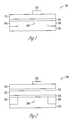
- FIG. 1The structure of a typical FET 100 is shown in FIG. 1 , where a lightly doped substrate 102 has a heavily oppositely doped source region 104 and drain region 106 .
- the portion of the substrate 102 located between the source region 104 and the drain region 106is known as the channel region 108 , and may have a doping level that is different from the doping level of the substrate 102 , and may even be counter doped to have a doping type opposite of the substrate.
- the substratemay be either lightly doped P type or N type, and the diffused source and drain regions will be heavily doped with the opposite doping type.
- gate oxide 110located over the channel region 108 , and making at least some contact with each of the source region 104 and drain region 106 .
- the gate oxide 110is an insulator, such as thermally grown silicon dioxide, and at normal operating voltages prevents current flow from the substrate 102 to a conductive gate electrode 112 .
- Conductive gate electrode 112is located on top of the gate oxide 110 , and also extends at least some distance over each of the source region 104 and drain region 106 .
- Conventional gate electrodesare formed of doped polycrystalline silicon (poly or polysilicon).
- Embodiments of the present subject matterform gate electrode 112 with a germanium silicon carbide (GeSiC) composition.
- the signal voltageaffects the concentration of electrical carriers in the channel region 108 .
- a positive voltage having a greater value than what is known as the threshold voltage of the transistor 100is applied to gate 112 , then the relatively small number of electrons (negative carriers) in the P type substrate 102 will be attracted to the channel region 108 in great enough numbers to overwhelm the positive holes in the channel region, and thus temporarily convert the channel region to be N type as long as the positive voltage is applied to the gate 112 .
- a large enough positive voltage (known as the threshold voltage) on the gate 112will electrically connect the source region 104 to the drain region 106 and turn on the transistor 100 .
- the threshold voltagedepends upon the thickness and dielectric constant of the gate insulator 110 , the doping level of the channel region 108 , and the electron affinity of the material forming the gate electrode 112 .
- a gate electrode made of a material such as GeSiCmay have the threshold voltage of the transistor adjusted to a desired level by changing the electron affinity of the transistor, and may thus reduce the number and size of ion implantation adjustments of the channel doping level.
- the illustrative floating gate transistor 200may have a lightly doped substrate 202 with a heavily oppositely doped source region 204 and drain region 206 .
- the substrate 202may be a lightly doped P type region, and the source region 204 and drain region 206 would then be heavily doped N+ type.
- the portion of the substrate 202 located between the source region 204 and the drain region 206is again known as the channel region 208 , and may have a doping level that is different from the doping level of the substrate 202 .
- There is a gate oxide 210 located over the channel region 208which is an insulator such as thermally grown silicon dioxide.
- an electrically floating conductive gate 212located on top of the gate oxide 210 , which unlike the previously discussed transistor 100 of FIG. 1 , has no direct connection to signal voltages, and is typically called a floating gate since it is electrically floating.
- floating gatesare typically formed of doped polysilicon.
- Embodiments of the present subject matterform floating gate 212 with a germanium silicon carbide composition.
- inter-gate dielectric or insulator 214which electrically separates the floating gate 212 from a control gate 216 , which is also typically made of polysilicon. In operation the control gate is connected to signal voltage 220 .
- the signal voltage 220must be larger than the signal voltage 120 for the conventional transistor since the control gate is further from the channel region 208 and because the electrons in the channel region must be at a high enough voltage to be injected through the gate oxide 210 to become trapped on floating gate 212 .
- a given signal voltage levelwill provide a current of electrons through the gate oxide 210 that depends exponentially upon the level of the signal voltage, the thickness of the gate oxide 206 and the electrical height of the barrier formed by the gate oxide 210 between the energy levels of the substrate at the channel 208 and the energy level of the floating gate 212 .
- Changing the material of the substrate 202 or of the floating gate 212changes the electrical height of the barrier formed by the gate oxide 210 , and radically changes the amount of current that tunnels through the gate oxide 206 by means of Fowler-Nordheim tunneling.
- changing the tunneling barrier heightresults in erase operations that have larger currents at a given erase voltage level, and therefore result in faster erase times for memory devices.
- Another advantage of lowering the tunneling barrier heightis that lower erase voltages may be used. Lower erase voltages mean lower electrical fields for a given dielectric thickness, and therefore reduced reliability issues such as time dependent dielectric breakdown of the gate insulator and inter-gate insulator.
- the interface between the two insulatorsmay have large numbers of what are known as trap states, and may have band gap discontinuities and differences in the conductivity of the insulator films.
- changing the gate insulator to reduce the tunneling barrier height and voltagemay pose problems, particularly with maintaining consistent time-dependent device electrical operation.
- Another method of changing the tunneling voltage, and thus equivalently increasing the tunneling current at a particular voltage level,is to change the overall tunneling barrier height by increasing the internal energy level of the conductors on either side of the insulator, rather than by lowering the insulator barrier level.
- Changing the silicon substrate to some other materialmay cause numerous practical problems in the fabrication of devices, since so much is known about the use of silicon.
- Changing the material of the floating gate to a material with what is known as a lower electron affinity, denoted by the lower case Greek letter Chi ( ⁇ )results in higher tunneling currents.
- a lower electron affinityreduces the effective height of the insulator tunneling barrier, which as noted previously has an exponential effect on the amount of tunneling current at a given voltage.
- a transistor built on a single crystal silicon substratehas a band gap diagram 300 , with a conduction level 302 , a valence level 304 , and a Fermi level 306 , as shown for a lightly doped P type silicon substrate with reference to the vacuum level 308 , which represents the amount of energy it would take to remove an electron from the silicon.
- a gate oxide 309heavily doped N type polycrystalline silicon will have a conduction level 310 , a Fermi level 312 and a valence level 314 .
- the gate oxide 309has an energy level value 316 , whose difference from the vacuum level 308 represents the electron affinity ⁇ of the gate oxide, typically thermally grown silicon dioxide.
- the value of ⁇is 0.9 eV.
- the value of electron affinity ⁇is the difference between 310 and the vacuum level 308 , and for doped polysilicon is approximately 4.1 eV.
- the barrier that an electron tunneling from the floating gate 212 conduction band 310 to the silicon substrate 202 in the area of the channel 208 , must traverse during an erase operationis the height represented by the difference between the top of the gate oxide 316 and the conduction band 310 , or 4.1 eV minus 0.9 eV, or about 3.2 eV.
- the tunneling rateis an exponential factor of the height of the barrier, and the width of the oxide, which is controlled by the process parameter of gate oxide thickness.
- the distance between the conduction level 310 and the valence level 314is known as the band gap, and has a value in silicon of approximately 1.1 eV. Since the value of electron affinity for the gate oxide is not going to change, then the use of a floating gate material that has a larger band gap would result in a lower electron affinity, and thus a reduced tunneling barrier. Changing the electron affinity of the gate material also changes the threshold voltage of the transistor, and may be used in conjunction with channel doping levels and gate insulator thickness and dielectric constant to adjust the threshold voltage level.
- FIG. 4illustrates the band gap diagram 400 for an embodiment of a silicon carbide gate material.
- a silicon substrate conduction level 402There is still a silicon substrate conduction level 402 , a silicon substrate valence level 404 , and a Fermi level 406 with reference to the vacuum level 408 .
- the illustrative silicon carbide gatewill have a conduction level 410 , a Fermi level 412 and a valence level 414 , all of which may be different from the values in the case of polysilicon gates.
- the gate oxide 409still has the same energy value 416 , and electron affinity ⁇ of the gate oxide, typically 0.9 eV.
- the band gap for silicon carbidedepends upon the ratio of silicon to carbon, and varies from the silicon value of 1.1, as noted above, to the pure carbon value of approximately 4.2 eV.
- the value of the band gapis about 2.1 eV to 2.6 eV depending upon the percentage of carbon. Since the conduction band is now closer to the vacuum level 408 , the electron affinity is lower, about 3.7 eV, and the height of the tunneling barrier is now lower, typically below 2.8 eV, which is lower than the tunneling barrier found in the case of polysilicon of about 3.2 eV. Thus, the tunneling barrier is lowered, and even a small difference in tunneling barrier height causes a large change in tunneling current.
- a very similar band diagramshows a tunneling barrier that extends from a larger value than that of polysilicon for a pure germanium gate of 3.6 eV, to a barrier value that is the same as the polysilicon value of 3.2 eV at a 4% carbon content, to lower values for increased carbon content above the 4% level.
- the values for silicon, silicon carbide and germanium carbideare discussed in more detail with respect to FIG. 5 later in this disclosure.
- Increased tunneling current flow at a given erase voltage valueresults in much faster erase operations and improved EEPROM or flash memory operational speeds.
- Crystalline silicon carbide and silicon germanium carbidecan be epitaxially grown on a silicon substrate and may be used in both metal oxide semiconductor field effect transistors (MOSFET) or bipolar transistor devices, with the silicon substrate acting as a seed layer for crystal growth.
- MOSFETmetal oxide semiconductor field effect transistor
- the silicon carbide, germanium carbide and silicon germanium carbideare microcrystalline or amorphous.
- Such microcrystalline layers or amorphous layersmay be grown on insulator layers such as silicon dioxide gate insulator layers, or other insulator layers, by chemical vapor deposition (CVD), laser assisted CVD, plasma CVD, ultra-high vacuum CVD, or sputtering.
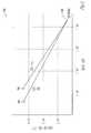
- FIG. 5is a graph 500 that illustrates the ability to adjust the tunneling barrier height, and thus the tunneling barrier current level, for various embodiments of mixtures of silicon 504 , germanium 506 , and carbon in the form of diamond 508 .
- the values of germanium carbide of varying percentages of germaniumare shown by the line connecting 506 and 508 , including the interesting point 510 where a 4% carbon value in germanium provides the same band gap 1.1 eV as pure silicon 504 , but with a lower electron affinity ⁇ and thus improved tunneling currents and faster erase operations without other significant electrical changes in the transistor operation due to changes in the band gap value.
- Silicon carbide valuesare projected on the line from 504 to 508 , with silicon carbide having a band gap with a 2.1 eV value shown at 512 .
- Various embodiments of the present disclosed methods and devicescan be found in the region of the graph between 510 and 512 and the entire area between the lines representing germanium carbide and silicon carbide compositions.
- An illustrative silicon germanium carbide material with equal amounts of silicon and germanium and varying amounts of carbonwould have a band gap to electron affinity ⁇ curve that fits about halfway between the germanium carbide line and the silicon carbide line.
- FIG. 6depicts a diagram of an embodiment of a system 600 having a controller 602 and a memory 606 .
- Controller 602 and/or memory 606include a transistor having a gate electrode made of a mixture of germanium, silicon and carbon.
- System 600also includes an electronic apparatus 608 , and a bus 604 , where bus 604 may provide electrical conductivity and data transmission between controller 602 and electronic apparatus 608 , and between controller 602 and memory 606 .
- Bus 604may include an address, a data bus, and a control bus, each independently configured.
- Bus 604also uses common conductive lines for providing address, data, and/or control, the use of which may be regulated by controller 602 .
- electronic apparatus 608includes additional memory devices configured similarly to memory 606 .
- Electronic apparatus 608may include, but is not limited to, information handling devices, wireless systems, telecommunication systems, fiber optic systems, electro-optic systems, and computers.
- An embodimentincludes an additional peripheral device or devices 610 coupled to bus 604 .
- controller 602is a processor. Any of controller 602 , memory 606 , bus 604 , electronic apparatus 608 , and peripheral device or devices 610 may include a gate electrode formed of a mixture of silicon, germanium and carbon in accordance with the disclosed embodiments.
- System 600may include, but is not limited to, information handling devices, telecommunication systems, and computers.
- Peripheral devices 610may include displays, additional storage memory, or other control devices that may operate in conjunction with controller 602 and/or memory 606 . It will be understood that embodiments are equally applicable to any size and type of memory circuit and are not intended to be limited to a particular type of memory device.
- An embodimenthas a floating gate transistor with a gate made of a material having a lower tunneling barrier and thus lower erase times. Another embodiment has the floating gate formed of germanium silicon carbide. Another embodiment has the composition of the floating gate determined by a desired tunneling current. Another embodiment includes a transistor with a conventional gate having the composition of the germanium silicon carbide adjusted to optimize the threshold of a metal oxide semiconductor field effect transistor (MOSFET).
- MOSFETmetal oxide semiconductor field effect transistor
- An embodiment for a method for forming a floating gate memory deviceincludes forming a floating gate having a lower tunneling barrier by forming the gate of a mixture of germanium, silicon and carbon. Another embodiment includes a method of storing data by setting the voltage of the control gate, drain diffusion and source diffusion to either trap electrons on a floating gate made of germanium, silicon and carbon, or by ejecting trapped electrons from the floating gate by Fowler-Nordheim tunneling.
- Applicationsinclude structures for transistors, memory devices such as flash, and electronic systems with gates containing a mixture of germanium, silicon and carbon, and methods for forming such structures.
Landscapes
- Non-Volatile Memory (AREA)
- Semiconductor Memories (AREA)
Abstract
Description
Claims (34)
Priority Applications (1)
| Application Number | Priority Date | Filing Date | Title |
|---|---|---|---|
| US11/731,712US7879674B2 (en) | 2005-02-23 | 2007-03-30 | Germanium-silicon-carbide floating gates in memories |
Applications Claiming Priority (2)
| Application Number | Priority Date | Filing Date | Title |
|---|---|---|---|
| US11/063,825US8330202B2 (en) | 2005-02-23 | 2005-02-23 | Germanium-silicon-carbide floating gates in memories |
| US11/731,712US7879674B2 (en) | 2005-02-23 | 2007-03-30 | Germanium-silicon-carbide floating gates in memories |
Related Parent Applications (1)
| Application Number | Title | Priority Date | Filing Date |
|---|---|---|---|
| US11/063,825DivisionUS8330202B2 (en) | 2005-02-23 | 2005-02-23 | Germanium-silicon-carbide floating gates in memories |
Publications (2)
| Publication Number | Publication Date |
|---|---|
| US20070170492A1 US20070170492A1 (en) | 2007-07-26 |
| US7879674B2true US7879674B2 (en) | 2011-02-01 |
Family
ID=36911770
Family Applications (3)
| Application Number | Title | Priority Date | Filing Date |
|---|---|---|---|
| US11/063,825Active2029-05-19US8330202B2 (en) | 2005-02-23 | 2005-02-23 | Germanium-silicon-carbide floating gates in memories |
| US11/731,712Active2026-03-24US7879674B2 (en) | 2005-02-23 | 2007-03-30 | Germanium-silicon-carbide floating gates in memories |
| US11/731,255AbandonedUS20070195608A1 (en) | 2005-02-23 | 2007-03-30 | Germanium-silicon-carbide floating gates in memories |
Family Applications Before (1)
| Application Number | Title | Priority Date | Filing Date |
|---|---|---|---|
| US11/063,825Active2029-05-19US8330202B2 (en) | 2005-02-23 | 2005-02-23 | Germanium-silicon-carbide floating gates in memories |
Family Applications After (1)
| Application Number | Title | Priority Date | Filing Date |
|---|---|---|---|
| US11/731,255AbandonedUS20070195608A1 (en) | 2005-02-23 | 2007-03-30 | Germanium-silicon-carbide floating gates in memories |
Country Status (1)
| Country | Link |
|---|---|
| US (3) | US8330202B2 (en) |
Cited By (1)
| Publication number | Priority date | Publication date | Assignee | Title |
|---|---|---|---|---|
| US8759900B2 (en) | 2012-03-30 | 2014-06-24 | Samsung Electronics Co., Ltd. | Semiconductor memory devices |
Families Citing this family (36)
| Publication number | Priority date | Publication date | Assignee | Title |
|---|---|---|---|---|
| US7476925B2 (en) | 2001-08-30 | 2009-01-13 | Micron Technology, Inc. | Atomic layer deposition of metal oxide and/or low asymmetrical tunnel barrier interploy insulators |
| US7068544B2 (en) | 2001-08-30 | 2006-06-27 | Micron Technology, Inc. | Flash memory with low tunnel barrier interpoly insulators |
| US6778441B2 (en)* | 2001-08-30 | 2004-08-17 | Micron Technology, Inc. | Integrated circuit memory device and method |
| US6963103B2 (en) | 2001-08-30 | 2005-11-08 | Micron Technology, Inc. | SRAM cells with repressed floating gate memory, low tunnel barrier interpoly insulators |
| US7132711B2 (en)* | 2001-08-30 | 2006-11-07 | Micron Technology, Inc. | Programmable array logic or memory with p-channel devices and asymmetrical tunnel barriers |
| US7087954B2 (en) | 2001-08-30 | 2006-08-08 | Micron Technology, Inc. | In service programmable logic arrays with low tunnel barrier interpoly insulators |
| US6888739B2 (en)* | 2002-06-21 | 2005-05-03 | Micron Technology Inc. | Nanocrystal write once read only memory for archival storage |
| US7235501B2 (en) | 2004-12-13 | 2007-06-26 | Micron Technology, Inc. | Lanthanum hafnium oxide dielectrics |
| US7560395B2 (en) | 2005-01-05 | 2009-07-14 | Micron Technology, Inc. | Atomic layer deposited hafnium tantalum oxide dielectrics |
| US8330202B2 (en)* | 2005-02-23 | 2012-12-11 | Micron Technology, Inc. | Germanium-silicon-carbide floating gates in memories |
| US7662729B2 (en) | 2005-04-28 | 2010-02-16 | Micron Technology, Inc. | Atomic layer deposition of a ruthenium layer to a lanthanide oxide dielectric layer |
| US7927948B2 (en) | 2005-07-20 | 2011-04-19 | Micron Technology, Inc. | Devices with nanocrystals and methods of formation |
| US7410910B2 (en) | 2005-08-31 | 2008-08-12 | Micron Technology, Inc. | Lanthanum aluminum oxynitride dielectric films |
| US7972974B2 (en) | 2006-01-10 | 2011-07-05 | Micron Technology, Inc. | Gallium lanthanide oxide films |
| EP1818989A3 (en)* | 2006-02-10 | 2010-12-01 | Semiconductor Energy Laboratory Co., Ltd. | Nonvolatile semiconductor storage device and manufacturing method thereof |
| US7709402B2 (en) | 2006-02-16 | 2010-05-04 | Micron Technology, Inc. | Conductive layers for hafnium silicon oxynitride films |
| EP1837917A1 (en)* | 2006-03-21 | 2007-09-26 | Semiconductor Energy Laboratory Co., Ltd. | Nonvolatile semiconductor memory device |
| EP1837900A3 (en)* | 2006-03-21 | 2008-10-15 | Semiconductor Energy Laboratory Co., Ltd. | Nonvolatile semiconductor memory device |
| TWI416738B (en)* | 2006-03-21 | 2013-11-21 | Semiconductor Energy Lab | Nonvolatile semiconductor memory device |
| KR101488516B1 (en)* | 2006-03-21 | 2015-02-02 | 가부시키가이샤 한도오따이 에네루기 켄큐쇼 | Nonvolatile semiconductor memory device |
| US7786526B2 (en)* | 2006-03-31 | 2010-08-31 | Semiconductor Energy Laboratory Co., Ltd. | Nonvolatile semiconductor memory device |
| EP1840947A3 (en)* | 2006-03-31 | 2008-08-13 | Semiconductor Energy Laboratory Co., Ltd. | Nonvolatile semiconductor memory device |
| US7554854B2 (en)* | 2006-03-31 | 2009-06-30 | Semiconductor Energy Laboratory Co., Ltd. | Method for deleting data from NAND type nonvolatile memory |
| US8022460B2 (en)* | 2006-03-31 | 2011-09-20 | Semiconductor Energy Laboratory Co., Ltd. | Nonvolatile semiconductor memory device |
| US7727908B2 (en) | 2006-08-03 | 2010-06-01 | Micron Technology, Inc. | Deposition of ZrA1ON films |
| US7563730B2 (en) | 2006-08-31 | 2009-07-21 | Micron Technology, Inc. | Hafnium lanthanide oxynitride films |
| US7605030B2 (en) | 2006-08-31 | 2009-10-20 | Micron Technology, Inc. | Hafnium tantalum oxynitride high-k dielectric and metal gates |
| US7759747B2 (en) | 2006-08-31 | 2010-07-20 | Micron Technology, Inc. | Tantalum aluminum oxynitride high-κ dielectric |
| US7432548B2 (en) | 2006-08-31 | 2008-10-07 | Micron Technology, Inc. | Silicon lanthanide oxynitride films |
| US7776765B2 (en) | 2006-08-31 | 2010-08-17 | Micron Technology, Inc. | Tantalum silicon oxynitride high-k dielectrics and metal gates |
| US7544604B2 (en) | 2006-08-31 | 2009-06-09 | Micron Technology, Inc. | Tantalum lanthanide oxynitride films |
| WO2011065243A1 (en) | 2009-11-28 | 2011-06-03 | Semiconductor Energy Laboratory Co., Ltd. | Semiconductor device and manufacturing method thereof |
| US9364302B2 (en) | 2012-02-08 | 2016-06-14 | Global Dental Science Llc | Process and systems for molding thermosetting plastics |
| WO2014120807A1 (en)* | 2013-01-29 | 2014-08-07 | The Trustees Of Boston College | High thermal conductivity materials for thermal management applications |
| CN107546299B (en)* | 2016-06-28 | 2019-05-10 | 西安电子科技大学 | Direct bandgap modified Ge material based on selective epitaxy of GeSiC and preparation method thereof |
| US20190279981A1 (en)* | 2018-03-06 | 2019-09-12 | International Business Machines Corporation | Vertical transport complimentary metal-oxide-semiconductor with varying threshold voltages |
Citations (62)
| Publication number | Priority date | Publication date | Assignee | Title |
|---|---|---|---|---|
| US3641516A (en) | 1969-09-15 | 1972-02-08 | Ibm | Write once read only store semiconductor memory |
| US3665423A (en) | 1969-03-15 | 1972-05-23 | Nippon Electric Co | Memory matrix using mis semiconductor element |
| US4507673A (en) | 1979-10-13 | 1985-03-26 | Tokyo Shibaura Denki Kabushiki Kaisha | Semiconductor memory device |
| US4597159A (en)* | 1984-03-09 | 1986-07-01 | Kabushiki Kaisha Toshiba | Method of manufacturing SiO2 -Si interface for floating gate semiconductor device |
| US4939559A (en) | 1981-12-14 | 1990-07-03 | International Business Machines Corporation | Dual electron injector structures using a conductive oxide between injectors |
| US5021999A (en) | 1987-12-17 | 1991-06-04 | Mitsubishi Denki Kabushiki Kaisha | Non-volatile semiconductor memory device with facility of storing tri-level data |
| US5032533A (en)* | 1989-12-04 | 1991-07-16 | Texas Instruments Incorporated | Method of making a nonvolatile memory cell with field-plate switch |
| JPH03222367A (en) | 1990-01-26 | 1991-10-01 | Fujitsu Ltd | Insulated gate type field effect transistor |
| US5057446A (en)* | 1990-08-06 | 1991-10-15 | Texas Instruments Incorporated | Method of making an EEPROM with improved capacitive coupling between control gate and floating gate |
| US5111430A (en) | 1989-06-22 | 1992-05-05 | Nippon Telegraph And Telephone Corporation | Non-volatile memory with hot carriers transmitted to floating gate through control gate |
| US5298447A (en) | 1993-07-22 | 1994-03-29 | United Microelectronics Corporation | Method of fabricating a flash memory cell |
| JPH06224431A (en) | 1993-01-26 | 1994-08-12 | Sharp Corp | Thin-film transistor and liquid crystal display panel |
| JPH06302828A (en) | 1993-04-14 | 1994-10-28 | Matsushita Electric Ind Co Ltd | Nonvolatile semiconductor memory device |
| US5457649A (en) | 1994-08-26 | 1995-10-10 | Microchip Technology, Inc. | Semiconductor memory device and write-once, read-only semiconductor memory array using amorphous-silicon and method therefor |
| US5493140A (en) | 1993-07-05 | 1996-02-20 | Sharp Kabushiki Kaisha | Nonvolatile memory cell and method of producing the same |
| JPH08255878A (en) | 1995-03-16 | 1996-10-01 | Fujitsu Ltd | Floating gate transistor and manufacturing method thereof |
| US5670790A (en) | 1995-09-21 | 1997-09-23 | Kabushikik Kaisha Toshiba | Electronic device |
| US5714766A (en) | 1995-09-29 | 1998-02-03 | International Business Machines Corporation | Nano-structure memory device |
| US5740104A (en) | 1997-01-29 | 1998-04-14 | Micron Technology, Inc. | Multi-state flash memory cell and method for programming single electron differences |
| US5768192A (en) | 1996-07-23 | 1998-06-16 | Saifun Semiconductors, Ltd. | Non-volatile semiconductor memory cell utilizing asymmetrical charge trapping |
| US5801401A (en) | 1997-01-29 | 1998-09-01 | Micron Technology, Inc. | Flash memory with microcrystalline silicon carbide film floating gate |
| US5852306A (en) | 1997-01-29 | 1998-12-22 | Micron Technology, Inc. | Flash memory with nanocrystalline silicon film floating gate |
| US5888867A (en)* | 1998-02-13 | 1999-03-30 | Advanced Micro Devices, Inc. | Non-uniform threshold voltage adjustment in flash eproms through gate work function alteration |
| US5973355A (en) | 1996-05-24 | 1999-10-26 | Nec Corporation | Nonvolatile semiconductor memory device and manufacturing method of the same |
| US6125062A (en) | 1998-08-26 | 2000-09-26 | Micron Technology, Inc. | Single electron MOSFET memory device and method |
| US6141260A (en) | 1998-08-27 | 2000-10-31 | Micron Technology, Inc. | Single electron resistor memory device and method for use thereof |
| US6246606B1 (en) | 1997-11-13 | 2001-06-12 | Micron Technology, Inc. | Memory using insulator traps |
| US6313518B1 (en) | 1997-10-14 | 2001-11-06 | Micron Technology, Inc. | Porous silicon oxycarbide integrated circuit insulator |
| US20020003252A1 (en) | 1998-09-03 | 2002-01-10 | Ravi Iyer | Flash memory circuit with with resistance to disturb effect |
| US6404681B1 (en) | 2000-02-02 | 2002-06-11 | Sharp Kabushiki Kaisha | Method for erasing data from a non-volatile semiconductor memory device |
| US20020109158A1 (en) | 2001-02-09 | 2002-08-15 | Leonard Forbes | Dynamic memory based on single electron storage |
| US20020110983A1 (en) | 2001-02-09 | 2002-08-15 | Chih-Cheng Liu | Method of fabricating a split-gate flash memory cell |
| US20020110973A1 (en) | 2001-02-13 | 2002-08-15 | United Microelectronics Corp. | Fabrication method and structure of a flash memory |
| US20020109138A1 (en) | 2001-02-09 | 2002-08-15 | Micron Technology, Inc. | Programmable memory address and decode circuits with ultra thin vertical body transistors |
| US6476434B1 (en) | 1997-07-08 | 2002-11-05 | Micron Tecnology, Inc. | 4 F2 folded bit line dram cell structure having buried bit and word lines |
| US20020176293A1 (en) | 1999-02-26 | 2002-11-28 | Micron Technology, Inc. | DRAM technology compatible processor/memory chips |
| US6504207B1 (en) | 2000-06-30 | 2003-01-07 | International Business Machines Corporation | Method to create EEPROM memory structures integrated with high performance logic and NVRAM, and operating conditions for the same |
| US20030042528A1 (en) | 2001-08-30 | 2003-03-06 | Leonard Forbes | Sram cells with repressed floating gate memory, low tunnel barrier interpoly insulators |
| US20030043637A1 (en) | 2001-08-30 | 2003-03-06 | Micron Technology, Inc | Flash memory with low tunnel barrier interpoly insulators |
| US20030049900A1 (en) | 2001-08-30 | 2003-03-13 | Micron Technology Inc. | Graded composition gate insulators to reduce tunneling barriers in flash memory devices |
| US20030048666A1 (en) | 2001-08-30 | 2003-03-13 | Micron Technology, Inc. | Graded composition metal oxide tunnel barrier interpoly insulators |
| US6574143B2 (en) | 1999-12-09 | 2003-06-03 | Hitachi Europe, Ltd. | Memory device using hot charge carrier converters |
| US6580124B1 (en) | 2000-08-14 | 2003-06-17 | Matrix Semiconductor Inc. | Multigate semiconductor device with vertical channel current and method of fabrication |
| US20030207032A1 (en) | 2002-05-02 | 2003-11-06 | Micron Technology, Inc. | Methods, systems, and apparatus for atomic-layer deposition of aluminum oxides in integrated circuits |
| US20030207540A1 (en) | 2002-05-02 | 2003-11-06 | Micron Technology, Inc. | Atomic layer-deposited laaio3 films for gate dielectrics |
| US6710465B2 (en) | 2001-06-21 | 2004-03-23 | Samsung Electronics Co., Ltd. | Scalable two transistor memory device |
| US6717340B2 (en) | 2001-09-26 | 2004-04-06 | Canon Kabushiki Kaisha | Electron-emitting device and image-forming apparatus |
| US6723606B2 (en) | 2000-06-29 | 2004-04-20 | California Institute Of Technology | Aerosol process for fabricating discontinuous floating gate microelectronic devices |
| US6753568B1 (en) | 1996-11-15 | 2004-06-22 | Hitachi, Ltd. | Memory device |
| US20040160830A1 (en) | 2001-08-30 | 2004-08-19 | Micron Technology, Inc. | DRAM cells with repressed floating gate memory, low tunnel barrier interpoly insulators |
| US6794255B1 (en) | 1997-07-29 | 2004-09-21 | Micron Technology, Inc. | Carburized silicon gate insulators for integrated circuits |
| US20050024945A1 (en) | 2001-08-30 | 2005-02-03 | Micron Technology, Inc. | Programmable memory address and decode circuits with low tunnel barrier interpoly insulators |
| US20050023595A1 (en) | 2001-08-30 | 2005-02-03 | Micron Technology, Inc. | Programmable array logic or memory devices with asymmetrical tunnel barriers |
| US20050023603A1 (en) | 2001-08-30 | 2005-02-03 | Micron Technology, Inc. | Atomic layer deposition of metal oxide and/or low asymmetrical tunnel barrier interpoly insulators |
| US20050023602A1 (en) | 2001-08-30 | 2005-02-03 | Micron Technology, Inc. | Programmable array logic or memory with p-channel devices and asymmetrical tunnel barriers |
| US6888739B2 (en) | 2002-06-21 | 2005-05-03 | Micron Technology Inc. | Nanocrystal write once read only memory for archival storage |
| US6950340B2 (en) | 2002-02-12 | 2005-09-27 | Micron Technology, Inc. | Asymmetric band-gap engineered nonvolatile memory device |
| US20060001049A1 (en) | 2001-08-30 | 2006-01-05 | Micron Technology, Inc. | Service programmable logic arrays with low tunnel barrier interpoly insulators |
| US20060002192A1 (en) | 2001-08-30 | 2006-01-05 | Micron Technology | Integrated circuit memory device and method |
| US20060170029A1 (en)* | 2005-01-28 | 2006-08-03 | Taiwan Semiconductor Manufacturing Company, Ltd. | Novel process for erase improvement in a non-volatile memory device |
| US7133316B2 (en) | 2004-06-02 | 2006-11-07 | Macronix International Co., Ltd. | Program/erase method for P-channel charge trapping memory device |
| US20070195608A1 (en) | 2005-02-23 | 2007-08-23 | Micron Technology, Inc. | Germanium-silicon-carbide floating gates in memories |
Family Cites Families (14)
| Publication number | Priority date | Publication date | Assignee | Title |
|---|---|---|---|---|
| US5751038A (en) | 1996-11-26 | 1998-05-12 | Philips Electronics North America Corporation | Electrically erasable and programmable read only memory (EEPROM) having multiple overlapping metallization layers |
| US6124608A (en) | 1997-12-18 | 2000-09-26 | Advanced Micro Devices, Inc. | Non-volatile trench semiconductor device having a shallow drain region |
| US6093606A (en) | 1998-03-05 | 2000-07-25 | Taiwan Semiconductor Manufacturing Company | Method of manufacture of vertical stacked gate flash memory device |
| US6147378A (en) | 1998-03-30 | 2000-11-14 | Advanced Micro Devices, Inc. | Fully recessed semiconductor device and method for low power applications with single wrap around buried drain region |
| US6118147A (en) | 1998-07-07 | 2000-09-12 | Advanced Micro Devices, Inc. | Double density non-volatile memory cells |
| US6180461B1 (en) | 1998-08-03 | 2001-01-30 | Halo Lsi Design & Device Technology, Inc. | Double sidewall short channel split gate flash memory |
| US6130453A (en) | 1999-01-04 | 2000-10-10 | International Business Machines Corporation | Flash memory structure with floating gate in vertical trench |
| TW419822B (en) | 1999-07-12 | 2001-01-21 | Mosel Vitelic Inc | Trench type non-volatile memory cell and its manufacturing method |
| US6262917B1 (en) | 1999-10-22 | 2001-07-17 | United Microelectronics Corp. | Structure of a flash memory device |
| KR100442090B1 (en) | 2002-03-28 | 2004-07-27 | 삼성전자주식회사 | Non-volatile memory cells having a split gate structure and methods of fabricating the same |
| TW533551B (en) | 2002-05-01 | 2003-05-21 | Nanya Technology Corp | Vertical split gate flash memory and its formation method |
| US7153744B2 (en) | 2003-12-03 | 2006-12-26 | Taiwan Semiconductor Manufacturing Company, Ltd. | Method of forming self-aligned poly for embedded flash |
| US7163863B2 (en) | 2004-06-29 | 2007-01-16 | Skymedi Corporation | Vertical memory cell and manufacturing method thereof |
| US7205601B2 (en) | 2005-06-09 | 2007-04-17 | Taiwan Semiconductor Manufacturing Company, Ltd. | FinFET split gate EEPROM structure and method of its fabrication |
- 2005
- 2005-02-23USUS11/063,825patent/US8330202B2/enactiveActive
- 2007
- 2007-03-30USUS11/731,712patent/US7879674B2/enactiveActive
- 2007-03-30USUS11/731,255patent/US20070195608A1/ennot_activeAbandoned
Patent Citations (101)
| Publication number | Priority date | Publication date | Assignee | Title |
|---|---|---|---|---|
| US3665423A (en) | 1969-03-15 | 1972-05-23 | Nippon Electric Co | Memory matrix using mis semiconductor element |
| US3641516A (en) | 1969-09-15 | 1972-02-08 | Ibm | Write once read only store semiconductor memory |
| US4507673A (en) | 1979-10-13 | 1985-03-26 | Tokyo Shibaura Denki Kabushiki Kaisha | Semiconductor memory device |
| US4939559A (en) | 1981-12-14 | 1990-07-03 | International Business Machines Corporation | Dual electron injector structures using a conductive oxide between injectors |
| US4597159A (en)* | 1984-03-09 | 1986-07-01 | Kabushiki Kaisha Toshiba | Method of manufacturing SiO2 -Si interface for floating gate semiconductor device |
| US5021999A (en) | 1987-12-17 | 1991-06-04 | Mitsubishi Denki Kabushiki Kaisha | Non-volatile semiconductor memory device with facility of storing tri-level data |
| US5111430A (en) | 1989-06-22 | 1992-05-05 | Nippon Telegraph And Telephone Corporation | Non-volatile memory with hot carriers transmitted to floating gate through control gate |
| US5032533A (en)* | 1989-12-04 | 1991-07-16 | Texas Instruments Incorporated | Method of making a nonvolatile memory cell with field-plate switch |
| JPH03222367A (en) | 1990-01-26 | 1991-10-01 | Fujitsu Ltd | Insulated gate type field effect transistor |
| US5057446A (en)* | 1990-08-06 | 1991-10-15 | Texas Instruments Incorporated | Method of making an EEPROM with improved capacitive coupling between control gate and floating gate |
| JPH06224431A (en) | 1993-01-26 | 1994-08-12 | Sharp Corp | Thin-film transistor and liquid crystal display panel |
| JPH06302828A (en) | 1993-04-14 | 1994-10-28 | Matsushita Electric Ind Co Ltd | Nonvolatile semiconductor memory device |
| US5493140A (en) | 1993-07-05 | 1996-02-20 | Sharp Kabushiki Kaisha | Nonvolatile memory cell and method of producing the same |
| US5298447A (en) | 1993-07-22 | 1994-03-29 | United Microelectronics Corporation | Method of fabricating a flash memory cell |
| US5457649A (en) | 1994-08-26 | 1995-10-10 | Microchip Technology, Inc. | Semiconductor memory device and write-once, read-only semiconductor memory array using amorphous-silicon and method therefor |
| JPH08255878A (en) | 1995-03-16 | 1996-10-01 | Fujitsu Ltd | Floating gate transistor and manufacturing method thereof |
| US5670790A (en) | 1995-09-21 | 1997-09-23 | Kabushikik Kaisha Toshiba | Electronic device |
| US5714766A (en) | 1995-09-29 | 1998-02-03 | International Business Machines Corporation | Nano-structure memory device |
| US5973355A (en) | 1996-05-24 | 1999-10-26 | Nec Corporation | Nonvolatile semiconductor memory device and manufacturing method of the same |
| US5768192A (en) | 1996-07-23 | 1998-06-16 | Saifun Semiconductors, Ltd. | Non-volatile semiconductor memory cell utilizing asymmetrical charge trapping |
| US6753568B1 (en) | 1996-11-15 | 2004-06-22 | Hitachi, Ltd. | Memory device |
| US5989958A (en) | 1997-01-29 | 1999-11-23 | Micron Technology, Inc. | Flash memory with microcrystalline silicon carbide film floating gate |
| US5852306A (en) | 1997-01-29 | 1998-12-22 | Micron Technology, Inc. | Flash memory with nanocrystalline silicon film floating gate |
| US5740104A (en) | 1997-01-29 | 1998-04-14 | Micron Technology, Inc. | Multi-state flash memory cell and method for programming single electron differences |
| US5801401A (en) | 1997-01-29 | 1998-09-01 | Micron Technology, Inc. | Flash memory with microcrystalline silicon carbide film floating gate |
| US6166401A (en) | 1997-01-29 | 2000-12-26 | Micron Technology, Inc. | Flash memory with microcrystalline silicon carbide film floating gate |
| US6476434B1 (en) | 1997-07-08 | 2002-11-05 | Micron Tecnology, Inc. | 4 F2 folded bit line dram cell structure having buried bit and word lines |
| US6794255B1 (en) | 1997-07-29 | 2004-09-21 | Micron Technology, Inc. | Carburized silicon gate insulators for integrated circuits |
| US6313518B1 (en) | 1997-10-14 | 2001-11-06 | Micron Technology, Inc. | Porous silicon oxycarbide integrated circuit insulator |
| US6246606B1 (en) | 1997-11-13 | 2001-06-12 | Micron Technology, Inc. | Memory using insulator traps |
| US6351411B2 (en) | 1997-11-13 | 2002-02-26 | Micron Technology, Inc. | Memory using insulator traps |
| US6545314B2 (en) | 1997-11-13 | 2003-04-08 | Micron Technology, Inc. | Memory using insulator traps |
| US5888867A (en)* | 1998-02-13 | 1999-03-30 | Advanced Micro Devices, Inc. | Non-uniform threshold voltage adjustment in flash eproms through gate work function alteration |
| US6125062A (en) | 1998-08-26 | 2000-09-26 | Micron Technology, Inc. | Single electron MOSFET memory device and method |
| US6141260A (en) | 1998-08-27 | 2000-10-31 | Micron Technology, Inc. | Single electron resistor memory device and method for use thereof |
| US20020003252A1 (en) | 1998-09-03 | 2002-01-10 | Ravi Iyer | Flash memory circuit with with resistance to disturb effect |
| US20020176293A1 (en) | 1999-02-26 | 2002-11-28 | Micron Technology, Inc. | DRAM technology compatible processor/memory chips |
| US6574143B2 (en) | 1999-12-09 | 2003-06-03 | Hitachi Europe, Ltd. | Memory device using hot charge carrier converters |
| US6404681B1 (en) | 2000-02-02 | 2002-06-11 | Sharp Kabushiki Kaisha | Method for erasing data from a non-volatile semiconductor memory device |
| US6723606B2 (en) | 2000-06-29 | 2004-04-20 | California Institute Of Technology | Aerosol process for fabricating discontinuous floating gate microelectronic devices |
| US6504207B1 (en) | 2000-06-30 | 2003-01-07 | International Business Machines Corporation | Method to create EEPROM memory structures integrated with high performance logic and NVRAM, and operating conditions for the same |
| US6580124B1 (en) | 2000-08-14 | 2003-06-17 | Matrix Semiconductor Inc. | Multigate semiconductor device with vertical channel current and method of fabrication |
| US20020109138A1 (en) | 2001-02-09 | 2002-08-15 | Micron Technology, Inc. | Programmable memory address and decode circuits with ultra thin vertical body transistors |
| US20020110983A1 (en) | 2001-02-09 | 2002-08-15 | Chih-Cheng Liu | Method of fabricating a split-gate flash memory cell |
| US6903367B2 (en) | 2001-02-09 | 2005-06-07 | Micron Technology Inc. | Programmable memory address and decode circuits with vertical body transistors |
| US20020109158A1 (en) | 2001-02-09 | 2002-08-15 | Leonard Forbes | Dynamic memory based on single electron storage |
| US6566682B2 (en) | 2001-02-09 | 2003-05-20 | Micron Technology, Inc. | Programmable memory address and decode circuits with ultra thin vertical body transistors |
| US20020110973A1 (en) | 2001-02-13 | 2002-08-15 | United Microelectronics Corp. | Fabrication method and structure of a flash memory |
| US6710465B2 (en) | 2001-06-21 | 2004-03-23 | Samsung Electronics Co., Ltd. | Scalable two transistor memory device |
| US20060199338A1 (en) | 2001-08-30 | 2006-09-07 | Micron Technology, Inc. | Atomic layer deposition of metal oxide and/or low asymmetrical tunnel barrier interpoly insulators |
| US7087954B2 (en) | 2001-08-30 | 2006-08-08 | Micron Technology, Inc. | In service programmable logic arrays with low tunnel barrier interpoly insulators |
| US7508025B2 (en) | 2001-08-30 | 2009-03-24 | Micron Technology, Inc. | Atomic layer deposition of metal oxide and/or low asymmetrical tunnel barrier interpoly insulators |
| US7504687B2 (en) | 2001-08-30 | 2009-03-17 | Micron Technology, Inc. | Atomic layer deposition of metal oxide and/or low asymmetrical tunnel barrier interpoly insulators |
| US6586797B2 (en) | 2001-08-30 | 2003-07-01 | Micron Technology, Inc. | Graded composition gate insulators to reduce tunneling barriers in flash memory devices |
| US20030048666A1 (en) | 2001-08-30 | 2003-03-13 | Micron Technology, Inc. | Graded composition metal oxide tunnel barrier interpoly insulators |
| US20040160830A1 (en) | 2001-08-30 | 2004-08-19 | Micron Technology, Inc. | DRAM cells with repressed floating gate memory, low tunnel barrier interpoly insulators |
| US20030049900A1 (en) | 2001-08-30 | 2003-03-13 | Micron Technology Inc. | Graded composition gate insulators to reduce tunneling barriers in flash memory devices |
| US20050026349A1 (en) | 2001-08-30 | 2005-02-03 | Micron Technology, Inc. | Flash memory with low tunnel barrier interpoly insulators |
| US20050024945A1 (en) | 2001-08-30 | 2005-02-03 | Micron Technology, Inc. | Programmable memory address and decode circuits with low tunnel barrier interpoly insulators |
| US20050023595A1 (en) | 2001-08-30 | 2005-02-03 | Micron Technology, Inc. | Programmable array logic or memory devices with asymmetrical tunnel barriers |
| US20050023603A1 (en) | 2001-08-30 | 2005-02-03 | Micron Technology, Inc. | Atomic layer deposition of metal oxide and/or low asymmetrical tunnel barrier interpoly insulators |
| US20050023602A1 (en) | 2001-08-30 | 2005-02-03 | Micron Technology, Inc. | Programmable array logic or memory with p-channel devices and asymmetrical tunnel barriers |
| US7476925B2 (en) | 2001-08-30 | 2009-01-13 | Micron Technology, Inc. | Atomic layer deposition of metal oxide and/or low asymmetrical tunnel barrier interploy insulators |
| US20030043637A1 (en) | 2001-08-30 | 2003-03-06 | Micron Technology, Inc | Flash memory with low tunnel barrier interpoly insulators |
| US7473956B2 (en) | 2001-08-30 | 2009-01-06 | Micron Technology, Inc. | Atomic layer deposition of metal oxide and/or low assymmetrical tunnel barrier interpoly insulators |
| US7465983B2 (en) | 2001-08-30 | 2008-12-16 | Micron Technology, Inc. | Low tunnel barrier insulators |
| US6952032B2 (en) | 2001-08-30 | 2005-10-04 | Micron Technology, Inc. | Programmable array logic or memory devices with asymmetrical tunnel barriers |
| US20060001049A1 (en) | 2001-08-30 | 2006-01-05 | Micron Technology, Inc. | Service programmable logic arrays with low tunnel barrier interpoly insulators |
| US20060002192A1 (en) | 2001-08-30 | 2006-01-05 | Micron Technology | Integrated circuit memory device and method |
| US7027328B2 (en) | 2001-08-30 | 2006-04-11 | Micron Technology, Inc. | Integrated circuit memory device and method |
| US7042043B2 (en) | 2001-08-30 | 2006-05-09 | Micron Technology, Inc. | Programmable array logic or memory devices with asymmetrical tunnel barriers |
| US7068544B2 (en) | 2001-08-30 | 2006-06-27 | Micron Technology, Inc. | Flash memory with low tunnel barrier interpoly insulators |
| US7075829B2 (en) | 2001-08-30 | 2006-07-11 | Micron Technology, Inc. | Programmable memory address and decode circuits with low tunnel barrier interpoly insulators |
| US7074673B2 (en) | 2001-08-30 | 2006-07-11 | Micron Technology, Inc. | Service programmable logic arrays with low tunnel barrier interpoly insulators |
| US7446368B2 (en) | 2001-08-30 | 2008-11-04 | Micron Technology, Inc. | Deposition of metal oxide and/or low asymmetrical tunnel barrier interpoly insulators |
| US7391072B2 (en) | 2001-08-30 | 2008-06-24 | Micron Technology, Inc. | Programmable array logic or memory with p-channel devices and asymmetrical tunnel barriers |
| US20030042528A1 (en) | 2001-08-30 | 2003-03-06 | Leonard Forbes | Sram cells with repressed floating gate memory, low tunnel barrier interpoly insulators |
| US7112841B2 (en) | 2001-08-30 | 2006-09-26 | Micron Technology, Inc. | Graded composition metal oxide tunnel barrier interpoly insulators |
| US20060234450A1 (en) | 2001-08-30 | 2006-10-19 | Micron Technology, Inc. | Programmable array logic or memory with p-channel devices and asymmetrical tunnel barriers |
| US20060231886A1 (en) | 2001-08-30 | 2006-10-19 | Micron Technology, Inc. | Programmable array logic or memory with p-channel devices and asymmetrical tunnel barriers |
| US7126183B2 (en) | 2001-08-30 | 2006-10-24 | Micron Technology, Inc. | Programmable array logic or memory with p-channel devices and asymmetrical tunnel barriers |
| US20060237768A1 (en) | 2001-08-30 | 2006-10-26 | Micron Technology, Inc. | Programmable array logic or memory with p-channel devices and asymmetrical tunnel barriers |
| US7132711B2 (en) | 2001-08-30 | 2006-11-07 | Micron Technology, Inc. | Programmable array logic or memory with p-channel devices and asymmetrical tunnel barriers |
| US7187587B2 (en) | 2001-08-30 | 2007-03-06 | Micron Technology, Inc. | Programmable memory address and decode circuits with low tunnel barrier interpoly insulators |
| US7136302B2 (en) | 2001-08-30 | 2006-11-14 | Micron Technology, Inc. | Integrated circuit memory device and method |
| US7135734B2 (en) | 2001-08-30 | 2006-11-14 | Micron Technology, Inc. | Graded composition metal oxide tunnel barrier interpoly insulators |
| US20060278917A1 (en) | 2001-08-30 | 2006-12-14 | Micron Technology, Inc. | Floating gate structures |
| US6717340B2 (en) | 2001-09-26 | 2004-04-06 | Canon Kabushiki Kaisha | Electron-emitting device and image-forming apparatus |
| US6950340B2 (en) | 2002-02-12 | 2005-09-27 | Micron Technology, Inc. | Asymmetric band-gap engineered nonvolatile memory device |
| US20030207540A1 (en) | 2002-05-02 | 2003-11-06 | Micron Technology, Inc. | Atomic layer-deposited laaio3 films for gate dielectrics |
| US20030207032A1 (en) | 2002-05-02 | 2003-11-06 | Micron Technology, Inc. | Methods, systems, and apparatus for atomic-layer deposition of aluminum oxides in integrated circuits |
| US7257022B2 (en) | 2002-06-21 | 2007-08-14 | Micron Technology, Inc. | Nanocrystal write once read only memory for archival storage |
| US20080062757A1 (en) | 2002-06-21 | 2008-03-13 | Micron Technology, Inc. | Nanocrystal write once read only memory for archival storage |
| US7154778B2 (en) | 2002-06-21 | 2006-12-26 | Micron Technology, Inc. | Nanocrystal write once read only memory for archival storage |
| US20050199947A1 (en) | 2002-06-21 | 2005-09-15 | Micron Technology, Inc. | Nanocrystal write once read only memory for archival storage |
| US6888739B2 (en) | 2002-06-21 | 2005-05-03 | Micron Technology Inc. | Nanocrystal write once read only memory for archival storage |
| US20070091661A1 (en) | 2002-06-21 | 2007-04-26 | Micron Technology, Inc. | Nanocrystal write once read only memory for archival storage |
| US7639528B2 (en) | 2002-06-21 | 2009-12-29 | Micron Technology, Inc. | Nanocrystal write once read only memory for archival storage |
| US7133316B2 (en) | 2004-06-02 | 2006-11-07 | Macronix International Co., Ltd. | Program/erase method for P-channel charge trapping memory device |
| US20060170029A1 (en)* | 2005-01-28 | 2006-08-03 | Taiwan Semiconductor Manufacturing Company, Ltd. | Novel process for erase improvement in a non-volatile memory device |
| US20070195608A1 (en) | 2005-02-23 | 2007-08-23 | Micron Technology, Inc. | Germanium-silicon-carbide floating gates in memories |
Non-Patent Citations (114)
| Title |
|---|
| Banerjee, S. , "Applications of silicon-germanium-carbon in MOS and bipolar transistors", Proceedings of the SPIE—The International Society for Optical Engineering, 3212, (1997),118-128. |
| Beensh-Marchwicka, G. , et al., "Preparation of thermosensitive magnetron sputtered thin films", Vacuum, 53(1-2), (May 1999),47-52. |
| Dalal, Vikram L., et al., "Microcrystalline Germanium Carbide—A new material for PV conversion", Presented at 2001 NCPV Program Review Meeting, (2001),348-349. |
| Herrold, J. , et al., "Growth and properties of microcrystalline germanium-carbide alloys grown using electron cyclotron resonance plasma processing", Journal of Non-Crystalline Solids (Netherlands), 270(1-3), (May 2000),255-259. |
| Herrold, J. , et al., "Growth and properties of microcrystalline germanium-carbide alloys", Amorphous and Heterogeneous Silicon Thin Films: Fundamentals to Devices—1999 Symposium, San Francisco, CA, Apr. 5-9, 1999, 16 pgs. |
| Kouvetakis, J. , et al., "Novel chemical routes to silicon-germanium-carbon materials", Applied Physics Letters, 65(23), (Dec. 5, 1994),2960-2962. |
| Lopez, E. , et al., "Laser assisted integrated processing of SiGeC films on silicon", Thin Solid Films, vol. 453-454, (Apr. 1, 2004),46-51. |
| Pavan, Paolo , et al., "Flash Memory Cells—An Overview", Proc. IEEE, 85(8), (1997),1248-1271. |
| Summonte, C. , et al., "Wide band-gap silicon-carbon alloys deposited by very high frequency plasma enhanced chemical vapor deposition", Journal of Applied Physics, 96(7), (Oct. 1, 2004),3987-3997. |
| Tyczkowski, J. , et al., "Electronic band structure of insulating hydrogenated carbon-germanium films", Journal of Applied Physics, 86(8), (Oct. 15, 1999),4412-4418. |
| U.S. Appl. No. 09/945,500 Non Final Office action mailed Dec. 24, 2002, 5 pgs. |
| U.S. Appl. No. 09/945,500 Notice of Allowance mailed Aug. 12, 2005, 2 pgs. |
| U.S. Appl. No. 09/945,500 Notice of Allowance mailed Dec. 12, 2003, 5 pgs. |
| U.S. Appl. No. 09/945,500 Notice of Allowance mailed Dec. 2, 2005, 2 pgs. |
| U.S. Appl. No. 09/945,500 Notice of Allowance mailed Mar. 29, 2005, 4 pgs. |
| U.S. Appl. No. 09/945,500 Notice of Allowance mailed May 19, 2004, 4 pgs. |
| U.S. Appl. No. 09/945,500 Response filed Mar. 24, 2003 to Final Office action mailed Dec. 24, 2002, 17 pgs. |
| U.S. Appl. No. 10/028,001 Non Final Office action mailed Feb. 14, 2003, 12 pgs. |
| U.S. Appl. No. 10/028,001 Non Final Office action mailed Nov. 2, 2004, 5 pgs. |
| U.S. Appl. No. 10/028,001 Non Final Office action mailed Oct. 12, 2005, 12 pgs. |
| U.S. Appl. No. 10/028,001 Notice of Allowance mailed Apr. 16, 2004, 4 pgs. |
| U.S. Appl. No. 10/028,001 Notice of Allowance mailed Feb. 1, 2006, 4 pgs. |
| U.S. Appl. No. 10/028,001 Notice of Allowance mailed Feb. 25, 2005, 4 pgs. |
| U.S. Appl. No. 10/028,001 Notice of Allowance mailed Jun. 2, 2006, 3 pgs. |
| U.S. Appl. No. 10/028,001 Notice of Allowance mailed Jun. 3, 2003, 3 pgs. |
| U.S. Appl. No. 10/028,001 Notice of Allowance mailed Nov. 19, 2003, 4 pgs. |
| U.S. Appl. No. 10/028,001, Response filed Feb. 2, 2005 Non Final Office Action mailed Nov. 2, 2004, 12 pgs. |
| U.S. Appl. No. 10/028,001, Response filed Jan. 12, 2006 Non Final Office Action mailed Oct. 12, 2005, 15 pgs. |
| U.S. Appl. No. 10/028,001, Response filed May 14, 2003 Non Final Office Action mailed Feb. 14, 2003, 26 pgs. |
| U.S. Appl. No. 10/081,818 Final Office action mailed Oct. 5, 2005, 13 pgs. |
| U.S. Appl. No. 10/081,818 Non Final Office action mailed Apr. 29, 2005, 13 pgs. |
| U.S. Appl. No. 10/081,818 Non Final Office action mailed Jan. 2, 2003, 11 pgs. |
| U.S. Appl. No. 10/081,818 Non Final Office action mailed Mar. 24, 2006, 14 pgs. |
| U.S. Appl. No. 10/081,818 Non Final Office action mailed Oct. 15, 2004, 6 pgs. |
| U.S. Appl. No. 10/081,818 Notice of Allowance mailed Feb. 13, 2004, 4 pgs. |
| U.S. Appl. No. 10/081,818 Notice of Allowance mailed Feb. 22, 2005, 4 pgs. |
| U.S. Appl. No. 10/081,818 Notice of Allowance mailed Mar. 8, 2007, 3 pgs. |
| U.S. Appl. No. 10/081,818 Notice of Allowance mailed Sep. 21, 2006, 2 pgs. |
| U.S. Appl. No. 10/081,818 Notice of Allowance mailed Sep. 26, 2003, 5 pgs. |
| U.S. Appl. No. 10/081,818 Response filed Apr. 2, 2003 to Non Final Office action mailed Jan. 2, 2003, 12 pgs. |
| U.S. Appl. No. 10/081,818 Response filed Aug. 24, 2006 to Non Final Office action mailed Mar. 24, 2006, 11 pgs. |
| U.S. Appl. No. 10/081,818 Response filed Jan. 14, 2005 to Non Final Office action mailed Oct. 15, 2004, 16 pgs. |
| U.S. Appl. No. 10/081,818 Response filed Jul. 29, 2005 to Non Final Office action mailed Apr. 29, 2005, 16 pgs. |
| U.S. Appl. No. 10/081,818 Response filed Mar. 3, 2006 to Final Office action mailed Oct. 5, 2005, 14 pgs. |
| U.S. Appl. No. 10/081,818, Final Office Action mailed Mar. 24, 2006, 13 pgs. |
| U.S. Appl. No. 10/081,818, Final Office Action mailed Oct. 5, 2005, 13 pgs. |
| U.S. Appl. No. 10/081,818, Non Final Office Action mailed Apr. 29, 2005, 13 pgs. |
| U.S. Appl. No. 10/081,818, Non Final Office Action mailed Oct. 15, 2004, 6 pgs. |
| U.S. Appl. No. 10/081,818, Notice of Allowance mailed Feb. 13, 2004, 4 pgs. |
| U.S. Appl. No. 10/081,818, Notice of Allowance mailed Feb. 22, 2005, 4 pgs. |
| U.S. Appl. No. 10/081,818, Notice of Allowance mailed Mar. 8, 2007, 3 pgs. |
| U.S. Appl. No. 10/081,818, Notice of Allowance mailed Oct. 30, 2007, 7 pgs. |
| U.S. Appl. No. 10/081,818, Notice of Allowance mailed Sep. 21, 2006, 2 pgs. |
| U.S. Appl. No. 10/081,818, Notice of Allowance mailed Sep. 26, 2003, 5 pgs. |
| U.S. Appl. No. 10/081,818, Response filed Apr. 2, 2003 Non Final Office Action mailed Jan. 2, 2003, 11 pgs. |
| U.S. Appl. No. 10/081,818, Response filed Aug. 24, 2006 Non Final Office Action mailed Mar. 24, 2006, 11 pgs. |
| U.S. Appl. No. 10/081,818, Response filed Jan. 14, 2005 Non Final Office Action mailed Oct. 15, 2004, 8 pgs. |
| U.S. Appl. No. 10/081,818, Response filed Jul. 29, 2005 Non Final Office Action mailed Apr. 29, 2005, 16 pgs. |
| U.S. Appl. No. 10/081,818, Response filed Mar. 3, 2006 Final Office Action mailed Oct. 5, 2005, 14 pgs. |
| U.S. Appl. No. 10/177,096 Non Final Office Action mailed Jun. 10, 2003, 10 pgs. |
| U.S. Appl. No. 10/177,096 Non Final Office Action mailed Jun. 14, 2005, 18 pgs. |
| U.S. Appl. No. 10/177,096 Notice of Allowance mailed Apr. 6, 2004, 7 pgs. |
| U.S. Appl. No. 10/177,096 Notice of Allowance mailed May 18, 2006, 7 pgs. |
| U.S. Appl. No. 10/177,096 Notice of Allowance mailed Nov. 14, 2003, 3 pgs. |
| U.S. Appl. No. 10/177,096 Notice of Allowance mailed Oct. 6, 2005, 8 pgs. |
| U.S. Appl. No. 10/177,096 Response filed Oct. 10, 2003 to Non Final Office action mailed Jun. 10, 2003, 55 pgs. |
| U.S. Appl. No. 10/177,096 Response filed Sep. 8, 2005 to Non Final Office action mailed Jun. 14, 2005, 30 pgs. |
| U.S. Appl. No. 10/177,214 Notice of Allowance mailed Dec. 30, 2003, 3 pgs. |
| U.S. Appl. No. 10/781,035 Final Office action mailed Oct. 5, 2005, 16 pgs. |
| U.S. Appl. No. 10/781,035 Non Final Office action mailed Jun. 2, 2005, 14 pgs. |
| U.S. Appl. No. 10/781,035 Non Final Office action mailed Jun. 22, 2004, 4 pgs. |
| U.S. Appl. No. 10/781,035 Notice of Allowance mailed Jan. 30, 2006, 5 pgs. |
| U.S. Appl. No. 10/781,035 Notice of Allowance mailed May 18, 2006, 5 pgs. |
| U.S. Appl. No. 10/781,035 Notice of Allowance mailed Oct. 28, 2004, 5 pgs. |
| U.S. Appl. No. 10/781,035 Response filed Jan. 5, 2006 to Final Office action mailed Oct. 5, 2005, 20 pgs. |
| U.S. Appl. No. 10/781,035 Response filed Sep. 1, 2005 to Non Final Office action mailed Jun. 2, 2005, 22 pgs. |
| U.S. Appl. No. 10/781,035 Response filed Sep. 22, 2004 to Non Final Office action mailed Jun. 22, 2004, 11 pgs. |
| U.S. Appl. No. 10/926,916, Response filed Apr. 26, 2006 Non Final Office Action mailed Jan. 26, 2006, 27 pgs. |
| U.S. Appl. No. 10/929,916 Non Final Office action mailed Dec. 15, 2004, 4 pgs. |
| U.S. Appl. No. 10/929,916 Non Final Office action mailed Jan. 26, 2006, 20 pgs. |
| U.S. Appl. No. 10/929,916 Notice of Allowance mailed Apr. 28, 2005, 5 pgs. |
| U.S. Appl. No. 10/929,916 Notice of Allowance mailed Jun. 6, 2006, 4 pgs. |
| U.S. Appl. No. 10/929,916 Response filed Mar. 15, 2005 to Non Final Office action mailed Dec. 15, 2004, 18 pgs. |
| U.S. Appl. No. 10/929,986 Notice of Allowance mailed Apr. 21, 2005, 12 pgs. |
| U.S. Appl. No. 10/929,986 Notice of Allowance mailed Jan. 4, 2005, 7 pgs. |
| U.S. Appl. No. 10/929,986 Notice of Allowance mailed Mar. 8, 2007, 6 pgs. |
| U.S. Appl. No. 10/929,986 Notice of Allowance mailed May 4, 2006, 5 pgs. |
| U.S. Appl. No. 10/929,986 Notice of Allowance mailed Oct. 29, 2007, 7 pgs. |
| U.S. Appl. No. 10/929,986 Notice of Allowance mailed Sep. 21, 2006, 7 pgs. |
| U.S. Appl. No. 10/930,514 Notice of Allowance mailed Apr. 5, 2006, 2 pgs. |
| U.S. Appl. No. 10/931,711 Final Office action mailed Nov. 15, 2005, 12 pgs. |
| U.S. Appl. No. 10/931,711 Non Final Office action mailed Jun. 28, 2005, 24 pgs. |
| U.S. Appl. No. 10/931,711 Notice of Allowance mailed May 31, 2006, 9 pgs. |
| U.S. Appl. No. 10/931,711 Notice of Allowance mailed Sep. 18, 2006, 8 pgs. |
| U.S. Appl. No. 10/931,711 Response filed Jan. 17, 2006 to Final Office action mailed Nov. 15, 2005, 28 pgs. |
| U.S. Appl. No. 10/931,711 Response filed Sep. 28, 2005 to Non Final Office action mailed Jun. 28, 2005, 34 pgs. |
| U.S. Appl. No. 11/057,634 Non Final Office action mailed Dec. 30, 2005, 6 pgs. |
| U.S. Appl. No. 11/057,634 Notice of Allowance mailed Aug. 17, 2006, 2 pgs. |
| U.S. Appl. No. 11/057,634 Response filed May 25, 2006 to Non Final Office action mailed Dec. 30, 2005, 8 pgs. |
| U.S. Appl. No. 11/063,825 Final Office Action mailed Nov. 30, 2007, 11 pgs. |
| U.S. Appl. No. 11/063,825 Non Final Office action mailed Jun. 1, 2007, 15 pgs. |
| U.S. Appl. No. 11/063,825, Response filed Aug. 31, 2007 to Non Final Office Action mailed Jun. 1, 2007, 14 pgs. |
| U.S. Appl. No. 11/081,818, Non Final Office Action mailed Jan. 2, 2003, 11 pgs. |
| U.S. Appl. No. 11/380,599 Non Final Office action mailed Mar. 16, 2007, 8 pgs. |
| U.S. Appl. No. 11/380,599 Notice of Allowance Mailed Aug. 16, 2007, 4 pgs. |
| U.S. Appl. No. 11/380,599 Response filed Jul. 13, 2007 to Non Final Office action mailed Mar. 16, 2007, 12 pgs. |
| U.S. Appl. No. 11/471,007 Non Final Office Action Mailed Aug. 16, 2007, 7 pgs. |
| U.S. Appl. No. 11/471,007, Response filed Nov. 16, 2007 to Non Final Office Action mailed Aug. 16, 2007, 12 pgs. |
| U.S. Appl. No. 11/471,008 Non Final Office Action Mailed Aug. 15, 2007, 6 pgs. |
| U.S. Appl. No. 11/471,008, Response filed Dec. 20, 2007 to Non Final Office Action mailed Aug. 15, 2007, 10 pgs. |
| U.S. Appl. No. 11/471,348, Non Final Office Action mailed Aug. 23, 2007, 12 pgs. |
| U.S. Appl. No. 11/704,458 Non Final Office Action mailed Nov. 1, 2007, 19 pgs. |
| U.S. Appl. No. 11/708,438 Non Final Office Action mailed Oct. 29, 2007, 5 pgs. |
| U.S. Appl. No.10/177,214 Notice of Allowance mailed Oct. 28, 2004, 3 pgs. |
Cited By (1)
| Publication number | Priority date | Publication date | Assignee | Title |
|---|---|---|---|---|
| US8759900B2 (en) | 2012-03-30 | 2014-06-24 | Samsung Electronics Co., Ltd. | Semiconductor memory devices |
Also Published As
| Publication number | Publication date |
|---|---|
| US20070195608A1 (en) | 2007-08-23 |
| US20070170492A1 (en) | 2007-07-26 |
| US20060186458A1 (en) | 2006-08-24 |
| US8330202B2 (en) | 2012-12-11 |
Similar Documents
| Publication | Publication Date | Title |
|---|---|---|
| US7879674B2 (en) | Germanium-silicon-carbide floating gates in memories | |
| US7068544B2 (en) | Flash memory with low tunnel barrier interpoly insulators | |
| US7075829B2 (en) | Programmable memory address and decode circuits with low tunnel barrier interpoly insulators | |
| KR0174633B1 (en) | Semiconductor Random Access Memory Cells on Silicon-on-Insulators with Double Control Gates | |
| US6294813B1 (en) | Information handling system having improved floating gate tunneling devices | |
| US6754108B2 (en) | DRAM cells with repressed floating gate memory, low tunnel barrier interpoly insulators | |
| US7042043B2 (en) | Programmable array logic or memory devices with asymmetrical tunnel barriers | |
| US7087954B2 (en) | In service programmable logic arrays with low tunnel barrier interpoly insulators | |
| US7372097B2 (en) | Programmable array logic or memory with p-channel devices and asymmetrical tunnel barriers | |
| US8288818B2 (en) | Devices with nanocrystals and methods of formation | |
| CN114303245A (en) | Ferroelectric transistors and assemblies including ferroelectric transistors | |
| US3978577A (en) | Fixed and variable threshold N-channel MNOSFET integration technique | |
| US9356112B2 (en) | Charge trapping dielectric structures | |
| US20220157833A1 (en) | Ferroelectric memory device and operation method thereof | |
| US20030043630A1 (en) | Deaprom with insulating metal oxide interpoly insulators | |
| TWI734236B (en) | Integrated assemblies having ferroelectric transistors with heterostructure active regions | |
| US20050173766A1 (en) | Semiconductor memory and manufacturing method thereof | |
| KR20240002969A (en) | Thin film transistor and method for manufacturing thin film transistor | |
| JP2565137B2 (en) | Semiconductor device and manufacturing method thereof | |
| EP4598301A1 (en) | Vertical nonvolatile memory device and electronic apparatus including the same | |
| US20080029827A1 (en) | Double gate transistor, method of manufacturing same, and system containing same | |
| US10910476B2 (en) | Integrated structures having gallium-containing regions | |
| JPH0219631B2 (en) |
Legal Events
| Date | Code | Title | Description |
|---|---|---|---|
| FEPP | Fee payment procedure | Free format text:PAYOR NUMBER ASSIGNED (ORIGINAL EVENT CODE: ASPN); ENTITY STATUS OF PATENT OWNER: LARGE ENTITY | |
| STCF | Information on status: patent grant | Free format text:PATENTED CASE | |
| FPAY | Fee payment | Year of fee payment:4 | |
| AS | Assignment | Owner name:U.S. BANK NATIONAL ASSOCIATION, AS COLLATERAL AGENT, CALIFORNIA Free format text:SECURITY INTEREST;ASSIGNOR:MICRON TECHNOLOGY, INC.;REEL/FRAME:038669/0001 Effective date:20160426 Owner name:U.S. BANK NATIONAL ASSOCIATION, AS COLLATERAL AGEN Free format text:SECURITY INTEREST;ASSIGNOR:MICRON TECHNOLOGY, INC.;REEL/FRAME:038669/0001 Effective date:20160426 | |
| AS | Assignment | Owner name:MORGAN STANLEY SENIOR FUNDING, INC., AS COLLATERAL AGENT, MARYLAND Free format text:PATENT SECURITY AGREEMENT;ASSIGNOR:MICRON TECHNOLOGY, INC.;REEL/FRAME:038954/0001 Effective date:20160426 Owner name:MORGAN STANLEY SENIOR FUNDING, INC., AS COLLATERAL Free format text:PATENT SECURITY AGREEMENT;ASSIGNOR:MICRON TECHNOLOGY, INC.;REEL/FRAME:038954/0001 Effective date:20160426 | |
| AS | Assignment | Owner name:U.S. BANK NATIONAL ASSOCIATION, AS COLLATERAL AGENT, CALIFORNIA Free format text:CORRECTIVE ASSIGNMENT TO CORRECT THE REPLACE ERRONEOUSLY FILED PATENT #7358718 WITH THE CORRECT PATENT #7358178 PREVIOUSLY RECORDED ON REEL 038669 FRAME 0001. ASSIGNOR(S) HEREBY CONFIRMS THE SECURITY INTEREST;ASSIGNOR:MICRON TECHNOLOGY, INC.;REEL/FRAME:043079/0001 Effective date:20160426 Owner name:U.S. BANK NATIONAL ASSOCIATION, AS COLLATERAL AGEN Free format text:CORRECTIVE ASSIGNMENT TO CORRECT THE REPLACE ERRONEOUSLY FILED PATENT #7358718 WITH THE CORRECT PATENT #7358178 PREVIOUSLY RECORDED ON REEL 038669 FRAME 0001. ASSIGNOR(S) HEREBY CONFIRMS THE SECURITY INTEREST;ASSIGNOR:MICRON TECHNOLOGY, INC.;REEL/FRAME:043079/0001 Effective date:20160426 | |
| AS | Assignment | Owner name:JPMORGAN CHASE BANK, N.A., AS COLLATERAL AGENT, ILLINOIS Free format text:SECURITY INTEREST;ASSIGNORS:MICRON TECHNOLOGY, INC.;MICRON SEMICONDUCTOR PRODUCTS, INC.;REEL/FRAME:047540/0001 Effective date:20180703 Owner name:JPMORGAN CHASE BANK, N.A., AS COLLATERAL AGENT, IL Free format text:SECURITY INTEREST;ASSIGNORS:MICRON TECHNOLOGY, INC.;MICRON SEMICONDUCTOR PRODUCTS, INC.;REEL/FRAME:047540/0001 Effective date:20180703 | |
| MAFP | Maintenance fee payment | Free format text:PAYMENT OF MAINTENANCE FEE, 8TH YEAR, LARGE ENTITY (ORIGINAL EVENT CODE: M1552) Year of fee payment:8 | |
| AS | Assignment | Owner name:MICRON TECHNOLOGY, INC., IDAHO Free format text:RELEASE BY SECURED PARTY;ASSIGNOR:U.S. BANK NATIONAL ASSOCIATION, AS COLLATERAL AGENT;REEL/FRAME:047243/0001 Effective date:20180629 | |
| AS | Assignment | Owner name:MICRON TECHNOLOGY, INC., IDAHO Free format text:RELEASE BY SECURED PARTY;ASSIGNOR:MORGAN STANLEY SENIOR FUNDING, INC., AS COLLATERAL AGENT;REEL/FRAME:050937/0001 Effective date:20190731 | |
| AS | Assignment | Owner name:MICRON TECHNOLOGY, INC., IDAHO Free format text:RELEASE BY SECURED PARTY;ASSIGNOR:JPMORGAN CHASE BANK, N.A., AS COLLATERAL AGENT;REEL/FRAME:051028/0001 Effective date:20190731 Owner name:MICRON SEMICONDUCTOR PRODUCTS, INC., IDAHO Free format text:RELEASE BY SECURED PARTY;ASSIGNOR:JPMORGAN CHASE BANK, N.A., AS COLLATERAL AGENT;REEL/FRAME:051028/0001 Effective date:20190731 | |
| MAFP | Maintenance fee payment | Free format text:PAYMENT OF MAINTENANCE FEE, 12TH YEAR, LARGE ENTITY (ORIGINAL EVENT CODE: M1553); ENTITY STATUS OF PATENT OWNER: LARGE ENTITY Year of fee payment:12 |