US7876793B2 - Micro free electron laser (FEL) - Google Patents
Micro free electron laser (FEL)Download PDFInfo
- Publication number
- US7876793B2 US7876793B2US11/411,129US41112906AUS7876793B2US 7876793 B2US7876793 B2US 7876793B2US 41112906 AUS41112906 AUS 41112906AUS 7876793 B2US7876793 B2US 7876793B2
- Authority
- US
- United States
- Prior art keywords
- charged particles
- electric fields
- series
- alternating
- charged
- Prior art date
- Legal status (The legal status is an assumption and is not a legal conclusion. Google has not performed a legal analysis and makes no representation as to the accuracy of the status listed.)
- Expired - Fee Related, expires
Links
- 239000003574free electronSubstances0.000titledescription4
- 239000002245particleSubstances0.000claimsabstractdescription76
- 230000005684electric fieldEffects0.000claimsabstractdescription49
- 230000005855radiationEffects0.000claimsabstractdescription14
- 230000001427coherent effectEffects0.000claimsabstractdescription9
- 238000000034methodMethods0.000claimsdescription25
- 230000001133accelerationEffects0.000claimsdescription18
- 230000005670electromagnetic radiationEffects0.000claimsdescription10
- 150000002500ionsChemical class0.000claimsdescription9
- 230000010355oscillationEffects0.000claimsdescription9
- 238000010894electron beam technologyMethods0.000abstractdescription8
- 239000000463materialSubstances0.000description10
- 239000010410layerSubstances0.000description7
- 239000000758substrateSubstances0.000description7
- BQCADISMDOOEFD-UHFFFAOYSA-NSilverChemical compound[Ag]BQCADISMDOOEFD-UHFFFAOYSA-N0.000description6
- 238000012545processingMethods0.000description6
- 229910052709silverInorganic materials0.000description6
- 239000004332silverSubstances0.000description6
- 238000010884ion-beam techniqueMethods0.000description4
- 230000033001locomotionEffects0.000description4
- 238000000059patterningMethods0.000description4
- 229910052751metalInorganic materials0.000description3
- 239000002184metalSubstances0.000description3
- 238000005094computer simulationMethods0.000description2
- 238000005530etchingMethods0.000description2
- 238000004519manufacturing processMethods0.000description2
- 238000001020plasma etchingMethods0.000description2
- 238000007747platingMethods0.000description2
- BASFCYQUMIYNBI-UHFFFAOYSA-NplatinumChemical compound[Pt]BASFCYQUMIYNBI-UHFFFAOYSA-N0.000description2
- 230000000979retarding effectEffects0.000description2
- 239000002356single layerSubstances0.000description2
- OKTJSMMVPCPJKN-UHFFFAOYSA-NCarbonChemical compound[C]OKTJSMMVPCPJKN-UHFFFAOYSA-N0.000description1
- 239000000956alloySubstances0.000description1
- 229910045601alloyInorganic materials0.000description1
- WYTGDNHDOZPMIW-RCBQFDQVSA-NalstonineNatural productsC1=CC2=C3C=CC=CC3=NC2=C2N1C[C@H]1[C@H](C)OC=C(C(=O)OC)[C@H]1C2WYTGDNHDOZPMIW-RCBQFDQVSA-N0.000description1
- 229910052782aluminiumInorganic materials0.000description1
- XAGFODPZIPBFFR-UHFFFAOYSA-NaluminiumChemical compound[Al]XAGFODPZIPBFFR-UHFFFAOYSA-N0.000description1
- 238000013459approachMethods0.000description1
- 238000003491arrayMethods0.000description1
- 230000005540biological transmissionEffects0.000description1
- 238000004364calculation methodMethods0.000description1
- 239000002041carbon nanotubeSubstances0.000description1
- 229910021393carbon nanotubeInorganic materials0.000description1
- 239000004020conductorSubstances0.000description1
- 230000008878couplingEffects0.000description1
- 230000001808coupling effectEffects0.000description1
- 238000010168coupling processMethods0.000description1
- 238000005859coupling reactionMethods0.000description1
- 238000005520cutting processMethods0.000description1
- 238000000151depositionMethods0.000description1
- 230000000694effectsEffects0.000description1
- PCHJSUWPFVWCPO-UHFFFAOYSA-NgoldChemical compound[Au]PCHJSUWPFVWCPO-UHFFFAOYSA-N0.000description1
- 229910052737goldInorganic materials0.000description1
- 239000010931goldSubstances0.000description1
- 230000002452interceptive effectEffects0.000description1
- 238000001459lithographyMethods0.000description1
- 238000005259measurementMethods0.000description1
- 238000003801millingMethods0.000description1
- 230000003287optical effectEffects0.000description1
- 229910052697platinumInorganic materials0.000description1
- 239000004065semiconductorSubstances0.000description1
- 238000004544sputter depositionMethods0.000description1
- 239000000126substanceSubstances0.000description1
- 239000002887superconductorSubstances0.000description1
- WFKWXMTUELFFGS-UHFFFAOYSA-NtungstenChemical compound[W]WFKWXMTUELFFGS-UHFFFAOYSA-N0.000description1
- 229910052721tungstenInorganic materials0.000description1
- 239000010937tungstenSubstances0.000description1
Images


Classifications
- H—ELECTRICITY
- H01—ELECTRIC ELEMENTS
- H01S—DEVICES USING THE PROCESS OF LIGHT AMPLIFICATION BY STIMULATED EMISSION OF RADIATION [LASER] TO AMPLIFY OR GENERATE LIGHT; DEVICES USING STIMULATED EMISSION OF ELECTROMAGNETIC RADIATION IN WAVE RANGES OTHER THAN OPTICAL
- H01S3/00—Lasers, i.e. devices using stimulated emission of electromagnetic radiation in the infrared, visible or ultraviolet wave range
- H01S3/09—Processes or apparatus for excitation, e.g. pumping
- H01S3/0903—Free-electron laser
- H—ELECTRICITY
- H01—ELECTRIC ELEMENTS
- H01J—ELECTRIC DISCHARGE TUBES OR DISCHARGE LAMPS
- H01J25/00—Transit-time tubes, e.g. klystrons, travelling-wave tubes, magnetrons
- H—ELECTRICITY
- H05—ELECTRIC TECHNIQUES NOT OTHERWISE PROVIDED FOR
- H05H—PLASMA TECHNIQUE; PRODUCTION OF ACCELERATED ELECTRICALLY-CHARGED PARTICLES OR OF NEUTRONS; PRODUCTION OR ACCELERATION OF NEUTRAL MOLECULAR OR ATOMIC BEAMS
- H05H15/00—Methods or devices for acceleration of charged particles not otherwise provided for, e.g. wakefield accelerators
- H—ELECTRICITY
- H05—ELECTRIC TECHNIQUES NOT OTHERWISE PROVIDED FOR
- H05H—PLASMA TECHNIQUE; PRODUCTION OF ACCELERATED ELECTRICALLY-CHARGED PARTICLES OR OF NEUTRONS; PRODUCTION OR ACCELERATION OF NEUTRAL MOLECULAR OR ATOMIC BEAMS
- H05H7/00—Details of devices of the types covered by groups H05H9/00, H05H11/00, H05H13/00
- H05H7/04—Magnet systems, e.g. undulators, wigglers; Energisation thereof
Definitions
- the present inventionis related to the following co-pending U.S. Patent applications: (1) U.S. patent application Ser. No. 11/238,991, entitled “Ultra-Small Resonating Charged Particle Beam Modulator,” and filed Sep. 30, 2005; (2) U.S. patent application Ser. No. 10/917,511, filed on Aug. 13, 2004, entitled “Patterning Thin Metal Film by Dry Reactive Ion Etching,”; (3) U.S. application Ser. No. 11/203,407, filed on Aug. 15, 2005, entitled “Method Of Patterning Ultra-Small Structures”; (4) U.S. application Ser. No.
- the present inventionis directed to structures and methods of (positively or negatively) accelerating charged particles, and in one embodiment to structures and methods of accelerating electrons in an electron beam using a set of resonant structures which resonate at a frequency higher than a microwave frequency such that the structures and methods emit radiation in patterns that enable the radiation to be used as a micro-scale free electron laser (FEL).
- FELmicro-scale free electron laser
- Electron beamsare currently being used in semiconductor lithography operations, such as in U.S. Pat. No. 6,936,981.
- the abstract of that patentalso discloses the use of a “beam retarding system [that] generates a retarding electric potential about the electron beams to decrease the kinetic energy of the electron beams substantially near a substrate.”
- An alternate charged particle sourceincludes an ion beam.
- One such ion beamis a focused ion beam (FIB) as disclosed in U.S. Pat. No. 6,900,447 which discloses a method and system for milling. That patent discloses that “The positively biased final lens focuses both the high energy ion beam and the relatively low energy electron beam by functioning as an acceleration lens for the electrons and as a deceleration lens for the ions.” Col. 7, lines 23-27.
- FIBfocused ion beam
- Free electron lasersare known.
- FELfree electron laser
- very high velocity electrons and magnetsare used to make the magnetic field oscillations appear to be very close together during radiation emission.
- the need for high velocity electronsis disadvantageous.
- U.S. Pat. No. 6,636,534discloses a FEL and some of the background thereon.
- a series of electric fieldsprovides acceleration of charged particles (e.g., electrons) passing through the electric fields such that photons are emitted in phase with each other.
- charged particlese.g., electrons
- Such accelerationmay either be substantially perpendicular to the direction of the beam or may be substantially parallel to the direction of the beam.
- FIG. 1is a top-view, high-level conceptual representation of a charged particle moving through a series of alternating electric fields according to a first embodiment of the present invention
- FIG. 2is a top-view, high-level conceptual representation of a charged particle accelerating while being influenced by at least one field of a series of alternating electric fields according to a second embodiment of the present invention
- FIG. 3is a top-view, high-level conceptual representation of a charged particle decelerating while being influenced by at least one field of a series of alternating electric fields according to a second embodiment of the present invention
- FIG. 4is a perspective-view, high-level conceptual representation of a charged particle moving through a series of alternating electric fields produced by a resonant structure
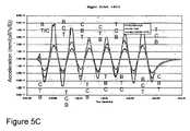
- FIGS. 5A-5Care the outputs of a computer simulation showing trajectories and accelerations of model devices using fields of +/ ⁇ 100V, +/ ⁇ 200V and +/ ⁇ 300V, respectively;
- FIG. 6is a top-view, high-level conceptual representation of a charged particle moving through a series of alternating electric fields according to a first embodiment of the present invention such that photons are emitted in phase with each other;
- FIG. 7is a top-view, high-level conceptual representation of a charged particle moving through a series of alternating electric fields according to a second embodiment of the present invention that includes a focusing element;
- FIG. 8is a top-view, high-level conceptual representation of a charged particle moving through a series of alternating electric fields according to a third embodiment of the present invention that includes a pre-bunching element;
- FIGS. 9A through 9Hare exemplary resonant structures acting as pre-bunching elements.
- FIG. 1is a high-level conceptual representation of a charged particle moving through a series of alternating electric fields according to a first embodiment of the present invention.
- a charged particle beam 100 including charged particles 110e.g., electrons
- the charged particle beam 100can include ions (positive or negative), electrons, protons and the like.
- the beammay be produced by any source, including, e.g., without limitation an ion gun, a thermionic filament, a tungsten filament, a cathode, a planar vacuum triode, an electron-impact ionizer, a laser ionizer, a chemical ionizer, a thermal ionizer, an ion-impact ionizer)
- a sourceincluding, e.g., without limitation an ion gun, a thermionic filament, a tungsten filament, a cathode, a planar vacuum triode, an electron-impact ionizer, a laser ionizer, a chemical ionizer, a thermal ionizer, an ion-impact ionizer
- each positive electric field 130 pis surrounded by a negative electric field 130 n on three sides.
- each negative electric field 130 nis surrounded by a positive field 130 p on three sides.
- the charged particles 110are electrons which are attracted to the positive electric fields 130 p and repelled by the negative electric fields 130 n . The attraction of the charged particles 110 to their oppositely charged fields 130 p or 130 n accelerates the charged particles 110 transversely to their axial velocity.
- the series of alternating fieldscreates an oscillating path in the directions of top to bottom of FIG. 1 and as indicated by the legend “velocity oscillation direction.”
- the velocity oscillation directionis generally perpendicular to the direction of motion of the beam 100 .
- the charged particle source 120may also optionally include one or more electrically biased electrodes 140 (e.g., (a) grounding electrodes or (b) positively biased electrodes) which help to keep the charged particles (e.g., (a) electrons or negatively charged ions or (b) positively charged ions) on the desired path.
- electrically biased electrodes 140e.g., (a) grounding electrodes or (b) positively biased electrodes
- the charged particlese.g., (a) electrons or negatively charged ions or (b) positively charged ions
- FIGS. 2 and 3various elements from FIG. 1 have been repeated, and their reference numerals are repeated in FIGS. 2 and 3 .
- the order of the electric fields 130 p and 130 n below the path of the charged particle beam 100has been changed.
- FIGS. 2 and 3while the electric fields 130 n and 130 p are still alternating on the same side, they are now the same polarity on opposite sides of the beam 100 .
- the electron 100 a in FIG. 2is an accelerating electron that is being accelerated by being repelled from the negative fields 130 n 2 while being attracted to the next positive fields 130 p 3 in the direction of motion of the beam 100 .
- the direction of accelerationis shown below the accelerating electron 100 a.
- the electron 100 d in FIG. 2is a decelerating electron that is being decelerated (i.e., negatively accelerated) as it approaches the negative fields 130 n 4 while still being attracted to the previous positive fields 130 p 3 .
- the direction of accelerationis shown below the decelerating electron 100 d .
- both FIGS. 2 and 3include the legend “velocity oscillation direction” showing the direction of the velocity changes. In such cases, the velocity oscillation direction is generally parallel to the direction of motion of the beam 100 .
- the strengths of adjacent electric fields, fields on the same side of the beam 100 and fields on opposite sides of the beam 100need not be the same strength.
- the strengths of the fields and the polarities of the fieldsneed not be fixed either but may instead vary with time.
- the fields 130 n and 130 pmay even be created by applying a electromagnetic wave to a resonant structure, described in greater detail below.
- the electric fields utilized by the present inventioncan be created by any known method which allows sufficiently fine-grained control over the paths of the charged particles that they stay within intended path boundaries.
- the electric fieldscan be generated using at least one resonant structure where the resonant structure resonates at a frequency above a microwave frequency.
- Resonant structuresinclude resonant structures shown in or constructed by the teachings of the above-identified co-pending applications.
- the structures and methods of U.S. application Ser. No. 11/243,477entitled “Electron Beam Induced Resonance,” filed on Oct. 5, 2005, can be utilized to create electric fields 130 for use in the present invention.
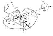
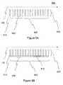
- FIG. 4is a perspective-view, high-level conceptual representation of a charged particle moving through a series of alternating electric fields produced by a resonant structure (RS) 402 (e.g., a microwave resonant structure or an optical resonant structure).
- a resonant structuree.g., a microwave resonant structure or an optical resonant structure.
- An electromagnetic wave 406 (also denoted E) incident to a surface 404 of the RS 402transfers energy to the RS 402 , which generates a varying field 407 .
- a gap 410 formed by ledge portions 412can act as an intensifier.
- the varying field 407is shown across the gap 410 with the electric and magnetic field components (denoted ⁇ right arrow over (E) ⁇ and ⁇ right arrow over (B) ⁇ ) generally along the X and Y axes of the coordinate system, respectively. Since a portion of the varying field can be intensified across the gap 410 , the ledge portions 412 can be sized during fabrication to provide a particular magnitude or wavelength of the varying field 407 .
- a charged particle source 414targets a beam 416 (such as a beam 100 ) of charged particles (e.g., electrons) along a straight path 420 through an opening 422 on a sidewall 424 of the device 400 .
- the charged particlestravel through a space 426 within the gap 410 .
- the charged particlesare shown angularly modulated from the straight path 420 .
- the charged particlestravel on an oscillating path 428 within the gap 410 .
- the charged particlesAfter passing through the gap 410 , the charged particles are angularly modulated on a new path 430 .
- An angle ⁇illustrates the deviation between the new path 430 and the straight path 420 .
- a number of resonant structures 402can be repeated to provide additional electric fields for influencing the charged particles of the beam 416 .
- the direction of the oscillationcan be changed by turning the resonant structure 402 on its side onto surface 404 .
- FIGS. 5A-5Care outputs of computer simulations showing trajectories and accelerations of model devices according to the present invention.
- the outputsillustrate three exemplary paths, labeled “B”, “T” and “C” for bottom, top and center, respectively. As shown on FIG. 1 , these correspond to charged particles passing through the bottom, top and center, respectively, of the opening between the electrodes 140 . Since the curves for B, T and C cross in various locations, the graphs are labeled in various locations.
- the calculationsshow accelerations of about 0.5 ⁇ 10 11 mm/ ⁇ S 2 for electrons with 1 keV of energy passing through a field of +/ ⁇ 100 volts when passing through the center of the electrodes.
- FIG. 5Athe calculations show accelerations of about 0.5 ⁇ 10 11 mm/ ⁇ S 2 for electrons with 1 keV of energy passing through a field of +/ ⁇ 100 volts when passing through the center of the electrodes.
- FIG. 5Bshows accelerations of about 1.0 ⁇ 10 11 mM/ ⁇ S 2 for electrons with 1 keV of energy passing through a field of +/ ⁇ 200 volts when passing through the center of the electrodes.
- FIG. 5Cshows accelerations of about 1.0-3.0 ⁇ 10 11 mm/ ⁇ S 2 for electrons with 1 keV of energy passing through a field of +/ ⁇ 300 volts when passing through the center of the electrodes.
- the electrodeof such a size and spacing that they resonate at or near the frequency that is being generated. This effect can be used to enhance the applied fields in the frequency range that the device emits.
- the oscillating charged particlesemit photons to achieve a radiation emitting device.
- Such photonscan be used to provide radiation to an outside of the device or to produce radiation for use internal to the device as well.
- the amount of radiation producedcan be used as part of measurement devices.
- FIG. 6the structure of FIG. 1 has been supplemented with the addition of photons 600 a - 600 c .
- the electric fields 130 p and 130 nare selected such that the charged particles 110 are moved in an oscillating trajectory at (or nearly at) an integral multiple of the emitted wavelength.
- the electromagnetic radiation emitted at the maxima and minima of the oscillationconstructively interfere with the emission at the next minimum or maximum.
- the photon emissionsare in phase with each other. This produces a coherent radiation source that can be used in laser applications. Exemplary uses of laser include illuminating and cutting.
- a focusing element 700is added in close proximity to the electrodes 140 .
- the focusing element 700while illustrated before the electrodes 140 may instead be placed after. In such a configuration, additional charged particles may traverse a center path between the fields and undergo constructive interference.
- a pre-bunching element 800is added which helps to control the inter-arrival time between charged particles, and therefore aid in the production of coherent Electromagnetic Radiation (EMR).
- EMRElectromagnetic Radiation
- One possible configuration of a pre-bunching element 800is a resonant structure such as is described in U.S. application Ser. No. 11/410,924, entitled “Selectable Frequency EMR Emitter,” filed on even date herewith and incorporated herein by reference.
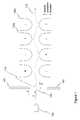
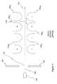
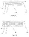
- exemplary resonant structuresare shown in FIGS. 9A-9H . As shown in FIG.
- a resonant structure 910may comprise a series of fingers 915 which are separated by a spacing 920 measured as the beginning of one finger 915 to the beginning of an adjacent finger 915 .
- the finger 915has a thickness that takes up a portion of the spacing between fingers 915 .
- the fingersalso have a length 925 and a height (not shown). As illustrated, the fingers of FIG. 9A are perpendicular to the beam 100 .
- Resonant structures 910are fabricated from resonating material (e.g., from a conductor such as metal (e.g., silver, gold, aluminum and platinum or from an alloy) or from any other material that resonates in the presence of a charged particle beam).
- resonating materiale.g., from a conductor such as metal (e.g., silver, gold, aluminum and platinum or from an alloy) or from any other material that resonates in the presence of a charged particle beam.
- Other exemplary resonating materialsinclude carbon nanotubes and high temperature superconductors.
- any of the various resonant structurescan be constructed in multiple layers of resonating materials but are preferably constructed in a single layer of resonating material (as described above).
- all of the parts of a resonant structure 910are etched or otherwise shaped in the same processing step.
- resonant structures 910 of the same resonant frequencyare etched or otherwise shaped in the same processing step.
- all resonant structures having segments of the same heightare etched or otherwise shaped in the same processing step.
- all of the resonant structures on a single substrateare etched or otherwise shaped in the same processing step.
- the materialneed not even be a contiguous layer, but can be a series of resonant elements individually present on a substrate.
- the materials making up the resonant elementscan be produced by a variety of methods, such as by pulsed-plating, depositing, sputtering or etching. Preferred methods for doing so are described in co-pending U.S. application Ser. No. 10/917,571, filed on Aug. 13, 2004, entitled “Patterning Thin Metal Film by Dry Reactive Ion Etching,” and in U.S. application Ser. No. 11/203,407, filed on Aug. 15, 2005, entitled “Method Of Patterning Ultra-Small Structures,” both of which are commonly owned at the time of filing, and the entire contents of each of which are incorporated herein by reference.
- etchingdoes not need to remove the material between segments or posts all the way down to the substrate level, nor does the plating have to place the posts directly on the substrate.
- Silver postscan be on a silver layer on top of the substrate. In fact, we discovered that, due to various coupling effects, better results are obtained when the silver posts are set on a silver layer, which itself is on the substrate.
- the fingers of the resonant structure 910can be supplemented with a backbone.
- the backbone 912connects the various fingers 915 of the resonant structure 910 forming a comb-like shape on its side.
- the backbone 912would be made of the same material as the rest of the resonant structure 910 , but alternate materials may be used.
- the backbone 912may be formed in the same layer or a different layer than the fingers 910 .
- the backbone 912may also be formed in the same processing step or in a different processing step than the fingers 915 . While the remaining figures do not show the use of a backbone 912 , it should be appreciated that all other resonant structures described herein can be fabricated with a backbone also.
- the shape of the fingers 915may also be shapes other than rectangles, such as simple shapes (e.g., circles, ovals, arcs and squares), complex shapes (e.g., such as semi-circles, angled fingers, serpentine structures and embedded structures (i.e., structures with a smaller geometry within a larger geometry, thereby creating more complex resonances)) and those including waveguides or complex cavities.
- the finger structures of all the various shapeswill be collectively referred to herein as “segments.”
- Other exemplary shapesare shown in FIGS. 9C-9H , again with respect to a path of a beam 100 . As can be seen at least from FIG. 9C , the axis of symmetry of the segments need not be perpendicular to the path of the beam 100 .
- Exemplary dimensions for resonant structuresinclude, but are not limited to:
- Such a methodincludes: generating a beam of charged particles; providing a series of alternating electric fields along an intended path; and transmitting the beam of charged particles along the intended path through the alternating electric fields.
- the resonant structures producing coherent light described abovecan be laid out in rows, columns, arrays or other configurations such that the intensity of the resulting EMR is increased.
- the coherent EMR producedmay additionally be used as an input to additional devices.
- the coherent EMRmay be used as an input to a light amplifier or may be used as part of transmission system.
Landscapes
- Physics & Mathematics (AREA)
- Engineering & Computer Science (AREA)
- Plasma & Fusion (AREA)
- Optics & Photonics (AREA)
- Spectroscopy & Molecular Physics (AREA)
- Electromagnetism (AREA)
- Particle Accelerators (AREA)
Abstract
Description
- (a) period (920) of segments: 150-220 nm;
- (b) segment thickness: 75-110 nm;
- (c) height of segments: 250-400 nm;
- (d) length (925) of segments: 60-180 nm; and
- (e) number of segments in a row: 200-300.
Claims (21)
Priority Applications (1)
| Application Number | Priority Date | Filing Date | Title |
|---|---|---|---|
| US11/411,129US7876793B2 (en) | 2006-04-26 | 2006-04-26 | Micro free electron laser (FEL) |
Applications Claiming Priority (1)
| Application Number | Priority Date | Filing Date | Title |
|---|---|---|---|
| US11/411,129US7876793B2 (en) | 2006-04-26 | 2006-04-26 | Micro free electron laser (FEL) |
Publications (2)
| Publication Number | Publication Date |
|---|---|
| US20090290604A1 US20090290604A1 (en) | 2009-11-26 |
| US7876793B2true US7876793B2 (en) | 2011-01-25 |
Family
ID=41342082
Family Applications (1)
| Application Number | Title | Priority Date | Filing Date |
|---|---|---|---|
| US11/411,129Expired - Fee RelatedUS7876793B2 (en) | 2006-04-26 | 2006-04-26 | Micro free electron laser (FEL) |
Country Status (1)
| Country | Link |
|---|---|
| US (1) | US7876793B2 (en) |
Cited By (7)
| Publication number | Priority date | Publication date | Assignee | Title |
|---|---|---|---|---|
| US20070272931A1 (en)* | 2006-05-05 | 2007-11-29 | Virgin Islands Microsystems, Inc. | Methods, devices and systems producing illumination and effects |
| US20090072698A1 (en)* | 2007-06-19 | 2009-03-19 | Virgin Islands Microsystems, Inc. | Microwave coupled excitation of solid state resonant arrays |
| US20090140178A1 (en)* | 2006-01-05 | 2009-06-04 | Virgin Islands Microsystems, Inc. | Switching micro-resonant structures by modulating a beam of charged particles |
| US9054491B1 (en) | 2012-02-10 | 2015-06-09 | Walter C. Hurlbut | Solid-state coherent electromagnetic radiation source |
| US9466940B2 (en) | 2012-07-26 | 2016-10-11 | Huawei Technologies Co., Ltd | Graphene illuminator, and heat dissipating apparatus and optical transmission network node using the graphene illuminator |
| US20180287329A1 (en)* | 2017-04-03 | 2018-10-04 | Massachusetts Institute Of Technology | Apparatus and methods for generating and enhancing smith-purcell radiation |
| US20230191916A1 (en)* | 2021-12-20 | 2023-06-22 | Micah Skidmore | Novel electromagnetic propulsion and levitation technology |
Families Citing this family (1)
| Publication number | Priority date | Publication date | Assignee | Title |
|---|---|---|---|---|
| WO2013126896A1 (en)* | 2012-02-24 | 2013-08-29 | The Regents Of The University Of California | Charged particle acceleration device |
Citations (318)
| Publication number | Priority date | Publication date | Assignee | Title |
|---|---|---|---|---|
| US1948384A (en) | 1932-01-26 | 1934-02-20 | Research Corp | Method and apparatus for the acceleration of ions |
| US2307086A (en) | 1941-05-07 | 1943-01-05 | Univ Leland Stanford Junior | High frequency electrical apparatus |
| US2431396A (en) | 1942-12-21 | 1947-11-25 | Rca Corp | Current magnitude-ratio responsive amplifier |
| US2473477A (en) | 1946-07-24 | 1949-06-14 | Raythcon Mfg Company | Magnetic induction device |
| US2634372A (en) | 1953-04-07 | Super high-frequency electromag | ||
| US2932798A (en) | 1956-01-05 | 1960-04-12 | Research Corp | Imparting energy to charged particles |
| US2944183A (en) | 1957-01-25 | 1960-07-05 | Bell Telephone Labor Inc | Internal cavity reflex klystron tuned by a tightly coupled external cavity |
| US2966611A (en) | 1959-07-21 | 1960-12-27 | Sperry Rand Corp | Ruggedized klystron tuner |
| US3231779A (en) | 1962-06-25 | 1966-01-25 | Gen Electric | Elastic wave responsive apparatus |
| US3274428A (en) | 1962-06-29 | 1966-09-20 | English Electric Valve Co Ltd | Travelling wave tube with band pass slow wave structure whose frequency characteristic changes along its length |
| US3297905A (en) | 1963-02-06 | 1967-01-10 | Varian Associates | Electron discharge device of particular materials for stabilizing frequency and reducing magnetic field problems |
| US3315117A (en)* | 1963-07-15 | 1967-04-18 | Burton J Udelson | Electrostatically focused electron beam phase shifter |
| US3387169A (en) | 1965-05-07 | 1968-06-04 | Sfd Lab Inc | Slow wave structure of the comb type having strap means connecting the teeth to form iterative inductive shunt loadings |
| US3543147A (en) | 1968-03-29 | 1970-11-24 | Atomic Energy Commission | Phase angle measurement system for determining and controlling the resonance of the radio frequency accelerating cavities for high energy charged particle accelerators |
| US3546524A (en) | 1967-11-24 | 1970-12-08 | Varian Associates | Linear accelerator having the beam injected at a position of maximum r.f. accelerating field |
| US3560694A (en) | 1969-01-21 | 1971-02-02 | Varian Associates | Microwave applicator employing flat multimode cavity for treating webs |
| US3571642A (en) | 1968-01-17 | 1971-03-23 | Ca Atomic Energy Ltd | Method and apparatus for interleaved charged particle acceleration |
| US3586899A (en) | 1968-06-12 | 1971-06-22 | Ibm | Apparatus using smith-purcell effect for frequency modulation and beam deflection |
| US3761828A (en) | 1970-12-10 | 1973-09-25 | J Pollard | Linear particle accelerator with coast through shield |
| US3886399A (en) | 1973-08-20 | 1975-05-27 | Varian Associates | Electron beam electrical power transmission system |
| US3923568A (en) | 1974-01-14 | 1975-12-02 | Int Plasma Corp | Dry plasma process for etching noble metal |
| US3989347A (en) | 1974-06-20 | 1976-11-02 | Siemens Aktiengesellschaft | Acousto-optical data input transducer with optical data storage and process for operation thereof |
| US4053845A (en) | 1967-03-06 | 1977-10-11 | Gordon Gould | Optically pumped laser amplifiers |
| US4269672A (en) | 1979-06-01 | 1981-05-26 | Inoue-Japax Research Incorporated | Gap distance control electroplating |
| US4282436A (en) | 1980-06-04 | 1981-08-04 | The United States Of America As Represented By The Secretary Of The Navy | Intense ion beam generation with an inverse reflex tetrode (IRT) |
| US4296354A (en) | 1979-11-28 | 1981-10-20 | Varian Associates, Inc. | Traveling wave tube with frequency variable sever length |
| US4450554A (en) | 1981-08-10 | 1984-05-22 | International Telephone And Telegraph Corporation | Asynchronous integrated voice and data communication system |
| US4453108A (en) | 1980-11-21 | 1984-06-05 | William Marsh Rice University | Device for generating RF energy from electromagnetic radiation of another form such as light |
| US4482779A (en) | 1983-04-19 | 1984-11-13 | The United States Of America As Represented By The Administrator Of National Aeronautics And Space Administration | Inelastic tunnel diodes |
| US4528659A (en) | 1981-12-17 | 1985-07-09 | International Business Machines Corporation | Interleaved digital data and voice communications system apparatus and method |
| US4589107A (en) | 1982-11-30 | 1986-05-13 | Itt Corporation | Simultaneous voice and data communication and data base access in a switching system using a combined voice conference and data base processing module |
| US4598397A (en) | 1984-02-21 | 1986-07-01 | Cxc Corporation | Microtelephone controller |
| US4630262A (en) | 1984-05-23 | 1986-12-16 | International Business Machines Corp. | Method and system for transmitting digitized voice signals as packets of bits |
| US4652703A (en) | 1983-03-01 | 1987-03-24 | Racal Data Communications Inc. | Digital voice transmission having improved echo suppression |
| US4661783A (en) | 1981-03-18 | 1987-04-28 | The United States Of America As Represented By The Secretary Of The Navy | Free electron and cyclotron resonance distributed feedback lasers and masers |
| US4704583A (en) | 1974-08-16 | 1987-11-03 | Gordon Gould | Light amplifiers employing collisions to produce a population inversion |
| US4712042A (en) | 1986-02-03 | 1987-12-08 | Accsys Technology, Inc. | Variable frequency RFQ linear accelerator |
| US4713581A (en) | 1983-08-09 | 1987-12-15 | Haimson Research Corporation | Method and apparatus for accelerating a particle beam |
| US4727550A (en)* | 1985-09-19 | 1988-02-23 | Chang David B | Radiation source |
| US4740963A (en) | 1986-01-30 | 1988-04-26 | Lear Siegler, Inc. | Voice and data communication system |
| US4740973A (en) | 1984-05-21 | 1988-04-26 | Madey John M J | Free electron laser |
| US4746201A (en) | 1967-03-06 | 1988-05-24 | Gordon Gould | Polarizing apparatus employing an optical element inclined at brewster's angle |
| US4761059A (en) | 1986-07-28 | 1988-08-02 | Rockwell International Corporation | External beam combining of multiple lasers |
| US4782485A (en) | 1985-08-23 | 1988-11-01 | Republic Telcom Systems Corporation | Multiplexed digital packet telephone system |
| US4789945A (en) | 1985-07-29 | 1988-12-06 | Advantest Corporation | Method and apparatus for charged particle beam exposure |
| US4806859A (en) | 1987-01-27 | 1989-02-21 | Ford Motor Company | Resonant vibrating structures with driving sensing means for noncontacting position and pick up sensing |
| US4809271A (en) | 1986-11-14 | 1989-02-28 | Hitachi, Ltd. | Voice and data multiplexer system |
| US4813040A (en) | 1986-10-31 | 1989-03-14 | Futato Steven P | Method and apparatus for transmitting digital data and real-time digitalized voice information over a communications channel |
| US4819228A (en) | 1984-10-29 | 1989-04-04 | Stratacom Inc. | Synchronous packet voice/data communication system |
| US4829527A (en) | 1984-04-23 | 1989-05-09 | The United States Of America As Represented By The Secretary Of The Army | Wideband electronic frequency tuning for orotrons |
| US4838021A (en) | 1987-12-11 | 1989-06-13 | Hughes Aircraft Company | Electrostatic ion thruster with improved thrust modulation |
| US4841538A (en) | 1986-03-05 | 1989-06-20 | Kabushiki Kaisha Toshiba | CO2 gas laser device |
| US4864575A (en)* | 1988-12-06 | 1989-09-05 | The United States Of America As Represented By The Secretary Of The Air Force | Static periodic field device for free electron laser |
| US4864131A (en) | 1987-11-09 | 1989-09-05 | The University Of Michigan | Positron microscopy |
| US4866732A (en) | 1985-02-04 | 1989-09-12 | Mitel Telecom Limited | Wireless telephone system |
| US4866704A (en) | 1988-03-16 | 1989-09-12 | California Institute Of Technology | Fiber optic voice/data network |
| US4873715A (en) | 1986-06-10 | 1989-10-10 | Hitachi, Ltd. | Automatic data/voice sending/receiving mode switching device |
| US4887265A (en) | 1988-03-18 | 1989-12-12 | Motorola, Inc. | Packet-switched cellular telephone system |
| US4890282A (en) | 1988-03-08 | 1989-12-26 | Network Equipment Technologies, Inc. | Mixed mode compression for data transmission |
| US4898022A (en) | 1987-02-09 | 1990-02-06 | Tlv Co., Ltd. | Steam trap operation detector |
| US4912705A (en) | 1985-03-20 | 1990-03-27 | International Mobile Machines Corporation | Subscriber RF telephone system for providing multiple speech and/or data signals simultaneously over either a single or a plurality of RF channels |
| US4932022A (en) | 1987-10-07 | 1990-06-05 | Telenova, Inc. | Integrated voice and data telephone system |
| US4981371A (en) | 1989-02-17 | 1991-01-01 | Itt Corporation | Integrated I/O interface for communication terminal |
| US5023563A (en)* | 1989-06-08 | 1991-06-11 | Hughes Aircraft Company | Upshifted free electron laser amplifier |
| US5036513A (en) | 1989-06-21 | 1991-07-30 | Academy Of Applied Science | Method of and apparatus for integrated voice (audio) communication simultaneously with "under voice" user-transparent digital data between telephone instruments |
| US5065425A (en) | 1988-12-23 | 1991-11-12 | Telic Alcatel | Telephone connection arrangement for a personal computer and a device for such an arrangement |
| US5113141A (en) | 1990-07-18 | 1992-05-12 | Science Applications International Corporation | Four-fingers RFQ linac structure |
| US5121385A (en) | 1988-09-14 | 1992-06-09 | Fujitsu Limited | Highly efficient multiplexing system |
| US5127001A (en) | 1990-06-22 | 1992-06-30 | Unisys Corporation | Conference call arrangement for distributed network |
| US5128729A (en) | 1990-11-13 | 1992-07-07 | Motorola, Inc. | Complex opto-isolator with improved stand-off voltage stability |
| US5130985A (en) | 1988-11-25 | 1992-07-14 | Hitachi, Ltd. | Speech packet communication system and method |
| US5150410A (en) | 1991-04-11 | 1992-09-22 | Itt Corporation | Secure digital conferencing system |
| US5155726A (en) | 1990-01-22 | 1992-10-13 | Digital Equipment Corporation | Station-to-station full duplex communication in a token ring local area network |
| US5157000A (en) | 1989-07-10 | 1992-10-20 | Texas Instruments Incorporated | Method for dry etching openings in integrated circuit layers |
| US5163118A (en) | 1986-11-10 | 1992-11-10 | The United States Of America As Represented By The Secretary Of The Air Force | Lattice mismatched hetrostructure optical waveguide |
| US5185073A (en) | 1988-06-21 | 1993-02-09 | International Business Machines Corporation | Method of fabricating nendritic materials |
| US5187591A (en) | 1991-01-24 | 1993-02-16 | Micom Communications Corp. | System for transmitting and receiving aural information and modulated data |
| US5199918A (en) | 1991-11-07 | 1993-04-06 | Microelectronics And Computer Technology Corporation | Method of forming field emitter device with diamond emission tips |
| US5214650A (en) | 1990-11-19 | 1993-05-25 | Ag Communication Systems Corporation | Simultaneous voice and data system using the existing two-wire inter-face |
| US5233623A (en) | 1992-04-29 | 1993-08-03 | Research Foundation Of State University Of New York | Integrated semiconductor laser with electronic directivity and focusing control |
| US5235248A (en) | 1990-06-08 | 1993-08-10 | The United States Of America As Represented By The United States Department Of Energy | Method and split cavity oscillator/modulator to generate pulsed particle beams and electromagnetic fields |
| WO1993021663A1 (en) | 1992-04-08 | 1993-10-28 | Georgia Tech Research Corporation | Process for lift-off of thin film materials from a growth substrate |
| US5263043A (en) | 1990-08-31 | 1993-11-16 | Trustees Of Dartmouth College | Free electron laser utilizing grating coupling |
| US5262656A (en) | 1991-06-07 | 1993-11-16 | Thomson-Csf | Optical semiconductor transceiver with chemically resistant layers |
| US5268693A (en) | 1990-08-31 | 1993-12-07 | Trustees Of Dartmouth College | Semiconductor film free electron laser |
| US5268788A (en) | 1991-06-25 | 1993-12-07 | Smiths Industries Public Limited Company | Display filter arrangements |
| US5282197A (en) | 1992-05-15 | 1994-01-25 | International Business Machines | Low frequency audio sub-channel embedded signalling |
| US5283819A (en) | 1991-04-25 | 1994-02-01 | Compuadd Corporation | Computing and multimedia entertainment system |
| US5293175A (en) | 1991-07-19 | 1994-03-08 | Conifer Corporation | Stacked dual dipole MMDS feed |
| US5302240A (en) | 1991-01-22 | 1994-04-12 | Kabushiki Kaisha Toshiba | Method of manufacturing semiconductor device |
| US5305312A (en) | 1992-02-07 | 1994-04-19 | At&T Bell Laboratories | Apparatus for interfacing analog telephones and digital data terminals to an ISDN line |
| US5341374A (en) | 1991-03-01 | 1994-08-23 | Trilan Systems Corporation | Communication network integrating voice data and video with distributed call processing |
| US5446814A (en) | 1993-11-05 | 1995-08-29 | Motorola | Molded reflective optical waveguide |
| US5485277A (en) | 1994-07-26 | 1996-01-16 | Physical Optics Corporation | Surface plasmon resonance sensor and methods for the utilization thereof |
| US5504341A (en) | 1995-02-17 | 1996-04-02 | Zimec Consulting, Inc. | Producing RF electric fields suitable for accelerating atomic and molecular ions in an ion implantation system |
| US5578909A (en) | 1994-07-15 | 1996-11-26 | The Regents Of The Univ. Of California | Coupled-cavity drift-tube linac |
| US5604352A (en) | 1995-04-25 | 1997-02-18 | Raychem Corporation | Apparatus comprising voltage multiplication components |
| US5608263A (en) | 1994-09-06 | 1997-03-04 | The Regents Of The University Of Michigan | Micromachined self packaged circuits for high-frequency applications |
| US5637966A (en) | 1995-02-06 | 1997-06-10 | The Regents Of The University Of Michigan | Method for generating a plasma wave to accelerate electrons |
| US5663971A (en) | 1996-04-02 | 1997-09-02 | The Regents Of The University Of California, Office Of Technology Transfer | Axial interaction free-electron laser |
| US5666020A (en) | 1994-11-16 | 1997-09-09 | Nec Corporation | Field emission electron gun and method for fabricating the same |
| US5668368A (en) | 1992-02-21 | 1997-09-16 | Hitachi, Ltd. | Apparatus for suppressing electrification of sample in charged beam irradiation apparatus |
| US5705443A (en) | 1995-05-30 | 1998-01-06 | Advanced Technology Materials, Inc. | Etching method for refractory materials |
| US5737458A (en) | 1993-03-29 | 1998-04-07 | Martin Marietta Corporation | Optical light pipe and microwave waveguide interconnects in multichip modules formed using adaptive lithography |
| US5744919A (en) | 1996-12-12 | 1998-04-28 | Mishin; Andrey V. | CW particle accelerator with low particle injection velocity |
| US5757009A (en) | 1996-12-27 | 1998-05-26 | Northrop Grumman Corporation | Charged particle beam expander |
| US5767013A (en) | 1996-08-26 | 1998-06-16 | Lg Semicon Co., Ltd. | Method for forming interconnection in semiconductor pattern device |
| US5780970A (en) | 1996-10-28 | 1998-07-14 | University Of Maryland | Multi-stage depressed collector for small orbit gyrotrons |
| US5790585A (en) | 1996-11-12 | 1998-08-04 | The Trustees Of Dartmouth College | Grating coupling free electron laser apparatus and method |
| US5811943A (en) | 1996-09-23 | 1998-09-22 | Schonberg Research Corporation | Hollow-beam microwave linear accelerator |
| US5821902A (en) | 1993-09-02 | 1998-10-13 | Inmarsat | Folded dipole microstrip antenna |
| US5821836A (en) | 1997-05-23 | 1998-10-13 | The Regents Of The University Of Michigan | Miniaturized filter assembly |
| US5825140A (en) | 1996-02-29 | 1998-10-20 | Nissin Electric Co., Ltd. | Radio-frequency type charged particle accelerator |
| US5831270A (en) | 1996-02-19 | 1998-11-03 | Nikon Corporation | Magnetic deflectors and charged-particle-beam lithography systems incorporating same |
| US5847745A (en) | 1995-03-03 | 1998-12-08 | Futaba Denshi Kogyo K.K. | Optical write element |
| US5858799A (en) | 1995-10-25 | 1999-01-12 | University Of Washington | Surface plasmon resonance chemical electrode |
| US5889797A (en) | 1996-08-26 | 1999-03-30 | The Regents Of The University Of California | Measuring short electron bunch lengths using coherent smith-purcell radiation |
| US5889449A (en) | 1995-12-07 | 1999-03-30 | Space Systems/Loral, Inc. | Electromagnetic transmission line elements having a boundary between materials of high and low dielectric constants |
| US5902489A (en) | 1995-11-08 | 1999-05-11 | Hitachi, Ltd. | Particle handling method by acoustic radiation force and apparatus therefore |
| US5963857A (en) | 1998-01-20 | 1999-10-05 | Lucent Technologies, Inc. | Article comprising a micro-machined filter |
| US5972193A (en) | 1997-10-10 | 1999-10-26 | Industrial Technology Research Institute | Method of manufacturing a planar coil using a transparency substrate |
| US6005347A (en) | 1995-12-12 | 1999-12-21 | Lg Electronics Inc. | Cathode for a magnetron having primary and secondary electron emitters |
| US6008496A (en) | 1997-05-05 | 1999-12-28 | University Of Florida | High resolution resonance ionization imaging detector and method |
| US6040625A (en) | 1997-09-25 | 2000-03-21 | I/O Sensors, Inc. | Sensor package arrangement |
| US6060833A (en) | 1996-10-18 | 2000-05-09 | Velazco; Jose E. | Continuous rotating-wave electron beam accelerator |
| US6080529A (en) | 1997-12-12 | 2000-06-27 | Applied Materials, Inc. | Method of etching patterned layers useful as masking during subsequent etching or for damascene structures |
| US6117784A (en) | 1997-11-12 | 2000-09-12 | International Business Machines Corporation | Process for integrated circuit wiring |
| US6139760A (en) | 1997-12-19 | 2000-10-31 | Electronics And Telecommunications Research Institute | Short-wavelength optoelectronic device including field emission device and its fabricating method |
| US6180415B1 (en) | 1997-02-20 | 2001-01-30 | The Regents Of The University Of California | Plasmon resonant particles, methods and apparatus |
| US6195199B1 (en) | 1997-10-27 | 2001-02-27 | Kanazawa University | Electron tube type unidirectional optical amplifier |
| US6210555B1 (en) | 1999-01-29 | 2001-04-03 | Faraday Technology Marketing Group, Llc | Electrodeposition of metals in small recesses for manufacture of high density interconnects using reverse pulse plating |
| US6222866B1 (en) | 1997-01-06 | 2001-04-24 | Fuji Xerox Co., Ltd. | Surface emitting semiconductor laser, its producing method and surface emitting semiconductor laser array |
| US6278239B1 (en) | 1996-06-25 | 2001-08-21 | The United States Of America As Represented By The United States Department Of Energy | Vacuum-surface flashover switch with cantilever conductors |
| US6297511B1 (en) | 1999-04-01 | 2001-10-02 | Raytheon Company | High frequency infrared emitter |
| US20010025925A1 (en) | 2000-03-28 | 2001-10-04 | Kabushiki Kaisha Toshiba | Charged particle beam system and pattern slant observing method |
| US6301041B1 (en) | 1998-08-18 | 2001-10-09 | Kanazawa University | Unidirectional optical amplifier |
| US6303014B1 (en) | 1998-10-14 | 2001-10-16 | Faraday Technology Marketing Group, Llc | Electrodeposition of metals in small recesses using modulated electric fields |
| US6309528B1 (en) | 1999-10-15 | 2001-10-30 | Faraday Technology Marketing Group, Llc | Sequential electrodeposition of metals using modulated electric fields for manufacture of circuit boards having features of different sizes |
| US6316876B1 (en) | 1998-08-19 | 2001-11-13 | Eiji Tanabe | High gradient, compact, standing wave linear accelerator structure |
| US20010045360A1 (en) | 2000-05-25 | 2001-11-29 | Ryushin Omasa | Electroplating method using combination of vibrational flow in plating bath and plating current of pulse |
| US6338968B1 (en) | 1998-02-02 | 2002-01-15 | Signature Bioscience, Inc. | Method and apparatus for detecting molecular binding events |
| US20020036121A1 (en) | 2000-09-08 | 2002-03-28 | Ronald Ball | Illumination system for escalator handrails |
| US20020036264A1 (en) | 2000-07-27 | 2002-03-28 | Mamoru Nakasuji | Sheet beam-type inspection apparatus |
| US6370306B1 (en) | 1997-12-15 | 2002-04-09 | Seiko Instruments Inc. | Optical waveguide probe and its manufacturing method |
| US6373194B1 (en) | 2000-06-01 | 2002-04-16 | Raytheon Company | Optical magnetron for high efficiency production of optical radiation |
| US20020053638A1 (en) | 1998-07-03 | 2002-05-09 | Dieter Winkler | Apparatus and method for examing specimen with a charged particle beam |
| US20020056645A1 (en) | 1998-10-14 | 2002-05-16 | Taylor E. Jennings | Electrodeposition of metals in small recesses using modulated electric fields |
| US20020068018A1 (en) | 2000-12-06 | 2002-06-06 | Hrl Laboratories, Llc | Compact sensor using microcavity structures |
| US20020071457A1 (en) | 2000-12-08 | 2002-06-13 | Hogan Josh N. | Pulsed non-linear resonant cavity |
| US6407516B1 (en) | 2000-05-26 | 2002-06-18 | Exaconnect Inc. | Free space electron switch |
| US6441298B1 (en) | 2000-08-15 | 2002-08-27 | Nec Research Institute, Inc | Surface-plasmon enhanced photovoltaic device |
| US20020122531A1 (en) | 2001-03-05 | 2002-09-05 | Siemens Medical Systems, Inc. | Multi-mode operation of a standing wave linear accelerator |
| US6448850B1 (en) | 1999-05-20 | 2002-09-10 | Kanazawa University | Electromagnetic wave amplifier and electromagnetic wave generator |
| US6453087B2 (en) | 2000-04-28 | 2002-09-17 | Confluent Photonics Co. | Miniature monolithic optical add-drop multiplexer |
| US20020135665A1 (en) | 2001-03-20 | 2002-09-26 | Keith Gardner | Led print head for electrophotographic printer |
| US20020139961A1 (en) | 2001-03-23 | 2002-10-03 | Fuji Photo Film Co., Ltd. | Molecular electric wire, molecular electric wire circuit using the same and process for producing the molecular electric wire circuit |
| US6470198B1 (en) | 1999-04-28 | 2002-10-22 | Murata Manufacturing Co., Ltd. | Electronic part, dielectric resonator, dielectric filter, duplexer, and communication device comprised of high TC superconductor |
| US20020158295A1 (en) | 2001-03-07 | 2002-10-31 | Marten Armgarth | Electrochemical device |
| US20020191650A1 (en)* | 2001-02-26 | 2002-12-19 | Madey John M. J. | Phase displacement free-electron laser |
| US20030010979A1 (en) | 2000-01-14 | 2003-01-16 | Fabrice Pardo | Vertical metal-semiconductor microresonator photodetecting device and production method thereof |
| US20030012925A1 (en) | 2001-07-16 | 2003-01-16 | Motorola, Inc. | Process for fabricating semiconductor structures and devices utilizing the formation of a compliant substrate for materials used to form the same and including an etch stop layer used for back side processing |
| US20030016421A1 (en) | 2000-06-01 | 2003-01-23 | Small James G. | Wireless communication system with high efficiency/high power optical source |
| US20030034535A1 (en) | 2001-08-15 | 2003-02-20 | Motorola, Inc. | Mems devices suitable for integration with chip having integrated silicon and compound semiconductor devices, and methods for fabricating such devices |
| US6525477B2 (en) | 2001-05-29 | 2003-02-25 | Raytheon Company | Optical magnetron generator |
| US6545425B2 (en) | 2000-05-26 | 2003-04-08 | Exaconnect Corp. | Use of a free space electron switch in a telecommunications network |
| US6552320B1 (en) | 1999-06-21 | 2003-04-22 | United Microelectronics Corp. | Image sensor structure |
| US20030103150A1 (en) | 2001-11-30 | 2003-06-05 | Catrysse Peter B. | Integrated color pixel ( ICP ) |
| US6577040B2 (en) | 1999-01-14 | 2003-06-10 | The Regents Of The University Of Michigan | Method and apparatus for generating a signal having at least one desired output frequency utilizing a bank of vibrating micromechanical devices |
| US20030106998A1 (en) | 1996-08-08 | 2003-06-12 | William Marsh Rice University | Method for producing boron nitride coatings and fibers and compositions thereof |
| US6580075B2 (en) | 1998-09-18 | 2003-06-17 | Hitachi, Ltd. | Charged particle beam scanning type automatic inspecting apparatus |
| US6603915B2 (en) | 2001-02-05 | 2003-08-05 | Fujitsu Limited | Interposer and method for producing a light-guiding structure |
| US6603781B1 (en) | 2001-01-19 | 2003-08-05 | Siros Technologies, Inc. | Multi-wavelength transmitter |
| US20030158474A1 (en) | 2002-01-18 | 2003-08-21 | Axel Scherer | Method and apparatus for nanomagnetic manipulation and sensing |
| US20030155521A1 (en) | 2000-02-01 | 2003-08-21 | Hans-Peter Feuerbaum | Optical column for charged particle beam device |
| US20030164947A1 (en) | 2000-04-18 | 2003-09-04 | Matthias Vaupel | Spr sensor |
| US6624916B1 (en) | 1997-02-11 | 2003-09-23 | Quantumbeam Limited | Signalling system |
| US20030179974A1 (en) | 2002-03-20 | 2003-09-25 | Estes Michael J. | Surface plasmon devices |
| US6636185B1 (en) | 1992-03-13 | 2003-10-21 | Kopin Corporation | Head-mounted display system |
| US6636653B2 (en) | 2001-02-02 | 2003-10-21 | Teravicta Technologies, Inc. | Integrated optical micro-electromechanical systems and methods of fabricating and operating the same |
| US6640023B2 (en) | 2001-09-27 | 2003-10-28 | Memx, Inc. | Single chip optical cross connect |
| US6642907B2 (en) | 2001-01-12 | 2003-11-04 | The Furukawa Electric Co., Ltd. | Antenna device |
| US20030206708A1 (en) | 2002-03-20 | 2003-11-06 | Estes Michael J. | Surface plasmon devices |
| US20030214695A1 (en) | 2002-03-18 | 2003-11-20 | E Ink Corporation | Electro-optic displays, and methods for driving same |
| US20030222579A1 (en) | 2001-11-13 | 2003-12-04 | Burle Technologies, Inc. | Photocathode |
| US20040011432A1 (en) | 2002-07-17 | 2004-01-22 | Podlaha Elizabeth J. | Metal alloy electrodeposited microstructures |
| US6687034B2 (en) | 2001-03-23 | 2004-02-03 | Microvision, Inc. | Active tuning of a torsional resonant structure |
| US6700748B1 (en) | 2000-04-28 | 2004-03-02 | International Business Machines Corporation | Methods for creating ground paths for ILS |
| US20040061053A1 (en) | 2001-02-28 | 2004-04-01 | Yoshifumi Taniguchi | Method and apparatus for measuring physical properties of micro region |
| US6724486B1 (en) | 1999-04-28 | 2004-04-20 | Zygo Corporation | Helium- Neon laser light source generating two harmonically related, single- frequency wavelengths for use in displacement and dispersion measuring interferometry |
| US20040080285A1 (en) | 2000-05-26 | 2004-04-29 | Victor Michel N. | Use of a free space electron switch in a telecommunications network |
| US20040085159A1 (en) | 2002-11-01 | 2004-05-06 | Kubena Randall L. | Micro electrical mechanical system (MEMS) tuning using focused ion beams |
| US20040092104A1 (en) | 2002-06-19 | 2004-05-13 | Luxtera, Inc. | Methods of incorporating germanium within CMOS process |
| US6738176B2 (en) | 2002-04-30 | 2004-05-18 | Mario Rabinowitz | Dynamic multi-wavelength switching ensemble |
| US6741781B2 (en) | 2000-09-29 | 2004-05-25 | Kabushiki Kaisha Toshiba | Optical interconnection circuit board and manufacturing method thereof |
| US20040108473A1 (en) | 2000-06-09 | 2004-06-10 | Melnychuk Stephan T. | Extreme ultraviolet light source |
| US20040108471A1 (en) | 2002-09-26 | 2004-06-10 | Chiyan Luo | Photonic crystals: a medium exhibiting anomalous cherenkov radiation |
| US20040108823A1 (en) | 2002-12-09 | 2004-06-10 | Fondazione Per Adroterapia Oncologica - Tera | Linac for ion beam acceleration |
| US20040136715A1 (en) | 2002-12-06 | 2004-07-15 | Seiko Epson Corporation | Wavelength multiplexing on-chip optical interconnection circuit, electro-optical device, and electronic apparatus |
| US20040150991A1 (en) | 2003-01-27 | 2004-08-05 | 3M Innovative Properties Company | Phosphor based light sources utilizing total internal reflection |
| US20040154925A1 (en) | 2003-02-11 | 2004-08-12 | Podlaha Elizabeth J. | Composite metal and composite metal alloy microstructures |
| US6782205B2 (en) | 2001-06-25 | 2004-08-24 | Silicon Light Machines | Method and apparatus for dynamic equalization in wavelength division multiplexing |
| US20040171272A1 (en) | 2003-02-28 | 2004-09-02 | Applied Materials, Inc. | Method of etching metallic materials to form a tapered profile |
| US6791438B2 (en) | 2001-10-30 | 2004-09-14 | Matsushita Electric Industrial Co., Ltd. | Radio frequency module and method for manufacturing the same |
| US20040180244A1 (en) | 2003-01-24 | 2004-09-16 | Tour James Mitchell | Process and apparatus for microwave desorption of elements or species from carbon nanotubes |
| US20040184270A1 (en) | 2003-03-17 | 2004-09-23 | Halter Michael A. | LED light module with micro-reflector cavities |
| US6800877B2 (en) | 2000-05-26 | 2004-10-05 | Exaconnect Corp. | Semi-conductor interconnect using free space electron switch |
| US20040213375A1 (en) | 2003-04-25 | 2004-10-28 | Paul Bjorkholm | Radiation sources and radiation scanning systems with improved uniformity of radiation intensity |
| US20040218651A1 (en) | 2000-03-03 | 2004-11-04 | Canon Kabushiki Kaisha | Electron-beam excitation laser |
| US20040217297A1 (en) | 2000-12-01 | 2004-11-04 | Yeda Research And Development Co. Ltd. | Device and method for the examination of samples in a non vacuum environment using a scanning electron microscope |
| US6819432B2 (en) | 2001-03-14 | 2004-11-16 | Hrl Laboratories, Llc | Coherent detecting receiver using a time delay interferometer and adaptive beam combiner |
| US20040231996A1 (en) | 2003-05-20 | 2004-11-25 | Novellus Systems, Inc. | Electroplating using DC current interruption and variable rotation rate |
| US20040240035A1 (en) | 2003-05-29 | 2004-12-02 | Stanislav Zhilkov | Method of modulation and electron modulator for optical communication and data transmission |
| US6829286B1 (en) | 2000-05-26 | 2004-12-07 | Opticomp Corporation | Resonant cavity enhanced VCSEL/waveguide grating coupler |
| US6834152B2 (en) | 2001-09-10 | 2004-12-21 | California Institute Of Technology | Strip loaded waveguide with low-index transition layer |
| US20040264867A1 (en) | 2002-12-06 | 2004-12-30 | Seiko Epson Corporation | Optical interconnection circuit among wavelength multiplexing chips, electro-optical device, and electronic apparatus |
| US20050023145A1 (en) | 2003-05-07 | 2005-02-03 | Microfabrica Inc. | Methods and apparatus for forming multi-layer structures using adhered masks |
| WO2005015143A2 (en) | 2003-08-11 | 2005-02-17 | Opgal Ltd. | Radiometry using an uncooled microbolometer detector |
| US20050045832A1 (en) | 2003-07-11 | 2005-03-03 | Kelly Michael A. | Non-dispersive charged particle energy analyzer |
| US20050045821A1 (en) | 2003-04-22 | 2005-03-03 | Nobuharu Noji | Testing apparatus using charged particles and device manufacturing method using the testing apparatus |
| US20050054151A1 (en) | 2002-01-04 | 2005-03-10 | Intersil Americas Inc. | Symmetric inducting device for an integrated circuit having a ground shield |
| US6871025B2 (en) | 2000-06-15 | 2005-03-22 | California Institute Of Technology | Direct electrical-to-optical conversion and light modulation in micro whispering-gallery-mode resonators |
| US6870438B1 (en) | 1999-11-10 | 2005-03-22 | Kyocera Corporation | Multi-layered wiring board for slot coupling a transmission line to a waveguide |
| US20050062903A1 (en) | 2003-09-23 | 2005-03-24 | Eastman Kodak Company | Organic laser and liquid crystal display |
| US20050067286A1 (en) | 2003-09-26 | 2005-03-31 | The University Of Cincinnati | Microfabricated structures and processes for manufacturing same |
| US20050082469A1 (en) | 1997-06-19 | 2005-04-21 | European Organization For Nuclear Research | Neutron-driven element transmuter |
| US6885262B2 (en) | 2002-11-05 | 2005-04-26 | Ube Industries, Ltd. | Band-pass filter using film bulk acoustic resonator |
| US20050092929A1 (en) | 2003-07-08 | 2005-05-05 | Schneiker Conrad W. | Integrated sub-nanometer-scale electron beam systems |
| US20050105690A1 (en) | 2003-11-19 | 2005-05-19 | Stanley Pau | Focusable and steerable micro-miniature x-ray apparatus |
| US20050104684A1 (en) | 2003-10-03 | 2005-05-19 | Applied Materials, Inc. | Planar integrated circuit including a plasmon waveguide-fed schottky barrier detector and transistors connected therewith |
| US20050105595A1 (en) | 2003-11-17 | 2005-05-19 | Martin Frederick L. | Communication device |
| US6900447B2 (en) | 2002-08-07 | 2005-05-31 | Fei Company | Focused ion beam system with coaxial scanning electron microscope |
| US6909104B1 (en) | 1999-05-25 | 2005-06-21 | Nawotec Gmbh | Miniaturized terahertz radiation source |
| US6909092B2 (en) | 2002-05-16 | 2005-06-21 | Ebara Corporation | Electron beam apparatus and device manufacturing method using same |
| US20050145882A1 (en) | 2002-10-25 | 2005-07-07 | Taylor Geoff W. | Semiconductor devices employing at least one modulation doped quantum well structure and one or more etch stop layers for accurate contact formation |
| US20050152635A1 (en) | 2001-04-05 | 2005-07-14 | Luxtera, Inc | Photonic input/output port |
| US20050162104A1 (en) | 2000-05-26 | 2005-07-28 | Victor Michel N. | Semi-conductor interconnect using free space electron switch |
| US20050180678A1 (en) | 2004-02-18 | 2005-08-18 | Panepucci Roberto R. | Optical waveguide displacement sensor |
| US6936981B2 (en) | 2002-11-08 | 2005-08-30 | Applied Materials, Inc. | Retarding electron beams in multiple electron beam pattern generation |
| US20050190637A1 (en) | 2003-02-06 | 2005-09-01 | Kabushiki Kaisha Toshiba | Quantum memory and information processing method using the same |
| US20050191055A1 (en) | 2004-02-27 | 2005-09-01 | Fujitsu Limited | Arrayed wavelength converter |
| US20050194258A1 (en) | 2003-06-27 | 2005-09-08 | Microfabrica Inc. | Electrochemical fabrication methods incorporating dielectric materials and/or using dielectric substrates |
| US6944369B2 (en) | 2001-05-17 | 2005-09-13 | Sioptical, Inc. | Optical coupler having evanescent coupling region |
| US6943650B2 (en) | 2003-05-29 | 2005-09-13 | Freescale Semiconductor, Inc. | Electromagnetic band gap microwave filter |
| US20050201707A1 (en) | 2004-03-12 | 2005-09-15 | Alexei Glebov | Flexible optical waveguides for backplane optical interconnections |
| US20050201717A1 (en) | 2004-03-11 | 2005-09-15 | Sony Corporation | Surface plasmon resonance device |
| US20050212503A1 (en) | 2004-03-26 | 2005-09-29 | Deibele Craig E | Fast faraday cup with high bandwidth |
| US6952492B2 (en) | 2001-06-20 | 2005-10-04 | Hitachi, Ltd. | Method and apparatus for inspecting a semiconductor device |
| US6953291B2 (en) | 2003-06-30 | 2005-10-11 | Finisar Corporation | Compact package design for vertical cavity surface emitting laser array to optical fiber cable connection |
| US20050231138A1 (en) | 2004-04-19 | 2005-10-20 | Mitsubishi Denki Kabushiki Kaisha | Charged-particle beam accelerator, particle beam radiation therapy system using the charged-particle beam accelerator, and method of operating the particle beam radiation therapy system |
| US20050249451A1 (en) | 2004-04-27 | 2005-11-10 | Tom Baehr-Jones | Integrated plasmon and dielectric waveguides |
| US6965284B2 (en) | 2001-03-02 | 2005-11-15 | Matsushita Electric Industrial Co., Ltd. | Dielectric filter, antenna duplexer |
| US6965625B2 (en) | 2000-09-22 | 2005-11-15 | Vermont Photonics, Inc. | Apparatuses and methods for generating coherent electromagnetic laser radiation |
| US6972439B1 (en) | 2004-05-27 | 2005-12-06 | Samsung Electro-Mechanics Co., Ltd. | Light emitting diode device |
| US20050285541A1 (en) | 2003-06-23 | 2005-12-29 | Lechevalier Robert E | Electron beam RF amplifier and emitter |
| US20060007730A1 (en) | 2002-11-26 | 2006-01-12 | Kabushiki Kaisha Toshiba | Magnetic cell and magnetic memory |
| US20060018619A1 (en) | 2004-06-18 | 2006-01-26 | Helffrich Jerome A | System and Method for Detection of Fiber Optic Cable Using Static and Induced Charge |
| US6995406B2 (en) | 2002-06-10 | 2006-02-07 | Tsuyoshi Tojo | Multibeam semiconductor laser, semiconductor light-emitting device and semiconductor device |
| US20060035173A1 (en) | 2004-08-13 | 2006-02-16 | Mark Davidson | Patterning thin metal films by dry reactive ion etching |
| US20060045418A1 (en) | 2004-08-25 | 2006-03-02 | Information And Communication University Research And Industrial Cooperation Group | Optical printed circuit board and optical interconnection block using optical fiber bundle |
| US20060050269A1 (en) | 2002-09-27 | 2006-03-09 | Brownell James H | Free electron laser, and associated components and methods |
| US20060062258A1 (en) | 2004-07-02 | 2006-03-23 | Vanderbilt University | Smith-Purcell free electron laser and method of operating same |
| US20060060782A1 (en) | 2004-06-16 | 2006-03-23 | Anjam Khursheed | Scanning electron microscope |
| WO2006042239A2 (en) | 2004-10-06 | 2006-04-20 | The Regents Of The University Of California | Cascaded cavity silicon raman laser with electrical modulation, switching, and active mode locking capability |
| US20060131176A1 (en) | 2004-12-21 | 2006-06-22 | Shih-Ping Hsu | Multi-layer circuit board with fine pitches and fabricating method thereof |
| US20060131695A1 (en) | 2004-12-22 | 2006-06-22 | Kuekes Philip J | Fabricating arrays of metallic nanostructures |
| US7068948B2 (en) | 2001-06-13 | 2006-06-27 | Gazillion Bits, Inc. | Generation of optical signals with return-to-zero format |
| US20060159131A1 (en) | 2005-01-20 | 2006-07-20 | Ansheng Liu | Digital signal regeneration, reshaping and wavelength conversion using an optical bistable silicon Raman laser |
| US20060164496A1 (en) | 2005-01-21 | 2006-07-27 | Konica Minolta Business Technologies, Inc. | Image forming method and image forming apparatus |
| US7092603B2 (en) | 2004-03-03 | 2006-08-15 | Fujitsu Limited | Optical bridge for chip-to-board interconnection and methods of fabrication |
| US7092588B2 (en) | 2002-11-20 | 2006-08-15 | Seiko Epson Corporation | Optical interconnection circuit between chips, electrooptical device and electronic equipment |
| US20060187794A1 (en) | 2004-10-14 | 2006-08-24 | Tim Harvey | Uses of wave guided miniature holographic system |
| US7099586B2 (en) | 2003-09-04 | 2006-08-29 | The Regents Of The University Of California | Reconfigurable multi-channel all-optical regenerators |
| US20060208667A1 (en) | 2001-03-13 | 2006-09-21 | Color Kinetics Incorporated | Methods and apparatus for providing power to lighting devices |
| US20060216940A1 (en) | 2004-08-13 | 2006-09-28 | Virgin Islands Microsystems, Inc. | Methods of producing structures for electron beam induced resonance using plating and/or etching |
| US7120332B1 (en) | 2005-03-31 | 2006-10-10 | Eastman Kodak Company | Placement of lumiphores within a light emitting resonator in a visual display with electro-optical addressing architecture |
| US20060232364A1 (en) | 2002-11-07 | 2006-10-19 | Sophia Wireless,Inc. | Coupled resonator filters formed by micromachining |
| US7130102B2 (en) | 2004-07-19 | 2006-10-31 | Mario Rabinowitz | Dynamic reflection, illumination, and projection |
| US20060243925A1 (en) | 2005-05-02 | 2006-11-02 | Raytheon Company | Smith-Purcell radiation source using negative-index metamaterial (NIM) |
| US20060274922A1 (en) | 2004-04-20 | 2006-12-07 | Bio-Rad Laboratories, Inc. | Imaging method and apparatus |
| US20070003781A1 (en) | 2005-06-30 | 2007-01-04 | De Rochemont L P | Electrical components and method of manufacture |
| US20070013765A1 (en) | 2005-07-18 | 2007-01-18 | Eastman Kodak Company | Flexible organic laser printer |
| US7194798B2 (en) | 2004-06-30 | 2007-03-27 | Hitachi Global Storage Technologies Netherlands B.V. | Method for use in making a write coil of magnetic head |
| US20070075263A1 (en) | 2005-09-30 | 2007-04-05 | Virgin Islands Microsystems, Inc. | Ultra-small resonating charged particle beam modulator |
| US20070086915A1 (en) | 2005-10-14 | 2007-04-19 | General Electric Company | Detection apparatus and associated method |
| US7230201B1 (en) | 2000-02-25 | 2007-06-12 | Npl Associates | Apparatus and methods for controlling charged particles |
| US20070146704A1 (en) | 2005-12-22 | 2007-06-28 | Palo Alto Research Center Incorporated | Sensing photon energies emanating from channels or moving objects |
| US20070152176A1 (en) | 2006-01-05 | 2007-07-05 | Virgin Islands Microsystems, Inc. | Selectable frequency light emitter |
| US20070154846A1 (en) | 2006-01-05 | 2007-07-05 | Virgin Islands Microsystems, Inc. | Switching micro-resonant structures using at least one director |
| US20070194357A1 (en) | 2004-04-05 | 2007-08-23 | Keishi Oohashi | Photodiode and method for fabricating same |
| US20070200940A1 (en) | 2006-02-28 | 2007-08-30 | Gruhlke Russell W | Vertical tri-color sensor |
| US7267459B2 (en) | 2004-01-28 | 2007-09-11 | Tir Systems Ltd. | Sealed housing unit for lighting system |
| US7267461B2 (en) | 2004-01-28 | 2007-09-11 | Tir Systems, Ltd. | Directly viewable luminaire |
| US20070238037A1 (en) | 2006-03-30 | 2007-10-11 | Asml Netherlands B.V. | Imprint lithography |
| US20070252983A1 (en) | 2006-04-27 | 2007-11-01 | Tong William M | Analyte stages including tunable resonant cavities and Raman signal-enhancing structures |
| US20070258492A1 (en) | 2006-05-05 | 2007-11-08 | Virgin Islands Microsystems, Inc. | Light-emitting resonant structure driving raman laser |
| US20070258689A1 (en) | 2006-05-05 | 2007-11-08 | Virgin Islands Microsystems, Inc. | Coupling electromagnetic wave through microcircuit |
| US20070259641A1 (en) | 2006-05-05 | 2007-11-08 | Virgin Islands Microsystems, Inc. | Heterodyne receiver array using resonant structures |
| US20070258690A1 (en) | 2006-05-05 | 2007-11-08 | Virgin Islands Microsystems, Inc. | Integration of electromagnetic detector on integrated chip |
| US20070258720A1 (en) | 2006-05-05 | 2007-11-08 | Virgin Islands Microsystems, Inc. | Inter-chip optical communication |
| US20070264023A1 (en) | 2006-04-26 | 2007-11-15 | Virgin Islands Microsystems, Inc. | Free space interchip communications |
| US20070264030A1 (en) | 2006-04-26 | 2007-11-15 | Virgin Islands Microsystems, Inc. | Selectable frequency EMR emitter |
| US20070282030A1 (en) | 2003-12-05 | 2007-12-06 | Anderson Mark T | Process for Producing Photonic Crystals and Controlled Defects Therein |
| US20070284527A1 (en) | 2005-07-08 | 2007-12-13 | Zani Michael J | Apparatus and method for controlled particle beam manufacturing |
| US7309953B2 (en) | 2005-01-24 | 2007-12-18 | Principia Lightworks, Inc. | Electron beam pumped laser light source for projection television |
| US20080069509A1 (en) | 2006-09-19 | 2008-03-20 | Virgin Islands Microsystems, Inc. | Microcircuit using electromagnetic wave routing |
| US7362972B2 (en) | 2003-09-29 | 2008-04-22 | Jds Uniphase Inc. | Laser transmitter capable of transmitting line data and supervisory information at a plurality of data rates |
| US7375631B2 (en) | 2004-07-26 | 2008-05-20 | Lenovo (Singapore) Pte. Ltd. | Enabling and disabling a wireless RFID portable transponder |
| US20080218102A1 (en) | 2004-07-21 | 2008-09-11 | Alan Sliski | Programmable radio frequency waveform generatior for a synchrocyclotron |
| US7436177B2 (en) | 2006-05-05 | 2008-10-14 | Virgin Islands Microsystems, Inc. | SEM test apparatus |
| US7443358B2 (en) | 2006-02-28 | 2008-10-28 | Virgin Island Microsystems, Inc. | Integrated filter in antenna-based detector |
| US7442940B2 (en) | 2006-05-05 | 2008-10-28 | Virgin Island Microsystems, Inc. | Focal plane array incorporating ultra-small resonant structures |
| US20080283501A1 (en) | 2004-07-24 | 2008-11-20 | University Of Newcastle Upon Tyne | Process for Manufacturing Micro-and Nano-Devices |
| US7459099B2 (en) | 2002-04-30 | 2008-12-02 | Hrl Laboratories, Llc | Quartz-based nanoresonators and method of fabricating same |
| US7470920B2 (en) | 2006-01-05 | 2008-12-30 | Virgin Islands Microsystems, Inc. | Resonant structure-based display |
| US7473917B2 (en) | 2005-12-16 | 2009-01-06 | Asml Netherlands B.V. | Lithographic apparatus and method |
| US7569836B2 (en) | 2006-05-05 | 2009-08-04 | Virgin Islands Microsystems, Inc. | Transmission of data between microchips using a particle beam |
| US7573045B2 (en) | 2006-05-15 | 2009-08-11 | Virgin Islands Microsystems, Inc. | Plasmon wave propagation devices and methods |
| US7586167B2 (en) | 2006-05-05 | 2009-09-08 | Virgin Islands Microsystems, Inc. | Detecting plasmons using a metallurgical junction |
Family Cites Families (3)
| Publication number | Priority date | Publication date | Assignee | Title |
|---|---|---|---|---|
| US2397905A (en)* | 1944-08-07 | 1946-04-09 | Int Harvester Co | Thrust collar construction |
| DE50111853D1 (en)* | 2001-07-17 | 2007-02-22 | Cit Alcatel | Monitoring unit for optical burst signals |
| US20060020667A1 (en)* | 2004-07-22 | 2006-01-26 | Taiwan Semiconductor Manufacturing Company, Ltd. | Electronic mail system and method for multi-geographical domains |
- 2006
- 2006-04-26USUS11/411,129patent/US7876793B2/ennot_activeExpired - Fee Related
Patent Citations (351)
| Publication number | Priority date | Publication date | Assignee | Title |
|---|---|---|---|---|
| US2634372A (en) | 1953-04-07 | Super high-frequency electromag | ||
| US1948384A (en) | 1932-01-26 | 1934-02-20 | Research Corp | Method and apparatus for the acceleration of ions |
| US2307086A (en) | 1941-05-07 | 1943-01-05 | Univ Leland Stanford Junior | High frequency electrical apparatus |
| US2431396A (en) | 1942-12-21 | 1947-11-25 | Rca Corp | Current magnitude-ratio responsive amplifier |
| US2473477A (en) | 1946-07-24 | 1949-06-14 | Raythcon Mfg Company | Magnetic induction device |
| US2932798A (en) | 1956-01-05 | 1960-04-12 | Research Corp | Imparting energy to charged particles |
| US2944183A (en) | 1957-01-25 | 1960-07-05 | Bell Telephone Labor Inc | Internal cavity reflex klystron tuned by a tightly coupled external cavity |
| US2966611A (en) | 1959-07-21 | 1960-12-27 | Sperry Rand Corp | Ruggedized klystron tuner |
| US3231779A (en) | 1962-06-25 | 1966-01-25 | Gen Electric | Elastic wave responsive apparatus |
| US3274428A (en) | 1962-06-29 | 1966-09-20 | English Electric Valve Co Ltd | Travelling wave tube with band pass slow wave structure whose frequency characteristic changes along its length |
| US3297905A (en) | 1963-02-06 | 1967-01-10 | Varian Associates | Electron discharge device of particular materials for stabilizing frequency and reducing magnetic field problems |
| US3315117A (en)* | 1963-07-15 | 1967-04-18 | Burton J Udelson | Electrostatically focused electron beam phase shifter |
| US3387169A (en) | 1965-05-07 | 1968-06-04 | Sfd Lab Inc | Slow wave structure of the comb type having strap means connecting the teeth to form iterative inductive shunt loadings |
| US4053845B1 (en) | 1967-03-06 | 1987-04-28 | ||
| US4746201A (en) | 1967-03-06 | 1988-05-24 | Gordon Gould | Polarizing apparatus employing an optical element inclined at brewster's angle |
| US4053845A (en) | 1967-03-06 | 1977-10-11 | Gordon Gould | Optically pumped laser amplifiers |
| US3546524A (en) | 1967-11-24 | 1970-12-08 | Varian Associates | Linear accelerator having the beam injected at a position of maximum r.f. accelerating field |
| US3571642A (en) | 1968-01-17 | 1971-03-23 | Ca Atomic Energy Ltd | Method and apparatus for interleaved charged particle acceleration |
| US3543147A (en) | 1968-03-29 | 1970-11-24 | Atomic Energy Commission | Phase angle measurement system for determining and controlling the resonance of the radio frequency accelerating cavities for high energy charged particle accelerators |
| US3586899A (en) | 1968-06-12 | 1971-06-22 | Ibm | Apparatus using smith-purcell effect for frequency modulation and beam deflection |
| US3560694A (en) | 1969-01-21 | 1971-02-02 | Varian Associates | Microwave applicator employing flat multimode cavity for treating webs |
| US3761828A (en) | 1970-12-10 | 1973-09-25 | J Pollard | Linear particle accelerator with coast through shield |
| US3886399A (en) | 1973-08-20 | 1975-05-27 | Varian Associates | Electron beam electrical power transmission system |
| US3923568A (en) | 1974-01-14 | 1975-12-02 | Int Plasma Corp | Dry plasma process for etching noble metal |
| US3989347A (en) | 1974-06-20 | 1976-11-02 | Siemens Aktiengesellschaft | Acousto-optical data input transducer with optical data storage and process for operation thereof |
| US4704583A (en) | 1974-08-16 | 1987-11-03 | Gordon Gould | Light amplifiers employing collisions to produce a population inversion |
| US4269672A (en) | 1979-06-01 | 1981-05-26 | Inoue-Japax Research Incorporated | Gap distance control electroplating |
| US4296354A (en) | 1979-11-28 | 1981-10-20 | Varian Associates, Inc. | Traveling wave tube with frequency variable sever length |
| US4282436A (en) | 1980-06-04 | 1981-08-04 | The United States Of America As Represented By The Secretary Of The Navy | Intense ion beam generation with an inverse reflex tetrode (IRT) |
| US4453108A (en) | 1980-11-21 | 1984-06-05 | William Marsh Rice University | Device for generating RF energy from electromagnetic radiation of another form such as light |
| US4661783A (en) | 1981-03-18 | 1987-04-28 | The United States Of America As Represented By The Secretary Of The Navy | Free electron and cyclotron resonance distributed feedback lasers and masers |
| US4450554A (en) | 1981-08-10 | 1984-05-22 | International Telephone And Telegraph Corporation | Asynchronous integrated voice and data communication system |
| US4528659A (en) | 1981-12-17 | 1985-07-09 | International Business Machines Corporation | Interleaved digital data and voice communications system apparatus and method |
| US4589107A (en) | 1982-11-30 | 1986-05-13 | Itt Corporation | Simultaneous voice and data communication and data base access in a switching system using a combined voice conference and data base processing module |
| US4652703A (en) | 1983-03-01 | 1987-03-24 | Racal Data Communications Inc. | Digital voice transmission having improved echo suppression |
| US4482779A (en) | 1983-04-19 | 1984-11-13 | The United States Of America As Represented By The Administrator Of National Aeronautics And Space Administration | Inelastic tunnel diodes |
| US4713581A (en) | 1983-08-09 | 1987-12-15 | Haimson Research Corporation | Method and apparatus for accelerating a particle beam |
| US4598397A (en) | 1984-02-21 | 1986-07-01 | Cxc Corporation | Microtelephone controller |
| US4829527A (en) | 1984-04-23 | 1989-05-09 | The United States Of America As Represented By The Secretary Of The Army | Wideband electronic frequency tuning for orotrons |
| US4740973A (en) | 1984-05-21 | 1988-04-26 | Madey John M J | Free electron laser |
| US4630262A (en) | 1984-05-23 | 1986-12-16 | International Business Machines Corp. | Method and system for transmitting digitized voice signals as packets of bits |
| US4819228A (en) | 1984-10-29 | 1989-04-04 | Stratacom Inc. | Synchronous packet voice/data communication system |
| US4866732A (en) | 1985-02-04 | 1989-09-12 | Mitel Telecom Limited | Wireless telephone system |
| US4912705A (en) | 1985-03-20 | 1990-03-27 | International Mobile Machines Corporation | Subscriber RF telephone system for providing multiple speech and/or data signals simultaneously over either a single or a plurality of RF channels |
| US4789945A (en) | 1985-07-29 | 1988-12-06 | Advantest Corporation | Method and apparatus for charged particle beam exposure |
| US4782485A (en) | 1985-08-23 | 1988-11-01 | Republic Telcom Systems Corporation | Multiplexed digital packet telephone system |
| US4727550A (en)* | 1985-09-19 | 1988-02-23 | Chang David B | Radiation source |
| EP0237559B1 (en) | 1985-09-19 | 1991-12-27 | Hughes Aircraft Company | Radiation source |
| US4740963A (en) | 1986-01-30 | 1988-04-26 | Lear Siegler, Inc. | Voice and data communication system |
| US4712042A (en) | 1986-02-03 | 1987-12-08 | Accsys Technology, Inc. | Variable frequency RFQ linear accelerator |
| US4841538A (en) | 1986-03-05 | 1989-06-20 | Kabushiki Kaisha Toshiba | CO2 gas laser device |
| US4873715A (en) | 1986-06-10 | 1989-10-10 | Hitachi, Ltd. | Automatic data/voice sending/receiving mode switching device |
| US4761059A (en) | 1986-07-28 | 1988-08-02 | Rockwell International Corporation | External beam combining of multiple lasers |
| US4813040A (en) | 1986-10-31 | 1989-03-14 | Futato Steven P | Method and apparatus for transmitting digital data and real-time digitalized voice information over a communications channel |
| US5163118A (en) | 1986-11-10 | 1992-11-10 | The United States Of America As Represented By The Secretary Of The Air Force | Lattice mismatched hetrostructure optical waveguide |
| US5354709A (en) | 1986-11-10 | 1994-10-11 | The United States Of America As Represented By The Secretary Of The Air Force | Method of making a lattice mismatched heterostructure optical waveguide |
| US4809271A (en) | 1986-11-14 | 1989-02-28 | Hitachi, Ltd. | Voice and data multiplexer system |
| US4806859A (en) | 1987-01-27 | 1989-02-21 | Ford Motor Company | Resonant vibrating structures with driving sensing means for noncontacting position and pick up sensing |
| US4898022A (en) | 1987-02-09 | 1990-02-06 | Tlv Co., Ltd. | Steam trap operation detector |
| US4932022A (en) | 1987-10-07 | 1990-06-05 | Telenova, Inc. | Integrated voice and data telephone system |
| US4864131A (en) | 1987-11-09 | 1989-09-05 | The University Of Michigan | Positron microscopy |
| US4838021A (en) | 1987-12-11 | 1989-06-13 | Hughes Aircraft Company | Electrostatic ion thruster with improved thrust modulation |
| US4890282A (en) | 1988-03-08 | 1989-12-26 | Network Equipment Technologies, Inc. | Mixed mode compression for data transmission |
| US4866704A (en) | 1988-03-16 | 1989-09-12 | California Institute Of Technology | Fiber optic voice/data network |
| US4887265A (en) | 1988-03-18 | 1989-12-12 | Motorola, Inc. | Packet-switched cellular telephone system |
| US5185073A (en) | 1988-06-21 | 1993-02-09 | International Business Machines Corporation | Method of fabricating nendritic materials |
| US5121385A (en) | 1988-09-14 | 1992-06-09 | Fujitsu Limited | Highly efficient multiplexing system |
| US5130985A (en) | 1988-11-25 | 1992-07-14 | Hitachi, Ltd. | Speech packet communication system and method |
| US4864575A (en)* | 1988-12-06 | 1989-09-05 | The United States Of America As Represented By The Secretary Of The Air Force | Static periodic field device for free electron laser |
| US5065425A (en) | 1988-12-23 | 1991-11-12 | Telic Alcatel | Telephone connection arrangement for a personal computer and a device for such an arrangement |
| US4981371A (en) | 1989-02-17 | 1991-01-01 | Itt Corporation | Integrated I/O interface for communication terminal |
| US5023563A (en)* | 1989-06-08 | 1991-06-11 | Hughes Aircraft Company | Upshifted free electron laser amplifier |
| US5036513A (en) | 1989-06-21 | 1991-07-30 | Academy Of Applied Science | Method of and apparatus for integrated voice (audio) communication simultaneously with "under voice" user-transparent digital data between telephone instruments |
| US5157000A (en) | 1989-07-10 | 1992-10-20 | Texas Instruments Incorporated | Method for dry etching openings in integrated circuit layers |
| US5155726A (en) | 1990-01-22 | 1992-10-13 | Digital Equipment Corporation | Station-to-station full duplex communication in a token ring local area network |
| US5235248A (en) | 1990-06-08 | 1993-08-10 | The United States Of America As Represented By The United States Department Of Energy | Method and split cavity oscillator/modulator to generate pulsed particle beams and electromagnetic fields |
| US5127001A (en) | 1990-06-22 | 1992-06-30 | Unisys Corporation | Conference call arrangement for distributed network |
| US5113141A (en) | 1990-07-18 | 1992-05-12 | Science Applications International Corporation | Four-fingers RFQ linac structure |
| US5268693A (en) | 1990-08-31 | 1993-12-07 | Trustees Of Dartmouth College | Semiconductor film free electron laser |
| US5263043A (en) | 1990-08-31 | 1993-11-16 | Trustees Of Dartmouth College | Free electron laser utilizing grating coupling |
| US5128729A (en) | 1990-11-13 | 1992-07-07 | Motorola, Inc. | Complex opto-isolator with improved stand-off voltage stability |
| US5214650A (en) | 1990-11-19 | 1993-05-25 | Ag Communication Systems Corporation | Simultaneous voice and data system using the existing two-wire inter-face |
| US5302240A (en) | 1991-01-22 | 1994-04-12 | Kabushiki Kaisha Toshiba | Method of manufacturing semiconductor device |
| US5187591A (en) | 1991-01-24 | 1993-02-16 | Micom Communications Corp. | System for transmitting and receiving aural information and modulated data |
| US5341374A (en) | 1991-03-01 | 1994-08-23 | Trilan Systems Corporation | Communication network integrating voice data and video with distributed call processing |
| US5150410A (en) | 1991-04-11 | 1992-09-22 | Itt Corporation | Secure digital conferencing system |
| US5283819A (en) | 1991-04-25 | 1994-02-01 | Compuadd Corporation | Computing and multimedia entertainment system |
| US5262656A (en) | 1991-06-07 | 1993-11-16 | Thomson-Csf | Optical semiconductor transceiver with chemically resistant layers |
| US5268788A (en) | 1991-06-25 | 1993-12-07 | Smiths Industries Public Limited Company | Display filter arrangements |
| US5293175A (en) | 1991-07-19 | 1994-03-08 | Conifer Corporation | Stacked dual dipole MMDS feed |
| US5199918A (en) | 1991-11-07 | 1993-04-06 | Microelectronics And Computer Technology Corporation | Method of forming field emitter device with diamond emission tips |
| US5305312A (en) | 1992-02-07 | 1994-04-19 | At&T Bell Laboratories | Apparatus for interfacing analog telephones and digital data terminals to an ISDN line |
| US5668368A (en) | 1992-02-21 | 1997-09-16 | Hitachi, Ltd. | Apparatus for suppressing electrification of sample in charged beam irradiation apparatus |
| US6636185B1 (en) | 1992-03-13 | 2003-10-21 | Kopin Corporation | Head-mounted display system |
| WO1993021663A1 (en) | 1992-04-08 | 1993-10-28 | Georgia Tech Research Corporation | Process for lift-off of thin film materials from a growth substrate |
| US5233623A (en) | 1992-04-29 | 1993-08-03 | Research Foundation Of State University Of New York | Integrated semiconductor laser with electronic directivity and focusing control |
| US5282197A (en) | 1992-05-15 | 1994-01-25 | International Business Machines | Low frequency audio sub-channel embedded signalling |
| US5737458A (en) | 1993-03-29 | 1998-04-07 | Martin Marietta Corporation | Optical light pipe and microwave waveguide interconnects in multichip modules formed using adaptive lithography |
| US5821902A (en) | 1993-09-02 | 1998-10-13 | Inmarsat | Folded dipole microstrip antenna |
| US5446814A (en) | 1993-11-05 | 1995-08-29 | Motorola | Molded reflective optical waveguide |
| US5578909A (en) | 1994-07-15 | 1996-11-26 | The Regents Of The Univ. Of California | Coupled-cavity drift-tube linac |
| US5485277A (en) | 1994-07-26 | 1996-01-16 | Physical Optics Corporation | Surface plasmon resonance sensor and methods for the utilization thereof |
| US5608263A (en) | 1994-09-06 | 1997-03-04 | The Regents Of The University Of Michigan | Micromachined self packaged circuits for high-frequency applications |
| US5666020A (en) | 1994-11-16 | 1997-09-09 | Nec Corporation | Field emission electron gun and method for fabricating the same |
| US5637966A (en) | 1995-02-06 | 1997-06-10 | The Regents Of The University Of Michigan | Method for generating a plasma wave to accelerate electrons |
| US5504341A (en) | 1995-02-17 | 1996-04-02 | Zimec Consulting, Inc. | Producing RF electric fields suitable for accelerating atomic and molecular ions in an ion implantation system |
| US5847745A (en) | 1995-03-03 | 1998-12-08 | Futaba Denshi Kogyo K.K. | Optical write element |
| US5604352A (en) | 1995-04-25 | 1997-02-18 | Raychem Corporation | Apparatus comprising voltage multiplication components |
| US5705443A (en) | 1995-05-30 | 1998-01-06 | Advanced Technology Materials, Inc. | Etching method for refractory materials |
| US5858799A (en) | 1995-10-25 | 1999-01-12 | University Of Washington | Surface plasmon resonance chemical electrode |
| US5902489A (en) | 1995-11-08 | 1999-05-11 | Hitachi, Ltd. | Particle handling method by acoustic radiation force and apparatus therefore |
| US5889449A (en) | 1995-12-07 | 1999-03-30 | Space Systems/Loral, Inc. | Electromagnetic transmission line elements having a boundary between materials of high and low dielectric constants |
| US20020027481A1 (en) | 1995-12-07 | 2002-03-07 | Fiedziuszko Slawomir J. | Electromagnetic transmission line elements having a boundary between materials of high and low dielectric constants |
| US6281769B1 (en) | 1995-12-07 | 2001-08-28 | Space Systems/Loral Inc. | Electromagnetic transmission line elements having a boundary between materials of high and low dielectric constants |
| US6005347A (en) | 1995-12-12 | 1999-12-21 | Lg Electronics Inc. | Cathode for a magnetron having primary and secondary electron emitters |
| US5831270A (en) | 1996-02-19 | 1998-11-03 | Nikon Corporation | Magnetic deflectors and charged-particle-beam lithography systems incorporating same |
| US5825140A (en) | 1996-02-29 | 1998-10-20 | Nissin Electric Co., Ltd. | Radio-frequency type charged particle accelerator |
| US5663971A (en) | 1996-04-02 | 1997-09-02 | The Regents Of The University Of California, Office Of Technology Transfer | Axial interaction free-electron laser |
| US6278239B1 (en) | 1996-06-25 | 2001-08-21 | The United States Of America As Represented By The United States Department Of Energy | Vacuum-surface flashover switch with cantilever conductors |
| US20030106998A1 (en) | 1996-08-08 | 2003-06-12 | William Marsh Rice University | Method for producing boron nitride coatings and fibers and compositions thereof |
| US5889797A (en) | 1996-08-26 | 1999-03-30 | The Regents Of The University Of California | Measuring short electron bunch lengths using coherent smith-purcell radiation |
| US5767013A (en) | 1996-08-26 | 1998-06-16 | Lg Semicon Co., Ltd. | Method for forming interconnection in semiconductor pattern device |
| US5811943A (en) | 1996-09-23 | 1998-09-22 | Schonberg Research Corporation | Hollow-beam microwave linear accelerator |
| US6060833A (en) | 1996-10-18 | 2000-05-09 | Velazco; Jose E. | Continuous rotating-wave electron beam accelerator |
| US5780970A (en) | 1996-10-28 | 1998-07-14 | University Of Maryland | Multi-stage depressed collector for small orbit gyrotrons |
| US5790585A (en) | 1996-11-12 | 1998-08-04 | The Trustees Of Dartmouth College | Grating coupling free electron laser apparatus and method |
| US5744919A (en) | 1996-12-12 | 1998-04-28 | Mishin; Andrey V. | CW particle accelerator with low particle injection velocity |
| US5757009A (en) | 1996-12-27 | 1998-05-26 | Northrop Grumman Corporation | Charged particle beam expander |
| US6222866B1 (en) | 1997-01-06 | 2001-04-24 | Fuji Xerox Co., Ltd. | Surface emitting semiconductor laser, its producing method and surface emitting semiconductor laser array |
| US6624916B1 (en) | 1997-02-11 | 2003-09-23 | Quantumbeam Limited | Signalling system |
| US20010002315A1 (en) | 1997-02-20 | 2001-05-31 | The Regents Of The University Of California | Plasmon resonant particles, methods and apparatus |
| US6180415B1 (en) | 1997-02-20 | 2001-01-30 | The Regents Of The University Of California | Plasmon resonant particles, methods and apparatus |
| US6008496A (en) | 1997-05-05 | 1999-12-28 | University Of Florida | High resolution resonance ionization imaging detector and method |
| US5821836A (en) | 1997-05-23 | 1998-10-13 | The Regents Of The University Of Michigan | Miniaturized filter assembly |
| US20050082469A1 (en) | 1997-06-19 | 2005-04-21 | European Organization For Nuclear Research | Neutron-driven element transmuter |
| US6040625A (en) | 1997-09-25 | 2000-03-21 | I/O Sensors, Inc. | Sensor package arrangement |
| US5972193A (en) | 1997-10-10 | 1999-10-26 | Industrial Technology Research Institute | Method of manufacturing a planar coil using a transparency substrate |
| US6195199B1 (en) | 1997-10-27 | 2001-02-27 | Kanazawa University | Electron tube type unidirectional optical amplifier |
| US6117784A (en) | 1997-11-12 | 2000-09-12 | International Business Machines Corporation | Process for integrated circuit wiring |
| US6080529A (en) | 1997-12-12 | 2000-06-27 | Applied Materials, Inc. | Method of etching patterned layers useful as masking during subsequent etching or for damascene structures |
| US6370306B1 (en) | 1997-12-15 | 2002-04-09 | Seiko Instruments Inc. | Optical waveguide probe and its manufacturing method |
| US6139760A (en) | 1997-12-19 | 2000-10-31 | Electronics And Telecommunications Research Institute | Short-wavelength optoelectronic device including field emission device and its fabricating method |
| US5963857A (en) | 1998-01-20 | 1999-10-05 | Lucent Technologies, Inc. | Article comprising a micro-machined filter |
| US6376258B2 (en) | 1998-02-02 | 2002-04-23 | Signature Bioscience, Inc. | Resonant bio-assay device and test system for detecting molecular binding events |
| US6338968B1 (en) | 1998-02-02 | 2002-01-15 | Signature Bioscience, Inc. | Method and apparatus for detecting molecular binding events |
| US20020009723A1 (en) | 1998-02-02 | 2002-01-24 | John Hefti | Resonant bio-assay device and test system for detecting molecular binding events |
| US20020053638A1 (en) | 1998-07-03 | 2002-05-09 | Dieter Winkler | Apparatus and method for examing specimen with a charged particle beam |
| US6301041B1 (en) | 1998-08-18 | 2001-10-09 | Kanazawa University | Unidirectional optical amplifier |
| US6316876B1 (en) | 1998-08-19 | 2001-11-13 | Eiji Tanabe | High gradient, compact, standing wave linear accelerator structure |
| US6580075B2 (en) | 1998-09-18 | 2003-06-17 | Hitachi, Ltd. | Charged particle beam scanning type automatic inspecting apparatus |
| US20020056645A1 (en) | 1998-10-14 | 2002-05-16 | Taylor E. Jennings | Electrodeposition of metals in small recesses using modulated electric fields |
| US6524461B2 (en) | 1998-10-14 | 2003-02-25 | Faraday Technology Marketing Group, Llc | Electrodeposition of metals in small recesses using modulated electric fields |
| US6303014B1 (en) | 1998-10-14 | 2001-10-16 | Faraday Technology Marketing Group, Llc | Electrodeposition of metals in small recesses using modulated electric fields |
| US6577040B2 (en) | 1999-01-14 | 2003-06-10 | The Regents Of The University Of Michigan | Method and apparatus for generating a signal having at least one desired output frequency utilizing a bank of vibrating micromechanical devices |
| US6210555B1 (en) | 1999-01-29 | 2001-04-03 | Faraday Technology Marketing Group, Llc | Electrodeposition of metals in small recesses for manufacture of high density interconnects using reverse pulse plating |
| US6297511B1 (en) | 1999-04-01 | 2001-10-02 | Raytheon Company | High frequency infrared emitter |
| US6724486B1 (en) | 1999-04-28 | 2004-04-20 | Zygo Corporation | Helium- Neon laser light source generating two harmonically related, single- frequency wavelengths for use in displacement and dispersion measuring interferometry |
| US6470198B1 (en) | 1999-04-28 | 2002-10-22 | Murata Manufacturing Co., Ltd. | Electronic part, dielectric resonator, dielectric filter, duplexer, and communication device comprised of high TC superconductor |
| US6448850B1 (en) | 1999-05-20 | 2002-09-10 | Kanazawa University | Electromagnetic wave amplifier and electromagnetic wave generator |
| US6909104B1 (en) | 1999-05-25 | 2005-06-21 | Nawotec Gmbh | Miniaturized terahertz radiation source |
| US6552320B1 (en) | 1999-06-21 | 2003-04-22 | United Microelectronics Corp. | Image sensor structure |
| US6309528B1 (en) | 1999-10-15 | 2001-10-30 | Faraday Technology Marketing Group, Llc | Sequential electrodeposition of metals using modulated electric fields for manufacture of circuit boards having features of different sizes |
| US6870438B1 (en) | 1999-11-10 | 2005-03-22 | Kyocera Corporation | Multi-layered wiring board for slot coupling a transmission line to a waveguide |
| US20030010979A1 (en) | 2000-01-14 | 2003-01-16 | Fabrice Pardo | Vertical metal-semiconductor microresonator photodetecting device and production method thereof |
| US20030155521A1 (en) | 2000-02-01 | 2003-08-21 | Hans-Peter Feuerbaum | Optical column for charged particle beam device |
| US7230201B1 (en) | 2000-02-25 | 2007-06-12 | Npl Associates | Apparatus and methods for controlling charged particles |
| US20040218651A1 (en) | 2000-03-03 | 2004-11-04 | Canon Kabushiki Kaisha | Electron-beam excitation laser |
| US6534766B2 (en) | 2000-03-28 | 2003-03-18 | Kabushiki Kaisha Toshiba | Charged particle beam system and pattern slant observing method |
| US20010025925A1 (en) | 2000-03-28 | 2001-10-04 | Kabushiki Kaisha Toshiba | Charged particle beam system and pattern slant observing method |
| US20030164947A1 (en) | 2000-04-18 | 2003-09-04 | Matthias Vaupel | Spr sensor |
| US6453087B2 (en) | 2000-04-28 | 2002-09-17 | Confluent Photonics Co. | Miniature monolithic optical add-drop multiplexer |
| US6700748B1 (en) | 2000-04-28 | 2004-03-02 | International Business Machines Corporation | Methods for creating ground paths for ILS |
| US20010045360A1 (en) | 2000-05-25 | 2001-11-29 | Ryushin Omasa | Electroplating method using combination of vibrational flow in plating bath and plating current of pulse |
| US20050162104A1 (en) | 2000-05-26 | 2005-07-28 | Victor Michel N. | Semi-conductor interconnect using free space electron switch |
| US6800877B2 (en) | 2000-05-26 | 2004-10-05 | Exaconnect Corp. | Semi-conductor interconnect using free space electron switch |
| US7064500B2 (en) | 2000-05-26 | 2006-06-20 | Exaconnect Corp. | Semi-conductor interconnect using free space electron switch |
| US6545425B2 (en) | 2000-05-26 | 2003-04-08 | Exaconnect Corp. | Use of a free space electron switch in a telecommunications network |
| US6829286B1 (en) | 2000-05-26 | 2004-12-07 | Opticomp Corporation | Resonant cavity enhanced VCSEL/waveguide grating coupler |
| US6407516B1 (en) | 2000-05-26 | 2002-06-18 | Exaconnect Inc. | Free space electron switch |
| US6801002B2 (en) | 2000-05-26 | 2004-10-05 | Exaconnect Corp. | Use of a free space electron switch in a telecommunications network |
| US20040080285A1 (en) | 2000-05-26 | 2004-04-29 | Victor Michel N. | Use of a free space electron switch in a telecommunications network |
| US6373194B1 (en) | 2000-06-01 | 2002-04-16 | Raytheon Company | Optical magnetron for high efficiency production of optical radiation |
| US20030016421A1 (en) | 2000-06-01 | 2003-01-23 | Small James G. | Wireless communication system with high efficiency/high power optical source |
| US20020070671A1 (en) | 2000-06-01 | 2002-06-13 | Small James G. | Optical magnetron for high efficiency production of optical radiation, and 1/2 lambda induced pi-mode operation |
| US6504303B2 (en) | 2000-06-01 | 2003-01-07 | Raytheon Company | Optical magnetron for high efficiency production of optical radiation, and 1/2λ induced pi-mode operation |
| US20040108473A1 (en) | 2000-06-09 | 2004-06-10 | Melnychuk Stephan T. | Extreme ultraviolet light source |
| US6871025B2 (en) | 2000-06-15 | 2005-03-22 | California Institute Of Technology | Direct electrical-to-optical conversion and light modulation in micro whispering-gallery-mode resonators |
| US20080302963A1 (en) | 2000-07-27 | 2008-12-11 | Ebara Corporation | Sheet beam-type testing apparatus |
| US20020036264A1 (en) | 2000-07-27 | 2002-03-28 | Mamoru Nakasuji | Sheet beam-type inspection apparatus |
| US6441298B1 (en) | 2000-08-15 | 2002-08-27 | Nec Research Institute, Inc | Surface-plasmon enhanced photovoltaic device |
| US20020036121A1 (en) | 2000-09-08 | 2002-03-28 | Ronald Ball | Illumination system for escalator handrails |
| US6965625B2 (en) | 2000-09-22 | 2005-11-15 | Vermont Photonics, Inc. | Apparatuses and methods for generating coherent electromagnetic laser radiation |
| US6741781B2 (en) | 2000-09-29 | 2004-05-25 | Kabushiki Kaisha Toshiba | Optical interconnection circuit board and manufacturing method thereof |
| US20040217297A1 (en) | 2000-12-01 | 2004-11-04 | Yeda Research And Development Co. Ltd. | Device and method for the examination of samples in a non vacuum environment using a scanning electron microscope |
| US20020068018A1 (en) | 2000-12-06 | 2002-06-06 | Hrl Laboratories, Llc | Compact sensor using microcavity structures |
| US6777244B2 (en) | 2000-12-06 | 2004-08-17 | Hrl Laboratories, Llc | Compact sensor using microcavity structures |
| US20020071457A1 (en) | 2000-12-08 | 2002-06-13 | Hogan Josh N. | Pulsed non-linear resonant cavity |
| US6642907B2 (en) | 2001-01-12 | 2003-11-04 | The Furukawa Electric Co., Ltd. | Antenna device |
| US6603781B1 (en) | 2001-01-19 | 2003-08-05 | Siros Technologies, Inc. | Multi-wavelength transmitter |
| US6636653B2 (en) | 2001-02-02 | 2003-10-21 | Teravicta Technologies, Inc. | Integrated optical micro-electromechanical systems and methods of fabricating and operating the same |
| US6603915B2 (en) | 2001-02-05 | 2003-08-05 | Fujitsu Limited | Interposer and method for producing a light-guiding structure |
| US6636534B2 (en) | 2001-02-26 | 2003-10-21 | University Of Hawaii | Phase displacement free-electron laser |
| US20020191650A1 (en)* | 2001-02-26 | 2002-12-19 | Madey John M. J. | Phase displacement free-electron laser |
| US20040061053A1 (en) | 2001-02-28 | 2004-04-01 | Yoshifumi Taniguchi | Method and apparatus for measuring physical properties of micro region |
| US6965284B2 (en) | 2001-03-02 | 2005-11-15 | Matsushita Electric Industrial Co., Ltd. | Dielectric filter, antenna duplexer |
| US20020122531A1 (en) | 2001-03-05 | 2002-09-05 | Siemens Medical Systems, Inc. | Multi-mode operation of a standing wave linear accelerator |
| US20020158295A1 (en) | 2001-03-07 | 2002-10-31 | Marten Armgarth | Electrochemical device |
| US20060208667A1 (en) | 2001-03-13 | 2006-09-21 | Color Kinetics Incorporated | Methods and apparatus for providing power to lighting devices |
| US6819432B2 (en) | 2001-03-14 | 2004-11-16 | Hrl Laboratories, Llc | Coherent detecting receiver using a time delay interferometer and adaptive beam combiner |
| US20020135665A1 (en) | 2001-03-20 | 2002-09-26 | Keith Gardner | Led print head for electrophotographic printer |
| US6687034B2 (en) | 2001-03-23 | 2004-02-03 | Microvision, Inc. | Active tuning of a torsional resonant structure |
| US20020139961A1 (en) | 2001-03-23 | 2002-10-03 | Fuji Photo Film Co., Ltd. | Molecular electric wire, molecular electric wire circuit using the same and process for producing the molecular electric wire circuit |
| US20050152635A1 (en) | 2001-04-05 | 2005-07-14 | Luxtera, Inc | Photonic input/output port |
| US6944369B2 (en) | 2001-05-17 | 2005-09-13 | Sioptical, Inc. | Optical coupler having evanescent coupling region |
| US6525477B2 (en) | 2001-05-29 | 2003-02-25 | Raytheon Company | Optical magnetron generator |
| US7068948B2 (en) | 2001-06-13 | 2006-06-27 | Gazillion Bits, Inc. | Generation of optical signals with return-to-zero format |
| US6952492B2 (en) | 2001-06-20 | 2005-10-04 | Hitachi, Ltd. | Method and apparatus for inspecting a semiconductor device |
| US6782205B2 (en) | 2001-06-25 | 2004-08-24 | Silicon Light Machines | Method and apparatus for dynamic equalization in wavelength division multiplexing |
| US20030012925A1 (en) | 2001-07-16 | 2003-01-16 | Motorola, Inc. | Process for fabricating semiconductor structures and devices utilizing the formation of a compliant substrate for materials used to form the same and including an etch stop layer used for back side processing |
| US20030034535A1 (en) | 2001-08-15 | 2003-02-20 | Motorola, Inc. | Mems devices suitable for integration with chip having integrated silicon and compound semiconductor devices, and methods for fabricating such devices |
| US6834152B2 (en) | 2001-09-10 | 2004-12-21 | California Institute Of Technology | Strip loaded waveguide with low-index transition layer |
| US6640023B2 (en) | 2001-09-27 | 2003-10-28 | Memx, Inc. | Single chip optical cross connect |
| US6791438B2 (en) | 2001-10-30 | 2004-09-14 | Matsushita Electric Industrial Co., Ltd. | Radio frequency module and method for manufacturing the same |
| US6908355B2 (en) | 2001-11-13 | 2005-06-21 | Burle Technologies, Inc. | Photocathode |
| US20030222579A1 (en) | 2001-11-13 | 2003-12-04 | Burle Technologies, Inc. | Photocathode |
| US20050206314A1 (en) | 2001-11-13 | 2005-09-22 | Burle Technologies, Inc. | Photocathode |
| US20030103150A1 (en) | 2001-11-30 | 2003-06-05 | Catrysse Peter B. | Integrated color pixel ( ICP ) |
| US20050054151A1 (en) | 2002-01-04 | 2005-03-10 | Intersil Americas Inc. | Symmetric inducting device for an integrated circuit having a ground shield |
| US20030158474A1 (en) | 2002-01-18 | 2003-08-21 | Axel Scherer | Method and apparatus for nanomagnetic manipulation and sensing |
| US20030214695A1 (en) | 2002-03-18 | 2003-11-20 | E Ink Corporation | Electro-optic displays, and methods for driving same |
| US20030179974A1 (en) | 2002-03-20 | 2003-09-25 | Estes Michael J. | Surface plasmon devices |
| US7177515B2 (en) | 2002-03-20 | 2007-02-13 | The Regents Of The University Of Colorado | Surface plasmon devices |
| US7010183B2 (en) | 2002-03-20 | 2006-03-07 | The Regents Of The University Of Colorado | Surface plasmon devices |
| US20030206708A1 (en) | 2002-03-20 | 2003-11-06 | Estes Michael J. | Surface plasmon devices |
| US20070116420A1 (en) | 2002-03-20 | 2007-05-24 | Estes Michael J | Surface Plasmon Devices |
| US7459099B2 (en) | 2002-04-30 | 2008-12-02 | Hrl Laboratories, Llc | Quartz-based nanoresonators and method of fabricating same |
| US6738176B2 (en) | 2002-04-30 | 2004-05-18 | Mario Rabinowitz | Dynamic multi-wavelength switching ensemble |
| US6909092B2 (en) | 2002-05-16 | 2005-06-21 | Ebara Corporation | Electron beam apparatus and device manufacturing method using same |
| US6995406B2 (en) | 2002-06-10 | 2006-02-07 | Tsuyoshi Tojo | Multibeam semiconductor laser, semiconductor light-emitting device and semiconductor device |
| US20040092104A1 (en) | 2002-06-19 | 2004-05-13 | Luxtera, Inc. | Methods of incorporating germanium within CMOS process |
| US20040011432A1 (en) | 2002-07-17 | 2004-01-22 | Podlaha Elizabeth J. | Metal alloy electrodeposited microstructures |
| US6900447B2 (en) | 2002-08-07 | 2005-05-31 | Fei Company | Focused ion beam system with coaxial scanning electron microscope |
| US20040108471A1 (en) | 2002-09-26 | 2004-06-10 | Chiyan Luo | Photonic crystals: a medium exhibiting anomalous cherenkov radiation |
| US20060050269A1 (en) | 2002-09-27 | 2006-03-09 | Brownell James H | Free electron laser, and associated components and methods |
| US20050145882A1 (en) | 2002-10-25 | 2005-07-07 | Taylor Geoff W. | Semiconductor devices employing at least one modulation doped quantum well structure and one or more etch stop layers for accurate contact formation |
| US20040085159A1 (en) | 2002-11-01 | 2004-05-06 | Kubena Randall L. | Micro electrical mechanical system (MEMS) tuning using focused ion beams |
| US6885262B2 (en) | 2002-11-05 | 2005-04-26 | Ube Industries, Ltd. | Band-pass filter using film bulk acoustic resonator |
| US20060232364A1 (en) | 2002-11-07 | 2006-10-19 | Sophia Wireless,Inc. | Coupled resonator filters formed by micromachining |
| US6936981B2 (en) | 2002-11-08 | 2005-08-30 | Applied Materials, Inc. | Retarding electron beams in multiple electron beam pattern generation |
| US7092588B2 (en) | 2002-11-20 | 2006-08-15 | Seiko Epson Corporation | Optical interconnection circuit between chips, electrooptical device and electronic equipment |
| US20060007730A1 (en) | 2002-11-26 | 2006-01-12 | Kabushiki Kaisha Toshiba | Magnetic cell and magnetic memory |
| US20040136715A1 (en) | 2002-12-06 | 2004-07-15 | Seiko Epson Corporation | Wavelength multiplexing on-chip optical interconnection circuit, electro-optical device, and electronic apparatus |
| US20040264867A1 (en) | 2002-12-06 | 2004-12-30 | Seiko Epson Corporation | Optical interconnection circuit among wavelength multiplexing chips, electro-optical device, and electronic apparatus |
| US20040108823A1 (en) | 2002-12-09 | 2004-06-10 | Fondazione Per Adroterapia Oncologica - Tera | Linac for ion beam acceleration |
| US20040180244A1 (en) | 2003-01-24 | 2004-09-16 | Tour James Mitchell | Process and apparatus for microwave desorption of elements or species from carbon nanotubes |
| US20040150991A1 (en) | 2003-01-27 | 2004-08-05 | 3M Innovative Properties Company | Phosphor based light sources utilizing total internal reflection |
| US20050190637A1 (en) | 2003-02-06 | 2005-09-01 | Kabushiki Kaisha Toshiba | Quantum memory and information processing method using the same |
| US20040154925A1 (en) | 2003-02-11 | 2004-08-12 | Podlaha Elizabeth J. | Composite metal and composite metal alloy microstructures |
| US20040171272A1 (en) | 2003-02-28 | 2004-09-02 | Applied Materials, Inc. | Method of etching metallic materials to form a tapered profile |
| US20040184270A1 (en) | 2003-03-17 | 2004-09-23 | Halter Michael A. | LED light module with micro-reflector cavities |
| US20050045821A1 (en) | 2003-04-22 | 2005-03-03 | Nobuharu Noji | Testing apparatus using charged particles and device manufacturing method using the testing apparatus |
| US20040213375A1 (en) | 2003-04-25 | 2004-10-28 | Paul Bjorkholm | Radiation sources and radiation scanning systems with improved uniformity of radiation intensity |
| US6954515B2 (en) | 2003-04-25 | 2005-10-11 | Varian Medical Systems, Inc., | Radiation sources and radiation scanning systems with improved uniformity of radiation intensity |
| US20050023145A1 (en) | 2003-05-07 | 2005-02-03 | Microfabrica Inc. | Methods and apparatus for forming multi-layer structures using adhered masks |
| US20040231996A1 (en) | 2003-05-20 | 2004-11-25 | Novellus Systems, Inc. | Electroplating using DC current interruption and variable rotation rate |
| US6943650B2 (en) | 2003-05-29 | 2005-09-13 | Freescale Semiconductor, Inc. | Electromagnetic band gap microwave filter |
| US6924920B2 (en) | 2003-05-29 | 2005-08-02 | Stanislav Zhilkov | Method of modulation and electron modulator for optical communication and data transmission |
| US20040240035A1 (en) | 2003-05-29 | 2004-12-02 | Stanislav Zhilkov | Method of modulation and electron modulator for optical communication and data transmission |
| US20050285541A1 (en) | 2003-06-23 | 2005-12-29 | Lechevalier Robert E | Electron beam RF amplifier and emitter |
| US20050194258A1 (en) | 2003-06-27 | 2005-09-08 | Microfabrica Inc. | Electrochemical fabrication methods incorporating dielectric materials and/or using dielectric substrates |
| US6953291B2 (en) | 2003-06-30 | 2005-10-11 | Finisar Corporation | Compact package design for vertical cavity surface emitting laser array to optical fiber cable connection |
| US20050092929A1 (en) | 2003-07-08 | 2005-05-05 | Schneiker Conrad W. | Integrated sub-nanometer-scale electron beam systems |
| US20050045832A1 (en) | 2003-07-11 | 2005-03-03 | Kelly Michael A. | Non-dispersive charged particle energy analyzer |
| WO2005015143A2 (en) | 2003-08-11 | 2005-02-17 | Opgal Ltd. | Radiometry using an uncooled microbolometer detector |
| US7099586B2 (en) | 2003-09-04 | 2006-08-29 | The Regents Of The University Of California | Reconfigurable multi-channel all-optical regenerators |
| US20050062903A1 (en) | 2003-09-23 | 2005-03-24 | Eastman Kodak Company | Organic laser and liquid crystal display |
| US20050067286A1 (en) | 2003-09-26 | 2005-03-31 | The University Of Cincinnati | Microfabricated structures and processes for manufacturing same |
| US7362972B2 (en) | 2003-09-29 | 2008-04-22 | Jds Uniphase Inc. | Laser transmitter capable of transmitting line data and supervisory information at a plurality of data rates |
| US20050104684A1 (en) | 2003-10-03 | 2005-05-19 | Applied Materials, Inc. | Planar integrated circuit including a plasmon waveguide-fed schottky barrier detector and transistors connected therewith |
| US20050105595A1 (en) | 2003-11-17 | 2005-05-19 | Martin Frederick L. | Communication device |
| US20050105690A1 (en) | 2003-11-19 | 2005-05-19 | Stanley Pau | Focusable and steerable micro-miniature x-ray apparatus |
| US20070282030A1 (en) | 2003-12-05 | 2007-12-06 | Anderson Mark T | Process for Producing Photonic Crystals and Controlled Defects Therein |
| US7267461B2 (en) | 2004-01-28 | 2007-09-11 | Tir Systems, Ltd. | Directly viewable luminaire |
| US7267459B2 (en) | 2004-01-28 | 2007-09-11 | Tir Systems Ltd. | Sealed housing unit for lighting system |
| US20050180678A1 (en) | 2004-02-18 | 2005-08-18 | Panepucci Roberto R. | Optical waveguide displacement sensor |
| US20050191055A1 (en) | 2004-02-27 | 2005-09-01 | Fujitsu Limited | Arrayed wavelength converter |
| US7092603B2 (en) | 2004-03-03 | 2006-08-15 | Fujitsu Limited | Optical bridge for chip-to-board interconnection and methods of fabrication |
| US20050201717A1 (en) | 2004-03-11 | 2005-09-15 | Sony Corporation | Surface plasmon resonance device |
| US20050201707A1 (en) | 2004-03-12 | 2005-09-15 | Alexei Glebov | Flexible optical waveguides for backplane optical interconnections |
| US20050212503A1 (en) | 2004-03-26 | 2005-09-29 | Deibele Craig E | Fast faraday cup with high bandwidth |
| US20070194357A1 (en) | 2004-04-05 | 2007-08-23 | Keishi Oohashi | Photodiode and method for fabricating same |
| US7122978B2 (en) | 2004-04-19 | 2006-10-17 | Mitsubishi Denki Kabushiki Kaisha | Charged-particle beam accelerator, particle beam radiation therapy system using the charged-particle beam accelerator, and method of operating the particle beam radiation therapy system |
| US20050231138A1 (en) | 2004-04-19 | 2005-10-20 | Mitsubishi Denki Kabushiki Kaisha | Charged-particle beam accelerator, particle beam radiation therapy system using the charged-particle beam accelerator, and method of operating the particle beam radiation therapy system |
| US20060274922A1 (en) | 2004-04-20 | 2006-12-07 | Bio-Rad Laboratories, Inc. | Imaging method and apparatus |
| US20050249451A1 (en) | 2004-04-27 | 2005-11-10 | Tom Baehr-Jones | Integrated plasmon and dielectric waveguides |
| US6972439B1 (en) | 2004-05-27 | 2005-12-06 | Samsung Electro-Mechanics Co., Ltd. | Light emitting diode device |
| US20060060782A1 (en) | 2004-06-16 | 2006-03-23 | Anjam Khursheed | Scanning electron microscope |
| US20060018619A1 (en) | 2004-06-18 | 2006-01-26 | Helffrich Jerome A | System and Method for Detection of Fiber Optic Cable Using Static and Induced Charge |
| US7194798B2 (en) | 2004-06-30 | 2007-03-27 | Hitachi Global Storage Technologies Netherlands B.V. | Method for use in making a write coil of magnetic head |
| US20060062258A1 (en) | 2004-07-02 | 2006-03-23 | Vanderbilt University | Smith-Purcell free electron laser and method of operating same |
| US7130102B2 (en) | 2004-07-19 | 2006-10-31 | Mario Rabinowitz | Dynamic reflection, illumination, and projection |
| US20080218102A1 (en) | 2004-07-21 | 2008-09-11 | Alan Sliski | Programmable radio frequency waveform generatior for a synchrocyclotron |
| US20080283501A1 (en) | 2004-07-24 | 2008-11-20 | University Of Newcastle Upon Tyne | Process for Manufacturing Micro-and Nano-Devices |
| US7375631B2 (en) | 2004-07-26 | 2008-05-20 | Lenovo (Singapore) Pte. Ltd. | Enabling and disabling a wireless RFID portable transponder |
| US20060035173A1 (en) | 2004-08-13 | 2006-02-16 | Mark Davidson | Patterning thin metal films by dry reactive ion etching |
| US20060216940A1 (en) | 2004-08-13 | 2006-09-28 | Virgin Islands Microsystems, Inc. | Methods of producing structures for electron beam induced resonance using plating and/or etching |
| US20060045418A1 (en) | 2004-08-25 | 2006-03-02 | Information And Communication University Research And Industrial Cooperation Group | Optical printed circuit board and optical interconnection block using optical fiber bundle |
| WO2006042239A2 (en) | 2004-10-06 | 2006-04-20 | The Regents Of The University Of California | Cascaded cavity silicon raman laser with electrical modulation, switching, and active mode locking capability |
| US20060187794A1 (en) | 2004-10-14 | 2006-08-24 | Tim Harvey | Uses of wave guided miniature holographic system |
| US20060131176A1 (en) | 2004-12-21 | 2006-06-22 | Shih-Ping Hsu | Multi-layer circuit board with fine pitches and fabricating method thereof |
| US20060131695A1 (en) | 2004-12-22 | 2006-06-22 | Kuekes Philip J | Fabricating arrays of metallic nanostructures |
| US20060159131A1 (en) | 2005-01-20 | 2006-07-20 | Ansheng Liu | Digital signal regeneration, reshaping and wavelength conversion using an optical bistable silicon Raman laser |
| US20060164496A1 (en) | 2005-01-21 | 2006-07-27 | Konica Minolta Business Technologies, Inc. | Image forming method and image forming apparatus |
| US7309953B2 (en) | 2005-01-24 | 2007-12-18 | Principia Lightworks, Inc. | Electron beam pumped laser light source for projection television |
| US7120332B1 (en) | 2005-03-31 | 2006-10-10 | Eastman Kodak Company | Placement of lumiphores within a light emitting resonator in a visual display with electro-optical addressing architecture |
| US20060243925A1 (en) | 2005-05-02 | 2006-11-02 | Raytheon Company | Smith-Purcell radiation source using negative-index metamaterial (NIM) |
| US20070003781A1 (en) | 2005-06-30 | 2007-01-04 | De Rochemont L P | Electrical components and method of manufacture |
| US20070284527A1 (en) | 2005-07-08 | 2007-12-13 | Zani Michael J | Apparatus and method for controlled particle beam manufacturing |
| US20070013765A1 (en) | 2005-07-18 | 2007-01-18 | Eastman Kodak Company | Flexible organic laser printer |
| US7361916B2 (en) | 2005-09-30 | 2008-04-22 | Virgin Islands Microsystems, Inc. | Coupled nano-resonating energy emitting structures |
| US7253426B2 (en) | 2005-09-30 | 2007-08-07 | Virgin Islands Microsystems, Inc. | Structures and methods for coupling energy from an electromagnetic wave |
| US20070085039A1 (en) | 2005-09-30 | 2007-04-19 | Virgin Islands Microsystems, Inc. | Structures and methods for coupling energy from an electromagnetic wave |
| US20070075264A1 (en) | 2005-09-30 | 2007-04-05 | Virgin Islands Microsystems, Inc. | Electron beam induced resonance |
| US20070075263A1 (en) | 2005-09-30 | 2007-04-05 | Virgin Islands Microsystems, Inc. | Ultra-small resonating charged particle beam modulator |
| US20070086915A1 (en) | 2005-10-14 | 2007-04-19 | General Electric Company | Detection apparatus and associated method |
| US7473917B2 (en) | 2005-12-16 | 2009-01-06 | Asml Netherlands B.V. | Lithographic apparatus and method |
| US20070146704A1 (en) | 2005-12-22 | 2007-06-28 | Palo Alto Research Center Incorporated | Sensing photon energies emanating from channels or moving objects |
| US7470920B2 (en) | 2006-01-05 | 2008-12-30 | Virgin Islands Microsystems, Inc. | Resonant structure-based display |
| US7586097B2 (en) | 2006-01-05 | 2009-09-08 | Virgin Islands Microsystems, Inc. | Switching micro-resonant structures using at least one director |
| US20070152176A1 (en) | 2006-01-05 | 2007-07-05 | Virgin Islands Microsystems, Inc. | Selectable frequency light emitter |
| US20070154846A1 (en) | 2006-01-05 | 2007-07-05 | Virgin Islands Microsystems, Inc. | Switching micro-resonant structures using at least one director |
| US7443358B2 (en) | 2006-02-28 | 2008-10-28 | Virgin Island Microsystems, Inc. | Integrated filter in antenna-based detector |
| US20070200940A1 (en) | 2006-02-28 | 2007-08-30 | Gruhlke Russell W | Vertical tri-color sensor |
| US20070238037A1 (en) | 2006-03-30 | 2007-10-11 | Asml Netherlands B.V. | Imprint lithography |
| US20070264030A1 (en) | 2006-04-26 | 2007-11-15 | Virgin Islands Microsystems, Inc. | Selectable frequency EMR emitter |
| US20070264023A1 (en) | 2006-04-26 | 2007-11-15 | Virgin Islands Microsystems, Inc. | Free space interchip communications |
| US20070252983A1 (en) | 2006-04-27 | 2007-11-01 | Tong William M | Analyte stages including tunable resonant cavities and Raman signal-enhancing structures |
| US20070259641A1 (en) | 2006-05-05 | 2007-11-08 | Virgin Islands Microsystems, Inc. | Heterodyne receiver array using resonant structures |
| US7569836B2 (en) | 2006-05-05 | 2009-08-04 | Virgin Islands Microsystems, Inc. | Transmission of data between microchips using a particle beam |
| US7359589B2 (en) | 2006-05-05 | 2008-04-15 | Virgin Islands Microsystems, Inc. | Coupling electromagnetic wave through microcircuit |
| US7442940B2 (en) | 2006-05-05 | 2008-10-28 | Virgin Island Microsystems, Inc. | Focal plane array incorporating ultra-small resonant structures |
| US20070258492A1 (en) | 2006-05-05 | 2007-11-08 | Virgin Islands Microsystems, Inc. | Light-emitting resonant structure driving raman laser |
| US7342441B2 (en) | 2006-05-05 | 2008-03-11 | Virgin Islands Microsystems, Inc. | Heterodyne receiver array using resonant structures |
| US20070258720A1 (en) | 2006-05-05 | 2007-11-08 | Virgin Islands Microsystems, Inc. | Inter-chip optical communication |
| US20070258690A1 (en) | 2006-05-05 | 2007-11-08 | Virgin Islands Microsystems, Inc. | Integration of electromagnetic detector on integrated chip |
| US20070258689A1 (en) | 2006-05-05 | 2007-11-08 | Virgin Islands Microsystems, Inc. | Coupling electromagnetic wave through microcircuit |
| US7554083B2 (en) | 2006-05-05 | 2009-06-30 | Virgin Islands Microsystems, Inc. | Integration of electromagnetic detector on integrated chip |
| US7436177B2 (en) | 2006-05-05 | 2008-10-14 | Virgin Islands Microsystems, Inc. | SEM test apparatus |
| US7586167B2 (en) | 2006-05-05 | 2009-09-08 | Virgin Islands Microsystems, Inc. | Detecting plasmons using a metallurgical junction |
| US7573045B2 (en) | 2006-05-15 | 2009-08-11 | Virgin Islands Microsystems, Inc. | Plasmon wave propagation devices and methods |
| US20080069509A1 (en) | 2006-09-19 | 2008-03-20 | Virgin Islands Microsystems, Inc. | Microcircuit using electromagnetic wave routing |
Non-Patent Citations (306)
| Title |
|---|
| "An Early History—Invention of the Klystron," http://varianinc.com/cgi-bin/advprint/print.cgi?cid=KLQNPPJJFJ, printed on Dec. 26, 2008. |
| "An Early History—The Founding of Varian Associates," http://varianinc.com/cgi-bin/advprint/print.cgi?cid=KLQNPPJJFJ, printed on Dec. 26, 2008. |
| "Antenna Arrays." May 18, 2002. www.tpub.com/content/neets/14183/css/14183-159.htm. |
| "Array of Nanoklystrons for Frequency Agility or Redundancy," NASA's Jet Propulsion Laboratory, NASA Tech Briefs, NPO-21033. 2001. |
| "Chapter 3 E-Ray Tube," http://compepid.tuskegee.edu/syllabi/clinical/small/radiology/chapter . . . , printed from tuskegee.edu on Dec. 29, 2008. |
| "Diagnostic imaging modalities—Ionizing vs non-ionizing radiation," http://info.med.yale.edu/intmed/cardio/imaging/techniques/ionizing—v . . . , printed from Yale University School of Medicine on Dec. 29, 2008. |
| "Diffraction Grating," hyperphysics.phy-astr.gsu.edu/hbase/phyopt/grating.html. |
| "Frequently Asked Questions," Luxtera Inc., found at http://www.luxtera.com/technology—faq.htm, printed on Dec. 2, 2005, 4 pages. |
| "Hardware Development Programs," Calabazas Creek Research, Inc. found at http://calcreek.com/hardware.html. |
| "Klystron Amplifier," http://www.radartutorial.eu/08.transmitters/tx12.en.html, printed on Dec. 26, 2008. |
| "Klystron is a Micowave Generator," http://www2.slac.stanford.edu/vvc/accelerators/klystron.html, printed on Dec. 26, 2008. |
| "Klystron," http:en.wikipedia.org/wiki/Klystron, printed on Dec. 26, 2008. |
| "Making E-rays," http://www.fnrfscience.cmu.ac.th/theory/radiation/xray-basics.html, printed on Dec. 29, 2008. |
| "Microwave Tubes," http://www.tpub.com/neets/book11/45b.htm, printed on Dec. 26, 2008. |
| "Notice of Allowability" mailed on Jan. 17, 2008 in U.S. Appl. No. 11/418,082, filed May 5, 2006. |
| "Notice of Allowability" mailed on Jul. 2, 2009 in U.S. Appl. No. 11/410,905, filed Apr. 26, 2006. |
| "Notice of Allowability" mailed on Jun. 30, 2009 in U.S. Appl. No. 11/418,084, filed May 5, 2006. |
| "Technology Overview," Luxtera, Inc., found at http://www.luxtera.com/technology.htm, printed on Dec. 2, 2005, 1 page. |
| "The Reflex Klystron," http://www.fnrfscience.cmu.ac.th/theory/microwave/microwave%2, printed from Fast Netoron Research Facilty on Dec. 26, 2008. |
| "X-ray tube," http://www.answers.com/topic/x-ray-tube, printed on Dec. 29, 2008. |
| Alford, T.L. et al., "Advanced silver-based metallization patterning for ULSI applications," Microelectronic Engineering 55, 2001, pp. 383-388, Elsevier Science B.V. |
| Amato, Ivan, "An Everyman's Free-Electron Laser?" Science, New Series, Oct. 16, 1992, p. 401, vol. 258 No. 5081, American Association for the Advancement of Science. |
| Andrews, H.L. et al., "Dispersion and Attenuation in a Smith-Purcell Free Electron Laser," The American Physical Society, Physical Review Special Topics-Accelerators and Beams 8 (2005), pp. 050703-1-050703-9. |
| Apr. 17, 2008 Response to PTO Office Action of Dec. 20, 2007 in U.S. Appl. No. 11/418,087. |
| Apr. 19, 2007 Response to PTO Office Action of Jan. 17, 2007 in U.S. Appl. No. 11/418,082. |
| Apr. 8, 2008 PTO Office Action in U.S. Appl. No. 11/325,571. |
| Aug. 14, 2006 PTO Office Action in U.S. Appl. No. 10/917,511. |
| B. B Loechel et al., "Fabrication of Magnetic Microstructures by Using Thick Layer Resists", Microelectronics Eng., vol. 21, pp. 463-466 (1993). |
| Backe, H. et al. "Investigation of Far-Infrared Smith-Purcell Radiation at the 3.41 MeV Electron Injector Linac of the Mainz Microtron MAMI," Institut fur Kernphysik, Universitat Mainz, D-55099, Mainz Germany. |
| Bakhtyari, A. et al., "Horn Resonator Boosts Miniature Free-Electron Laser Power," Applied Physics Letters, May 12, 2003, pp. 3150-3152, vol. 82, No. 19, American Institute of Physics. |
| Bakhtyari, Dr. Arash, "Gain Mechanism in a Smith-Purcell MicroFEL," Abstract, Department of Physics and Astronomy, Dartmouth College. |
| Bekefi et al., "Stimulted Raman scattering by an intense relativistic electron beam subjected to a rippled electric field", Aug. 1979, J. Appl. Phys., 50(8), 5158-5164.* |
| Bhattacharjee, Sudeep et al., "Folded Waveguide Traveling-Wave Tube Sources for Terahertz Radiation." IEEE Transactions on Plasma Science, vol. 32. No. 3, Jun. 2004, pp. 1002-1014. |
| Booske, J.H. et al., "Microfabricated TWTs as High Power, Wideband Sources of THz Radiation". |
| Brau et al., "Tribute to John E Walsh", Nuclear Instruments and Methods in Physics Research Section A. Accelerators, Spectrometers, Detectors and Associated Equipment, vol. 475, Issues 1-3, Dec. 21, 2001, pp. xiii-xiv. |
| Brau, C.A. et al., "Gain and Coherent Radiation from a Smith-Purcell Free Electron Laser," Proceedings of the 2004 FEL Conference, pp. 278-281. |
| Brownell, J.H. et al., "Improved muFEL Performance with Novel Resonator," Jan. 7, 2005, from website: www.frascati.enea.it/thz-bridge/workshop/presentations/Wednesday/We-07-Brownell.ppt. |
| Brownell, J.H. et al., "Improved μFEL Performance with Novel Resonator," Jan. 7, 2005, from website: www.frascati.enea.it/thz-bridge/workshop/presentations/Wednesday/We-07-Brownell.ppt. |
| Brownell, J.H. et al., "The Angular Distribution of the Power Produced by Smith-Purcell Radiation," J. Phys. D: Appl. Phys. 1997, pp. 2478-2481, vol. 30, IOP Publishing Ltd., United Kingdom. |
| Chuang, S.L. et al., "Enhancement of Smith-Purcell Radiation from a Grating with Surface-Plasmon Excitation," Journal of the Optical Society of America, Jun. 1984, pp. 672-676, vol. 1 No. 6, Optical Society of America. |
| Chuang, S.L. et al., "Smith-Purcell Radiation from a Charge Moving Above a Penetrable Grating," IEEE MTT-S Digest, 1983, pp. 405-406, IEEE. |
| Corcoran, Elizabeth, "Ride the Light," Forbes Magazine, Apr. 11, 2005, pp. 68-70. |
| Dec. 14, 2007 PTO Office Action in U.S. Appl. No. 11/418,264. |
| Dec. 14, 2007 Response to PTO Office Action of Sep. 14, 2007 in U.S. Appl. No. 11/411,131. |
| Dec. 20, 2007 PTO Office Action in U.S. Appl. No. 11/418,087. |
| Dec. 4, 2006 PTO Office Action in U.S. Appl. No. 11/418,087. |
| European Search Report mailed Mar. 3, 2009 in European Application No. 06852028.7. |
| European Search Report mailed Nov. 2, 2009 (related to PCT/US2006/022782). |
| Far-IR, Sub-MM & MM Detector Technology Workshop list of manuscripts, session 6 2002. |
| Feltz, W.F. et al., "Near-Continuous Profiling of Temperature, Moisture, and Atmospheric Stability Using the Atmospheric Emitted Radiance Interferometer (AERI)," Journal of Applied Meteorology, May 2003, vol. 42 No. 5, H.W. Wilson Company, pp. 584-597. |
| Freund, H.P. et al., "Linearized Field Theory of a Smith-Purcell Traveling Wave Tube," IEEE Transactions on Plasma Science, Jun. 2004, pp. 1015-1027, vol. 32 No. 3, IEEE. |
| Gallerano, G.P. et al., "Overview of Terahertz Radiation Sources," Proceedings of the 2004 FEL Conference, pp. 216-221. |
| Gervasoni J.L. et al., "Plasmon Excitations in Cylindrical Wires by External Charged Particles," Physical Review B (Condensed Matter and Materials Physics) APS through AIP USA, vol. 68, No. 23, Dec. 15, 2003, pp. 235302-1, XP002548423, ISSN: 0163-1829. |
| Gervasoni, J.L., "Excitations of Bulk and Surface Plasmons in Solids and Nanostructures," Surface and Interface Analysis, Apr. 2006, John Wiley and Sons LTD GB, vol. 38, No. 4, Apr. 2006, pp. 583-586, XP002548422. |
| Goldstein, M. et al., "Demonstration of a Micro Far-Infrared Smith-Purcell Emitter," Applied Physics Letters, Jul. 28, 1997, pp. 452-454, vol. 71 No. 4, American Institute of Physics. |
| Gover, A. et al., "Angular Radiation Pattern of Smith-Purcell Radiation," Journal of the Optical Society of America, Oct. 1984, pp. 723-728, vol. 1 No. 5, Optical Society of America. |
| Grishin, Yu. A. et al., "Pulsed Orotron-A New Microwave Source for Submillimeter Pulse High-Field Electron Paramagnetic Resonance Spectroscopy," Review of Scientific Instruments, Sep. 2004, pp. 2926-2936, vol. 75 No. 9, American Institute of Physics. |
| International Search Report and Written Opinion mailed Nov. 23, 2007 in International Application No. PCT/US2006/022786. |
| Ishizuka, H. et al., "Smith-Purcell Experiment Utilizing a Field-Emitter Array Cathode: Measurements of Radiation," Nuclear Instruments and Methods in Physics Research, 2001, pp. 593-598, A 475, Elsevier Science B.V. |
| Ishizuka, H. et al., "Smith-Purcell Radiation Experiment Using a Field-Emission Array Cathode," Nuclear Instruments and Methods in Physics Research, 2000, pp. 276-280, A 445, Elsevier Science B.V. |
| Ives, Lawrence et al., "Development of Backward Wave Oscillators for Terahertz Applications," Terahertz for Military and Security Applications, Proceedings of SPIE vol. 5070 (2003), pp. 71-82. |
| Ives, R. Lawrence, "IVEC Summary, Session 2, Sources I" 2002. |
| J. C. Palais, "Fiber optic communications," Prentice Hall, New Jersey, 1998, pp. 156-158. |
| Jonietz, Erika, "Nano Antenna Gold nanospheres show path to all-optical computing," Technology Review, Dec. 2005/Jan. 2006, p. 32. |
| Joo, Youngcheol et al., "Air Cooling of IC Chip with Novel Microchannels Monolithically Formed on Chip Front Surface," Cooling and Thermal Design of Electronic Systems (HTD-vol. 319 & EEP-vol. 15), International Mechanical Engineering Congress and Exposition, San Francisco, CA Nov. 1995 pp. 117-121. |
| Joo, Youngcheol et al., "Fabrication of Monolithic Microchannels for IC Chip Cooling," 1995, Mechanical, Aerospace and Nuclear Engineering Department, University of California at Los Angeles. |
| Jun. 16, 2008 Response to PTO Office Action of Dec. 14, 2007 in U.S. Appl. No. 11/418,264. |
| Jun. 20, 2008 Response to PTO Office Action of Mar. 25, 2008 in U.S. Appl. No. 11/411,131. |
| Jung, K.B. et al., "Patterning of Cu, Co, Fe, and Ag for magnetic nanostructures," J. Vac. Sci. Technol. A 15(3), May/Jun. 1997, pp. 1780-1784. |
| Kaplan et al ; "Extreme-Ultraviolet and X-ray Emission and Amplification by Nonrelativistic Electron Beams Traversing a Superlattice" Applied Physics Letters, AIP, American Institute of Physics, Melville, NY LNKD-DOI: 10.1063/1.94869, vol. 44, No. 7, Apr. 1, 1984, pp. 661-663, XP000706537 ISSN: 0003-6951. |
| Kapp, et al., "Modification of a scanning electron microscope to produce Smith-Purcell radiation", Rev. Sci. Instrum. 75, 4732 (2004). |
| Kapp, Oscar H. et al., "Modification of a Scanning Electron Microscope to Produce Smith-Purcell Radiation," Review of Scientific Instruments, Nov. 2004, pp. 4732-4741, vol. 75 No. 11, American Institute of Physics. |
| Kiener, C. et al., "Investigation of the Mean Free Path of Hot Electrons in GaAs/AlGaAs Heterostructures," Semicond. Sci. Technol., 1994, pp. 193-197, vol. 9, IOP Publishing Ltd., United Kingdom. |
| Kim, Shang Hoon, "Quantum Mechanical Theory of Free-Electron Two-Quantum Stark Emission Driven by Transverse Motion," Journal of the Physical Society of Japan, Aug. 1993, vol. 62 No. 8, pp. 2528-2532. |
| Korbly, S.E. et al., "Progress on a Smith-Purcell Radiation Bunch Length Diagnostic," Plasma Science and Fusion Center, MIT, Cambridge, MA. |
| Kormann, T. et al., "A Photoelectron Source for the Study of Smith-Purcell Radiation". |
| Kube, G. et al., "Observation of Optical Smith-Purcell Radiation at an Electron Beam Energy of 855 MeV," Physical Review E, May 8, 2002, vol. 65, The American Physical Society, pp. 056501-1-056501-15. |
| Lee Kwang-Cheol et al., "Deep X-Ray Mask with integrated Actuator for 3D Microfabrication", Conference: Pacific Rim Workshop on Transducers and Micro/Nano Technologies, (Xiamen CHN), Jul. 22, 2002. |
| Liu, Chuan Sheng, et al., "Stimulated Coherent Smith-Purcell Radiation from a Metallic Grating," IEEE Journal of Quantum Electronics, Oct. 1999, pp. 1386-1389, vol. 35, No. 10, IEEE. |
| Magellan 8500 Scanner Product Reference Guide, PSC Inc., 2004, pp. 6-27-F18. |
| Magellan 9500 with SmartSentry Quick Reference Guide, PSC Inc., 2004. |
| Manohara, Harish et al., "Field Emission Testing of Carbon Nanotubes for THz Frequency Vacuum Microtube Sources." Abstract. Dec. 2003. from SPIEWeb. |
| Manohara, Harish M. et al., "Design and Fabrication of a THz Nanoklystron" (www.sofia.usra.edu/det-workshop/ posters/session 3/3-43manohara-poster.pdf), PowerPoint Presentation. |
| Manohara, Harish M. et al., "Design and Fabrication of a THz Nanoklystron". |
| Mar. 24, 2006 PTO Office Action in U.S. Appl. No. 10/917,511. |
| Mar. 25, 2008 PTO Office Action in U.S. Appl. No. 11/411,131. |
| Markoff, John, "A Chip That Can Transfer Data Using Laser Light," The New York Times, Sep. 18, 2006. |
| May 10, 2005 PTO Office Action in U.S. Appl. No. 10/917,511. |
| May 21, 2007 PTO Office Action in U.S. Appl. No. 11/418,087. |
| May 26, 2006 Response to PTO Office Action of Mar. 24, 2006 in U.S. Appl. No. 10/917,511. |
| McDaniel, James C. et al., "Smith-Purcell Radiation in the High Conductivity and Plasma Frequency Limits," Applied Optics, Nov. 15, 1989, pp. 4924-4929, vol. 28 No. 22, Optical Society of America. |
| Meyer, Stephan, "Far IR, Sub-MM & MM Detector Technology Workshop Summary," Oct. 2002. (may date the Manohara documents). |
| Mokhoff, Nicolas, "Optical-speed light detector promises fast space talk," EETimes Online, Mar. 20, 2006, from website: www.eetimes.com/showArticle.jhtml?articleID=183701047. |
| Neo et al., "Smith-Purcell Radiation from Ultraviolet to Infrared Using a Si-field Emitter" Vacuum Electronics Conference, 2007, IVEC '07, IEEE International May 2007. |
| Nguyen, Phucanh et al., "Novel technique to pattern silver using CF4 and CF4/O2 glow discharges," J.Vac. Sci. Technol. B 19(1), Jan./Feb. 2001, American Vacuum Society, pp. 158-165. |
| Nguyen, Phucanh et al., "Reactive ion etch of patterned and blanket silver thin films in CI2/O2 and O2 glow discharges," J. Vac. Sci, Technol. B. 17 (5), Sep./Oct. 1999, American Vacuum Society, pp. 2204-2209. |
| Oct. 19, 2007 Response to PTO Office Action of May 21, 2007 in U.S. Appl. No. 11/418,087. |
| Ohtaka, Kazuo, "Smith-Purcell Radiation from Metallic and Dielectric Photonic Crystals," Center for Frontier Science, pp. 272-273, Chiba University, 1-33 Yayoi, Inaqe-ku, Chiba-shi, Japan. |
| Ossia, Babak, "The X-Ray Production," Department of Biomedical Engineering—University of Rhode Island, 1 page. |
| Phototonics Research, "Surface-Plasmon-Enhanced Random Laser Demonstrated," Phototonics Spectra, Feb. 2005, pp. 112-113. |
| Platt, C.L. et al., "A New Resonator Design for Smith-Purcell Free Electron Lasers," 6Q19, p. 296. |
| Potylitsin, A.P., "Resonant Diffraction Radiation and Smith-Purcell Effect," (Abstract), arXiv: physics/9803043 v2 Apr. 13, 1998. |
| Potylitsyn, A.P., "Resonant Diffraction Radiation and Smith-Purcell Effect," Physics Letters A, Feb. 2, 1998, pp. 112-116, A 238, Elsevier Science B.V. |
| Response to Non-Final Office Action submitted May 13, 2009 in U.S. Appl. No. 11/203,407. |
| Rich, Alan, "Shielding and Guarding, How to Exclude Interference-type noise," Analog Dialogue 17-1, 1983. |
| S. Hoogland et al., "A solution-processed 1.53 mum quantum dot laser with temperature-invariant emission wavelength," Optics Express, vol. 14, No. 8, Apr. 17, 2006, pp. 3273-3281. |
| S. Hoogland et al., "A solution-processed 1.53 μm quantum dot laser with temperature-invariant emission wavelength," Optics Express, vol. 14, No. 8, Apr. 17, 2006, pp. 3273-3281. |
| S.M. Sze, "Semiconductor Devices Physics and Technology", 2nd Edition, Chapters 9 and 12, Copyright 1985, 2002. |
| Sadwick, Larry et al., "Microfabricated next-generation millimeter-wave power amplifiers," www.rfdesign.com. |
| Saraph, Girish P. et al., "Design of a Single-Stage Depressed Collector for High-Power, Pulsed Gyroklystrom Amplifiers," IEEE Transactions on Electron Devices, vol. 45, No. 4, Apr. 1998, pp. 986-990. |
| Sartori, Gabriele, "CMOS Photonics Platform," Luxtera, Inc., Nov. 2005, 19 pages. |
| Savilov, Andrey V., "Stimulated Wave Scattering in the Smith-Purcell FEL," IEEE Transactions on Plasma Science, Oct. 2001, pp. 820-823, vol. 29 No. 5, IEEE. |
| Schachter, Levi et al., "Smith-Purcell Oscillator in an Exponential Gain Regime," Journal of Applied Physics, Apr. 15, 1989, pp. 3267-3269, vol. 65 No. 8, American Institute of Physics. |
| Schachter, Levi, "Influence of the Guiding Magnetic Field on the Performance of a Smith-Purcell Amplifier Operating in the Weak Compton Regime," Journal of the Optical Society of America, May 1990, pp. 873-876, vol. 7 No. 5, Optical Society of America. |
| Schachter, Levi, "The Influence of the Guided Magnetic Field on the Performance of a Smith-Purcell Amplifier Operating in the Strong Compton Regime," Journal of Applied Physics, Apr. 15, 1990, pp. 3582-3592, vol. 67 No. 8, American Institute of Physics. |
| Scherer et al. "Photonic Crystals for Confining, Guiding, and Emitting Light", IEEE Transactions on Nanotechnology, vol. 1, No. 1, Mar. 2002, pp. 4-11. |
| Search Report and Writen Opinion mailed Jul. 14, 2008 in PCT Appln. No. PCT/US2006/022773. |
| Search Report and Written Opinion mailed Apr. 23, 2008 in PCT Appln. No. PCT/US2006/022678. |
| Search Report and Written Opinion mailed Apr. 3, 2008 in PCT Appln. No. PCT/US2006/027429. |
| Search Report and Written Opinion mailed Aug. 19, 2008 in PCT Appln. No. PCT/US2007/008363. |
| Search Report and Written Opinion mailed Aug. 24, 2007 in PCT Appln. No. PCT/US2006/022768. |
| Search Report and Written Opinion mailed Aug. 31, 2007 in PCT Appln. No. PCT/US2006/022680. |
| Search Report and Written Opinion mailed Dec. 20, 2007 in PCT Appln. No. PCT/US2006/022771. |
| Search Report and Written Opinion mailed Feb. 12, 2007 in PCT Appln. No. PCT/US2006/022682. |
| Search Report and Written Opinion mailed Feb. 20, 2007 in PCT Appln. No. PCT/US2006/022676. |
| Search Report and Written Opinion mailed Feb. 20, 2007 in PCT Appln. No. PCT/US2006/022772. |
| Search Report and Written Opinion mailed Feb. 20, 2007 in PCT Appln. No. PCT/US2006/022780. |
| Search Report and Written Opinion mailed Feb. 21, 2007 in PCT Appln. No. PCT/US2006/022684. |
| Search Report and Written Opinion mailed Jan. 17, 2007 in PCT Appln. No. PCT/US2006/022777. |
| Search Report and Written Opinion mailed Jan. 23, 2007 in PCT Appln. No. PCT/US2006/022781. |
| Search Report and Written Opinion mailed Jan. 31, 2008 in PCT Appln. No. PCT/US2006/027427. |
| Search Report and Written Opinion mailed Jan. 8, 2008 in PCT Appln. No. PCT/US2006/028741. |
| Search Report and Written Opinion mailed Jul. 16, 2007 in PCT Appln. No. PCT/US2006/022774. |
| Search Report and Written Opinion mailed Jul. 16, 2008 in PCT Appln. No. PCT/US2006/022766. |
| Search Report and Written Opinion mailed Jul. 20, 2007 in PCT Appln. No. PCT/US2006/024216. |
| Search Report and Written Opinion mailed Jul. 26, 2007 in PCT Appln. No. PCT/US2006/022776. |
| Search Report and Written Opinion mailed Jul. 28, 2008 in PCT Appln. No. PCT/US2006/022782. |
| Search Report and Written Opinion mailed Jul. 3, 2008 in PCT Appln. No. PCT/US2006/022690. |
| Search Report and Written Opinion mailed Jul. 3, 2008 in PCT Appln. No. PCT/US2006/022778. |
| Search Report and Written Opinion mailed Jul. 7, 2008 in PCT Appln. No. PCT/US2006/022686. |
| Search Report and Written Opinion mailed Jul. 7, 2008 in PCT Appln. No. PCT/US2006/022785. |
| Search Report and Written Opinion mailed Jun. 18, 2008 in PCT Appln. No. PCT/US2006/027430. |
| Search Report and Written Opinion mailed Jun. 20, 2007 in PCT Appln. No. PCT/US2006/022779. |
| Search Report and Written Opinion mailed Jun. 3, 2008 in PCT Appln. No. PCT/US2006/022783. |
| Search Report and Written Opinion mailed Mar. 11, 2008 in PCT Appln. No. PCT/US2006/022679. |
| Search Report and Written Opinion mailed Mar. 24, 2008 in PCT Appln. No. PCT/US2006/022677. |
| Search Report and Written Opinion mailed Mar. 24, 2008 in PCT Appln. No. PCT/US2006/022784. |
| Search Report and Written Opinion mailed Mar. 7, 2007 in PCT Appln. No. PCT/US2006/022775. |
| Search Report and Written Opinion mailed May 2, 2008 in PCT Appln. No. PCT/US2006/023280. |
| Search Report and Written Opinion mailed May 21, 2008 in PCT Appln. No. PCT/US2006/023279. |
| Search Report and Written Opinion mailed May 22, 2008 in PCT Appln. No. PCT/US2006/022685. |
| Search Report and Written Opinion mailed Oct. 25, 2007 in PCT Appln. No. PCT/US2006/022687. |
| Search Report and Written Opinion mailed Oct. 26, 2007 in PCT Appln. No. PCT/US2006/022675. |
| Search Report and Written Opinion mailed Sep. 12, 2007 in PCT Appln. No. PCT/US2006/022767. |
| Search Report and Written Opinion mailed Sep. 13, 2007 in PCT Appln. No. PCT/US2006/024217. |
| Search Report and Written Opinion mailed Sep. 17, 2007 in PCT Appln. No. PCT/US2006/022689. |
| Search Report and Written Opinion mailed Sep. 17, 2007 in PCT Appln. No. PCT/US2006/022787. |
| Search Report and Written Opinion mailed Sep. 2, 2008 in PCT Appln. No. PCT/US2006/022769. |
| Search Report and Written Opinion mailed Sep. 21, 2007 in PCT Appln. No. PCT/US2006/022688. |
| Search Report and Written Opinion mailed Sep. 25, 2007 in PCT appln. No. PCT/US2006/022681. |
| Search Report and Written Opinion mailed Sep. 26, 2007 in PCT Appln. No. PCT/US2006/024218. |
| Search Report and Written Opinion mailed Sep. 26, 2008 in PCT Appln. No. PCT/US2007/00053. |
| Search Report and Written Opinion mailed Sep. 3, 2008 in PCT Appln. No. PCT/US2006/022770. |
| Search Report and Written Opinion mailed Sep. 5, 2007 in PCT Appln. No. PCT/US2006/027428. |
| Sep. 1, 2006 Response to PTO Office Action of Aug. 14, 2006 in U.S. Appl. No. 10/917,511. |
| Sep. 12, 2005 Response to PTO Office Action of May 10, 2005 in U.S. Appl. No. 10/917,511. |
| Sep. 14, 2007 PTO Office Action in U.S. Appl. No. 11/411,131. |
| Shih, I. et al., "Experimental Investigations of Smith-Purcell Radiation," Journal of the Optical Society of America, Mar. 1990, pp. 351-356, vol. 7, No. 3, Optical Society of America. |
| Shih, I. et al., "Measurements of Smith-Purcell Radiation," Journal of the Optical Society of America, Mar. 1990, pp. 345-350, vol. 7 No. 3, Optical Society of America. |
| Smith et al. "Enhanced Diffraction from a Grating on the Surface of a Negative-Index Metamaterial," Physical Review Letters, vol. 93, Num 13, 2004. |
| Speller et al., "A Low-Noise MEMS Accelerometer for Unattended Ground Sensor Applications", Applied MEMS Inc., 12200 Parc Crest, Stafford, TX, USA 77477. |
| Supplementary European Search Report mailed Jul. 2, 2010 in EP Appln. No. 06772832.9. |
| Supplementary European Search Report mailed Jul. 5, 2010 in EP Appln. No. 06772830.3. |
| Swartz, J.C. et al., "THz-FIR Grating Coupled Radiation Source," Plasma Science, 1998. 1D02, p. 126. |
| Temkin, Richard, "Scanning with Ease Through the Far Infrared," Science, New Series, May 8, 1998, p. 854, vol. 280, No. 5365, American Association for the Advancement of Science. |
| Thumm, Manfred, "Historical German Contributions to Physics and Applications of Electromagnetic Oscillations and Waves." |
| Thurn-Albrecht et al., "Ultrahigh-Density Nanowire Arrays Grown in Self-Assembled Diblock Copolymer Templates", Science 290.5499, Dec. 15, 2000, pp. 2126-2129. |
| U.S, Appl. No. 11/418,128—Nov. 24, 2009 PTO Office Action. |
| U.S. Appl. No. 11/203,407, filed Jul. 17, 2009 PTO Office Action. |
| U.S. Appl. No. 11/203,407—Nov. 13, 2008 PTO Office Action. |
| U.S. Appl. No. 11/238,991, May 11, 2009 PTO Office Action. |
| U.S. Appl. No. 11/238,991—Dec. 29, 2008 Response to PTO Office Action of Jun. 27, 2008. |
| U.S. Appl. No. 11/238,991—Dec. 6, 2006 PTO Office Action. |
| U.S. Appl. No. 11/238,991—Jun. 27, 2008 PTO Office Action. |
| U.S. Appl. No. 11/238,991—Jun. 6, 2007 Response to PTO Office Action of Dec. 6, 2006. |
| U.S. Appl. No. 11/238,991—Mar. 24, 2009 PTO Office Action. |
| U.S. Appl. No. 11/238,991—Mar. 6, 2008 Response to PTO Office Action of Sep. 10, 2007. |
| U.S. Appl. No. 11/238,991—Sep. 10, 2007 PTO Office Action. |
| U.S. Appl. No. 11/243,477—Apr. 25, 2008 PTO Office Action. |
| U.S. Appl. No. 11/243,477—Jan. 7, 2009 PTO Office Action. |
| U.S. Appl. No. 11/243,477—Oct. 24, 2008 Response to PTO Office Action of Apr. 25, 2008. |
| U.S. Appl. No. 11/325,448—Dec. 16, 2008 Response to PTO Office Action of Jun. 16, 2008. |
| U.S. Appl. No. 11/325,448—Jun. 16, 2008 PTO Office Action. |
| U.S. Appl. No. 11/325,534—Jun. 11, 2008 PTO Office Action. |
| U.S. Appl. No. 11/325,534—Oct. 15, 2008 Response to PTO Office Action of Jun. 11, 2008. |
| U.S. Appl. No. 11/350,812, filed Apr. 17, 2009 Office Action. |
| U.S. Appl. No. 11/353,208—Dec. 24, 2008 PTO Office Action. |
| U.S. Appl. No. 11/353,208—Dec. 30, 2008 Response to PTO Office Action of Dec. 24, 2008. |
| U.S. Appl. No. 11/353,208—Jan. 15, 2008 PTO Office Action. |
| U.S. Appl. No. 11/353,208—Mar. 17, 2008 PTO Office Action. |
| U.S. Appl. No. 11/353,208—Sep. 15, 2008 Response to PTO Office Action of Mar. 17, 2008. |
| U.S. Appl. No. 11/400,280—Oct. 16, 2008 PTO Office Action. |
| U.S. Appl. No. 11/400,280—Oct. 24, 2008 Response to PTO Office Action of Oct. 16, 2008. |
| U.S. Appl. No. 11/410,905—Mar. 26, 2009 Response to PTO Office Action of Mar. 26, 2008. |
| U.S. Appl. No. 11/410,905—Sep. 26, 2008 PTO Office Action. |
| U.S. Appl. No. 11/410,924—Mar. 6, 2009 PTO Office Action. |
| U.S. Appl. No. 11/411,120—Mar. 19, 2009 PTO Office Action. |
| U.S. Appl. No. 11/411,130, filed Jun. 23, 2009 PTO Office Action. |
| U.S. Appl. No. 11/411,130—May 1, 2008 PTO Office Action. |
| U.S. Appl. No. 11/411,130—Oct. 29, 2008 Response to PTO Office Action of May 1, 2008. |
| U.S. Appl. No. 11/417,129—Apr. 17, 2008 PTO Office Action. |
| U.S. Appl. No. 11/417,129—Dec. 17, 2007 Response to PTO Office Action of Jul. 11, 2007. |
| U.S. Appl. No. 11/417,129—Dec. 20, 2007 Response to PTO Office Action of Jul. 11, 2007. |
| U.S. Appl. No. 11/417,129—Jul. 11, 2007 PTO Office Action. |
| U.S. Appl. No. 11/417,129—Jun. 19, 2008 Response to PTO Office Action of Apr. 17, 2008. |
| U.S. Appl. No. 11/418,079—Apr. 11, 2008 PTO Office Action. |
| U.S. Appl. No. 11/418,079—Feb. 12, 2009 PTO Office Action. |
| U.S. Appl. No. 11/418,079—Jan. 7, 2010 PTO Office Action. |
| U.S. Appl. No. 11/418,079—Oct. 7, 2008 Response to PTO Office Action of Apr. 11, 2008. |
| U.S. Appl. No. 11/418,080—Jan. 5, 2010 PTO Office Action. |
| U.S. Appl. No. 11/418,080—Mar. 18, 2009 PTO Office Action. |
| U.S. Appl. No. 11/418,082, filed May 5, 2006, Gorrell et al. |
| U.S. Appl. No. 11/418,082—Jan. 17, 2007 PTO Office Action. |
| U.S. Appl. No. 11/418,083—Dec. 18, 2008 Response to PTO Office Action of Jun. 20, 2008. |
| U.S. Appl. No. 11/418,083—Jun. 20, 2008 PTO Office Action. |
| U.S. Appl. No. 11/418,084—Aug. 19, 2008 PTO Office Action. |
| U.S. Appl. No. 11/418,084—Feb. 19, 2009 Response to PTO Office Action of Aug. 19, 2008. |
| U.S. Appl. No. 11/418,084—May, 5, 2008 Response to PTO Office Action of Nov. 5, 2007. |
| U.S. Appl. No. 11/418,084—Nov. 5, 2007 PTO Office Action. |
| U.S. Appl. No. 11/418,085—Aug. 10, 2007 PTO Office Action. |
| U.S. Appl. No. 11/418,085—Aug. 12, 2008 Response to PTO Office Action of Feb. 12, 2008. |
| U.S. Appl. No. 11/418,085—Feb. 12, 2008 PTO Office Action. |
| U.S. Appl. No. 11/418,085—Mar. 6, 2009 Response to PTO Office Action of Sep. 16, 2008. |
| U.S. Appl. No. 11/418,085—Nov. 13, 2007 Response to PTO Office Action of Aug. 10, 2007. |
| U.S. Appl. No. 11/418,085—Sep. 16, 2008 PTO Office Action. |
| U.S. Appl. No. 11/418,086—Mar. 4, 2010 PTO Office Action. |
| U.S. Appl. No. 11/418,087—Dec. 29, 2006 Response to PTO Office Action of Dec. 4, 2006. |
| U.S. Appl. No. 11/418,087—Feb. 15, 2007 PTO Office Action. |
| U.S. Appl. No. 11/418,087—Mar. 6, 2007 Response to PTO Office Action of Feb. 15, 2007. |
| U.S. Appl. No. 11/418,088—Dec. 8, 2008 Response to PTO Office Action of Jun. 9, 2008. |
| U.S. Appl. No. 11/418,088—Jun. 9, 2008 PTO Office Action. |
| U.S. Appl. No. 11/418,089, filed Jul. 15, 2009 PTO Office Action. |
| U.S. Appl. No. 11/418,089—Jun. 23, 2008 Response to PTO Office Action of Mar. 21, 2008. |
| U.S. Appl. No. 11/418,089—Mar. 21, 2008 PTO Office Action. |
| U.S. Appl. No. 11/418,089—Mar. 30, 2009 Response to PTO Office Action of Sep. 30, 2008. |
| U.S. Appl. No. 11/418,089—Sep. 30, 2008 PTO Office Action. |
| U.S. Appl. No. 11/418,091—Feb. 26, 2008 PTO Office Action. |
| U.S. Appl. No. 11/418,091—Jul. 30, 2007 PTO Office Action. |
| U.S. Appl. No. 11/418,091—Nov. 27, 2007 Response to PTO Office Action of Jul. 30, 2007. |
| U.S. Appl. No. 11/418,096, filed Jun. 23, 2009 PTO Office Action. |
| U.S. Appl. No. 11/418,096—Aug. 20, 2010 PTO Office Action. |
| U.S. Appl. No. 11/418,097, filed Sep. 16, 2009 PTO Office Action. |
| U.S. Appl. No. 11/418,097—Dec. 2, 2008 Response to PTO Office Action of Jun. 2, 2008. |
| U.S. Appl. No. 11/418,097—Feb. 18, 2009 PTO Office Action. |
| U.S. Appl. No. 11/418,097—Jun. 2, 2008 PTO Office Action. |
| U.S. Appl. No. 11/418,099—Dec. 23, 2008 Response to PTO Office Action of Jun. 23, 2008. |
| U.S. Appl. No. 11/418,099—Jun. 23, 2008 PTO Office Action. |
| U.S. Appl. No. 11/418,100—Jan. 12, 2009 PTO Office Action. |
| U.S. Appl. No. 11/418,123, filed Aug. 11, 2009 PTO Office Action. |
| U.S. Appl. No. 11/418,123—Apr. 25, 2008 PTO Office Action. |
| U.S. Appl. No. 11/418,123—Jan. 26, 2009 PTO Office Action. |
| U.S. Appl. No. 11/418,123—Oct. 27, 2008 Response to PTO Office Action of Apr. 25, 2008. |
| U.S. Appl. No. 11/418,124—Feb. 2, 2009 Response to PTO Office Action of Oct. 1, 2008. |
| U.S. Appl. No. 11/418,124—Mar. 13, 2009 PTO Office Action. |
| U.S. Appl. No. 11/418,124—Oct. 1, 2008 PTO Office Action. |
| U.S. Appl. No. 11/418,126—Aug. 6, 2007 Response to PTO Office Action of Jun. 6, 2007. |
| U.S. Appl. No. 11/418,126—Feb. 12, 2007 Response to PTO Office Action of Oct. 12, 2006 (Redacted). |
| U.S. Appl. No. 11/418,126—Feb. 22, 2008 Response to PTO Office Action of Nov. 2, 2007. |
| U.S. Appl. No. 11/418,126—Jun. 10, 2008 PTO Office Action. |
| U.S. Appl. No. 11/418,126—Jun. 6, 2007 PTO Office Action. |
| U.S. Appl. No. 11/418,126—Nov. 2, 2007 PTO Office Action. |
| U.S. Appl. No. 11/418,126—Oct. 12, 2006 PTO Office Action. |
| U.S. Appl. No. 11/418,127—Apr. 2, 2009 Office Action. |
| U.S. Appl. No. 11/418,128—Dec. 16, 2008 PTO Office Action. |
| U.S. Appl. No. 11/418,128—Dec. 31, 2008 Response to PTO Office Action of Dec. 16, 2008. |
| U.S. Appl. No. 11/418,128—Feb. 17, 2009 PTO Office Action. |
| U.S. Appl. No. 11/418,129—Dec. 16, 2008 Office Action. |
| U.S. Appl. No. 11/418,129—Dec. 31, 2008 Response to PTO Office Action of Dec. 16, 2008. |
| U.S. Appl. No. 11/418,244—Jul. 1, 2008 PTO Office Action. |
| U.S. Appl. No. 11/418,244—Nov. 25, 2008 Response to PTO Office Action of Jul. 1, 2008. |
| U.S. Appl. No. 11/418,263—Dec. 24, 2008 Response to PTO Office Action of Sep. 24, 2008. |
| U.S. Appl. No. 11/418,263—Dec. 9, 2009 PTO Office Action. |
| U.S. Appl. No. 11/418,263—Mar. 9, 2009 PTO Office Action. |
| U.S. Appl. No. 11/418,263—Sep. 24, 2008 PTO Office Action. |
| U.S. Appl. No. 11/418,315—Mar. 31, 2008 PTO Office Action. |
| U.S. Appl. No. 11/418,318—Jun. 11, 2010 PTO Office Action. |
| U.S. Appl. No. 11/418,318—Mar. 31, 2009 PTO Office Action. |
| U.S. Appl. No. 11/418,365, filed Jul. 23, 2009 PTO Office Action. |
| U.S. Appl. No. 11/418,365—Feb. 23, 2010 PTO Office Action. |
| U.S. Appl. No. 11/433,486, filed Jun. 19, 2009 PTO Office Action. |
| U.S. Appl. No. 11/441,219—Jan. 7, 2009 PTO Office Action. |
| U.S. Appl. No. 11/441,240, filed Aug. 31, 2009 PTO Office Action. |
| U.S. Appl. No. 11/522,929—Feb. 21, 2008 Response to PTO Office Action of Oct. 22, 2007. |
| U.S. Appl. No. 11/522,929—Oct. 22, 2007 PTO Office Action. |
| U.S. Appl. No. 11/641,678—Jan. 22, 2009 Response to Office Action of Jul. 22, 2008. |
| U.S. Appl. No. 11/641,678—Jul. 22, 2008 PTO Office Action. |
| U.S. Appl. No. 11/711,000—Mar. 6, 2009 PTO Office Action. |
| U.S. Appl. No. 11/716,552—Feb. 12, 2009 Response to PTO Office Action of Feb. 9, 2009. |
| U.S. Appl. No. 11/716,552—Jul. 3, 2009 PTO Office Action. |
| Urata et al., "Superradiant Smith-Purcell Emission", Phys. Rev. Lett. 80, 516-519 (1998). |
| Walsh, J.E., et al., 1999. From website: http://www.ieee.org/organizations/pubs/newsletters/leos/feb99/hot2.htm. |
| Wentworth, Stuart M. et al., "Far-Infrared Composite Microbolometers," IEEE MTT-S Digest, 1990, pp. 1309-1310. |
| Whiteside, Andy et al., "Dramatic Power Savings using Depressed Collector IOT Transmitters in Digital and Analog Service." |
| Yamamoto, N. et al., "Photon Emission From Silver Particles Induced by a High-Energy Electron Beam," Physical Review B, Nov. 6, 2001, pp. 205419-1-205419-9, vol. 64, The American Physical Society. |
| Yokoo, K. et al., "Smith-Purcell Radiation at Optical Wavelength Using a Field-Emitter Array," Technical Digest of IVMC, 2003, pp. 77-78. |
| Zeng, Yuxiao et al., "Processing and encapsulation of silver patterns by using reactive ion etch and ammonia anneal," Materials Chemistry and Physics 66, 2000, pp. 77-82. |
Cited By (10)
| Publication number | Priority date | Publication date | Assignee | Title |
|---|---|---|---|---|
| US20090140178A1 (en)* | 2006-01-05 | 2009-06-04 | Virgin Islands Microsystems, Inc. | Switching micro-resonant structures by modulating a beam of charged particles |
| US8384042B2 (en) | 2006-01-05 | 2013-02-26 | Advanced Plasmonics, Inc. | Switching micro-resonant structures by modulating a beam of charged particles |
| US20070272931A1 (en)* | 2006-05-05 | 2007-11-29 | Virgin Islands Microsystems, Inc. | Methods, devices and systems producing illumination and effects |
| US20090072698A1 (en)* | 2007-06-19 | 2009-03-19 | Virgin Islands Microsystems, Inc. | Microwave coupled excitation of solid state resonant arrays |
| US7990336B2 (en) | 2007-06-19 | 2011-08-02 | Virgin Islands Microsystems, Inc. | Microwave coupled excitation of solid state resonant arrays |
| US9054491B1 (en) | 2012-02-10 | 2015-06-09 | Walter C. Hurlbut | Solid-state coherent electromagnetic radiation source |
| US9466940B2 (en) | 2012-07-26 | 2016-10-11 | Huawei Technologies Co., Ltd | Graphene illuminator, and heat dissipating apparatus and optical transmission network node using the graphene illuminator |
| US20180287329A1 (en)* | 2017-04-03 | 2018-10-04 | Massachusetts Institute Of Technology | Apparatus and methods for generating and enhancing smith-purcell radiation |
| US10505334B2 (en)* | 2017-04-03 | 2019-12-10 | Massachusetts Institute Of Technology | Apparatus and methods for generating and enhancing Smith-Purcell radiation |
| US20230191916A1 (en)* | 2021-12-20 | 2023-06-22 | Micah Skidmore | Novel electromagnetic propulsion and levitation technology |
Also Published As
| Publication number | Publication date |
|---|---|
| US20090290604A1 (en) | 2009-11-26 |
Similar Documents
| Publication | Publication Date | Title |
|---|---|---|
| US20070258492A1 (en) | Light-emitting resonant structure driving raman laser | |
| US7876793B2 (en) | Micro free electron laser (FEL) | |
| US7791291B2 (en) | Diamond field emission tip and a method of formation | |
| US7619373B2 (en) | Selectable frequency light emitter | |
| US7557365B2 (en) | Structures and methods for coupling energy from an electromagnetic wave | |
| US9053833B2 (en) | DC high-voltage super-radiant free-electron based EUV source | |
| US20070257620A1 (en) | Coupled nano-resonating energy emitting structures | |
| WO2007081389A2 (en) | Switching micro-resonant structures by modulating a beam of charged particles | |
| WO2007081390A2 (en) | Switching micro-resonant structures using at least one director | |
| US20210345477A1 (en) | Semiconductor laser accelerator and laser acceleration unit thereof | |
| US5631524A (en) | Switching apparatus | |
| US20070252089A1 (en) | Charged particle acceleration apparatus and method | |
| US7492868B2 (en) | Source of x-rays | |
| KR20070115404A (en) | Klystron Oscillator Using Cold Cathode Electron Gun and Its Oscillation Method | |
| US7791053B2 (en) | Depressed anode with plasmon-enabled devices such as ultra-small resonant structures | |
| JP4073173B2 (en) | Neutral particle beam processing equipment | |
| US7560716B2 (en) | Free electron oscillator | |
| US7746532B2 (en) | Electro-optical switching system and method | |
| KR100810541B1 (en) | Cold cathode electron gun and electron beam generation method using electron amplification by secondary electron emission | |
| US6937698B2 (en) | X-ray generating apparatus having an emitter formed on a semiconductor structure | |
| KR100822237B1 (en) | Klystron Oscillator Using Cold Cathode Electron Gun and Its Oscillation Method | |
| KR101307019B1 (en) | Neutral beam generator including belt type magnet | |
| JPH06252096A (en) | Semiconductor processing equipment | |
| JP2007035370A (en) | Ion beam irradiation apparatus and semiconductor device manufacturing method | |
| EP0279952A1 (en) | Charged particle source |
Legal Events
| Date | Code | Title | Description |
|---|---|---|---|
| AS | Assignment | Owner name:VIRGIN ISLANDS MICROSYSTEMS, INC., VIRGIN ISLANDS, Free format text:ASSIGNMENT OF ASSIGNORS INTEREST;ASSIGNORS:GORRELL, JONATHAN;DAVIDSON, MARK;MAINES, MICHAEL E.;REEL/FRAME:018351/0291;SIGNING DATES FROM 20060421 TO 20060425 Owner name:VIRGIN ISLANDS MICROSYSTEMS, INC., VIRGIN ISLANDS, Free format text:ASSIGNMENT OF ASSIGNORS INTEREST;ASSIGNORS:GORRELL, JONATHAN;DAVIDSON, MARK;MAINES, MICHAEL E.;SIGNING DATES FROM 20060421 TO 20060425;REEL/FRAME:018351/0291 | |
| FEPP | Fee payment procedure | Free format text:PAYOR NUMBER ASSIGNED (ORIGINAL EVENT CODE: ASPN); ENTITY STATUS OF PATENT OWNER: SMALL ENTITY | |
| AS | Assignment | Owner name:APPLIED PLASMONICS, INC., VIRGIN ISLANDS, U.S. Free format text:NUNC PRO TUNC ASSIGNMENT;ASSIGNOR:VIRGIN ISLAND MICROSYSTEMS, INC.;REEL/FRAME:029067/0657 Effective date:20120921 | |
| AS | Assignment | Owner name:ADVANCED PLASMONICS, INC., FLORIDA Free format text:NUNC PRO TUNC ASSIGNMENT;ASSIGNOR:APPLIED PLASMONICS, INC.;REEL/FRAME:029095/0525 Effective date:20120921 | |
| REMI | Maintenance fee reminder mailed | ||
| LAPS | Lapse for failure to pay maintenance fees | ||
| STCH | Information on status: patent discontinuation | Free format text:PATENT EXPIRED DUE TO NONPAYMENT OF MAINTENANCE FEES UNDER 37 CFR 1.362 | |
| FP | Lapsed due to failure to pay maintenance fee | Effective date:20150125 |