US7875914B2 - Switch mode power amplifier using mis-HEMT with field plate extension - Google Patents
Switch mode power amplifier using mis-HEMT with field plate extensionDownload PDFInfo
- Publication number
- US7875914B2 US7875914B2US12/474,570US47457009AUS7875914B2US 7875914 B2US7875914 B2US 7875914B2US 47457009 AUS47457009 AUS 47457009AUS 7875914 B2US7875914 B2US 7875914B2
- Authority
- US
- United States
- Prior art keywords
- layer
- barrier layer
- power amplifier
- field effect
- switch mode
- Prior art date
- Legal status (The legal status is an assumption and is not a legal conclusion. Google has not performed a legal analysis and makes no representation as to the accuracy of the status listed.)
- Expired - Lifetime
Links
Images


Classifications
- H—ELECTRICITY
- H10—SEMICONDUCTOR DEVICES; ELECTRIC SOLID-STATE DEVICES NOT OTHERWISE PROVIDED FOR
- H10D—INORGANIC ELECTRIC SEMICONDUCTOR DEVICES
- H10D30/00—Field-effect transistors [FET]
- H10D30/40—FETs having zero-dimensional [0D], one-dimensional [1D] or two-dimensional [2D] charge carrier gas channels
- H10D30/47—FETs having zero-dimensional [0D], one-dimensional [1D] or two-dimensional [2D] charge carrier gas channels having 2D charge carrier gas channels, e.g. nanoribbon FETs or high electron mobility transistors [HEMT]
- H10D30/471—High electron mobility transistors [HEMT] or high hole mobility transistors [HHMT]
- H10D30/475—High electron mobility transistors [HEMT] or high hole mobility transistors [HHMT] having wider bandgap layer formed on top of lower bandgap active layer, e.g. undoped barrier HEMTs such as i-AlGaN/GaN HEMTs
- H10D30/4755—High electron mobility transistors [HEMT] or high hole mobility transistors [HHMT] having wider bandgap layer formed on top of lower bandgap active layer, e.g. undoped barrier HEMTs such as i-AlGaN/GaN HEMTs having wide bandgap charge-carrier supplying layers, e.g. modulation doped HEMTs such as n-AlGaAs/GaAs HEMTs
- H—ELECTRICITY
- H10—SEMICONDUCTOR DEVICES; ELECTRIC SOLID-STATE DEVICES NOT OTHERWISE PROVIDED FOR
- H10D—INORGANIC ELECTRIC SEMICONDUCTOR DEVICES
- H10D48/00—Individual devices not covered by groups H10D1/00 - H10D44/00
- H10D48/30—Devices controlled by electric currents or voltages
- H10D48/32—Devices controlled by only the electric current supplied, or only the electric potential applied, to an electrode which does not carry the current to be rectified, amplified or switched
- H10D48/36—Unipolar devices
- H—ELECTRICITY
- H03—ELECTRONIC CIRCUITRY
- H03F—AMPLIFIERS
- H03F3/00—Amplifiers with only discharge tubes or only semiconductor devices as amplifying elements
- H03F3/189—High-frequency amplifiers, e.g. radio frequency amplifiers
- H—ELECTRICITY
- H03—ELECTRONIC CIRCUITRY
- H03F—AMPLIFIERS
- H03F3/00—Amplifiers with only discharge tubes or only semiconductor devices as amplifying elements
- H03F3/20—Power amplifiers, e.g. Class B amplifiers, Class C amplifiers
- H03F3/21—Power amplifiers, e.g. Class B amplifiers, Class C amplifiers with semiconductor devices only
- H03F3/217—Class D power amplifiers; Switching amplifiers
- H03F3/2176—Class E amplifiers
- H—ELECTRICITY
- H01—ELECTRIC ELEMENTS
- H01L—SEMICONDUCTOR DEVICES NOT COVERED BY CLASS H10
- H01L21/00—Processes or apparatus adapted for the manufacture or treatment of semiconductor or solid state devices or of parts thereof
- H01L21/02—Manufacture or treatment of semiconductor devices or of parts thereof
- H01L21/04—Manufacture or treatment of semiconductor devices or of parts thereof the devices having potential barriers, e.g. a PN junction, depletion layer or carrier concentration layer
- H01L21/18—Manufacture or treatment of semiconductor devices or of parts thereof the devices having potential barriers, e.g. a PN junction, depletion layer or carrier concentration layer the devices having semiconductor bodies comprising elements of Group IV of the Periodic Table or AIIIBV compounds with or without impurities, e.g. doping materials
- H01L21/28—Manufacture of electrodes on semiconductor bodies using processes or apparatus not provided for in groups H01L21/20 - H01L21/268
- H01L21/28008—Making conductor-insulator-semiconductor electrodes
- H01L21/28264—Making conductor-insulator-semiconductor electrodes the insulator being formed after the semiconductor body, the semiconductor being a III-V compound
- H—ELECTRICITY
- H10—SEMICONDUCTOR DEVICES; ELECTRIC SOLID-STATE DEVICES NOT OTHERWISE PROVIDED FOR
- H10D—INORGANIC ELECTRIC SEMICONDUCTOR DEVICES
- H10D62/00—Semiconductor bodies, or regions thereof, of devices having potential barriers
- H10D62/80—Semiconductor bodies, or regions thereof, of devices having potential barriers characterised by the materials
- H10D62/82—Heterojunctions
- H—ELECTRICITY
- H10—SEMICONDUCTOR DEVICES; ELECTRIC SOLID-STATE DEVICES NOT OTHERWISE PROVIDED FOR
- H10D—INORGANIC ELECTRIC SEMICONDUCTOR DEVICES
- H10D62/00—Semiconductor bodies, or regions thereof, of devices having potential barriers
- H10D62/80—Semiconductor bodies, or regions thereof, of devices having potential barriers characterised by the materials
- H10D62/85—Semiconductor bodies, or regions thereof, of devices having potential barriers characterised by the materials being Group III-V materials, e.g. GaAs
- H10D62/8503—Nitride Group III-V materials, e.g. AlN or GaN
- H—ELECTRICITY
- H10—SEMICONDUCTOR DEVICES; ELECTRIC SOLID-STATE DEVICES NOT OTHERWISE PROVIDED FOR
- H10D—INORGANIC ELECTRIC SEMICONDUCTOR DEVICES
- H10D64/00—Electrodes of devices having potential barriers
- H10D64/111—Field plates
- H—ELECTRICITY
- H10—SEMICONDUCTOR DEVICES; ELECTRIC SOLID-STATE DEVICES NOT OTHERWISE PROVIDED FOR
- H10D—INORGANIC ELECTRIC SEMICONDUCTOR DEVICES
- H10D64/00—Electrodes of devices having potential barriers
- H10D64/20—Electrodes characterised by their shapes, relative sizes or dispositions
- H10D64/27—Electrodes not carrying the current to be rectified, amplified, oscillated or switched, e.g. gates
- H10D64/311—Gate electrodes for field-effect devices
- H10D64/411—Gate electrodes for field-effect devices for FETs
- H10D64/511—Gate electrodes for field-effect devices for FETs for IGFETs
- H10D64/514—Gate electrodes for field-effect devices for FETs for IGFETs characterised by the insulating layers
- H10D64/516—Gate electrodes for field-effect devices for FETs for IGFETs characterised by the insulating layers the thicknesses being non-uniform
- H—ELECTRICITY
- H10—SEMICONDUCTOR DEVICES; ELECTRIC SOLID-STATE DEVICES NOT OTHERWISE PROVIDED FOR
- H10D—INORGANIC ELECTRIC SEMICONDUCTOR DEVICES
- H10D64/00—Electrodes of devices having potential barriers
- H10D64/20—Electrodes characterised by their shapes, relative sizes or dispositions
- H10D64/27—Electrodes not carrying the current to be rectified, amplified, oscillated or switched, e.g. gates
- H10D64/311—Gate electrodes for field-effect devices
- H10D64/411—Gate electrodes for field-effect devices for FETs
- H10D64/511—Gate electrodes for field-effect devices for FETs for IGFETs
- H10D64/517—Gate electrodes for field-effect devices for FETs for IGFETs characterised by the conducting layers
- H10D64/518—Gate electrodes for field-effect devices for FETs for IGFETs characterised by the conducting layers characterised by their lengths or sectional shapes
- H—ELECTRICITY
- H10—SEMICONDUCTOR DEVICES; ELECTRIC SOLID-STATE DEVICES NOT OTHERWISE PROVIDED FOR
- H10D—INORGANIC ELECTRIC SEMICONDUCTOR DEVICES
- H10D64/00—Electrodes of devices having potential barriers
- H10D64/60—Electrodes characterised by their materials
- H10D64/66—Electrodes having a conductor capacitively coupled to a semiconductor by an insulator, e.g. MIS electrodes
- H10D64/68—Electrodes having a conductor capacitively coupled to a semiconductor by an insulator, e.g. MIS electrodes characterised by the insulator, e.g. by the gate insulator
- H10D64/681—Electrodes having a conductor capacitively coupled to a semiconductor by an insulator, e.g. MIS electrodes characterised by the insulator, e.g. by the gate insulator having a compositional variation, e.g. multilayered
- H10D64/685—Electrodes having a conductor capacitively coupled to a semiconductor by an insulator, e.g. MIS electrodes characterised by the insulator, e.g. by the gate insulator having a compositional variation, e.g. multilayered being perpendicular to the channel plane
- H—ELECTRICITY
- H10—SEMICONDUCTOR DEVICES; ELECTRIC SOLID-STATE DEVICES NOT OTHERWISE PROVIDED FOR
- H10D—INORGANIC ELECTRIC SEMICONDUCTOR DEVICES
- H10D64/00—Electrodes of devices having potential barriers
- H10D64/60—Electrodes characterised by their materials
- H10D64/66—Electrodes having a conductor capacitively coupled to a semiconductor by an insulator, e.g. MIS electrodes
- H10D64/68—Electrodes having a conductor capacitively coupled to a semiconductor by an insulator, e.g. MIS electrodes characterised by the insulator, e.g. by the gate insulator
- H10D64/693—Electrodes having a conductor capacitively coupled to a semiconductor by an insulator, e.g. MIS electrodes characterised by the insulator, e.g. by the gate insulator the insulator comprising nitrogen, e.g. nitrides, oxynitrides or nitrogen-doped materials
Definitions
- This inventionrelates generally to power amplifiers, and more particularly the invention relates to switch-mode power amplifiers and transistors useful therein.
- Switch mode power amplifiershave attracted a significant amount of interest for use in applications requiring highly efficient power amplification of high frequency signals.
- applications of such devicesinclude power amplifiers for wireless communications systems, satellite communications systems, and advanced radar systems.
- high power, high frequency power amplifiersare needed for digital communication systems such as 3G and 4G PCS systems, WiFi, WiMax and digital video broadcast systems.
- the power amplifieraccounts for a significant portion of the overall power consumed by the system. Thus, it is desirable to maximize the efficiency of the power amplifier circuit in a communication system.
- Co-pending application Ser. No. 11/132,619, supra,discloses a single-stage switch mode amplifier circuit which includes an active device switch transistor configured to operate in either an ON state or an OFF state depending on the signal level of an input signal.
- the switch transistorhas an output connected to a load network which filters the signal output from the switch transistor to provide a narrow-bandwidth output signal to a load impedance. Energy rejected by the load network is stored in a switch capacitor which continues to drive the output signal while the switch transistor is in the OFF state. Drain voltage to the switch transistor is provided through a drain inductor which prevents instantaneous changes in source current.
- the amplifieroperates in Class E mode.
- a switch mode amplifier circuitincludes an input matching stage, an active stage and an output matching stage.
- the active stageincludes an active device switch transistor in parallel with a switch capacitor.
- the switch transistorhas an output connected to a load network and a load impedance.
- the output of the devicewhich comprises the voltage across the load impedance, is supplied to the output matching stage, which transforms the output impedance of the active stage to the desired output impedance of the circuit.
- multiple active transistor stages and matching networksmay be used to provide additional amplifier gain (e.g. 2-stage amplifiers, etc.)
- the switch transistorcan comprise a wide bandgap MESFET transistor capable of sustaining high drain voltages and/or high current levels while operating at frequencies in excess of 1.0 GHz.
- the switch transistorcomprises a gallium nitride (GaN) based high electron mobility transistor (HEMT).
- GaNgallium nitride
- the switch transistorcomprises a GaN based HEMT having a total gate periphery of about 3.6 mm.
- the switch transistorcomprises a GaN MESFET.
- the switch transistorcomprises a different wide bandgap high frequency transistor, such as a SiC MESFET, SiC LDMOS, SiC bipolar transistor, or GaN MOSFET device.
- Switch mode operation of field effect transistors in an amplifierrequires robust operation at microwave frequencies under high compression. In practice, this is difficult to realize due to the very large forward currents that flow from gate to source under high input drive as needed for switch mode operation.
- the inventionis directed to a field effect transistor which can be used in a switch mode power amplifier with more robust operation under high compression.
- the transistoris a high electron mobility transistor (HEMT) which includes a gate dielectric to limit forward conduction from gate to source under high input drive and suppress gate leakage during high-voltage, high-temperature operation.
- HEMThigh electron mobility transistor
- a gate field plate extensioncan be provided to shape the peak electric field with minimum impact on added gate capacitance.
- Two or more dielectric layerscan be employed under the field plate and provide a thicker dielectric to minimize impact on gate capacitance.
- etch selectivity between the two different insulatorscan be employed in fabricating the gate electrode.
- FIG. 1is a schematic of one embodiment of a switch mode power amplifier in accordance with the invention.
- FIG. 2is a functional block diagram of a switch mode power amplifier in accordance with the invention.
- FIG. 3is a section view of a high electron mobility transistor (HEMT) useful in the switch mode power amplifier in accordance with an embodiment of the invention.
- HEMThigh electron mobility transistor
- FIG. 4is a section view of a HEMT useful in the switch mode power amplifier in accordance with another embodiment of the invention.
- Amplifier 10includes a metal-insulator-semiconductor transistor 12 comprising a wide bandgap transistor which functions as an on/off switch.
- the use of an insulator separating the gate from the semiconductor bodylimits forward conduction from gate to source under high stress drive, in some embodiments.
- the transistor 12comprises a GaN HEMT.
- Transistor 12may alternatively comprise a different wide bandgap high-frequency transistor, such as a SiC MESFET, GaN MESFET, SiC LDMOS, SiC bipolar transistor, or GaN MOSHFET device.
- An input voltage signal viis applied to the gate of transistor 12 , which controls the state of the transistor 12 .
- the input voltage signal viis biased close to the pinch-off voltage of the transistor 12 .
- the drain of the transistor 12is coupled to an output node S, and the source of transistor 12 is coupled to ground.
- a supply voltage VDDis coupled to output node S via an inductor LDS.
- the voltage at output node Sis applied to a series resonant circuit 14 which comprises an inductor L o and a capacitor C o
- the series resonant circuit 14may be a bandpass circuit tuned to pass a narrow range of frequencies centered on the desired output frequency f o of the amplifier circuit 10 .
- the series resonant circuitmay be tuned to pass a broader range of frequencies.
- the transistor outputis presented with a load equal to R+jX, where X is the reactance of the resonant circuit seen at the output.
- the deviceWhen the transistor 12 is in the on state (i.e. the transistor is saturated), the device acts as a short circuit to ground, pulling the voltage at node S to zero. Current through the inductor L DS then increases linearly. When the transistor is turned off, the current through L DS is steered into the drain-source capacitance C DS , causing the voltage at node S to rise until it reaches a maximum, at which point the voltage at node S begins to decrease as the drain-source capacitance C DS begins to source current back to the load.
- the resonant circuit 14is tuned such that in steady state, the voltage at node S returns to approximately zero before the transistor is turned on again.
- the resonant circuit 14ideally passes only the fundamental frequency of the voltage at node S.
- the input voltage v imay carry modulated frequency or phase information that is present in the amplified output signal.
- an amplifier circuit 20may include a Class E amplifier 10 having an input 10 A and an output 10 B.
- An input matching network 22is coupled to the input 10 A and an output matching network 24 is coupled to the output 10 B of the amplifier 10 .
- the input matching network 22matches the impedance seen by the input signal v i to the input impedance of the amplifier 10
- the output matching network 24transforms the output impedance of the amplifier 10 to a desired output impedance, e.g. 50 ohms.
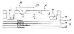
- FIGS. 3 and 4two embodiments of field effect transistors in accordance with the invention are illustrated in cross section.
- the transistorincludes a structure which can be similar to the structure described in application Ser. No. 11/132,619, supra.
- substrate 30can be silicon carbide
- buffer or nucleation layer 32can be AlGaN or GaN
- channel layer 34can be InAlGaN, GaN or AlGaN
- barrier layer 36can be a group III nitride.
- buffer layer 32 on the substrate 30provides an appropriate crystalline transition between the substrate 30 and the remainder of the device.
- Buffer layer 32may include one or more layers of InAlGaN.
- buffer layer 32may include GaN, AlN or AlGaN.
- Silicon carbidehas a much closer crystal lattice match to Group III nitrides than does sapphire (Al 2 O 3 ), which is a very common substrate material for Group III nitride devices. The closer lattice match may result in Group III nitride films of higher quality than those generally available on sapphire. Silicon carbide also has a very high thermal conductivity so that the total output power of Group III nitride devices on silicon carbide is, typically, not as limited by thermal dissipation of the substrate as in the case of the same devices formed on sapphire. Also, the availability of semi-insulating silicon carbide substrates may provide for device isolation and reduced parasitic capacitance. Exemplary HEMT structures are illustrated in U.S. Pat. Nos.
- semi-insulating silicon carbideis the preferred substrate material
- embodiments of the present inventionmay utilize any suitable substrate, such as sapphire, aluminum nitride, aluminum gallium nitride, gallium nitride, silicon, GaAs, LGO, ZnO, LAO, InP and the like.
- the substratemay be conductive, semi-insulating or highly resistive.
- an appropriate buffer layeralso may be formed.
- barrier layer 36Provided on barrier layer 36 is a first dielectric layer 38 with a second dielectric layer 40 on dielectric layer 38 .
- Contact holesare etched through layers 38 , 40 for a source contact 42 and a drain contact 44 .
- a preferential etchantcan be used to etch only dielectric 40 with a gate contact 46 formed on gate dielectric 38 .
- dielectric 38can be silicon oxide and dielectric 40 can be silicon nitride.
- the two dielectric layerscan be the same material which is deposited or formed at different times in the process to form two layers.
- Other known barrier layer materialscan be employed, also.
- gate contact 46can be extended over dielectric layer 40 towards the drain, as shown at 46 ′ to form a field plate extension.
- the field plate extension of the gate electrode towards the drain over the thicker dielectriccan be designed to shape the peak electric field with minimum impact on increased gate capacitance. The use of a field plate in other applications is known.
- FIG. 4illustrates in cross-section another embodiment of a field effect transistor in accordance with the invention.
- the substrate 30 and layers 32 - 36can be the same as in FIG. 3 .
- three dielectric layersare employed including layers 38 and 40 as in FIG. 3 along with a third dielectric layer 48 .
- the gate contact openingis etched through both dielectric layers 38 , 40 and then the third dielectric is deposited in the gate opening.
- Gate metallizationis then deposited on the stacked dielectric to form gate electrode 46 , which can have a shorter gate length, L G , and lower capacitance than other structures.
- dielectric 38has a thickness d 1
- dielectric 40has a thickness d 2
- dielectric 48has a thickness, d 3 .
- the thicknesses, d 1 , d 2 , and d 3are optimized to reliably support V GD , maintain frequency response, and minimize C gd and C gs .
- Gate length, L Gis tuned for the operational frequency of interest.
- dielectrics 38 and 40can be SiO 2 and SiN or the same material, as in FIG. 3
- dielectric layer 48can be SiO 2 .
- the top and bottom dielectricsshould be of higher bandgap than the middle dielectric.
- Novel use of this device in a switch-mode amplifierenables reliable operation because it avoids large detrimental forward gate current during the part of the cycle that the transistor is on.
Landscapes
- Engineering & Computer Science (AREA)
- Power Engineering (AREA)
- Junction Field-Effect Transistors (AREA)
- Amplifiers (AREA)
Abstract
Description
Claims (20)
Priority Applications (1)
| Application Number | Priority Date | Filing Date | Title |
|---|---|---|---|
| US12/474,570US7875914B2 (en) | 2005-07-21 | 2009-05-29 | Switch mode power amplifier using mis-HEMT with field plate extension |
Applications Claiming Priority (2)
| Application Number | Priority Date | Filing Date | Title |
|---|---|---|---|
| US11/187,171US7548112B2 (en) | 2005-07-21 | 2005-07-21 | Switch mode power amplifier using MIS-HEMT with field plate extension |
| US12/474,570US7875914B2 (en) | 2005-07-21 | 2009-05-29 | Switch mode power amplifier using mis-HEMT with field plate extension |
Related Parent Applications (1)
| Application Number | Title | Priority Date | Filing Date |
|---|---|---|---|
| US11/187,171ContinuationUS7548112B2 (en) | 2005-07-21 | 2005-07-21 | Switch mode power amplifier using MIS-HEMT with field plate extension |
Publications (2)
| Publication Number | Publication Date |
|---|---|
| US20090237160A1 US20090237160A1 (en) | 2009-09-24 |
| US7875914B2true US7875914B2 (en) | 2011-01-25 |
Family
ID=37678265
Family Applications (2)
| Application Number | Title | Priority Date | Filing Date |
|---|---|---|---|
| US11/187,171Active2026-07-11US7548112B2 (en) | 2005-07-21 | 2005-07-21 | Switch mode power amplifier using MIS-HEMT with field plate extension |
| US12/474,570Expired - LifetimeUS7875914B2 (en) | 2005-07-21 | 2009-05-29 | Switch mode power amplifier using mis-HEMT with field plate extension |
Family Applications Before (1)
| Application Number | Title | Priority Date | Filing Date |
|---|---|---|---|
| US11/187,171Active2026-07-11US7548112B2 (en) | 2005-07-21 | 2005-07-21 | Switch mode power amplifier using MIS-HEMT with field plate extension |
Country Status (7)
| Country | Link |
|---|---|
| US (2) | US7548112B2 (en) |
| EP (1) | EP1905096B1 (en) |
| JP (1) | JP2009514267A (en) |
| KR (1) | KR101343770B1 (en) |
| CA (1) | CA2611066C (en) |
| TW (1) | TWI416865B (en) |
| WO (1) | WO2007014036A2 (en) |
Cited By (41)
| Publication number | Priority date | Publication date | Assignee | Title |
|---|---|---|---|---|
| US20090072269A1 (en)* | 2007-09-17 | 2009-03-19 | Chang Soo Suh | Gallium nitride diodes and integrated components |
| US20090267078A1 (en)* | 2008-04-23 | 2009-10-29 | Transphorm Inc. | Enhancement Mode III-N HEMTs |
| US20100073067A1 (en)* | 2008-09-23 | 2010-03-25 | Transphorm Inc. | Inductive Load Power Switching Circuits |
| US20100289067A1 (en)* | 2009-05-14 | 2010-11-18 | Transphorm Inc. | High Voltage III-Nitride Semiconductor Devices |
| US20110049526A1 (en)* | 2009-08-28 | 2011-03-03 | Transphorm Inc. | Semiconductor Devices with Field Plates |
| US20110127541A1 (en)* | 2008-12-10 | 2011-06-02 | Transphorm Inc. | Semiconductor heterostructure diodes |
| US20110140172A1 (en)* | 2009-12-10 | 2011-06-16 | Transphorm Inc. | Reverse side engineered iii-nitride devices |
| US20110169549A1 (en)* | 2010-01-08 | 2011-07-14 | Transphorm Inc. | Electronic devices and components for high efficiency power circuits |
| US20110193619A1 (en)* | 2010-02-05 | 2011-08-11 | Transphorm Inc. | Semiconductor electronic components and circuits |
| US8455931B2 (en) | 2009-11-02 | 2013-06-04 | Transphorm Inc. | Package configurations for low EMI circuits |
| US8508281B2 (en) | 2008-02-12 | 2013-08-13 | Transphorm Inc. | Bridge circuits and their components |
| US8598937B2 (en) | 2011-10-07 | 2013-12-03 | Transphorm Inc. | High power semiconductor electronic components with increased reliability |
| US8643062B2 (en) | 2011-02-02 | 2014-02-04 | Transphorm Inc. | III-N device structures and methods |
| US8648643B2 (en) | 2012-02-24 | 2014-02-11 | Transphorm Inc. | Semiconductor power modules and devices |
| US8716141B2 (en) | 2011-03-04 | 2014-05-06 | Transphorm Inc. | Electrode configurations for semiconductor devices |
| US8742460B2 (en) | 2010-12-15 | 2014-06-03 | Transphorm Inc. | Transistors with isolation regions |
| US8772842B2 (en) | 2011-03-04 | 2014-07-08 | Transphorm, Inc. | Semiconductor diodes with low reverse bias currents |
| US8786327B2 (en) | 2011-02-28 | 2014-07-22 | Transphorm Inc. | Electronic components with reactive filters |
| US8803246B2 (en) | 2012-07-16 | 2014-08-12 | Transphorm Inc. | Semiconductor electronic components with integrated current limiters |
| US9041469B1 (en) | 2011-07-07 | 2015-05-26 | The United States Of America As Represented By The Administrator Of National Aeronautics And Space Administration | High-efficiency power module |
| US9059076B2 (en) | 2013-04-01 | 2015-06-16 | Transphorm Inc. | Gate drivers for circuits based on semiconductor devices |
| US9093366B2 (en) | 2012-04-09 | 2015-07-28 | Transphorm Inc. | N-polar III-nitride transistors |
| US9165766B2 (en) | 2012-02-03 | 2015-10-20 | Transphorm Inc. | Buffer layer structures suited for III-nitride devices with foreign substrates |
| US9171730B2 (en) | 2013-02-15 | 2015-10-27 | Transphorm Inc. | Electrodes for semiconductor devices and methods of forming the same |
| US9184275B2 (en) | 2012-06-27 | 2015-11-10 | Transphorm Inc. | Semiconductor devices with integrated hole collectors |
| US9209176B2 (en) | 2011-12-07 | 2015-12-08 | Transphorm Inc. | Semiconductor modules and methods of forming the same |
| US9224805B2 (en) | 2011-09-06 | 2015-12-29 | Transphorm Inc. | Semiconductor devices with guard rings |
| US9245993B2 (en) | 2013-03-15 | 2016-01-26 | Transphorm Inc. | Carbon doping semiconductor devices |
| US9257547B2 (en) | 2011-09-13 | 2016-02-09 | Transphorm Inc. | III-N device structures having a non-insulating substrate |
| US9318593B2 (en) | 2014-07-21 | 2016-04-19 | Transphorm Inc. | Forming enhancement mode III-nitride devices |
| US9443938B2 (en) | 2013-07-19 | 2016-09-13 | Transphorm Inc. | III-nitride transistor including a p-type depleting layer |
| US9536967B2 (en) | 2014-12-16 | 2017-01-03 | Transphorm Inc. | Recessed ohmic contacts in a III-N device |
| US9536966B2 (en) | 2014-12-16 | 2017-01-03 | Transphorm Inc. | Gate structures for III-N devices |
| US9537425B2 (en) | 2013-07-09 | 2017-01-03 | Transphorm Inc. | Multilevel inverters and their components |
| US9543940B2 (en) | 2014-07-03 | 2017-01-10 | Transphorm Inc. | Switching circuits having ferrite beads |
| US9590060B2 (en) | 2013-03-13 | 2017-03-07 | Transphorm Inc. | Enhancement-mode III-nitride devices |
| US9590494B1 (en) | 2014-07-17 | 2017-03-07 | Transphorm Inc. | Bridgeless power factor correction circuits |
| US10200030B2 (en) | 2015-03-13 | 2019-02-05 | Transphorm Inc. | Paralleling of switching devices for high power circuits |
| US10224401B2 (en) | 2016-05-31 | 2019-03-05 | Transphorm Inc. | III-nitride devices including a graded depleting layer |
| US10319648B2 (en) | 2017-04-17 | 2019-06-11 | Transphorm Inc. | Conditions for burn-in of high power semiconductors |
| US11322599B2 (en) | 2016-01-15 | 2022-05-03 | Transphorm Technology, Inc. | Enhancement mode III-nitride devices having an Al1-xSixO gate insulator |
Families Citing this family (98)
| Publication number | Priority date | Publication date | Assignee | Title |
|---|---|---|---|---|
| US7112860B2 (en) | 2003-03-03 | 2006-09-26 | Cree, Inc. | Integrated nitride-based acoustic wave devices and methods of fabricating integrated nitride-based acoustic wave devices |
| US7898047B2 (en)* | 2003-03-03 | 2011-03-01 | Samsung Electronics Co., Ltd. | Integrated nitride and silicon carbide-based devices and methods of fabricating integrated nitride-based devices |
| US9608102B2 (en)* | 2005-12-02 | 2017-03-28 | Infineon Technologies Americas Corp. | Gallium nitride material devices and associated methods |
| US7728402B2 (en) | 2006-08-01 | 2010-06-01 | Cree, Inc. | Semiconductor devices including schottky diodes with controlled breakdown |
| US8432012B2 (en) | 2006-08-01 | 2013-04-30 | Cree, Inc. | Semiconductor devices including schottky diodes having overlapping doped regions and methods of fabricating same |
| KR101529331B1 (en)* | 2006-08-17 | 2015-06-16 | 크리 인코포레이티드 | High power insulated gate bipolar transistors |
| US7973304B2 (en)* | 2007-02-06 | 2011-07-05 | International Rectifier Corporation | III-nitride semiconductor device |
| US8835987B2 (en) | 2007-02-27 | 2014-09-16 | Cree, Inc. | Insulated gate bipolar transistors including current suppressing layers |
| US7875537B2 (en)* | 2007-08-29 | 2011-01-25 | Cree, Inc. | High temperature ion implantation of nitride based HEMTs |
| EP2887402B1 (en)* | 2007-09-12 | 2019-06-12 | Transphorm Inc. | III-nitride bidirectional switches |
| US7915643B2 (en) | 2007-09-17 | 2011-03-29 | Transphorm Inc. | Enhancement mode gallium nitride power devices |
| US7800132B2 (en)* | 2007-10-25 | 2010-09-21 | Northrop Grumman Systems Corporation | High electron mobility transistor semiconductor device having field mitigating plate and fabrication method thereof |
| ATE463912T1 (en)* | 2007-11-12 | 2010-04-15 | Lucent Technologies Inc | RADIO FREQUENCY TRANSMITTER |
| US7632726B2 (en)* | 2007-12-07 | 2009-12-15 | Northrop Grumman Space & Mission Systems Corp. | Method for fabricating a nitride FET including passivation layers |
| US8431962B2 (en)* | 2007-12-07 | 2013-04-30 | Northrop Grumman Systems Corporation | Composite passivation process for nitride FET |
| US7750370B2 (en)* | 2007-12-20 | 2010-07-06 | Northrop Grumman Space & Mission Systems Corp. | High electron mobility transistor having self-aligned miniature field mitigating plate on a protective dielectric layer |
| US8232558B2 (en) | 2008-05-21 | 2012-07-31 | Cree, Inc. | Junction barrier Schottky diodes with current surge capability |
| RU2393624C1 (en)* | 2008-12-11 | 2010-06-27 | Александр Владимирович Баранов | Key power amplifier |
| US7884394B2 (en)* | 2009-02-09 | 2011-02-08 | Transphorm Inc. | III-nitride devices and circuits |
| RU2402149C1 (en)* | 2009-03-16 | 2010-10-20 | Александр Владимирович Баранов | Key power amplifier |
| US8754496B2 (en)* | 2009-04-14 | 2014-06-17 | Triquint Semiconductor, Inc. | Field effect transistor having a plurality of field plates |
| US8008977B2 (en)* | 2009-04-14 | 2011-08-30 | Triquint Semiconductor, Inc. | Field-plated transistor including feedback resistor |
| US8294507B2 (en) | 2009-05-08 | 2012-10-23 | Cree, Inc. | Wide bandgap bipolar turn-off thyristor having non-negative temperature coefficient and related control circuits |
| US8193848B2 (en) | 2009-06-02 | 2012-06-05 | Cree, Inc. | Power switching devices having controllable surge current capabilities |
| US8629509B2 (en) | 2009-06-02 | 2014-01-14 | Cree, Inc. | High voltage insulated gate bipolar transistors with minority carrier diverter |
| US8541787B2 (en) | 2009-07-15 | 2013-09-24 | Cree, Inc. | High breakdown voltage wide band-gap MOS-gated bipolar junction transistors with avalanche capability |
| US8354690B2 (en) | 2009-08-31 | 2013-01-15 | Cree, Inc. | Solid-state pinch off thyristor circuits |
| US9312343B2 (en)* | 2009-10-13 | 2016-04-12 | Cree, Inc. | Transistors with semiconductor interconnection layers and semiconductor channel layers of different semiconductor materials |
| JP5625336B2 (en)* | 2009-11-30 | 2014-11-19 | サンケン電気株式会社 | Semiconductor device |
| KR101226955B1 (en) | 2009-12-11 | 2013-01-28 | 한국전자통신연구원 | method for manufacturing Field Effect Transistor |
| JP2011135357A (en)* | 2009-12-24 | 2011-07-07 | Toyohashi Univ Of Technology | Switching circuit, distributed constant type switching circuit, and envelope signal amplifier |
| US8563372B2 (en)* | 2010-02-11 | 2013-10-22 | Cree, Inc. | Methods of forming contact structures including alternating metal and silicon layers and related devices |
| US9214352B2 (en) | 2010-02-11 | 2015-12-15 | Cree, Inc. | Ohmic contact to semiconductor device |
| US9548206B2 (en) | 2010-02-11 | 2017-01-17 | Cree, Inc. | Ohmic contact structure for group III nitride semiconductor device having improved surface morphology and well-defined edge features |
| US9117739B2 (en) | 2010-03-08 | 2015-08-25 | Cree, Inc. | Semiconductor devices with heterojunction barrier regions and methods of fabricating same |
| US8415671B2 (en) | 2010-04-16 | 2013-04-09 | Cree, Inc. | Wide band-gap MOSFETs having a heterojunction under gate trenches thereof and related methods of forming such devices |
| US8829999B2 (en) | 2010-05-20 | 2014-09-09 | Cree, Inc. | Low noise amplifiers including group III nitride based high electron mobility transistors |
| US8357571B2 (en)* | 2010-09-10 | 2013-01-22 | Cree, Inc. | Methods of forming semiconductor contacts |
| KR101775560B1 (en) | 2010-12-17 | 2017-09-07 | 한국전자통신연구원 | Field-Effect Transistor and Manufacturing Method Thereof |
| JP5638426B2 (en)* | 2011-03-07 | 2014-12-10 | 三菱電機株式会社 | Multistage amplifier |
| US9673283B2 (en) | 2011-05-06 | 2017-06-06 | Cree, Inc. | Power module for supporting high current densities |
| US9142662B2 (en) | 2011-05-06 | 2015-09-22 | Cree, Inc. | Field effect transistor devices with low source resistance |
| US9029945B2 (en) | 2011-05-06 | 2015-05-12 | Cree, Inc. | Field effect transistor devices with low source resistance |
| US8470652B1 (en) | 2011-05-11 | 2013-06-25 | Hrl Laboratories, Llc | Monolithic integration of group III nitride enhancement layers |
| US9373617B2 (en) | 2011-09-11 | 2016-06-21 | Cree, Inc. | High current, low switching loss SiC power module |
| US9640617B2 (en) | 2011-09-11 | 2017-05-02 | Cree, Inc. | High performance power module |
| US8664665B2 (en) | 2011-09-11 | 2014-03-04 | Cree, Inc. | Schottky diode employing recesses for elements of junction barrier array |
| US8680587B2 (en) | 2011-09-11 | 2014-03-25 | Cree, Inc. | Schottky diode |
| US8618582B2 (en) | 2011-09-11 | 2013-12-31 | Cree, Inc. | Edge termination structure employing recesses for edge termination elements |
| JP2013074069A (en) | 2011-09-27 | 2013-04-22 | Fujitsu Ltd | Semiconductor device and manufacturing method of semiconductor device |
| US9392681B2 (en) | 2012-08-03 | 2016-07-12 | Schlumberger Technology Corporation | Borehole power amplifier |
| US20140035588A1 (en)* | 2012-08-03 | 2014-02-06 | Schlumberger Technology Corporation | Borehole particle accelerator |
| JP6085442B2 (en) | 2012-09-28 | 2017-02-22 | トランスフォーム・ジャパン株式会社 | Compound semiconductor device and manufacturing method thereof |
| KR101923972B1 (en) | 2012-12-18 | 2018-11-30 | 한국전자통신연구원 | Transistor and Method of Fabricating the Same |
| US9343561B2 (en) | 2013-03-13 | 2016-05-17 | Cree, Inc. | Semiconductor device with self-aligned ohmic contacts |
| US8969927B2 (en) | 2013-03-13 | 2015-03-03 | Cree, Inc. | Gate contact for a semiconductor device and methods of fabrication thereof |
| US9018056B2 (en)* | 2013-03-15 | 2015-04-28 | The United States Of America, As Represented By The Secretary Of The Navy | Complementary field effect transistors using gallium polar and nitrogen polar III-nitride material |
| ES2743052T3 (en)* | 2013-04-09 | 2020-02-18 | Otis Elevator Co | Drive unit architecture employing gallium nitride switches |
| US9755059B2 (en) | 2013-06-09 | 2017-09-05 | Cree, Inc. | Cascode structures with GaN cap layers |
| US9130026B2 (en)* | 2013-09-03 | 2015-09-08 | Taiwan Semiconductor Manufacturing Co., Ltd. | Crystalline layer for passivation of III-N surface |
| JP2015056457A (en)* | 2013-09-10 | 2015-03-23 | 株式会社東芝 | Semiconductor device |
| CN104810264B (en)* | 2014-01-26 | 2017-12-01 | 国家电网公司 | A kind of SiC terminal structure preparation methods based on ONO structure |
| US9565642B2 (en) | 2014-04-11 | 2017-02-07 | Cree, Inc. | GaN amplifier for WiFi applications |
| US9425301B2 (en) | 2014-04-30 | 2016-08-23 | Taiwan Semiconductor Manufacturing Co., Ltd. | Sidewall passivation for HEMT devices |
| KR102135163B1 (en) | 2014-06-26 | 2020-07-20 | 한국전자통신연구원 | Semiconductor device and fabrication method thereof |
| US9871067B2 (en)* | 2015-11-17 | 2018-01-16 | Taiwan Semiconductor Manufacturing Co., Ltd. | Infrared image sensor component |
| KR102208076B1 (en) | 2016-02-12 | 2021-01-28 | 한국전자통신연구원 | High electron mobility transistor and fabrication method thereof |
| CN105895705B (en)* | 2016-05-27 | 2018-11-27 | 中国电子科技集团公司第五十五研究所 | A kind of " Γ " type grid structure of radio frequency LDMOS and preparation method thereof |
| JP2017208556A (en)* | 2017-06-27 | 2017-11-24 | 株式会社東芝 | Semiconductor device |
| US10608102B2 (en) | 2017-09-29 | 2020-03-31 | Electronics And Telecommunications Research Institute | Semiconductor device having a drain electrode contacting an epi material inside a through-hole and method of manufacturing the same |
| US10777638B1 (en)* | 2018-01-04 | 2020-09-15 | Synopsys, Inc. | Constricted junctionless FinFET/nanowire/nanosheet device having cascode portion |
| CN109534278B (en)* | 2018-11-01 | 2020-12-15 | 中国科学院半导体研究所 | Structure of Heterogeneous Integration of Acoustic Filter and HEMT and Preparation Method thereof |
| US10923585B2 (en) | 2019-06-13 | 2021-02-16 | Cree, Inc. | High electron mobility transistors having improved contact spacing and/or improved contact vias |
| US10971612B2 (en) | 2019-06-13 | 2021-04-06 | Cree, Inc. | High electron mobility transistors and power amplifiers including said transistors having improved performance and reliability |
| US11239802B2 (en)* | 2019-10-02 | 2022-02-01 | Wolfspeed, Inc. | Radio frequency transistor amplifiers having engineered instrinsic capacitances for improved performance |
| US11670605B2 (en) | 2020-04-03 | 2023-06-06 | Wolfspeed, Inc. | RF amplifier devices including interconnect structures and methods of manufacturing |
| US12166003B2 (en) | 2020-04-03 | 2024-12-10 | Macom Technology Solutions Holdings, Inc. | RF amplifier devices including top side contacts and methods of manufacturing |
| US11356070B2 (en) | 2020-06-01 | 2022-06-07 | Wolfspeed, Inc. | RF amplifiers having shielded transmission line structures |
| US11837457B2 (en) | 2020-09-11 | 2023-12-05 | Wolfspeed, Inc. | Packaging for RF transistor amplifiers |
| US11769768B2 (en) | 2020-06-01 | 2023-09-26 | Wolfspeed, Inc. | Methods for pillar connection on frontside and passive device integration on backside of die |
| US11228287B2 (en) | 2020-06-17 | 2022-01-18 | Cree, Inc. | Multi-stage decoupling networks integrated with on-package impedance matching networks for RF power amplifiers |
| US11533025B2 (en) | 2020-06-18 | 2022-12-20 | Wolfspeed, Inc. | Integrated doherty amplifier with added isolation between the carrier and the peaking transistors |
| US11581859B2 (en) | 2020-06-26 | 2023-02-14 | Wolfspeed, Inc. | Radio frequency (RF) transistor amplifier packages with improved isolation and lead configurations |
| US11887945B2 (en) | 2020-09-30 | 2024-01-30 | Wolfspeed, Inc. | Semiconductor device with isolation and/or protection structures |
| US12272660B2 (en) | 2020-10-30 | 2025-04-08 | Wolfspeed, Inc. | Transistor packages with improved die attach |
| US12100630B2 (en) | 2020-11-13 | 2024-09-24 | Macom Technology Solutions Holdings, Inc. | Packaged RF power device with PCB routing outside protective member |
| US12009417B2 (en) | 2021-05-20 | 2024-06-11 | Macom Technology Solutions Holdings, Inc. | High electron mobility transistors having improved performance |
| US12015075B2 (en) | 2021-05-20 | 2024-06-18 | Macom Technology Solutions Holdings, Inc. | Methods of manufacturing high electron mobility transistors having a modified interface region |
| US11842937B2 (en) | 2021-07-30 | 2023-12-12 | Wolfspeed, Inc. | Encapsulation stack for improved humidity performance and related fabrication methods |
| US20230075505A1 (en) | 2021-09-03 | 2023-03-09 | Wolfspeed, Inc. | Metal pillar connection topologies for heterogeneous packaging |
| US12218202B2 (en) | 2021-09-16 | 2025-02-04 | Wolfspeed, Inc. | Semiconductor device incorporating a substrate recess |
| TWI799127B (en)* | 2022-02-09 | 2023-04-11 | 新唐科技股份有限公司 | High electron mobility semiconductor structure and high electron mobility semiconductor device |
| US20240106397A1 (en) | 2022-09-23 | 2024-03-28 | Wolfspeed, Inc. | Transistor amplifier with pcb routing and surface mounted transistor die |
| US20240105823A1 (en) | 2022-09-23 | 2024-03-28 | Wolfspeed, Inc. | Barrier Structure for Dispersion Reduction in Transistor Devices |
| US20240105824A1 (en) | 2022-09-23 | 2024-03-28 | Wolfspeed, Inc. | Barrier Structure for Sub-100 Nanometer Gate Length Devices |
| US20240266426A1 (en) | 2023-02-03 | 2024-08-08 | Wolfspeed, Inc. | Semiconductor Structure for Improved Radio Frequency Thermal Management |
| WO2024258898A1 (en) | 2023-06-14 | 2024-12-19 | Wolfspeed, Inc. | Rf amplifier package and manufacturing method thereof |
| US20250194190A1 (en) | 2023-12-12 | 2025-06-12 | Wolfspeed, Inc. | Substrates for Power Semiconductor Devices |
Citations (10)
| Publication number | Priority date | Publication date | Assignee | Title |
|---|---|---|---|---|
| US5187580A (en)* | 1991-02-04 | 1993-02-16 | Advanced Energy Industries, Inc. | High power switch-mode radio frequency amplifier method and apparatus |
| US5939941A (en)* | 1997-09-25 | 1999-08-17 | Motorola, Inc. | High efficiency power amplifier using HITFET driver circuit |
| US20030020092A1 (en) | 2001-07-24 | 2003-01-30 | Primit Parikh | Insulating gate AlGaN/GaN HEMT |
| US6724255B2 (en)* | 2000-10-10 | 2004-04-20 | California Institute Of Technology | Class E/F switching power amplifiers |
| US20040137673A1 (en)* | 2003-01-09 | 2004-07-15 | Matthias Passlack | Enhancement mode metal-oxide-semiconductor field effect transistor and method for forming the same |
| US20050051796A1 (en)* | 2003-09-09 | 2005-03-10 | Cree, Inc. | Wide bandgap transistor devices with field plates |
| US20050051800A1 (en) | 2003-09-09 | 2005-03-10 | Cree, Inc. | Cascode amplifier structures including wide bandgap field effect transistor with field plates |
| US20050245037A1 (en)* | 2004-05-03 | 2005-11-03 | Dongbuanam Semiconductor Inc. | Method for fabricating flash memory device |
| US7236053B2 (en)* | 2004-12-31 | 2007-06-26 | Cree, Inc. | High efficiency switch-mode power amplifier |
| EP1843390A1 (en) | 2005-01-25 | 2007-10-10 | Fujitsu Limited | Semiconductor device provided with mis structure and method for manufacturing the same |
Family Cites Families (7)
| Publication number | Priority date | Publication date | Assignee | Title |
|---|---|---|---|---|
| JPH04207803A (en)* | 1990-11-30 | 1992-07-29 | Toshiba Corp | Amplifier |
| US6232841B1 (en)* | 1999-07-01 | 2001-05-15 | Rockwell Science Center, Llc | Integrated tunable high efficiency power amplifier |
| US6549071B1 (en)* | 2000-09-12 | 2003-04-15 | Silicon Laboratories, Inc. | Power amplifier circuitry and method using an inductance coupled to power amplifier switching devices |
| TW563293B (en)* | 2002-04-29 | 2003-11-21 | Ok-Sang Jin | Signal amplifying method, signal amplifier and devices related therewith |
| JP3499235B1 (en)* | 2002-08-28 | 2004-02-23 | 株式会社フライングモール | Switching circuit and digital power amplifier |
| JP4385205B2 (en)* | 2002-12-16 | 2009-12-16 | 日本電気株式会社 | Field effect transistor |
| US7649215B2 (en)* | 2003-12-05 | 2010-01-19 | International Rectifier Corporation | III-nitride device passivation and method |
- 2005
- 2005-07-21USUS11/187,171patent/US7548112B2/enactiveActive
- 2006
- 2006-07-19JPJP2008522992Apatent/JP2009514267A/enactivePending
- 2006-07-19CACA2611066Apatent/CA2611066C/enactiveActive
- 2006-07-19EPEP06788110.2Apatent/EP1905096B1/enactiveActive
- 2006-07-19WOPCT/US2006/028370patent/WO2007014036A2/enactiveApplication Filing
- 2006-07-21TWTW095126799Apatent/TWI416865B/ennot_activeIP Right Cessation
- 2007
- 2007-12-06KRKR1020077028563Apatent/KR101343770B1/ennot_activeExpired - Fee Related
- 2009
- 2009-05-29USUS12/474,570patent/US7875914B2/ennot_activeExpired - Lifetime
Patent Citations (10)
| Publication number | Priority date | Publication date | Assignee | Title |
|---|---|---|---|---|
| US5187580A (en)* | 1991-02-04 | 1993-02-16 | Advanced Energy Industries, Inc. | High power switch-mode radio frequency amplifier method and apparatus |
| US5939941A (en)* | 1997-09-25 | 1999-08-17 | Motorola, Inc. | High efficiency power amplifier using HITFET driver circuit |
| US6724255B2 (en)* | 2000-10-10 | 2004-04-20 | California Institute Of Technology | Class E/F switching power amplifiers |
| US20030020092A1 (en) | 2001-07-24 | 2003-01-30 | Primit Parikh | Insulating gate AlGaN/GaN HEMT |
| US20040137673A1 (en)* | 2003-01-09 | 2004-07-15 | Matthias Passlack | Enhancement mode metal-oxide-semiconductor field effect transistor and method for forming the same |
| US20050051796A1 (en)* | 2003-09-09 | 2005-03-10 | Cree, Inc. | Wide bandgap transistor devices with field plates |
| US20050051800A1 (en) | 2003-09-09 | 2005-03-10 | Cree, Inc. | Cascode amplifier structures including wide bandgap field effect transistor with field plates |
| US20050245037A1 (en)* | 2004-05-03 | 2005-11-03 | Dongbuanam Semiconductor Inc. | Method for fabricating flash memory device |
| US7236053B2 (en)* | 2004-12-31 | 2007-06-26 | Cree, Inc. | High efficiency switch-mode power amplifier |
| EP1843390A1 (en) | 2005-01-25 | 2007-10-10 | Fujitsu Limited | Semiconductor device provided with mis structure and method for manufacturing the same |
Non-Patent Citations (8)
| Title |
|---|
| International Search Report and Written Opinion; PCT/US06/28370; Jan. 28, 2008. |
| Office Action corresponding to European Application No. 06788110.2 mailed Sep. 9, 2009, (9 pages). |
| U.S. Appl. No. 10/958,945, filed Oct. 4, 2004. |
| U.S. Appl. No. 10/958,970, filed Oct. 4, 2004. |
| U.S. Appl. No. 10/976,422, filed Oct. 29, 2004. |
| U.S. Appl. No. 11/078,265, filed Mar. 11, 2005. |
| U.S. Appl. No. 11/132,619, filed May 18, 2005. |
| Wang et al. "High Temperature Performance and Low Frequency Noise Characteristics of AlGaN/GaN/AlGaN Double Heterostructure Metal-Oxide-Semiconductor Heterostructure Field-Effect-Transistors with Photochemical Vapor Deposition SiO2 Layer" Japanese Journal of Applied Physics 44(4B):2458-2461 (2005). |
Cited By (105)
| Publication number | Priority date | Publication date | Assignee | Title |
|---|---|---|---|---|
| US20090072269A1 (en)* | 2007-09-17 | 2009-03-19 | Chang Soo Suh | Gallium nitride diodes and integrated components |
| US8912839B2 (en) | 2008-02-12 | 2014-12-16 | Transphorm Inc. | Bridge circuits and their components |
| US8508281B2 (en) | 2008-02-12 | 2013-08-13 | Transphorm Inc. | Bridge circuits and their components |
| US9899998B2 (en) | 2008-02-12 | 2018-02-20 | Transphorm Inc. | Bridge circuits and their components |
| US20090267078A1 (en)* | 2008-04-23 | 2009-10-29 | Transphorm Inc. | Enhancement Mode III-N HEMTs |
| US8841702B2 (en) | 2008-04-23 | 2014-09-23 | Transphorm Inc. | Enhancement mode III-N HEMTs |
| US9437708B2 (en) | 2008-04-23 | 2016-09-06 | Transphorm Inc. | Enhancement mode III-N HEMTs |
| US8519438B2 (en) | 2008-04-23 | 2013-08-27 | Transphorm Inc. | Enhancement mode III-N HEMTs |
| US9941399B2 (en) | 2008-04-23 | 2018-04-10 | Transphorm Inc. | Enhancement mode III-N HEMTs |
| US9196716B2 (en) | 2008-04-23 | 2015-11-24 | Transphorm Inc. | Enhancement mode III-N HEMTs |
| US8289065B2 (en) | 2008-09-23 | 2012-10-16 | Transphorm Inc. | Inductive load power switching circuits |
| US8493129B2 (en) | 2008-09-23 | 2013-07-23 | Transphorm Inc. | Inductive load power switching circuits |
| US9690314B2 (en) | 2008-09-23 | 2017-06-27 | Transphorm Inc. | Inductive load power switching circuits |
| US8531232B2 (en) | 2008-09-23 | 2013-09-10 | Transphorm Inc. | Inductive load power switching circuits |
| US20100073067A1 (en)* | 2008-09-23 | 2010-03-25 | Transphorm Inc. | Inductive Load Power Switching Circuits |
| US8816751B2 (en) | 2008-09-23 | 2014-08-26 | Transphorm Inc. | Inductive load power switching circuits |
| US8237198B2 (en) | 2008-12-10 | 2012-08-07 | Transphorm Inc. | Semiconductor heterostructure diodes |
| US20110127541A1 (en)* | 2008-12-10 | 2011-06-02 | Transphorm Inc. | Semiconductor heterostructure diodes |
| US8541818B2 (en) | 2008-12-10 | 2013-09-24 | Transphorm Inc. | Semiconductor heterostructure diodes |
| US9041065B2 (en) | 2008-12-10 | 2015-05-26 | Transphorm Inc. | Semiconductor heterostructure diodes |
| US8742459B2 (en) | 2009-05-14 | 2014-06-03 | Transphorm Inc. | High voltage III-nitride semiconductor devices |
| US9293561B2 (en) | 2009-05-14 | 2016-03-22 | Transphorm Inc. | High voltage III-nitride semiconductor devices |
| US20100289067A1 (en)* | 2009-05-14 | 2010-11-18 | Transphorm Inc. | High Voltage III-Nitride Semiconductor Devices |
| US9831315B2 (en) | 2009-08-28 | 2017-11-28 | Transphorm Inc. | Semiconductor devices with field plates |
| US20110049526A1 (en)* | 2009-08-28 | 2011-03-03 | Transphorm Inc. | Semiconductor Devices with Field Plates |
| US8692294B2 (en) | 2009-08-28 | 2014-04-08 | Transphorm Inc. | Semiconductor devices with field plates |
| US9111961B2 (en) | 2009-08-28 | 2015-08-18 | Transphorm Inc. | Semiconductor devices with field plates |
| US8390000B2 (en) | 2009-08-28 | 2013-03-05 | Transphorm Inc. | Semiconductor devices with field plates |
| US9373699B2 (en) | 2009-08-28 | 2016-06-21 | Transphorm Inc. | Semiconductor devices with field plates |
| US8890314B2 (en) | 2009-11-02 | 2014-11-18 | Transphorm, Inc. | Package configurations for low EMI circuits |
| US9190295B2 (en) | 2009-11-02 | 2015-11-17 | Transphorm Inc. | Package configurations for low EMI circuits |
| US8455931B2 (en) | 2009-11-02 | 2013-06-04 | Transphorm Inc. | Package configurations for low EMI circuits |
| US8592974B2 (en) | 2009-11-02 | 2013-11-26 | Transphorm Inc. | Package configurations for low EMI circuits |
| US10199217B2 (en) | 2009-12-10 | 2019-02-05 | Transphorm Inc. | Methods of forming reverse side engineered III-nitride devices |
| US9496137B2 (en) | 2009-12-10 | 2016-11-15 | Transphorm Inc. | Methods of forming reverse side engineered III-nitride devices |
| US20110140172A1 (en)* | 2009-12-10 | 2011-06-16 | Transphorm Inc. | Reverse side engineered iii-nitride devices |
| US8389977B2 (en) | 2009-12-10 | 2013-03-05 | Transphorm Inc. | Reverse side engineered III-nitride devices |
| US9401341B2 (en) | 2010-01-08 | 2016-07-26 | Transphorm Inc. | Electronic devices and components for high efficiency power circuits |
| US8816497B2 (en) | 2010-01-08 | 2014-08-26 | Transphorm Inc. | Electronic devices and components for high efficiency power circuits |
| US20110169549A1 (en)* | 2010-01-08 | 2011-07-14 | Transphorm Inc. | Electronic devices and components for high efficiency power circuits |
| US8624662B2 (en) | 2010-02-05 | 2014-01-07 | Transphorm Inc. | Semiconductor electronic components and circuits |
| US9293458B2 (en) | 2010-02-05 | 2016-03-22 | Transphorm Inc. | Semiconductor electronic components and circuits |
| US20110193619A1 (en)* | 2010-02-05 | 2011-08-11 | Transphorm Inc. | Semiconductor electronic components and circuits |
| US8742460B2 (en) | 2010-12-15 | 2014-06-03 | Transphorm Inc. | Transistors with isolation regions |
| US9437707B2 (en) | 2010-12-15 | 2016-09-06 | Transphorm Inc. | Transistors with isolation regions |
| US9147760B2 (en) | 2010-12-15 | 2015-09-29 | Transphorm Inc. | Transistors with isolation regions |
| US9224671B2 (en) | 2011-02-02 | 2015-12-29 | Transphorm Inc. | III-N device structures and methods |
| US8643062B2 (en) | 2011-02-02 | 2014-02-04 | Transphorm Inc. | III-N device structures and methods |
| US8895421B2 (en) | 2011-02-02 | 2014-11-25 | Transphorm Inc. | III-N device structures and methods |
| US8786327B2 (en) | 2011-02-28 | 2014-07-22 | Transphorm Inc. | Electronic components with reactive filters |
| US9041435B2 (en) | 2011-02-28 | 2015-05-26 | Transphorm Inc. | Method of forming electronic components with reactive filters |
| US9142659B2 (en) | 2011-03-04 | 2015-09-22 | Transphorm Inc. | Electrode configurations for semiconductor devices |
| US8895423B2 (en) | 2011-03-04 | 2014-11-25 | Transphorm Inc. | Method for making semiconductor diodes with low reverse bias currents |
| US8772842B2 (en) | 2011-03-04 | 2014-07-08 | Transphorm, Inc. | Semiconductor diodes with low reverse bias currents |
| US8716141B2 (en) | 2011-03-04 | 2014-05-06 | Transphorm Inc. | Electrode configurations for semiconductor devices |
| US9041469B1 (en) | 2011-07-07 | 2015-05-26 | The United States Of America As Represented By The Administrator Of National Aeronautics And Space Administration | High-efficiency power module |
| US9224805B2 (en) | 2011-09-06 | 2015-12-29 | Transphorm Inc. | Semiconductor devices with guard rings |
| US9257547B2 (en) | 2011-09-13 | 2016-02-09 | Transphorm Inc. | III-N device structures having a non-insulating substrate |
| US8860495B2 (en) | 2011-10-07 | 2014-10-14 | Transphorm Inc. | Method of forming electronic components with increased reliability |
| US9171836B2 (en) | 2011-10-07 | 2015-10-27 | Transphorm Inc. | Method of forming electronic components with increased reliability |
| US8598937B2 (en) | 2011-10-07 | 2013-12-03 | Transphorm Inc. | High power semiconductor electronic components with increased reliability |
| US9209176B2 (en) | 2011-12-07 | 2015-12-08 | Transphorm Inc. | Semiconductor modules and methods of forming the same |
| US9818686B2 (en) | 2011-12-07 | 2017-11-14 | Transphorm Inc. | Semiconductor modules and methods of forming the same |
| US9685323B2 (en) | 2012-02-03 | 2017-06-20 | Transphorm Inc. | Buffer layer structures suited for III-nitride devices with foreign substrates |
| US9165766B2 (en) | 2012-02-03 | 2015-10-20 | Transphorm Inc. | Buffer layer structures suited for III-nitride devices with foreign substrates |
| US9224721B2 (en) | 2012-02-24 | 2015-12-29 | Transphorm Inc. | Semiconductor power modules and devices |
| US8952750B2 (en) | 2012-02-24 | 2015-02-10 | Transphorm Inc. | Semiconductor power modules and devices |
| US9741702B2 (en) | 2012-02-24 | 2017-08-22 | Transphorm Inc. | Semiconductor power modules and devices |
| US8648643B2 (en) | 2012-02-24 | 2014-02-11 | Transphorm Inc. | Semiconductor power modules and devices |
| US9093366B2 (en) | 2012-04-09 | 2015-07-28 | Transphorm Inc. | N-polar III-nitride transistors |
| US9490324B2 (en) | 2012-04-09 | 2016-11-08 | Transphorm Inc. | N-polar III-nitride transistors |
| US9184275B2 (en) | 2012-06-27 | 2015-11-10 | Transphorm Inc. | Semiconductor devices with integrated hole collectors |
| US9634100B2 (en) | 2012-06-27 | 2017-04-25 | Transphorm Inc. | Semiconductor devices with integrated hole collectors |
| US8803246B2 (en) | 2012-07-16 | 2014-08-12 | Transphorm Inc. | Semiconductor electronic components with integrated current limiters |
| US9443849B2 (en) | 2012-07-16 | 2016-09-13 | Transphorm Inc. | Semiconductor electronic components with integrated current limiters |
| US9171910B2 (en) | 2012-07-16 | 2015-10-27 | Transphorm Inc. | Semiconductor electronic components with integrated current limiters |
| US9171730B2 (en) | 2013-02-15 | 2015-10-27 | Transphorm Inc. | Electrodes for semiconductor devices and methods of forming the same |
| US9520491B2 (en) | 2013-02-15 | 2016-12-13 | Transphorm Inc. | Electrodes for semiconductor devices and methods of forming the same |
| US9590060B2 (en) | 2013-03-13 | 2017-03-07 | Transphorm Inc. | Enhancement-mode III-nitride devices |
| US10535763B2 (en) | 2013-03-13 | 2020-01-14 | Transphorm Inc. | Enhancement-mode III-nitride devices |
| US10043898B2 (en) | 2013-03-13 | 2018-08-07 | Transphorm Inc. | Enhancement-mode III-nitride devices |
| US9245993B2 (en) | 2013-03-15 | 2016-01-26 | Transphorm Inc. | Carbon doping semiconductor devices |
| US9865719B2 (en) | 2013-03-15 | 2018-01-09 | Transphorm Inc. | Carbon doping semiconductor devices |
| US9245992B2 (en) | 2013-03-15 | 2016-01-26 | Transphorm Inc. | Carbon doping semiconductor devices |
| US9059076B2 (en) | 2013-04-01 | 2015-06-16 | Transphorm Inc. | Gate drivers for circuits based on semiconductor devices |
| US9362903B2 (en) | 2013-04-01 | 2016-06-07 | Transphorm Inc. | Gate drivers for circuits based on semiconductor devices |
| US9537425B2 (en) | 2013-07-09 | 2017-01-03 | Transphorm Inc. | Multilevel inverters and their components |
| US9842922B2 (en) | 2013-07-19 | 2017-12-12 | Transphorm Inc. | III-nitride transistor including a p-type depleting layer |
| US9443938B2 (en) | 2013-07-19 | 2016-09-13 | Transphorm Inc. | III-nitride transistor including a p-type depleting layer |
| US10043896B2 (en) | 2013-07-19 | 2018-08-07 | Transphorm Inc. | III-Nitride transistor including a III-N depleting layer |
| US9660640B2 (en) | 2014-07-03 | 2017-05-23 | Transphorm Inc. | Switching circuits having ferrite beads |
| US9543940B2 (en) | 2014-07-03 | 2017-01-10 | Transphorm Inc. | Switching circuits having ferrite beads |
| US9991884B2 (en) | 2014-07-03 | 2018-06-05 | Transphorm Inc. | Switching circuits having ferrite beads |
| US9590494B1 (en) | 2014-07-17 | 2017-03-07 | Transphorm Inc. | Bridgeless power factor correction circuits |
| US10063138B1 (en) | 2014-07-17 | 2018-08-28 | Transphorm Inc. | Bridgeless power factor correction circuits |
| US9935190B2 (en) | 2014-07-21 | 2018-04-03 | Transphorm Inc. | Forming enhancement mode III-nitride devices |
| US9318593B2 (en) | 2014-07-21 | 2016-04-19 | Transphorm Inc. | Forming enhancement mode III-nitride devices |
| US9536966B2 (en) | 2014-12-16 | 2017-01-03 | Transphorm Inc. | Gate structures for III-N devices |
| US9536967B2 (en) | 2014-12-16 | 2017-01-03 | Transphorm Inc. | Recessed ohmic contacts in a III-N device |
| US10200030B2 (en) | 2015-03-13 | 2019-02-05 | Transphorm Inc. | Paralleling of switching devices for high power circuits |
| US11322599B2 (en) | 2016-01-15 | 2022-05-03 | Transphorm Technology, Inc. | Enhancement mode III-nitride devices having an Al1-xSixO gate insulator |
| US10224401B2 (en) | 2016-05-31 | 2019-03-05 | Transphorm Inc. | III-nitride devices including a graded depleting layer |
| US10629681B2 (en) | 2016-05-31 | 2020-04-21 | Transphorm Technology, Inc. | III-nitride devices including a graded depleting layer |
| US11121216B2 (en) | 2016-05-31 | 2021-09-14 | Transphorm Technology, Inc. | III-nitride devices including a graded depleting layer |
| US10319648B2 (en) | 2017-04-17 | 2019-06-11 | Transphorm Inc. | Conditions for burn-in of high power semiconductors |
Also Published As
| Publication number | Publication date |
|---|---|
| CA2611066C (en) | 2016-08-30 |
| TWI416865B (en) | 2013-11-21 |
| US20070018210A1 (en) | 2007-01-25 |
| EP1905096A2 (en) | 2008-04-02 |
| US20090237160A1 (en) | 2009-09-24 |
| TW200713800A (en) | 2007-04-01 |
| JP2009514267A (en) | 2009-04-02 |
| EP1905096B1 (en) | 2018-02-28 |
| WO2007014036A2 (en) | 2007-02-01 |
| CA2611066A1 (en) | 2007-02-01 |
| KR20080036002A (en) | 2008-04-24 |
| KR101343770B1 (en) | 2013-12-19 |
| WO2007014036A3 (en) | 2009-04-02 |
| EP1905096A4 (en) | 2009-10-21 |
| US7548112B2 (en) | 2009-06-16 |
Similar Documents
| Publication | Publication Date | Title |
|---|---|---|
| US7875914B2 (en) | Switch mode power amplifier using mis-HEMT with field plate extension | |
| US8829999B2 (en) | Low noise amplifiers including group III nitride based high electron mobility transistors | |
| US7518451B2 (en) | High efficiency switch-mode power amplifier | |
| US7388236B2 (en) | High efficiency and/or high power density wide bandgap transistors | |
| US7126426B2 (en) | Cascode amplifier structures including wide bandgap field effect transistor with field plates | |
| US12402348B2 (en) | Field effect transistor with selective channel layer doping | |
| Wu et al. | 3-9-GHz GaN-based microwave power amplifiers with LCR broad-band matching | |
| Chen et al. | Dual-gate AlGaN/GaN modulation-doped field-effect transistors with cut-off frequencies f T> 60 GHz | |
| Shealy et al. | Gallium nitride (GaN) HEMT's: progress and potential for commercial applications | |
| Peng et al. | 14.2 W/mm internally-matched AlGaN/GaN HEMT for X-band applications | |
| Sheppard et al. | High-Efficiency Amplifiers Using AlGaN/GaN HEMTs on SiC | |
| US20240072732A1 (en) | Transistor die including matching circuit | |
| US7795672B2 (en) | Profiled gate field effect transistor with enhanced high harmonic gain | |
| Tsurumi et al. | Gan transistors for power switching and high frequency applications | |
| Freitag et al. | Wideband 3 and 10 watt class e X-band GaN power MMICs with up to 75% power-added efficiency | |
| Mizuno et al. | A 5.9 GHz–8.5 GHz 20 Watts GaN HEMT |
Legal Events
| Date | Code | Title | Description |
|---|---|---|---|
| STCF | Information on status: patent grant | Free format text:PATENTED CASE | |
| FPAY | Fee payment | Year of fee payment:4 | |
| MAFP | Maintenance fee payment | Free format text:PAYMENT OF MAINTENANCE FEE, 8TH YEAR, LARGE ENTITY (ORIGINAL EVENT CODE: M1552) Year of fee payment:8 | |
| MAFP | Maintenance fee payment | Free format text:PAYMENT OF MAINTENANCE FEE, 12TH YEAR, LARGE ENTITY (ORIGINAL EVENT CODE: M1553); ENTITY STATUS OF PATENT OWNER: LARGE ENTITY Year of fee payment:12 | |
| AS | Assignment | Owner name:WOLFSPEED, INC., NORTH CAROLINA Free format text:CHANGE OF NAME;ASSIGNOR:CREE, INC.;REEL/FRAME:064615/0365 Effective date:20211001 | |
| AS | Assignment | Owner name:CREE, INC., NORTH CAROLINA Free format text:ASSIGNMENT OF ASSIGNORS INTEREST;ASSIGNOR:SHEPPARD, SCOTT;REEL/FRAME:064674/0634 Effective date:20050712 | |
| AS | Assignment | Owner name:MACOM TECHNOLOGY SOLUTIONS HOLDINGS, INC., MASSACHUSETTS Free format text:ASSIGNMENT OF ASSIGNORS INTEREST;ASSIGNOR:WOLFSPEED, INC.;REEL/FRAME:066236/0086 Effective date:20231206 |