US7874726B2 - Thermocouple - Google Patents
ThermocoupleDownload PDFInfo
- Publication number
- US7874726B2 US7874726B2US12/121,085US12108508AUS7874726B2US 7874726 B2US7874726 B2US 7874726B2US 12108508 AUS12108508 AUS 12108508AUS 7874726 B2US7874726 B2US 7874726B2
- Authority
- US
- United States
- Prior art keywords
- wires
- support tube
- cap
- thermocouple
- pair
- Prior art date
- Legal status (The legal status is an assumption and is not a legal conclusion. Google has not performed a legal analysis and makes no representation as to the accuracy of the status listed.)
- Active, expires
Links
- 230000008602contractionEffects0.000claimsabstractdescription10
- 229910052751metalInorganic materials0.000claimsabstractdescription7
- 239000002184metalSubstances0.000claimsabstractdescription7
- 150000002739metalsChemical class0.000claimsabstractdescription6
- 230000001681protective effectEffects0.000claimsdescription6
- 230000007423decreaseEffects0.000claimsdescription3
- 230000004044responseEffects0.000claimsdescription3
- 239000000758substrateSubstances0.000description40
- 238000006243chemical reactionMethods0.000description17
- 238000010438heat treatmentMethods0.000description13
- 238000012545processingMethods0.000description12
- 238000005229chemical vapour depositionMethods0.000description10
- 239000000919ceramicSubstances0.000description9
- 238000000034methodMethods0.000description9
- 239000007789gasSubstances0.000description7
- 239000000463materialSubstances0.000description7
- 230000008569processEffects0.000description7
- 239000000376reactantSubstances0.000description7
- 229920006362Teflon®Polymers0.000description4
- 230000007246mechanismEffects0.000description4
- 239000004697PolyetherimideSubstances0.000description3
- 230000006835compressionEffects0.000description3
- 238000007906compressionMethods0.000description3
- 238000000151depositionMethods0.000description3
- 229920001601polyetherimidePolymers0.000description3
- 239000010453quartzSubstances0.000description3
- 239000004065semiconductorSubstances0.000description3
- VYPSYNLAJGMNEJ-UHFFFAOYSA-Nsilicon dioxideInorganic materialsO=[Si]=OVYPSYNLAJGMNEJ-UHFFFAOYSA-N0.000description3
- 229910052581Si3N4Inorganic materials0.000description2
- 230000008901benefitEffects0.000description2
- 238000009529body temperature measurementMethods0.000description2
- 230000008021depositionEffects0.000description2
- 238000005137deposition processMethods0.000description2
- 230000004048modificationEffects0.000description2
- 238000012986modificationMethods0.000description2
- BASFCYQUMIYNBI-UHFFFAOYSA-NplatinumChemical compound[Pt]BASFCYQUMIYNBI-UHFFFAOYSA-N0.000description2
- HQVNEWCFYHHQES-UHFFFAOYSA-Nsilicon nitrideChemical compoundN12[Si]34N5[Si]62N3[Si]51N64HQVNEWCFYHHQES-UHFFFAOYSA-N0.000description2
- 235000012431wafersNutrition0.000description2
- 229920004943Delrin®Polymers0.000description1
- 229910001260Pt alloyInorganic materials0.000description1
- XUIMIQQOPSSXEZ-UHFFFAOYSA-NSiliconChemical compound[Si]XUIMIQQOPSSXEZ-UHFFFAOYSA-N0.000description1
- 238000010521absorption reactionMethods0.000description1
- 239000011324beadSubstances0.000description1
- 239000006227byproductSubstances0.000description1
- 230000008859changeEffects0.000description1
- 238000001816coolingMethods0.000description1
- 125000004122cyclic groupChemical group0.000description1
- 238000013461designMethods0.000description1
- 238000010586diagramMethods0.000description1
- 238000009792diffusion processMethods0.000description1
- 239000002019doping agentSubstances0.000description1
- 238000001312dry etchingMethods0.000description1
- 230000000694effectsEffects0.000description1
- 238000005516engineering processMethods0.000description1
- 230000003287optical effectEffects0.000description1
- 230000003647oxidationEffects0.000description1
- 238000007254oxidation reactionMethods0.000description1
- 238000000206photolithographyMethods0.000description1
- 239000004033plasticSubstances0.000description1
- 229920003023plasticPolymers0.000description1
- 229910052697platinumInorganic materials0.000description1
- 230000002028prematureEffects0.000description1
- 229910052703rhodiumInorganic materials0.000description1
- 239000010948rhodiumSubstances0.000description1
- MHOVAHRLVXNVSD-UHFFFAOYSA-Nrhodium atomChemical compound[Rh]MHOVAHRLVXNVSD-UHFFFAOYSA-N0.000description1
- 238000010008shearingMethods0.000description1
- 229910052710siliconInorganic materials0.000description1
- 239000010703siliconSubstances0.000description1
- HBMJWWWQQXIZIP-UHFFFAOYSA-Nsilicon carbideChemical compound[Si+]#[C-]HBMJWWWQQXIZIP-UHFFFAOYSA-N0.000description1
- 238000005476solderingMethods0.000description1
- 238000004544sputter depositionMethods0.000description1
- 238000004381surface treatmentMethods0.000description1
- 238000007669thermal treatmentMethods0.000description1
- 238000012546transferMethods0.000description1
Images


Classifications
- G—PHYSICS
- G01—MEASURING; TESTING
- G01K—MEASURING TEMPERATURE; MEASURING QUANTITY OF HEAT; THERMALLY-SENSITIVE ELEMENTS NOT OTHERWISE PROVIDED FOR
- G01K1/00—Details of thermometers not specially adapted for particular types of thermometer
- G01K1/08—Protective devices, e.g. casings
- G—PHYSICS
- G01—MEASURING; TESTING
- G01K—MEASURING TEMPERATURE; MEASURING QUANTITY OF HEAT; THERMALLY-SENSITIVE ELEMENTS NOT OTHERWISE PROVIDED FOR
- G01K7/00—Measuring temperature based on the use of electric or magnetic elements directly sensitive to heat ; Power supply therefor, e.g. using thermoelectric elements
- G01K7/02—Measuring temperature based on the use of electric or magnetic elements directly sensitive to heat ; Power supply therefor, e.g. using thermoelectric elements using thermoelectric elements, e.g. thermocouples
- G01K7/04—Measuring temperature based on the use of electric or magnetic elements directly sensitive to heat ; Power supply therefor, e.g. using thermoelectric elements using thermoelectric elements, e.g. thermocouples the object to be measured not forming one of the thermoelectric materials
Definitions
- the present inventionrelates to a temperature sensor, and more particularly to a temperature sensor configured to enhance accuracy of temperature control in a semiconductor processing apparatus.
- One such critical parameteris the temperature of the substrate during each processing step.
- the deposition gasesreact at particular temperatures to deposit the thin layer on the substrate. If the temperature varies greatly across the surface of the substrate, the deposited layer could be uneven which may result in unusable areas on the surface of the finished substrate. Accordingly, it is important that the substrate temperature be stable and uniform at the desired temperature before the reactant gases are introduced into the processing chamber.
- temperature controlcan be critical include, but are not limited to, oxidation, nitridation, dopant diffusion, sputter depositions, photolithography, dry etching, plasma processes, and high temperature anneals.
- thermocouplesare disposed at various locations near the substrate being processed, and these thermocouples are operatively connected to a controller to assist in providing a more uniform temperature across the entire surface of the substrate.
- U.S. Pat. No. 6,121,061 issued to Van Bilsengenerally teaches a plurality of temperature sensors measuring the temperature at various points surrounding the substrate, including a thermocouple placed near the leading edge of the substrate, another near the trailing edge, one at a side, and another below the substrate near the center of the substrate.
- thermocouples employed in measuring the temperature within the high-temperature processing chamberhave been found to fail due to grain slip of the wires used in the thermocouple.
- the thermocoupletypically includes an elongated ceramic member having longitudinal bores therewithin.
- a pair of wiresextend the length of the bores, wherein one end of the wires are fused together and positioned adjacent to the substrate for temperature measurement purposes, and the opposing ends of the wires are connected to a controller.
- the ends of the wire opposite the temperature measuring endsexit the bores of the ceramic member and are bent, or crimped, and secured to the sheath surrounding the ceramic member in a substantially fixed manner.
- the processing reactoris heated, thereby heating the ceramic member and the wires of the thermocouple.
- thermocouple designthat allows the wires located within the ceramic member to expand more longitudinally relative to the longitudinal expansion of the ceramic member is needed.
- thermocoupleincludes a support tube having a pair of bores extending therethrough.
- the thermocouplealso includes a pair of wires formed of dissimilar metals. Each of the wires is disposed within a different bore of the support tube.
- the thermocouplefurther includes a cap having a pair of apertures formed therethrough, wherein each of the apertures receives one of the wires. The cap is attached to the support tube such that the apertures are aligned with the bores, and the apertures are sized to allow the wires to slide freely through the apertures during thermal expansion or contraction of the wires.
- a cap connected to a support tube of a thermocoupleincludes a support tube having a pair of wires of dissimilar metals extending along the length of the support tube.
- the capincludes a body having a first end and a second end. A first bore extends into the body from the first end, and a second bore extends into the body from the second end. The first bore is configured to receive the support tube.
- a webseparates the first bore and the second bore.
- a first aperture and a second apertureare formed through the web, and each aperture is configured to receive one of the wires.
- the first and second aperturesare spaced apart a distance to maintain a spaced-apart relationship between the wires.
- the aperturesare sized to allow the wires to freely translate therethrough when the wires expand or contract as a result of thermal expansion or contraction of the wires.
- FIG. 1is cross-sectional depiction of an exemplary chemical vapor deposition reactor
- FIG. 2is a schematic diagram of potential locations of temperature sensors and a temperature control system
- FIG. 3is an embodiment of a thermocouple
- FIG. 4is a magnified, exploded view of the thermocouple of FIG. 3 ;
- FIG. 5is a magnified view of a junction of wires forming a thermocouple
- FIG. 6is a side view of an embodiment of a support tube
- FIG. 7is an end view of the support tube of FIG. 6 ;
- FIG. 8is a side, partial cross-sectional view of an embodiment of a sheath for a thermocouple
- FIG. 9is a magnified, cross-sectional view of the thermocouple of FIG. 3 ;
- FIG. 10is a magnified, cross-sectional view of an embodiment of a cap for a thermocouple
- FIG. 10Ais a side elevation view of an embodiment of a cap
- FIG. 10Bis another side elevation view of the cap of FIG. 10A ;
- FIG. 10Cis a cross-sectional view of the cap of FIG. 10A ;
- FIG. 10Dis an end view of the cap of FIG. 10A ;
- FIG. 10Eis an end view of the opposite end of the cap shown in FIG. 10D ;
- FIG. 11is a magnified cross-sectional view of a portion of the thermocouple of FIG. 3 ;
- FIG. 12is a magnified cross-sectional view of a portion of the thermocouple of FIG. 3 ;
- FIG. 13is a magnified cross-sectional view of a portion of the thermocouple of FIG. 3 ;
- FIG. 14is a magnified cross-sectional view of a portion of the thermocouple of FIG. 3 .
- the reactor 10includes a reaction chamber 12 defining a reaction space 14 , heating elements 16 located on opposing sides of the reaction chamber 12 , and a substrate support mechanism 18 .
- the reaction chamber 12is an elongated member having an inlet 20 for allowing reactant gases to flow into the reaction space 14 and an outlet 22 through which the reactant gases and process by-products exit the reaction space 14 .
- the reaction chamber 12is formed of transparent quartz. It should be understood by one skilled in the art that the reaction chamber 12 may be formed of any other material sufficient to be substantially non-reactive relative to a deposition process therewithin.
- the heating elements 16form an upper bank and a lower bank, as shown in FIG. 1 .
- the heating elements 16are oriented in a spaced-apart manner relative to adjacent heating elements 16 within the same bank.
- the heating elements 16 of the upper bankare oriented substantially perpendicular relative to the heating elements 16 of the lower bank.
- the heating elements 16provide radiant energy to the reaction chamber 12 without appreciable absorption by the reaction chamber 12 walls.
- the heating elements 16are configured to provide radiant heat of wavelengths absorbed by the substrate being processed as well as portions of the substrate support mechanism 18 .
- a plurality of spot lamps 26provide concentrated heat to the underside of the wafer support mechanism 18 to counteract a heat sink effect caused by cold support structures extending upwardly through the bottom wall of the reaction chamber 12 .
- the substrate support mechanism 18includes a substrate holder 28 , upon which the substrate 24 may be disposed, and a support member 30 , as shown in FIG. 1 .
- the support member 30is connected to a shaft 32 that extends downwardly through a tube 34 depending from the lower wall of the reaction chamber 12 .
- a motor(not shown) is configured to rotate the shaft 32 , thereby rotating the substrate holder 28 and substrate 24 in a like manner during the deposition process.
- a plurality of temperature sensorsare located adjacent to the substrate 24 and the substrate holder 28 for measuring temperatures at a variety of locations near the substrate 24 , as shown in FIGS. 1-2 .
- the temperature sensorsinclude: a central temperature sensor 36 located adjacent to the lower surface of the substrate holder 28 , a leading edge temperature sensor 38 , a trailing edge temperature sensor 40 , and at least one side edge temperature sensor 42 .
- the leading and trailing edge temperature sensors 38 , 40are located adjacent to the front and rear edges of the substrate 24 relative to the direction of flow A of the reactant gases within the reaction space 14 .
- the temperature sensorsare configured to measure the temperature in the localized area immediately surrounding the tip of the temperature sensor.
- a temperature control system 45as illustrated in FIG.
- a chemical vapor deposition reactor 10for a chemical vapor deposition reactor 10 includes a plurality of temperature sensors 36 , 38 , 40 , 42 located adjacent to a substrate 24 being processed, wherein the temperature sensors are operatively connected to a temperature controller 44 for providing temperature data at the particular location to the controller 44 .
- the controller 44is operatively connected to at least one heating element 16 disposed adjacent to a substrate 24 .
- the temperature controller 44is configured to selectively adjust the energy emitted from the heating element(s) 16 , 26 in response to data provided by the temperature sensors to maintain a substantially uniform temperature distribution across the entire substrate 24 being processed.
- the temperature control system 45may include any number of temperature sensors disposed at different locations for providing data to the controller 44 .
- thermocouple 46is a thermocouple 46 , as illustrated in FIGS. 3-14 .
- the other temperature sensors 36 , 38 , 40 , 42may be formed as optical pyrometers, thermocouples, or any other temperature sensing device capable of withstanding the conditions within the reaction chamber, or any combination thereof.
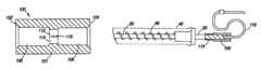
- the thermocouple 46as shown in FIGS. 3-4 , includes a sheath 48 , a support tube 50 , a collar 51 , a first wire 52 , a second wire 54 , a spring 56 , a retainer 58 , and a plug 60 .
- the support tube 50is a substantially cylindrical, elongated member having a longitudinal axis B, as illustrated in FIGS. 6-7 .
- the cross-sectional shape of the support tube 50is square.
- the cross-sectional shape of the support tube 50is oval. It should be understood by one skilled in the art that the cross-sectional shape of the support tube 50 may be formed as any shape.
- the support tube 50may be formed of any type of ceramic or other material sufficient to withstand the cyclic temperature variations as well as the range of temperatures to which the thermocouple 46 is exposed. It should be understood by one skilled in the art that although the illustrated thermocouple 46 is substantially linear, the thermocouple 46 may be formed of any shape sufficient to allow the measuring tip 68 of the thermocouple 46 to be disposed at a desired location.
- the support tube 50 of the thermocouple 46includes a first distal end 62 and an opposing second distal end 64 , as shown in FIG. 6 .
- the support tube 50includes a pair of bores 66 , as shown from the end view in FIG. 7 , extending longitudinally from the first distal end 62 to the second distal end 64 .
- the support tube 50includes more than two bores 66 extending at least a portion of the distance between the first distal end 62 of the support tube 50 and the second distal end 64 . It should be understood by one skilled in the art that the support tube 50 may include any number of bores or holes formed therein either longitudinally or at any other angle relative to the longitudinal axis of the ceramic member.
- One of the bores 66is adapted to receive the first wire 52
- the other of the bores 66is adapted to receive the second wire 54 .
- the bores 66are disposed in a spaced-apart manner to separate the first and second wires 52 , 54 to prevent a short circuit.
- the bores 66are sized to receive the first and second wires 52 , 54 therewithin and provide a small gap between the outer surface of the wires 52 , 54 and the inner surface of the bores 66 .
- the diameter of each bore 66is about 0.016 inches. In another embodiment, the diameter of each bore 66 is about 0.014 inches.
- the bores 66can have any diameter sufficient to receive a first and second wire 52 , 54 while providing a gap between the wires and the surface of the corresponding bore to allow the wires 52 , 54 to expand radially and longitudinally as a result of thermal expansion.
- the support tube 50is at least partially disposed within a protective sheath 48 , as shown in FIGS. 4 and 8 .
- the sheath 48is formed of a transparent quartz material.
- the transparent quartz materialallows substantially all of the radiant energy emitted from the heating elements 16 and the spot lamps 26 to pass therethrough without a noticeable increase in temperature of the sheath 48 .
- the sheath 48has the same general cross-sectional shape as the support tube 50 disposed therewithin, but the sheath 48 is slightly larger to provide a small gap between the inner surface of the sheath 48 and the outer surface of the support tube 50 .
- the sheath 48includes a measuring tip 68 at one end thereof and an opening 70 at the opposing end thereof.
- the sheath 48may be coated with silicon nitride (SiN) or have other surface treatments applied thereto to extend the life of the sheath during chemical vapor deposition (“CVD”) processing in the reaction chamber 12 .
- a cap(not shown), such as a silicon-carbide (SiC) cap, is applied at the measuring tip 68 of the sheath to provide better heat transfer between the ambient environment and the wires 52 , 54 .
- the measuring tip 68is located at the distal end of the sheath 48 .
- the thermocouple 46is employed as a central temperature sensor 36 ( FIG. 1 )
- the measuring tip 68is located immediately adjacent to the lower surface of the substrate holder 28 .
- the measuring tip 68 of the thermocouple 46is configured to measure the temperature of the substrate holder 28 immediately adjacent thereto.
- the first and second wires 52 , 54extend beyond the first distal end 62 of the support tube 50 , as shown in FIG. 5 .
- first and second wires 52 , 54are fused together to form a junction 72 bead, thereby providing an electrical connection between the first and second wires 52 , 54 .
- the first and second wires 52 , 54are melted together to form the junction 72 .
- the first and second wires 52are fused together by soldering. It should be understood by one skilled in the art that the first and second wires 52 , 54 can be fused together in any manner sufficient to provide an electrical connection between the ends of the first and second wires 52 , 54 .
- the free ends of the wires 52 , 54 opposite the junction 72extend from the second distal end 64 of the support tube 50 .
- the wires 52 , 54are formed of dissimilar metals to form a thermocouple therebetween.
- the first wire 52is formed of Platinum
- the second wire 54is formed of a Platinum alloy having 13% Rhodium.
- the wires 52 , 54can be formed of any dissimilar metals sufficient to form a thermocouple therebetween.
- the diameter of the wires 52 , 54are about 0.010 inches. In another embodiment, the diameter of the wires 52 , 54 are about 0.014 inches. It should be understood by one skilled in the art that the wires can be of any diameter sufficient to withstand the cyclical temperature changes during CVD processing as well as withstand the range of temperatures to which the thermocouple 46 is exposed. It should also be understood by one skilled in the art that the diameter of the first and second wires 52 , 54 may not be the same diameter.
- the first and second wires 52 , 54extend from the junction 72 through the spaced-apart bores 66 formed in the support tube 50 and exit the bores 66 at the second distal end 64 of the support tube 50 , as shown in FIG. 10 .
- the second distal end 64 of the support tube 50extends outwardly beyond the opening 70 of the sheath 48 .
- a collar 51is operatively connected to the outer surface of the support tube 50 at a spaced-apart distance from the second distal end 64 of the support tube 50 .
- the collar 51may be formed separately from the support tube 50 and later fixedly attached to the support tube 50 .
- the support tube 50 and the collar 51may be formed as a single member. The collar 51 provides a contact surface against which one end of the spring 56 is maintained.
- a retainer 58is disposed within the opening 70 of the sheath 48 .
- the retainer 58includes a ring 74 , a body 76 , and an aperture 78 extending longitudinally through the ring 74 and body 76 .
- the retainer 58is disposed adjacent to the end of the sheath 48 and is configured to receive the support tube 50 within the aperture 78 .
- the retainer 58is secured within the opening 70 of the sheath 48 by an interference fit, or friction fit. It should be understood by one skilled in the art that the retainer 58 may be secured to the sheath 48 by any other means sufficient to maintain the retainer 58 in a substantially fixed relationship relative to the sheath 48 .
- the retainer 58provides an outlet from the sheath 48 through a reduced diameter, thereby maintaining the support tube 50 in a spaced-apart manner relative to the inner surface of the sheath 48 .
- the support tube 50is disposed within the aperture 78 of the retainer 58 such that the support tube 50 is free to translate within the aperture 78 in a direction substantially parallel to the longitudinal axis B of the support tube 50 .
- a spring 56is located about the outer surface of the support tube 50 between the collar 51 and the retainer 58 .
- the spring 56applies a spring, or biasing, force onto the collar 51 to bias the support tube 50 toward the measuring tip 68 of the sheath 48 .
- the spring 56is configured to maintain the junction 72 formed by the first and second wires 52 , 54 in contact with the measuring tip 68 of the sheath 48 . If the junction 72 were to move away from the measuring tip 68 , the accuracy of the measured temperature would decrease as the junction 72 is spaced a greater distance away from the location being measured. Accordingly, the spring 56 can be configured to bias the junction 72 into contact with the measuring tip 68 , thereby ensuring the junction 72 is touching or located immediately adjacent to the inner surface of the measuring tip 68 .
- the second distal end 64 of the support tube 50extends beyond the sheath 48 through the retainer 58 .
- a cap 100is operatively attached to the second distal end 64 of the support tube 50 in a substantially fixed manner such that the cap 100 is prevented from rotating relative to the support tube 50 .
- the cap 100is formed of Delrin® plastic.
- the cap 100is formed of polyetheretherkeytones (PEEK).
- the cap 100is formed of polyetherimide (PEI).
- PEEK and PEIprovide greater durability. It should be understood by one skilled in the art that the cap 100 may be formed of any material sufficient to withstand large temperature ranges as well as resist torsional movement relative to the sheath 48 .
- the cap 100is an elongated, one-piece cylindrical member having a body 101 , a first end 102 , and a second end 104 .
- the body 101 of the cap 100has a square cross-sectional shape. It should be understood by one skilled in the art that the body 101 of the cap 100 may have any cross-sectional shape.
- a first bore 106is formed into the body 101 .
- the first bore 106extends from the first end 102 along at least a portion of the longitudinal length of the body 101 .
- the first bore 106is circular.
- the first bore 106is configured to receive the second distal end of the support tube 50 .
- the shape of the first bore 106is substantially the same size and shape as the outer surface of the support tube 50 .
- a second bore 108is formed into the second end 104 of the body 101 .
- the second bore 108extends from the second end 104 along at least a portion of the longitudinal length of the cap 100 .
- the cross-sectional shape of the second bore 108may be round, oval, square, or any other shape sufficient to envelop the first and second wires 52 , 54 as the wires exit the support tube 50 .
- the cross-sectional shape of the second bore 108is the same as the first bore 106 .
- the cross-sectional shape of the second bore 108is different than the first bore 106 .
- the first bore 106 and the second bore 108extend from the first and second ends 102 , 104 of the cap 100 , respectively, substantially the same distance, as shown in FIG. 10C .
- the length of the first and second bore 106 , 108may be the same, the first bore 106 may be longer than the second bore 108 , or the second bore may be longer than the first bore 106 .
- the size and shape of the first and second bores 106 , 108are substantially the same such that either bore may receive the second distal end 64 of the support tube 50 , thereby ensuring that the cap 100 is correctly assembled in the thermocouple 46 .
- the size and shape of the first and second bores 106 , 108are different such that the first bore 106 is the only bore capable of receiving the second distal end 64 of the support tube 50 .
- the first and second bores 106 , 108are separated by a web 110 .
- the web 110forms the base of both bores 106 , 108 in the cap 100 .
- the surface of the web 110 at the base of the first bore 106can be substantially the same shape as the end surface of the second distal end 64 of the support tube 50 such that the end surface of the second distal end 64 is disposed in an abutting relationship with the corresponding surface of the web 110 .
- a first aperture 112 and a second aperture 114are formed through the web 110 .
- the first aperture 112is configured to receive the first wire 52 that extends from the second distal end 64 of the support tube 50
- the second aperture 114is configured to receive the second wire 54 that likewise extends from the second distal end 64 of the support tube 50
- the diameter of the first and second apertures 112 , 114are substantially the same diameter as the diameter of the bores 66 of the support tube 50
- the diameter of the first and second apertures 112 , 114are slightly larger than the diameter of the corresponding bores 66 of the support tube 50 .
- the gap between the inner surface of the apertures 112 , 114 and the wires 52 , 54 received thereinallows the wires 52 , 54 to expand or contract radially as well as translate in the longitudinal direction within the apertures 112 , 114 due to thermal expansion or contraction.
- the diameter of the first and second apertures 112 , 114is larger than about 0.010 inches. In another embodiment, the diameter of the first and second apertures 112 , 114 is larger than about 0.014 inches. In yet another embodiment, the diameter of the first and second apertures 112 , 114 is about 0.016 inches.
- the diameters of the apertures 112 , 114should be slightly larger than the diameter of the wire 52 , 54 received therein to allow the wires 52 , 54 to freely radially expand or contract or translate therethrough when the wires 52 , 54 are subject to thermal expansion or contraction.
- the diameter of the first aperture 112is substantially the same as the diameter of the second aperture 114 . In another embodiment, the diameter of the first aperture 112 is different than the diameter of the second aperture 114 .
- the first and second apertures 112 , 114are aligned with the bores 66 of the support tube 50 such that the first and second wires 52 , 54 extend from the second distal end 64 of the support tube 50 and through the web 110 of the cap 100 in a substantially linear manner, as shown in FIG. 10 .
- the portion of the wires 52 , 54 extending from the second distal end 64 of the support tube 50are pulled through the web 110 such that the second distal end 64 of the support tube 50 contacts the corresponding surface of the web 110 , thereby positively locating the support tube 50 within the cap 100 .
- any potential shearing stress resulting from a mis-aligned cap 100 relative to the support tube 50can be greatly reduced or eliminated. Additionally, a properly aligned cap 100 also ensures that the wires 52 , 54 remain spaced apart, thereby avoiding a potential short circuit if the wires 52 , 54 were to contact each other. As the wires 52 , 54 extend through the bores 66 of the support tube 50 and through the apertures 112 , 114 in the web 110 of the cap 100 , the wires remain separated and exposed, without a protective covering. The spaced-apart bores and apertures safely maintain the wires 52 , 54 in a spaced-apart, separated relationship.
- the first and second wires 52 , 54 that extend from the support tube 50 through the apertures 112 , 114 in the cap 100are covered with a Teflon® tube 116 to further prevent the wires from contacting each other and causing a short circuit, as shown in FIG. 10 .
- the second bore 108 formed in the cap 100is sized to receive both the first and second wires 52 , 54 having the Teflon® tube 116 encasing each wire.
- Each of the wires 52 , 54is inserted into a tube 116 such that the end of each tube 116 is located within the second bore 108 of the cap 100 .
- both tubes 116 covering the wires 52 , 54are in an abutting relationship with the web 110 prior to the thermocouple 46 being installed into a tool.
- the end of both tubes 116are slightly spaced-apart from the web 110 to ensure that the first and second wires 52 , 54 are not in tension when assembled.
- the tubes 116cover each of the wires 52 , 54 between the cap 100 and the plug 60 , to which the wires 52 , 54 are attached. In the embodiment illustrated in FIGS.
- the second bore 108is oval shaped so that the opening of the second bore 108 is large enough to receive the pair of tubes 116 surrounding the first and second wires 52 , 54 while preventing the first and second wires 52 , 54 from twisting together as the wires exit the web 110 .
- FIGS. 9-14illustrate an exemplary assembly process for assembling the thermocouple 46 .
- FIGS. 9-10show the support tube 50 inserted into the first bore 106 of the cap 100 in which the first and second apertures 112 , 114 through the web 110 of the cap 100 are aligned with the bores 66 of the support tube 50 such that the wires 52 , 54 remain substantially linearly aligned and in a spaced-apart relationship.
- the wires 52 , 54 extending from the first and second apertures 112 , 114 in the cap 100are covered by the Teflon® tubes 116 .
- FIG. 11shows that the covered wires 52 , 54 form a loop 118 extending from the second bore 108 of the cap 100 .
- the radius of curvature of the loop 118is about 12 mm. In an embodiment, the radius of curvature of the loop 118 is between about 2 mm and about 25 mm. In another embodiment, the radius of curvature of the loop 118 is between about 2 mm and about 12 mm. In a further embodiment, the radius of curvature of the loop 118 is about 5 mm. It should be understood by one skilled in the art that the loop 118 formed by the first and second wires 52 , 54 can have any radius of curvature sufficient to allow the first and second wires 52 , 54 to freely translate longitudinally within the corresponding bores 66 of the support tube 50 without tension or compression stresses being introduced into the wires 52 , 54 .
- a first shrink sleeve 119is disposed about the support tube 50 , as shown in FIGS. 9-11 .
- the first shrink sleeve 119is disposed adjacent to the first end 102 of the cap 100 .
- FIG. 12illustrates an embodiment in which a second shrink sleeve 120 is disposed about the first end 102 of the cap 100 and the first shrink sleeve 119 .
- the first shrink sleeve 119provides an increased diameter about the support tube 50 in the area adjacent to the first end 102 of the cap 100 to provide a more secure connection between the second shrink sleeve 120 and the first shrink sleeve 119 and cap 100 .
- the second shrink sleeve 120is adapted to maintain the alignment between the bores 66 in the support tube 50 with the first and second apertures 112 , 114 in the web 110 of the cap 100 .
- the second shrink sleeve 120is also configured to prevent rotation of the cap 100 relative to the support tube 50 .
- the cap 100includes an indexing detent (not shown) and the support tube 50 includes an indexing protrusion (not shown) adapted to be received in the indexing detent to positively locate the cap 100 relative to the support tube 50 and to prevent rotation of the cap 100 relative to the support tube 50 .
- the second distal end 64 of the support tube 50is flattened and the first bore 106 in the cap has a corresponding cross-sectional area, thereby preventing the cap 100 from rotating relative to the support tube 50 .
- a protective sleeve 122is disposed about the cap 100 and the support tube 50 , as shown in FIG. 13 .
- thermocouple 46is then incorporated into a machine or tool requiring a temperature sensor.
- the measuring tip 68 of the sheath 48is disposed at a position at which a temperature measurement is desired.
- the support tube 50 and the wires 52 , 54expand or contract, particularly along the longitudinal axis B of the support tube 50 .
- the coefficient of thermal expansion of the wires 52 , 54is substantially different than the coefficient of thermal expansion of the support tube 50 , wherein the amount of thermal expansion of the wires 52 , 54 in the longitudinal direction is greater than the thermal expansion of the support tube 50 in the same direction.
- the coefficient of thermal expansion of the wires 52 , 54is similar to the coefficient of thermal expansion of the support tube 50 .
- the coefficient of thermal expansion of the wires 52 , 54is substantially the same as the coefficient of thermal expansion of the support tube 50 .
- the cap 100 attached to the second distal end 64 of the support tube 50translates in the same manner.
- the cap 100does not prevent the support tube 50 from expanding or contracting freely along the longitudinal axis B, thereby eliminating any longitudinal stresses that would otherwise result if the second distal end 64 of the support tube 50 were fixed relative to the sheath 48 .
- the cap 100also maintains the alignment of the wires 52 , 54 exiting the support tube 50 such that the wires 52 , 54 remain in a spaced-apart relationship, thereby preventing a short circuit.
- the wires 52 , 54When the wires 52 , 54 expand or contract in the longitudinal direction a greater magnitude than the support tube 50 , the wires 52 , 54 freely slide, or translate, through the corresponding aperture 112 , 114 of the cap 100 .
- the apertures 112 , 114allow the wires 52 , 54 to freely expand or contract relative to the support tube 50 , thereby reducing or eliminating the tension or compression stresses applied to the wires 52 , 54 that would otherwise be introduced if the free ends of the wires were folded or substantially fixed relative to the support tube 50 .
- the wires 52 , 54are free to translate through the apertures 112 , 114 without significant resistance introduced by the apertures themselves, such as resistance that would result if the apertures 112 , 114 formed a snug fit or interference fit around the wires 52 , 54 .
- the apertures 112 , 114should be sized to provide a small gap between the inner surface of the aperture and the outer surface of the corresponding wire.
- the distance between the apertures 112 , 114 formed through the web 110 of the cap 100be spaced apart a sufficient distance such that when a portion of the wires 52 , 54 is exposed when the wires 52 , 54 thermally expand longitudinally as a result of an increase in temperature of the wires 52 , 54 , the exposed portions of the wires 52 , 54 remain sufficiently spaced apart such that they do not contact each other to cause a short circuit. Further, the loop 118 expands or contracts in a corresponding manner as the wires 52 , 54 expand or contract due to thermal expansion or contraction.
- the radius of curvature of the loop 118should be sufficient to allow the wires 52 , 54 to freely expand or contract without introducing any additional axial loads to the wires 52 , 54 . Allowing the wires 52 , 54 to freely expand or contract in response to the change in temperature of the wires increases the longevity of the thermocouple 46 by reducing or eliminating axial loads that tend to cause grain slip, and eventually premature failure, of the wires 52 , 54 .
- the coefficient of thermal expansion of the support tube 50can be different than the coefficient of thermal expansion of the wires 52 , 54 .
- the support tube 50dissipates energy into the surrounding environment through the outer and end surfaces of the support tube, whereas the energy dissipated from the wires 52 , 54 is transferred to the support tube 50 .
- the support tube 50will expand at a different rate than the first and second wires 52 , 54 due to a temperature difference therebetween.
- the support tube 50will generally be at a different temperature than the wires 52 , 54 received therein due to the differences in the thermal conductivity and specific heat as well as the rate at which energy is dissipated between the support tube 50 and the wires 52 , 54 . Accordingly, the improved thermocouple 42 allows the wires 52 , 54 to thermally expand or contract independent of the support tube 50 such that additional compression or tension stresses are not introduced into the wires 52 , 54 as they expand or contract relative to the support tube 50 .
Landscapes
- Physics & Mathematics (AREA)
- General Physics & Mathematics (AREA)
- Measuring Temperature Or Quantity Of Heat (AREA)
- Chemical Vapour Deposition (AREA)
- Control Of Combustion (AREA)
- Devices For Use In Laboratory Experiments (AREA)
Abstract
Description
Claims (9)
Priority Applications (1)
| Application Number | Priority Date | Filing Date | Title |
|---|---|---|---|
| US12/121,085US7874726B2 (en) | 2007-05-24 | 2008-05-15 | Thermocouple |
Applications Claiming Priority (2)
| Application Number | Priority Date | Filing Date | Title |
|---|---|---|---|
| US94001207P | 2007-05-24 | 2007-05-24 | |
| US12/121,085US7874726B2 (en) | 2007-05-24 | 2008-05-15 | Thermocouple |
Publications (2)
| Publication Number | Publication Date |
|---|---|
| US20080289574A1 US20080289574A1 (en) | 2008-11-27 |
| US7874726B2true US7874726B2 (en) | 2011-01-25 |
Family
ID=39637643
Family Applications (1)
| Application Number | Title | Priority Date | Filing Date |
|---|---|---|---|
| US12/121,085Active2029-02-23US7874726B2 (en) | 2007-05-24 | 2008-05-15 | Thermocouple |
Country Status (8)
| Country | Link |
|---|---|
| US (1) | US7874726B2 (en) |
| EP (1) | EP2156155B1 (en) |
| JP (1) | JP5255054B2 (en) |
| CN (1) | CN101663569B (en) |
| AT (1) | ATE498119T1 (en) |
| DE (1) | DE602008004911D1 (en) |
| TW (1) | TWI439680B (en) |
| WO (1) | WO2008147731A1 (en) |
Cited By (359)
| Publication number | Priority date | Publication date | Assignee | Title |
|---|---|---|---|---|
| US20090110026A1 (en)* | 2007-10-24 | 2009-04-30 | Heraeus Electro-Nite Co. | Expendable immersion device |
| US20100145547A1 (en)* | 2008-12-08 | 2010-06-10 | Asm America, Inc. | Thermocouple |
| US20100284438A1 (en)* | 2009-05-06 | 2010-11-11 | Asm America, Inc. | Thermocouple |
| US20110002358A1 (en)* | 2009-07-02 | 2011-01-06 | Renesas Technology America, Inc. | Temperature Detection and Reporting System and Method in Power Driving and/or Consuming System |
| US8382370B2 (en) | 2009-05-06 | 2013-02-26 | Asm America, Inc. | Thermocouple assembly with guarded thermocouple junction |
| USD702188S1 (en) | 2013-03-08 | 2014-04-08 | Asm Ip Holding B.V. | Thermocouple |
| US9297705B2 (en) | 2009-05-06 | 2016-03-29 | Asm America, Inc. | Smart temperature measuring device |
| US10229833B2 (en) | 2016-11-01 | 2019-03-12 | Asm Ip Holding B.V. | Methods for forming a transition metal nitride film on a substrate by atomic layer deposition and related semiconductor device structures |
| US10249577B2 (en) | 2016-05-17 | 2019-04-02 | Asm Ip Holding B.V. | Method of forming metal interconnection and method of fabricating semiconductor apparatus using the method |
| US10249524B2 (en) | 2017-08-09 | 2019-04-02 | Asm Ip Holding B.V. | Cassette holder assembly for a substrate cassette and holding member for use in such assembly |
| US10262859B2 (en) | 2016-03-24 | 2019-04-16 | Asm Ip Holding B.V. | Process for forming a film on a substrate using multi-port injection assemblies |
| US10269558B2 (en) | 2016-12-22 | 2019-04-23 | Asm Ip Holding B.V. | Method of forming a structure on a substrate |
| US10276355B2 (en) | 2015-03-12 | 2019-04-30 | Asm Ip Holding B.V. | Multi-zone reactor, system including the reactor, and method of using the same |
| US10283353B2 (en) | 2017-03-29 | 2019-05-07 | Asm Ip Holding B.V. | Method of reforming insulating film deposited on substrate with recess pattern |
| US10290508B1 (en) | 2017-12-05 | 2019-05-14 | Asm Ip Holding B.V. | Method for forming vertical spacers for spacer-defined patterning |
| US10312055B2 (en) | 2017-07-26 | 2019-06-04 | Asm Ip Holding B.V. | Method of depositing film by PEALD using negative bias |
| US10312129B2 (en) | 2015-09-29 | 2019-06-04 | Asm Ip Holding B.V. | Variable adjustment for precise matching of multiple chamber cavity housings |
| US10319588B2 (en) | 2017-10-10 | 2019-06-11 | Asm Ip Holding B.V. | Method for depositing a metal chalcogenide on a substrate by cyclical deposition |
| US10322384B2 (en) | 2015-11-09 | 2019-06-18 | Asm Ip Holding B.V. | Counter flow mixer for process chamber |
| US10340125B2 (en) | 2013-03-08 | 2019-07-02 | Asm Ip Holding B.V. | Pulsed remote plasma method and system |
| US10340135B2 (en) | 2016-11-28 | 2019-07-02 | Asm Ip Holding B.V. | Method of topologically restricted plasma-enhanced cyclic deposition of silicon or metal nitride |
| US10343920B2 (en) | 2016-03-18 | 2019-07-09 | Asm Ip Holding B.V. | Aligned carbon nanotubes |
| US10361201B2 (en) | 2013-09-27 | 2019-07-23 | Asm Ip Holding B.V. | Semiconductor structure and device formed using selective epitaxial process |
| US10366864B2 (en) | 2013-03-08 | 2019-07-30 | Asm Ip Holding B.V. | Method and system for in-situ formation of intermediate reactive species |
| US10367080B2 (en) | 2016-05-02 | 2019-07-30 | Asm Ip Holding B.V. | Method of forming a germanium oxynitride film |
| US10364496B2 (en) | 2011-06-27 | 2019-07-30 | Asm Ip Holding B.V. | Dual section module having shared and unshared mass flow controllers |
| US10364493B2 (en) | 2016-08-25 | 2019-07-30 | Asm Ip Holding B.V. | Exhaust apparatus and substrate processing apparatus having an exhaust line with a first ring having at least one hole on a lateral side thereof placed in the exhaust line |
| US10381226B2 (en) | 2016-07-27 | 2019-08-13 | Asm Ip Holding B.V. | Method of processing substrate |
| US10381219B1 (en) | 2018-10-25 | 2019-08-13 | Asm Ip Holding B.V. | Methods for forming a silicon nitride film |
| US10378106B2 (en) | 2008-11-14 | 2019-08-13 | Asm Ip Holding B.V. | Method of forming insulation film by modified PEALD |
| US10388513B1 (en) | 2018-07-03 | 2019-08-20 | Asm Ip Holding B.V. | Method for depositing silicon-free carbon-containing film as gap-fill layer by pulse plasma-assisted deposition |
| US10388509B2 (en) | 2016-06-28 | 2019-08-20 | Asm Ip Holding B.V. | Formation of epitaxial layers via dislocation filtering |
| US10395919B2 (en) | 2016-07-28 | 2019-08-27 | Asm Ip Holding B.V. | Method and apparatus for filling a gap |
| US10403504B2 (en) | 2017-10-05 | 2019-09-03 | Asm Ip Holding B.V. | Method for selectively depositing a metallic film on a substrate |
| US10410943B2 (en) | 2016-10-13 | 2019-09-10 | Asm Ip Holding B.V. | Method for passivating a surface of a semiconductor and related systems |
| US10435790B2 (en) | 2016-11-01 | 2019-10-08 | Asm Ip Holding B.V. | Method of subatmospheric plasma-enhanced ALD using capacitively coupled electrodes with narrow gap |
| US10438965B2 (en) | 2014-12-22 | 2019-10-08 | Asm Ip Holding B.V. | Semiconductor device and manufacturing method thereof |
| US10446393B2 (en) | 2017-05-08 | 2019-10-15 | Asm Ip Holding B.V. | Methods for forming silicon-containing epitaxial layers and related semiconductor device structures |
| US10458018B2 (en) | 2015-06-26 | 2019-10-29 | Asm Ip Holding B.V. | Structures including metal carbide material, devices including the structures, and methods of forming same |
| US10468262B2 (en) | 2017-02-15 | 2019-11-05 | Asm Ip Holding B.V. | Methods for forming a metallic film on a substrate by a cyclical deposition and related semiconductor device structures |
| US10468251B2 (en) | 2016-02-19 | 2019-11-05 | Asm Ip Holding B.V. | Method for forming spacers using silicon nitride film for spacer-defined multiple patterning |
| US10480072B2 (en) | 2009-04-06 | 2019-11-19 | Asm Ip Holding B.V. | Semiconductor processing reactor and components thereof |
| US10483099B1 (en) | 2018-07-26 | 2019-11-19 | Asm Ip Holding B.V. | Method for forming thermally stable organosilicon polymer film |
| US10504742B2 (en) | 2017-05-31 | 2019-12-10 | Asm Ip Holding B.V. | Method of atomic layer etching using hydrogen plasma |
| US10501866B2 (en) | 2016-03-09 | 2019-12-10 | Asm Ip Holding B.V. | Gas distribution apparatus for improved film uniformity in an epitaxial system |
| US10510536B2 (en) | 2018-03-29 | 2019-12-17 | Asm Ip Holding B.V. | Method of depositing a co-doped polysilicon film on a surface of a substrate within a reaction chamber |
| US10529563B2 (en) | 2017-03-29 | 2020-01-07 | Asm Ip Holdings B.V. | Method for forming doped metal oxide films on a substrate by cyclical deposition and related semiconductor device structures |
| US10529554B2 (en) | 2016-02-19 | 2020-01-07 | Asm Ip Holding B.V. | Method for forming silicon nitride film selectively on sidewalls or flat surfaces of trenches |
| US10529542B2 (en) | 2015-03-11 | 2020-01-07 | Asm Ip Holdings B.V. | Cross-flow reactor and method |
| US10535516B2 (en) | 2018-02-01 | 2020-01-14 | Asm Ip Holdings B.V. | Method for depositing a semiconductor structure on a surface of a substrate and related semiconductor structures |
| US10541333B2 (en) | 2017-07-19 | 2020-01-21 | Asm Ip Holding B.V. | Method for depositing a group IV semiconductor and related semiconductor device structures |
| US10541173B2 (en) | 2016-07-08 | 2020-01-21 | Asm Ip Holding B.V. | Selective deposition method to form air gaps |
| US10559458B1 (en) | 2018-11-26 | 2020-02-11 | Asm Ip Holding B.V. | Method of forming oxynitride film |
| US10566223B2 (en) | 2012-08-28 | 2020-02-18 | Asm Ip Holdings B.V. | Systems and methods for dynamic semiconductor process scheduling |
| US10561975B2 (en) | 2014-10-07 | 2020-02-18 | Asm Ip Holdings B.V. | Variable conductance gas distribution apparatus and method |
| US10590535B2 (en) | 2017-07-26 | 2020-03-17 | Asm Ip Holdings B.V. | Chemical treatment, deposition and/or infiltration apparatus and method for using the same |
| US10600673B2 (en) | 2015-07-07 | 2020-03-24 | Asm Ip Holding B.V. | Magnetic susceptor to baseplate seal |
| US10604847B2 (en) | 2014-03-18 | 2020-03-31 | Asm Ip Holding B.V. | Gas distribution system, reactor including the system, and methods of using the same |
| US10605530B2 (en) | 2017-07-26 | 2020-03-31 | Asm Ip Holding B.V. | Assembly of a liner and a flange for a vertical furnace as well as the liner and the vertical furnace |
| US10607895B2 (en) | 2017-09-18 | 2020-03-31 | Asm Ip Holdings B.V. | Method for forming a semiconductor device structure comprising a gate fill metal |
| US10612136B2 (en) | 2018-06-29 | 2020-04-07 | ASM IP Holding, B.V. | Temperature-controlled flange and reactor system including same |
| USD880437S1 (en) | 2018-02-01 | 2020-04-07 | Asm Ip Holding B.V. | Gas supply plate for semiconductor manufacturing apparatus |
| US10612137B2 (en) | 2016-07-08 | 2020-04-07 | Asm Ip Holdings B.V. | Organic reactants for atomic layer deposition |
| US10622375B2 (en) | 2016-11-07 | 2020-04-14 | Asm Ip Holding B.V. | Method of processing a substrate and a device manufactured by using the method |
| US10643904B2 (en) | 2016-11-01 | 2020-05-05 | Asm Ip Holdings B.V. | Methods for forming a semiconductor device and related semiconductor device structures |
| US10643826B2 (en) | 2016-10-26 | 2020-05-05 | Asm Ip Holdings B.V. | Methods for thermally calibrating reaction chambers |
| US10658205B2 (en) | 2017-09-28 | 2020-05-19 | Asm Ip Holdings B.V. | Chemical dispensing apparatus and methods for dispensing a chemical to a reaction chamber |
| US10658181B2 (en) | 2018-02-20 | 2020-05-19 | Asm Ip Holding B.V. | Method of spacer-defined direct patterning in semiconductor fabrication |
| US10655221B2 (en) | 2017-02-09 | 2020-05-19 | Asm Ip Holding B.V. | Method for depositing oxide film by thermal ALD and PEALD |
| US10665452B2 (en) | 2016-05-02 | 2020-05-26 | Asm Ip Holdings B.V. | Source/drain performance through conformal solid state doping |
| US10683571B2 (en) | 2014-02-25 | 2020-06-16 | Asm Ip Holding B.V. | Gas supply manifold and method of supplying gases to chamber using same |
| US10685834B2 (en) | 2017-07-05 | 2020-06-16 | Asm Ip Holdings B.V. | Methods for forming a silicon germanium tin layer and related semiconductor device structures |
| US10692741B2 (en) | 2017-08-08 | 2020-06-23 | Asm Ip Holdings B.V. | Radiation shield |
| US10707106B2 (en) | 2011-06-06 | 2020-07-07 | Asm Ip Holding B.V. | High-throughput semiconductor-processing apparatus equipped with multiple dual-chamber modules |
| US10714335B2 (en) | 2017-04-25 | 2020-07-14 | Asm Ip Holding B.V. | Method of depositing thin film and method of manufacturing semiconductor device |
| US10714315B2 (en) | 2012-10-12 | 2020-07-14 | Asm Ip Holdings B.V. | Semiconductor reaction chamber showerhead |
| US10714385B2 (en) | 2016-07-19 | 2020-07-14 | Asm Ip Holding B.V. | Selective deposition of tungsten |
| US10714350B2 (en) | 2016-11-01 | 2020-07-14 | ASM IP Holdings, B.V. | Methods for forming a transition metal niobium nitride film on a substrate by atomic layer deposition and related semiconductor device structures |
| US10731249B2 (en) | 2018-02-15 | 2020-08-04 | Asm Ip Holding B.V. | Method of forming a transition metal containing film on a substrate by a cyclical deposition process, a method for supplying a transition metal halide compound to a reaction chamber, and related vapor deposition apparatus |
| US10734244B2 (en) | 2017-11-16 | 2020-08-04 | Asm Ip Holding B.V. | Method of processing a substrate and a device manufactured by the same |
| US10734497B2 (en) | 2017-07-18 | 2020-08-04 | Asm Ip Holding B.V. | Methods for forming a semiconductor device structure and related semiconductor device structures |
| US10741385B2 (en) | 2016-07-28 | 2020-08-11 | Asm Ip Holding B.V. | Method and apparatus for filling a gap |
| US10755922B2 (en) | 2018-07-03 | 2020-08-25 | Asm Ip Holding B.V. | Method for depositing silicon-free carbon-containing film as gap-fill layer by pulse plasma-assisted deposition |
| US10767789B2 (en) | 2018-07-16 | 2020-09-08 | Asm Ip Holding B.V. | Diaphragm valves, valve components, and methods for forming valve components |
| US10770336B2 (en) | 2017-08-08 | 2020-09-08 | Asm Ip Holding B.V. | Substrate lift mechanism and reactor including same |
| US10770286B2 (en) | 2017-05-08 | 2020-09-08 | Asm Ip Holdings B.V. | Methods for selectively forming a silicon nitride film on a substrate and related semiconductor device structures |
| US10787741B2 (en) | 2014-08-21 | 2020-09-29 | Asm Ip Holding B.V. | Method and system for in situ formation of gas-phase compounds |
| US10797133B2 (en) | 2018-06-21 | 2020-10-06 | Asm Ip Holding B.V. | Method for depositing a phosphorus doped silicon arsenide film and related semiconductor device structures |
| US10804098B2 (en) | 2009-08-14 | 2020-10-13 | Asm Ip Holding B.V. | Systems and methods for thin-film deposition of metal oxides using excited nitrogen-oxygen species |
| US10811256B2 (en) | 2018-10-16 | 2020-10-20 | Asm Ip Holding B.V. | Method for etching a carbon-containing feature |
| US10818758B2 (en) | 2018-11-16 | 2020-10-27 | Asm Ip Holding B.V. | Methods for forming a metal silicate film on a substrate in a reaction chamber and related semiconductor device structures |
| USD900036S1 (en) | 2017-08-24 | 2020-10-27 | Asm Ip Holding B.V. | Heater electrical connector and adapter |
| US10829852B2 (en) | 2018-08-16 | 2020-11-10 | Asm Ip Holding B.V. | Gas distribution device for a wafer processing apparatus |
| US10832903B2 (en) | 2011-10-28 | 2020-11-10 | Asm Ip Holding B.V. | Process feed management for semiconductor substrate processing |
| US10847371B2 (en) | 2018-03-27 | 2020-11-24 | Asm Ip Holding B.V. | Method of forming an electrode on a substrate and a semiconductor device structure including an electrode |
| US10847366B2 (en) | 2018-11-16 | 2020-11-24 | Asm Ip Holding B.V. | Methods for depositing a transition metal chalcogenide film on a substrate by a cyclical deposition process |
| US10847365B2 (en) | 2018-10-11 | 2020-11-24 | Asm Ip Holding B.V. | Method of forming conformal silicon carbide film by cyclic CVD |
| US10844484B2 (en) | 2017-09-22 | 2020-11-24 | Asm Ip Holding B.V. | Apparatus for dispensing a vapor phase reactant to a reaction chamber and related methods |
| US10854498B2 (en) | 2011-07-15 | 2020-12-01 | Asm Ip Holding B.V. | Wafer-supporting device and method for producing same |
| US10851456B2 (en) | 2016-04-21 | 2020-12-01 | Asm Ip Holding B.V. | Deposition of metal borides |
| USD903477S1 (en) | 2018-01-24 | 2020-12-01 | Asm Ip Holdings B.V. | Metal clamp |
| US10858737B2 (en) | 2014-07-28 | 2020-12-08 | Asm Ip Holding B.V. | Showerhead assembly and components thereof |
| US10867786B2 (en) | 2018-03-30 | 2020-12-15 | Asm Ip Holding B.V. | Substrate processing method |
| US10867788B2 (en) | 2016-12-28 | 2020-12-15 | Asm Ip Holding B.V. | Method of forming a structure on a substrate |
| US10865475B2 (en) | 2016-04-21 | 2020-12-15 | Asm Ip Holding B.V. | Deposition of metal borides and silicides |
| US10872771B2 (en) | 2018-01-16 | 2020-12-22 | Asm Ip Holding B. V. | Method for depositing a material film on a substrate within a reaction chamber by a cyclical deposition process and related device structures |
| US10886123B2 (en) | 2017-06-02 | 2021-01-05 | Asm Ip Holding B.V. | Methods for forming low temperature semiconductor layers and related semiconductor device structures |
| US10883175B2 (en) | 2018-08-09 | 2021-01-05 | Asm Ip Holding B.V. | Vertical furnace for processing substrates and a liner for use therein |
| US10892156B2 (en) | 2017-05-08 | 2021-01-12 | Asm Ip Holding B.V. | Methods for forming a silicon nitride film on a substrate and related semiconductor device structures |
| US10896820B2 (en) | 2018-02-14 | 2021-01-19 | Asm Ip Holding B.V. | Method for depositing a ruthenium-containing film on a substrate by a cyclical deposition process |
| US10910262B2 (en) | 2017-11-16 | 2021-02-02 | Asm Ip Holding B.V. | Method of selectively depositing a capping layer structure on a semiconductor device structure |
| US10914004B2 (en) | 2018-06-29 | 2021-02-09 | Asm Ip Holding B.V. | Thin-film deposition method and manufacturing method of semiconductor device |
| US10923344B2 (en) | 2017-10-30 | 2021-02-16 | Asm Ip Holding B.V. | Methods for forming a semiconductor structure and related semiconductor structures |
| US10928731B2 (en) | 2017-09-21 | 2021-02-23 | Asm Ip Holding B.V. | Method of sequential infiltration synthesis treatment of infiltrateable material and structures and devices formed using same |
| US10934619B2 (en) | 2016-11-15 | 2021-03-02 | Asm Ip Holding B.V. | Gas supply unit and substrate processing apparatus including the gas supply unit |
| US10941490B2 (en) | 2014-10-07 | 2021-03-09 | Asm Ip Holding B.V. | Multiple temperature range susceptor, assembly, reactor and system including the susceptor, and methods of using the same |
| US10975470B2 (en) | 2018-02-23 | 2021-04-13 | Asm Ip Holding B.V. | Apparatus for detecting or monitoring for a chemical precursor in a high temperature environment |
| US11001925B2 (en) | 2016-12-19 | 2021-05-11 | Asm Ip Holding B.V. | Substrate processing apparatus |
| US11018002B2 (en) | 2017-07-19 | 2021-05-25 | Asm Ip Holding B.V. | Method for selectively depositing a Group IV semiconductor and related semiconductor device structures |
| US11015245B2 (en) | 2014-03-19 | 2021-05-25 | Asm Ip Holding B.V. | Gas-phase reactor and system having exhaust plenum and components thereof |
| US11018047B2 (en) | 2018-01-25 | 2021-05-25 | Asm Ip Holding B.V. | Hybrid lift pin |
| US11024523B2 (en) | 2018-09-11 | 2021-06-01 | Asm Ip Holding B.V. | Substrate processing apparatus and method |
| US11022879B2 (en) | 2017-11-24 | 2021-06-01 | Asm Ip Holding B.V. | Method of forming an enhanced unexposed photoresist layer |
| US11031242B2 (en) | 2018-11-07 | 2021-06-08 | Asm Ip Holding B.V. | Methods for depositing a boron doped silicon germanium film |
| USD922229S1 (en) | 2019-06-05 | 2021-06-15 | Asm Ip Holding B.V. | Device for controlling a temperature of a gas supply unit |
| US11049751B2 (en) | 2018-09-14 | 2021-06-29 | Asm Ip Holding B.V. | Cassette supply system to store and handle cassettes and processing apparatus equipped therewith |
| US11053591B2 (en) | 2018-08-06 | 2021-07-06 | Asm Ip Holding B.V. | Multi-port gas injection system and reactor system including same |
| US11056567B2 (en) | 2018-05-11 | 2021-07-06 | Asm Ip Holding B.V. | Method of forming a doped metal carbide film on a substrate and related semiconductor device structures |
| US11056344B2 (en) | 2017-08-30 | 2021-07-06 | Asm Ip Holding B.V. | Layer forming method |
| US11069510B2 (en) | 2017-08-30 | 2021-07-20 | Asm Ip Holding B.V. | Substrate processing apparatus |
| US11081345B2 (en) | 2018-02-06 | 2021-08-03 | Asm Ip Holding B.V. | Method of post-deposition treatment for silicon oxide film |
| US11087997B2 (en) | 2018-10-31 | 2021-08-10 | Asm Ip Holding B.V. | Substrate processing apparatus for processing substrates |
| US11088002B2 (en) | 2018-03-29 | 2021-08-10 | Asm Ip Holding B.V. | Substrate rack and a substrate processing system and method |
| US11114294B2 (en) | 2019-03-08 | 2021-09-07 | Asm Ip Holding B.V. | Structure including SiOC layer and method of forming same |
| US11114283B2 (en) | 2018-03-16 | 2021-09-07 | Asm Ip Holding B.V. | Reactor, system including the reactor, and methods of manufacturing and using same |
| USD930782S1 (en) | 2019-08-22 | 2021-09-14 | Asm Ip Holding B.V. | Gas distributor |
| US11127589B2 (en) | 2019-02-01 | 2021-09-21 | Asm Ip Holding B.V. | Method of topology-selective film formation of silicon oxide |
| US11127617B2 (en) | 2017-11-27 | 2021-09-21 | Asm Ip Holding B.V. | Storage device for storing wafer cassettes for use with a batch furnace |
| USD931978S1 (en) | 2019-06-27 | 2021-09-28 | Asm Ip Holding B.V. | Showerhead vacuum transport |
| US11139191B2 (en) | 2017-08-09 | 2021-10-05 | Asm Ip Holding B.V. | Storage apparatus for storing cassettes for substrates and processing apparatus equipped therewith |
| US11139308B2 (en) | 2015-12-29 | 2021-10-05 | Asm Ip Holding B.V. | Atomic layer deposition of III-V compounds to form V-NAND devices |
| US11158513B2 (en) | 2018-12-13 | 2021-10-26 | Asm Ip Holding B.V. | Methods for forming a rhenium-containing film on a substrate by a cyclical deposition process and related semiconductor device structures |
| USD935572S1 (en) | 2019-05-24 | 2021-11-09 | Asm Ip Holding B.V. | Gas channel plate |
| US11171025B2 (en) | 2019-01-22 | 2021-11-09 | Asm Ip Holding B.V. | Substrate processing device |
| US11205585B2 (en) | 2016-07-28 | 2021-12-21 | Asm Ip Holding B.V. | Substrate processing apparatus and method of operating the same |
| US11217444B2 (en) | 2018-11-30 | 2022-01-04 | Asm Ip Holding B.V. | Method for forming an ultraviolet radiation responsive metal oxide-containing film |
| US11222772B2 (en) | 2016-12-14 | 2022-01-11 | Asm Ip Holding B.V. | Substrate processing apparatus |
| USD940837S1 (en) | 2019-08-22 | 2022-01-11 | Asm Ip Holding B.V. | Electrode |
| US11227782B2 (en) | 2019-07-31 | 2022-01-18 | Asm Ip Holding B.V. | Vertical batch furnace assembly |
| US11227789B2 (en) | 2019-02-20 | 2022-01-18 | Asm Ip Holding B.V. | Method and apparatus for filling a recess formed within a substrate surface |
| US11233133B2 (en) | 2015-10-21 | 2022-01-25 | Asm Ip Holding B.V. | NbMC layers |
| US11230766B2 (en) | 2018-03-29 | 2022-01-25 | Asm Ip Holding B.V. | Substrate processing apparatus and method |
| US11232963B2 (en) | 2018-10-03 | 2022-01-25 | Asm Ip Holding B.V. | Substrate processing apparatus and method |
| US11251068B2 (en) | 2018-10-19 | 2022-02-15 | Asm Ip Holding B.V. | Substrate processing apparatus and substrate processing method |
| US11251040B2 (en) | 2019-02-20 | 2022-02-15 | Asm Ip Holding B.V. | Cyclical deposition method including treatment step and apparatus for same |
| USD944946S1 (en) | 2019-06-14 | 2022-03-01 | Asm Ip Holding B.V. | Shower plate |
| US11270899B2 (en) | 2018-06-04 | 2022-03-08 | Asm Ip Holding B.V. | Wafer handling chamber with moisture reduction |
| US11274369B2 (en) | 2018-09-11 | 2022-03-15 | Asm Ip Holding B.V. | Thin film deposition method |
| US11282698B2 (en) | 2019-07-19 | 2022-03-22 | Asm Ip Holding B.V. | Method of forming topology-controlled amorphous carbon polymer film |
| US11289326B2 (en) | 2019-05-07 | 2022-03-29 | Asm Ip Holding B.V. | Method for reforming amorphous carbon polymer film |
| US11286562B2 (en) | 2018-06-08 | 2022-03-29 | Asm Ip Holding B.V. | Gas-phase chemical reactor and method of using same |
| US11286558B2 (en) | 2019-08-23 | 2022-03-29 | Asm Ip Holding B.V. | Methods for depositing a molybdenum nitride film on a surface of a substrate by a cyclical deposition process and related semiconductor device structures including a molybdenum nitride film |
| USD947913S1 (en) | 2019-05-17 | 2022-04-05 | Asm Ip Holding B.V. | Susceptor shaft |
| US11295980B2 (en) | 2017-08-30 | 2022-04-05 | Asm Ip Holding B.V. | Methods for depositing a molybdenum metal film over a dielectric surface of a substrate by a cyclical deposition process and related semiconductor device structures |
| USD948463S1 (en) | 2018-10-24 | 2022-04-12 | Asm Ip Holding B.V. | Susceptor for semiconductor substrate supporting apparatus |
| USD949319S1 (en) | 2019-08-22 | 2022-04-19 | Asm Ip Holding B.V. | Exhaust duct |
| US11306395B2 (en) | 2017-06-28 | 2022-04-19 | Asm Ip Holding B.V. | Methods for depositing a transition metal nitride film on a substrate by atomic layer deposition and related deposition apparatus |
| US11315794B2 (en) | 2019-10-21 | 2022-04-26 | Asm Ip Holding B.V. | Apparatus and methods for selectively etching films |
| US20220139737A1 (en)* | 2020-10-29 | 2022-05-05 | Kokusai Electric Corporation | Temperature sensor, heater unit, and substrate processing apparatus |
| US11342216B2 (en) | 2019-02-20 | 2022-05-24 | Asm Ip Holding B.V. | Cyclical deposition method and apparatus for filling a recess formed within a substrate surface |
| US11339476B2 (en) | 2019-10-08 | 2022-05-24 | Asm Ip Holding B.V. | Substrate processing device having connection plates, substrate processing method |
| US11345999B2 (en) | 2019-06-06 | 2022-05-31 | Asm Ip Holding B.V. | Method of using a gas-phase reactor system including analyzing exhausted gas |
| US11355338B2 (en) | 2019-05-10 | 2022-06-07 | Asm Ip Holding B.V. | Method of depositing material onto a surface and structure formed according to the method |
| US11361990B2 (en) | 2018-05-28 | 2022-06-14 | Asm Ip Holding B.V. | Substrate processing method and device manufactured by using the same |
| US11374112B2 (en) | 2017-07-19 | 2022-06-28 | Asm Ip Holding B.V. | Method for depositing a group IV semiconductor and related semiconductor device structures |
| US11378337B2 (en) | 2019-03-28 | 2022-07-05 | Asm Ip Holding B.V. | Door opener and substrate processing apparatus provided therewith |
| US11393690B2 (en) | 2018-01-19 | 2022-07-19 | Asm Ip Holding B.V. | Deposition method |
| US11390945B2 (en) | 2019-07-03 | 2022-07-19 | Asm Ip Holding B.V. | Temperature control assembly for substrate processing apparatus and method of using same |
| US11390946B2 (en) | 2019-01-17 | 2022-07-19 | Asm Ip Holding B.V. | Methods of forming a transition metal containing film on a substrate by a cyclical deposition process |
| US11401605B2 (en) | 2019-11-26 | 2022-08-02 | Asm Ip Holding B.V. | Substrate processing apparatus |
| US11414760B2 (en) | 2018-10-08 | 2022-08-16 | Asm Ip Holding B.V. | Substrate support unit, thin film deposition apparatus including the same, and substrate processing apparatus including the same |
| US11424119B2 (en) | 2019-03-08 | 2022-08-23 | Asm Ip Holding B.V. | Method for selective deposition of silicon nitride layer and structure including selectively-deposited silicon nitride layer |
| US11430640B2 (en) | 2019-07-30 | 2022-08-30 | Asm Ip Holding B.V. | Substrate processing apparatus |
| US11430674B2 (en) | 2018-08-22 | 2022-08-30 | Asm Ip Holding B.V. | Sensor array, apparatus for dispensing a vapor phase reactant to a reaction chamber and related methods |
| US11437241B2 (en) | 2020-04-08 | 2022-09-06 | Asm Ip Holding B.V. | Apparatus and methods for selectively etching silicon oxide films |
| US11443926B2 (en) | 2019-07-30 | 2022-09-13 | Asm Ip Holding B.V. | Substrate processing apparatus |
| US11447861B2 (en) | 2016-12-15 | 2022-09-20 | Asm Ip Holding B.V. | Sequential infiltration synthesis apparatus and a method of forming a patterned structure |
| US11447864B2 (en) | 2019-04-19 | 2022-09-20 | Asm Ip Holding B.V. | Layer forming method and apparatus |
| US11453943B2 (en) | 2016-05-25 | 2022-09-27 | Asm Ip Holding B.V. | Method for forming carbon-containing silicon/metal oxide or nitride film by ALD using silicon precursor and hydrocarbon precursor |
| USD965044S1 (en) | 2019-08-19 | 2022-09-27 | Asm Ip Holding B.V. | Susceptor shaft |
| USD965524S1 (en) | 2019-08-19 | 2022-10-04 | Asm Ip Holding B.V. | Susceptor support |
| US11469098B2 (en) | 2018-05-08 | 2022-10-11 | Asm Ip Holding B.V. | Methods for depositing an oxide film on a substrate by a cyclical deposition process and related device structures |
| US11473195B2 (en) | 2018-03-01 | 2022-10-18 | Asm Ip Holding B.V. | Semiconductor processing apparatus and a method for processing a substrate |
| US11476109B2 (en) | 2019-06-11 | 2022-10-18 | Asm Ip Holding B.V. | Method of forming an electronic structure using reforming gas, system for performing the method, and structure formed using the method |
| US11482533B2 (en) | 2019-02-20 | 2022-10-25 | Asm Ip Holding B.V. | Apparatus and methods for plug fill deposition in 3-D NAND applications |
| US11482412B2 (en) | 2018-01-19 | 2022-10-25 | Asm Ip Holding B.V. | Method for depositing a gap-fill layer by plasma-assisted deposition |
| US11482418B2 (en) | 2018-02-20 | 2022-10-25 | Asm Ip Holding B.V. | Substrate processing method and apparatus |
| US11488819B2 (en) | 2018-12-04 | 2022-11-01 | Asm Ip Holding B.V. | Method of cleaning substrate processing apparatus |
| US11488854B2 (en) | 2020-03-11 | 2022-11-01 | Asm Ip Holding B.V. | Substrate handling device with adjustable joints |
| US11492703B2 (en) | 2018-06-27 | 2022-11-08 | Asm Ip Holding B.V. | Cyclic deposition methods for forming metal-containing material and films and structures including the metal-containing material |
| US11495459B2 (en) | 2019-09-04 | 2022-11-08 | Asm Ip Holding B.V. | Methods for selective deposition using a sacrificial capping layer |
| US11499226B2 (en) | 2018-11-02 | 2022-11-15 | Asm Ip Holding B.V. | Substrate supporting unit and a substrate processing device including the same |
| US11499222B2 (en) | 2018-06-27 | 2022-11-15 | Asm Ip Holding B.V. | Cyclic deposition methods for forming metal-containing material and films and structures including the metal-containing material |
| US11501968B2 (en) | 2019-11-15 | 2022-11-15 | Asm Ip Holding B.V. | Method for providing a semiconductor device with silicon filled gaps |
| US11515188B2 (en) | 2019-05-16 | 2022-11-29 | Asm Ip Holding B.V. | Wafer boat handling device, vertical batch furnace and method |
| US11515187B2 (en) | 2020-05-01 | 2022-11-29 | Asm Ip Holding B.V. | Fast FOUP swapping with a FOUP handler |
| US11521851B2 (en) | 2020-02-03 | 2022-12-06 | Asm Ip Holding B.V. | Method of forming structures including a vanadium or indium layer |
| US11527400B2 (en) | 2019-08-23 | 2022-12-13 | Asm Ip Holding B.V. | Method for depositing silicon oxide film having improved quality by peald using bis(diethylamino)silane |
| US11527403B2 (en) | 2019-12-19 | 2022-12-13 | Asm Ip Holding B.V. | Methods for filling a gap feature on a substrate surface and related semiconductor structures |
| US11530483B2 (en) | 2018-06-21 | 2022-12-20 | Asm Ip Holding B.V. | Substrate processing system |
| US11532757B2 (en) | 2016-10-27 | 2022-12-20 | Asm Ip Holding B.V. | Deposition of charge trapping layers |
| US11530876B2 (en) | 2020-04-24 | 2022-12-20 | Asm Ip Holding B.V. | Vertical batch furnace assembly comprising a cooling gas supply |
| US11551912B2 (en) | 2020-01-20 | 2023-01-10 | Asm Ip Holding B.V. | Method of forming thin film and method of modifying surface of thin film |
| US11551925B2 (en) | 2019-04-01 | 2023-01-10 | Asm Ip Holding B.V. | Method for manufacturing a semiconductor device |
| US11557474B2 (en) | 2019-07-29 | 2023-01-17 | Asm Ip Holding B.V. | Methods for selective deposition utilizing n-type dopants and/or alternative dopants to achieve high dopant incorporation |
| USD975665S1 (en) | 2019-05-17 | 2023-01-17 | Asm Ip Holding B.V. | Susceptor shaft |
| US11562901B2 (en) | 2019-09-25 | 2023-01-24 | Asm Ip Holding B.V. | Substrate processing method |
| US11572620B2 (en) | 2018-11-06 | 2023-02-07 | Asm Ip Holding B.V. | Methods for selectively depositing an amorphous silicon film on a substrate |
| US11581186B2 (en) | 2016-12-15 | 2023-02-14 | Asm Ip Holding B.V. | Sequential infiltration synthesis apparatus |
| US11587814B2 (en) | 2019-07-31 | 2023-02-21 | Asm Ip Holding B.V. | Vertical batch furnace assembly |
| US11587815B2 (en) | 2019-07-31 | 2023-02-21 | Asm Ip Holding B.V. | Vertical batch furnace assembly |
| US11594450B2 (en) | 2019-08-22 | 2023-02-28 | Asm Ip Holding B.V. | Method for forming a structure with a hole |
| USD979506S1 (en) | 2019-08-22 | 2023-02-28 | Asm Ip Holding B.V. | Insulator |
| US11594600B2 (en) | 2019-11-05 | 2023-02-28 | Asm Ip Holding B.V. | Structures with doped semiconductor layers and methods and systems for forming same |
| USD980814S1 (en) | 2021-05-11 | 2023-03-14 | Asm Ip Holding B.V. | Gas distributor for substrate processing apparatus |
| USD980813S1 (en) | 2021-05-11 | 2023-03-14 | Asm Ip Holding B.V. | Gas flow control plate for substrate processing apparatus |
| US11605528B2 (en) | 2019-07-09 | 2023-03-14 | Asm Ip Holding B.V. | Plasma device using coaxial waveguide, and substrate treatment method |
| US11610775B2 (en) | 2016-07-28 | 2023-03-21 | Asm Ip Holding B.V. | Method and apparatus for filling a gap |
| US11610774B2 (en) | 2019-10-02 | 2023-03-21 | Asm Ip Holding B.V. | Methods for forming a topographically selective silicon oxide film by a cyclical plasma-enhanced deposition process |
| USD981973S1 (en) | 2021-05-11 | 2023-03-28 | Asm Ip Holding B.V. | Reactor wall for substrate processing apparatus |
| US11615970B2 (en) | 2019-07-17 | 2023-03-28 | Asm Ip Holding B.V. | Radical assist ignition plasma system and method |
| US11626308B2 (en) | 2020-05-13 | 2023-04-11 | Asm Ip Holding B.V. | Laser alignment fixture for a reactor system |
| US11626316B2 (en) | 2019-11-20 | 2023-04-11 | Asm Ip Holding B.V. | Method of depositing carbon-containing material on a surface of a substrate, structure formed using the method, and system for forming the structure |
| US11629406B2 (en) | 2018-03-09 | 2023-04-18 | Asm Ip Holding B.V. | Semiconductor processing apparatus comprising one or more pyrometers for measuring a temperature of a substrate during transfer of the substrate |
| US11629407B2 (en) | 2019-02-22 | 2023-04-18 | Asm Ip Holding B.V. | Substrate processing apparatus and method for processing substrates |
| US11637014B2 (en) | 2019-10-17 | 2023-04-25 | Asm Ip Holding B.V. | Methods for selective deposition of doped semiconductor material |
| US11637011B2 (en) | 2019-10-16 | 2023-04-25 | Asm Ip Holding B.V. | Method of topology-selective film formation of silicon oxide |
| US11639811B2 (en) | 2017-11-27 | 2023-05-02 | Asm Ip Holding B.V. | Apparatus including a clean mini environment |
| US11639548B2 (en) | 2019-08-21 | 2023-05-02 | Asm Ip Holding B.V. | Film-forming material mixed-gas forming device and film forming device |
| US11646204B2 (en) | 2020-06-24 | 2023-05-09 | Asm Ip Holding B.V. | Method for forming a layer provided with silicon |
| US11646205B2 (en) | 2019-10-29 | 2023-05-09 | Asm Ip Holding B.V. | Methods of selectively forming n-type doped material on a surface, systems for selectively forming n-type doped material, and structures formed using same |
| US11643724B2 (en) | 2019-07-18 | 2023-05-09 | Asm Ip Holding B.V. | Method of forming structures using a neutral beam |
| US11646184B2 (en) | 2019-11-29 | 2023-05-09 | Asm Ip Holding B.V. | Substrate processing apparatus |
| US11644758B2 (en) | 2020-07-17 | 2023-05-09 | Asm Ip Holding B.V. | Structures and methods for use in photolithography |
| US11658029B2 (en) | 2018-12-14 | 2023-05-23 | Asm Ip Holding B.V. | Method of forming a device structure using selective deposition of gallium nitride and system for same |
| US11658035B2 (en) | 2020-06-30 | 2023-05-23 | Asm Ip Holding B.V. | Substrate processing method |
| US11664267B2 (en) | 2019-07-10 | 2023-05-30 | Asm Ip Holding B.V. | Substrate support assembly and substrate processing device including the same |
| US11664245B2 (en) | 2019-07-16 | 2023-05-30 | Asm Ip Holding B.V. | Substrate processing device |
| US11664199B2 (en) | 2018-10-19 | 2023-05-30 | Asm Ip Holding B.V. | Substrate processing apparatus and substrate processing method |
| US11674220B2 (en) | 2020-07-20 | 2023-06-13 | Asm Ip Holding B.V. | Method for depositing molybdenum layers using an underlayer |
| US11680839B2 (en) | 2019-08-05 | 2023-06-20 | Asm Ip Holding B.V. | Liquid level sensor for a chemical source vessel |
| USD990441S1 (en) | 2021-09-07 | 2023-06-27 | Asm Ip Holding B.V. | Gas flow control plate |
| US11688603B2 (en) | 2019-07-17 | 2023-06-27 | Asm Ip Holding B.V. | Methods of forming silicon germanium structures |
| US11685991B2 (en) | 2018-02-14 | 2023-06-27 | Asm Ip Holding B.V. | Method for depositing a ruthenium-containing film on a substrate by a cyclical deposition process |
| USD990534S1 (en) | 2020-09-11 | 2023-06-27 | Asm Ip Holding B.V. | Weighted lift pin |
| US11705333B2 (en) | 2020-05-21 | 2023-07-18 | Asm Ip Holding B.V. | Structures including multiple carbon layers and methods of forming and using same |
| US11718913B2 (en) | 2018-06-04 | 2023-08-08 | Asm Ip Holding B.V. | Gas distribution system and reactor system including same |
| US11725277B2 (en) | 2011-07-20 | 2023-08-15 | Asm Ip Holding B.V. | Pressure transmitter for a semiconductor processing environment |
| US11725280B2 (en) | 2020-08-26 | 2023-08-15 | Asm Ip Holding B.V. | Method for forming metal silicon oxide and metal silicon oxynitride layers |
| US11735422B2 (en) | 2019-10-10 | 2023-08-22 | Asm Ip Holding B.V. | Method of forming a photoresist underlayer and structure including same |
| US11742198B2 (en) | 2019-03-08 | 2023-08-29 | Asm Ip Holding B.V. | Structure including SiOCN layer and method of forming same |
| US11769682B2 (en) | 2017-08-09 | 2023-09-26 | Asm Ip Holding B.V. | Storage apparatus for storing cassettes for substrates and processing apparatus equipped therewith |
| US11767589B2 (en) | 2020-05-29 | 2023-09-26 | Asm Ip Holding B.V. | Substrate processing device |
| US11776846B2 (en) | 2020-02-07 | 2023-10-03 | Asm Ip Holding B.V. | Methods for depositing gap filling fluids and related systems and devices |
| US11781221B2 (en) | 2019-05-07 | 2023-10-10 | Asm Ip Holding B.V. | Chemical source vessel with dip tube |
| US11781243B2 (en) | 2020-02-17 | 2023-10-10 | Asm Ip Holding B.V. | Method for depositing low temperature phosphorous-doped silicon |
| US11804364B2 (en) | 2020-05-19 | 2023-10-31 | Asm Ip Holding B.V. | Substrate processing apparatus |
| US11814747B2 (en) | 2019-04-24 | 2023-11-14 | Asm Ip Holding B.V. | Gas-phase reactor system-with a reaction chamber, a solid precursor source vessel, a gas distribution system, and a flange assembly |
| US11823876B2 (en) | 2019-09-05 | 2023-11-21 | Asm Ip Holding B.V. | Substrate processing apparatus |
| US11823866B2 (en) | 2020-04-02 | 2023-11-21 | Asm Ip Holding B.V. | Thin film forming method |
| US11821078B2 (en) | 2020-04-15 | 2023-11-21 | Asm Ip Holding B.V. | Method for forming precoat film and method for forming silicon-containing film |
| US11827981B2 (en) | 2020-10-14 | 2023-11-28 | Asm Ip Holding B.V. | Method of depositing material on stepped structure |
| US11828707B2 (en) | 2020-02-04 | 2023-11-28 | Asm Ip Holding B.V. | Method and apparatus for transmittance measurements of large articles |
| US11830738B2 (en) | 2020-04-03 | 2023-11-28 | Asm Ip Holding B.V. | Method for forming barrier layer and method for manufacturing semiconductor device |
| US11830730B2 (en) | 2017-08-29 | 2023-11-28 | Asm Ip Holding B.V. | Layer forming method and apparatus |
| US11840761B2 (en) | 2019-12-04 | 2023-12-12 | Asm Ip Holding B.V. | Substrate processing apparatus |
| US11876356B2 (en) | 2020-03-11 | 2024-01-16 | Asm Ip Holding B.V. | Lockout tagout assembly and system and method of using same |
| US11873557B2 (en) | 2020-10-22 | 2024-01-16 | Asm Ip Holding B.V. | Method of depositing vanadium metal |
| USD1012873S1 (en) | 2020-09-24 | 2024-01-30 | Asm Ip Holding B.V. | Electrode for semiconductor processing apparatus |
| US11887857B2 (en) | 2020-04-24 | 2024-01-30 | Asm Ip Holding B.V. | Methods and systems for depositing a layer comprising vanadium, nitrogen, and a further element |
| US11885020B2 (en) | 2020-12-22 | 2024-01-30 | Asm Ip Holding B.V. | Transition metal deposition method |
| US11885023B2 (en) | 2018-10-01 | 2024-01-30 | Asm Ip Holding B.V. | Substrate retaining apparatus, system including the apparatus, and method of using same |
| US11885013B2 (en) | 2019-12-17 | 2024-01-30 | Asm Ip Holding B.V. | Method of forming vanadium nitride layer and structure including the vanadium nitride layer |
| US11891696B2 (en) | 2020-11-30 | 2024-02-06 | Asm Ip Holding B.V. | Injector configured for arrangement within a reaction chamber of a substrate processing apparatus |
| US11901179B2 (en) | 2020-10-28 | 2024-02-13 | Asm Ip Holding B.V. | Method and device for depositing silicon onto substrates |
| US11898243B2 (en) | 2020-04-24 | 2024-02-13 | Asm Ip Holding B.V. | Method of forming vanadium nitride-containing layer |
| US11915929B2 (en) | 2019-11-26 | 2024-02-27 | Asm Ip Holding B.V. | Methods for selectively forming a target film on a substrate comprising a first dielectric surface and a second metallic surface |
| US11923181B2 (en) | 2019-11-29 | 2024-03-05 | Asm Ip Holding B.V. | Substrate processing apparatus for minimizing the effect of a filling gas during substrate processing |
| US11929251B2 (en) | 2019-12-02 | 2024-03-12 | Asm Ip Holding B.V. | Substrate processing apparatus having electrostatic chuck and substrate processing method |
| US11946137B2 (en) | 2020-12-16 | 2024-04-02 | Asm Ip Holding B.V. | Runout and wobble measurement fixtures |
| US11959168B2 (en) | 2020-04-29 | 2024-04-16 | Asm Ip Holding B.V. | Solid source precursor vessel |
| US11961741B2 (en) | 2020-03-12 | 2024-04-16 | Asm Ip Holding B.V. | Method for fabricating layer structure having target topological profile |
| USD1023959S1 (en) | 2021-05-11 | 2024-04-23 | Asm Ip Holding B.V. | Electrode for substrate processing apparatus |
| US11967488B2 (en) | 2013-02-01 | 2024-04-23 | Asm Ip Holding B.V. | Method for treatment of deposition reactor |
| US11976359B2 (en) | 2020-01-06 | 2024-05-07 | Asm Ip Holding B.V. | Gas supply assembly, components thereof, and reactor system including same |
| US11987881B2 (en) | 2020-05-22 | 2024-05-21 | Asm Ip Holding B.V. | Apparatus for depositing thin films using hydrogen peroxide |
| US11986868B2 (en) | 2020-02-28 | 2024-05-21 | Asm Ip Holding B.V. | System dedicated for parts cleaning |
| US11993843B2 (en) | 2017-08-31 | 2024-05-28 | Asm Ip Holding B.V. | Substrate processing apparatus |
| US11996309B2 (en) | 2019-05-16 | 2024-05-28 | Asm Ip Holding B.V. | Wafer boat handling device, vertical batch furnace and method |
| US11993847B2 (en) | 2020-01-08 | 2024-05-28 | Asm Ip Holding B.V. | Injector |
| US11996292B2 (en) | 2019-10-25 | 2024-05-28 | Asm Ip Holding B.V. | Methods for filling a gap feature on a substrate surface and related semiconductor structures |
| US11996289B2 (en) | 2020-04-16 | 2024-05-28 | Asm Ip Holding B.V. | Methods of forming structures including silicon germanium and silicon layers, devices formed using the methods, and systems for performing the methods |
| US12009241B2 (en) | 2019-10-14 | 2024-06-11 | Asm Ip Holding B.V. | Vertical batch furnace assembly with detector to detect cassette |
| US12006572B2 (en) | 2019-10-08 | 2024-06-11 | Asm Ip Holding B.V. | Reactor system including a gas distribution assembly for use with activated species and method of using same |
| US12009224B2 (en) | 2020-09-29 | 2024-06-11 | Asm Ip Holding B.V. | Apparatus and method for etching metal nitrides |
| US12020934B2 (en) | 2020-07-08 | 2024-06-25 | Asm Ip Holding B.V. | Substrate processing method |
| US12025484B2 (en) | 2018-05-08 | 2024-07-02 | Asm Ip Holding B.V. | Thin film forming method |
| US12027365B2 (en) | 2020-11-24 | 2024-07-02 | Asm Ip Holding B.V. | Methods for filling a gap and related systems and devices |
| US12033885B2 (en) | 2020-01-06 | 2024-07-09 | Asm Ip Holding B.V. | Channeled lift pin |
| US12040199B2 (en) | 2018-11-28 | 2024-07-16 | Asm Ip Holding B.V. | Substrate processing apparatus for processing substrates |
| US12040200B2 (en) | 2017-06-20 | 2024-07-16 | Asm Ip Holding B.V. | Semiconductor processing apparatus and methods for calibrating a semiconductor processing apparatus |
| US12040177B2 (en) | 2020-08-18 | 2024-07-16 | Asm Ip Holding B.V. | Methods for forming a laminate film by cyclical plasma-enhanced deposition processes |
| US12043899B2 (en) | 2017-01-10 | 2024-07-23 | Asm Ip Holding B.V. | Reactor system and method to reduce residue buildup during a film deposition process |
| US12051602B2 (en) | 2020-05-04 | 2024-07-30 | Asm Ip Holding B.V. | Substrate processing system for processing substrates with an electronics module located behind a door in a front wall of the substrate processing system |
| US12051567B2 (en) | 2020-10-07 | 2024-07-30 | Asm Ip Holding B.V. | Gas supply unit and substrate processing apparatus including gas supply unit |
| US12057314B2 (en) | 2020-05-15 | 2024-08-06 | Asm Ip Holding B.V. | Methods for silicon germanium uniformity control using multiple precursors |
| US12074022B2 (en) | 2020-08-27 | 2024-08-27 | Asm Ip Holding B.V. | Method and system for forming patterned structures using multiple patterning process |
| US12087586B2 (en) | 2020-04-15 | 2024-09-10 | Asm Ip Holding B.V. | Method of forming chromium nitride layer and structure including the chromium nitride layer |
| US12106944B2 (en) | 2020-06-02 | 2024-10-01 | Asm Ip Holding B.V. | Rotating substrate support |
| US12107005B2 (en) | 2020-10-06 | 2024-10-01 | Asm Ip Holding B.V. | Deposition method and an apparatus for depositing a silicon-containing material |
| US12112940B2 (en) | 2019-07-19 | 2024-10-08 | Asm Ip Holding B.V. | Method of forming topology-controlled amorphous carbon polymer film |
| US12125700B2 (en) | 2020-01-16 | 2024-10-22 | Asm Ip Holding B.V. | Method of forming high aspect ratio features |
| US12131885B2 (en) | 2020-12-22 | 2024-10-29 | Asm Ip Holding B.V. | Plasma treatment device having matching box |
| US12129545B2 (en) | 2020-12-22 | 2024-10-29 | Asm Ip Holding B.V. | Precursor capsule, a vessel and a method |
| US12148609B2 (en) | 2020-09-16 | 2024-11-19 | Asm Ip Holding B.V. | Silicon oxide deposition method |
| US12154824B2 (en) | 2020-08-14 | 2024-11-26 | Asm Ip Holding B.V. | Substrate processing method |
| US12159788B2 (en) | 2020-12-14 | 2024-12-03 | Asm Ip Holding B.V. | Method of forming structures for threshold voltage control |
| US12169361B2 (en) | 2019-07-30 | 2024-12-17 | Asm Ip Holding B.V. | Substrate processing apparatus and method |
| US12173404B2 (en) | 2020-03-17 | 2024-12-24 | Asm Ip Holding B.V. | Method of depositing epitaxial material, structure formed using the method, and system for performing the method |
| US12195852B2 (en) | 2020-11-23 | 2025-01-14 | Asm Ip Holding B.V. | Substrate processing apparatus with an injector |
| US12211742B2 (en) | 2020-09-10 | 2025-01-28 | Asm Ip Holding B.V. | Methods for depositing gap filling fluid |
| US12209308B2 (en) | 2020-11-12 | 2025-01-28 | Asm Ip Holding B.V. | Reactor and related methods |
| US12217954B2 (en) | 2020-08-25 | 2025-02-04 | Asm Ip Holding B.V. | Method of cleaning a surface |
| US12217946B2 (en) | 2020-10-15 | 2025-02-04 | Asm Ip Holding B.V. | Method of manufacturing semiconductor device, and substrate treatment apparatus using ether-CAT |
| USD1060598S1 (en) | 2021-12-03 | 2025-02-04 | Asm Ip Holding B.V. | Split showerhead cover |
| US12218269B2 (en) | 2020-02-13 | 2025-02-04 | Asm Ip Holding B.V. | Substrate processing apparatus including light receiving device and calibration method of light receiving device |
| US12218000B2 (en) | 2020-09-25 | 2025-02-04 | Asm Ip Holding B.V. | Semiconductor processing method |
| US12221357B2 (en) | 2020-04-24 | 2025-02-11 | Asm Ip Holding B.V. | Methods and apparatus for stabilizing vanadium compounds |
| US12230531B2 (en) | 2018-04-09 | 2025-02-18 | Asm Ip Holding B.V. | Substrate supporting apparatus, substrate processing apparatus including the same, and substrate processing method |
| US12241158B2 (en) | 2020-07-20 | 2025-03-04 | Asm Ip Holding B.V. | Method for forming structures including transition metal layers |
| US12243757B2 (en) | 2020-05-21 | 2025-03-04 | Asm Ip Holding B.V. | Flange and apparatus for processing substrates |
| US12243747B2 (en) | 2020-04-24 | 2025-03-04 | Asm Ip Holding B.V. | Methods of forming structures including vanadium boride and vanadium phosphide layers |
| US12243742B2 (en) | 2020-04-21 | 2025-03-04 | Asm Ip Holding B.V. | Method for processing a substrate |
| US12247286B2 (en) | 2019-08-09 | 2025-03-11 | Asm Ip Holding B.V. | Heater assembly including cooling apparatus and method of using same |
| US12255053B2 (en) | 2020-12-10 | 2025-03-18 | Asm Ip Holding B.V. | Methods and systems for depositing a layer |
| US12252785B2 (en) | 2019-06-10 | 2025-03-18 | Asm Ip Holding B.V. | Method for cleaning quartz epitaxial chambers |
| US12266524B2 (en) | 2020-06-16 | 2025-04-01 | Asm Ip Holding B.V. | Method for depositing boron containing silicon germanium layers |
| US12272527B2 (en) | 2018-05-09 | 2025-04-08 | Asm Ip Holding B.V. | Apparatus for use with hydrogen radicals and method of using same |
| US12276023B2 (en) | 2017-08-04 | 2025-04-15 | Asm Ip Holding B.V. | Showerhead assembly for distributing a gas within a reaction chamber |
| US12278129B2 (en) | 2020-03-04 | 2025-04-15 | Asm Ip Holding B.V. | Alignment fixture for a reactor system |
| US12288710B2 (en) | 2020-12-18 | 2025-04-29 | Asm Ip Holding B.V. | Wafer processing apparatus with a rotatable table |
| US12322591B2 (en) | 2020-07-27 | 2025-06-03 | Asm Ip Holding B.V. | Thin film deposition process |
| US12378665B2 (en) | 2018-10-26 | 2025-08-05 | Asm Ip Holding B.V. | High temperature coatings for a preclean and etch apparatus and related methods |
| US12406846B2 (en) | 2020-05-26 | 2025-09-02 | Asm Ip Holding B.V. | Method for depositing boron and gallium containing silicon germanium layers |
| US12410515B2 (en) | 2020-01-29 | 2025-09-09 | Asm Ip Holding B.V. | Contaminant trap system for a reactor system |
| US12431354B2 (en) | 2020-07-01 | 2025-09-30 | Asm Ip Holding B.V. | Silicon nitride and silicon oxide deposition methods using fluorine inhibitor |
| US12431334B2 (en) | 2020-02-13 | 2025-09-30 | Asm Ip Holding B.V. | Gas distribution assembly |
| US12428726B2 (en) | 2019-10-08 | 2025-09-30 | Asm Ip Holding B.V. | Gas injection system and reactor system including same |
| US12442082B2 (en) | 2021-05-04 | 2025-10-14 | Asm Ip Holding B.V. | Reactor system comprising a tuning circuit |
Families Citing this family (12)
| Publication number | Priority date | Publication date | Assignee | Title |
|---|---|---|---|---|
| US7874726B2 (en) | 2007-05-24 | 2011-01-25 | Asm America, Inc. | Thermocouple |
| JP2009013435A (en)* | 2007-06-29 | 2009-01-22 | Fujifilm Corp | Substrate holder and vacuum film forming apparatus |
| US20090052498A1 (en)* | 2007-08-24 | 2009-02-26 | Asm America, Inc. | Thermocouple |
| US7946762B2 (en)* | 2008-06-17 | 2011-05-24 | Asm America, Inc. | Thermocouple |
| TWI493163B (en)* | 2011-07-06 | 2015-07-21 | Tanaka Precious Metal Ind | Mounting structure of thermocouple |
| JP5980551B2 (en)* | 2011-07-13 | 2016-08-31 | 株式会社日立国際電気 | Temperature detector, substrate processing apparatus, and semiconductor device manufacturing method |
| JP6080451B2 (en)* | 2012-09-25 | 2017-02-15 | 株式会社日立国際電気 | Substrate processing apparatus, semiconductor device manufacturing method, and thermocouple support |
| CN106935470B (en)* | 2015-12-31 | 2019-03-08 | 中微半导体设备(上海)有限公司 | A kind of plasma processor with temperature measuring device |
| CN105651618B (en)* | 2016-03-01 | 2018-09-18 | 内蒙古科技大学 | A method of thermocouple wire is configured at sample |
| KR102612193B1 (en)* | 2016-06-03 | 2023-12-12 | 삼성전자주식회사 | Wafer processing apparatus |
| CN107976260A (en)* | 2017-11-08 | 2018-05-01 | 德淮半导体有限公司 | Thermocouple structure and forming method thereof |
| DE102018122164A1 (en)* | 2018-09-11 | 2020-03-12 | Behr-Hella Thermocontrol Gmbh | Device for measuring the temperature in the interior of a vehicle |
Citations (79)
| Publication number | Priority date | Publication date | Assignee | Title |
|---|---|---|---|---|
| US154695A (en) | 1874-09-01 | Improvement in processes of brightening tobacco | ||
| US2059480A (en) | 1933-09-20 | 1936-11-03 | John A Obermaier | Thermocouple |
| US2266416A (en) | 1939-01-14 | 1941-12-16 | Western Electric Co | Control apparatus |
| GB752277A (en) | 1953-10-28 | 1956-07-11 | Canadian Ind 1954 Ltd | Improved thermocouple unit |
| US3011006A (en) | 1958-11-10 | 1961-11-28 | Carborundum Co | Process and apparatus for measuring high temperatures |
| FR1408266A (en) | 1964-06-30 | 1965-08-13 | Realisations Electr Et Electro | Connection socket for thermocouples |
| US3913058A (en) | 1972-07-25 | 1975-10-14 | Ngk Spark Plug Co | Thermosensor |
| US4217463A (en) | 1978-03-13 | 1980-08-12 | National Distillers And Chemical Corporation | Fast responsive, high pressure thermocouple |
| US4377347A (en) | 1979-07-09 | 1983-03-22 | Nippon Kokan Kabushiki Kaisha | Method for measuring temperature of molten metal received in vessel |
| US4527005A (en) | 1984-03-13 | 1985-07-02 | The United States Of America As Represented By The United States Department Of Energy | Spring loaded thermocouple module |
| US4592307A (en) | 1985-02-28 | 1986-06-03 | Rca Corporation | Vapor phase deposition apparatus |
| EP0229488A1 (en) | 1985-12-05 | 1987-07-22 | Anicon, Inc. | Etch resistant wafer boat and process |
| US4692556A (en) | 1984-06-29 | 1987-09-08 | Electro-Nite Company | Repeating temperature sensing immersion probe |
| US4721533A (en)* | 1986-08-01 | 1988-01-26 | System Planning Corporation | Protective structure for an immersion pyrometer |
| US4749416A (en)* | 1986-08-01 | 1988-06-07 | System Planning Corporation | Immersion pyrometer with protective structure for sidewall use |
| US4976996A (en) | 1987-02-17 | 1990-12-11 | Lam Research Corporation | Chemical vapor deposition reactor and method of use thereof |
| US4978567A (en) | 1988-03-31 | 1990-12-18 | Materials Technology Corporation, Subsidiary Of The Carbon/Graphite Group, Inc. | Wafer holding fixture for chemical reaction processes in rapid thermal processing equipment and method for making same |
| US4984904A (en) | 1987-12-24 | 1991-01-15 | Kawaso Electric Industrial Co., Ltd. | Apparatus for continuously measuring temperature of molten metal and method for making same |
| US4989992A (en) | 1988-07-29 | 1991-02-05 | Pomini Farrel S.P.A. | Device for measuring the temperature of the material contained in a closed apparatus |
| US5027746A (en) | 1988-03-22 | 1991-07-02 | U.S. Philips Corporation | Epitaxial reactor having a wall which is protected from deposits |
| US5065698A (en) | 1988-04-11 | 1991-11-19 | Canon Kabushiki Kaisha | Film forming apparatus capable of preventing adhesion of film deposits |
| US5104514A (en) | 1991-05-16 | 1992-04-14 | The United States Of America As Represented By The Secretary Of The Navy | Protective coating system for aluminum |
| US5158128A (en) | 1988-09-01 | 1992-10-27 | Sumitec, Inc. | Thermocouple for a continuous casting machine |
| US5181779A (en)* | 1989-11-22 | 1993-01-26 | Nippon Steel Corporation | Thermocouple temperature sensor and a method of measuring the temperature of molten iron |
| JPH0523079A (en) | 1991-07-19 | 1993-02-02 | Shimano Inc | Fishing rod and production thereof |
| JPH0564627A (en) | 1991-09-09 | 1993-03-19 | Olympus Optical Co Ltd | Inspecting device for inside of tube |
| US5246500A (en) | 1991-09-05 | 1993-09-21 | Kabushiki Kaisha Toshiba | Vapor phase epitaxial growth apparatus |
| US5271967A (en) | 1992-08-21 | 1993-12-21 | General Motors Corporation | Method and apparatus for application of thermal spray coatings to engine blocks |
| US5315092A (en) | 1990-10-11 | 1994-05-24 | Dainippon Screen Mfg. Co., Ltd. | Apparatus for heat-treating wafer by light-irradiation and device for measuring temperature of substrate used in such apparatus |
| US5336327A (en) | 1992-06-01 | 1994-08-09 | Motorola, Inc. | CVD reactor with uniform layer depositing ability |
| US5360269A (en) | 1989-05-10 | 1994-11-01 | Tokyo Kogyo Kabushiki Kaisha | Immersion-type temperature measuring apparatus using thermocouple |
| US5421893A (en) | 1993-02-26 | 1995-06-06 | Applied Materials, Inc. | Susceptor drive and wafer displacement mechanism |
| US5456761A (en) | 1993-07-15 | 1995-10-10 | Alcan International Limited | High temperature and abrasion resistant temperature measuring device |
| WO1995031582A1 (en) | 1994-05-16 | 1995-11-23 | Ag Associates, Inc. | Chemical vapor deposition reactor and method |
| US5474618A (en) | 1994-04-19 | 1995-12-12 | Rdc Controle Ltee | Protective ceramic device for immersion pyrometer |
| US5514439A (en) | 1994-10-14 | 1996-05-07 | Sibley; Thomas | Wafer support fixtures for rapid thermal processing |
| EP0723141A1 (en) | 1995-01-17 | 1996-07-24 | Applied Materials, Inc. | Sensors for measuring temperature and methods of measuring workpiece temperatures |
| US5562774A (en) | 1994-08-23 | 1996-10-08 | Heraeus Quarzglas Gmbh | Coated quartz glass component |
| US5571333A (en) | 1994-06-02 | 1996-11-05 | Shin-Etsu Handotai Co. Ltd. | Heat treatment furnace with an exhaust baffle |
| WO1997006288A1 (en) | 1995-08-03 | 1997-02-20 | Advanced Semiconductor Materials America, Inc. | Process chamber with inner support |
| JPH0989676A (en) | 1995-09-21 | 1997-04-04 | Casio Comput Co Ltd | Electronic thermometer |
| US5697706A (en) | 1995-12-26 | 1997-12-16 | Chrysler Corporation | Multi-point temperature probe |
| JPH10153494A (en) | 1996-11-25 | 1998-06-09 | Yamari Sangyo Kk | Thermocouple |
| US5788799A (en) | 1996-06-11 | 1998-08-04 | Applied Materials, Inc. | Apparatus and method for cleaning of semiconductor process chamber surfaces |
| JPH10227703A (en) | 1997-02-13 | 1998-08-25 | Mitsubishi Heavy Ind Ltd | Heat flux meter |
| JPH11118615A (en) | 1997-10-09 | 1999-04-30 | Kakunenryo Cycle Kaihatsu Kiko | Temperature sensor for object to be measured having stretchability |
| US5902407A (en) | 1987-03-31 | 1999-05-11 | Deboer; Wiebe B. | Rotatable substrate supporting mechanism with temperature sensing device for use in chemical vapor deposition equipment |
| WO1999023276A1 (en) | 1997-11-03 | 1999-05-14 | Asm America, Inc. | Long life high temperature process chamber |
| US5904778A (en) | 1996-07-26 | 1999-05-18 | Applied Materials, Inc. | Silicon carbide composite article particularly useful for plasma reactors |
| US5910221A (en) | 1997-06-18 | 1999-06-08 | Applied Materials, Inc. | Bonded silicon carbide parts in a plasma reactor |
| JPH11183265A (en) | 1997-12-16 | 1999-07-09 | Tokyo Yogyo Co Ltd | Temperature measuring instrument with thermocouple |
| JPH11183264A (en) | 1997-12-16 | 1999-07-09 | Tokyo Yogyo Co Ltd | Temperature measuring instrument with thermocouple |
| JPH11287715A (en) | 1998-04-02 | 1999-10-19 | Canon Inc | thermocouple |
| US6056823A (en) | 1997-09-11 | 2000-05-02 | Applied Materials, Inc. | Temperature controlled gas feedthrough |
| KR20000031098A (en) | 1998-11-03 | 2000-06-05 | 윤종용 | Spike thermocouple element for detecting temperature of heating furnace |
| US6120640A (en) | 1996-12-19 | 2000-09-19 | Applied Materials, Inc. | Boron carbide parts and coatings in a plasma reactor |
| US6129808A (en) | 1998-03-31 | 2000-10-10 | Lam Research Corporation | Low contamination high density plasma etch chambers and methods for making the same |
| US6170429B1 (en) | 1998-09-30 | 2001-01-09 | Lam Research Corporation | Chamber liner for semiconductor process chambers |
| WO2001011223A1 (en) | 1999-08-05 | 2001-02-15 | Robert Bosch Gmbh | Fuel injection valve |
| US6227140B1 (en) | 1999-09-23 | 2001-05-08 | Lam Research Corporation | Semiconductor processing equipment having radiant heated ceramic liner |
| US6342691B1 (en) | 1999-11-12 | 2002-01-29 | Mattson Technology, Inc. | Apparatus and method for thermal processing of semiconductor substrates |
| US20020011211A1 (en)* | 2000-04-06 | 2002-01-31 | Halpin Michael W. | Barrier coating for vitreous materials |
| US20020043337A1 (en) | 1997-11-03 | 2002-04-18 | Goodman Matthew G. | Low mass wafer support system |
| KR20020086763A (en) | 2001-05-10 | 2002-11-20 | 주식회사 엘지이아이 | Thermocouple for continuous polymerizing system using plasma |
| US20030002562A1 (en) | 2001-06-27 | 2003-01-02 | Yerlikaya Y. Denis | Temperature probe adapter |
| US20030035905A1 (en) | 2001-08-16 | 2003-02-20 | Richter Precision, Inc. | Carbon nitride coating for optical media discs |
| KR20030092305A (en) | 2002-05-29 | 2003-12-06 | 삼성전자주식회사 | A MEAN MEASURING ON A TEMPERATURE OF A CHAMBER's OUTER WALL IN A MACHINE DEPOSITING HTUSG |
| JP2004113270A (en) | 2002-09-24 | 2004-04-15 | Pegasus Net Kk | Earhole type saw clinical thermometer and body temperature management system based on the clinical thermometer |
| US20050101843A1 (en) | 2003-11-06 | 2005-05-12 | Welch Allyn, Inc. | Wireless disposable physiological sensor |
| JP2005172489A (en) | 2003-12-09 | 2005-06-30 | Tokyo Yogyo Co Ltd | Temperature measuring probe for molten metal |
| US20050141591A1 (en) | 2002-03-20 | 2005-06-30 | Kazuhito Sakano | Temperature measuring device and temperature measuring method |
| US7008802B2 (en) | 2001-05-29 | 2006-03-07 | Asm America, Inc. | Method and apparatus to correct water drift |
| JP2006090762A (en) | 2004-09-22 | 2006-04-06 | Kawaso Electric Industrial Co Ltd | Temperature measuring device |
| JP2006153706A (en) | 2004-11-30 | 2006-06-15 | Taiyo Nippon Sanso Corp | Thermometer and vapor phase growth apparatus |
| US20080205483A1 (en) | 2007-02-26 | 2008-08-28 | Rempe Joy L | High temperature thermocouple design and fabrication |
| US20080289574A1 (en) | 2007-05-24 | 2008-11-27 | Asm America, Inc. | Thermocouple |
| US20090052498A1 (en) | 2007-08-24 | 2009-02-26 | Asm America, Inc. | Thermocouple |
| US20090159000A1 (en) | 2007-12-20 | 2009-06-25 | Asm America, Inc. | Redundant temperature sensor for semiconductor processing chambers |
| US20100145547A1 (en) | 2008-12-08 | 2010-06-10 | Asm America, Inc. | Thermocouple |
Family Cites Families (5)
| Publication number | Priority date | Publication date | Assignee | Title |
|---|---|---|---|---|
| CN2067405U (en)* | 1990-05-04 | 1990-12-12 | 冶金工业部钢铁研究总院 | High temperature oxidation resistant tungsten-rhenium thermocouple |
| JPH0979914A (en)* | 1995-09-12 | 1997-03-28 | Asahi Sangyo Kk | Connecting structure for thermocouple protective tube |
| JP3687240B2 (en)* | 1996-12-11 | 2005-08-24 | 山里産業株式会社 | Thermocouple conductor coating structure |
| JPH11258061A (en)* | 1998-03-16 | 1999-09-24 | Aso Wataru | Method and apparatus for attaching a thermocouple to a sample cartridge |
| JP4662307B2 (en)* | 2005-09-13 | 2011-03-30 | 株式会社岡崎製作所 | Polyimide-coated sheath thermocouple |
- 2008
- 2008-05-15USUS12/121,085patent/US7874726B2/enactiveActive
- 2008-05-16WOPCT/US2008/063919patent/WO2008147731A1/enactiveApplication Filing
- 2008-05-16CNCN200880012927XApatent/CN101663569B/enactiveActive
- 2008-05-16DEDE602008004911Tpatent/DE602008004911D1/enactiveActive
- 2008-05-16EPEP08755721Apatent/EP2156155B1/enactiveActive
- 2008-05-16ATAT08755721Tpatent/ATE498119T1/ennot_activeIP Right Cessation
- 2008-05-16JPJP2010509478Apatent/JP5255054B2/enactiveActive
- 2008-05-19TWTW097118365Apatent/TWI439680B/enactive
Patent Citations (83)
| Publication number | Priority date | Publication date | Assignee | Title |
|---|---|---|---|---|
| US154695A (en) | 1874-09-01 | Improvement in processes of brightening tobacco | ||
| US2059480A (en) | 1933-09-20 | 1936-11-03 | John A Obermaier | Thermocouple |
| US2266416A (en) | 1939-01-14 | 1941-12-16 | Western Electric Co | Control apparatus |
| GB752277A (en) | 1953-10-28 | 1956-07-11 | Canadian Ind 1954 Ltd | Improved thermocouple unit |
| US3011006A (en) | 1958-11-10 | 1961-11-28 | Carborundum Co | Process and apparatus for measuring high temperatures |
| FR1408266A (en) | 1964-06-30 | 1965-08-13 | Realisations Electr Et Electro | Connection socket for thermocouples |
| US3913058A (en) | 1972-07-25 | 1975-10-14 | Ngk Spark Plug Co | Thermosensor |
| US4217463A (en) | 1978-03-13 | 1980-08-12 | National Distillers And Chemical Corporation | Fast responsive, high pressure thermocouple |
| US4377347A (en) | 1979-07-09 | 1983-03-22 | Nippon Kokan Kabushiki Kaisha | Method for measuring temperature of molten metal received in vessel |
| US4527005A (en) | 1984-03-13 | 1985-07-02 | The United States Of America As Represented By The United States Department Of Energy | Spring loaded thermocouple module |
| US4692556A (en) | 1984-06-29 | 1987-09-08 | Electro-Nite Company | Repeating temperature sensing immersion probe |
| US4592307A (en) | 1985-02-28 | 1986-06-03 | Rca Corporation | Vapor phase deposition apparatus |
| EP0229488A1 (en) | 1985-12-05 | 1987-07-22 | Anicon, Inc. | Etch resistant wafer boat and process |
| US4721533A (en)* | 1986-08-01 | 1988-01-26 | System Planning Corporation | Protective structure for an immersion pyrometer |
| US4749416A (en)* | 1986-08-01 | 1988-06-07 | System Planning Corporation | Immersion pyrometer with protective structure for sidewall use |
| US4976996A (en) | 1987-02-17 | 1990-12-11 | Lam Research Corporation | Chemical vapor deposition reactor and method of use thereof |
| US5902407A (en) | 1987-03-31 | 1999-05-11 | Deboer; Wiebe B. | Rotatable substrate supporting mechanism with temperature sensing device for use in chemical vapor deposition equipment |
| US4984904A (en) | 1987-12-24 | 1991-01-15 | Kawaso Electric Industrial Co., Ltd. | Apparatus for continuously measuring temperature of molten metal and method for making same |
| US5027746A (en) | 1988-03-22 | 1991-07-02 | U.S. Philips Corporation | Epitaxial reactor having a wall which is protected from deposits |
| US4978567A (en) | 1988-03-31 | 1990-12-18 | Materials Technology Corporation, Subsidiary Of The Carbon/Graphite Group, Inc. | Wafer holding fixture for chemical reaction processes in rapid thermal processing equipment and method for making same |
| US5065698A (en) | 1988-04-11 | 1991-11-19 | Canon Kabushiki Kaisha | Film forming apparatus capable of preventing adhesion of film deposits |
| US4989992A (en) | 1988-07-29 | 1991-02-05 | Pomini Farrel S.P.A. | Device for measuring the temperature of the material contained in a closed apparatus |
| US5158128A (en) | 1988-09-01 | 1992-10-27 | Sumitec, Inc. | Thermocouple for a continuous casting machine |
| US5360269A (en) | 1989-05-10 | 1994-11-01 | Tokyo Kogyo Kabushiki Kaisha | Immersion-type temperature measuring apparatus using thermocouple |
| US5181779A (en)* | 1989-11-22 | 1993-01-26 | Nippon Steel Corporation | Thermocouple temperature sensor and a method of measuring the temperature of molten iron |
| US5315092A (en) | 1990-10-11 | 1994-05-24 | Dainippon Screen Mfg. Co., Ltd. | Apparatus for heat-treating wafer by light-irradiation and device for measuring temperature of substrate used in such apparatus |
| US5104514A (en) | 1991-05-16 | 1992-04-14 | The United States Of America As Represented By The Secretary Of The Navy | Protective coating system for aluminum |
| JPH0523079A (en) | 1991-07-19 | 1993-02-02 | Shimano Inc | Fishing rod and production thereof |
| US5246500A (en) | 1991-09-05 | 1993-09-21 | Kabushiki Kaisha Toshiba | Vapor phase epitaxial growth apparatus |
| JPH0564627A (en) | 1991-09-09 | 1993-03-19 | Olympus Optical Co Ltd | Inspecting device for inside of tube |
| US5336327A (en) | 1992-06-01 | 1994-08-09 | Motorola, Inc. | CVD reactor with uniform layer depositing ability |
| US5271967A (en) | 1992-08-21 | 1993-12-21 | General Motors Corporation | Method and apparatus for application of thermal spray coatings to engine blocks |
| US5421893A (en) | 1993-02-26 | 1995-06-06 | Applied Materials, Inc. | Susceptor drive and wafer displacement mechanism |
| US5456761A (en) | 1993-07-15 | 1995-10-10 | Alcan International Limited | High temperature and abrasion resistant temperature measuring device |
| US5474618A (en) | 1994-04-19 | 1995-12-12 | Rdc Controle Ltee | Protective ceramic device for immersion pyrometer |
| WO1995031582A1 (en) | 1994-05-16 | 1995-11-23 | Ag Associates, Inc. | Chemical vapor deposition reactor and method |
| US5493987A (en) | 1994-05-16 | 1996-02-27 | Ag Associates, Inc. | Chemical vapor deposition reactor and method |
| US5571333A (en) | 1994-06-02 | 1996-11-05 | Shin-Etsu Handotai Co. Ltd. | Heat treatment furnace with an exhaust baffle |
| US5562774A (en) | 1994-08-23 | 1996-10-08 | Heraeus Quarzglas Gmbh | Coated quartz glass component |
| US5514439A (en) | 1994-10-14 | 1996-05-07 | Sibley; Thomas | Wafer support fixtures for rapid thermal processing |
| EP0723141A1 (en) | 1995-01-17 | 1996-07-24 | Applied Materials, Inc. | Sensors for measuring temperature and methods of measuring workpiece temperatures |
| WO1997006288A1 (en) | 1995-08-03 | 1997-02-20 | Advanced Semiconductor Materials America, Inc. | Process chamber with inner support |
| JPH0989676A (en) | 1995-09-21 | 1997-04-04 | Casio Comput Co Ltd | Electronic thermometer |
| US5697706A (en) | 1995-12-26 | 1997-12-16 | Chrysler Corporation | Multi-point temperature probe |
| US5788799A (en) | 1996-06-11 | 1998-08-04 | Applied Materials, Inc. | Apparatus and method for cleaning of semiconductor process chamber surfaces |
| US5904778A (en) | 1996-07-26 | 1999-05-18 | Applied Materials, Inc. | Silicon carbide composite article particularly useful for plasma reactors |
| JPH10153494A (en) | 1996-11-25 | 1998-06-09 | Yamari Sangyo Kk | Thermocouple |
| US6120640A (en) | 1996-12-19 | 2000-09-19 | Applied Materials, Inc. | Boron carbide parts and coatings in a plasma reactor |
| JPH10227703A (en) | 1997-02-13 | 1998-08-25 | Mitsubishi Heavy Ind Ltd | Heat flux meter |
| US5910221A (en) | 1997-06-18 | 1999-06-08 | Applied Materials, Inc. | Bonded silicon carbide parts in a plasma reactor |
| US6056823A (en) | 1997-09-11 | 2000-05-02 | Applied Materials, Inc. | Temperature controlled gas feedthrough |
| US6066209A (en) | 1997-09-11 | 2000-05-23 | Applied Materials, Inc. | Cold trap |
| JPH11118615A (en) | 1997-10-09 | 1999-04-30 | Kakunenryo Cycle Kaihatsu Kiko | Temperature sensor for object to be measured having stretchability |
| WO1999023276A1 (en) | 1997-11-03 | 1999-05-14 | Asm America, Inc. | Long life high temperature process chamber |
| US6325858B1 (en) | 1997-11-03 | 2001-12-04 | Asm America, Inc. | Long life high temperature process chamber |
| US20020043337A1 (en) | 1997-11-03 | 2002-04-18 | Goodman Matthew G. | Low mass wafer support system |
| JPH11183264A (en) | 1997-12-16 | 1999-07-09 | Tokyo Yogyo Co Ltd | Temperature measuring instrument with thermocouple |
| JPH11183265A (en) | 1997-12-16 | 1999-07-09 | Tokyo Yogyo Co Ltd | Temperature measuring instrument with thermocouple |
| US6129808A (en) | 1998-03-31 | 2000-10-10 | Lam Research Corporation | Low contamination high density plasma etch chambers and methods for making the same |
| JPH11287715A (en) | 1998-04-02 | 1999-10-19 | Canon Inc | thermocouple |
| US6170429B1 (en) | 1998-09-30 | 2001-01-09 | Lam Research Corporation | Chamber liner for semiconductor process chambers |
| KR20000031098A (en) | 1998-11-03 | 2000-06-05 | 윤종용 | Spike thermocouple element for detecting temperature of heating furnace |
| WO2001011223A1 (en) | 1999-08-05 | 2001-02-15 | Robert Bosch Gmbh | Fuel injection valve |
| US6227140B1 (en) | 1999-09-23 | 2001-05-08 | Lam Research Corporation | Semiconductor processing equipment having radiant heated ceramic liner |
| US6342691B1 (en) | 1999-11-12 | 2002-01-29 | Mattson Technology, Inc. | Apparatus and method for thermal processing of semiconductor substrates |
| US20020011211A1 (en)* | 2000-04-06 | 2002-01-31 | Halpin Michael W. | Barrier coating for vitreous materials |
| US7166165B2 (en) | 2000-04-06 | 2007-01-23 | Asm America, Inc. | Barrier coating for vitreous materials |
| KR20020086763A (en) | 2001-05-10 | 2002-11-20 | 주식회사 엘지이아이 | Thermocouple for continuous polymerizing system using plasma |
| US7008802B2 (en) | 2001-05-29 | 2006-03-07 | Asm America, Inc. | Method and apparatus to correct water drift |
| US20030002562A1 (en) | 2001-06-27 | 2003-01-02 | Yerlikaya Y. Denis | Temperature probe adapter |
| US20030035905A1 (en) | 2001-08-16 | 2003-02-20 | Richter Precision, Inc. | Carbon nitride coating for optical media discs |
| US20050141591A1 (en) | 2002-03-20 | 2005-06-30 | Kazuhito Sakano | Temperature measuring device and temperature measuring method |
| KR20030092305A (en) | 2002-05-29 | 2003-12-06 | 삼성전자주식회사 | A MEAN MEASURING ON A TEMPERATURE OF A CHAMBER's OUTER WALL IN A MACHINE DEPOSITING HTUSG |
| JP2004113270A (en) | 2002-09-24 | 2004-04-15 | Pegasus Net Kk | Earhole type saw clinical thermometer and body temperature management system based on the clinical thermometer |
| US20050101843A1 (en) | 2003-11-06 | 2005-05-12 | Welch Allyn, Inc. | Wireless disposable physiological sensor |
| JP2005172489A (en) | 2003-12-09 | 2005-06-30 | Tokyo Yogyo Co Ltd | Temperature measuring probe for molten metal |
| JP2006090762A (en) | 2004-09-22 | 2006-04-06 | Kawaso Electric Industrial Co Ltd | Temperature measuring device |
| JP2006153706A (en) | 2004-11-30 | 2006-06-15 | Taiyo Nippon Sanso Corp | Thermometer and vapor phase growth apparatus |
| US20080205483A1 (en) | 2007-02-26 | 2008-08-28 | Rempe Joy L | High temperature thermocouple design and fabrication |
| US20080289574A1 (en) | 2007-05-24 | 2008-11-27 | Asm America, Inc. | Thermocouple |
| US20090052498A1 (en) | 2007-08-24 | 2009-02-26 | Asm America, Inc. | Thermocouple |
| US20090159000A1 (en) | 2007-12-20 | 2009-06-25 | Asm America, Inc. | Redundant temperature sensor for semiconductor processing chambers |
| US20100145547A1 (en) | 2008-12-08 | 2010-06-10 | Asm America, Inc. | Thermocouple |
Non-Patent Citations (13)
| Title |
|---|
| "Thermocouples for Silicon Process Technologies," Vulcan Electric Company brochure. |
| "Thermocouples for the Semiconductor Industry," Engelhard Corporation brochure (2004). |
| Chinese Office Action dated Jul. 14, 2010. |
| International Search Report and Written Opinion for International Application No. PCT/US2009/066377 dated Jul. 1, 2010. |
| International Search Report and Written Opinion for International Application No. PCT/US2010/033244 dated Jun. 29, 2010. |
| Introduction to Materials Science for Engineers, 3rd Ed., James F. Schackelford, pp. 398, Macmillan Publishing Co. (1992). |
| Linke, J. and Vietzke, E., "Behavior of Boron Doped Graphites, Plasma Sprayed Boron Carbides and a-C/B H as Plasma Facing Material," J. Fusion Tech., V.20, pp. 228-231 (Sep. 1991). |
| Non-Final Office Action for U.S. Appl. No. 12/140,809 dated Sep. 13, 2010. |
| PCT Notification of Transmittal of the International Search Report and The Written Opinion of the International Searching Authority, or the Declaration for Application No. PCT/US2010/033248 dated Jul. 29, 2010. |
| PCT Notification of Transmittal of the International Search Report and the Written Opinion of the International Searching Authority, or the Declaration, dated Aug. 21, 2008, for International App. No. PCT/US2008/063919. |
| PCT Notification of Transmittal of the International Search Report and the Written Opinion of the International Searching Authority, or the Declaration, dated Mar. 5, 2009, for International App. No. PCT/US2008/074063. |
| PCT Notification of Transmittal of the International Search Report and the Written Opinion of the International Searching Authority, or the Declaration, dated Nov. 27, 2009, for International App. No. PCT/US2009/043454. |
| Ponnekanti et al., "Failure Mechanisms of Anodized Aluminum Parts Used in Chemical Vapor Deposition Chambers," J. Vac. Sci. Technol. A 14(3) (May 1, 1996). |
Cited By (463)
| Publication number | Priority date | Publication date | Assignee | Title |
|---|---|---|---|---|
| US20090110026A1 (en)* | 2007-10-24 | 2009-04-30 | Heraeus Electro-Nite Co. | Expendable immersion device |
| US10378106B2 (en) | 2008-11-14 | 2019-08-13 | Asm Ip Holding B.V. | Method of forming insulation film by modified PEALD |
| US8616765B2 (en) | 2008-12-08 | 2013-12-31 | Asm America, Inc. | Thermocouple |
| US20100145547A1 (en)* | 2008-12-08 | 2010-06-10 | Asm America, Inc. | Thermocouple |
| US8262287B2 (en)* | 2008-12-08 | 2012-09-11 | Asm America, Inc. | Thermocouple |
| US10844486B2 (en) | 2009-04-06 | 2020-11-24 | Asm Ip Holding B.V. | Semiconductor processing reactor and components thereof |
| US10480072B2 (en) | 2009-04-06 | 2019-11-19 | Asm Ip Holding B.V. | Semiconductor processing reactor and components thereof |
| US8100583B2 (en) | 2009-05-06 | 2012-01-24 | Asm America, Inc. | Thermocouple |
| US8382370B2 (en) | 2009-05-06 | 2013-02-26 | Asm America, Inc. | Thermocouple assembly with guarded thermocouple junction |
| US9267850B2 (en) | 2009-05-06 | 2016-02-23 | Asm America, Inc. | Thermocouple assembly with guarded thermocouple junction |
| US9297705B2 (en) | 2009-05-06 | 2016-03-29 | Asm America, Inc. | Smart temperature measuring device |
| US20100284438A1 (en)* | 2009-05-06 | 2010-11-11 | Asm America, Inc. | Thermocouple |
| US8360636B2 (en)* | 2009-07-02 | 2013-01-29 | Renesas Electronics America Inc. | Temperature detection and reporting system and method in power driving and/or consuming system |
| US20110002358A1 (en)* | 2009-07-02 | 2011-01-06 | Renesas Technology America, Inc. | Temperature Detection and Reporting System and Method in Power Driving and/or Consuming System |
| US10804098B2 (en) | 2009-08-14 | 2020-10-13 | Asm Ip Holding B.V. | Systems and methods for thin-film deposition of metal oxides using excited nitrogen-oxygen species |
| US10707106B2 (en) | 2011-06-06 | 2020-07-07 | Asm Ip Holding B.V. | High-throughput semiconductor-processing apparatus equipped with multiple dual-chamber modules |
| US10364496B2 (en) | 2011-06-27 | 2019-07-30 | Asm Ip Holding B.V. | Dual section module having shared and unshared mass flow controllers |
| US10854498B2 (en) | 2011-07-15 | 2020-12-01 | Asm Ip Holding B.V. | Wafer-supporting device and method for producing same |
| US11725277B2 (en) | 2011-07-20 | 2023-08-15 | Asm Ip Holding B.V. | Pressure transmitter for a semiconductor processing environment |
| US10832903B2 (en) | 2011-10-28 | 2020-11-10 | Asm Ip Holding B.V. | Process feed management for semiconductor substrate processing |
| US10566223B2 (en) | 2012-08-28 | 2020-02-18 | Asm Ip Holdings B.V. | Systems and methods for dynamic semiconductor process scheduling |
| US10714315B2 (en) | 2012-10-12 | 2020-07-14 | Asm Ip Holdings B.V. | Semiconductor reaction chamber showerhead |
| US11501956B2 (en) | 2012-10-12 | 2022-11-15 | Asm Ip Holding B.V. | Semiconductor reaction chamber showerhead |
| US11967488B2 (en) | 2013-02-01 | 2024-04-23 | Asm Ip Holding B.V. | Method for treatment of deposition reactor |
| US10340125B2 (en) | 2013-03-08 | 2019-07-02 | Asm Ip Holding B.V. | Pulsed remote plasma method and system |
| US10366864B2 (en) | 2013-03-08 | 2019-07-30 | Asm Ip Holding B.V. | Method and system for in-situ formation of intermediate reactive species |
| USD702188S1 (en) | 2013-03-08 | 2014-04-08 | Asm Ip Holding B.V. | Thermocouple |
| US10361201B2 (en) | 2013-09-27 | 2019-07-23 | Asm Ip Holding B.V. | Semiconductor structure and device formed using selective epitaxial process |
| US10683571B2 (en) | 2014-02-25 | 2020-06-16 | Asm Ip Holding B.V. | Gas supply manifold and method of supplying gases to chamber using same |
| US10604847B2 (en) | 2014-03-18 | 2020-03-31 | Asm Ip Holding B.V. | Gas distribution system, reactor including the system, and methods of using the same |
| US11015245B2 (en) | 2014-03-19 | 2021-05-25 | Asm Ip Holding B.V. | Gas-phase reactor and system having exhaust plenum and components thereof |
| US10858737B2 (en) | 2014-07-28 | 2020-12-08 | Asm Ip Holding B.V. | Showerhead assembly and components thereof |
| US10787741B2 (en) | 2014-08-21 | 2020-09-29 | Asm Ip Holding B.V. | Method and system for in situ formation of gas-phase compounds |
| US10941490B2 (en) | 2014-10-07 | 2021-03-09 | Asm Ip Holding B.V. | Multiple temperature range susceptor, assembly, reactor and system including the susceptor, and methods of using the same |
| US10561975B2 (en) | 2014-10-07 | 2020-02-18 | Asm Ip Holdings B.V. | Variable conductance gas distribution apparatus and method |
| US11795545B2 (en) | 2014-10-07 | 2023-10-24 | Asm Ip Holding B.V. | Multiple temperature range susceptor, assembly, reactor and system including the susceptor, and methods of using the same |
| US10438965B2 (en) | 2014-12-22 | 2019-10-08 | Asm Ip Holding B.V. | Semiconductor device and manufacturing method thereof |
| US10529542B2 (en) | 2015-03-11 | 2020-01-07 | Asm Ip Holdings B.V. | Cross-flow reactor and method |
| US11742189B2 (en) | 2015-03-12 | 2023-08-29 | Asm Ip Holding B.V. | Multi-zone reactor, system including the reactor, and method of using the same |
| US10276355B2 (en) | 2015-03-12 | 2019-04-30 | Asm Ip Holding B.V. | Multi-zone reactor, system including the reactor, and method of using the same |
| US11242598B2 (en) | 2015-06-26 | 2022-02-08 | Asm Ip Holding B.V. | Structures including metal carbide material, devices including the structures, and methods of forming same |
| US10458018B2 (en) | 2015-06-26 | 2019-10-29 | Asm Ip Holding B.V. | Structures including metal carbide material, devices including the structures, and methods of forming same |
| US10600673B2 (en) | 2015-07-07 | 2020-03-24 | Asm Ip Holding B.V. | Magnetic susceptor to baseplate seal |
| US10312129B2 (en) | 2015-09-29 | 2019-06-04 | Asm Ip Holding B.V. | Variable adjustment for precise matching of multiple chamber cavity housings |
| US11233133B2 (en) | 2015-10-21 | 2022-01-25 | Asm Ip Holding B.V. | NbMC layers |
| US10322384B2 (en) | 2015-11-09 | 2019-06-18 | Asm Ip Holding B.V. | Counter flow mixer for process chamber |
| US11956977B2 (en) | 2015-12-29 | 2024-04-09 | Asm Ip Holding B.V. | Atomic layer deposition of III-V compounds to form V-NAND devices |
| US11139308B2 (en) | 2015-12-29 | 2021-10-05 | Asm Ip Holding B.V. | Atomic layer deposition of III-V compounds to form V-NAND devices |
| US11676812B2 (en) | 2016-02-19 | 2023-06-13 | Asm Ip Holding B.V. | Method for forming silicon nitride film selectively on top/bottom portions |
| US10720322B2 (en) | 2016-02-19 | 2020-07-21 | Asm Ip Holding B.V. | Method for forming silicon nitride film selectively on top surface |
| US10529554B2 (en) | 2016-02-19 | 2020-01-07 | Asm Ip Holding B.V. | Method for forming silicon nitride film selectively on sidewalls or flat surfaces of trenches |
| US10468251B2 (en) | 2016-02-19 | 2019-11-05 | Asm Ip Holding B.V. | Method for forming spacers using silicon nitride film for spacer-defined multiple patterning |
| US10501866B2 (en) | 2016-03-09 | 2019-12-10 | Asm Ip Holding B.V. | Gas distribution apparatus for improved film uniformity in an epitaxial system |
| US10343920B2 (en) | 2016-03-18 | 2019-07-09 | Asm Ip Holding B.V. | Aligned carbon nanotubes |
| US12240760B2 (en) | 2016-03-18 | 2025-03-04 | Asm Ip Holding B.V. | Aligned carbon nanotubes |
| US10262859B2 (en) | 2016-03-24 | 2019-04-16 | Asm Ip Holding B.V. | Process for forming a film on a substrate using multi-port injection assemblies |
| US10851456B2 (en) | 2016-04-21 | 2020-12-01 | Asm Ip Holding B.V. | Deposition of metal borides |
| US10865475B2 (en) | 2016-04-21 | 2020-12-15 | Asm Ip Holding B.V. | Deposition of metal borides and silicides |
| US10665452B2 (en) | 2016-05-02 | 2020-05-26 | Asm Ip Holdings B.V. | Source/drain performance through conformal solid state doping |
| US10367080B2 (en) | 2016-05-02 | 2019-07-30 | Asm Ip Holding B.V. | Method of forming a germanium oxynitride film |
| US11101370B2 (en) | 2016-05-02 | 2021-08-24 | Asm Ip Holding B.V. | Method of forming a germanium oxynitride film |
| US10249577B2 (en) | 2016-05-17 | 2019-04-02 | Asm Ip Holding B.V. | Method of forming metal interconnection and method of fabricating semiconductor apparatus using the method |
| US11453943B2 (en) | 2016-05-25 | 2022-09-27 | Asm Ip Holding B.V. | Method for forming carbon-containing silicon/metal oxide or nitride film by ALD using silicon precursor and hydrocarbon precursor |
| US10388509B2 (en) | 2016-06-28 | 2019-08-20 | Asm Ip Holding B.V. | Formation of epitaxial layers via dislocation filtering |
| US11649546B2 (en) | 2016-07-08 | 2023-05-16 | Asm Ip Holding B.V. | Organic reactants for atomic layer deposition |
| US10541173B2 (en) | 2016-07-08 | 2020-01-21 | Asm Ip Holding B.V. | Selective deposition method to form air gaps |
| US11749562B2 (en) | 2016-07-08 | 2023-09-05 | Asm Ip Holding B.V. | Selective deposition method to form air gaps |
| US11094582B2 (en) | 2016-07-08 | 2021-08-17 | Asm Ip Holding B.V. | Selective deposition method to form air gaps |
| US10612137B2 (en) | 2016-07-08 | 2020-04-07 | Asm Ip Holdings B.V. | Organic reactants for atomic layer deposition |
| US10714385B2 (en) | 2016-07-19 | 2020-07-14 | Asm Ip Holding B.V. | Selective deposition of tungsten |
| US10381226B2 (en) | 2016-07-27 | 2019-08-13 | Asm Ip Holding B.V. | Method of processing substrate |
| US11694892B2 (en) | 2016-07-28 | 2023-07-04 | Asm Ip Holding B.V. | Method and apparatus for filling a gap |
| US11205585B2 (en) | 2016-07-28 | 2021-12-21 | Asm Ip Holding B.V. | Substrate processing apparatus and method of operating the same |
| US10395919B2 (en) | 2016-07-28 | 2019-08-27 | Asm Ip Holding B.V. | Method and apparatus for filling a gap |
| US10741385B2 (en) | 2016-07-28 | 2020-08-11 | Asm Ip Holding B.V. | Method and apparatus for filling a gap |
| US11610775B2 (en) | 2016-07-28 | 2023-03-21 | Asm Ip Holding B.V. | Method and apparatus for filling a gap |
| US11107676B2 (en) | 2016-07-28 | 2021-08-31 | Asm Ip Holding B.V. | Method and apparatus for filling a gap |
| US10364493B2 (en) | 2016-08-25 | 2019-07-30 | Asm Ip Holding B.V. | Exhaust apparatus and substrate processing apparatus having an exhaust line with a first ring having at least one hole on a lateral side thereof placed in the exhaust line |
| US10410943B2 (en) | 2016-10-13 | 2019-09-10 | Asm Ip Holding B.V. | Method for passivating a surface of a semiconductor and related systems |
| US10643826B2 (en) | 2016-10-26 | 2020-05-05 | Asm Ip Holdings B.V. | Methods for thermally calibrating reaction chambers |
| US10943771B2 (en) | 2016-10-26 | 2021-03-09 | Asm Ip Holding B.V. | Methods for thermally calibrating reaction chambers |
| US11532757B2 (en) | 2016-10-27 | 2022-12-20 | Asm Ip Holding B.V. | Deposition of charge trapping layers |
| US10229833B2 (en) | 2016-11-01 | 2019-03-12 | Asm Ip Holding B.V. | Methods for forming a transition metal nitride film on a substrate by atomic layer deposition and related semiconductor device structures |
| US11810788B2 (en) | 2016-11-01 | 2023-11-07 | Asm Ip Holding B.V. | Methods for forming a transition metal niobium nitride film on a substrate by atomic layer deposition and related semiconductor device structures |
| US10435790B2 (en) | 2016-11-01 | 2019-10-08 | Asm Ip Holding B.V. | Method of subatmospheric plasma-enhanced ALD using capacitively coupled electrodes with narrow gap |
| US10643904B2 (en) | 2016-11-01 | 2020-05-05 | Asm Ip Holdings B.V. | Methods for forming a semiconductor device and related semiconductor device structures |
| US10714350B2 (en) | 2016-11-01 | 2020-07-14 | ASM IP Holdings, B.V. | Methods for forming a transition metal niobium nitride film on a substrate by atomic layer deposition and related semiconductor device structures |
| US10720331B2 (en) | 2016-11-01 | 2020-07-21 | ASM IP Holdings, B.V. | Methods for forming a transition metal nitride film on a substrate by atomic layer deposition and related semiconductor device structures |
| US10622375B2 (en) | 2016-11-07 | 2020-04-14 | Asm Ip Holding B.V. | Method of processing a substrate and a device manufactured by using the method |
| US10644025B2 (en) | 2016-11-07 | 2020-05-05 | Asm Ip Holding B.V. | Method of processing a substrate and a device manufactured by using the method |
| US10934619B2 (en) | 2016-11-15 | 2021-03-02 | Asm Ip Holding B.V. | Gas supply unit and substrate processing apparatus including the gas supply unit |
| US11396702B2 (en) | 2016-11-15 | 2022-07-26 | Asm Ip Holding B.V. | Gas supply unit and substrate processing apparatus including the gas supply unit |
| US10340135B2 (en) | 2016-11-28 | 2019-07-02 | Asm Ip Holding B.V. | Method of topologically restricted plasma-enhanced cyclic deposition of silicon or metal nitride |
| US11222772B2 (en) | 2016-12-14 | 2022-01-11 | Asm Ip Holding B.V. | Substrate processing apparatus |
| US12000042B2 (en) | 2016-12-15 | 2024-06-04 | Asm Ip Holding B.V. | Sequential infiltration synthesis apparatus and a method of forming a patterned structure |
| US11970766B2 (en) | 2016-12-15 | 2024-04-30 | Asm Ip Holding B.V. | Sequential infiltration synthesis apparatus |
| US11447861B2 (en) | 2016-12-15 | 2022-09-20 | Asm Ip Holding B.V. | Sequential infiltration synthesis apparatus and a method of forming a patterned structure |
| US11851755B2 (en) | 2016-12-15 | 2023-12-26 | Asm Ip Holding B.V. | Sequential infiltration synthesis apparatus and a method of forming a patterned structure |
| US11581186B2 (en) | 2016-12-15 | 2023-02-14 | Asm Ip Holding B.V. | Sequential infiltration synthesis apparatus |
| US11001925B2 (en) | 2016-12-19 | 2021-05-11 | Asm Ip Holding B.V. | Substrate processing apparatus |
| US10784102B2 (en) | 2016-12-22 | 2020-09-22 | Asm Ip Holding B.V. | Method of forming a structure on a substrate |
| US11251035B2 (en) | 2016-12-22 | 2022-02-15 | Asm Ip Holding B.V. | Method of forming a structure on a substrate |
| US10269558B2 (en) | 2016-12-22 | 2019-04-23 | Asm Ip Holding B.V. | Method of forming a structure on a substrate |
| US10867788B2 (en) | 2016-12-28 | 2020-12-15 | Asm Ip Holding B.V. | Method of forming a structure on a substrate |
| US12043899B2 (en) | 2017-01-10 | 2024-07-23 | Asm Ip Holding B.V. | Reactor system and method to reduce residue buildup during a film deposition process |
| US10655221B2 (en) | 2017-02-09 | 2020-05-19 | Asm Ip Holding B.V. | Method for depositing oxide film by thermal ALD and PEALD |
| US11410851B2 (en) | 2017-02-15 | 2022-08-09 | Asm Ip Holding B.V. | Methods for forming a metallic film on a substrate by cyclical deposition and related semiconductor device structures |
| US10468262B2 (en) | 2017-02-15 | 2019-11-05 | Asm Ip Holding B.V. | Methods for forming a metallic film on a substrate by a cyclical deposition and related semiconductor device structures |
| US10468261B2 (en) | 2017-02-15 | 2019-11-05 | Asm Ip Holding B.V. | Methods for forming a metallic film on a substrate by cyclical deposition and related semiconductor device structures |
| US12106965B2 (en) | 2017-02-15 | 2024-10-01 | Asm Ip Holding B.V. | Methods for forming a metallic film on a substrate by cyclical deposition and related semiconductor device structures |
| US10529563B2 (en) | 2017-03-29 | 2020-01-07 | Asm Ip Holdings B.V. | Method for forming doped metal oxide films on a substrate by cyclical deposition and related semiconductor device structures |
| US10283353B2 (en) | 2017-03-29 | 2019-05-07 | Asm Ip Holding B.V. | Method of reforming insulating film deposited on substrate with recess pattern |
| US11658030B2 (en) | 2017-03-29 | 2023-05-23 | Asm Ip Holding B.V. | Method for forming doped metal oxide films on a substrate by cyclical deposition and related semiconductor device structures |
| US10950432B2 (en) | 2017-04-25 | 2021-03-16 | Asm Ip Holding B.V. | Method of depositing thin film and method of manufacturing semiconductor device |
| US10714335B2 (en) | 2017-04-25 | 2020-07-14 | Asm Ip Holding B.V. | Method of depositing thin film and method of manufacturing semiconductor device |
| US10892156B2 (en) | 2017-05-08 | 2021-01-12 | Asm Ip Holding B.V. | Methods for forming a silicon nitride film on a substrate and related semiconductor device structures |
| US11848200B2 (en) | 2017-05-08 | 2023-12-19 | Asm Ip Holding B.V. | Methods for selectively forming a silicon nitride film on a substrate and related semiconductor device structures |
| US10770286B2 (en) | 2017-05-08 | 2020-09-08 | Asm Ip Holdings B.V. | Methods for selectively forming a silicon nitride film on a substrate and related semiconductor device structures |
| US10446393B2 (en) | 2017-05-08 | 2019-10-15 | Asm Ip Holding B.V. | Methods for forming silicon-containing epitaxial layers and related semiconductor device structures |
| US10504742B2 (en) | 2017-05-31 | 2019-12-10 | Asm Ip Holding B.V. | Method of atomic layer etching using hydrogen plasma |
| US10886123B2 (en) | 2017-06-02 | 2021-01-05 | Asm Ip Holding B.V. | Methods for forming low temperature semiconductor layers and related semiconductor device structures |
| US12040200B2 (en) | 2017-06-20 | 2024-07-16 | Asm Ip Holding B.V. | Semiconductor processing apparatus and methods for calibrating a semiconductor processing apparatus |
| US11306395B2 (en) | 2017-06-28 | 2022-04-19 | Asm Ip Holding B.V. | Methods for depositing a transition metal nitride film on a substrate by atomic layer deposition and related deposition apparatus |
| US11976361B2 (en) | 2017-06-28 | 2024-05-07 | Asm Ip Holding B.V. | Methods for depositing a transition metal nitride film on a substrate by atomic layer deposition and related deposition apparatus |
| US10685834B2 (en) | 2017-07-05 | 2020-06-16 | Asm Ip Holdings B.V. | Methods for forming a silicon germanium tin layer and related semiconductor device structures |
| US11164955B2 (en) | 2017-07-18 | 2021-11-02 | Asm Ip Holding B.V. | Methods for forming a semiconductor device structure and related semiconductor device structures |
| US11695054B2 (en) | 2017-07-18 | 2023-07-04 | Asm Ip Holding B.V. | Methods for forming a semiconductor device structure and related semiconductor device structures |
| US10734497B2 (en) | 2017-07-18 | 2020-08-04 | Asm Ip Holding B.V. | Methods for forming a semiconductor device structure and related semiconductor device structures |
| US12363960B2 (en) | 2017-07-19 | 2025-07-15 | Asm Ip Holding B.V. | Method for depositing a Group IV semiconductor and related semiconductor device structures |
| US10541333B2 (en) | 2017-07-19 | 2020-01-21 | Asm Ip Holding B.V. | Method for depositing a group IV semiconductor and related semiconductor device structures |
| US11374112B2 (en) | 2017-07-19 | 2022-06-28 | Asm Ip Holding B.V. | Method for depositing a group IV semiconductor and related semiconductor device structures |
| US11004977B2 (en) | 2017-07-19 | 2021-05-11 | Asm Ip Holding B.V. | Method for depositing a group IV semiconductor and related semiconductor device structures |
| US11018002B2 (en) | 2017-07-19 | 2021-05-25 | Asm Ip Holding B.V. | Method for selectively depositing a Group IV semiconductor and related semiconductor device structures |
| US10312055B2 (en) | 2017-07-26 | 2019-06-04 | Asm Ip Holding B.V. | Method of depositing film by PEALD using negative bias |
| US11802338B2 (en) | 2017-07-26 | 2023-10-31 | Asm Ip Holding B.V. | Chemical treatment, deposition and/or infiltration apparatus and method for using the same |
| US10590535B2 (en) | 2017-07-26 | 2020-03-17 | Asm Ip Holdings B.V. | Chemical treatment, deposition and/or infiltration apparatus and method for using the same |
| US10605530B2 (en) | 2017-07-26 | 2020-03-31 | Asm Ip Holding B.V. | Assembly of a liner and a flange for a vertical furnace as well as the liner and the vertical furnace |
| US12276023B2 (en) | 2017-08-04 | 2025-04-15 | Asm Ip Holding B.V. | Showerhead assembly for distributing a gas within a reaction chamber |
| US11417545B2 (en) | 2017-08-08 | 2022-08-16 | Asm Ip Holding B.V. | Radiation shield |
| US11587821B2 (en) | 2017-08-08 | 2023-02-21 | Asm Ip Holding B.V. | Substrate lift mechanism and reactor including same |
| US10692741B2 (en) | 2017-08-08 | 2020-06-23 | Asm Ip Holdings B.V. | Radiation shield |
| US10770336B2 (en) | 2017-08-08 | 2020-09-08 | Asm Ip Holding B.V. | Substrate lift mechanism and reactor including same |
| US10249524B2 (en) | 2017-08-09 | 2019-04-02 | Asm Ip Holding B.V. | Cassette holder assembly for a substrate cassette and holding member for use in such assembly |
| US10672636B2 (en) | 2017-08-09 | 2020-06-02 | Asm Ip Holding B.V. | Cassette holder assembly for a substrate cassette and holding member for use in such assembly |
| US11769682B2 (en) | 2017-08-09 | 2023-09-26 | Asm Ip Holding B.V. | Storage apparatus for storing cassettes for substrates and processing apparatus equipped therewith |
| US11139191B2 (en) | 2017-08-09 | 2021-10-05 | Asm Ip Holding B.V. | Storage apparatus for storing cassettes for substrates and processing apparatus equipped therewith |
| USD900036S1 (en) | 2017-08-24 | 2020-10-27 | Asm Ip Holding B.V. | Heater electrical connector and adapter |
| US11830730B2 (en) | 2017-08-29 | 2023-11-28 | Asm Ip Holding B.V. | Layer forming method and apparatus |
| US11069510B2 (en) | 2017-08-30 | 2021-07-20 | Asm Ip Holding B.V. | Substrate processing apparatus |
| US11581220B2 (en) | 2017-08-30 | 2023-02-14 | Asm Ip Holding B.V. | Methods for depositing a molybdenum metal film over a dielectric surface of a substrate by a cyclical deposition process and related semiconductor device structures |
| US11056344B2 (en) | 2017-08-30 | 2021-07-06 | Asm Ip Holding B.V. | Layer forming method |
| US11295980B2 (en) | 2017-08-30 | 2022-04-05 | Asm Ip Holding B.V. | Methods for depositing a molybdenum metal film over a dielectric surface of a substrate by a cyclical deposition process and related semiconductor device structures |
| US11993843B2 (en) | 2017-08-31 | 2024-05-28 | Asm Ip Holding B.V. | Substrate processing apparatus |
| US10607895B2 (en) | 2017-09-18 | 2020-03-31 | Asm Ip Holdings B.V. | Method for forming a semiconductor device structure comprising a gate fill metal |
| US10928731B2 (en) | 2017-09-21 | 2021-02-23 | Asm Ip Holding B.V. | Method of sequential infiltration synthesis treatment of infiltrateable material and structures and devices formed using same |
| US10844484B2 (en) | 2017-09-22 | 2020-11-24 | Asm Ip Holding B.V. | Apparatus for dispensing a vapor phase reactant to a reaction chamber and related methods |
| US10658205B2 (en) | 2017-09-28 | 2020-05-19 | Asm Ip Holdings B.V. | Chemical dispensing apparatus and methods for dispensing a chemical to a reaction chamber |
| US11387120B2 (en) | 2017-09-28 | 2022-07-12 | Asm Ip Holding B.V. | Chemical dispensing apparatus and methods for dispensing a chemical to a reaction chamber |
| US12033861B2 (en) | 2017-10-05 | 2024-07-09 | Asm Ip Holding B.V. | Method for selectively depositing a metallic film on a substrate |
| US11094546B2 (en) | 2017-10-05 | 2021-08-17 | Asm Ip Holding B.V. | Method for selectively depositing a metallic film on a substrate |
| US10403504B2 (en) | 2017-10-05 | 2019-09-03 | Asm Ip Holding B.V. | Method for selectively depositing a metallic film on a substrate |
| US10734223B2 (en) | 2017-10-10 | 2020-08-04 | Asm Ip Holding B.V. | Method for depositing a metal chalcogenide on a substrate by cyclical deposition |
| US10319588B2 (en) | 2017-10-10 | 2019-06-11 | Asm Ip Holding B.V. | Method for depositing a metal chalcogenide on a substrate by cyclical deposition |
| US12040184B2 (en) | 2017-10-30 | 2024-07-16 | Asm Ip Holding B.V. | Methods for forming a semiconductor structure and related semiconductor structures |
| US10923344B2 (en) | 2017-10-30 | 2021-02-16 | Asm Ip Holding B.V. | Methods for forming a semiconductor structure and related semiconductor structures |
| US10910262B2 (en) | 2017-11-16 | 2021-02-02 | Asm Ip Holding B.V. | Method of selectively depositing a capping layer structure on a semiconductor device structure |
| US10734244B2 (en) | 2017-11-16 | 2020-08-04 | Asm Ip Holding B.V. | Method of processing a substrate and a device manufactured by the same |
| US11022879B2 (en) | 2017-11-24 | 2021-06-01 | Asm Ip Holding B.V. | Method of forming an enhanced unexposed photoresist layer |
| US11682572B2 (en) | 2017-11-27 | 2023-06-20 | Asm Ip Holdings B.V. | Storage device for storing wafer cassettes for use with a batch furnace |
| US11639811B2 (en) | 2017-11-27 | 2023-05-02 | Asm Ip Holding B.V. | Apparatus including a clean mini environment |
| US11127617B2 (en) | 2017-11-27 | 2021-09-21 | Asm Ip Holding B.V. | Storage device for storing wafer cassettes for use with a batch furnace |
| US10290508B1 (en) | 2017-12-05 | 2019-05-14 | Asm Ip Holding B.V. | Method for forming vertical spacers for spacer-defined patterning |
| US10872771B2 (en) | 2018-01-16 | 2020-12-22 | Asm Ip Holding B. V. | Method for depositing a material film on a substrate within a reaction chamber by a cyclical deposition process and related device structures |
| US11501973B2 (en) | 2018-01-16 | 2022-11-15 | Asm Ip Holding B.V. | Method for depositing a material film on a substrate within a reaction chamber by a cyclical deposition process and related device structures |
| US12119228B2 (en) | 2018-01-19 | 2024-10-15 | Asm Ip Holding B.V. | Deposition method |
| US11482412B2 (en) | 2018-01-19 | 2022-10-25 | Asm Ip Holding B.V. | Method for depositing a gap-fill layer by plasma-assisted deposition |
| US11393690B2 (en) | 2018-01-19 | 2022-07-19 | Asm Ip Holding B.V. | Deposition method |
| US11972944B2 (en) | 2018-01-19 | 2024-04-30 | Asm Ip Holding B.V. | Method for depositing a gap-fill layer by plasma-assisted deposition |
| USD903477S1 (en) | 2018-01-24 | 2020-12-01 | Asm Ip Holdings B.V. | Metal clamp |
| US11018047B2 (en) | 2018-01-25 | 2021-05-25 | Asm Ip Holding B.V. | Hybrid lift pin |
| US10535516B2 (en) | 2018-02-01 | 2020-01-14 | Asm Ip Holdings B.V. | Method for depositing a semiconductor structure on a surface of a substrate and related semiconductor structures |
| USD880437S1 (en) | 2018-02-01 | 2020-04-07 | Asm Ip Holding B.V. | Gas supply plate for semiconductor manufacturing apparatus |
| USD913980S1 (en) | 2018-02-01 | 2021-03-23 | Asm Ip Holding B.V. | Gas supply plate for semiconductor manufacturing apparatus |
| US11081345B2 (en) | 2018-02-06 | 2021-08-03 | Asm Ip Holding B.V. | Method of post-deposition treatment for silicon oxide film |
| US11735414B2 (en) | 2018-02-06 | 2023-08-22 | Asm Ip Holding B.V. | Method of post-deposition treatment for silicon oxide film |
| US11685991B2 (en) | 2018-02-14 | 2023-06-27 | Asm Ip Holding B.V. | Method for depositing a ruthenium-containing film on a substrate by a cyclical deposition process |
| US10896820B2 (en) | 2018-02-14 | 2021-01-19 | Asm Ip Holding B.V. | Method for depositing a ruthenium-containing film on a substrate by a cyclical deposition process |
| US11387106B2 (en) | 2018-02-14 | 2022-07-12 | Asm Ip Holding B.V. | Method for depositing a ruthenium-containing film on a substrate by a cyclical deposition process |
| US10731249B2 (en) | 2018-02-15 | 2020-08-04 | Asm Ip Holding B.V. | Method of forming a transition metal containing film on a substrate by a cyclical deposition process, a method for supplying a transition metal halide compound to a reaction chamber, and related vapor deposition apparatus |
| US12173402B2 (en) | 2018-02-15 | 2024-12-24 | Asm Ip Holding B.V. | Method of forming a transition metal containing film on a substrate by a cyclical deposition process, a method for supplying a transition metal halide compound to a reaction chamber, and related vapor deposition apparatus |
| US11482418B2 (en) | 2018-02-20 | 2022-10-25 | Asm Ip Holding B.V. | Substrate processing method and apparatus |
| US10658181B2 (en) | 2018-02-20 | 2020-05-19 | Asm Ip Holding B.V. | Method of spacer-defined direct patterning in semiconductor fabrication |
| US10975470B2 (en) | 2018-02-23 | 2021-04-13 | Asm Ip Holding B.V. | Apparatus for detecting or monitoring for a chemical precursor in a high temperature environment |
| US11939673B2 (en) | 2018-02-23 | 2024-03-26 | Asm Ip Holding B.V. | Apparatus for detecting or monitoring for a chemical precursor in a high temperature environment |
| US11473195B2 (en) | 2018-03-01 | 2022-10-18 | Asm Ip Holding B.V. | Semiconductor processing apparatus and a method for processing a substrate |
| US11629406B2 (en) | 2018-03-09 | 2023-04-18 | Asm Ip Holding B.V. | Semiconductor processing apparatus comprising one or more pyrometers for measuring a temperature of a substrate during transfer of the substrate |
| US11114283B2 (en) | 2018-03-16 | 2021-09-07 | Asm Ip Holding B.V. | Reactor, system including the reactor, and methods of manufacturing and using same |
| US12020938B2 (en) | 2018-03-27 | 2024-06-25 | Asm Ip Holding B.V. | Method of forming an electrode on a substrate and a semiconductor device structure including an electrode |
| US10847371B2 (en) | 2018-03-27 | 2020-11-24 | Asm Ip Holding B.V. | Method of forming an electrode on a substrate and a semiconductor device structure including an electrode |
| US11398382B2 (en) | 2018-03-27 | 2022-07-26 | Asm Ip Holding B.V. | Method of forming an electrode on a substrate and a semiconductor device structure including an electrode |
| US11088002B2 (en) | 2018-03-29 | 2021-08-10 | Asm Ip Holding B.V. | Substrate rack and a substrate processing system and method |
| US11230766B2 (en) | 2018-03-29 | 2022-01-25 | Asm Ip Holding B.V. | Substrate processing apparatus and method |
| US10510536B2 (en) | 2018-03-29 | 2019-12-17 | Asm Ip Holding B.V. | Method of depositing a co-doped polysilicon film on a surface of a substrate within a reaction chamber |
| US10867786B2 (en) | 2018-03-30 | 2020-12-15 | Asm Ip Holding B.V. | Substrate processing method |
| US12230531B2 (en) | 2018-04-09 | 2025-02-18 | Asm Ip Holding B.V. | Substrate supporting apparatus, substrate processing apparatus including the same, and substrate processing method |
| US11469098B2 (en) | 2018-05-08 | 2022-10-11 | Asm Ip Holding B.V. | Methods for depositing an oxide film on a substrate by a cyclical deposition process and related device structures |
| US12025484B2 (en) | 2018-05-08 | 2024-07-02 | Asm Ip Holding B.V. | Thin film forming method |
| US12272527B2 (en) | 2018-05-09 | 2025-04-08 | Asm Ip Holding B.V. | Apparatus for use with hydrogen radicals and method of using same |
| US11056567B2 (en) | 2018-05-11 | 2021-07-06 | Asm Ip Holding B.V. | Method of forming a doped metal carbide film on a substrate and related semiconductor device structures |
| US11361990B2 (en) | 2018-05-28 | 2022-06-14 | Asm Ip Holding B.V. | Substrate processing method and device manufactured by using the same |
| US11908733B2 (en) | 2018-05-28 | 2024-02-20 | Asm Ip Holding B.V. | Substrate processing method and device manufactured by using the same |
| US11837483B2 (en) | 2018-06-04 | 2023-12-05 | Asm Ip Holding B.V. | Wafer handling chamber with moisture reduction |
| US11270899B2 (en) | 2018-06-04 | 2022-03-08 | Asm Ip Holding B.V. | Wafer handling chamber with moisture reduction |
| US11718913B2 (en) | 2018-06-04 | 2023-08-08 | Asm Ip Holding B.V. | Gas distribution system and reactor system including same |
| US11286562B2 (en) | 2018-06-08 | 2022-03-29 | Asm Ip Holding B.V. | Gas-phase chemical reactor and method of using same |
| US11296189B2 (en) | 2018-06-21 | 2022-04-05 | Asm Ip Holding B.V. | Method for depositing a phosphorus doped silicon arsenide film and related semiconductor device structures |
| US10797133B2 (en) | 2018-06-21 | 2020-10-06 | Asm Ip Holding B.V. | Method for depositing a phosphorus doped silicon arsenide film and related semiconductor device structures |
| US11530483B2 (en) | 2018-06-21 | 2022-12-20 | Asm Ip Holding B.V. | Substrate processing system |
| US11952658B2 (en) | 2018-06-27 | 2024-04-09 | Asm Ip Holding B.V. | Cyclic deposition methods for forming metal-containing material and films and structures including the metal-containing material |
| US11499222B2 (en) | 2018-06-27 | 2022-11-15 | Asm Ip Holding B.V. | Cyclic deposition methods for forming metal-containing material and films and structures including the metal-containing material |
| US11492703B2 (en) | 2018-06-27 | 2022-11-08 | Asm Ip Holding B.V. | Cyclic deposition methods for forming metal-containing material and films and structures including the metal-containing material |
| US11814715B2 (en) | 2018-06-27 | 2023-11-14 | Asm Ip Holding B.V. | Cyclic deposition methods for forming metal-containing material and films and structures including the metal-containing material |
| US10612136B2 (en) | 2018-06-29 | 2020-04-07 | ASM IP Holding, B.V. | Temperature-controlled flange and reactor system including same |
| US10914004B2 (en) | 2018-06-29 | 2021-02-09 | Asm Ip Holding B.V. | Thin-film deposition method and manufacturing method of semiconductor device |
| US11168395B2 (en) | 2018-06-29 | 2021-11-09 | Asm Ip Holding B.V. | Temperature-controlled flange and reactor system including same |
| US11923190B2 (en) | 2018-07-03 | 2024-03-05 | Asm Ip Holding B.V. | Method for depositing silicon-free carbon-containing film as gap-fill layer by pulse plasma-assisted deposition |
| US10755923B2 (en) | 2018-07-03 | 2020-08-25 | Asm Ip Holding B.V. | Method for depositing silicon-free carbon-containing film as gap-fill layer by pulse plasma-assisted deposition |
| US10755922B2 (en) | 2018-07-03 | 2020-08-25 | Asm Ip Holding B.V. | Method for depositing silicon-free carbon-containing film as gap-fill layer by pulse plasma-assisted deposition |
| US10388513B1 (en) | 2018-07-03 | 2019-08-20 | Asm Ip Holding B.V. | Method for depositing silicon-free carbon-containing film as gap-fill layer by pulse plasma-assisted deposition |
| US11646197B2 (en) | 2018-07-03 | 2023-05-09 | Asm Ip Holding B.V. | Method for depositing silicon-free carbon-containing film as gap-fill layer by pulse plasma-assisted deposition |
| US10767789B2 (en) | 2018-07-16 | 2020-09-08 | Asm Ip Holding B.V. | Diaphragm valves, valve components, and methods for forming valve components |
| US10483099B1 (en) | 2018-07-26 | 2019-11-19 | Asm Ip Holding B.V. | Method for forming thermally stable organosilicon polymer film |
| US11053591B2 (en) | 2018-08-06 | 2021-07-06 | Asm Ip Holding B.V. | Multi-port gas injection system and reactor system including same |
| US10883175B2 (en) | 2018-08-09 | 2021-01-05 | Asm Ip Holding B.V. | Vertical furnace for processing substrates and a liner for use therein |
| US10829852B2 (en) | 2018-08-16 | 2020-11-10 | Asm Ip Holding B.V. | Gas distribution device for a wafer processing apparatus |
| US11430674B2 (en) | 2018-08-22 | 2022-08-30 | Asm Ip Holding B.V. | Sensor array, apparatus for dispensing a vapor phase reactant to a reaction chamber and related methods |
| US11804388B2 (en) | 2018-09-11 | 2023-10-31 | Asm Ip Holding B.V. | Substrate processing apparatus and method |
| US11024523B2 (en) | 2018-09-11 | 2021-06-01 | Asm Ip Holding B.V. | Substrate processing apparatus and method |
| US11274369B2 (en) | 2018-09-11 | 2022-03-15 | Asm Ip Holding B.V. | Thin film deposition method |
| US11049751B2 (en) | 2018-09-14 | 2021-06-29 | Asm Ip Holding B.V. | Cassette supply system to store and handle cassettes and processing apparatus equipped therewith |
| US11885023B2 (en) | 2018-10-01 | 2024-01-30 | Asm Ip Holding B.V. | Substrate retaining apparatus, system including the apparatus, and method of using same |
| US11232963B2 (en) | 2018-10-03 | 2022-01-25 | Asm Ip Holding B.V. | Substrate processing apparatus and method |
| US11414760B2 (en) | 2018-10-08 | 2022-08-16 | Asm Ip Holding B.V. | Substrate support unit, thin film deposition apparatus including the same, and substrate processing apparatus including the same |
| US10847365B2 (en) | 2018-10-11 | 2020-11-24 | Asm Ip Holding B.V. | Method of forming conformal silicon carbide film by cyclic CVD |
| US10811256B2 (en) | 2018-10-16 | 2020-10-20 | Asm Ip Holding B.V. | Method for etching a carbon-containing feature |
| US11251068B2 (en) | 2018-10-19 | 2022-02-15 | Asm Ip Holding B.V. | Substrate processing apparatus and substrate processing method |
| US11664199B2 (en) | 2018-10-19 | 2023-05-30 | Asm Ip Holding B.V. | Substrate processing apparatus and substrate processing method |
| USD948463S1 (en) | 2018-10-24 | 2022-04-12 | Asm Ip Holding B.V. | Susceptor for semiconductor substrate supporting apparatus |
| US10381219B1 (en) | 2018-10-25 | 2019-08-13 | Asm Ip Holding B.V. | Methods for forming a silicon nitride film |
| US12378665B2 (en) | 2018-10-26 | 2025-08-05 | Asm Ip Holding B.V. | High temperature coatings for a preclean and etch apparatus and related methods |
| US11087997B2 (en) | 2018-10-31 | 2021-08-10 | Asm Ip Holding B.V. | Substrate processing apparatus for processing substrates |
| US11735445B2 (en) | 2018-10-31 | 2023-08-22 | Asm Ip Holding B.V. | Substrate processing apparatus for processing substrates |
| US11499226B2 (en) | 2018-11-02 | 2022-11-15 | Asm Ip Holding B.V. | Substrate supporting unit and a substrate processing device including the same |
| US11866823B2 (en) | 2018-11-02 | 2024-01-09 | Asm Ip Holding B.V. | Substrate supporting unit and a substrate processing device including the same |
| US11572620B2 (en) | 2018-11-06 | 2023-02-07 | Asm Ip Holding B.V. | Methods for selectively depositing an amorphous silicon film on a substrate |
| US11031242B2 (en) | 2018-11-07 | 2021-06-08 | Asm Ip Holding B.V. | Methods for depositing a boron doped silicon germanium film |
| US10847366B2 (en) | 2018-11-16 | 2020-11-24 | Asm Ip Holding B.V. | Methods for depositing a transition metal chalcogenide film on a substrate by a cyclical deposition process |
| US11798999B2 (en) | 2018-11-16 | 2023-10-24 | Asm Ip Holding B.V. | Methods for forming a metal silicate film on a substrate in a reaction chamber and related semiconductor device structures |
| US11411088B2 (en) | 2018-11-16 | 2022-08-09 | Asm Ip Holding B.V. | Methods for forming a metal silicate film on a substrate in a reaction chamber and related semiconductor device structures |
| US10818758B2 (en) | 2018-11-16 | 2020-10-27 | Asm Ip Holding B.V. | Methods for forming a metal silicate film on a substrate in a reaction chamber and related semiconductor device structures |
| US11244825B2 (en) | 2018-11-16 | 2022-02-08 | Asm Ip Holding B.V. | Methods for depositing a transition metal chalcogenide film on a substrate by a cyclical deposition process |
| US10559458B1 (en) | 2018-11-26 | 2020-02-11 | Asm Ip Holding B.V. | Method of forming oxynitride film |
| US12040199B2 (en) | 2018-11-28 | 2024-07-16 | Asm Ip Holding B.V. | Substrate processing apparatus for processing substrates |
| US11217444B2 (en) | 2018-11-30 | 2022-01-04 | Asm Ip Holding B.V. | Method for forming an ultraviolet radiation responsive metal oxide-containing film |
| US11488819B2 (en) | 2018-12-04 | 2022-11-01 | Asm Ip Holding B.V. | Method of cleaning substrate processing apparatus |
| US11158513B2 (en) | 2018-12-13 | 2021-10-26 | Asm Ip Holding B.V. | Methods for forming a rhenium-containing film on a substrate by a cyclical deposition process and related semiconductor device structures |
| US11769670B2 (en) | 2018-12-13 | 2023-09-26 | Asm Ip Holding B.V. | Methods for forming a rhenium-containing film on a substrate by a cyclical deposition process and related semiconductor device structures |
| US11658029B2 (en) | 2018-12-14 | 2023-05-23 | Asm Ip Holding B.V. | Method of forming a device structure using selective deposition of gallium nitride and system for same |
| US11959171B2 (en) | 2019-01-17 | 2024-04-16 | Asm Ip Holding B.V. | Methods of forming a transition metal containing film on a substrate by a cyclical deposition process |
| US11390946B2 (en) | 2019-01-17 | 2022-07-19 | Asm Ip Holding B.V. | Methods of forming a transition metal containing film on a substrate by a cyclical deposition process |
| US11171025B2 (en) | 2019-01-22 | 2021-11-09 | Asm Ip Holding B.V. | Substrate processing device |
| US11127589B2 (en) | 2019-02-01 | 2021-09-21 | Asm Ip Holding B.V. | Method of topology-selective film formation of silicon oxide |
| US11482533B2 (en) | 2019-02-20 | 2022-10-25 | Asm Ip Holding B.V. | Apparatus and methods for plug fill deposition in 3-D NAND applications |
| US11251040B2 (en) | 2019-02-20 | 2022-02-15 | Asm Ip Holding B.V. | Cyclical deposition method including treatment step and apparatus for same |
| US12176243B2 (en) | 2019-02-20 | 2024-12-24 | Asm Ip Holding B.V. | Method and apparatus for filling a recess formed within a substrate surface |
| US11615980B2 (en) | 2019-02-20 | 2023-03-28 | Asm Ip Holding B.V. | Method and apparatus for filling a recess formed within a substrate surface |
| US11798834B2 (en) | 2019-02-20 | 2023-10-24 | Asm Ip Holding B.V. | Cyclical deposition method and apparatus for filling a recess formed within a substrate surface |
| US11342216B2 (en) | 2019-02-20 | 2022-05-24 | Asm Ip Holding B.V. | Cyclical deposition method and apparatus for filling a recess formed within a substrate surface |
| US11227789B2 (en) | 2019-02-20 | 2022-01-18 | Asm Ip Holding B.V. | Method and apparatus for filling a recess formed within a substrate surface |
| US11629407B2 (en) | 2019-02-22 | 2023-04-18 | Asm Ip Holding B.V. | Substrate processing apparatus and method for processing substrates |
| US12410522B2 (en) | 2019-02-22 | 2025-09-09 | Asm Ip Holding B.V. | Substrate processing apparatus and method for processing substrates |
| US11424119B2 (en) | 2019-03-08 | 2022-08-23 | Asm Ip Holding B.V. | Method for selective deposition of silicon nitride layer and structure including selectively-deposited silicon nitride layer |
| US11901175B2 (en) | 2019-03-08 | 2024-02-13 | Asm Ip Holding B.V. | Method for selective deposition of silicon nitride layer and structure including selectively-deposited silicon nitride layer |
| US11114294B2 (en) | 2019-03-08 | 2021-09-07 | Asm Ip Holding B.V. | Structure including SiOC layer and method of forming same |
| US11742198B2 (en) | 2019-03-08 | 2023-08-29 | Asm Ip Holding B.V. | Structure including SiOCN layer and method of forming same |
| US11378337B2 (en) | 2019-03-28 | 2022-07-05 | Asm Ip Holding B.V. | Door opener and substrate processing apparatus provided therewith |
| US11551925B2 (en) | 2019-04-01 | 2023-01-10 | Asm Ip Holding B.V. | Method for manufacturing a semiconductor device |
| US11447864B2 (en) | 2019-04-19 | 2022-09-20 | Asm Ip Holding B.V. | Layer forming method and apparatus |
| US11814747B2 (en) | 2019-04-24 | 2023-11-14 | Asm Ip Holding B.V. | Gas-phase reactor system-with a reaction chamber, a solid precursor source vessel, a gas distribution system, and a flange assembly |
| US11781221B2 (en) | 2019-05-07 | 2023-10-10 | Asm Ip Holding B.V. | Chemical source vessel with dip tube |
| US11289326B2 (en) | 2019-05-07 | 2022-03-29 | Asm Ip Holding B.V. | Method for reforming amorphous carbon polymer film |
| US11355338B2 (en) | 2019-05-10 | 2022-06-07 | Asm Ip Holding B.V. | Method of depositing material onto a surface and structure formed according to the method |
| US11515188B2 (en) | 2019-05-16 | 2022-11-29 | Asm Ip Holding B.V. | Wafer boat handling device, vertical batch furnace and method |
| US11996309B2 (en) | 2019-05-16 | 2024-05-28 | Asm Ip Holding B.V. | Wafer boat handling device, vertical batch furnace and method |
| USD975665S1 (en) | 2019-05-17 | 2023-01-17 | Asm Ip Holding B.V. | Susceptor shaft |
| USD947913S1 (en) | 2019-05-17 | 2022-04-05 | Asm Ip Holding B.V. | Susceptor shaft |
| USD935572S1 (en) | 2019-05-24 | 2021-11-09 | Asm Ip Holding B.V. | Gas channel plate |
| USD922229S1 (en) | 2019-06-05 | 2021-06-15 | Asm Ip Holding B.V. | Device for controlling a temperature of a gas supply unit |
| US11345999B2 (en) | 2019-06-06 | 2022-05-31 | Asm Ip Holding B.V. | Method of using a gas-phase reactor system including analyzing exhausted gas |
| US12195855B2 (en) | 2019-06-06 | 2025-01-14 | Asm Ip Holding B.V. | Gas-phase reactor system including a gas detector |
| US11453946B2 (en) | 2019-06-06 | 2022-09-27 | Asm Ip Holding B.V. | Gas-phase reactor system including a gas detector |
| US12252785B2 (en) | 2019-06-10 | 2025-03-18 | Asm Ip Holding B.V. | Method for cleaning quartz epitaxial chambers |
| US11476109B2 (en) | 2019-06-11 | 2022-10-18 | Asm Ip Holding B.V. | Method of forming an electronic structure using reforming gas, system for performing the method, and structure formed using the method |
| US11908684B2 (en) | 2019-06-11 | 2024-02-20 | Asm Ip Holding B.V. | Method of forming an electronic structure using reforming gas, system for performing the method, and structure formed using the method |
| USD944946S1 (en) | 2019-06-14 | 2022-03-01 | Asm Ip Holding B.V. | Shower plate |
| USD931978S1 (en) | 2019-06-27 | 2021-09-28 | Asm Ip Holding B.V. | Showerhead vacuum transport |
| US11390945B2 (en) | 2019-07-03 | 2022-07-19 | Asm Ip Holding B.V. | Temperature control assembly for substrate processing apparatus and method of using same |
| US11746414B2 (en) | 2019-07-03 | 2023-09-05 | Asm Ip Holding B.V. | Temperature control assembly for substrate processing apparatus and method of using same |
| US11605528B2 (en) | 2019-07-09 | 2023-03-14 | Asm Ip Holding B.V. | Plasma device using coaxial waveguide, and substrate treatment method |
| US11664267B2 (en) | 2019-07-10 | 2023-05-30 | Asm Ip Holding B.V. | Substrate support assembly and substrate processing device including the same |
| US12107000B2 (en) | 2019-07-10 | 2024-10-01 | Asm Ip Holding B.V. | Substrate support assembly and substrate processing device including the same |
| US11996304B2 (en) | 2019-07-16 | 2024-05-28 | Asm Ip Holding B.V. | Substrate processing device |
| US11664245B2 (en) | 2019-07-16 | 2023-05-30 | Asm Ip Holding B.V. | Substrate processing device |
| US11688603B2 (en) | 2019-07-17 | 2023-06-27 | Asm Ip Holding B.V. | Methods of forming silicon germanium structures |
| US11615970B2 (en) | 2019-07-17 | 2023-03-28 | Asm Ip Holding B.V. | Radical assist ignition plasma system and method |
| US11643724B2 (en) | 2019-07-18 | 2023-05-09 | Asm Ip Holding B.V. | Method of forming structures using a neutral beam |
| US12129548B2 (en) | 2019-07-18 | 2024-10-29 | Asm Ip Holding B.V. | Method of forming structures using a neutral beam |
| US12112940B2 (en) | 2019-07-19 | 2024-10-08 | Asm Ip Holding B.V. | Method of forming topology-controlled amorphous carbon polymer film |
| US11282698B2 (en) | 2019-07-19 | 2022-03-22 | Asm Ip Holding B.V. | Method of forming topology-controlled amorphous carbon polymer film |
| US11557474B2 (en) | 2019-07-29 | 2023-01-17 | Asm Ip Holding B.V. | Methods for selective deposition utilizing n-type dopants and/or alternative dopants to achieve high dopant incorporation |
| US11430640B2 (en) | 2019-07-30 | 2022-08-30 | Asm Ip Holding B.V. | Substrate processing apparatus |
| US12169361B2 (en) | 2019-07-30 | 2024-12-17 | Asm Ip Holding B.V. | Substrate processing apparatus and method |
| US11443926B2 (en) | 2019-07-30 | 2022-09-13 | Asm Ip Holding B.V. | Substrate processing apparatus |
| US11227782B2 (en) | 2019-07-31 | 2022-01-18 | Asm Ip Holding B.V. | Vertical batch furnace assembly |
| US11587815B2 (en) | 2019-07-31 | 2023-02-21 | Asm Ip Holding B.V. | Vertical batch furnace assembly |
| US11587814B2 (en) | 2019-07-31 | 2023-02-21 | Asm Ip Holding B.V. | Vertical batch furnace assembly |
| US11876008B2 (en) | 2019-07-31 | 2024-01-16 | Asm Ip Holding B.V. | Vertical batch furnace assembly |
| US11680839B2 (en) | 2019-08-05 | 2023-06-20 | Asm Ip Holding B.V. | Liquid level sensor for a chemical source vessel |
| US12247286B2 (en) | 2019-08-09 | 2025-03-11 | Asm Ip Holding B.V. | Heater assembly including cooling apparatus and method of using same |
| USD965524S1 (en) | 2019-08-19 | 2022-10-04 | Asm Ip Holding B.V. | Susceptor support |
| USD965044S1 (en) | 2019-08-19 | 2022-09-27 | Asm Ip Holding B.V. | Susceptor shaft |
| US11639548B2 (en) | 2019-08-21 | 2023-05-02 | Asm Ip Holding B.V. | Film-forming material mixed-gas forming device and film forming device |
| USD930782S1 (en) | 2019-08-22 | 2021-09-14 | Asm Ip Holding B.V. | Gas distributor |
| USD979506S1 (en) | 2019-08-22 | 2023-02-28 | Asm Ip Holding B.V. | Insulator |
| US11594450B2 (en) | 2019-08-22 | 2023-02-28 | Asm Ip Holding B.V. | Method for forming a structure with a hole |
| US12040229B2 (en) | 2019-08-22 | 2024-07-16 | Asm Ip Holding B.V. | Method for forming a structure with a hole |
| USD949319S1 (en) | 2019-08-22 | 2022-04-19 | Asm Ip Holding B.V. | Exhaust duct |
| USD940837S1 (en) | 2019-08-22 | 2022-01-11 | Asm Ip Holding B.V. | Electrode |
| US11286558B2 (en) | 2019-08-23 | 2022-03-29 | Asm Ip Holding B.V. | Methods for depositing a molybdenum nitride film on a surface of a substrate by a cyclical deposition process and related semiconductor device structures including a molybdenum nitride film |
| US11527400B2 (en) | 2019-08-23 | 2022-12-13 | Asm Ip Holding B.V. | Method for depositing silicon oxide film having improved quality by peald using bis(diethylamino)silane |
| US11827978B2 (en) | 2019-08-23 | 2023-11-28 | Asm Ip Holding B.V. | Methods for depositing a molybdenum nitride film on a surface of a substrate by a cyclical deposition process and related semiconductor device structures including a molybdenum nitride film |
| US11898242B2 (en) | 2019-08-23 | 2024-02-13 | Asm Ip Holding B.V. | Methods for forming a polycrystalline molybdenum film over a surface of a substrate and related structures including a polycrystalline molybdenum film |
| US12033849B2 (en) | 2019-08-23 | 2024-07-09 | Asm Ip Holding B.V. | Method for depositing silicon oxide film having improved quality by PEALD using bis(diethylamino)silane |
| US11495459B2 (en) | 2019-09-04 | 2022-11-08 | Asm Ip Holding B.V. | Methods for selective deposition using a sacrificial capping layer |
| US11823876B2 (en) | 2019-09-05 | 2023-11-21 | Asm Ip Holding B.V. | Substrate processing apparatus |
| US11562901B2 (en) | 2019-09-25 | 2023-01-24 | Asm Ip Holding B.V. | Substrate processing method |
| US11610774B2 (en) | 2019-10-02 | 2023-03-21 | Asm Ip Holding B.V. | Methods for forming a topographically selective silicon oxide film by a cyclical plasma-enhanced deposition process |
| US12230497B2 (en) | 2019-10-02 | 2025-02-18 | Asm Ip Holding B.V. | Methods for forming a topographically selective silicon oxide film by a cyclical plasma-enhanced deposition process |
| US12428726B2 (en) | 2019-10-08 | 2025-09-30 | Asm Ip Holding B.V. | Gas injection system and reactor system including same |
| US11339476B2 (en) | 2019-10-08 | 2022-05-24 | Asm Ip Holding B.V. | Substrate processing device having connection plates, substrate processing method |
| US12006572B2 (en) | 2019-10-08 | 2024-06-11 | Asm Ip Holding B.V. | Reactor system including a gas distribution assembly for use with activated species and method of using same |
| US11735422B2 (en) | 2019-10-10 | 2023-08-22 | Asm Ip Holding B.V. | Method of forming a photoresist underlayer and structure including same |
| US12009241B2 (en) | 2019-10-14 | 2024-06-11 | Asm Ip Holding B.V. | Vertical batch furnace assembly with detector to detect cassette |
| US11637011B2 (en) | 2019-10-16 | 2023-04-25 | Asm Ip Holding B.V. | Method of topology-selective film formation of silicon oxide |
| US11637014B2 (en) | 2019-10-17 | 2023-04-25 | Asm Ip Holding B.V. | Methods for selective deposition of doped semiconductor material |
| US11315794B2 (en) | 2019-10-21 | 2022-04-26 | Asm Ip Holding B.V. | Apparatus and methods for selectively etching films |
| US11996292B2 (en) | 2019-10-25 | 2024-05-28 | Asm Ip Holding B.V. | Methods for filling a gap feature on a substrate surface and related semiconductor structures |
| US11646205B2 (en) | 2019-10-29 | 2023-05-09 | Asm Ip Holding B.V. | Methods of selectively forming n-type doped material on a surface, systems for selectively forming n-type doped material, and structures formed using same |
| US11594600B2 (en) | 2019-11-05 | 2023-02-28 | Asm Ip Holding B.V. | Structures with doped semiconductor layers and methods and systems for forming same |
| US12266695B2 (en) | 2019-11-05 | 2025-04-01 | Asm Ip Holding B.V. | Structures with doped semiconductor layers and methods and systems for forming same |
| US11501968B2 (en) | 2019-11-15 | 2022-11-15 | Asm Ip Holding B.V. | Method for providing a semiconductor device with silicon filled gaps |
| US11626316B2 (en) | 2019-11-20 | 2023-04-11 | Asm Ip Holding B.V. | Method of depositing carbon-containing material on a surface of a substrate, structure formed using the method, and system for forming the structure |
| US11915929B2 (en) | 2019-11-26 | 2024-02-27 | Asm Ip Holding B.V. | Methods for selectively forming a target film on a substrate comprising a first dielectric surface and a second metallic surface |
| US11401605B2 (en) | 2019-11-26 | 2022-08-02 | Asm Ip Holding B.V. | Substrate processing apparatus |
| US11923181B2 (en) | 2019-11-29 | 2024-03-05 | Asm Ip Holding B.V. | Substrate processing apparatus for minimizing the effect of a filling gas during substrate processing |
| US11646184B2 (en) | 2019-11-29 | 2023-05-09 | Asm Ip Holding B.V. | Substrate processing apparatus |
| US11929251B2 (en) | 2019-12-02 | 2024-03-12 | Asm Ip Holding B.V. | Substrate processing apparatus having electrostatic chuck and substrate processing method |
| US11840761B2 (en) | 2019-12-04 | 2023-12-12 | Asm Ip Holding B.V. | Substrate processing apparatus |
| US11885013B2 (en) | 2019-12-17 | 2024-01-30 | Asm Ip Holding B.V. | Method of forming vanadium nitride layer and structure including the vanadium nitride layer |
| US11527403B2 (en) | 2019-12-19 | 2022-12-13 | Asm Ip Holding B.V. | Methods for filling a gap feature on a substrate surface and related semiconductor structures |
| US12119220B2 (en) | 2019-12-19 | 2024-10-15 | Asm Ip Holding B.V. | Methods for filling a gap feature on a substrate surface and related semiconductor structures |
| US11976359B2 (en) | 2020-01-06 | 2024-05-07 | Asm Ip Holding B.V. | Gas supply assembly, components thereof, and reactor system including same |
| US12033885B2 (en) | 2020-01-06 | 2024-07-09 | Asm Ip Holding B.V. | Channeled lift pin |
| US11993847B2 (en) | 2020-01-08 | 2024-05-28 | Asm Ip Holding B.V. | Injector |
| US12125700B2 (en) | 2020-01-16 | 2024-10-22 | Asm Ip Holding B.V. | Method of forming high aspect ratio features |
| US11551912B2 (en) | 2020-01-20 | 2023-01-10 | Asm Ip Holding B.V. | Method of forming thin film and method of modifying surface of thin film |
| US12410515B2 (en) | 2020-01-29 | 2025-09-09 | Asm Ip Holding B.V. | Contaminant trap system for a reactor system |
| US11521851B2 (en) | 2020-02-03 | 2022-12-06 | Asm Ip Holding B.V. | Method of forming structures including a vanadium or indium layer |
| US11828707B2 (en) | 2020-02-04 | 2023-11-28 | Asm Ip Holding B.V. | Method and apparatus for transmittance measurements of large articles |
| US11776846B2 (en) | 2020-02-07 | 2023-10-03 | Asm Ip Holding B.V. | Methods for depositing gap filling fluids and related systems and devices |
| US12218269B2 (en) | 2020-02-13 | 2025-02-04 | Asm Ip Holding B.V. | Substrate processing apparatus including light receiving device and calibration method of light receiving device |
| US12431334B2 (en) | 2020-02-13 | 2025-09-30 | Asm Ip Holding B.V. | Gas distribution assembly |
| US11781243B2 (en) | 2020-02-17 | 2023-10-10 | Asm Ip Holding B.V. | Method for depositing low temperature phosphorous-doped silicon |
| US11986868B2 (en) | 2020-02-28 | 2024-05-21 | Asm Ip Holding B.V. | System dedicated for parts cleaning |
| US12278129B2 (en) | 2020-03-04 | 2025-04-15 | Asm Ip Holding B.V. | Alignment fixture for a reactor system |
| US11876356B2 (en) | 2020-03-11 | 2024-01-16 | Asm Ip Holding B.V. | Lockout tagout assembly and system and method of using same |
| US11837494B2 (en) | 2020-03-11 | 2023-12-05 | Asm Ip Holding B.V. | Substrate handling device with adjustable joints |
| US11488854B2 (en) | 2020-03-11 | 2022-11-01 | Asm Ip Holding B.V. | Substrate handling device with adjustable joints |
| US11961741B2 (en) | 2020-03-12 | 2024-04-16 | Asm Ip Holding B.V. | Method for fabricating layer structure having target topological profile |
| US12173404B2 (en) | 2020-03-17 | 2024-12-24 | Asm Ip Holding B.V. | Method of depositing epitaxial material, structure formed using the method, and system for performing the method |
| US11823866B2 (en) | 2020-04-02 | 2023-11-21 | Asm Ip Holding B.V. | Thin film forming method |
| US11830738B2 (en) | 2020-04-03 | 2023-11-28 | Asm Ip Holding B.V. | Method for forming barrier layer and method for manufacturing semiconductor device |
| US11437241B2 (en) | 2020-04-08 | 2022-09-06 | Asm Ip Holding B.V. | Apparatus and methods for selectively etching silicon oxide films |
| US11821078B2 (en) | 2020-04-15 | 2023-11-21 | Asm Ip Holding B.V. | Method for forming precoat film and method for forming silicon-containing film |
| US12087586B2 (en) | 2020-04-15 | 2024-09-10 | Asm Ip Holding B.V. | Method of forming chromium nitride layer and structure including the chromium nitride layer |
| US11996289B2 (en) | 2020-04-16 | 2024-05-28 | Asm Ip Holding B.V. | Methods of forming structures including silicon germanium and silicon layers, devices formed using the methods, and systems for performing the methods |
| US12243742B2 (en) | 2020-04-21 | 2025-03-04 | Asm Ip Holding B.V. | Method for processing a substrate |
| US12243747B2 (en) | 2020-04-24 | 2025-03-04 | Asm Ip Holding B.V. | Methods of forming structures including vanadium boride and vanadium phosphide layers |
| US11887857B2 (en) | 2020-04-24 | 2024-01-30 | Asm Ip Holding B.V. | Methods and systems for depositing a layer comprising vanadium, nitrogen, and a further element |
| US12130084B2 (en) | 2020-04-24 | 2024-10-29 | Asm Ip Holding B.V. | Vertical batch furnace assembly comprising a cooling gas supply |
| US11898243B2 (en) | 2020-04-24 | 2024-02-13 | Asm Ip Holding B.V. | Method of forming vanadium nitride-containing layer |
| US12221357B2 (en) | 2020-04-24 | 2025-02-11 | Asm Ip Holding B.V. | Methods and apparatus for stabilizing vanadium compounds |
| US11530876B2 (en) | 2020-04-24 | 2022-12-20 | Asm Ip Holding B.V. | Vertical batch furnace assembly comprising a cooling gas supply |
| US11959168B2 (en) | 2020-04-29 | 2024-04-16 | Asm Ip Holding B.V. | Solid source precursor vessel |
| US11515187B2 (en) | 2020-05-01 | 2022-11-29 | Asm Ip Holding B.V. | Fast FOUP swapping with a FOUP handler |
| US11798830B2 (en) | 2020-05-01 | 2023-10-24 | Asm Ip Holding B.V. | Fast FOUP swapping with a FOUP handler |
| US12051602B2 (en) | 2020-05-04 | 2024-07-30 | Asm Ip Holding B.V. | Substrate processing system for processing substrates with an electronics module located behind a door in a front wall of the substrate processing system |
| US11626308B2 (en) | 2020-05-13 | 2023-04-11 | Asm Ip Holding B.V. | Laser alignment fixture for a reactor system |
| US12057314B2 (en) | 2020-05-15 | 2024-08-06 | Asm Ip Holding B.V. | Methods for silicon germanium uniformity control using multiple precursors |
| US11804364B2 (en) | 2020-05-19 | 2023-10-31 | Asm Ip Holding B.V. | Substrate processing apparatus |
| US11705333B2 (en) | 2020-05-21 | 2023-07-18 | Asm Ip Holding B.V. | Structures including multiple carbon layers and methods of forming and using same |
| US12243757B2 (en) | 2020-05-21 | 2025-03-04 | Asm Ip Holding B.V. | Flange and apparatus for processing substrates |
| US11987881B2 (en) | 2020-05-22 | 2024-05-21 | Asm Ip Holding B.V. | Apparatus for depositing thin films using hydrogen peroxide |
| US12406846B2 (en) | 2020-05-26 | 2025-09-02 | Asm Ip Holding B.V. | Method for depositing boron and gallium containing silicon germanium layers |
| US11767589B2 (en) | 2020-05-29 | 2023-09-26 | Asm Ip Holding B.V. | Substrate processing device |
| US12106944B2 (en) | 2020-06-02 | 2024-10-01 | Asm Ip Holding B.V. | Rotating substrate support |
| US12266524B2 (en) | 2020-06-16 | 2025-04-01 | Asm Ip Holding B.V. | Method for depositing boron containing silicon germanium layers |
| US11646204B2 (en) | 2020-06-24 | 2023-05-09 | Asm Ip Holding B.V. | Method for forming a layer provided with silicon |
| US11658035B2 (en) | 2020-06-30 | 2023-05-23 | Asm Ip Holding B.V. | Substrate processing method |
| US12431354B2 (en) | 2020-07-01 | 2025-09-30 | Asm Ip Holding B.V. | Silicon nitride and silicon oxide deposition methods using fluorine inhibitor |
| US12020934B2 (en) | 2020-07-08 | 2024-06-25 | Asm Ip Holding B.V. | Substrate processing method |
| US11644758B2 (en) | 2020-07-17 | 2023-05-09 | Asm Ip Holding B.V. | Structures and methods for use in photolithography |
| US12055863B2 (en) | 2020-07-17 | 2024-08-06 | Asm Ip Holding B.V. | Structures and methods for use in photolithography |
| US11674220B2 (en) | 2020-07-20 | 2023-06-13 | Asm Ip Holding B.V. | Method for depositing molybdenum layers using an underlayer |
| US12241158B2 (en) | 2020-07-20 | 2025-03-04 | Asm Ip Holding B.V. | Method for forming structures including transition metal layers |
| US12322591B2 (en) | 2020-07-27 | 2025-06-03 | Asm Ip Holding B.V. | Thin film deposition process |
| US12154824B2 (en) | 2020-08-14 | 2024-11-26 | Asm Ip Holding B.V. | Substrate processing method |
| US12040177B2 (en) | 2020-08-18 | 2024-07-16 | Asm Ip Holding B.V. | Methods for forming a laminate film by cyclical plasma-enhanced deposition processes |
| US12217954B2 (en) | 2020-08-25 | 2025-02-04 | Asm Ip Holding B.V. | Method of cleaning a surface |
| US11725280B2 (en) | 2020-08-26 | 2023-08-15 | Asm Ip Holding B.V. | Method for forming metal silicon oxide and metal silicon oxynitride layers |
| US12074022B2 (en) | 2020-08-27 | 2024-08-27 | Asm Ip Holding B.V. | Method and system for forming patterned structures using multiple patterning process |
| US12211742B2 (en) | 2020-09-10 | 2025-01-28 | Asm Ip Holding B.V. | Methods for depositing gap filling fluid |
| USD990534S1 (en) | 2020-09-11 | 2023-06-27 | Asm Ip Holding B.V. | Weighted lift pin |
| US12148609B2 (en) | 2020-09-16 | 2024-11-19 | Asm Ip Holding B.V. | Silicon oxide deposition method |
| USD1012873S1 (en) | 2020-09-24 | 2024-01-30 | Asm Ip Holding B.V. | Electrode for semiconductor processing apparatus |
| US12218000B2 (en) | 2020-09-25 | 2025-02-04 | Asm Ip Holding B.V. | Semiconductor processing method |
| US12009224B2 (en) | 2020-09-29 | 2024-06-11 | Asm Ip Holding B.V. | Apparatus and method for etching metal nitrides |
| US12107005B2 (en) | 2020-10-06 | 2024-10-01 | Asm Ip Holding B.V. | Deposition method and an apparatus for depositing a silicon-containing material |
| US12051567B2 (en) | 2020-10-07 | 2024-07-30 | Asm Ip Holding B.V. | Gas supply unit and substrate processing apparatus including gas supply unit |
| US11827981B2 (en) | 2020-10-14 | 2023-11-28 | Asm Ip Holding B.V. | Method of depositing material on stepped structure |
| US12217946B2 (en) | 2020-10-15 | 2025-02-04 | Asm Ip Holding B.V. | Method of manufacturing semiconductor device, and substrate treatment apparatus using ether-CAT |
| US11873557B2 (en) | 2020-10-22 | 2024-01-16 | Asm Ip Holding B.V. | Method of depositing vanadium metal |
| US11901179B2 (en) | 2020-10-28 | 2024-02-13 | Asm Ip Holding B.V. | Method and device for depositing silicon onto substrates |
| US20220139737A1 (en)* | 2020-10-29 | 2022-05-05 | Kokusai Electric Corporation | Temperature sensor, heater unit, and substrate processing apparatus |
| US12209308B2 (en) | 2020-11-12 | 2025-01-28 | Asm Ip Holding B.V. | Reactor and related methods |
| US12195852B2 (en) | 2020-11-23 | 2025-01-14 | Asm Ip Holding B.V. | Substrate processing apparatus with an injector |
| US12027365B2 (en) | 2020-11-24 | 2024-07-02 | Asm Ip Holding B.V. | Methods for filling a gap and related systems and devices |
| US11891696B2 (en) | 2020-11-30 | 2024-02-06 | Asm Ip Holding B.V. | Injector configured for arrangement within a reaction chamber of a substrate processing apparatus |
| US12255053B2 (en) | 2020-12-10 | 2025-03-18 | Asm Ip Holding B.V. | Methods and systems for depositing a layer |
| US12159788B2 (en) | 2020-12-14 | 2024-12-03 | Asm Ip Holding B.V. | Method of forming structures for threshold voltage control |
| US11946137B2 (en) | 2020-12-16 | 2024-04-02 | Asm Ip Holding B.V. | Runout and wobble measurement fixtures |
| US12288710B2 (en) | 2020-12-18 | 2025-04-29 | Asm Ip Holding B.V. | Wafer processing apparatus with a rotatable table |
| US12131885B2 (en) | 2020-12-22 | 2024-10-29 | Asm Ip Holding B.V. | Plasma treatment device having matching box |
| US11885020B2 (en) | 2020-12-22 | 2024-01-30 | Asm Ip Holding B.V. | Transition metal deposition method |
| US12129545B2 (en) | 2020-12-22 | 2024-10-29 | Asm Ip Holding B.V. | Precursor capsule, a vessel and a method |
| US12442082B2 (en) | 2021-05-04 | 2025-10-14 | Asm Ip Holding B.V. | Reactor system comprising a tuning circuit |
| USD981973S1 (en) | 2021-05-11 | 2023-03-28 | Asm Ip Holding B.V. | Reactor wall for substrate processing apparatus |
| USD980813S1 (en) | 2021-05-11 | 2023-03-14 | Asm Ip Holding B.V. | Gas flow control plate for substrate processing apparatus |
| USD980814S1 (en) | 2021-05-11 | 2023-03-14 | Asm Ip Holding B.V. | Gas distributor for substrate processing apparatus |
| USD1023959S1 (en) | 2021-05-11 | 2024-04-23 | Asm Ip Holding B.V. | Electrode for substrate processing apparatus |
| USD990441S1 (en) | 2021-09-07 | 2023-06-27 | Asm Ip Holding B.V. | Gas flow control plate |
| USD1060598S1 (en) | 2021-12-03 | 2025-02-04 | Asm Ip Holding B.V. | Split showerhead cover |
| US12444599B2 (en) | 2021-12-08 | 2025-10-14 | Asm Ip Holding B.V. | Method for forming an ultraviolet radiation responsive metal oxide-containing film |
Also Published As
| Publication number | Publication date |
|---|---|
| US20080289574A1 (en) | 2008-11-27 |
| JP2010528291A (en) | 2010-08-19 |
| ATE498119T1 (en) | 2011-02-15 |
| CN101663569B (en) | 2012-08-08 |
| EP2156155A1 (en) | 2010-02-24 |
| EP2156155B1 (en) | 2011-02-09 |
| TW200907310A (en) | 2009-02-16 |
| TWI439680B (en) | 2014-06-01 |
| CN101663569A (en) | 2010-03-03 |
| DE602008004911D1 (en) | 2011-03-24 |
| JP5255054B2 (en) | 2013-08-07 |
| WO2008147731A1 (en) | 2008-12-04 |
Similar Documents
| Publication | Publication Date | Title |
|---|---|---|
| US7874726B2 (en) | Thermocouple | |
| US8616765B2 (en) | Thermocouple | |
| US20090052498A1 (en) | Thermocouple | |
| US7946762B2 (en) | Thermocouple | |
| TWI489526B (en) | Thermocouple assembly with guarded thermocouple junction, and a temperature control system including the thermocouple assembly | |
| US8100583B2 (en) | Thermocouple | |
| US8372203B2 (en) | Apparatus temperature control and pattern compensation | |
| JP4879060B2 (en) | Substrate heating device | |
| WO2007040908A2 (en) | Film formation apparatus and methods including temperature and emissivity/pattern compensation | |
| US20220172980A1 (en) | Self-centering susceptor ring assembly | |
| JP2004022803A (en) | Push-up pin with temperature measuring function |
Legal Events
| Date | Code | Title | Description |
|---|---|---|---|
| AS | Assignment | Owner name:ASM AMERICA, INC., ARIZONA Free format text:ASSIGNMENT OF ASSIGNORS INTEREST;ASSIGNORS:JACOBS, LOREN;HALPIN, MIKE;REEL/FRAME:020992/0323;SIGNING DATES FROM 20080414 TO 20080513 Owner name:ASM AMERICA, INC., ARIZONA Free format text:ASSIGNMENT OF ASSIGNORS INTEREST;ASSIGNORS:JACOBS, LOREN;HALPIN, MIKE;SIGNING DATES FROM 20080414 TO 20080513;REEL/FRAME:020992/0323 | |
| AS | Assignment | Owner name:ASM AMERICA, INC., ARIZONA Free format text:CORRECTIVE ASSIGNMENT;ASSIGNORS:JACOBS, LOREN;HALPIN, MIKE;REEL/FRAME:021384/0883;SIGNING DATES FROM 20080513 TO 20080514 Owner name:ASM AMERICA, INC., ARIZONA Free format text:CORRECTIVE ASSIGNMENT: TO CORRECT THE EXECUTION DATE PREVIOUSLY RECORDED ON REEL 020992 FRAME 0323;ASSIGNORS:JACOBS, LOREN;HALPIN, MIKE;SIGNING DATES FROM 20080513 TO 20080514;REEL/FRAME:021384/0883 | |
| STCF | Information on status: patent grant | Free format text:PATENTED CASE | |
| FEPP | Fee payment procedure | Free format text:PAYOR NUMBER ASSIGNED (ORIGINAL EVENT CODE: ASPN); ENTITY STATUS OF PATENT OWNER: LARGE ENTITY | |
| FPAY | Fee payment | Year of fee payment:4 | |
| MAFP | Maintenance fee payment | Free format text:PAYMENT OF MAINTENANCE FEE, 8TH YEAR, LARGE ENTITY (ORIGINAL EVENT CODE: M1552) Year of fee payment:8 | |
| AS | Assignment | Owner name:ASM IP HOLDING B.V., NETHERLANDS Free format text:ASSIGNMENT OF ASSIGNORS INTEREST;ASSIGNOR:ASM AMERICA, INC.;REEL/FRAME:055146/0536 Effective date:20201215 | |
| AS | Assignment | Owner name:ASM IP HOLDING B.V., NETHERLANDS Free format text:ASSIGNMENT OF ASSIGNORS INTEREST;ASSIGNOR:ASM AMERICA, INC.;REEL/FRAME:056465/0280 Effective date:20201215 | |
| MAFP | Maintenance fee payment | Free format text:PAYMENT OF MAINTENANCE FEE, 12TH YEAR, LARGE ENTITY (ORIGINAL EVENT CODE: M1553); ENTITY STATUS OF PATENT OWNER: LARGE ENTITY Year of fee payment:12 |