US7872686B2 - Integrated lens and chip assembly for a digital camera - Google Patents
Integrated lens and chip assembly for a digital cameraDownload PDFInfo
- Publication number
- US7872686B2 US7872686B2US10/784,102US78410204AUS7872686B2US 7872686 B2US7872686 B2US 7872686B2US 78410204 AUS78410204 AUS 78410204AUS 7872686 B2US7872686 B2US 7872686B2
- Authority
- US
- United States
- Prior art keywords
- camera
- integrated circuit
- lens
- spacer
- lens assembly
- Prior art date
- Legal status (The legal status is an assumption and is not a legal conclusion. Google has not performed a legal analysis and makes no representation as to the accuracy of the status listed.)
- Expired - Fee Related, expires
Links
Images


Classifications
- H—ELECTRICITY
- H04—ELECTRIC COMMUNICATION TECHNIQUE
- H04N—PICTORIAL COMMUNICATION, e.g. TELEVISION
- H04N23/00—Cameras or camera modules comprising electronic image sensors; Control thereof
- H04N23/50—Constructional details
- H04N23/55—Optical parts specially adapted for electronic image sensors; Mounting thereof
- H—ELECTRICITY
- H04—ELECTRIC COMMUNICATION TECHNIQUE
- H04N—PICTORIAL COMMUNICATION, e.g. TELEVISION
- H04N23/00—Cameras or camera modules comprising electronic image sensors; Control thereof
- H04N23/50—Constructional details
- H04N23/54—Mounting of pick-up tubes, electronic image sensors, deviation or focusing coils
- H—ELECTRICITY
- H10—SEMICONDUCTOR DEVICES; ELECTRIC SOLID-STATE DEVICES NOT OTHERWISE PROVIDED FOR
- H10F—INORGANIC SEMICONDUCTOR DEVICES SENSITIVE TO INFRARED RADIATION, LIGHT, ELECTROMAGNETIC RADIATION OF SHORTER WAVELENGTH OR CORPUSCULAR RADIATION
- H10F39/00—Integrated devices, or assemblies of multiple devices, comprising at least one element covered by group H10F30/00, e.g. radiation detectors comprising photodiode arrays
- H10F39/10—Integrated devices
- H10F39/12—Image sensors
- H10F39/15—Charge-coupled device [CCD] image sensors
- H10F39/151—Geometry or disposition of pixel elements, address lines or gate electrodes
- H10F39/1515—Optical shielding
- H—ELECTRICITY
- H10—SEMICONDUCTOR DEVICES; ELECTRIC SOLID-STATE DEVICES NOT OTHERWISE PROVIDED FOR
- H10F—INORGANIC SEMICONDUCTOR DEVICES SENSITIVE TO INFRARED RADIATION, LIGHT, ELECTROMAGNETIC RADIATION OF SHORTER WAVELENGTH OR CORPUSCULAR RADIATION
- H10F39/00—Integrated devices, or assemblies of multiple devices, comprising at least one element covered by group H10F30/00, e.g. radiation detectors comprising photodiode arrays
- H10F39/80—Constructional details of image sensors
- H10F39/804—Containers or encapsulations
- H—ELECTRICITY
- H10—SEMICONDUCTOR DEVICES; ELECTRIC SOLID-STATE DEVICES NOT OTHERWISE PROVIDED FOR
- H10F—INORGANIC SEMICONDUCTOR DEVICES SENSITIVE TO INFRARED RADIATION, LIGHT, ELECTROMAGNETIC RADIATION OF SHORTER WAVELENGTH OR CORPUSCULAR RADIATION
- H10F39/00—Integrated devices, or assemblies of multiple devices, comprising at least one element covered by group H10F30/00, e.g. radiation detectors comprising photodiode arrays
- H10F39/80—Constructional details of image sensors
- H10F39/805—Coatings
- H10F39/8057—Optical shielding
- H—ELECTRICITY
- H10—SEMICONDUCTOR DEVICES; ELECTRIC SOLID-STATE DEVICES NOT OTHERWISE PROVIDED FOR
- H10F—INORGANIC SEMICONDUCTOR DEVICES SENSITIVE TO INFRARED RADIATION, LIGHT, ELECTROMAGNETIC RADIATION OF SHORTER WAVELENGTH OR CORPUSCULAR RADIATION
- H10F39/00—Integrated devices, or assemblies of multiple devices, comprising at least one element covered by group H10F30/00, e.g. radiation detectors comprising photodiode arrays
- H10F39/80—Constructional details of image sensors
- H10F39/806—Optical elements or arrangements associated with the image sensors
- H—ELECTRICITY
- H10—SEMICONDUCTOR DEVICES; ELECTRIC SOLID-STATE DEVICES NOT OTHERWISE PROVIDED FOR
- H10F—INORGANIC SEMICONDUCTOR DEVICES SENSITIVE TO INFRARED RADIATION, LIGHT, ELECTROMAGNETIC RADIATION OF SHORTER WAVELENGTH OR CORPUSCULAR RADIATION
- H10F77/00—Constructional details of devices covered by this subclass
- H10F77/40—Optical elements or arrangements
- H10F77/407—Optical elements or arrangements indirectly associated with the devices
- H—ELECTRICITY
- H01—ELECTRIC ELEMENTS
- H01L—SEMICONDUCTOR DEVICES NOT COVERED BY CLASS H10
- H01L2924/00—Indexing scheme for arrangements or methods for connecting or disconnecting semiconductor or solid-state bodies as covered by H01L24/00
- H01L2924/0001—Technical content checked by a classifier
- H01L2924/0002—Not covered by any one of groups H01L24/00, H01L24/00 and H01L2224/00
Definitions
- the present inventionrelates generally to the field of digital camera devices, and more particularly to a novel combined array chip and lens apparatus.
- the predominant current application for the inventive integrated lens and chip assemblyis in the production of low cost cameras, wherein the ability to produce high quality pictures without expensive or complicated camera assemblies is an important factor.
- Very small digital camera modulesadapted for use in small inexpensive cameras, cell phones, hand held devices, and the like, are greatly in demand.
- such moduleshave included generally conventional integrated chip and/or chip on board assemblies, which are enclosed in a mechanical housing.
- a lens block or assemblyis attached to the chip housing and mechanically aligned thereto.
- This arrangementrequires a significant quantity of parts used in the attachment process. It also generally requires some sort of attachment apparatus or jig for holding the pieces in alignment while they are attached. It is also very labor intensive. Additionally, the attachment mechanism is generally rather delicate and can easily be jarred out of position if the resulting device is dropped, or the like.
- an example of the present inventionhas a lens assembly, which is rigidly affixed in relationship to a camera chip using a molded component.
- the molded componentis formed in place on a printed circuit board on which the camera chip is already mounted.
- the lens assemblyis then inserted into the molded component and held in place therein by an adhesive.
- a lensis accurately affixed in relationship to the sensor surface of the camera chip using a minimum of components and a minimum of operations steps.
- the size of the resulting unitcan be quite small and the unit is also rugged and reliable in operation.
- FIG. 1is a cross sectional side elevational view of an example of an integrated camera and lens assembly according to the present invention
- FIG. 2is a top plan view of a partially assembled integrated camera and lens assembly according to the present invention.
- FIG. 3is a top plan view of another example of a PCB assembly according to the present invention.
- FIG. 4is a bottom plan view of a flexible connector according to the present invention.
- FIG. 5is a top plan view of an assembled flexible PCB apparatus
- FIG. 6is a top plan view of a substrate strip such as can be used to implement the present invention.
- FIG. 7is a top plan view of a molding chase such as can be used to implement the present invention.
- FIG. 8is a cross sectional side elevational view of one of the mold inserts of FIG. 7 ;
- FIG. 9is a top plan view showing the substrate strip of FIG. 6 with a protective tape in place thereon;
- FIG. 10is a cross sectional side elevational view of an alternative example of the inventive integrated camera and lens assembly
- FIG. 11is a flow diagram depicting the inventive method for producing an integrated camera and lens assembly
- FIG. 12is a flow chart summarizing one particular method for performing a camera chip mounting step of FIG. 11 ;
- FIG. 13is a flow chart summarizing one particular method for performing an overmolding lens mount step of FIG. 11 ;
- FIG. 14is a flow chart summarizing one particular method for performing a device separation step of FIG. 11 ;
- FIG. 15is a flow chart summarizing one particular method for performing a lens mounting step of FIG. 11 .
- a known mode for carrying out the inventionis an integrated camera module.
- the inventive integrated camera moduleis depicted in a side elevational view in FIG. 1 and is designated therein by the general reference character 10 .
- the integrated camera module 10has a camera chip 12 which is, in and of itself, not different from other camera chips such as are now in use or such as might be developed in the future.
- the camera chip 12will have thereon a sensor array area 14 and will also contain many of the additional components (timing, and the like) necessary or desirable for causing the sensor array area 14 to capture an image.
- the camera chip 12is attached (as will be discussed in greater detail hereinafter) to a printed circuit board (“PCB”) 16 .
- the camera chip 12is electrically connected to the PCB 16 by a plurality (only two of which are visible in the view of FIG. 1 ) of wire bond attachment wires 17 .
- the PCB 16has thereon a plurality of passive components 18 which, in conjunction with components on the camera chip 12 , constitute the internal circuitry of the integrated camera module 10 .
- the PCB 16can, in some applications, have a plurality (only a few of which are shown in the view of FIG. 1 for the sake of clarity) of bottom contact pads 20 for connecting the integrated camera module 10 electrically to external components (not shown), such as an operating button, optional flash circuitry, external digital memory, external control circuitry, or the like.
- external componentsnot shown
- the above described componentsform a PCB assembly 22 which, in many respects, is not significantly different from those currently in use in similar camera modules.
- a lens assembly 24is positioned in relation to the PCB assembly 22 by a molding 26 and held in place therein by an adhesive 28 .
- the molding 26is formed by a molding material on the PCB assembly 22 as will be discussed in greater detail hereinafter.
- the molding 26has dimensional tolerances sufficiently accurate such that when the lens assembly 24 is positioned within a recessed area 29 ( FIG. 2 ) in the molding 26 , as shown in the example of FIG. 1 , then a gap 30 is appropriate for the focus of the lens assembly 24 in relation to the PCB assembly 22 .
- a spacer portion of the molding 26separates the lens assembly 24 and the camera chip 12 .
- Optimal distance between the lens assembly 24 and the sensor array 14is determined by the geometry and materials of the particular lenses used.
- the height of the gap 30is a function of the placement of the lens assembly 24 in a Z dimension 32 , as can be seen in the view of FIG. 1 , which placement will be discussed in greater detail hereinafter.
- lens assembly 24is not intended to depict any particular lens design, but rather is shown representationally for illustrative purposes. Depending on the particular design, lens assembly 24 can be formed from a single piece of material, can include one or more lenses mounted in a carrier (e.g., FIG. 10 ), or can include additional optical components.
- a protective cover 33is mounted over sensor array area 14 , to protect sensor array area 14 from damage during the manufacturing and assembly process.
- protective cover 33is formed from a robust, optically inactive material.
- protective coveris a glass cover sheet, which can be mounted over sensor array area 14 either before or during the formation of molding 26 .
- FIG. 2is a diagrammatic top plan view of the integrated camera module 10 of FIG. 1 before the lens assembly 24 is positioned thereon. As can be seen in the view of FIG. 2 , placement of the lens assembly 24 ( FIG. 1 ) in an X dimension 34 and a Y dimension 36 is accomplished by the position and tolerances of the recessed area 29 in the molding 26 . An aperture 38 in the molding 26 is provided such that the sensor array area 14 can be seen there through.
- FIG. 3is a top plan view of another example of a PCB assembly 22 a .
- the camera chip 12is affixed (by an adhesive, in this example) to the alternate PCB 16 a .
- a great plurality of the attachment wires 17are connected to a like plurality of attachment pads 42 on the alternate PCB 16 a for making electrical connection between the alternate PCB 16 a and the camera chip 12 .
- the alternate PCB assembly 22 aalso has a plurality of attachment fingers 40 thereon for electrically connecting the alternate PCB assembly 22 a to external circuitry.
- all of the passive components 18are located on one side of the camera chip 12 .
- FIG. 4is as bottom plan view of a flex circuit 44 .
- the flex circuit 44has a plurality of the attachment fingers 40 thereon for mating with the like plurality of attachment fingers 40 on the alternate PCB assembly. Furthermore, the flex circuit 44 has a plurality of edge connector pads 46 for connection to external circuitry.
- FIG. 5is a top plan view of an assembled flex circuit assembly 48 having the alternate PCB assembly 22 a of FIG. 3 affixed to the flex circuit 44 of FIG. 4 .
- the alternate PCB assembly 22 acould be attached directly to a rigid circuit board, or the like, without the flex circuit 44 .
- the flex circuit 44will allow more freedom in the placement of the alternate PCB assembly 22 a .
- additional circuitrycan be included on the flex circuit 44 as may be necessary or required.
- the flex circuit 44will include traces (not shown) for providing electrical connection between the attachment fingers 40 and the edge connector pads 46 and, as discussed above, optional additional circuitry as required. In the view of FIG.
- the alternate PCB assembly 22 ais connected to the flex circuit 44 at a hot bar attachment point 50 such that the attachment fingers 40 (not visible in the view of FIG. 5 ) mate as required.
- the hot bar attachment methodwhereby the components are joined at the hot bar attachment point 50 .
- FIG. 6is a top plan diagrammatic view of a substrate strip 52 .
- the substrate strip 52has a plurality ( 100 in the example shown) of the individual PCBs 16 a included therein.
- the substrate strip 52also has a plurality ( 18 in this example) of alignment holes 54 for aligning the substrate strip 52 in one or more placement jigs (not shown).
- FIG. 7is a top plan diagrammatic view of a mold chase 56 such as might be used to accomplish the present invention.
- the mold chase 56is constructed of a metal such as stainless steel.
- the mold chaseas adapted for holding in place a plurality ( 100 in this example) of mold inserts 58 .
- the mold inserts 58are positioned such that one mold insert 58 is correctly aligned over each of the PCBs 16 a on the substrate strip 52 ( FIG. 6 ) when the mold chase 56 is aligned over the substrate strip 52 .
- FIG. 8is a diagrammatic side elevational view of one of the mold inserts 58 in position over one of the alternate PCB assemblies 22 a .
- the alternate PCB assemblies 22 aare constructed on the substrate strip 52 , except as noted herein, before the substrate strip 52 is separated into the individual alternate PCB assemblies 22 a .
- mold insert 58is coated with a compliant, nonadherent layer of material 59 , to prevent damage to the underlying sensor 12 and/or to prevent adhesion of the molding 26 material to mold insert 58 .
- coating material 59is not considered to be an essential element of the present invention. It should be noted that the molding process, itself, is not peculiar to the present invention. In place molding techniques are well known in the art, and one skilled in the art will be familiar with the details necessary to properly form the molding 26 and equivalents discussed herein.
- FIG. 9is a top plan view of an example of the substrate strip 52 with a protective tape 60 in place thereon to protect the PCB assemblies 16 a (not visible in the view of FIG. 9 ) during some assembly of the invention.
- a protective tape 60will be discussed in greater detail hereinafter in relation to the inventive method for producing the integrated camera module 10 .
- FIG. 10is yet another example of an integrated camera module 10 a according to the present invention.
- an alternate lens assembly 24 ahas a plastic lens housing 62 , a first lens 64 and a second lens 66 .
- the integrated camera module 10 awill generally require two lenses. Therefore, an arrangement such as is illustrated in the view of FIG. 10 is considered by the inventors to be optimal. However, the invention can be practiced using only one lens.
- the distance between the first lens 64 and the second lens 66is fixed by the construction of the lens housing 62 .
- the distance between the first lens 64 and the camera chip 12is set as will be discussed hereinafter.
- an adhesive well 70is provided around the circumference of the molding 26 for accepting the adhesive 28 which holds the lens assembly 24 a in place within the molding 26 .
- FIG. 11is a flow diagram depicting an example of the present inventive camera module construction method 100 .
- a plurality of camera modulesare constructed at the same time.
- a “camera chip mounting” operation 102one or more camera chips 12 are mounted to one or more PCBs 16 a , respectively ( FIG. 6 ).
- a lens mount 26is molded over each camera chip 12 .
- the PCBs 16 aare separated (e.g., sawn apart) from one another.
- a lens housing 62is mounted into each lens mount molding 26 ( FIG. 10 ).
- the completed integrated camera modules 10 aare packaged for shipment to the makers of miniature cameras, telephone cameras, and the like, or optionally for attachment to the flex circuit 44 as previously discussed herein.
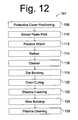
- FIG. 12is a flow chart summarizing one particular method 107 for performing camera chip mounting operation 102 of method 100 .
- protective cover positionoperation 108
- protective cover 33is positioned over camera chip 12 ( FIG. 10 ).
- protective cover 33can be positioned during lens mount overmolding operation 103 , at another point in camera chip mounting operation 102 , or omitted.
- solder paste printoperation 110 solder waste traces are printed on the individual PCBs 16 a of the substrate strip 52 .
- a “passive attach” operation 112the passive components 18 are placed on the PCBs 16 a .
- a “reflow” operation 114the substrate strip 52 is subjected to a reflow soldering operation, and in a “cleaner” operation 116 , the substrate strip 52 is subjected to conventional cleaning following the reflow soldering process 114 .
- a “die bonding” operation 118the camera chips 12 are bonded (by an adhesive in this example) to the respective PCBs 16 a .
- an “oven curing” operation 120the adhesive applied in the previous operation is cured in an oven.
- a “plasma cleaning” operation122 surfaces to which wires are to be bonded (in subsequent operations) are etched using inert gasses.
- a “wire bonding” operation 124the attachment wires 17 are bonded using thermosonic bonding.
- a second “plasma cleaning” operation 126the PCBs 16 a are again cleaned.
- FIG. 13is a flow chart summarizing one particular method 127 of performing lens mount overmolding operation 103 of method 100 .
- a protective cover positioning operation 128protective cover 33 is positioned over camera chip 12 . Note that this step is unnecessary if protective cover 33 has already been mounted as part of a prior process, or if no protective cover is desired.
- the mold chase 56is placed over the substrate strip 52 and the molding 26 is formed as previously discussed herein.
- molding 26can also serve to hold protective covering 33 in place, essentially sealing in the sensor array area 14 of camera chip 12 .
- the molding 26is formed using generally conventional “overmolding” techniques known to those skilled in the art. The mold will provide for exposure of the sensor array area 14 of the camera chip 12 after the molding operation.
- an “O/M curing” operation 130the molding 26 is briefly heat cured.
- FIG. 14is a flow chart summarizing one particular method 131 of performing device separation operation 104 of FIG. 11 .
- the protective tape 60is placed over all of the PCBs 16 a (as illustrated in FIG. 9 ) in an “attach cover tape” operation 132 .
- the individual PCBs 16 aare sawn apart. The sawing is done right through the protective tape 60 such that the resulting product is a plurality of the individual PCB assemblies 22 a , each having a respective portion of the protective tape 60 still in place thereon.
- the protective tape 60is a commonly available commodity provided for protecting components during a soldering process, and the like.
- the bits of the protective tape 60are removed from each of the PCB assemblies 22 a.
- FIG. 15is a flow chart summarizing one particular method 139 of performing lens mounting operation 105 of method 100 .
- a “lens mounting” operation 140one of the lens assemblies 24 a is inserted into each of the moldings 26 ( FIG. 10 ).
- a “focus and testing” operation 142the lens assembly 24 a is moved up and down (along the Z axis 32 of FIG. 1 ) to perfect the focus of the lens assembly 24 a in relation to the sensor array area 14 of the camera chip 12 . Correct focus is determined by generally conventional automatic testing equipment. It should be noted that the inventors believe that this operation might be eliminated in the future by referencing the position of the mold chase 56 in relation to the camera chip 12 during the “over molding” operation 128 .
- a “glue dispensing and curing” operation 144ultra violet cure adhesive 28 is applied as previously discussed herein, and then cured using ultra violet light.
- Another modificationwould be to replace the air filled gap 30 described herein with an optically clear spacer made, for example, of clear plastic, glass, or some other optically acceptable material.
- an optically clear spacermade, for example, of clear plastic, glass, or some other optically acceptable material.
- Providing a spacer which abuts both the camera chip 12 and the lens 24could eliminate the need to focus the lens during the lens mounting operation.
- secondary lensessuch as zoom lens assemblies and the like, can be fit to the already mechanically centered lens assembly 24 or 24 a .
- a spacerwould also serve as a protective cover, thereby eliminating the need to provide a separate protective cover.
- the lens assemblies 22 , 22 acould be secured to the PCB 16 , 16 a in relation to the camera chip 12 by other mechanical means, such as a mechanical clip, or the like.
- Additional components and/or partscould readily be added to the present invention.
- One possible examplewould be to provide a glass cover on the molding 26 .
- Such as covermight serve several purposes. It could protect the sensor array area 14 during storage, transport and handling, it could optionally provide a service whereby the device could be lifted by “pick-and-place” machines, and it could protect the sensor array area 14 during reflow soldering operations.
- the inventive integrated camera module 10 , 10 ais intended to be widely used for capturing visual images in very small devices such as small digital cameras, cellular telephones, and the like.
- the device and methodare appropriate to a wide variety of applications, including using sensor modules ranging from VGA resolution to 1.3 Megapixel or even greater.
- the method and apparatus described hereinare inexpensive in the molding material and process is lower in cost as compared to the attachment of a housing using conventional methods. This is mainly because the molding process will be performed on an entire panel having thereon a large number of the integrated camera modules 10 at once, rather than attaching the lenses one at a time. Also, the cost of molding compound will be lower than the cost of individual housing pieces formerly used for attaching the lenses.
- the final assembly of the integrated camera modules 10will be more robust and more accurate with respect to X and Y locations. This is accomplished by ensuring that the sensor die placement and the overmold insert locations are controlled by the same local fiducial features on the substrate.
- Current methodsinvolve use of guide pins and other means for the placement of the housing. These inherently involve greater tolerance build up compared to a mold with greater dimensional accuracy and more stable dimensions.
- Z dimension accuracywill be accomplished with reference to the camera chip 12 surface itself, which is the key reference for camera focus. It is anticipated that, in the future, this will obviate the need for active alignment in most cases. Also, the fact that the alignment is done without having to rotate the lens assembly into a threaded housing will inherently make the lens placement more stable.
- the integrated camera module 10 , 10 a of the present inventionmay be readily produced and integrated with existing design configurations for camera systems and others yet to be conceived, and since the advantages as described herein are provided, it is expected that it will be readily accepted in the industry. For these and other reasons, it is expected that the utility and industrial applicability of the invention will be both significant in scope and long-lasting in duration.
Landscapes
- Engineering & Computer Science (AREA)
- Multimedia (AREA)
- Signal Processing (AREA)
- Transforming Light Signals Into Electric Signals (AREA)
- Studio Devices (AREA)
- Solid State Image Pick-Up Elements (AREA)
- Lens Barrels (AREA)
Abstract
Description
Claims (74)
Priority Applications (11)
| Application Number | Priority Date | Filing Date | Title |
|---|---|---|---|
| US10/784,102US7872686B2 (en) | 2004-02-20 | 2004-02-20 | Integrated lens and chip assembly for a digital camera |
| TW094104486ATWI258052B (en) | 2004-02-20 | 2005-02-16 | Integrated lens and chip assembly for a digital camera |
| PCT/US2005/005139WO2005081853A2 (en) | 2004-02-20 | 2005-02-18 | Integrated lens and chip assembly for a digital camera |
| CNA2005800089902ACN101124813A (en) | 2004-02-20 | 2005-02-18 | Integrated lens and chip assembly for digital camera |
| JP2006554218AJP2007523568A (en) | 2004-02-20 | 2005-02-18 | Integrated lens and chip assembly for digital cameras |
| EP10177430AEP2265000A1 (en) | 2004-02-20 | 2005-02-18 | Method for manufacturing camera modules and substrate comprising a plurality of camera integrated circuit chips |
| CN2009101706321ACN101656218B (en) | 2004-02-20 | 2005-02-18 | Method for producing camera module and corresponding substrate |
| CA002556477ACA2556477A1 (en) | 2004-02-20 | 2005-02-18 | Integrated lens and chip assembly for a digital camera |
| EP05713765AEP1726157A4 (en) | 2004-02-20 | 2005-02-18 | Integrated lens and chip assembly for a digital camera |
| US11/247,993US7796187B2 (en) | 2004-02-20 | 2005-10-11 | Wafer based camera module and method of manufacture |
| US12/930,822US8477239B2 (en) | 2004-02-20 | 2011-01-18 | Integrated lens and chip assembly for a digital camera |
Applications Claiming Priority (1)
| Application Number | Priority Date | Filing Date | Title |
|---|---|---|---|
| US10/784,102US7872686B2 (en) | 2004-02-20 | 2004-02-20 | Integrated lens and chip assembly for a digital camera |
Related Child Applications (2)
| Application Number | Title | Priority Date | Filing Date |
|---|---|---|---|
| US11/247,993Continuation-In-PartUS7796187B2 (en) | 2004-02-20 | 2005-10-11 | Wafer based camera module and method of manufacture |
| US12/930,822ContinuationUS8477239B2 (en) | 2004-02-20 | 2011-01-18 | Integrated lens and chip assembly for a digital camera |
Publications (2)
| Publication Number | Publication Date |
|---|---|
| US20050185088A1 US20050185088A1 (en) | 2005-08-25 |
| US7872686B2true US7872686B2 (en) | 2011-01-18 |
Family
ID=34861402
Family Applications (2)
| Application Number | Title | Priority Date | Filing Date |
|---|---|---|---|
| US10/784,102Expired - Fee RelatedUS7872686B2 (en) | 2004-02-20 | 2004-02-20 | Integrated lens and chip assembly for a digital camera |
| US12/930,822Expired - Fee RelatedUS8477239B2 (en) | 2004-02-20 | 2011-01-18 | Integrated lens and chip assembly for a digital camera |
Family Applications After (1)
| Application Number | Title | Priority Date | Filing Date |
|---|---|---|---|
| US12/930,822Expired - Fee RelatedUS8477239B2 (en) | 2004-02-20 | 2011-01-18 | Integrated lens and chip assembly for a digital camera |
Country Status (7)
| Country | Link |
|---|---|
| US (2) | US7872686B2 (en) |
| EP (2) | EP1726157A4 (en) |
| JP (1) | JP2007523568A (en) |
| CN (2) | CN101656218B (en) |
| CA (1) | CA2556477A1 (en) |
| TW (1) | TWI258052B (en) |
| WO (1) | WO2005081853A2 (en) |
Cited By (6)
| Publication number | Priority date | Publication date | Assignee | Title |
|---|---|---|---|---|
| US20060098119A1 (en)* | 2004-11-05 | 2006-05-11 | Lg Electronics Inc. | Mobile terminal |
| US20100307253A1 (en)* | 2006-09-15 | 2010-12-09 | Robert Bosch Gmbh | Pressure sensor for side-impact sensing and method for forming a surface of a protective material for a pressure sensor |
| US20110026919A1 (en)* | 2009-07-29 | 2011-02-03 | Avago Technologies Fiber Ip (Singapore) Pte. Ltd. | Half-duplex, single-fiber (s-f) optical transceiver module and method |
| US20110115974A1 (en)* | 2004-02-20 | 2011-05-19 | Vidyadhar Sitaram Kale | Integrated lens and chip assembly for a digital camera |
| US20140212086A1 (en)* | 2013-01-28 | 2014-07-31 | Hitachi Metals, Ltd. | Optical module |
| US9178093B2 (en) | 2011-07-06 | 2015-11-03 | Flextronics Ap, Llc | Solar cell module on molded lead-frame and method of manufacture |
Families Citing this family (50)
| Publication number | Priority date | Publication date | Assignee | Title |
|---|---|---|---|---|
| JP2005101711A (en)* | 2003-09-22 | 2005-04-14 | Renesas Technology Corp | Solid-state imaging device and manufacturing method thereof |
| US7796187B2 (en)* | 2004-02-20 | 2010-09-14 | Flextronics Ap Llc | Wafer based camera module and method of manufacture |
| JP2005284147A (en)* | 2004-03-30 | 2005-10-13 | Fuji Photo Film Co Ltd | Imaging device |
| US20050264690A1 (en)* | 2004-05-28 | 2005-12-01 | Tekom Technologies, Inc. | Image sensor |
| EP1769719A4 (en)* | 2004-07-05 | 2009-10-21 | Olympus Medical Systems Corp | ELECTRONIC ENDOSCOPE |
| JP4852535B2 (en)* | 2005-04-01 | 2012-01-11 | パナソニック株式会社 | Imaging device |
| US7288757B2 (en)* | 2005-09-01 | 2007-10-30 | Micron Technology, Inc. | Microelectronic imaging devices and associated methods for attaching transmissive elements |
| US7531773B2 (en) | 2005-09-08 | 2009-05-12 | Flextronics Ap, Llc | Auto-focus and zoom module having a lead screw with its rotation results in translation of an optics group |
| US7469100B2 (en) | 2005-10-03 | 2008-12-23 | Flextronics Ap Llc | Micro camera module with discrete manual focal positions |
| DE102006013164A1 (en)* | 2006-03-22 | 2007-09-27 | Robert Bosch Gmbh | Method for mounting a camera module and camera module |
| US20070236591A1 (en)* | 2006-04-11 | 2007-10-11 | Tam Samuel W | Method for mounting protective covers over image capture devices and devices manufactured thereby |
| US8092102B2 (en)* | 2006-05-31 | 2012-01-10 | Flextronics Ap Llc | Camera module with premolded lens housing and method of manufacture |
| US7983556B2 (en)* | 2006-11-03 | 2011-07-19 | Flextronics Ap Llc | Camera module with contamination reduction feature |
| US8456560B2 (en)* | 2007-01-26 | 2013-06-04 | Digitaloptics Corporation | Wafer level camera module and method of manufacture |
| CA2685080A1 (en) | 2007-04-24 | 2008-11-06 | Flextronics Ap Llc | Small form factor modules using wafer level optics with bottom cavity and flip-chip assembly |
| US8488046B2 (en)* | 2007-12-27 | 2013-07-16 | Digitaloptics Corporation | Configurable tele wide module |
| US9118825B2 (en)* | 2008-02-22 | 2015-08-25 | Nan Chang O-Film Optoelectronics Technology Ltd. | Attachment of wafer level optics |
| WO2010091347A1 (en)* | 2009-02-06 | 2010-08-12 | Magna Electronics Inc. | Improvements to camera for vehicle |
| JP5487842B2 (en)* | 2009-06-23 | 2014-05-14 | ソニー株式会社 | Solid-state imaging device |
| US9419032B2 (en)* | 2009-08-14 | 2016-08-16 | Nanchang O-Film Optoelectronics Technology Ltd | Wafer level camera module with molded housing and method of manufacturing |
| US8760571B2 (en) | 2009-09-21 | 2014-06-24 | Microsoft Corporation | Alignment of lens and image sensor |
| US10782187B2 (en)* | 2010-07-08 | 2020-09-22 | Cvg Management Corporation | Infrared temperature measurement and stabilization thereof |
| KR20120079551A (en)* | 2011-01-05 | 2012-07-13 | 엘지이노텍 주식회사 | Focus free camera module |
| US8545114B2 (en) | 2011-03-11 | 2013-10-01 | Digitaloptics Corporation | Auto focus-zoom actuator or camera module contamination reduction feature with integrated protective membrane |
| WO2013079705A1 (en)* | 2011-11-30 | 2013-06-06 | Anteryon International Bv | Apparatus and method |
| JP2014138119A (en)* | 2013-01-17 | 2014-07-28 | Sony Corp | Semiconductor device and semiconductor device manufacturing method |
| CN104376616A (en)* | 2013-08-16 | 2015-02-25 | 深圳富泰宏精密工业有限公司 | Automobile data recorder |
| TWI650016B (en) | 2013-08-22 | 2019-02-01 | 新力股份有限公司 | Imaging device, manufacturing method and electronic device |
| US9258467B2 (en)* | 2013-11-19 | 2016-02-09 | Stmicroelectronics Pte Ltd. | Camera module |
| US9467606B2 (en)* | 2014-06-10 | 2016-10-11 | Omnivision Technologies, Inc. | Wafer level stepped sensor holder |
| CN104916008A (en)* | 2015-06-26 | 2015-09-16 | 深圳市安视达电子科技有限公司 | Automobile data recorder |
| US10447900B2 (en)* | 2015-08-06 | 2019-10-15 | Apple Inc. | Camera module design with lead frame and plastic moulding |
| KR102465474B1 (en)* | 2016-02-18 | 2022-11-09 | 닝보 써니 오포테크 코., 엘티디. | Integral packaging process-based camera module, integral base component of same, and manufacturing method therefor |
| KR102335306B1 (en)* | 2016-03-12 | 2021-12-03 | 닝보 써니 오포테크 코., 엘티디. | Array Imaging Module and Molded Photensitive Assembly and Manufacturing Method Thereof for Electronic Device |
| US10750071B2 (en)* | 2016-03-12 | 2020-08-18 | Ningbo Sunny Opotech Co., Ltd. | Camera module with lens array arrangement, circuit board assembly, and image sensor and manufacturing method thereof |
| EP3446338A4 (en)* | 2016-03-23 | 2019-06-05 | AMS Sensors Singapore Pte. Ltd. | Optoelectronic module assembly and manufacturing method |
| CN107466160B (en) | 2016-06-06 | 2022-04-29 | 宁波舜宇光电信息有限公司 | Equipment and method for manufacturing molded circuit board of camera module |
| CN107466159B (en) | 2016-06-06 | 2022-07-19 | 宁波舜宇光电信息有限公司 | Molded circuit board of camera module and its manufacturing equipment and manufacturing method |
| KR101785458B1 (en)* | 2016-06-07 | 2017-10-16 | 엘지전자 주식회사 | Camera module and mobile terminal having the same |
| KR102405359B1 (en)* | 2017-02-08 | 2022-06-07 | 닝보 써니 오포테크 코., 엘티디. | Photographing module and mold photosensitive assembly and manufacturing method thereof, and electronic device |
| CN108461510A (en)* | 2017-02-22 | 2018-08-28 | 深圳市中兴微电子技术有限公司 | A kind of camera module and preparation method thereof |
| CN106998417A (en)* | 2017-03-24 | 2017-08-01 | 谢超 | Miniature video camera module manufacture craft |
| CN110914753A (en)* | 2017-07-31 | 2020-03-24 | 日本电产株式会社 | Light-blocking blade, blade drive device, and imaging device |
| CN110945424A (en)* | 2017-07-31 | 2020-03-31 | 日本电产株式会社 | Light-blocking blade, blade drive device, and imaging device |
| WO2019026449A1 (en)* | 2017-07-31 | 2019-02-07 | 日本電産株式会社 | Light-shielding blade, blade drive device, and imaging device |
| CN110475049B (en)* | 2018-05-11 | 2022-03-15 | 三星电机株式会社 | Camera module and method of manufacturing the same |
| CN110611754A (en)* | 2018-06-15 | 2019-12-24 | 三赢科技(深圳)有限公司 | camera module |
| JP7641740B2 (en) | 2018-07-06 | 2025-03-07 | 浜松ホトニクス株式会社 | Spectroscopic module and method for manufacturing the same |
| US20210321025A1 (en)* | 2018-08-21 | 2021-10-14 | Ningbo Sunny Opotech Co., Ltd. | Camera module and molded photosensitive assembly and manufacturing methods thereof, and electronic device |
| US11094858B2 (en)* | 2019-08-01 | 2021-08-17 | Advanced Semiconductor Engineering, Inc. | Tape, encapsulating process and optical device |
Citations (41)
| Publication number | Priority date | Publication date | Assignee | Title |
|---|---|---|---|---|
| US4894707A (en) | 1987-02-12 | 1990-01-16 | Mitsubishi Denki Kabushiki Kaisha | Semiconductor device having a light transparent window and a method of producing same |
| EP0813236A1 (en) | 1996-06-11 | 1997-12-17 | European Semiconductor Assembly (Eurasem) B.V. | Method for encapsulating an integrated semi-conductor circuit |
| US6122009A (en) | 1995-05-31 | 2000-09-19 | Sony Corporation | Image pickup apparatus fabrication method thereof image pickup adaptor apparatus signal processing apparatus signal processing method thereof information processing apparatus and information processing method |
| JP2001292365A (en) | 2000-04-07 | 2001-10-19 | Mitsubishi Electric Corp | Imaging device and method of manufacturing the same |
| US6384397B1 (en) | 2000-05-10 | 2002-05-07 | National Semiconductor Corporation | Low cost die sized module for imaging application having a lens housing assembly |
| US6414299B1 (en) | 1999-02-17 | 2002-07-02 | Canon Kabushiki Kaisha | Method of mounting optical sensor package |
| JP2002252796A (en) | 2001-02-26 | 2002-09-06 | Mitsubishi Electric Corp | Imaging device |
| US6476417B2 (en)* | 2000-10-19 | 2002-11-05 | Fujitsu Limited | Image-pickup semiconductor device having a lens, a light-receiving element and a flexible substrate therebetween with a shading plate blocking undesired light rays |
| US20020167605A1 (en) | 2001-05-09 | 2002-11-14 | Kazuo Akimoto | Photographing apparatus |
| US20020191103A1 (en)* | 2001-06-05 | 2002-12-19 | Kazuo Akimoto | Solid photographing apparatus |
| JP2003078077A (en) | 2001-09-05 | 2003-03-14 | Sanyo Electric Co Ltd | The camera module |
| US20030071342A1 (en) | 2001-02-28 | 2003-04-17 | Fujitsu Limited | Semiconductor device and method for making the same |
| JP2003131112A (en) | 2001-10-29 | 2003-05-08 | Fujitsu Ltd | Camera module and manufacturing method thereof |
| US20030137595A1 (en)* | 1997-05-16 | 2003-07-24 | Taizo Takachi | Image pickup device and camera |
| JP2003219284A (en) | 2002-01-24 | 2003-07-31 | Fujitsu Ltd | Camera module and manufacturing method thereof |
| US20030146998A1 (en)* | 2000-08-11 | 2003-08-07 | Elko Doering | Small-size imaging apparatus, in particular photographic appliance or camera |
| US20040012698A1 (en)* | 2001-03-05 | 2004-01-22 | Yasuo Suda | Image pickup model and image pickup device |
| US6686588B1 (en) | 2001-01-16 | 2004-02-03 | Amkor Technology, Inc. | Optical module with lens integral holder |
| US20040027687A1 (en) | 2002-07-03 | 2004-02-12 | Wilfried Bittner | Compact zoom lens barrel and system |
| WO2004027880A2 (en) | 2002-09-17 | 2004-04-01 | Koninklijke Philips Electronics N.V. | Camera device, method of manufacturing a camera device, wafer scale package |
| US6734419B1 (en) | 2001-06-28 | 2004-05-11 | Amkor Technology, Inc. | Method for forming an image sensor package with vision die in lens housing |
| US6741405B1 (en) | 2003-03-27 | 2004-05-25 | Exquisite Optical Technology Co., Ltd | Hood for a digital image collecting lens |
| US20040109079A1 (en)* | 2002-05-13 | 2004-06-10 | Rohm Co., Ltd. | Image sensor module and method of making the same |
| EP1429168A2 (en) | 2002-12-13 | 2004-06-16 | Konica Minolta Holdings, Inc. | Image sensing device and portable terminal |
| US20040189853A1 (en)* | 2001-08-07 | 2004-09-30 | Takashi Takeuchi | Camera module |
| US20050046740A1 (en) | 2003-08-29 | 2005-03-03 | Davis Raymond A.. | Apparatus including a dual camera module and method of using the same |
| US20050212947A1 (en) | 2004-03-26 | 2005-09-29 | Fuji Photo Film Co., Ltd. | Image capture apparatus |
| US20050274883A1 (en) | 2004-06-11 | 2005-12-15 | Canon Kabushiki Kaisha | Imaging and electronic apparatus |
| US20050285016A1 (en) | 2004-06-29 | 2005-12-29 | Yung-Cheol Kong | Image sensor module structure comprising wire bonding package and method of manufacturing the image sensor module structure |
| US20060006486A1 (en) | 2004-06-10 | 2006-01-12 | Byoung-Rim Seo | Image sensor package and method of manufacturing the same |
| US20060028573A1 (en) | 2004-08-06 | 2006-02-09 | Byoung-Rim Seo | Image sensor camera module and method of fabricating the same |
| US7061106B2 (en) | 2004-04-28 | 2006-06-13 | Advanced Chip Engineering Technology Inc. | Structure of image sensor module and a method for manufacturing of wafer level package |
| US20060132644A1 (en) | 2004-02-20 | 2006-06-22 | Dongkai Shangguan | Wafer based camera module and method of manufacture |
| US7091571B1 (en) | 2003-12-11 | 2006-08-15 | Amkor Technology, Inc. | Image sensor package and method for manufacture thereof |
| US7122787B2 (en)* | 2003-05-09 | 2006-10-17 | Matsushita Electric Industrial Co., Ltd. | Imaging apparatus with three dimensional circuit board |
| US20070058069A1 (en) | 2005-09-14 | 2007-03-15 | Po-Hung Chen | Packaging structure of a light sensation module |
| US7199438B2 (en)* | 2003-09-23 | 2007-04-03 | Advanced Semiconductor Engineering, Inc. | Overmolded optical package |
| US20070278394A1 (en) | 2006-05-31 | 2007-12-06 | Dongkai Shangguan | Camera module with premolded lens housing and method of manufacture |
| US7579583B2 (en) | 2003-12-02 | 2009-08-25 | Samsung Electronics Co., Ltd. | Solid-state imaging apparatus, wiring substrate and methods of manufacturing the same |
| US7583309B2 (en) | 2002-06-28 | 2009-09-01 | Kyocera Coproration | Imaging device package camera module and camera module producing method |
| US7679669B2 (en) | 2006-05-18 | 2010-03-16 | Samsung Electro-Mechanics Co., Ltd. | Camera module package |
Family Cites Families (13)
| Publication number | Priority date | Publication date | Assignee | Title |
|---|---|---|---|---|
| US5617131A (en)* | 1993-10-28 | 1997-04-01 | Kyocera Corporation | Image device having a spacer with image arrays disposed in holes thereof |
| JP3247384B2 (en)* | 1994-03-18 | 2002-01-15 | 日立化成工業株式会社 | Semiconductor package manufacturing method and semiconductor package |
| US6483101B1 (en)* | 1999-12-08 | 2002-11-19 | Amkor Technology, Inc. | Molded image sensor package having lens holder |
| JP2001188155A (en) | 1999-12-28 | 2001-07-10 | Kuurii Components Kk | Image sensor fixing means |
| JP3725012B2 (en)* | 2000-08-17 | 2005-12-07 | シャープ株式会社 | Manufacturing method of lens-integrated solid-state imaging device |
| DE10109787A1 (en)* | 2001-02-28 | 2002-10-02 | Infineon Technologies Ag | Digital camera with a light-sensitive sensor |
| JP4647851B2 (en) | 2001-08-07 | 2011-03-09 | 日立マクセル株式会社 | The camera module |
| US7304362B2 (en)* | 2002-05-20 | 2007-12-04 | Stmicroelectronics, Inc. | Molded integrated circuit package with exposed active area |
| JP2004200965A (en) | 2002-12-18 | 2004-07-15 | Sanyo Electric Co Ltd | Camera module and manufacturing method thereof |
| JP2004296453A (en)* | 2003-02-06 | 2004-10-21 | Sharp Corp | Solid-state imaging device, semiconductor wafer, module for optical device, method for manufacturing solid-state imaging device, and method for manufacturing module for optical device |
| JP2005210628A (en) | 2004-01-26 | 2005-08-04 | Mitsui Chemicals Inc | Substrate for mounting semiconductor for imaging device, and imaging device |
| US7872686B2 (en) | 2004-02-20 | 2011-01-18 | Flextronics International Usa, Inc. | Integrated lens and chip assembly for a digital camera |
| JP2006053232A (en) | 2004-08-10 | 2006-02-23 | Sony Corp | Electronic imaging device |
- 2004
- 2004-02-20USUS10/784,102patent/US7872686B2/ennot_activeExpired - Fee Related
- 2005
- 2005-02-16TWTW094104486Apatent/TWI258052B/ennot_activeIP Right Cessation
- 2005-02-18EPEP05713765Apatent/EP1726157A4/ennot_activeWithdrawn
- 2005-02-18CNCN2009101706321Apatent/CN101656218B/ennot_activeExpired - Lifetime
- 2005-02-18EPEP10177430Apatent/EP2265000A1/ennot_activeWithdrawn
- 2005-02-18CNCNA2005800089902Apatent/CN101124813A/enactivePending
- 2005-02-18WOPCT/US2005/005139patent/WO2005081853A2/enactiveApplication Filing
- 2005-02-18JPJP2006554218Apatent/JP2007523568A/enactivePending
- 2005-02-18CACA002556477Apatent/CA2556477A1/ennot_activeAbandoned
- 2011
- 2011-01-18USUS12/930,822patent/US8477239B2/ennot_activeExpired - Fee Related
Patent Citations (45)
| Publication number | Priority date | Publication date | Assignee | Title |
|---|---|---|---|---|
| US4894707A (en) | 1987-02-12 | 1990-01-16 | Mitsubishi Denki Kabushiki Kaisha | Semiconductor device having a light transparent window and a method of producing same |
| US6122009A (en) | 1995-05-31 | 2000-09-19 | Sony Corporation | Image pickup apparatus fabrication method thereof image pickup adaptor apparatus signal processing apparatus signal processing method thereof information processing apparatus and information processing method |
| EP0813236A1 (en) | 1996-06-11 | 1997-12-17 | European Semiconductor Assembly (Eurasem) B.V. | Method for encapsulating an integrated semi-conductor circuit |
| US20030137595A1 (en)* | 1997-05-16 | 2003-07-24 | Taizo Takachi | Image pickup device and camera |
| US6414299B1 (en) | 1999-02-17 | 2002-07-02 | Canon Kabushiki Kaisha | Method of mounting optical sensor package |
| JP2001292365A (en) | 2000-04-07 | 2001-10-19 | Mitsubishi Electric Corp | Imaging device and method of manufacturing the same |
| US6384397B1 (en) | 2000-05-10 | 2002-05-07 | National Semiconductor Corporation | Low cost die sized module for imaging application having a lens housing assembly |
| US20030146998A1 (en)* | 2000-08-11 | 2003-08-07 | Elko Doering | Small-size imaging apparatus, in particular photographic appliance or camera |
| US6476417B2 (en)* | 2000-10-19 | 2002-11-05 | Fujitsu Limited | Image-pickup semiconductor device having a lens, a light-receiving element and a flexible substrate therebetween with a shading plate blocking undesired light rays |
| US6686588B1 (en) | 2001-01-16 | 2004-02-03 | Amkor Technology, Inc. | Optical module with lens integral holder |
| JP2002252796A (en) | 2001-02-26 | 2002-09-06 | Mitsubishi Electric Corp | Imaging device |
| US7009654B2 (en)* | 2001-02-26 | 2006-03-07 | Mitsubishi Denki Kabushiki Kaisha | Image pickup apparatus |
| US20020145676A1 (en) | 2001-02-26 | 2002-10-10 | Tetsuya Kuno | Image pickup apparatus |
| US20030071342A1 (en) | 2001-02-28 | 2003-04-17 | Fujitsu Limited | Semiconductor device and method for making the same |
| US6798031B2 (en)* | 2001-02-28 | 2004-09-28 | Fujitsu Limited | Semiconductor device and method for making the same |
| US20040012698A1 (en)* | 2001-03-05 | 2004-01-22 | Yasuo Suda | Image pickup model and image pickup device |
| US20020167605A1 (en) | 2001-05-09 | 2002-11-14 | Kazuo Akimoto | Photographing apparatus |
| US20020191103A1 (en)* | 2001-06-05 | 2002-12-19 | Kazuo Akimoto | Solid photographing apparatus |
| US6734419B1 (en) | 2001-06-28 | 2004-05-11 | Amkor Technology, Inc. | Method for forming an image sensor package with vision die in lens housing |
| US20040189853A1 (en)* | 2001-08-07 | 2004-09-30 | Takashi Takeuchi | Camera module |
| JP2003078077A (en) | 2001-09-05 | 2003-03-14 | Sanyo Electric Co Ltd | The camera module |
| JP2003131112A (en) | 2001-10-29 | 2003-05-08 | Fujitsu Ltd | Camera module and manufacturing method thereof |
| JP2003219284A (en) | 2002-01-24 | 2003-07-31 | Fujitsu Ltd | Camera module and manufacturing method thereof |
| US20040109079A1 (en)* | 2002-05-13 | 2004-06-10 | Rohm Co., Ltd. | Image sensor module and method of making the same |
| US7583309B2 (en) | 2002-06-28 | 2009-09-01 | Kyocera Coproration | Imaging device package camera module and camera module producing method |
| US20040027687A1 (en) | 2002-07-03 | 2004-02-12 | Wilfried Bittner | Compact zoom lens barrel and system |
| US20060044450A1 (en) | 2002-09-17 | 2006-03-02 | Koninklijke Philips Electronics, N.C. | Camera device, method of manufacturing a camera device, wafer scale package |
| WO2004027880A2 (en) | 2002-09-17 | 2004-04-01 | Koninklijke Philips Electronics N.V. | Camera device, method of manufacturing a camera device, wafer scale package |
| EP1429168A2 (en) | 2002-12-13 | 2004-06-16 | Konica Minolta Holdings, Inc. | Image sensing device and portable terminal |
| US6741405B1 (en) | 2003-03-27 | 2004-05-25 | Exquisite Optical Technology Co., Ltd | Hood for a digital image collecting lens |
| US7122787B2 (en)* | 2003-05-09 | 2006-10-17 | Matsushita Electric Industrial Co., Ltd. | Imaging apparatus with three dimensional circuit board |
| US20050046740A1 (en) | 2003-08-29 | 2005-03-03 | Davis Raymond A.. | Apparatus including a dual camera module and method of using the same |
| US7199438B2 (en)* | 2003-09-23 | 2007-04-03 | Advanced Semiconductor Engineering, Inc. | Overmolded optical package |
| US7579583B2 (en) | 2003-12-02 | 2009-08-25 | Samsung Electronics Co., Ltd. | Solid-state imaging apparatus, wiring substrate and methods of manufacturing the same |
| US7091571B1 (en) | 2003-12-11 | 2006-08-15 | Amkor Technology, Inc. | Image sensor package and method for manufacture thereof |
| US20060132644A1 (en) | 2004-02-20 | 2006-06-22 | Dongkai Shangguan | Wafer based camera module and method of manufacture |
| US20050212947A1 (en) | 2004-03-26 | 2005-09-29 | Fuji Photo Film Co., Ltd. | Image capture apparatus |
| US7061106B2 (en) | 2004-04-28 | 2006-06-13 | Advanced Chip Engineering Technology Inc. | Structure of image sensor module and a method for manufacturing of wafer level package |
| US20060006486A1 (en) | 2004-06-10 | 2006-01-12 | Byoung-Rim Seo | Image sensor package and method of manufacturing the same |
| US20050274883A1 (en) | 2004-06-11 | 2005-12-15 | Canon Kabushiki Kaisha | Imaging and electronic apparatus |
| US20050285016A1 (en) | 2004-06-29 | 2005-12-29 | Yung-Cheol Kong | Image sensor module structure comprising wire bonding package and method of manufacturing the image sensor module structure |
| US20060028573A1 (en) | 2004-08-06 | 2006-02-09 | Byoung-Rim Seo | Image sensor camera module and method of fabricating the same |
| US20070058069A1 (en) | 2005-09-14 | 2007-03-15 | Po-Hung Chen | Packaging structure of a light sensation module |
| US7679669B2 (en) | 2006-05-18 | 2010-03-16 | Samsung Electro-Mechanics Co., Ltd. | Camera module package |
| US20070278394A1 (en) | 2006-05-31 | 2007-12-06 | Dongkai Shangguan | Camera module with premolded lens housing and method of manufacture |
Non-Patent Citations (26)
| Title |
|---|
| CN Application No. 20058008990.2, Office Action dated Aug. 1, 2008 (English translation). |
| CN Application No. 20058008990.2, Office Action dated Jun. 12, 2009 (English translation). |
| CN Application No. 200680046525.2, Office Action dated Jul. 10, 2009 (English translation). |
| CN Application No. 200680046525.2, Office Action dated Mar. 25, 2010. |
| CN Application No. 200780026542.4, Office Action dated Nov. 13, 2009 (English translation). |
| EP Application No. 05 713 765.5-2202, Office Action dated Feb. 25, 2010. |
| EP Application No. 05 713 765.5-2202, Office Action dated Mar. 17, 2009. |
| EP Application No. 05 713 765.5-2202, Supplementary European Search Report dated Dec. 5, 2008. |
| EP Application No. 06 816 608.1-1241, Extended European Search Report dated Mar. 10, 2010. |
| http://zenith.czechtrade.us/acrylic-glass, 2007.* |
| JP Application No. 2006-554218, Office Action dated Dec. 3, 2009. |
| JP Application No. 2006-554218, Office Action dated Jul. 28, 2010. |
| PCT Application No. PCT/US2005/005139, International Preliminary Report on Patentability dated Jul. 19, 2007. |
| PCT Application No. PCT/US2005/005139, International Search Report and Written Opinion dated Jun. 12, 2007. |
| PCT Application No. PCT/US2006/039521, International Preliminary Report on Patentability dated Apr. 24, 2008. |
| PCT Application No. PCT/US2006/039521, International Search Report and Written Opinion dated Aug. 2, 2007. |
| PCT Application No. PCT/US2007/013014, International Preliminary Report on Patentability dated Dec. 18, 2009. |
| PCT Application No. PCT/US2007/013014, International Search Report and Written Opinion dated Aug. 27, 2008. |
| U.S. Appl. No. 11/247,993, Notice of Allowance dated May 4, 2010. |
| U.S. Appl. No. 11/247,993, Office Action dated Dec. 26, 2008. |
| U.S. Appl. No. 11/247,993, Office Action dated Jan. 6, 2010. |
| U.S. Appl. No. 11/247,993, Office Action dated Sep. 10, 2009. |
| U.S. Appl. No. 11/444,277, Office Action dated Aug. 3, 2010. |
| U.S. Appl. No. 11/444,277, Office Action dated Aug. 5, 2008. |
| U.S. Appl. No. 11/444,277, Office Action dated May 7, 2009. |
| U.S. Appl. No. 11/444,277, Office Action dated Nov. 18, 2009. |
Cited By (10)
| Publication number | Priority date | Publication date | Assignee | Title |
|---|---|---|---|---|
| US20110115974A1 (en)* | 2004-02-20 | 2011-05-19 | Vidyadhar Sitaram Kale | Integrated lens and chip assembly for a digital camera |
| US8477239B2 (en)* | 2004-02-20 | 2013-07-02 | Digitaloptics Corporation | Integrated lens and chip assembly for a digital camera |
| US20060098119A1 (en)* | 2004-11-05 | 2006-05-11 | Lg Electronics Inc. | Mobile terminal |
| US20100307253A1 (en)* | 2006-09-15 | 2010-12-09 | Robert Bosch Gmbh | Pressure sensor for side-impact sensing and method for forming a surface of a protective material for a pressure sensor |
| US8353214B2 (en)* | 2006-09-15 | 2013-01-15 | Robert Bosch Gmbh | Pressure sensor for side-impact sensing and method for forming a surface of a protective material for a pressure sensor |
| US20110026919A1 (en)* | 2009-07-29 | 2011-02-03 | Avago Technologies Fiber Ip (Singapore) Pte. Ltd. | Half-duplex, single-fiber (s-f) optical transceiver module and method |
| US8265487B2 (en)* | 2009-07-29 | 2012-09-11 | Avago Technologies Fiber Ip (Singapore) Pte. Ltd. | Half-duplex, single-fiber (S-F) optical transceiver module and method |
| US9178093B2 (en) | 2011-07-06 | 2015-11-03 | Flextronics Ap, Llc | Solar cell module on molded lead-frame and method of manufacture |
| US20140212086A1 (en)* | 2013-01-28 | 2014-07-31 | Hitachi Metals, Ltd. | Optical module |
| US9104000B2 (en)* | 2013-01-28 | 2015-08-11 | Hitachi Metals, Ltd. | Optical module |
Also Published As
| Publication number | Publication date |
|---|---|
| US8477239B2 (en) | 2013-07-02 |
| US20050185088A1 (en) | 2005-08-25 |
| EP2265000A1 (en) | 2010-12-22 |
| CA2556477A1 (en) | 2005-09-09 |
| CN101656218B (en) | 2012-02-08 |
| EP1726157A4 (en) | 2009-01-07 |
| CN101656218A (en) | 2010-02-24 |
| CN101124813A (en) | 2008-02-13 |
| TWI258052B (en) | 2006-07-11 |
| JP2007523568A (en) | 2007-08-16 |
| TW200530731A (en) | 2005-09-16 |
| WO2005081853A2 (en) | 2005-09-09 |
| EP1726157A2 (en) | 2006-11-29 |
| WO2005081853A3 (en) | 2007-08-02 |
| US20110115974A1 (en) | 2011-05-19 |
Similar Documents
| Publication | Publication Date | Title |
|---|---|---|
| US7872686B2 (en) | Integrated lens and chip assembly for a digital camera | |
| US7796187B2 (en) | Wafer based camera module and method of manufacture | |
| CN102577644B (en) | Wafer-level camera module with molded housing and manufacturing method | |
| US7964945B2 (en) | Glass cap molding package, manufacturing method thereof and camera module | |
| JP6054344B2 (en) | Mounting wafer level optics | |
| CN100423562C (en) | Optical Device Module | |
| TWI270707B (en) | Module for optical devices, and manufacturing method of module for optical devices | |
| CA2654422C (en) | Camera module with premolded lens housing and method of manufacture | |
| US9004132B2 (en) | Apparatus and method for manufacturing camera module | |
| CN101310381A (en) | Semiconductor package and manufacturing method thereof, semiconductor module and electronic device | |
| CN102984442B (en) | Stent-type image sensing module and preparation method thereof and multi-cam device | |
| JP4017908B2 (en) | camera | |
| JP3682416B2 (en) | Method for aligning optical element and lens assembly | |
| KR101063167B1 (en) | Infrared cut filter attaching device and attaching method using same | |
| KR100927423B1 (en) | Glass cap molding package and manufacturing method thereof, and camera module |
Legal Events
| Date | Code | Title | Description |
|---|---|---|---|
| AS | Assignment | Owner name:FLEXTRONICS INTERNATIONAL USA, INC., CALIFORNIA Free format text:ASSIGNMENT OF ASSIGNORS INTEREST;ASSIGNORS:KALE, VIDYADHAR SITARAM;TAM, SAMUEL WAISING;SHANGGUAN, DONGKAI;REEL/FRAME:015020/0711 Effective date:20040218 | |
| STCF | Information on status: patent grant | Free format text:PATENTED CASE | |
| AS | Assignment | Owner name:DIGITALOPTICS CORPORATION, CALIFORNIA Free format text:ASSIGNMENT OF ASSIGNORS INTEREST;ASSIGNOR:FLEXTRONICS INTERNATIONAL USA, INC.;REEL/FRAME:028942/0876 Effective date:20120628 | |
| FPAY | Fee payment | Year of fee payment:4 | |
| AS | Assignment | Owner name:NAN CHANG O-FILM OPTOELECTRONICS TECHNOLOGY LTD, C Free format text:ASSIGNMENT OF ASSIGNORS INTEREST;ASSIGNORS:DIGITALOPTICS CORPORATION;DIGITALOPTICS CORPORATION MEMS;FOTONATION LIMITED;REEL/FRAME:034883/0237 Effective date:20141114 | |
| MAFP | Maintenance fee payment | Free format text:PAYMENT OF MAINTENANCE FEE, 8TH YEAR, LARGE ENTITY (ORIGINAL EVENT CODE: M1552) Year of fee payment:8 | |
| FEPP | Fee payment procedure | Free format text:MAINTENANCE FEE REMINDER MAILED (ORIGINAL EVENT CODE: REM.); ENTITY STATUS OF PATENT OWNER: LARGE ENTITY | |
| LAPS | Lapse for failure to pay maintenance fees | Free format text:PATENT EXPIRED FOR FAILURE TO PAY MAINTENANCE FEES (ORIGINAL EVENT CODE: EXP.); ENTITY STATUS OF PATENT OWNER: LARGE ENTITY | |
| STCH | Information on status: patent discontinuation | Free format text:PATENT EXPIRED DUE TO NONPAYMENT OF MAINTENANCE FEES UNDER 37 CFR 1.362 | |
| FP | Lapsed due to failure to pay maintenance fee | Effective date:20230118 |