US7872344B2 - Microelectronic assemblies having compliant layers - Google Patents
Microelectronic assemblies having compliant layersDownload PDFInfo
- Publication number
- US7872344B2 US7872344B2US11/474,199US47419906AUS7872344B2US 7872344 B2US7872344 B2US 7872344B2US 47419906 AUS47419906 AUS 47419906AUS 7872344 B2US7872344 B2US 7872344B2
- Authority
- US
- United States
- Prior art keywords
- chip
- compliant layer
- assembly
- layer
- contacts
- Prior art date
- Legal status (The legal status is an assumption and is not a legal conclusion. Google has not performed a legal analysis and makes no representation as to the accuracy of the status listed.)
- Expired - Fee Related
Links
Images


Classifications
- H—ELECTRICITY
- H01—ELECTRIC ELEMENTS
- H01L—SEMICONDUCTOR DEVICES NOT COVERED BY CLASS H10
- H01L23/00—Details of semiconductor or other solid state devices
- H01L23/28—Encapsulations, e.g. encapsulating layers, coatings, e.g. for protection
- H01L23/31—Encapsulations, e.g. encapsulating layers, coatings, e.g. for protection characterised by the arrangement or shape
- H01L23/3107—Encapsulations, e.g. encapsulating layers, coatings, e.g. for protection characterised by the arrangement or shape the device being completely enclosed
- H01L23/3114—Encapsulations, e.g. encapsulating layers, coatings, e.g. for protection characterised by the arrangement or shape the device being completely enclosed the device being a chip scale package, e.g. CSP
- H—ELECTRICITY
- H01—ELECTRIC ELEMENTS
- H01L—SEMICONDUCTOR DEVICES NOT COVERED BY CLASS H10
- H01L23/00—Details of semiconductor or other solid state devices
- H01L23/28—Encapsulations, e.g. encapsulating layers, coatings, e.g. for protection
- H01L23/31—Encapsulations, e.g. encapsulating layers, coatings, e.g. for protection characterised by the arrangement or shape
- H01L23/3107—Encapsulations, e.g. encapsulating layers, coatings, e.g. for protection characterised by the arrangement or shape the device being completely enclosed
- H01L23/3121—Encapsulations, e.g. encapsulating layers, coatings, e.g. for protection characterised by the arrangement or shape the device being completely enclosed a substrate forming part of the encapsulation
- H—ELECTRICITY
- H01—ELECTRIC ELEMENTS
- H01L—SEMICONDUCTOR DEVICES NOT COVERED BY CLASS H10
- H01L23/00—Details of semiconductor or other solid state devices
- H01L23/48—Arrangements for conducting electric current to or from the solid state body in operation, e.g. leads, terminal arrangements ; Selection of materials therefor
- H01L23/488—Arrangements for conducting electric current to or from the solid state body in operation, e.g. leads, terminal arrangements ; Selection of materials therefor consisting of soldered or bonded constructions
- H01L23/495—Lead-frames or other flat leads
- H01L23/49503—Lead-frames or other flat leads characterised by the die pad
- H01L23/4951—Chip-on-leads or leads-on-chip techniques, i.e. inner lead fingers being used as die pad
- H—ELECTRICITY
- H01—ELECTRIC ELEMENTS
- H01L—SEMICONDUCTOR DEVICES NOT COVERED BY CLASS H10
- H01L23/00—Details of semiconductor or other solid state devices
- H01L23/48—Arrangements for conducting electric current to or from the solid state body in operation, e.g. leads, terminal arrangements ; Selection of materials therefor
- H01L23/488—Arrangements for conducting electric current to or from the solid state body in operation, e.g. leads, terminal arrangements ; Selection of materials therefor consisting of soldered or bonded constructions
- H01L23/498—Leads, i.e. metallisations or lead-frames on insulating substrates, e.g. chip carriers
- H—ELECTRICITY
- H01—ELECTRIC ELEMENTS
- H01L—SEMICONDUCTOR DEVICES NOT COVERED BY CLASS H10
- H01L23/00—Details of semiconductor or other solid state devices
- H01L23/52—Arrangements for conducting electric current within the device in operation from one component to another, i.e. interconnections, e.g. wires, lead frames
- H01L23/522—Arrangements for conducting electric current within the device in operation from one component to another, i.e. interconnections, e.g. wires, lead frames including external interconnections consisting of a multilayer structure of conductive and insulating layers inseparably formed on the semiconductor body
- H01L23/525—Arrangements for conducting electric current within the device in operation from one component to another, i.e. interconnections, e.g. wires, lead frames including external interconnections consisting of a multilayer structure of conductive and insulating layers inseparably formed on the semiconductor body with adaptable interconnections
- H—ELECTRICITY
- H01—ELECTRIC ELEMENTS
- H01L—SEMICONDUCTOR DEVICES NOT COVERED BY CLASS H10
- H01L24/00—Arrangements for connecting or disconnecting semiconductor or solid-state bodies; Methods or apparatus related thereto
- H01L24/01—Means for bonding being attached to, or being formed on, the surface to be connected, e.g. chip-to-package, die-attach, "first-level" interconnects; Manufacturing methods related thereto
- H01L24/02—Bonding areas ; Manufacturing methods related thereto
- H01L24/04—Structure, shape, material or disposition of the bonding areas prior to the connecting process
- H01L24/05—Structure, shape, material or disposition of the bonding areas prior to the connecting process of an individual bonding area
- H—ELECTRICITY
- H01—ELECTRIC ELEMENTS
- H01L—SEMICONDUCTOR DEVICES NOT COVERED BY CLASS H10
- H01L24/00—Arrangements for connecting or disconnecting semiconductor or solid-state bodies; Methods or apparatus related thereto
- H01L24/01—Means for bonding being attached to, or being formed on, the surface to be connected, e.g. chip-to-package, die-attach, "first-level" interconnects; Manufacturing methods related thereto
- H01L24/10—Bump connectors ; Manufacturing methods related thereto
- H01L24/11—Manufacturing methods
- H—ELECTRICITY
- H01—ELECTRIC ELEMENTS
- H01L—SEMICONDUCTOR DEVICES NOT COVERED BY CLASS H10
- H01L24/00—Arrangements for connecting or disconnecting semiconductor or solid-state bodies; Methods or apparatus related thereto
- H01L24/01—Means for bonding being attached to, or being formed on, the surface to be connected, e.g. chip-to-package, die-attach, "first-level" interconnects; Manufacturing methods related thereto
- H01L24/10—Bump connectors ; Manufacturing methods related thereto
- H01L24/12—Structure, shape, material or disposition of the bump connectors prior to the connecting process
- H01L24/13—Structure, shape, material or disposition of the bump connectors prior to the connecting process of an individual bump connector
- H—ELECTRICITY
- H01—ELECTRIC ELEMENTS
- H01L—SEMICONDUCTOR DEVICES NOT COVERED BY CLASS H10
- H01L24/00—Arrangements for connecting or disconnecting semiconductor or solid-state bodies; Methods or apparatus related thereto
- H01L24/71—Means for bonding not being attached to, or not being formed on, the surface to be connected
- H01L24/72—Detachable connecting means consisting of mechanical auxiliary parts connecting the device, e.g. pressure contacts using springs or clips
- H—ELECTRICITY
- H01—ELECTRIC ELEMENTS
- H01L—SEMICONDUCTOR DEVICES NOT COVERED BY CLASS H10
- H01L24/00—Arrangements for connecting or disconnecting semiconductor or solid-state bodies; Methods or apparatus related thereto
- H01L24/93—Batch processes
- H01L24/94—Batch processes at wafer-level, i.e. with connecting carried out on a wafer comprising a plurality of undiced individual devices
- H—ELECTRICITY
- H01—ELECTRIC ELEMENTS
- H01L—SEMICONDUCTOR DEVICES NOT COVERED BY CLASS H10
- H01L2224/00—Indexing scheme for arrangements for connecting or disconnecting semiconductor or solid-state bodies and methods related thereto as covered by H01L24/00
- H01L2224/01—Means for bonding being attached to, or being formed on, the surface to be connected, e.g. chip-to-package, die-attach, "first-level" interconnects; Manufacturing methods related thereto
- H01L2224/02—Bonding areas; Manufacturing methods related thereto
- H01L2224/023—Redistribution layers [RDL] for bonding areas
- H01L2224/0231—Manufacturing methods of the redistribution layers
- H01L2224/02311—Additive methods
- H—ELECTRICITY
- H01—ELECTRIC ELEMENTS
- H01L—SEMICONDUCTOR DEVICES NOT COVERED BY CLASS H10
- H01L2224/00—Indexing scheme for arrangements for connecting or disconnecting semiconductor or solid-state bodies and methods related thereto as covered by H01L24/00
- H01L2224/01—Means for bonding being attached to, or being formed on, the surface to be connected, e.g. chip-to-package, die-attach, "first-level" interconnects; Manufacturing methods related thereto
- H01L2224/02—Bonding areas; Manufacturing methods related thereto
- H01L2224/023—Redistribution layers [RDL] for bonding areas
- H01L2224/0231—Manufacturing methods of the redistribution layers
- H01L2224/02313—Subtractive methods
- H—ELECTRICITY
- H01—ELECTRIC ELEMENTS
- H01L—SEMICONDUCTOR DEVICES NOT COVERED BY CLASS H10
- H01L2224/00—Indexing scheme for arrangements for connecting or disconnecting semiconductor or solid-state bodies and methods related thereto as covered by H01L24/00
- H01L2224/01—Means for bonding being attached to, or being formed on, the surface to be connected, e.g. chip-to-package, die-attach, "first-level" interconnects; Manufacturing methods related thereto
- H01L2224/02—Bonding areas; Manufacturing methods related thereto
- H01L2224/023—Redistribution layers [RDL] for bonding areas
- H01L2224/0236—Shape of the insulating layers therebetween
- H—ELECTRICITY
- H01—ELECTRIC ELEMENTS
- H01L—SEMICONDUCTOR DEVICES NOT COVERED BY CLASS H10
- H01L2224/00—Indexing scheme for arrangements for connecting or disconnecting semiconductor or solid-state bodies and methods related thereto as covered by H01L24/00
- H01L2224/01—Means for bonding being attached to, or being formed on, the surface to be connected, e.g. chip-to-package, die-attach, "first-level" interconnects; Manufacturing methods related thereto
- H01L2224/02—Bonding areas; Manufacturing methods related thereto
- H01L2224/023—Redistribution layers [RDL] for bonding areas
- H01L2224/024—Material of the insulating layers therebetween
- H—ELECTRICITY
- H01—ELECTRIC ELEMENTS
- H01L—SEMICONDUCTOR DEVICES NOT COVERED BY CLASS H10
- H01L2224/00—Indexing scheme for arrangements for connecting or disconnecting semiconductor or solid-state bodies and methods related thereto as covered by H01L24/00
- H01L2224/01—Means for bonding being attached to, or being formed on, the surface to be connected, e.g. chip-to-package, die-attach, "first-level" interconnects; Manufacturing methods related thereto
- H01L2224/02—Bonding areas; Manufacturing methods related thereto
- H01L2224/04—Structure, shape, material or disposition of the bonding areas prior to the connecting process
- H01L2224/0401—Bonding areas specifically adapted for bump connectors, e.g. under bump metallisation [UBM]
- H—ELECTRICITY
- H01—ELECTRIC ELEMENTS
- H01L—SEMICONDUCTOR DEVICES NOT COVERED BY CLASS H10
- H01L2224/00—Indexing scheme for arrangements for connecting or disconnecting semiconductor or solid-state bodies and methods related thereto as covered by H01L24/00
- H01L2224/01—Means for bonding being attached to, or being formed on, the surface to be connected, e.g. chip-to-package, die-attach, "first-level" interconnects; Manufacturing methods related thereto
- H01L2224/02—Bonding areas; Manufacturing methods related thereto
- H01L2224/04—Structure, shape, material or disposition of the bonding areas prior to the connecting process
- H01L2224/04042—Bonding areas specifically adapted for wire connectors, e.g. wirebond pads
- H—ELECTRICITY
- H01—ELECTRIC ELEMENTS
- H01L—SEMICONDUCTOR DEVICES NOT COVERED BY CLASS H10
- H01L2224/00—Indexing scheme for arrangements for connecting or disconnecting semiconductor or solid-state bodies and methods related thereto as covered by H01L24/00
- H01L2224/01—Means for bonding being attached to, or being formed on, the surface to be connected, e.g. chip-to-package, die-attach, "first-level" interconnects; Manufacturing methods related thereto
- H01L2224/02—Bonding areas; Manufacturing methods related thereto
- H01L2224/04—Structure, shape, material or disposition of the bonding areas prior to the connecting process
- H01L2224/05—Structure, shape, material or disposition of the bonding areas prior to the connecting process of an individual bonding area
- H01L2224/0554—External layer
- H01L2224/0555—Shape
- H01L2224/05552—Shape in top view
- H01L2224/05554—Shape in top view being square
- H—ELECTRICITY
- H01—ELECTRIC ELEMENTS
- H01L—SEMICONDUCTOR DEVICES NOT COVERED BY CLASS H10
- H01L2224/00—Indexing scheme for arrangements for connecting or disconnecting semiconductor or solid-state bodies and methods related thereto as covered by H01L24/00
- H01L2224/01—Means for bonding being attached to, or being formed on, the surface to be connected, e.g. chip-to-package, die-attach, "first-level" interconnects; Manufacturing methods related thereto
- H01L2224/02—Bonding areas; Manufacturing methods related thereto
- H01L2224/04—Structure, shape, material or disposition of the bonding areas prior to the connecting process
- H01L2224/05—Structure, shape, material or disposition of the bonding areas prior to the connecting process of an individual bonding area
- H01L2224/0554—External layer
- H01L2224/05599—Material
- H01L2224/056—Material with a principal constituent of the material being a metal or a metalloid, e.g. boron [B], silicon [Si], germanium [Ge], arsenic [As], antimony [Sb], tellurium [Te] and polonium [Po], and alloys thereof
- H01L2224/05617—Material with a principal constituent of the material being a metal or a metalloid, e.g. boron [B], silicon [Si], germanium [Ge], arsenic [As], antimony [Sb], tellurium [Te] and polonium [Po], and alloys thereof the principal constituent melting at a temperature of greater than or equal to 400°C and less than 950°C
- H01L2224/05624—Aluminium [Al] as principal constituent
- H—ELECTRICITY
- H01—ELECTRIC ELEMENTS
- H01L—SEMICONDUCTOR DEVICES NOT COVERED BY CLASS H10
- H01L2224/00—Indexing scheme for arrangements for connecting or disconnecting semiconductor or solid-state bodies and methods related thereto as covered by H01L24/00
- H01L2224/01—Means for bonding being attached to, or being formed on, the surface to be connected, e.g. chip-to-package, die-attach, "first-level" interconnects; Manufacturing methods related thereto
- H01L2224/10—Bump connectors; Manufacturing methods related thereto
- H01L2224/11—Manufacturing methods
- H01L2224/113—Manufacturing methods by local deposition of the material of the bump connector
- H01L2224/1133—Manufacturing methods by local deposition of the material of the bump connector in solid form
- H01L2224/11334—Manufacturing methods by local deposition of the material of the bump connector in solid form using preformed bumps
- H—ELECTRICITY
- H01—ELECTRIC ELEMENTS
- H01L—SEMICONDUCTOR DEVICES NOT COVERED BY CLASS H10
- H01L2224/00—Indexing scheme for arrangements for connecting or disconnecting semiconductor or solid-state bodies and methods related thereto as covered by H01L24/00
- H01L2224/01—Means for bonding being attached to, or being formed on, the surface to be connected, e.g. chip-to-package, die-attach, "first-level" interconnects; Manufacturing methods related thereto
- H01L2224/10—Bump connectors; Manufacturing methods related thereto
- H01L2224/11—Manufacturing methods
- H01L2224/114—Manufacturing methods by blanket deposition of the material of the bump connector
- H—ELECTRICITY
- H01—ELECTRIC ELEMENTS
- H01L—SEMICONDUCTOR DEVICES NOT COVERED BY CLASS H10
- H01L2224/00—Indexing scheme for arrangements for connecting or disconnecting semiconductor or solid-state bodies and methods related thereto as covered by H01L24/00
- H01L2224/01—Means for bonding being attached to, or being formed on, the surface to be connected, e.g. chip-to-package, die-attach, "first-level" interconnects; Manufacturing methods related thereto
- H01L2224/10—Bump connectors; Manufacturing methods related thereto
- H01L2224/11—Manufacturing methods
- H01L2224/116—Manufacturing methods by patterning a pre-deposited material
- H—ELECTRICITY
- H01—ELECTRIC ELEMENTS
- H01L—SEMICONDUCTOR DEVICES NOT COVERED BY CLASS H10
- H01L2224/00—Indexing scheme for arrangements for connecting or disconnecting semiconductor or solid-state bodies and methods related thereto as covered by H01L24/00
- H01L2224/01—Means for bonding being attached to, or being formed on, the surface to be connected, e.g. chip-to-package, die-attach, "first-level" interconnects; Manufacturing methods related thereto
- H01L2224/10—Bump connectors; Manufacturing methods related thereto
- H01L2224/12—Structure, shape, material or disposition of the bump connectors prior to the connecting process
- H01L2224/13—Structure, shape, material or disposition of the bump connectors prior to the connecting process of an individual bump connector
- H01L2224/13001—Core members of the bump connector
- H01L2224/13099—Material
- H01L2224/131—Material with a principal constituent of the material being a metal or a metalloid, e.g. boron [B], silicon [Si], germanium [Ge], arsenic [As], antimony [Sb], tellurium [Te] and polonium [Po], and alloys thereof
- H—ELECTRICITY
- H01—ELECTRIC ELEMENTS
- H01L—SEMICONDUCTOR DEVICES NOT COVERED BY CLASS H10
- H01L2224/00—Indexing scheme for arrangements for connecting or disconnecting semiconductor or solid-state bodies and methods related thereto as covered by H01L24/00
- H01L2224/01—Means for bonding being attached to, or being formed on, the surface to be connected, e.g. chip-to-package, die-attach, "first-level" interconnects; Manufacturing methods related thereto
- H01L2224/10—Bump connectors; Manufacturing methods related thereto
- H01L2224/12—Structure, shape, material or disposition of the bump connectors prior to the connecting process
- H01L2224/13—Structure, shape, material or disposition of the bump connectors prior to the connecting process of an individual bump connector
- H01L2224/13001—Core members of the bump connector
- H01L2224/13099—Material
- H01L2224/1319—Material with a principal constituent of the material being a polymer, e.g. polyester, phenolic based polymer, epoxy
- H—ELECTRICITY
- H01—ELECTRIC ELEMENTS
- H01L—SEMICONDUCTOR DEVICES NOT COVERED BY CLASS H10
- H01L2224/00—Indexing scheme for arrangements for connecting or disconnecting semiconductor or solid-state bodies and methods related thereto as covered by H01L24/00
- H01L2224/01—Means for bonding being attached to, or being formed on, the surface to be connected, e.g. chip-to-package, die-attach, "first-level" interconnects; Manufacturing methods related thereto
- H01L2224/10—Bump connectors; Manufacturing methods related thereto
- H01L2224/15—Structure, shape, material or disposition of the bump connectors after the connecting process
- H01L2224/16—Structure, shape, material or disposition of the bump connectors after the connecting process of an individual bump connector
- H—ELECTRICITY
- H01—ELECTRIC ELEMENTS
- H01L—SEMICONDUCTOR DEVICES NOT COVERED BY CLASS H10
- H01L2224/00—Indexing scheme for arrangements for connecting or disconnecting semiconductor or solid-state bodies and methods related thereto as covered by H01L24/00
- H01L2224/01—Means for bonding being attached to, or being formed on, the surface to be connected, e.g. chip-to-package, die-attach, "first-level" interconnects; Manufacturing methods related thereto
- H01L2224/18—High density interconnect [HDI] connectors; Manufacturing methods related thereto
- H01L2224/23—Structure, shape, material or disposition of the high density interconnect connectors after the connecting process
- H01L2224/24—Structure, shape, material or disposition of the high density interconnect connectors after the connecting process of an individual high density interconnect connector
- H01L2224/2401—Structure
- H01L2224/24011—Deposited, e.g. MCM-D type
- H—ELECTRICITY
- H01—ELECTRIC ELEMENTS
- H01L—SEMICONDUCTOR DEVICES NOT COVERED BY CLASS H10
- H01L2224/00—Indexing scheme for arrangements for connecting or disconnecting semiconductor or solid-state bodies and methods related thereto as covered by H01L24/00
- H01L2224/01—Means for bonding being attached to, or being formed on, the surface to be connected, e.g. chip-to-package, die-attach, "first-level" interconnects; Manufacturing methods related thereto
- H01L2224/18—High density interconnect [HDI] connectors; Manufacturing methods related thereto
- H01L2224/23—Structure, shape, material or disposition of the high density interconnect connectors after the connecting process
- H01L2224/24—Structure, shape, material or disposition of the high density interconnect connectors after the connecting process of an individual high density interconnect connector
- H01L2224/241—Disposition
- H01L2224/24151—Connecting between a semiconductor or solid-state body and an item not being a semiconductor or solid-state body, e.g. chip-to-substrate, chip-to-passive
- H01L2224/24221—Connecting between a semiconductor or solid-state body and an item not being a semiconductor or solid-state body, e.g. chip-to-substrate, chip-to-passive the body and the item being stacked
- H01L2224/24225—Connecting between a semiconductor or solid-state body and an item not being a semiconductor or solid-state body, e.g. chip-to-substrate, chip-to-passive the body and the item being stacked the item being non-metallic, e.g. insulating substrate with or without metallisation
- H01L2224/24226—Connecting between a semiconductor or solid-state body and an item not being a semiconductor or solid-state body, e.g. chip-to-substrate, chip-to-passive the body and the item being stacked the item being non-metallic, e.g. insulating substrate with or without metallisation the HDI interconnect connecting to the same level of the item at which the semiconductor or solid-state body is mounted, e.g. the item being planar
- H—ELECTRICITY
- H01—ELECTRIC ELEMENTS
- H01L—SEMICONDUCTOR DEVICES NOT COVERED BY CLASS H10
- H01L2224/00—Indexing scheme for arrangements for connecting or disconnecting semiconductor or solid-state bodies and methods related thereto as covered by H01L24/00
- H01L2224/01—Means for bonding being attached to, or being formed on, the surface to be connected, e.g. chip-to-package, die-attach, "first-level" interconnects; Manufacturing methods related thereto
- H01L2224/18—High density interconnect [HDI] connectors; Manufacturing methods related thereto
- H01L2224/23—Structure, shape, material or disposition of the high density interconnect connectors after the connecting process
- H01L2224/24—Structure, shape, material or disposition of the high density interconnect connectors after the connecting process of an individual high density interconnect connector
- H01L2224/241—Disposition
- H01L2224/24151—Connecting between a semiconductor or solid-state body and an item not being a semiconductor or solid-state body, e.g. chip-to-substrate, chip-to-passive
- H01L2224/24221—Connecting between a semiconductor or solid-state body and an item not being a semiconductor or solid-state body, e.g. chip-to-substrate, chip-to-passive the body and the item being stacked
- H01L2224/24225—Connecting between a semiconductor or solid-state body and an item not being a semiconductor or solid-state body, e.g. chip-to-substrate, chip-to-passive the body and the item being stacked the item being non-metallic, e.g. insulating substrate with or without metallisation
- H01L2224/24227—Connecting between a semiconductor or solid-state body and an item not being a semiconductor or solid-state body, e.g. chip-to-substrate, chip-to-passive the body and the item being stacked the item being non-metallic, e.g. insulating substrate with or without metallisation the HDI interconnect not connecting to the same level of the item at which the semiconductor or solid-state body is mounted, e.g. the semiconductor or solid-state body being mounted in a cavity or on a protrusion of the item
- H—ELECTRICITY
- H01—ELECTRIC ELEMENTS
- H01L—SEMICONDUCTOR DEVICES NOT COVERED BY CLASS H10
- H01L2224/00—Indexing scheme for arrangements for connecting or disconnecting semiconductor or solid-state bodies and methods related thereto as covered by H01L24/00
- H01L2224/01—Means for bonding being attached to, or being formed on, the surface to be connected, e.g. chip-to-package, die-attach, "first-level" interconnects; Manufacturing methods related thereto
- H01L2224/26—Layer connectors, e.g. plate connectors, solder or adhesive layers; Manufacturing methods related thereto
- H01L2224/27—Manufacturing methods
- H01L2224/274—Manufacturing methods by blanket deposition of the material of the layer connector
- H—ELECTRICITY
- H01—ELECTRIC ELEMENTS
- H01L—SEMICONDUCTOR DEVICES NOT COVERED BY CLASS H10
- H01L2224/00—Indexing scheme for arrangements for connecting or disconnecting semiconductor or solid-state bodies and methods related thereto as covered by H01L24/00
- H01L2224/01—Means for bonding being attached to, or being formed on, the surface to be connected, e.g. chip-to-package, die-attach, "first-level" interconnects; Manufacturing methods related thereto
- H01L2224/42—Wire connectors; Manufacturing methods related thereto
- H01L2224/44—Structure, shape, material or disposition of the wire connectors prior to the connecting process
- H01L2224/45—Structure, shape, material or disposition of the wire connectors prior to the connecting process of an individual wire connector
- H01L2224/45001—Core members of the connector
- H01L2224/45099—Material
- H01L2224/451—Material with a principal constituent of the material being a metal or a metalloid, e.g. boron (B), silicon (Si), germanium (Ge), arsenic (As), antimony (Sb), tellurium (Te) and polonium (Po), and alloys thereof
- H01L2224/45117—Material with a principal constituent of the material being a metal or a metalloid, e.g. boron (B), silicon (Si), germanium (Ge), arsenic (As), antimony (Sb), tellurium (Te) and polonium (Po), and alloys thereof the principal constituent melting at a temperature of greater than or equal to 400°C and less than 950°C
- H01L2224/45124—Aluminium (Al) as principal constituent
- H—ELECTRICITY
- H01—ELECTRIC ELEMENTS
- H01L—SEMICONDUCTOR DEVICES NOT COVERED BY CLASS H10
- H01L2224/00—Indexing scheme for arrangements for connecting or disconnecting semiconductor or solid-state bodies and methods related thereto as covered by H01L24/00
- H01L2224/01—Means for bonding being attached to, or being formed on, the surface to be connected, e.g. chip-to-package, die-attach, "first-level" interconnects; Manufacturing methods related thereto
- H01L2224/42—Wire connectors; Manufacturing methods related thereto
- H01L2224/44—Structure, shape, material or disposition of the wire connectors prior to the connecting process
- H01L2224/45—Structure, shape, material or disposition of the wire connectors prior to the connecting process of an individual wire connector
- H01L2224/45001—Core members of the connector
- H01L2224/45099—Material
- H01L2224/451—Material with a principal constituent of the material being a metal or a metalloid, e.g. boron (B), silicon (Si), germanium (Ge), arsenic (As), antimony (Sb), tellurium (Te) and polonium (Po), and alloys thereof
- H01L2224/45138—Material with a principal constituent of the material being a metal or a metalloid, e.g. boron (B), silicon (Si), germanium (Ge), arsenic (As), antimony (Sb), tellurium (Te) and polonium (Po), and alloys thereof the principal constituent melting at a temperature of greater than or equal to 950°C and less than 1550°C
- H01L2224/45144—Gold (Au) as principal constituent
- H—ELECTRICITY
- H01—ELECTRIC ELEMENTS
- H01L—SEMICONDUCTOR DEVICES NOT COVERED BY CLASS H10
- H01L2224/00—Indexing scheme for arrangements for connecting or disconnecting semiconductor or solid-state bodies and methods related thereto as covered by H01L24/00
- H01L2224/01—Means for bonding being attached to, or being formed on, the surface to be connected, e.g. chip-to-package, die-attach, "first-level" interconnects; Manufacturing methods related thereto
- H01L2224/42—Wire connectors; Manufacturing methods related thereto
- H01L2224/44—Structure, shape, material or disposition of the wire connectors prior to the connecting process
- H01L2224/45—Structure, shape, material or disposition of the wire connectors prior to the connecting process of an individual wire connector
- H01L2224/45001—Core members of the connector
- H01L2224/45099—Material
- H01L2224/451—Material with a principal constituent of the material being a metal or a metalloid, e.g. boron (B), silicon (Si), germanium (Ge), arsenic (As), antimony (Sb), tellurium (Te) and polonium (Po), and alloys thereof
- H01L2224/45138—Material with a principal constituent of the material being a metal or a metalloid, e.g. boron (B), silicon (Si), germanium (Ge), arsenic (As), antimony (Sb), tellurium (Te) and polonium (Po), and alloys thereof the principal constituent melting at a temperature of greater than or equal to 950°C and less than 1550°C
- H01L2224/45147—Copper (Cu) as principal constituent
- H—ELECTRICITY
- H01—ELECTRIC ELEMENTS
- H01L—SEMICONDUCTOR DEVICES NOT COVERED BY CLASS H10
- H01L2224/00—Indexing scheme for arrangements for connecting or disconnecting semiconductor or solid-state bodies and methods related thereto as covered by H01L24/00
- H01L2224/01—Means for bonding being attached to, or being formed on, the surface to be connected, e.g. chip-to-package, die-attach, "first-level" interconnects; Manufacturing methods related thereto
- H01L2224/42—Wire connectors; Manufacturing methods related thereto
- H01L2224/44—Structure, shape, material or disposition of the wire connectors prior to the connecting process
- H01L2224/45—Structure, shape, material or disposition of the wire connectors prior to the connecting process of an individual wire connector
- H01L2224/45001—Core members of the connector
- H01L2224/45099—Material
- H01L2224/451—Material with a principal constituent of the material being a metal or a metalloid, e.g. boron (B), silicon (Si), germanium (Ge), arsenic (As), antimony (Sb), tellurium (Te) and polonium (Po), and alloys thereof
- H01L2224/45138—Material with a principal constituent of the material being a metal or a metalloid, e.g. boron (B), silicon (Si), germanium (Ge), arsenic (As), antimony (Sb), tellurium (Te) and polonium (Po), and alloys thereof the principal constituent melting at a temperature of greater than or equal to 950°C and less than 1550°C
- H01L2224/45155—Nickel (Ni) as principal constituent
- H—ELECTRICITY
- H01—ELECTRIC ELEMENTS
- H01L—SEMICONDUCTOR DEVICES NOT COVERED BY CLASS H10
- H01L2224/00—Indexing scheme for arrangements for connecting or disconnecting semiconductor or solid-state bodies and methods related thereto as covered by H01L24/00
- H01L2224/01—Means for bonding being attached to, or being formed on, the surface to be connected, e.g. chip-to-package, die-attach, "first-level" interconnects; Manufacturing methods related thereto
- H01L2224/42—Wire connectors; Manufacturing methods related thereto
- H01L2224/47—Structure, shape, material or disposition of the wire connectors after the connecting process
- H01L2224/48—Structure, shape, material or disposition of the wire connectors after the connecting process of an individual wire connector
- H01L2224/485—Material
- H01L2224/48505—Material at the bonding interface
- H01L2224/48599—Principal constituent of the connecting portion of the wire connector being Gold (Au)
- H01L2224/486—Principal constituent of the connecting portion of the wire connector being Gold (Au) with a principal constituent of the bonding area being a metal or a metalloid, e.g. boron (B), silicon (Si), germanium (Ge), arsenic (As), antimony (Sb), tellurium (Te) and polonium (Po), and alloys thereof
- H01L2224/48617—Principal constituent of the connecting portion of the wire connector being Gold (Au) with a principal constituent of the bonding area being a metal or a metalloid, e.g. boron (B), silicon (Si), germanium (Ge), arsenic (As), antimony (Sb), tellurium (Te) and polonium (Po), and alloys thereof the principal constituent melting at a temperature of greater than or equal to 400°C and less than 950 °C
- H01L2224/48624—Aluminium (Al) as principal constituent
- H—ELECTRICITY
- H01—ELECTRIC ELEMENTS
- H01L—SEMICONDUCTOR DEVICES NOT COVERED BY CLASS H10
- H01L2224/00—Indexing scheme for arrangements for connecting or disconnecting semiconductor or solid-state bodies and methods related thereto as covered by H01L24/00
- H01L2224/01—Means for bonding being attached to, or being formed on, the surface to be connected, e.g. chip-to-package, die-attach, "first-level" interconnects; Manufacturing methods related thereto
- H01L2224/42—Wire connectors; Manufacturing methods related thereto
- H01L2224/47—Structure, shape, material or disposition of the wire connectors after the connecting process
- H01L2224/48—Structure, shape, material or disposition of the wire connectors after the connecting process of an individual wire connector
- H01L2224/485—Material
- H01L2224/48505—Material at the bonding interface
- H01L2224/48699—Principal constituent of the connecting portion of the wire connector being Aluminium (Al)
- H01L2224/487—Principal constituent of the connecting portion of the wire connector being Aluminium (Al) with a principal constituent of the bonding area being a metal or a metalloid, e.g. boron (B), silicon (Si), germanium (Ge), arsenic (As), antimony (Sb), tellurium (Te) and polonium (Po), and alloys thereof
- H01L2224/48717—Principal constituent of the connecting portion of the wire connector being Aluminium (Al) with a principal constituent of the bonding area being a metal or a metalloid, e.g. boron (B), silicon (Si), germanium (Ge), arsenic (As), antimony (Sb), tellurium (Te) and polonium (Po), and alloys thereof the principal constituent melting at a temperature of greater than or equal to 400°C and less than 950 °C
- H01L2224/48724—Aluminium (Al) as principal constituent
- H—ELECTRICITY
- H01—ELECTRIC ELEMENTS
- H01L—SEMICONDUCTOR DEVICES NOT COVERED BY CLASS H10
- H01L2224/00—Indexing scheme for arrangements for connecting or disconnecting semiconductor or solid-state bodies and methods related thereto as covered by H01L24/00
- H01L2224/80—Methods for connecting semiconductor or other solid state bodies using means for bonding being attached to, or being formed on, the surface to be connected
- H01L2224/85—Methods for connecting semiconductor or other solid state bodies using means for bonding being attached to, or being formed on, the surface to be connected using a wire connector
- H01L2224/8538—Bonding interfaces outside the semiconductor or solid-state body
- H01L2224/85399—Material
- H01L2224/854—Material with a principal constituent of the material being a metal or a metalloid, e.g. boron (B), silicon (Si), germanium (Ge), arsenic (As), antimony (Sb), tellurium (Te) and polonium (Po), and alloys thereof
- H01L2224/85417—Material with a principal constituent of the material being a metal or a metalloid, e.g. boron (B), silicon (Si), germanium (Ge), arsenic (As), antimony (Sb), tellurium (Te) and polonium (Po), and alloys thereof the principal constituent melting at a temperature of greater than or equal to 400°C and less than 950°C
- H01L2224/85424—Aluminium (Al) as principal constituent
- H—ELECTRICITY
- H01—ELECTRIC ELEMENTS
- H01L—SEMICONDUCTOR DEVICES NOT COVERED BY CLASS H10
- H01L24/00—Arrangements for connecting or disconnecting semiconductor or solid-state bodies; Methods or apparatus related thereto
- H01L24/01—Means for bonding being attached to, or being formed on, the surface to be connected, e.g. chip-to-package, die-attach, "first-level" interconnects; Manufacturing methods related thereto
- H01L24/42—Wire connectors; Manufacturing methods related thereto
- H01L24/44—Structure, shape, material or disposition of the wire connectors prior to the connecting process
- H01L24/45—Structure, shape, material or disposition of the wire connectors prior to the connecting process of an individual wire connector
- H—ELECTRICITY
- H01—ELECTRIC ELEMENTS
- H01L—SEMICONDUCTOR DEVICES NOT COVERED BY CLASS H10
- H01L24/00—Arrangements for connecting or disconnecting semiconductor or solid-state bodies; Methods or apparatus related thereto
- H01L24/80—Methods for connecting semiconductor or other solid state bodies using means for bonding being attached to, or being formed on, the surface to be connected
- H01L24/82—Methods for connecting semiconductor or other solid state bodies using means for bonding being attached to, or being formed on, the surface to be connected by forming build-up interconnects at chip-level, e.g. for high density interconnects [HDI]
- H—ELECTRICITY
- H01—ELECTRIC ELEMENTS
- H01L—SEMICONDUCTOR DEVICES NOT COVERED BY CLASS H10
- H01L2924/00—Indexing scheme for arrangements or methods for connecting or disconnecting semiconductor or solid-state bodies as covered by H01L24/00
- H01L2924/0001—Technical content checked by a classifier
- H01L2924/00011—Not relevant to the scope of the group, the symbol of which is combined with the symbol of this group
- H—ELECTRICITY
- H01—ELECTRIC ELEMENTS
- H01L—SEMICONDUCTOR DEVICES NOT COVERED BY CLASS H10
- H01L2924/00—Indexing scheme for arrangements or methods for connecting or disconnecting semiconductor or solid-state bodies as covered by H01L24/00
- H01L2924/01—Chemical elements
- H01L2924/01009—Fluorine [F]
- H—ELECTRICITY
- H01—ELECTRIC ELEMENTS
- H01L—SEMICONDUCTOR DEVICES NOT COVERED BY CLASS H10
- H01L2924/00—Indexing scheme for arrangements or methods for connecting or disconnecting semiconductor or solid-state bodies as covered by H01L24/00
- H01L2924/01—Chemical elements
- H01L2924/01013—Aluminum [Al]
- H—ELECTRICITY
- H01—ELECTRIC ELEMENTS
- H01L—SEMICONDUCTOR DEVICES NOT COVERED BY CLASS H10
- H01L2924/00—Indexing scheme for arrangements or methods for connecting or disconnecting semiconductor or solid-state bodies as covered by H01L24/00
- H01L2924/01—Chemical elements
- H01L2924/01014—Silicon [Si]
- H—ELECTRICITY
- H01—ELECTRIC ELEMENTS
- H01L—SEMICONDUCTOR DEVICES NOT COVERED BY CLASS H10
- H01L2924/00—Indexing scheme for arrangements or methods for connecting or disconnecting semiconductor or solid-state bodies as covered by H01L24/00
- H01L2924/01—Chemical elements
- H01L2924/01022—Titanium [Ti]
- H—ELECTRICITY
- H01—ELECTRIC ELEMENTS
- H01L—SEMICONDUCTOR DEVICES NOT COVERED BY CLASS H10
- H01L2924/00—Indexing scheme for arrangements or methods for connecting or disconnecting semiconductor or solid-state bodies as covered by H01L24/00
- H01L2924/01—Chemical elements
- H01L2924/01024—Chromium [Cr]
- H—ELECTRICITY
- H01—ELECTRIC ELEMENTS
- H01L—SEMICONDUCTOR DEVICES NOT COVERED BY CLASS H10
- H01L2924/00—Indexing scheme for arrangements or methods for connecting or disconnecting semiconductor or solid-state bodies as covered by H01L24/00
- H01L2924/01—Chemical elements
- H01L2924/01028—Nickel [Ni]
- H—ELECTRICITY
- H01—ELECTRIC ELEMENTS
- H01L—SEMICONDUCTOR DEVICES NOT COVERED BY CLASS H10
- H01L2924/00—Indexing scheme for arrangements or methods for connecting or disconnecting semiconductor or solid-state bodies as covered by H01L24/00
- H01L2924/01—Chemical elements
- H01L2924/01029—Copper [Cu]
- H—ELECTRICITY
- H01—ELECTRIC ELEMENTS
- H01L—SEMICONDUCTOR DEVICES NOT COVERED BY CLASS H10
- H01L2924/00—Indexing scheme for arrangements or methods for connecting or disconnecting semiconductor or solid-state bodies as covered by H01L24/00
- H01L2924/01—Chemical elements
- H01L2924/01033—Arsenic [As]
- H—ELECTRICITY
- H01—ELECTRIC ELEMENTS
- H01L—SEMICONDUCTOR DEVICES NOT COVERED BY CLASS H10
- H01L2924/00—Indexing scheme for arrangements or methods for connecting or disconnecting semiconductor or solid-state bodies as covered by H01L24/00
- H01L2924/01—Chemical elements
- H01L2924/01039—Yttrium [Y]
- H—ELECTRICITY
- H01—ELECTRIC ELEMENTS
- H01L—SEMICONDUCTOR DEVICES NOT COVERED BY CLASS H10
- H01L2924/00—Indexing scheme for arrangements or methods for connecting or disconnecting semiconductor or solid-state bodies as covered by H01L24/00
- H01L2924/01—Chemical elements
- H01L2924/01046—Palladium [Pd]
- H—ELECTRICITY
- H01—ELECTRIC ELEMENTS
- H01L—SEMICONDUCTOR DEVICES NOT COVERED BY CLASS H10
- H01L2924/00—Indexing scheme for arrangements or methods for connecting or disconnecting semiconductor or solid-state bodies as covered by H01L24/00
- H01L2924/01—Chemical elements
- H01L2924/01074—Tungsten [W]
- H—ELECTRICITY
- H01—ELECTRIC ELEMENTS
- H01L—SEMICONDUCTOR DEVICES NOT COVERED BY CLASS H10
- H01L2924/00—Indexing scheme for arrangements or methods for connecting or disconnecting semiconductor or solid-state bodies as covered by H01L24/00
- H01L2924/01—Chemical elements
- H01L2924/01078—Platinum [Pt]
- H—ELECTRICITY
- H01—ELECTRIC ELEMENTS
- H01L—SEMICONDUCTOR DEVICES NOT COVERED BY CLASS H10
- H01L2924/00—Indexing scheme for arrangements or methods for connecting or disconnecting semiconductor or solid-state bodies as covered by H01L24/00
- H01L2924/01—Chemical elements
- H01L2924/01079—Gold [Au]
- H—ELECTRICITY
- H01—ELECTRIC ELEMENTS
- H01L—SEMICONDUCTOR DEVICES NOT COVERED BY CLASS H10
- H01L2924/00—Indexing scheme for arrangements or methods for connecting or disconnecting semiconductor or solid-state bodies as covered by H01L24/00
- H01L2924/01—Chemical elements
- H01L2924/01082—Lead [Pb]
- H—ELECTRICITY
- H01—ELECTRIC ELEMENTS
- H01L—SEMICONDUCTOR DEVICES NOT COVERED BY CLASS H10
- H01L2924/00—Indexing scheme for arrangements or methods for connecting or disconnecting semiconductor or solid-state bodies as covered by H01L24/00
- H01L2924/013—Alloys
- H01L2924/0132—Binary Alloys
- H01L2924/01322—Eutectic Alloys, i.e. obtained by a liquid transforming into two solid phases
- H—ELECTRICITY
- H01—ELECTRIC ELEMENTS
- H01L—SEMICONDUCTOR DEVICES NOT COVERED BY CLASS H10
- H01L2924/00—Indexing scheme for arrangements or methods for connecting or disconnecting semiconductor or solid-state bodies as covered by H01L24/00
- H01L2924/013—Alloys
- H01L2924/0132—Binary Alloys
- H01L2924/01327—Intermediate phases, i.e. intermetallics compounds
- H—ELECTRICITY
- H01—ELECTRIC ELEMENTS
- H01L—SEMICONDUCTOR DEVICES NOT COVERED BY CLASS H10
- H01L2924/00—Indexing scheme for arrangements or methods for connecting or disconnecting semiconductor or solid-state bodies as covered by H01L24/00
- H01L2924/013—Alloys
- H01L2924/014—Solder alloys
- H—ELECTRICITY
- H01—ELECTRIC ELEMENTS
- H01L—SEMICONDUCTOR DEVICES NOT COVERED BY CLASS H10
- H01L2924/00—Indexing scheme for arrangements or methods for connecting or disconnecting semiconductor or solid-state bodies as covered by H01L24/00
- H01L2924/10—Details of semiconductor or other solid state devices to be connected
- H01L2924/102—Material of the semiconductor or solid state bodies
- H01L2924/1025—Semiconducting materials
- H01L2924/10251—Elemental semiconductors, i.e. Group IV
- H01L2924/10253—Silicon [Si]
- H—ELECTRICITY
- H01—ELECTRIC ELEMENTS
- H01L—SEMICONDUCTOR DEVICES NOT COVERED BY CLASS H10
- H01L2924/00—Indexing scheme for arrangements or methods for connecting or disconnecting semiconductor or solid-state bodies as covered by H01L24/00
- H01L2924/10—Details of semiconductor or other solid state devices to be connected
- H01L2924/11—Device type
- H01L2924/12—Passive devices, e.g. 2 terminal devices
- H01L2924/1204—Optical Diode
- H01L2924/12042—LASER
- H—ELECTRICITY
- H01—ELECTRIC ELEMENTS
- H01L—SEMICONDUCTOR DEVICES NOT COVERED BY CLASS H10
- H01L2924/00—Indexing scheme for arrangements or methods for connecting or disconnecting semiconductor or solid-state bodies as covered by H01L24/00
- H01L2924/15—Details of package parts other than the semiconductor or other solid state devices to be connected
- H01L2924/151—Die mounting substrate
- H01L2924/1515—Shape
- H01L2924/15153—Shape the die mounting substrate comprising a recess for hosting the device
- H—ELECTRICITY
- H01—ELECTRIC ELEMENTS
- H01L—SEMICONDUCTOR DEVICES NOT COVERED BY CLASS H10
- H01L2924/00—Indexing scheme for arrangements or methods for connecting or disconnecting semiconductor or solid-state bodies as covered by H01L24/00
- H01L2924/15—Details of package parts other than the semiconductor or other solid state devices to be connected
- H01L2924/151—Die mounting substrate
- H01L2924/1517—Multilayer substrate
- H—ELECTRICITY
- H01—ELECTRIC ELEMENTS
- H01L—SEMICONDUCTOR DEVICES NOT COVERED BY CLASS H10
- H01L2924/00—Indexing scheme for arrangements or methods for connecting or disconnecting semiconductor or solid-state bodies as covered by H01L24/00
- H01L2924/30—Technical effects
- H01L2924/35—Mechanical effects
- H01L2924/351—Thermal stress
Definitions
- the present inventionrelates to semiconductor chip packaging. More particularly, the present invention relates to an improved compliant semiconductor package structure and methods for making the same.
- the present inventionrelates to semiconductor chip packaging. More particularly, the present invention relates to an improved compliant semiconductor package structure and methods for making the same.
- Complex microelectronic devicessuch as modern semiconductor chips require numerous connections to other electronic components.
- a complex microprocessor chipmay require many hundreds of connections to external devices.
- wire bondingthe chip is positioned on a substrate with a bottom or back surface of the chip abutting the substrate and with the contact-bearing front or top surface of the chip facing upwardly, away from the substrate.
- Individual gold or aluminum wiresare connected between the contacts on the chip and pads on the substrate.
- tape automated bondinga flexible dielectric tape with a prefabricated array of leads thereon is positioned over the chip and substrate and the individual leads are bonded to the contacts on the chip and to pads on the substrate.
- the pads on the substrateare arranged outside of the area covered by the chip, so that the wires or leads fan out from the chip to the surrounding pads.
- the area covered by the subassembly as a wholeis considerably larger than the area covered by the chip. This makes the entire assembly substantially larger than it otherwise would be. Because the speed with which a microelectronic assembly can operate is inversely related to its size, this presents a serious drawback.
- the wire bonding and tape automated bonding approachesare generally most workable with chips having contacts disposed in rows extending along the periphery of the chip. They generally do not lend themselves to use with chips having contacts disposed in a so-called area array, i.e., a grid-like pattern covering all or a substantial portion of the chip front surface.
- the contact-bearing surface of the chipfaces towards the substrate.
- Each contact on the chipis joined by a solder bond to the corresponding pad on the substrate, as by positioning solder balls on the substrate or chip, juxtaposing the chip with the substrate in the front-face-down orientation and momentarily melting or reflowing the solder.
- the flip-chip techniqueyields a compact assembly, which occupies an area of the substrate no larger than the area of the chip itself.
- flip-chip assembliessuffer from significant problems with thermal stress.
- the solder bonds between the chip contacts and substrateare substantially rigid. Changes in the size of the chip and of the substrate due to thermal expansion and contraction in service create substantial stresses in these rigid bonds, which in turn can lead to fatigue failure of the bonds.
- interposersflexible, sheet-like structures referred to as “interposers” or “chip carriers”.
- the preferred chip carriershave a plurality of terminals disposed on a flexible, sheet-like top layer.
- the interposeris disposed on the front or contact-bearing surface of the chip with the terminals facing upwardly, away from the chip.
- the terminalsare then connected to the contacts of the chip. Most preferably, this connection is made by bonding prefabricated leads on the interposer to the chip contacts, using a tool engaged with the lead.
- the completed assemblyis then connected to a substrate, as by bonding the terminals of the chip carrier to the substrate.
- the terminals on the chip carriercan move relative to the contacts on the chip without imposing significant stresses on the bonds between the leads and the chip, or on the bonds between the terminals and the substrate.
- the assemblycan compensate for thermal effects.
- the assemblymost preferably includes a compliant layer disposed between the terminals on the chip carrier and the face of the chip itself as, for example, an elastomeric layer incorporated in the chip carrier and disposed between the dielectric layer of the chip carrier and the chip. Such a compliant structure permits displacement of the individual terminals independently towards the chip.
- Components of this typecan be connected to microelectronic elements such as semiconductor chips or wafers by juxtaposing the bottom surface of the support layer with the contact-bearing surface of the chip so as to bring the lower ends of the leads into engagement with the contacts on the chip, and then subjecting the assembly to elevated temperature and pressure conditions. All of the lower ends of the leads bond to the contacts on the chip substantially simultaneously.
- the bonded leadsconnect the terminals of the top sheet with the contacts on the chip.
- the support layerdesirably is either formed from a relatively low-modulus, compliant material, or else is removed and replaced after the lead bonding step with such a compliant material.
- the terminalsdesirably are movable with respect to the chip to permit testing and to compensate for thermal effects.
- the components and methods of the '390 patentprovide further advantages, including the ability to make all of the bonds to the chip or other component in a single lamination-like process step.
- the components and methods of the '390 applicationare especially advantageous when used with chips or other microelectronic elements having contacts disposed in an area array.
- the present inventioncontemplates a method of creating a compliant semiconductor chip package assembly and the semiconductor chip package assembly created therefrom.
- a first dielectric protective layeris provided on a contact bearing surface of a semiconductor chip.
- the semiconductor chiphas a central region bounded by the chip contacts and a set of apertures.
- the apertures in the dielectric protective layerare provided such that the chip contacts are exposed.
- This first dielectric protective layermay actually be the silicon dioxide passivation layer of the semiconductor chip.
- a compliant layerpreferably consisting of silicone, flexibilized epoxy, a thermosetting polymer or polyimide is provided atop the first dielectric protective layer is provided within the central region.
- the compliant layeris formed such that it has a substantially flat top surface and edges that gradually slope down to the top surface of the first dielectric protective layer.
- the sloping edges of the compliant layermay be manufactured to have a first transition region near the top surface of the compliant layer and a second transition region near the bottom surface of the compliant layer such that both the first transition region and the second transition region have a radius of curvature.
- bond ribbonsare selectively formed atop both the first dielectric protective layer and the compliant layer such that each bond ribbon electrically connects each chip contact to a respective terminal position on the compliant layer.
- the bond ribbonsmay be selectively formed using a variety of techniques, such as by electroplating or by electroless plating followed by selective etching.
- the terminal positionsare the conductive elements that connect the finished assembly to a separate substrate, e.g. a printed circuit board.
- the method described abovemay further include the step of providing for a second dielectric protective layer atop the bond ribbons and the compliant layer after the bond ribbon electroplating step is performed.
- This optional second dielectric protective layeris fabricated with a set of apertures that expose the underlying terminal positions on the compliant layer.
- the method described abovemay further include the optional step of providing for an encapsulant layer above the bond ribbons. If this optional step is performed, it is performed after the step of selectively electroplating the bond ribbons. Like the first dielectric layer, the encapsulant layer is fabricated with a set of apertures so that the terminal positions are exposed.
- the encapsulant layer materialconsists preferably of either a curable liquid, such as silicone, a flexibilized epoxy or a gel. This optional step may also be performed just prior to the optional step of providing for a second dielectric protective layer.
- a method of making a compliant microelectronic assemblyincludes providing a microelectronic element, such as a semiconductor chip, having a first surface and a plurality of contacts disposed on the first surface thereof and forming a compliant layer over the first surface of the microelectronic element.
- the compliant layertypically has a bottom surface facing toward the first surface of the microelectronic element, a top surface facing upwardly away from the microelectronic element and one or more edge surfaces extending between the top and bottom surfaces.
- the edge surfaces of the compliant layerare preferably sloping surfaces that extend in both vertical and horizontal directions. At least some of the sloping edge surfaces preferably have first transition regions near the top surface of the compliant layer and second transition regions near the bottom surface of the compliant layer, the first and second transition regions having respective radii of curvature.
- a first dielectric protective layersuch as a layer including a silicon dioxide passivation layer, may be provided on the first surface of the microelectronic element.
- the first dielectric protective layermay have a plurality of apertures therein so that the contacts are accessible therethrough.
- the compliant layer described abovecan then be provided over the dielectric protective layer.
- Bond ribbonsmay then be selectively formed over the compliant layer.
- the bond ribbonspreferably extend over both the top surface of the compliant layer and one or more edge surfaces of the compliant layer.
- the bond ribbonselectrically connect the contacts to conductive terminals overlying the top surface of the compliant layer.
- a barrier metal layermay be deposited over the contacts so as to prevent undesired chemical reactions between the contacts and the bond ribbons.
- the bond ribbonsare formed by selectively electroplating the bond ribbons atop the first dielectric protective layer and the compliant layer. After the bond ribbons have been formed, a dielectric cover layer may be formed over the compliant layer and the bond ribbons.
- the dielectric cover layermay have a plurality of apertures therein so that the terminals are accessible therethrough.
- an encapsulant layermay be provided atop the exposed surfaces of the bond ribbons.
- the encapsulant layeris generally a material selected from the group consisting of silicone, flexibilized epoxy, thermoplastic and gel.
- a second dielectric protective layer or cover layermay be provided over the encapsulant layer.
- the second dielectric protective layeralso preferably has a plurality of apertures therein so that the terminals are accessible therethrough.
- the compliant layermay include one or more apertures therein so that the contacts are accessible through the apertures.
- the one or more aperturesmay include one or more groups of apertures encompassing a plurality of the contacts.
- the edge surfaces of the compliant layermay include one or more aperture edge surfaces bounding the apertures, with at least some of the bond ribbons being formed over the aperture edge surfaces.
- the compliant layermay be formed by engaging the microelectronic element with a mold so that one or more projections on the mold contact the first surface of the microelectronic element.
- a flowable compositionmay be introduced around the projections and the flowable composition set to provide a compliant layer.
- the microelectronic layermay then be separated from the mold.
- the one or more aperturesare typically formed in the space occupied by the projections.
- the contacts on the microelectronic elementare disposed in an area array, and the one or more apertures in the compliant layer include a plurality of apertures disposed in an array corresponding to the array of contacts so that each contact is encompassed in a respective aperture.
- the contacts on the microelectronic elementmay be disposed in a first region of the first surface, with the compliant layer overlying a second region of the first surface, and one or more edge surfaces including one or more border edge surfaces extending along one or more borders between the first and second regions.
- the contacts on the microelectronic elementare disposed in a central region of the first surface and the compliant layer overlies a peripheral region of the first surface.
- a method of making a compliant microelectronic packageincludes providing a supporting element having an upwardly-facing top surface and juxtaposing a microelectronic element including a first surface having a plurality of contacts thereon with the supporting element so that the first surface of the microelectronic element is disposed alongside the top surface of the supporting element.
- the first surface of the microelectronic element and the top surface of the supporting elementmay be substantially coplanar after the juxtaposing step.
- a compliant layermay then be provided over the top surface of the supporting element, the compliant layer having a top surface remote from the top surface of the supporting element, a bottom surface and an edge surface extending between the top surface and the bottom surface.
- a portion of the compliant layerextends over the first surface of the microelectronic element, with one or more edge surfaces of the compliant layer overlying the first surface of the microelectronic element.
- Bond ribbonsmay then be selectively formed atop the compliant layer, the bond ribbons electrically interconnecting the contacts of the microelectronic element with conductive terminals overlying the top surface of the compliant layer.
- the supporting structure described abovemay have a central aperture therein so that the microelectronic element may be placed in the central aperture after being juxtaposed with the supporting element. After the juxtaposing step, the first surface of the microelectronic element and the top surface of the supporting structure are preferably substantially coplanar.
- the compliant chip assemblymay include a ground plane electrically interconnected with at least one of the bond ribbons.
- the ground planemay include a plurality of apertures therein so that the terminals are accessible through the apertures.
- the methods described abovecan be applied simultaneously to a multiplicity of undiced semiconductor chips on a wafer to form a corresponding multiplicity of compliant semiconductor chip packages. After the bond ribbons have been formed on the packages, individual packages may be severed or diced from the wafer to provide separate and distinct chip packages. The methods may also be applied to a multiplicity of adjacent semiconductor chips arranged in an array to form a corresponding multiplicity of compliant semiconductor chip packages, whereby the packages are diced after the bond ribbons have been formed.
- a further aspect of the present inventionincludes the structure of a unique compliant semiconductor chip package having fan-in type leads.
- the compliant semiconductor chip packageis comprised of (1) a semiconductor chip having a plurality of peripheral bonding pads on a face surface thereof and a central region bound by the peripheral bonding pads; (2) a first dielectric protective layer having a first surface, a second surface and apertures, wherein the first surface of the first dielectric layer is joined to the face surface of the semiconductor chip and the peripheral bonding pads are exposed through the apertures; (3) a compliant layer having a top surface and a bottom surface, wherein the bottom surface of the compliant layer is joined to the second surface of the first dielectric layer within the central region of the semiconductor chip package; and (4) a plurality of electrically conductive bond ribbons, each bond ribbon having a first end that electrically couples to a respective peripheral bonding pad of the semiconductor chip and a second end that joins to the top surface of the compliant layer to form a package terminal.
- the package terminals of the completed packageare configured in an array that has an area smaller than the area bound by the peripheral bonding pads on the face of the semiconductor chip.
- the packagehas fan-in leads that permit minimization of the overall package size.
- the compliant layerhas sloped peripheral edges so that the overlying bond ribbons are curved rather than kinked.
- the compliant semiconductor chip packagemay also have a compliant layer characterized by an array of bumped protrusions.
- the bumped protrusionssupport the overlying conductive terminal position ends of the bond ribbons and function as conductive balls that join to a substrate thus forming a ball grid array type interconnection.
- the compliant layermay have an array of concavities that are useful for placement of solder balls into each concavity. This arrangement is also useful for a ball grid array type interconnect.
- FIG. 1Ais a cross-sectional view of a semiconductor chip assembly at the beginning of a fabrication process.
- FIG. 1Bis a cross-sectional view of the semiconductor chip assembly after a first step of the fabrication process, showing a deposited or laminated dielectric passivation layer.
- FIG. 1Cis a cross-sectional view of the semiconductor chip assembly after a second step of the fabrication process, showing a deposited or laminated compliant layer within the central region of the semiconductor chip contact-bearing surface.
- FIG. 1Dis a cross-sectional view of the semiconductor chip assembly after a third step of the fabrication process, showing a conductive seed layer that has been sputtered over the assembly.
- FIG. 1Eis a cross-sectional view of the semiconductor chip assembly after a fourth step of the fabrication process, illustrating how after a photolithographic step conductive bond ribbons can be formed over the assembly.
- FIG. 1Fis a cross-sectional view of the semiconductor chip assembly after a fifth step of the fabrication process, showing how the assembly is coated with a second dielectric protective layer.
- FIG. 2is a perspective view of the semiconductor chip assembly after the bond ribbons have been formed over the compliant layer but before the second dielectric protective layer is coated.
- FIG. 3is a plan view of a wafer having a multiplicity of semiconductor chips, illustrating how said multiplicity of semiconductor chips can be simultaneously packaged using the semiconductor chip assembly process depicted in FIGS. 1A-1F .
- FIG. 4is a cross-sectional view of an alternate embodiment of the present invention, illustrating the use of a low modulus encapsulant material to provide further support and stress relief to the bond ribbons.
- FIG. 5Ais a cross-sectional view of an alternate embodiment of the present invention, illustrating the formation of bumped protrusions in the compliant layer that raise the overlying terminals such that the terminals form an array over the top surface of the compliant layer.
- FIG. 5Bis a perspective view of the embodiment shown in FIG. 5A .
- FIG. 6Ais a cross-sectional view of an alternate embodiment of the present invention, illustrating the formation of concave areas in the compliant layer such that the overlying terminals have cup-like depressions useful for accurate placement of solder balls.
- FIG. 6Bis a perspective view of the embodiment shown in FIG. 6A .
- FIG. 7Ais a cross-sectional view of a first step of a semiconductor chip assembly process according to another embodiment of the present invention.
- FIG. 7Bis a cross-sectional view of the assembly shown in FIG. 7A , showing a mold for forming a compliant layer on top of the assembly.
- FIG. 7Cis a cross-sectional view of the assembly shown in FIG. 7B after conductive bond ribbons have been formed atop the compliant layer.
- FIG. 7Dshows the assembly of FIG. 7C after the top of the assembly has been coated with an additional dielectric protective layer.
- FIG. 8Ais a perspective view of the semiconductor chip assembly shown in FIG. 7C , before the additional dielectric protective layer has been provided over the bond ribbons.
- FIG. 8Bis a close-up, fragmentary, cross-sectional view of the assembly shown in FIG. 7D .
- FIG. 9is a cross-sectional view of another embodiment of the present invention, which includes a semiconductor chip having a plurality of contacts in a central region thereof.
- FIG. 10is a perspective view of the assembly shown in FIG. 9 .
- FIG. 11is a top view of a semiconductor chip having a plurality of non-uniform, staggered chip contacts in a peripheral region of a semiconductor chip, in accordance with another embodiment of the present invention.
- FIG. 12is a fragmentary top view of the chip shown in FIG. 11 after a compliant layer and bond ribbons have been formed atop the chip.
- FIG. 13is a cross-sectional view of a compliant chip assembly having a supporting element with a central opening and a semiconductor chip provided in the central opening of the supporting element in accordance with yet another embodiment of the present invention.
- FIG. 14is a cross-sectional view of a compliant chip assembly including a flexible dielectric sheet in accordance with still another embodiment of the present invention.
- FIG. 15is a cross-sectional view of a compliant chip assembly including a ground plane in accordance with a further embodiment of the present invention.
- FIG. 16is a fragmentary top view of the compliant chip assembly shown in FIG. 15 .
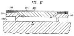
- FIG. 17is a cross-sectional view of a compliant chip assembly including a ground plane in accordance with still further embodiments of the present invention.
- FIGS. 1A-Fillustrate a side view of the process of creating the compliant chip package of the present invention on the face surface of a single die, on the face surfaces of multiple die arranged in a coplanar array or on the face surface of an undiced silicon wafer which may be subsequently diced into individual packaged chips or multi-chip modules.
- FIG. 1Ashows a single semiconductor chip 100 with a contact bearing face surface 120 .
- the contacts 110 on the face surface 120are typically aligned in a peripheral region 112 and further define a central region 115 therein.
- a dielectric passivation layeris deposited or adhered onto the face surface 120 of the chip 100 .
- the passivation layermay simply be the SiO 2 passivation layer (not shown) commonly found on the contact bearing surface of semiconductor chips, or a separate dielectric passivation layer 130 may be used, such as an epoxy resin, a polyimide resin, photo-imagable dielectric, etc.
- the passivation layer 130may be spun onto and built up to a planar sheet-like form on the face surface 120 or a dielectric sheet may be laminated to the face surface 120 using any of a number of electronic grade adhesives commonly known and used by those skilled in the art.
- the passivation layer 130covers the face surface 120 of the chip 100 while leaving the chip contacts 110 exposed so that a bond ribbon may be plated thereon in a later step, as described below. Typically, this will be done by depositing or adhering the passivation layer 130 in a continuous sheet on the face surface 120 of the chip 100 .
- a registering systemsuch as an automatic vision system, is used to locate the contacts 110 .
- the passivation layer 130may be exposed and developed without exposing the area above the contacts 110 , that unexposed area may then be removed.
- Another removal process that can be usedis to use a pulse of directed energy, such as an excimer laser, to selectively remove the passivation layer 130 above the contacts 110 .
- a continuous dielectric sheet already having set contact holesmay be registered and laminated to the chip 100 .
- a compliant layer 140is deposited or laminated onto the exposed surface of the passivation layer 130 .
- the compliant layer 140may be stenciled, screened or transfer molded onto the passivation layer 130 using a curable liquid which, when cured, adheres to the passivation layer 130 .
- the compliant layer 140may be adhered to the exposed surface of the passivation layer 130 in the form of cured compliant pads using the aforementioned electronic grade adhesives.
- the compliant layer 140has a substantially flat top surface 147 , which further typically has a gradual, sloping transition 145 between the face surface 120 of the chip 100 and the top surface 147 .
- This transition 145may follow a line of curvature from the passivation layer 130 to a substantially flat top surface 147 or may simply be canted at an angle such that the transition 145 is not too vertically oriented in relation to the passivation layer 130 and the top surface 147 .
- the compliant layer 140itself may be formed from a wide variety of materials; however, preferably, a low modulus of elasticity material is used as the compliant layer 140 .
- Compliant interposerstypically are fabricated from polymeric and other materials such as silicones, flexibilized epoxy, polyimides and other thermosetting polymers, fluoropolymers and thermoplastic polymers. Also, the interposer may be a composite incorporating plural materials. The interposer may consist of, or incorporate, a foam or mesh layer.
- the flexibility of the interposerdepends on the thickness and configuration of the interposer, as well as on the properties of the materials used therein.
- a flexible interposercapable of buckling or wrinkling to accommodate relative movement, can be fabricated from high elastic modulus materials, normally considered as “rigid” provided that these materials are present in thin layers.
- Relatively soft materials and foamscan be used in greater thicknesses and still provide a highly flexible interposer.
- such soft materials and foamsprovide a highly compliant interposer, i.e., an interposer that is readily compressible in the directions perpendicular its surfaces and which therefore permits movement of the terminals in these directions.
- a plating seed layer 150is then deposited atop the aforementioned assembly, as shown in FIG. 1D , typically using a sputtering operation.
- Typical plating seed layer materialsinclude palladium (for electroless plating), titanium, tungsten, nickel, and chromium; however, primarily copper seed layers are used.
- FIG. 1Eshows the next step in which photoresist 160 is applied to the exposed top surfaces of the assembly and then exposed and developed such that bond ribbons 170 may be plated within defined areas to form conductive paths electrically connecting the chip contacts 110 near a first end region of the ribbons 170 to terminals 175 comprising the second end region of the ribbons 170 . This is perhaps more easily seen in the perspective view shown in FIG. 2 .
- the ribbons 170are plated directly onto the contacts 110 and extend in a “fan-in” arrangement from the peripheral region 112 to the central region 115 of the face surface 120 of the chip 100 atop the compliant layer 140 .
- Possible bond ribbon materialsinclude copper, gold, nickel, and alloys, combinations and composites thereof, among others. Since the bond ribbons 170 are plated directly onto the chip contact/compliant layer themselves, there is no need to develop a process for bonding the ribbons 170 to the contacts, as is necessary with most other approaches such as TAB, beam lead or wirebonding. This provides a significant cost savings because specialized thermocompression or ultrasonic bonders and their bonding tools need not be purchased or maintained.
- the material selected for the bond ribbon 170be compatible with the chip contact 110 material, which is typically aluminum. Otherwise, a phenomenon called Kirkendahl Voiding (voids created at the boundary of two metals having different interdiffusion coefficients) may cause voiding along the boundary of the two metals (ribbon/contact) leading to intermetallic degradation and embrittlement of the bond ribbon 170 itself making the lead/bond susceptible to failure during thermal cycling. Alternately, one or more barrier metals may be plated atop the chip contacts 110 prior to the bond ribbon plating step to thereby ensure the compatibility of materials.
- Kirkendahl Voidingvoids created at the boundary of two metals having different interdiffusion coefficients
- one or more barrier metalsmay be plated atop the chip contacts 110 prior to the bond ribbon plating step to thereby ensure the compatibility of materials.
- a dielectric layer 180is deposited or laminated over the top of the assembly so that only the terminals 175 are exposed.
- the dielectric layermay be comprised of a screened, exposed and developed or laminated sheet photo resist material or may be comprised of paralyne, epoxy resin, polyimide resin, fluoropolymer, etc. which is deposited or laminated on to the assembly, as described above in relation to the passivation layer 130 .
- the terminals 175may then be electrically connected to a circuitized substrate, such as a printed wiring board.
- solder ball or a solid-core solder ballwill be used to create this electrical connection.
- the dielectric layer 180is thus used as a solder mask to ensure that the solder does not electrically short between adjacent bond ribbons 170 .
- Oxide layers and other surface contaminatestypically build up on the surface of many types of metal (copper, nickel, etc.).
- the terminals 175are typically flash plated with a thin layer of gold (approximately 0.25 to 0.5 microns) to inhibit the formation of these oxide layers.
- the gold layeris kept very thin so that it does not appreciably affect the aforementioned solder joint by dissolving into the solder to an amount which would embrittle the resulting solder joint between the terminal and a circuitized substrate.
- the configuration of the above described chip packageallows the package to mechanically decouple the chip 100 from an attached circuitized substrate (not shown). Typically, solder connections between the chip and the circuitized substrate are woefully inadequate to compensate for the thermal mismatch problem during temperature cycling of the chip.
- the combination of the compliant layer 140 and the flexible bond ribbons plated thereonallow the package to compensate for much of the TCE mismatch problem by giving limited movement of the terminals in the X, Y and Z directions with respect to the chip contacts 110 thereby minimizing the stress placed on the solder connections themselves, without imposing substantial forces on the bond between the ribbons 170 and the chip contacts 110 .
- the compliant layer 140is compressible, it also has the effect of compensating for any terminals 175 which are not perfectly planar with respect to its adjacent terminals when the terminals 175 are abutted against and coupled to the circuitized substrate.
- the top surface 147 of the compliant layer 140should be made as flat and planar as possible so that the terminals 175 all lie in or near the same plane in order to minimize the amount of pressure needed to be placed on the bottom surface 125 of the chip 100 to ensure that all of the terminals/solder balls are electrically connected to a circuitized substrate.
- the chip package described above in relation to FIGS. 1 and 2may also be provided in the form of a multiplicity of packages on a wafer incorporating a plurality of individual, undiced chips, all of the same design or of differing designs.
- an array of individual passivation layers 230may be deposited or laminated onto the face surface 220 of the wafer 200 leaving the chip contacts 210 of the various individual chips exposed, as described above. This arrangement is shown to better define the individual chips within the wafer.
- a single passivation layer 230is deposited or laminated onto the face surface 220 leaving the contacts 210 exposed.
- Individual compliant layers 240are deposited or laminated onto the central regions of each of the individual chips within the wafer 200 .
- the steps found in FIG. 1A-Fare then performed, as described above, to create a plurality of connected individually packaged chips on the face surface 220 of the wafer 200 .
- Each packaged chiphaving bond ribbons 270 which are connected at one end to contacts 210 and extending in to a central region of the respective chip in a fan-in fashion atop a respective compliant layer 240 and ending with a terminal 275 on the top surface 247 of the compliant layer 240 .
- the individual chipsmay be separated from the wafer 200 and from one another, as by cutting the wafer 200 using conventional wafer severing or “dicing” equipment commonly utilized to sever wafers into individual chips. This procedure yields a plurality of packaged chip subassemblies, each of which may be secured to an individual circuitized substrate. Alternately, the chips may be separated from the wafer 200 in multi-chip arrangements of multiples of the same or different operational chips.
- the wafer level embodiment shown in FIG. 3could be simulated using a panel of individual chips spaced apart from one another in a processing boat. The face surfaces of the individual chips would be coplanar with respect to one another to simulate the face surface 220 of the wafer 200 .
- the chips above described stepswould be performed and the chips would be separated if desired.
- a low modulus encapsulant material 290may be deposited around the exposed surfaces of the bond ribbons 170 ′ leads prior to the step shown in FIG. 1F of depositing or laminating the assembly with the dielectric layer 180 ′.
- the encapsulant material 290may have properties similar to those of rubber, gum or gel.
- Typical encapsulation materialsinclude curable liquid or cured pads comprised of silicone, flexibilized epoxy, gels, thermoplastics, etc.
- a fixturemay be made such that the liquid flows around the bond ribbons 170 ′ but does not flow on top of the terminals 175 ′ to ensure that solder balls may be subsequently electrically connected to the terminals 175 ′, as described above.
- a machinesuch as a Camalot 1818 manufactured by Camalot Systems, Inc. of Havermill, Mass. may be used to flow the liquid encapsulant into the desired areas. After the liquid is deposited, it may be cured by any number of ways depending on the encapsulant material 290 used, e.g. heat, infrared energy, etc.
- the encapsulant 290gives each of the bond ribbons 170 ′ more support and further spreads some of the stress away from the ribbons 170 ′ thus allowing a larger TCE mismatch between the chip and a circuitized substrate, as described above.
- the dielectric layer 180 ′may be deposited or laminated thereto.
- a conductive materialsuch as beryllium copper, or a super plastic or shape memory alloy (such as Nitinol), is sputtered or otherwise deposited across the entire exposed surface of the chip/passivation layer/compliant layer ( 100 / 130 / 140 ) combination, shown in FIG. 1C .
- the conductive materialmay then be etched using industry standard photolithographic techniques resulting in a multiplicity of bond ribbons positioned and configured much like the bond ribbons 170 shown in FIG. 1E and FIG. 2 .
- a barrier metalsuch as a flash plated layer of gold, may first be plated to the chip contacts to ensure compatibility of the electrical connection between the chip contact and the bond ribbon.
- a flash plated layer of goldmay be plated atop the exposed surface of the terminal.
- the entire exposed surface of the bond ribboncould be plated with a thin layer of gold to increase the overall conductivity of such super plastic leads.
- a dielectric layeris next deposited or laminated as shown in FIG. 1F .
- FIG. 5Ashows a side view and FIG. 5B a perspective view of another embodiment, according to the present invention.
- the compliant layer 140 ′has protrusions 300 on its top surface 147 ′. These protrusions 300 may be integral with the compliant layer 140 ′ or may be deposited or laminated onto the top surface 147 ′ subsequent to the formation of the compliant layer 140 ′.
- the protrusions 300may be formed of compliant, elastomeric material, such as the material comprising the compliant layer 140 ′, or may be comprised of a semi-rigid or rigid material.
- the bond ribbon terminals 175 ′are plated on top of the protrusions 300 thereby providing raised surfaces that may be connected to a circuitized substrate. This technique allows for connection to such a substrate using less solder and without the need to accurately position solid-core solder balls.
- FIG. 6Ashows a side view and FIG. 6B a perspective view of another embodiment, according to the present invention.
- concave areas 310are created in the compliant layer 140 ′′. These concave areas 310 may be create in the formation of the compliant layer 140 ′′ or may be created subsequent to the formation of the compliant layer 140 ′′.
- the bond ribbon terminals 175 ′′are plated within the concave areas 310 creating conductive “cup-like” areas on the top surface 147 ′′ of the compliant layer 140 ′′. Solder or solid-core solder balls are then placed within these areas 310 and reflowed to attach the package to a circuitized substrate, as described earlier. This technique allows for the accurate placement of solder or solid-core solder balls by allowing them to be deposited and retained within the cup-like areas.
- FIGS. 7A-7Dillustrate a side view of a method of making a compliant microelectronic package including a semiconductor chip having an area array of contacts on a first surface thereof.
- the packageis preferably assembled by using the method steps described above.
- FIG. 7Ashows a single semiconductor chip 400 having a first surface 420 including a plurality of contacts 410 provided in an area array over the first surface 400 .
- a dielectric passivation layer 430is deposited over the first surface 420 of the chip 400 and preferably covers the first surface 420 of the chip 400 while leaving the chip contacts 410 exposed so that a bond ribbon (not shown) may be plated thereon, as will be described in more detail below.
- the chip 400including the passivation layer 430 , is placed in a mold 488 so that a compliant layer may be formed atop the passivation layer 430 .
- the compliant layer 440is preferably molded onto the passivation layer 430 using a curable liquid which, when cured, adheres to the passivation layer 430 .
- the mold 488has downwardly extending projections 489 which are shaped to completely cover the chip contacts 410 when the mold 488 is in a closed position.
- the mold 488includes open spaces 493 between the projections 489 .
- the chip 400is placed in a frame 491 and the mold is closed on top of the chip 400 so that the projections 489 completely cover the contacts 410 .
- a curable liquid 440is introduced into the mold and fills the open spaces 493 between the projections 489 .
- the curable liquidis then cured while the mold remains in the closed position so as to form the compliant layer 440 having a substantially flat top surface 447 including a plurality of openings 495 aligned with the contacts 410 .
- the height of projections 489is exaggerated in FIG. 7B for clarity of illustration.
- projections 489typically are about 75-200 microns high, and hence compliant layer 440 typically is about 74-200 microns thick.
- each opening 495has a gradual sloping edge 497 or transition between the first surface 420 of the chip 400 and the top surface 447 of the compliant layer 440 .
- This sloping edge 497will preferably follow a line of curvature from the passivation layer 430 to the substantially flat top surface 447 , or may simply be canted at an angle such that the sloping edge 497 is not too vertically oriented in relation to the passivation layer 430 and the top surface 447 of the compliant layer.
- sloping edge 497typically is disposed at an angle of about 20-70° to the plane of the chip front surface, and more typically about 40-60°.
- the sloping surfacetypically is curved to define a radius at the juncture of sloping surface 497 and top surface 447 .
- a further radius or filletcan be provided at the junction of the sloping surface and the front surface of the chip.
- bond ribbons 470are selectively formed within defined areas to create conductive paths electrically connecting the chip contacts 410 near a first end of the bond ribbons 470 to conductive terminals 475 at a second end of the bond ribbons.
- the bond ribbons 470may be formed using selective electroplating or other selective deposition techniques.
- the selection forming step used to make bond ribbons 470may include one or more non-selective deposition techniques such as electroless plating or sputtering of a conductive layer over the assembly, with or without an additional non-selective electroplating step, followed by selectively etching of the conductive layer to provide electrically isolated bond ribbons.
- FIG. 8Ashows a perspective view of the bond ribbons after they have been selectively formed over the compliant layer.
- one or more barrier metal layersmay be plated atop the chip contacts 410 prior to forming the bond ribbons 470 so as to insure the compatibility of materials.
- a dielectric layer 480is then deposited or laminated over the top of the assembly so that only the conductive terminals 475 are accessible at the top of the assembly.
- the terminals 475may then be electrically interconnected with an external circuit element, such as a printed circuit board.
- an external circuit elementsuch as a printed circuit board.
- a solder ball or solid core solder ballwill be used to create this electrical connection.
- the dielectric layer 480serves as a solder mask, thereby insuring that the solder does not electrically short between adjacent bond ribbons 470 .
- FIG. 8Bshows a close-up, fragmentary, cross-sectional view of FIG. 7D .
- the assemblyincludes the compliant layer 440 having a plurality of apertures 495 therein so the contacts 410 are accessible through the apertures 495 .
- Each aperture 495 in the compliant layer 440preferably includes at least one sloping edge side wall 497 that provides a gradual sloping transition between the first surface 420 of the chip 400 and the top surface 447 of the compliant layer 440 .
- the transitionpreferably follows a line of curvature from the passivation layer 430 to the top surface 447 or may simply be canted at an angle so that the transition from the first surface 420 of the chip 400 to the top surface 447 of the compliant layer 440 is not too vertically oriented in relation to the passivation layer 430 .
- the top surface 447 of the passivation layeris preferably substantially flat, however, in certain embodiments the top surface 447 may be slightly rounded.
- the low points in the compliant layermay next be filled with compliant material to encase the leads and/or cover sheets of material.
- a compliant chip package in accordance with another preferred embodiment of the present inventionincludes a single semiconductor chip 500 having a first surface 520 with a first or central region 515 and a second or peripheral region 517 surrounding the central region 515 .
- the chip 500includes a plurality of contacts 510 disposed in the central region 515 thereof.
- a passivation layer 530is preferably deposited over the first surface 520 of the chip 500 .
- the passivation layer 530includes apertures aligned with the contacts 510 so that the chip contacts 510 are accessible through the passivation layer 530 .
- a compliant layer 540is then formed over the passivation layer, the compliant layer having openings 595 in alignment with the chip contacts 510 so that the contacts are accessible through the compliant layer openings 595 .
- the steps described aboveare then performed to create a plurality of bond ribbons 570 which are connected at one end to the chip contacts 510 and at a second end to conductive terminals 575 accessible at the substantially flat surface 547 of the compliant layer 540 .
- the final assemblyprovides a compliant chip package having a plurality of contacts 510 in the central region 515 thereof and bond ribbons 570 extending outwardly from the contacts 510 to conductive terminals 575 overlying the peripheral region 517 of the chip 500 .
- the centrally located low point in the compliant layercan be filled in with compliant material to encapsulate the leads.
- FIG. 10shows a perspective view of the package illustrated in FIG. 9 .
- the plurality of contacts 510is located in the central region 515 of the chip 500 .
- Compliant layer 540defines two sloping edges 572 at the border of the first or central region of the chip surface and the second or peripheral region.
- Bond ribbons 570have first ends electrically connected to the contacts 510 and second ends extending to conductive terminals 575 provided at the top surface 547 of the compliant layer 540 .
- the specific embodiment shown in FIG. 10includes a compliant layer 540 having a first section on the left side of the chip 500 and a second section on the right side of the chip 500 , however, other preferred embodiments may include compliant layers having more than two distinct portions.
- a compliant chip packageincludes a semiconductor chip 600 having a first surface with a central region 615 and a peripheral region 612 surrounding the central region 615 .
- the peripheral region 612includes a plurality of contacts 610 which are arranged in a staggered or non-uniform configuration.
- the peripheral region 612includes contacts 610 which are positioned at non-uniform distances from an edge 617 of the chip 600 .
- the chipmay include contacts clumped together in groups and/or disposed in a non-uniform pattern throughout the entire first surface of the chip.
- FIG. 12shows four different contacts, designated 610 A- 610 D, located in the peripheral region 612 of the chip 600 .
- the contactsare staggered with respect to one another so that contacts 610 B and 610 D are closer to the edge 617 of the chip than contacts 610 A and 610 C.
- the contacts 610are electrically connected to terminals 675 by bond ribbons 670 .
- the actual length of bond ribbons 670may vary based upon the position of the contact 610 and the desired position of the terminal 675 .
- bond ribbon 670 Cis longer than bond ribbon 670 A.
- the terminal 675 C connected to bond ribbon 670 Cmay be positioned at a more central location than terminal 675 A.
- the ability to modify the length of the bond ribbons 670allows the terminals 675 to be positioned at an infinite number of different locations over the top surface 647 of the compliant layer 640 so that the chip package can be reliably interconnected with an external circuit element, regardless of the location of contact pads on the external circuit element.
- the compliant chip packageincludes a supporting element 792 adjacent a semiconductor chip 700 , with conductive terminals 775 formed over a top surface 794 of the supporting element 792 .
- the supporting element 792may include a bar or alternatively a ring having an opening 795 in the center thereof.
- the semiconductor chip 700is provided within the opening 795 so that a first contact bearing surface 720 of the chip 700 is substantially parallel with the top surface 794 of the supporting element 792 .
- the first surface 720 of the semiconductor chip 700preferably includes a passivation layer 730 having openings therein so that the contacts 710 are accessible through the openings.
- a compliant layer 740 having a substantially flat top surface 747 and a bottom surface and sloping edges 797 therebetweenis then formed atop the top surface 794 of the supporting element 792 and a portion of the passivation layer 730 .
- the compliant layer 740preferably fills gaps 755 between the peripheral edges of the chip 700 and the support element 792 .
- the compliant layer 740preferably has a meniscus-shaped top surface so that the transition from the passivation layer 730 to the compliant layer 740 is smooth. This smooth transition will increase the reliability of any bond ribbons formed atop the compliant layer because the bond ribbons will be gently curved rather than kinked.
- bond ribbons 770are formed using the techniques described above, and a dielectric layer 780 is formed over the bond ribbons 770 so that only conductive terminals 775 are accessible at the top of the assembly.
- the supporting element 792may include a heat sink and the compliant layer may be formed on the top surface of flanges extending laterally from central opening in the heat sink.
- the compliant chip packageincludes a flexible dielectric sheet 865 , such as a polyimide sheet, secured over the top of the compliant layer 840 .
- the packageincludes a semiconductor chip 800 having a first surface 820 with contacts 810 .
- a dielectric passivation layer 830including openings in substantial alignment with the contacts 810 , is then formed over the first surface 820 of the chip 800 .
- the flexible dielectric sheet 865is provided over the top surface 847 of the compliant layer 840 .
- the flexible dielectric sheet 865generally improves the structural integrity of the package and protects the compliant layer 840 from external contaminants.
- Bond ribbons 870are then formed atop the passivation layer 830 , the compliant layer 840 and the flexible dielectric sheet 865 .
- the bonds ribbons 870have first ends which are connected to chip contacts 810 and second ends which provide conductive terminals 875 over the flexible dielectric sheet 865 .
- the dielectric sheet 865is provided as a separate sheet which is laminated or secured over the top surface 847 of the compliant layer 840 .
- the conductive terminals 875may be pre-formed on the dielectric sheet 865 , with the bond ribbon forming step electrically interconnecting the contacts 810 and the pre-formed conductive terminals 875 .
- the flexible dielectric sheet 865may be spun onto the top surface 847 of the compliant layer 840 .
- the edges of the spun-on dielectric sheethave radii of curvature which substantially match the radii of curvature of the edges of the compliant layer.
- the matched edgesprovide a smooth transition from the dielectric sheet 865 to the compliant layer 840 , thereby providing a more uniform surface for forming the bond ribbons 870 .
- a second dielectric protective layer 880may then be formed over the bond ribbons 870 to further protect the bond ribbons and electrically isolate the bond ribbons from one another.
- a compliant chip packagein another embodiment, illustrated in FIGS. 15 and 16 , includes a ground plane 981 .
- a semiconductor chip 900is provided within a central opening 995 of a supporting element 992 so that a first contact bearing surface 920 of the chip 900 is substantially parallel with a top surface 994 of the supporting element 992 .
- a first compliant layer 940having a substantially flat top surface 947 and a bottom surface and sloping edges 997 therebetween is then formed atop the top surface 994 of the supporting element 992 .
- the compliant layer 940preferably fills gaps 955 between the peripheral edges of the chip 900 and the support element 992 .
- the sloping edges 997preferably provide a smooth transition between the top surface 947 of the compliant layer 940 and the chip 900 .
- Bond ribbonsare then formed over the compliant layer 940 using the techniques described above.
- the sloping edges 997 of the compliant layer 940will increase the reliability of the bond ribbons 970 because the bond ribbons will be gently curved rather than kinked.
- a second compliant layer 941is formed atop the bond ribbons 970 so as to encapsulate the bond ribbons 970 .
- a dielectric layer 980is then formed over the second compliant layer 941 and the bond ribbons 970 so that only conductive terminals 975 are accessible at the top of the assembly.
- the ground plane 981is then provided atop the dielectric layer 980 .
- the ground planepreferably includes a highly conductive material, such as copper, having a plurality of openings therein.
- the openingsare preferably formed using photolithographic and etching techniques.
- the openingsare sized to fit over the terminals 975 and a relatively small portion of the bond ribbon 970 extending away from each terminal 975 .
- the ground plane 981is assembled to the dielectric layer by aligning the openings 983 therein with the terminals 975 and abutting the ground plane 981 against the top of the dielectric layer 980 .
- the packageis then subjected to a curing process so as to cure the compliant layers 940 and 941 and the dielectric layer 980 .
- FIG. 17shows yet another embodiment of a compliant chip package which is similar to that shown in FIG. 15 , however, the FIG. 17 embodiment lacks the top dielectric cover layer shown in FIG. 15 .
- a ground plane 1081similar to that shown in FIG. 16 is provided over the second compliant layer 1041 .
- the ground plane 1081may be compressed against the second compliant layer 1041 so that the ground plane 1081 is slightly sunk into the second compliant layer 1041 .
- the ground planepreferably includes openings 1083 which are in alignment with terminals 1075 so that the terminals 1075 are accessible through the openings 1083 .
- the packageis then subjected to a curing process so as to cure the compliant layers 1040 and 1041 .
- the ground plane 1081is preferably electrically connected to at least one of the bond ribbons 1070 .
- the low modulus encapsulant material shown in FIG. 4may be used to assemble any of the compliant chip packages shown in FIGS. 7A-14 to provide additional stress relief for the bond ribbons.
- the assembly shown in FIG. 13may be modified so as to provide conductive terminals over the central region of the chip, thereby providing a “fan-in/fan-out” compliant chip package.
- all of the chip package assemblies disclosed abovemay be assembled on a wafer prior to severing the individual chips from the wafer.
Landscapes
- Engineering & Computer Science (AREA)
- Microelectronics & Electronic Packaging (AREA)
- Computer Hardware Design (AREA)
- Power Engineering (AREA)
- Physics & Mathematics (AREA)
- Condensed Matter Physics & Semiconductors (AREA)
- General Physics & Mathematics (AREA)
- Manufacturing & Machinery (AREA)
- Internal Circuitry In Semiconductor Integrated Circuit Devices (AREA)
- Wire Bonding (AREA)
Abstract
Description
Claims (21)
Priority Applications (3)
| Application Number | Priority Date | Filing Date | Title |
|---|---|---|---|
| US11/474,199US7872344B2 (en) | 1995-10-31 | 2006-06-23 | Microelectronic assemblies having compliant layers |
| US11/487,263US7408260B2 (en) | 1995-10-31 | 2006-07-14 | Microelectronic assemblies having compliant layers |
| US12/974,744US8338925B2 (en) | 1995-10-31 | 2010-12-21 | Microelectronic assemblies having compliant layers |
Applications Claiming Priority (8)
| Application Number | Priority Date | Filing Date | Title |
|---|---|---|---|
| US712895P | 1995-10-31 | 1995-10-31 | |
| US08/739,303US6211572B1 (en) | 1995-10-31 | 1996-10-29 | Semiconductor chip package with fan-in leads |
| US09/071,412US6284563B1 (en) | 1995-10-31 | 1998-05-01 | Method of making compliant microelectronic assemblies |
| US09/777,782US6465878B2 (en) | 1995-10-31 | 2001-02-06 | Compliant microelectronic assemblies |
| US10/107,094US6847101B2 (en) | 1995-10-31 | 2002-03-26 | Microelectronic package having a compliant layer with bumped protrusions |
| US10/219,902US6847107B2 (en) | 1995-10-31 | 2002-08-15 | Image forming apparatus with improved transfer efficiency |
| US10/873,883US7112879B2 (en) | 1995-10-31 | 2004-06-22 | Microelectronic assemblies having compliant layers |
| US11/474,199US7872344B2 (en) | 1995-10-31 | 2006-06-23 | Microelectronic assemblies having compliant layers |
Related Parent Applications (1)
| Application Number | Title | Priority Date | Filing Date |
|---|---|---|---|
| US10/873,883ContinuationUS7112879B2 (en) | 1995-10-31 | 2004-06-22 | Microelectronic assemblies having compliant layers |
Related Child Applications (2)
| Application Number | Title | Priority Date | Filing Date |
|---|---|---|---|
| US11/487,263ContinuationUS7408260B2 (en) | 1995-10-31 | 2006-07-14 | Microelectronic assemblies having compliant layers |
| US12/974,744ContinuationUS8338925B2 (en) | 1995-10-31 | 2010-12-21 | Microelectronic assemblies having compliant layers |
Publications (2)
| Publication Number | Publication Date |
|---|---|
| US20060237836A1 US20060237836A1 (en) | 2006-10-26 |
| US7872344B2true US7872344B2 (en) | 2011-01-18 |
Family
ID=27358284
Family Applications (8)
| Application Number | Title | Priority Date | Filing Date |
|---|---|---|---|
| US09/071,412Expired - LifetimeUS6284563B1 (en) | 1995-10-31 | 1998-05-01 | Method of making compliant microelectronic assemblies |
| US09/777,782Expired - LifetimeUS6465878B2 (en) | 1995-10-31 | 2001-02-06 | Compliant microelectronic assemblies |
| US10/107,094Expired - LifetimeUS6847101B2 (en) | 1995-10-31 | 2002-03-26 | Microelectronic package having a compliant layer with bumped protrusions |
| US10/219,902Expired - LifetimeUS6847107B2 (en) | 1995-10-31 | 2002-08-15 | Image forming apparatus with improved transfer efficiency |
| US10/873,883Expired - Fee RelatedUS7112879B2 (en) | 1995-10-31 | 2004-06-22 | Microelectronic assemblies having compliant layers |
| US11/474,199Expired - Fee RelatedUS7872344B2 (en) | 1995-10-31 | 2006-06-23 | Microelectronic assemblies having compliant layers |
| US11/487,263Expired - Fee RelatedUS7408260B2 (en) | 1995-10-31 | 2006-07-14 | Microelectronic assemblies having compliant layers |
| US12/974,744Expired - Fee RelatedUS8338925B2 (en) | 1995-10-31 | 2010-12-21 | Microelectronic assemblies having compliant layers |
Family Applications Before (5)
| Application Number | Title | Priority Date | Filing Date |
|---|---|---|---|
| US09/071,412Expired - LifetimeUS6284563B1 (en) | 1995-10-31 | 1998-05-01 | Method of making compliant microelectronic assemblies |
| US09/777,782Expired - LifetimeUS6465878B2 (en) | 1995-10-31 | 2001-02-06 | Compliant microelectronic assemblies |
| US10/107,094Expired - LifetimeUS6847101B2 (en) | 1995-10-31 | 2002-03-26 | Microelectronic package having a compliant layer with bumped protrusions |
| US10/219,902Expired - LifetimeUS6847107B2 (en) | 1995-10-31 | 2002-08-15 | Image forming apparatus with improved transfer efficiency |
| US10/873,883Expired - Fee RelatedUS7112879B2 (en) | 1995-10-31 | 2004-06-22 | Microelectronic assemblies having compliant layers |
Family Applications After (2)
| Application Number | Title | Priority Date | Filing Date |
|---|---|---|---|
| US11/487,263Expired - Fee RelatedUS7408260B2 (en) | 1995-10-31 | 2006-07-14 | Microelectronic assemblies having compliant layers |
| US12/974,744Expired - Fee RelatedUS8338925B2 (en) | 1995-10-31 | 2010-12-21 | Microelectronic assemblies having compliant layers |
Country Status (1)
| Country | Link |
|---|---|
| US (8) | US6284563B1 (en) |
Cited By (30)
| Publication number | Priority date | Publication date | Assignee | Title |
|---|---|---|---|---|
| US20110242708A1 (en)* | 2010-03-31 | 2011-10-06 | Nhk Spring Co., Ltd. | Electronic apparatus and disk drive suspension |
| US20130099359A1 (en)* | 2011-10-21 | 2013-04-25 | SK Hynix Inc. | Semiconductor package and stacked semiconductor package |
| US20130228897A1 (en)* | 2012-03-01 | 2013-09-05 | Taiwan Semiconductor Manufacturing Company, Ltd. | Electrical Connections for Chip Scale Packaging |
| US20130302941A1 (en)* | 2007-03-09 | 2013-11-14 | Micron Technology, Inc. | Microelectronic workpieces and methods for manufacturing microelectronic devices using such workpieces |
| US8885299B1 (en) | 2010-05-24 | 2014-11-11 | Hutchinson Technology Incorporated | Low resistance ground joints for dual stage actuation disk drive suspensions |
| US8891206B2 (en) | 2012-12-17 | 2014-11-18 | Hutchinson Technology Incorporated | Co-located gimbal-based dual stage actuation disk drive suspensions with motor stiffener |
| US8896970B1 (en) | 2013-12-31 | 2014-11-25 | Hutchinson Technology Incorporated | Balanced co-located gimbal-based dual stage actuation disk drive suspensions |
| US8896968B2 (en) | 2012-10-10 | 2014-11-25 | Hutchinson Technology Incorporated | Co-located gimbal-based dual stage actuation disk drive suspensions with dampers |
| US8896969B1 (en) | 2013-05-23 | 2014-11-25 | Hutchinson Technology Incorporated | Two-motor co-located gimbal-based dual stage actuation disk drive suspensions with motor stiffeners |
| US8941951B2 (en) | 2012-11-28 | 2015-01-27 | Hutchinson Technology Incorporated | Head suspension flexure with integrated strain sensor and sputtered traces |
| US9001469B2 (en) | 2012-03-16 | 2015-04-07 | Hutchinson Technology Incorporated | Mid-loadbeam dual stage actuated (DSA) disk drive head suspension |
| US9001471B2 (en) | 2012-09-14 | 2015-04-07 | Hutchinson Technology Incorporated | Co-located gimbal-based dual stage actuation disk drive suspensions |
| US9007726B2 (en) | 2013-07-15 | 2015-04-14 | Hutchinson Technology Incorporated | Disk drive suspension assembly having a partially flangeless load point dimple |
| US20150194347A1 (en)* | 1995-10-31 | 2015-07-09 | Tessera, Inc. | Methods of making compliant semiconductor chip packages |
| US9087882B2 (en) | 2011-06-03 | 2015-07-21 | Taiwan Semiconductor Manufacturing Company, Ltd. | Electrical connection for chip scale packaging |
| US9093117B2 (en) | 2012-03-22 | 2015-07-28 | Hutchinson Technology Incorporated | Ground feature for disk drive head suspension flexures |
| US9099131B1 (en) | 2010-03-17 | 2015-08-04 | Western Digital Technologies, Inc. | Suspension assembly having a microactuator electrically connected to a gold coating on a stainless steel surface |
| US9123788B2 (en) | 2012-08-17 | 2015-09-01 | Taiwan Semiconductor Manufacturing Company, Ltd. | Bonded structures for package and substrate |
| US9230580B1 (en) | 2010-06-30 | 2016-01-05 | Western Digital Technologies, Inc. | Suspension assembly having a microactuator grounded to a flexure |
| US9296188B1 (en) | 2015-02-17 | 2016-03-29 | Hutchinson Technology Incorporated | Partial curing of a microactuator mounting adhesive in a disk drive suspension |
| US9431042B2 (en) | 2014-01-03 | 2016-08-30 | Hutchinson Technology Incorporated | Balanced multi-trace transmission in a hard disk drive flexure |
| US9548281B2 (en) | 2011-10-07 | 2017-01-17 | Taiwan Semiconductor Manufacturing Company, Ltd. | Electrical connection for chip scale packaging |
| US9558771B2 (en) | 2014-12-16 | 2017-01-31 | Hutchinson Technology Incorporated | Piezoelectric disk drive suspension motors having plated stiffeners |
| US9564154B2 (en) | 2014-12-22 | 2017-02-07 | Hutchinson Technology Incorporated | Multilayer disk drive motors having out-of-plane bending |
| US9570373B1 (en) | 2015-12-09 | 2017-02-14 | International Business Machines Corporation | Near-chip compliant layer for reducing perimeter stress during assembly process |
| US9646638B1 (en) | 2016-05-12 | 2017-05-09 | Hutchinson Technology Incorporated | Co-located gimbal-based DSA disk drive suspension with traces routed around slider pad |
| US9673161B2 (en) | 2012-08-17 | 2017-06-06 | Taiwan Semiconductor Manufacturing Company, Ltd. | Bonded structures for package and substrate |
| US9734852B2 (en) | 2015-06-30 | 2017-08-15 | Hutchinson Technology Incorporated | Disk drive head suspension structures having improved gold-dielectric joint reliability |
| US9748188B2 (en) | 2012-07-31 | 2017-08-29 | Taiwan Semiconductor Manufacturing Company, Ltd. | Method of forming a bump on pad (BOP) bonding structure in a semiconductor packaged device |
| US10978313B2 (en) | 2018-02-20 | 2021-04-13 | International Business Machines Corporation | Fixture facilitating heat sink fabrication |
Families Citing this family (145)
| Publication number | Priority date | Publication date | Assignee | Title |
|---|---|---|---|---|
| US6870272B2 (en) | 1994-09-20 | 2005-03-22 | Tessera, Inc. | Methods of making microelectronic assemblies including compliant interfaces |
| US6284563B1 (en) | 1995-10-31 | 2001-09-04 | Tessera, Inc. | Method of making compliant microelectronic assemblies |
| SG73490A1 (en) | 1998-01-23 | 2000-06-20 | Texas Instr Singapore Pte Ltd | High density internal ball grid array integrated circuit package |
| US8021976B2 (en) | 2002-10-15 | 2011-09-20 | Megica Corporation | Method of wire bonding over active area of a semiconductor circuit |
| US6940160B1 (en)* | 1999-03-16 | 2005-09-06 | Seiko Epson Corporation | Semiconductor device and method of manufacture thereof, circuit board, and electronic instrument |
| WO2000077844A1 (en)* | 1999-06-15 | 2000-12-21 | Fujikura Ltd. | Semiconductor package, semiconductor device, electronic device, and method of manufacturing semiconductor package |
| KR20020011440A (en)* | 1999-06-17 | 2002-02-08 | 마이클 골위저, 호레스트 쉐퍼 | Electronic component with flexible contact structures and method for the production of said component |
| US6228687B1 (en)* | 1999-06-28 | 2001-05-08 | Micron Technology, Inc. | Wafer-level package and methods of fabricating |
| US7019410B1 (en)* | 1999-12-21 | 2006-03-28 | Micron Technology, Inc. | Die attach material for TBGA or flexible circuitry |
| US7283059B2 (en)* | 2000-03-15 | 2007-10-16 | Logitech Europe S.A. | Remote control multimedia content listing system |
| US6784805B2 (en) | 2000-03-15 | 2004-08-31 | Intrigue Technologies Inc. | State-based remote control system |
| US8531276B2 (en)* | 2000-03-15 | 2013-09-10 | Logitech Europe S.A. | State-based remote control system |
| US20010033243A1 (en) | 2000-03-15 | 2001-10-25 | Harris Glen Mclean | Online remote control configuration system |
| JP4441974B2 (en)* | 2000-03-24 | 2010-03-31 | ソニー株式会社 | Manufacturing method of semiconductor device |
| DE10016132A1 (en)* | 2000-03-31 | 2001-10-18 | Infineon Technologies Ag | Electronic component with flexible contact points and method for its production |
| US7247932B1 (en) | 2000-05-19 | 2007-07-24 | Megica Corporation | Chip package with capacitor |
| JP3596864B2 (en)* | 2000-05-25 | 2004-12-02 | シャープ株式会社 | Semiconductor device |
| US6875640B1 (en)* | 2000-06-08 | 2005-04-05 | Micron Technology, Inc. | Stereolithographic methods for forming a protective layer on a semiconductor device substrate and substrates including protective layers so formed |
| US6459150B1 (en)* | 2000-08-17 | 2002-10-01 | Industrial Technology Research Institute | Electronic substrate having an aperture position through a substrate, conductive pads, and an insulating layer |
| US6580165B1 (en)* | 2000-11-16 | 2003-06-17 | Fairchild Semiconductor Corporation | Flip chip with solder pre-plated leadframe including locating holes |
| US6617674B2 (en) | 2001-02-20 | 2003-09-09 | Dow Corning Corporation | Semiconductor package and method of preparing same |
| US7498196B2 (en) | 2001-03-30 | 2009-03-03 | Megica Corporation | Structure and manufacturing method of chip scale package |
| DE10116069C2 (en)* | 2001-04-02 | 2003-02-20 | Infineon Technologies Ag | Electronic component with a semiconductor chip and method for its production |
| SG120858A1 (en)* | 2001-08-06 | 2006-04-26 | Micron Technology Inc | Quad flat no-lead (qfn) grid array package, methodof making and memory module and computer system including same |
| DE10143790B4 (en)* | 2001-09-06 | 2007-08-02 | Infineon Technologies Ag | Electronic component with at least one semiconductor chip |
| US6613606B1 (en) | 2001-09-17 | 2003-09-02 | Magic Corporation | Structure of high performance combo chip and processing method |
| SG102639A1 (en)* | 2001-10-08 | 2004-03-26 | Micron Technology Inc | Apparatus and method for packing circuits |
| US7317091B2 (en)* | 2002-03-01 | 2008-01-08 | Xencor, Inc. | Optimized Fc variants |
| US7423336B2 (en)* | 2002-04-08 | 2008-09-09 | Micron Technology, Inc. | Bond pad rerouting element, rerouted semiconductor devices including the rerouting element, and assemblies including the rerouted semiconductor devices |
| US6940177B2 (en)* | 2002-05-16 | 2005-09-06 | Dow Corning Corporation | Semiconductor package and method of preparing same |
| US7265045B2 (en) | 2002-10-24 | 2007-09-04 | Megica Corporation | Method for fabricating thermal compliant semiconductor chip wiring structure for chip scale packaging |
| JP3969295B2 (en) | 2002-12-02 | 2007-09-05 | セイコーエプソン株式会社 | SEMICONDUCTOR DEVICE, ITS MANUFACTURING METHOD, CIRCUIT BOARD, ELECTRO-OPTICAL DEVICE, AND ELECTRONIC DEVICE |
| DE10258094B4 (en)* | 2002-12-11 | 2009-06-18 | Qimonda Ag | Method of forming 3-D structures on wafers |
| US7230339B2 (en)* | 2003-03-28 | 2007-06-12 | Intel Corporation | Copper ring solder mask defined ball grid array pad |
| US7114961B2 (en)* | 2003-04-11 | 2006-10-03 | Neoconix, Inc. | Electrical connector on a flexible carrier |
| US20100167561A1 (en)* | 2003-04-11 | 2010-07-01 | Neoconix, Inc. | Structure and process for a contact grid array formed in a circuitized substrate |
| US8584353B2 (en)* | 2003-04-11 | 2013-11-19 | Neoconix, Inc. | Method for fabricating a contact grid array |
| US7758351B2 (en)* | 2003-04-11 | 2010-07-20 | Neoconix, Inc. | Method and system for batch manufacturing of spring elements |
| US20050120553A1 (en)* | 2003-12-08 | 2005-06-09 | Brown Dirk D. | Method for forming MEMS grid array connector |
| US7113408B2 (en)* | 2003-06-11 | 2006-09-26 | Neoconix, Inc. | Contact grid array formed on a printed circuit board |
| US7628617B2 (en)* | 2003-06-11 | 2009-12-08 | Neoconix, Inc. | Structure and process for a contact grid array formed in a circuitized substrate |
| US7597561B2 (en)* | 2003-04-11 | 2009-10-06 | Neoconix, Inc. | Method and system for batch forming spring elements in three dimensions |
| US20070020960A1 (en)* | 2003-04-11 | 2007-01-25 | Williams John D | Contact grid array system |
| US7244125B2 (en)* | 2003-12-08 | 2007-07-17 | Neoconix, Inc. | Connector for making electrical contact at semiconductor scales |
| US7056131B1 (en) | 2003-04-11 | 2006-06-06 | Neoconix, Inc. | Contact grid array system |
| US20040217488A1 (en) | 2003-05-02 | 2004-11-04 | Luechinger Christoph B. | Ribbon bonding |
| DE10324450A1 (en)* | 2003-05-28 | 2005-01-05 | Infineon Technologies Ag | Contacting device for electronic circuit units and manufacturing method |
| JP3906921B2 (en)* | 2003-06-13 | 2007-04-18 | セイコーエプソン株式会社 | Bump structure and manufacturing method thereof |
| JP4393303B2 (en)* | 2003-09-05 | 2010-01-06 | キヤノン株式会社 | Manufacturing method of semiconductor device |
| US20050093170A1 (en)* | 2003-10-29 | 2005-05-05 | Texas Instruments Incorporated | Integrated interconnect package |
| US20050227510A1 (en)* | 2004-04-09 | 2005-10-13 | Brown Dirk D | Small array contact with precision working range |
| US7294929B2 (en)* | 2003-12-30 | 2007-11-13 | Texas Instruments Incorporated | Solder ball pad structure |
| GB0402960D0 (en)* | 2004-02-10 | 2004-03-17 | Plastic Logic Ltd | Thermal imaging of catalyst in electroless deposition of metal films |
| DE102004009296B4 (en)* | 2004-02-26 | 2011-01-27 | Siemens Ag | Method for producing an arrangement of an electrical component |
| US7090503B2 (en)* | 2004-03-19 | 2006-08-15 | Neoconix, Inc. | Interposer with compliant pins |
| US20050205988A1 (en)* | 2004-03-19 | 2005-09-22 | Epic Technology Inc. | Die package with higher useable die contact pad area |
| WO2005091998A2 (en)* | 2004-03-19 | 2005-10-06 | Neoconix, Inc. | Electrical connector in a flexible host |
| US7025601B2 (en)* | 2004-03-19 | 2006-04-11 | Neoconix, Inc. | Interposer and method for making same |
| US7347698B2 (en)* | 2004-03-19 | 2008-03-25 | Neoconix, Inc. | Deep drawn electrical contacts and method for making |
| KR100632472B1 (en)* | 2004-04-14 | 2006-10-09 | 삼성전자주식회사 | Microelectronic device chip having a fine pitch bump structure having non-conductive sidewalls, a package thereof, a liquid crystal display device comprising the same, and a manufacturing method thereof |
| CN100527398C (en)* | 2004-04-14 | 2009-08-12 | 三星电子株式会社 | Bump structure for a semiconductor device and method of manufacture |
| US7259468B2 (en)* | 2004-04-30 | 2007-08-21 | Advanced Chip Engineering Technology Inc. | Structure of package |
| US20060000642A1 (en)* | 2004-07-01 | 2006-01-05 | Epic Technology Inc. | Interposer with compliant pins |
| US7354276B2 (en)* | 2004-07-20 | 2008-04-08 | Neoconix, Inc. | Interposer with compliant pins |
| CN100385657C (en)* | 2004-09-09 | 2008-04-30 | 精工爱普生株式会社 | Electronic device and manufacturing method thereof |
| US7190157B2 (en)* | 2004-10-25 | 2007-03-13 | Agilent Technologies, Inc. | Method and apparatus for layout independent test point placement on a printed circuit board |
| US7208820B2 (en)* | 2004-12-29 | 2007-04-24 | Tessera, Inc. | Substrate having a plurality of I/O routing arrangements for a microelectronic device |
| US20060138599A1 (en)* | 2004-12-29 | 2006-06-29 | Tessera, Inc. | Semiconductor members having a halogenated polymeric coating and methods for their formation |
| CN101128931B (en)* | 2005-02-25 | 2010-05-19 | 德塞拉股份有限公司 | Microelectronic assemblies having compliancy |
| DE102006018238A1 (en)* | 2005-04-20 | 2007-03-29 | Logitech Europe S.A. | Remote control system for home theater system, analyzes log of events stored by remote controller to identify patterns of interest in logged use of remote controller |
| TW200702762A (en)* | 2005-06-01 | 2007-01-16 | Rohm & Haas Elect Mat | Optical assemblies |
| US20060284313A1 (en)* | 2005-06-15 | 2006-12-21 | Yongqian Wang | Low stress chip attachment with shape memory materials |
| JP4145902B2 (en)* | 2005-07-19 | 2008-09-03 | セイコーエプソン株式会社 | Semiconductor device and manufacturing method thereof |
| JP4273347B2 (en)* | 2005-08-03 | 2009-06-03 | セイコーエプソン株式会社 | Semiconductor device |
| US20070050738A1 (en)* | 2005-08-31 | 2007-03-01 | Dittmann Larry E | Customer designed interposer |
| US8553364B1 (en) | 2005-09-09 | 2013-10-08 | Magnecomp Corporation | Low impedance, high bandwidth disk drive suspension circuit |
| US7829793B2 (en)* | 2005-09-09 | 2010-11-09 | Magnecomp Corporation | Additive disk drive suspension manufacturing using tie layers for vias and product thereof |
| DE102005043657B4 (en)* | 2005-09-13 | 2011-12-15 | Infineon Technologies Ag | Chip module, method for encapsulating a chip and using an encapsulation material |
| JP4305667B2 (en)* | 2005-11-07 | 2009-07-29 | セイコーエプソン株式会社 | Semiconductor device |
| US7357644B2 (en)* | 2005-12-12 | 2008-04-15 | Neoconix, Inc. | Connector having staggered contact architecture for enhanced working range |
| US7534652B2 (en)* | 2005-12-27 | 2009-05-19 | Tessera, Inc. | Microelectronic elements with compliant terminal mountings and methods for making the same |
| KR100713928B1 (en)* | 2006-02-08 | 2007-05-07 | 주식회사 하이닉스반도체 | Semiconductor chip package |
| US20070233731A1 (en)* | 2006-02-22 | 2007-10-04 | Logitech Europe S.A. | System and method for configuring media systems |
| US20070267730A1 (en)* | 2006-05-16 | 2007-11-22 | Tessera, Inc. | Wafer level semiconductor chip packages and methods of making the same |
| TWI317164B (en)* | 2006-07-28 | 2009-11-11 | Taiwan Tft Lcd Ass | Contact structure having a compliant bump and a testing area and manufacturing method for the same |
| US7545029B2 (en) | 2006-08-18 | 2009-06-09 | Tessera, Inc. | Stack microelectronic assemblies |
| US7582966B2 (en) | 2006-09-06 | 2009-09-01 | Megica Corporation | Semiconductor chip and method for fabricating the same |
| US8133808B2 (en)* | 2006-09-18 | 2012-03-13 | Tessera, Inc. | Wafer level chip package and a method of fabricating thereof |
| US20080123335A1 (en)* | 2006-11-08 | 2008-05-29 | Jong Kun Yoo | Printed circuit board assembly and display having the same |
| US7791199B2 (en)* | 2006-11-22 | 2010-09-07 | Tessera, Inc. | Packaged semiconductor chips |
| US8569876B2 (en) | 2006-11-22 | 2013-10-29 | Tessera, Inc. | Packaged semiconductor chips with array |
| JP4956173B2 (en)* | 2006-12-19 | 2012-06-20 | 新光電気工業株式会社 | Flip chip mounting board |
| US7749886B2 (en) | 2006-12-20 | 2010-07-06 | Tessera, Inc. | Microelectronic assemblies having compliancy and methods therefor |
| JP2008198916A (en)* | 2007-02-15 | 2008-08-28 | Spansion Llc | Semiconductor device and manufacturing method thereof |
| US8405196B2 (en)* | 2007-03-05 | 2013-03-26 | DigitalOptics Corporation Europe Limited | Chips having rear contacts connected by through vias to front contacts |
| US7994622B2 (en)* | 2007-04-16 | 2011-08-09 | Tessera, Inc. | Microelectronic packages having cavities for receiving microelectric elements |
| TWI356481B (en)* | 2007-05-18 | 2012-01-11 | Taiwan Tft Lcd Ass | Bump structure |
| US8208266B2 (en) | 2007-05-29 | 2012-06-26 | Avx Corporation | Shaped integrated passives |
| US7691682B2 (en) | 2007-06-26 | 2010-04-06 | Micron Technology, Inc. | Build-up-package for integrated circuit devices, and methods of making same |
| US8193092B2 (en) | 2007-07-31 | 2012-06-05 | Micron Technology, Inc. | Semiconductor devices including a through-substrate conductive member with an exposed end and methods of manufacturing such semiconductor devices |
| WO2009017835A2 (en) | 2007-07-31 | 2009-02-05 | Tessera, Inc. | Semiconductor packaging process using through silicon vias |
| TWI381464B (en)* | 2008-08-29 | 2013-01-01 | Hannstar Display Corp | The bump structure and its making method |
| US7960845B2 (en)* | 2008-01-03 | 2011-06-14 | Linear Technology Corporation | Flexible contactless wire bonding structure and methodology for semiconductor device |
| US20090212381A1 (en)* | 2008-02-26 | 2009-08-27 | Tessera, Inc. | Wafer level packages for rear-face illuminated solid state image sensors |
| US20100053407A1 (en)* | 2008-02-26 | 2010-03-04 | Tessera, Inc. | Wafer level compliant packages for rear-face illuminated solid state image sensors |
| JP4535295B2 (en)* | 2008-03-03 | 2010-09-01 | セイコーエプソン株式会社 | Semiconductor module and manufacturing method thereof |
| TWI377632B (en)* | 2008-03-27 | 2012-11-21 | Taiwan Tft Lcd Ass | Contact structure and forming method thereof and connecting structure thereof |
| CA2726151C (en)* | 2008-05-30 | 2016-11-22 | Koninklijke Philips Electronics N.V. | Round illumination device |
| US7902665B2 (en)* | 2008-09-02 | 2011-03-08 | Linear Technology Corporation | Semiconductor device having a suspended isolating interconnect |
| GB2464549B (en)* | 2008-10-22 | 2013-03-27 | Cambridge Silicon Radio Ltd | Improved wafer level chip scale packaging |
| US20110067910A1 (en)* | 2009-09-18 | 2011-03-24 | International Business Machines Corporation | Component securing system and associated method |
| JP5386302B2 (en)* | 2009-10-27 | 2014-01-15 | ルネサスエレクトロニクス株式会社 | Semiconductor device and manufacturing method of semiconductor device |
| JP5400597B2 (en)* | 2009-12-15 | 2014-01-29 | ルネサスエレクトロニクス株式会社 | Semiconductor device and electronic device |
| US9640437B2 (en) | 2010-07-23 | 2017-05-02 | Tessera, Inc. | Methods of forming semiconductor elements using micro-abrasive particle stream |
| US8796135B2 (en) | 2010-07-23 | 2014-08-05 | Tessera, Inc. | Microelectronic elements with rear contacts connected with via first or via middle structures |
| US8791575B2 (en) | 2010-07-23 | 2014-07-29 | Tessera, Inc. | Microelectronic elements having metallic pads overlying vias |
| US8508401B1 (en) | 2010-08-31 | 2013-08-13 | Logitech Europe S.A. | Delay fixing for command codes in a remote control system |
| US8847380B2 (en) | 2010-09-17 | 2014-09-30 | Tessera, Inc. | Staged via formation from both sides of chip |
| US8610259B2 (en) | 2010-09-17 | 2013-12-17 | Tessera, Inc. | Multi-function and shielded 3D interconnects |
| US8587126B2 (en) | 2010-12-02 | 2013-11-19 | Tessera, Inc. | Stacked microelectronic assembly with TSVs formed in stages with plural active chips |
| US8736066B2 (en) | 2010-12-02 | 2014-05-27 | Tessera, Inc. | Stacked microelectronic assemby with TSVS formed in stages and carrier above chip |
| US8637968B2 (en) | 2010-12-02 | 2014-01-28 | Tessera, Inc. | Stacked microelectronic assembly having interposer connecting active chips |
| US8610264B2 (en) | 2010-12-08 | 2013-12-17 | Tessera, Inc. | Compliant interconnects in wafers |
| US8569167B2 (en)* | 2011-03-29 | 2013-10-29 | Micron Technology, Inc. | Methods for forming a semiconductor structure |
| US8918544B2 (en) | 2011-03-31 | 2014-12-23 | Logitech Europe S.A. | Apparatus and method for configuration and operation of a remote-control system |
| US9239837B2 (en) | 2011-04-29 | 2016-01-19 | Logitech Europe S.A. | Remote control system for connected devices |
| US20120282437A1 (en)* | 2011-05-04 | 2012-11-08 | Saint-Gobain Performance Plastics Corporation | Film for photovoltaic devices |
| US8641428B2 (en) | 2011-12-02 | 2014-02-04 | Neoconix, Inc. | Electrical connector and method of making it |
| US8900929B2 (en)* | 2012-03-21 | 2014-12-02 | Stats Chippac, Ltd. | Semiconductor device and method for forming openings and trenches in insulating layer by first LDA and second LDA for RDL formation |
| US20130294042A1 (en)* | 2012-05-07 | 2013-11-07 | Guo-Quan Lu | Methods and apparatus for connecting planar power electronics devices |
| TWI549243B (en)* | 2013-03-07 | 2016-09-11 | 精材科技股份有限公司 | Semiconductor structure and manufacturing method thereof |
| US9680273B2 (en) | 2013-03-15 | 2017-06-13 | Neoconix, Inc | Electrical connector with electrical contacts protected by a layer of compressible material and method of making it |
| TWI576973B (en)* | 2013-07-24 | 2017-04-01 | 精材科技股份有限公司 | Chip package and method for forming the same |
| EP2838114A3 (en)* | 2013-08-12 | 2015-04-08 | Xintec Inc. | Chip package |
| US10011478B2 (en)* | 2015-05-18 | 2018-07-03 | Innovative Micro Technology | Thermocompression bonding with raised feature |
| US9640496B2 (en)* | 2015-09-17 | 2017-05-02 | Taiwan Semiconductor Manufacturing Company Ltd. | Semiconductor device |
| US10103114B2 (en)* | 2016-09-21 | 2018-10-16 | Nanya Technology Corporation | Semiconductor structure and manufacturing method thereof |
| TWI607535B (en)* | 2016-11-23 | 2017-12-01 | 南茂科技股份有限公司 | Re-distribution layer structure and manufacturing method thereof |
| US10529788B2 (en)* | 2017-06-05 | 2020-01-07 | Samsung Display Co., Ltd. | Pattern structure for display device and manufacturing method thereof |
| US10541153B2 (en) | 2017-08-03 | 2020-01-21 | General Electric Company | Electronics package with integrated interconnect structure and method of manufacturing thereof |
| US10541209B2 (en) | 2017-08-03 | 2020-01-21 | General Electric Company | Electronics package including integrated electromagnetic interference shield and method of manufacturing thereof |
| US10804115B2 (en) | 2017-08-03 | 2020-10-13 | General Electric Company | Electronics package with integrated interconnect structure and method of manufacturing thereof |
| US20190043794A1 (en)* | 2017-08-03 | 2019-02-07 | General Electric Company | Electronics package including integrated structure with backside functionality and method of manufacturing thereof |
| CN116845032B (en)* | 2022-04-18 | 2024-10-29 | 锐石创芯(重庆)科技有限公司 | Chip packaging structure |
| FI131218B1 (en) | 2023-10-30 | 2024-12-10 | Kyocera Tech Oy | Bond force concentrator |
Citations (101)
| Publication number | Priority date | Publication date | Assignee | Title |
|---|---|---|---|---|
| US3680206A (en) | 1969-06-23 | 1972-08-01 | Ferranti Ltd | Assemblies of semiconductor devices having mounting pillars as circuit connections |
| US4001870A (en) | 1972-08-18 | 1977-01-04 | Hitachi, Ltd. | Isolating protective film for semiconductor devices and method for making the same |
| US4021838A (en) | 1974-11-20 | 1977-05-03 | International Business Machines Corporation | Semiconductor integrated circuit devices |
| US4190855A (en) | 1976-08-11 | 1980-02-26 | Sharp Kabushiki Kaisha | Installation of a semiconductor chip on a glass substrate |
| US4300153A (en) | 1977-09-22 | 1981-11-10 | Sharp Kabushiki Kaisha | Flat shaped semiconductor encapsulation |
| US4365264A (en) | 1978-07-31 | 1982-12-21 | Hitachi, Ltd. | Semiconductor device with high density low temperature deposited Siw Nx Hy Oz passivating layer |
| US4381602A (en) | 1980-12-29 | 1983-05-03 | Honeywell Information Systems Inc. | Method of mounting an I.C. chip on a substrate |
| US4396936A (en) | 1980-12-29 | 1983-08-02 | Honeywell Information Systems, Inc. | Integrated circuit chip package with improved cooling means |
| US4618878A (en) | 1983-06-18 | 1986-10-21 | Kabushiki Kaisha Toshiba | Semiconductor device having a multilayer wiring structure using a polyimide resin |
| US4642889A (en) | 1985-04-29 | 1987-02-17 | Amp Incorporated | Compliant interconnection and method therefor |
| US4671849A (en) | 1985-05-06 | 1987-06-09 | International Business Machines Corporation | Method for control of etch profile |
| US4716049A (en) | 1985-12-20 | 1987-12-29 | Hughes Aircraft Company | Compressive pedestal for microminiature connections |
| US4783594A (en) | 1987-11-20 | 1988-11-08 | Santa Barbara Research Center | Reticular detector array |
| US4813129A (en) | 1987-06-19 | 1989-03-21 | Hewlett-Packard Company | Interconnect structure for PC boards and integrated circuits |
| US4885126A (en) | 1986-10-17 | 1989-12-05 | Polonio John D | Interconnection mechanisms for electronic components |
| US4902606A (en) | 1985-12-20 | 1990-02-20 | Hughes Aircraft Company | Compressive pedestal for microminiature connections |
| US4924353A (en) | 1985-12-20 | 1990-05-08 | Hughes Aircraft Company | Connector system for coupling to an integrated circuit chip |
| US4955132A (en) | 1987-11-16 | 1990-09-11 | Sharp Kabushiki Kaisha | Method for mounting a semiconductor chip |
| US4962985A (en) | 1989-10-02 | 1990-10-16 | At&T Bell Laboratories | Protective coatings for optical devices comprising Langmuir-Blodgett films |
| US4977441A (en) | 1985-12-25 | 1990-12-11 | Hitachi, Ltd. | Semiconductor device and tape carrier |
| US5001542A (en) | 1988-12-05 | 1991-03-19 | Hitachi Chemical Company | Composition for circuit connection, method for connection using the same, and connected structure of semiconductor chips |
| US5070297A (en) | 1990-06-04 | 1991-12-03 | Texas Instruments Incorporated | Full wafer integrated circuit testing device |
| US5072520A (en) | 1990-10-23 | 1991-12-17 | Rogers Corporation | Method of manufacturing an interconnect device having coplanar contact bumps |
| US5082811A (en) | 1990-02-28 | 1992-01-21 | E. I. Du Pont De Nemours And Company | Ceramic dielectric compositions and method for enhancing dielectric properties |
| US5110388A (en) | 1988-07-21 | 1992-05-05 | Lintec Corporation | Method of dicing and bonding semiconductor chips using a photocurable and heat curable adhesive tape |
| US5140404A (en) | 1990-10-24 | 1992-08-18 | Micron Technology, Inc. | Semiconductor device manufactured by a method for attaching a semiconductor die to a leadframe using a thermoplastic covered carrier tape |
| US5148265A (en)* | 1990-09-24 | 1992-09-15 | Ist Associates, Inc. | Semiconductor chip assemblies with fan-in leads |
| US5148266A (en) | 1990-09-24 | 1992-09-15 | Ist Associates, Inc. | Semiconductor chip assemblies having interposer and flexible lead |
| US5180311A (en) | 1991-01-22 | 1993-01-19 | Hughes Aircraft Company | Resilient interconnection bridge |
| US5187020A (en) | 1990-07-31 | 1993-02-16 | Texas Instruments Incorporated | Compliant contact pad |
| US5194930A (en) | 1991-09-16 | 1993-03-16 | International Business Machines | Dielectric composition and solder interconnection structure for its use |
| US5203076A (en) | 1991-12-23 | 1993-04-20 | Motorola, Inc. | Vacuum infiltration of underfill material for flip-chip devices |
| US5225966A (en) | 1991-07-24 | 1993-07-06 | At&T Bell Laboratories | Conductive adhesive film techniques |
| US5249101A (en) | 1992-07-06 | 1993-09-28 | International Business Machines Corporation | Chip carrier with protective coating for circuitized surface |
| US5265329A (en) | 1991-06-12 | 1993-11-30 | Amp Incorporated | Fiber-filled elastomeric connector attachment method and product |
| US5302550A (en) | 1985-12-24 | 1994-04-12 | Mitsubishi Denki Kabushiki Kaisha | Method of bonding a microelectronic device |
| US5310699A (en) | 1984-08-28 | 1994-05-10 | Sharp Kabushiki Kaisha | Method of manufacturing a bump electrode |
| US5316788A (en) | 1991-07-26 | 1994-05-31 | International Business Machines Corporation | Applying solder to high density substrates |
| US5349240A (en) | 1991-10-30 | 1994-09-20 | Nippondenso Co., Ltd. | Semiconductor device package having a sealing silicone gel with spherical fillers |
| US5355283A (en) | 1993-04-14 | 1994-10-11 | Amkor Electronics, Inc. | Ball grid array with via interconnection |
| US5363277A (en) | 1991-12-20 | 1994-11-08 | Rohm Co., Ltd. | Structure and method for mounting semiconductor device |
| US5371404A (en) | 1993-02-04 | 1994-12-06 | Motorola, Inc. | Thermally conductive integrated circuit package with radio frequency shielding |
| US5393697A (en) | 1994-05-06 | 1995-02-28 | Industrial Technology Research Institute | Composite bump structure and methods of fabrication |
| US5401983A (en) | 1992-04-08 | 1995-03-28 | Georgia Tech Research Corporation | Processes for lift-off of thin film materials or devices for fabricating three dimensional integrated circuits, optical detectors, and micromechanical devices |
| US5414298A (en) | 1993-03-26 | 1995-05-09 | Tessera, Inc. | Semiconductor chip assemblies and components with pressure contact |
| US5430329A (en) | 1991-01-29 | 1995-07-04 | Mitsubishi Denki Kabushiki Kaisha | Semiconductor device with bonding pad electrode |
| US5431328A (en) | 1994-05-06 | 1995-07-11 | Industrial Technology Research Institute | Composite bump flip chip bonding |
| US5431571A (en) | 1993-11-22 | 1995-07-11 | W. L. Gore & Associates, Inc. | Electrical conductive polymer matrix |
| US5455390A (en) | 1994-02-01 | 1995-10-03 | Tessera, Inc. | Microelectronics unit mounting with multiple lead bonding |
| US5477611A (en) | 1993-09-20 | 1995-12-26 | Tessera, Inc. | Method of forming interface between die and chip carrier |
| US5483106A (en) | 1993-07-30 | 1996-01-09 | Nippondenso Co., Ltd. | Semiconductor device for sensing strain on a substrate |
| US5483741A (en) | 1993-09-03 | 1996-01-16 | Micron Technology, Inc. | Method for fabricating a self limiting silicon based interconnect for testing bare semiconductor dice |
| US5489749A (en) | 1992-07-24 | 1996-02-06 | Tessera, Inc. | Semiconductor connection components and method with releasable lead support |
| US5497033A (en)* | 1993-02-08 | 1996-03-05 | Martin Marietta Corporation | Embedded substrate for integrated circuit modules |
| US5508228A (en) | 1994-02-14 | 1996-04-16 | Microelectronics And Computer Technology Corporation | Compliant electrically connective bumps for an adhesive flip chip integrated circuit device and methods for forming same |
| US5557149A (en) | 1994-05-11 | 1996-09-17 | Chipscale, Inc. | Semiconductor fabrication with contact processing for wrap-around flange interface |
| US5583445A (en) | 1994-02-04 | 1996-12-10 | Hughes Aircraft Company | Opto-electronic membrane probe |
| US5604380A (en) | 1993-10-07 | 1997-02-18 | Mitsubishi Denki Kabushiki Kaisha | Semiconductor device having a multilayer interconnection structure |
| US5656862A (en) | 1990-03-14 | 1997-08-12 | International Business Machines Corporation | Solder interconnection structure |
| US5659952A (en) | 1994-09-20 | 1997-08-26 | Tessera, Inc. | Method of fabricating compliant interface for semiconductor chip |
| US5666270A (en) | 1993-10-18 | 1997-09-09 | Fujitsu Limited | Bump electrode, semiconductor integrated circuit device using the same, multi-chip module having the semiconductor integrated circuit devices and method for producing semicondutcor device having the bump electrode |
| US5679977A (en) | 1990-09-24 | 1997-10-21 | Tessera, Inc. | Semiconductor chip assemblies, methods of making same and components for same |
| US5707902A (en) | 1995-02-13 | 1998-01-13 | Industrial Technology Research Institute | Composite bump structure and methods of fabrication |
| US5734547A (en) | 1995-02-13 | 1998-03-31 | Iversen; Arthur H. | Power switchgear |
| US5749997A (en) | 1995-12-27 | 1998-05-12 | Industrial Technology Research Institute | Composite bump tape automated bonding method and bonded structure |
| US5766987A (en) | 1995-09-22 | 1998-06-16 | Tessera, Inc. | Microelectronic encapsulation methods and equipment |
| US5772451A (en)* | 1993-11-16 | 1998-06-30 | Form Factor, Inc. | Sockets for electronic components and methods of connecting to electronic components |
| US5777379A (en) | 1995-08-18 | 1998-07-07 | Tessera, Inc. | Semiconductor assemblies with reinforced peripheral regions |
| US5790377A (en) | 1996-09-12 | 1998-08-04 | Packard Hughes Interconnect Company | Integral copper column with solder bump flip chip |
| US5789271A (en) | 1996-03-18 | 1998-08-04 | Micron Technology, Inc. | Method for fabricating microbump interconnect for bare semiconductor dice |
| US5801446A (en) | 1995-03-28 | 1998-09-01 | Tessera, Inc. | Microelectronic connections with solid core joining units |
| US5874782A (en) | 1995-08-24 | 1999-02-23 | International Business Machines Corporation | Wafer with elevated contact structures |
| US5874781A (en) | 1995-08-16 | 1999-02-23 | Micron Technology, Inc. | Angularly offset stacked die multichip device and method of manufacture |
| US5929517A (en) | 1994-12-29 | 1999-07-27 | Tessera, Inc. | Compliant integrated circuit package and method of fabricating the same |
| US5937758A (en) | 1997-11-26 | 1999-08-17 | Motorola, Inc. | Micro-contact printing stamp |
| US6030856A (en) | 1996-06-10 | 2000-02-29 | Tessera, Inc. | Bondable compliant pads for packaging of a semiconductor chip and method therefor |
| US6043563A (en) | 1997-05-06 | 2000-03-28 | Formfactor, Inc. | Electronic components with terminals and spring contact elements extending from areas which are remote from the terminals |
| US6051489A (en) | 1997-05-13 | 2000-04-18 | Chipscale, Inc. | Electronic component package with posts on the active side of the substrate |
| US6086386A (en) | 1996-05-24 | 2000-07-11 | Tessera, Inc. | Flexible connectors for microelectronic elements |
| US6147401A (en) | 1996-12-13 | 2000-11-14 | Tessera, Inc. | Compliant multichip package |
| US6177636B1 (en) | 1994-12-29 | 2001-01-23 | Tessera, Inc. | Connection components with posts |
| US6255738B1 (en) | 1996-09-30 | 2001-07-03 | Tessera, Inc. | Encapsulant for microelectronic devices |
| US6284563B1 (en) | 1995-10-31 | 2001-09-04 | Tessera, Inc. | Method of making compliant microelectronic assemblies |
| US6326678B1 (en) | 1993-09-03 | 2001-12-04 | Asat, Limited | Molded plastic package with heat sink and enhanced electrical performance |
| US6337445B1 (en) | 1998-03-16 | 2002-01-08 | Texas Instruments Incorporated | Composite connection structure and method of manufacturing |
| US6359335B1 (en) | 1994-05-19 | 2002-03-19 | Tessera, Inc. | Method of manufacturing a plurality of semiconductor packages and the resulting semiconductor package structures |
| US20020089058A1 (en) | 1999-06-17 | 2002-07-11 | Harry Hedler | Electronic component with flexible bonding pads and method of producing such a component |
| US6638870B2 (en) | 2002-01-10 | 2003-10-28 | Infineon Technologies Ag | Forming a structure on a wafer |
| US6710456B1 (en) | 2000-08-31 | 2004-03-23 | Micron Technology, Inc. | Composite interposer for BGA packages |
| US6746898B2 (en) | 2001-12-31 | 2004-06-08 | Megic Corporation | Integrated chip package structure using silicon substrate and method of manufacturing the same |
| US6767819B2 (en) | 2001-09-12 | 2004-07-27 | Dow Corning Corporation | Apparatus with compliant electrical terminals, and methods for forming same |
| US6803663B2 (en) | 1997-03-10 | 2004-10-12 | Seiko Epson Corporation | Electronic component and semiconductor device, method of fabricating the same, circuit board mounted with the same, and electronic appliance comprising the circuit board |
| US6870272B2 (en) | 1994-09-20 | 2005-03-22 | Tessera, Inc. | Methods of making microelectronic assemblies including compliant interfaces |
| US6914333B2 (en) | 2001-12-19 | 2005-07-05 | Industrial Technology Research Institute | Wafer level package incorporating dual compliant layers and method for fabrication |
| US6930388B2 (en) | 2000-09-19 | 2005-08-16 | Renesas Technology Corp. | Semiconductor device and method for manufacturing the same and semiconductor device-mounted structure |
| US6936928B2 (en) | 2000-03-23 | 2005-08-30 | Infineon Technologies Ag | Semiconductor component and method for its production |
| US6940177B2 (en) | 2002-05-16 | 2005-09-06 | Dow Corning Corporation | Semiconductor package and method of preparing same |
| US6972490B2 (en) | 2003-11-06 | 2005-12-06 | Industrial Technology Research Institute | Bonding structure with compliant bumps |
| US6979591B2 (en) | 2002-05-28 | 2005-12-27 | Infineon Technologies Ag | Connection of integrated circuits |
| JP4137641B2 (en) | 2001-03-13 | 2008-08-20 | コーニンクレッカ フィリップス エレクトロニクス エヌ ヴィ | Cache way prediction based on instruction base register |
| US20100035382A1 (en) | 1995-10-31 | 2010-02-11 | Tessera, Inc. | Methods of making compliant semiconductor chip packages |
Family Cites Families (38)
| Publication number | Priority date | Publication date | Assignee | Title |
|---|---|---|---|---|
| US4284563A (en)* | 1978-02-08 | 1981-08-18 | Research Corporation | 9,10,11,12,12-Pentachloro 4,6-dioxa-5-thia-1-aza-tricyclo[7.2.1.02,8 ]d |
| JPS57121255A (en) | 1981-01-21 | 1982-07-28 | Hitachi Ltd | Electric circuit element with metallic bump and mounting method of the seme |
| JPS6127570Y2 (en) | 1981-01-23 | 1986-08-16 | ||
| JPS6245351A (en) | 1985-08-22 | 1987-02-27 | 川崎重工業株式会社 | Scraper for removing foreign matter from vertical mills |
| JPH01155633A (en) | 1987-12-14 | 1989-06-19 | Hitachi Ltd | Semiconductor device |
| JPH01164054A (en) | 1987-12-21 | 1989-06-28 | Hitachi Ltd | integrated circuit |
| JPH01235261A (en) | 1988-03-15 | 1989-09-20 | Hitachi Ltd | Semiconductor device and its manufacturing method |
| JPH01253926A (en) | 1988-04-04 | 1989-10-11 | Mitsui Toatsu Chem Inc | Lead frame of semiconductor device |
| JPH01278755A (en) | 1988-05-02 | 1989-11-09 | Matsushita Electron Corp | Lead frame and resin-sealed semiconductor device using the same |
| JPH0256941A (en) | 1988-08-20 | 1990-02-26 | Matsushita Electric Works Ltd | Sealing of semiconductor device |
| JP2892117B2 (en) | 1990-08-01 | 1999-05-17 | 株式会社東芝 | Method for manufacturing semiconductor device |
| JP2786734B2 (en) | 1990-09-28 | 1998-08-13 | 株式会社東芝 | Semiconductor device |
| JP2958136B2 (en) | 1991-03-08 | 1999-10-06 | 株式会社日立製作所 | Semiconductor integrated circuit device, its manufacturing method and mounting structure |
| JP2524943Y2 (en) | 1991-06-13 | 1997-02-05 | キヤノン株式会社 | Function display structure of communication equipment |
| JPH05251455A (en) | 1992-03-04 | 1993-09-28 | Toshiba Corp | Semiconductor device |
| JP3269171B2 (en)* | 1993-04-08 | 2002-03-25 | セイコーエプソン株式会社 | Semiconductor device and clock having the same |
| US6130116A (en) | 1996-12-13 | 2000-10-10 | Tessera, Inc. | Method of encapsulating a microelectronic assembly utilizing a barrier |
| DE19731346C2 (en) | 1997-06-06 | 2003-09-25 | Lpkf Laser & Electronics Ag | Conductor structures and a method for their production |
| US6313402B1 (en) | 1997-10-29 | 2001-11-06 | Packard Hughes Interconnect Company | Stress relief bend useful in an integrated circuit redistribution patch |
| US5956235A (en) | 1998-02-12 | 1999-09-21 | International Business Machines Corporation | Method and apparatus for flexibly connecting electronic devices |
| US6642136B1 (en) | 2001-09-17 | 2003-11-04 | Megic Corporation | Method of making a low fabrication cost, high performance, high reliability chip scale package |
| US6184576B1 (en) | 1998-09-21 | 2001-02-06 | Advantest Corp. | Packaging and interconnection of contact structure |
| US6197613B1 (en) | 1999-03-23 | 2001-03-06 | Industrial Technology Research Institute | Wafer level packaging method and devices formed |
| JP4066127B2 (en) | 1999-03-25 | 2008-03-26 | セイコーエプソン株式会社 | Semiconductor device and manufacturing method thereof, circuit board and electronic apparatus. |
| US6537854B1 (en) | 1999-05-24 | 2003-03-25 | Industrial Technology Research Institute | Method for bonding IC chips having multi-layered bumps with corrugated surfaces and devices formed |
| US6499958B2 (en)* | 1999-07-02 | 2002-12-31 | Ingersoll-Rand Company | Device and method for detachably connecting an impeller to a pinion shaft in a high speed fluid compressor |
| US6277669B1 (en) | 1999-09-15 | 2001-08-21 | Industrial Technology Research Institute | Wafer level packaging method and packages formed |
| US6555908B1 (en) | 2000-02-10 | 2003-04-29 | Epic Technologies, Inc. | Compliant, solderable input/output bump structures |
| US6767818B1 (en) | 2000-08-07 | 2004-07-27 | Industrial Technology Research Institute | Method for forming electrically conductive bumps and devices formed |
| US6462575B1 (en) | 2000-08-28 | 2002-10-08 | Micron Technology, Inc. | Method and system for wafer level testing and burning-in semiconductor components |
| US6433427B1 (en) | 2001-01-16 | 2002-08-13 | Industrial Technology Research Institute | Wafer level package incorporating dual stress buffer layers for I/O redistribution and method for fabrication |
| US6388322B1 (en) | 2001-01-17 | 2002-05-14 | Aralight, Inc. | Article comprising a mechanically compliant bump |
| US7148566B2 (en) | 2001-03-26 | 2006-12-12 | International Business Machines Corporation | Method and structure for an organic package with improved BGA life |
| US20050097727A1 (en) | 2001-03-28 | 2005-05-12 | Tomoo Iijima | Multi-layer wiring board, method for producing multi-layer wiring board, polishing machine for multi-layer wiring board, and metal sheet for producing wiring board |
| US6780272B2 (en)* | 2001-09-17 | 2004-08-24 | 3M Innovative Properties Company | Method for producing web for use in making shaped elastic ears disposable absorbent article diapers |
| JP4338340B2 (en)* | 2001-09-20 | 2009-10-07 | 株式会社高純度化学研究所 | Method for producing high purity lanthanum isopropoxide |
| US20040222518A1 (en) | 2003-02-25 | 2004-11-11 | Tessera, Inc. | Ball grid array with bumps |
| US7294929B2 (en) | 2003-12-30 | 2007-11-13 | Texas Instruments Incorporated | Solder ball pad structure |
- 1998
- 1998-05-01USUS09/071,412patent/US6284563B1/ennot_activeExpired - Lifetime
- 2001
- 2001-02-06USUS09/777,782patent/US6465878B2/ennot_activeExpired - Lifetime
- 2002
- 2002-03-26USUS10/107,094patent/US6847101B2/ennot_activeExpired - Lifetime
- 2002-08-15USUS10/219,902patent/US6847107B2/ennot_activeExpired - Lifetime
- 2004
- 2004-06-22USUS10/873,883patent/US7112879B2/ennot_activeExpired - Fee Related
- 2006
- 2006-06-23USUS11/474,199patent/US7872344B2/ennot_activeExpired - Fee Related
- 2006-07-14USUS11/487,263patent/US7408260B2/ennot_activeExpired - Fee Related
- 2010
- 2010-12-21USUS12/974,744patent/US8338925B2/ennot_activeExpired - Fee Related
Patent Citations (116)
| Publication number | Priority date | Publication date | Assignee | Title |
|---|---|---|---|---|
| US3680206A (en) | 1969-06-23 | 1972-08-01 | Ferranti Ltd | Assemblies of semiconductor devices having mounting pillars as circuit connections |
| US4001870A (en) | 1972-08-18 | 1977-01-04 | Hitachi, Ltd. | Isolating protective film for semiconductor devices and method for making the same |
| US4021838A (en) | 1974-11-20 | 1977-05-03 | International Business Machines Corporation | Semiconductor integrated circuit devices |
| US4190855A (en) | 1976-08-11 | 1980-02-26 | Sharp Kabushiki Kaisha | Installation of a semiconductor chip on a glass substrate |
| US4300153A (en) | 1977-09-22 | 1981-11-10 | Sharp Kabushiki Kaisha | Flat shaped semiconductor encapsulation |
| US4365264A (en) | 1978-07-31 | 1982-12-21 | Hitachi, Ltd. | Semiconductor device with high density low temperature deposited Siw Nx Hy Oz passivating layer |
| US4381602A (en) | 1980-12-29 | 1983-05-03 | Honeywell Information Systems Inc. | Method of mounting an I.C. chip on a substrate |
| US4396936A (en) | 1980-12-29 | 1983-08-02 | Honeywell Information Systems, Inc. | Integrated circuit chip package with improved cooling means |
| US4618878A (en) | 1983-06-18 | 1986-10-21 | Kabushiki Kaisha Toshiba | Semiconductor device having a multilayer wiring structure using a polyimide resin |
| US5310699A (en) | 1984-08-28 | 1994-05-10 | Sharp Kabushiki Kaisha | Method of manufacturing a bump electrode |
| US4642889A (en) | 1985-04-29 | 1987-02-17 | Amp Incorporated | Compliant interconnection and method therefor |
| US4671849A (en) | 1985-05-06 | 1987-06-09 | International Business Machines Corporation | Method for control of etch profile |
| US4716049A (en) | 1985-12-20 | 1987-12-29 | Hughes Aircraft Company | Compressive pedestal for microminiature connections |
| US4902606A (en) | 1985-12-20 | 1990-02-20 | Hughes Aircraft Company | Compressive pedestal for microminiature connections |
| US4924353A (en) | 1985-12-20 | 1990-05-08 | Hughes Aircraft Company | Connector system for coupling to an integrated circuit chip |
| US5302550A (en) | 1985-12-24 | 1994-04-12 | Mitsubishi Denki Kabushiki Kaisha | Method of bonding a microelectronic device |
| US4977441A (en) | 1985-12-25 | 1990-12-11 | Hitachi, Ltd. | Semiconductor device and tape carrier |
| US4885126A (en) | 1986-10-17 | 1989-12-05 | Polonio John D | Interconnection mechanisms for electronic components |
| US4813129A (en) | 1987-06-19 | 1989-03-21 | Hewlett-Packard Company | Interconnect structure for PC boards and integrated circuits |
| US4955132A (en) | 1987-11-16 | 1990-09-11 | Sharp Kabushiki Kaisha | Method for mounting a semiconductor chip |
| US4783594A (en) | 1987-11-20 | 1988-11-08 | Santa Barbara Research Center | Reticular detector array |
| US5110388A (en) | 1988-07-21 | 1992-05-05 | Lintec Corporation | Method of dicing and bonding semiconductor chips using a photocurable and heat curable adhesive tape |
| US5001542A (en) | 1988-12-05 | 1991-03-19 | Hitachi Chemical Company | Composition for circuit connection, method for connection using the same, and connected structure of semiconductor chips |
| US4962985A (en) | 1989-10-02 | 1990-10-16 | At&T Bell Laboratories | Protective coatings for optical devices comprising Langmuir-Blodgett films |
| US5082811A (en) | 1990-02-28 | 1992-01-21 | E. I. Du Pont De Nemours And Company | Ceramic dielectric compositions and method for enhancing dielectric properties |
| US5656862A (en) | 1990-03-14 | 1997-08-12 | International Business Machines Corporation | Solder interconnection structure |
| US5070297A (en) | 1990-06-04 | 1991-12-03 | Texas Instruments Incorporated | Full wafer integrated circuit testing device |
| US5187020A (en) | 1990-07-31 | 1993-02-16 | Texas Instruments Incorporated | Compliant contact pad |
| US5148266A (en) | 1990-09-24 | 1992-09-15 | Ist Associates, Inc. | Semiconductor chip assemblies having interposer and flexible lead |
| US5679977A (en) | 1990-09-24 | 1997-10-21 | Tessera, Inc. | Semiconductor chip assemblies, methods of making same and components for same |
| US5148265A (en)* | 1990-09-24 | 1992-09-15 | Ist Associates, Inc. | Semiconductor chip assemblies with fan-in leads |
| US5682061A (en)* | 1990-09-24 | 1997-10-28 | Tessera, Inc. | Component for connecting a semiconductor chip to a substrate |
| US5072520A (en) | 1990-10-23 | 1991-12-17 | Rogers Corporation | Method of manufacturing an interconnect device having coplanar contact bumps |
| US5140404A (en) | 1990-10-24 | 1992-08-18 | Micron Technology, Inc. | Semiconductor device manufactured by a method for attaching a semiconductor die to a leadframe using a thermoplastic covered carrier tape |
| US5180311A (en) | 1991-01-22 | 1993-01-19 | Hughes Aircraft Company | Resilient interconnection bridge |
| US5430329A (en) | 1991-01-29 | 1995-07-04 | Mitsubishi Denki Kabushiki Kaisha | Semiconductor device with bonding pad electrode |
| US5265329A (en) | 1991-06-12 | 1993-11-30 | Amp Incorporated | Fiber-filled elastomeric connector attachment method and product |
| US5225966A (en) | 1991-07-24 | 1993-07-06 | At&T Bell Laboratories | Conductive adhesive film techniques |
| US5316788A (en) | 1991-07-26 | 1994-05-31 | International Business Machines Corporation | Applying solder to high density substrates |
| US5194930A (en) | 1991-09-16 | 1993-03-16 | International Business Machines | Dielectric composition and solder interconnection structure for its use |
| US5349240A (en) | 1991-10-30 | 1994-09-20 | Nippondenso Co., Ltd. | Semiconductor device package having a sealing silicone gel with spherical fillers |
| US5363277A (en) | 1991-12-20 | 1994-11-08 | Rohm Co., Ltd. | Structure and method for mounting semiconductor device |
| US5203076A (en) | 1991-12-23 | 1993-04-20 | Motorola, Inc. | Vacuum infiltration of underfill material for flip-chip devices |
| US5401983A (en) | 1992-04-08 | 1995-03-28 | Georgia Tech Research Corporation | Processes for lift-off of thin film materials or devices for fabricating three dimensional integrated circuits, optical detectors, and micromechanical devices |
| US5249101A (en) | 1992-07-06 | 1993-09-28 | International Business Machines Corporation | Chip carrier with protective coating for circuitized surface |
| US5489749A (en) | 1992-07-24 | 1996-02-06 | Tessera, Inc. | Semiconductor connection components and method with releasable lead support |
| US5371404A (en) | 1993-02-04 | 1994-12-06 | Motorola, Inc. | Thermally conductive integrated circuit package with radio frequency shielding |
| US5497033A (en)* | 1993-02-08 | 1996-03-05 | Martin Marietta Corporation | Embedded substrate for integrated circuit modules |
| US5414298A (en) | 1993-03-26 | 1995-05-09 | Tessera, Inc. | Semiconductor chip assemblies and components with pressure contact |
| US5525545A (en) | 1993-03-26 | 1996-06-11 | Tessera, Inc. | Semiconductor chip assemblies and components with pressure contact |
| US5355283A (en) | 1993-04-14 | 1994-10-11 | Amkor Electronics, Inc. | Ball grid array with via interconnection |
| US5483106A (en) | 1993-07-30 | 1996-01-09 | Nippondenso Co., Ltd. | Semiconductor device for sensing strain on a substrate |
| US6326678B1 (en) | 1993-09-03 | 2001-12-04 | Asat, Limited | Molded plastic package with heat sink and enhanced electrical performance |
| US5483741A (en) | 1993-09-03 | 1996-01-16 | Micron Technology, Inc. | Method for fabricating a self limiting silicon based interconnect for testing bare semiconductor dice |
| US5477611A (en) | 1993-09-20 | 1995-12-26 | Tessera, Inc. | Method of forming interface between die and chip carrier |
| US5604380A (en) | 1993-10-07 | 1997-02-18 | Mitsubishi Denki Kabushiki Kaisha | Semiconductor device having a multilayer interconnection structure |
| US5666270A (en) | 1993-10-18 | 1997-09-09 | Fujitsu Limited | Bump electrode, semiconductor integrated circuit device using the same, multi-chip module having the semiconductor integrated circuit devices and method for producing semicondutcor device having the bump electrode |
| US5772451A (en)* | 1993-11-16 | 1998-06-30 | Form Factor, Inc. | Sockets for electronic components and methods of connecting to electronic components |
| US5431571A (en) | 1993-11-22 | 1995-07-11 | W. L. Gore & Associates, Inc. | Electrical conductive polymer matrix |
| US5455390A (en) | 1994-02-01 | 1995-10-03 | Tessera, Inc. | Microelectronics unit mounting with multiple lead bonding |
| US5583445A (en) | 1994-02-04 | 1996-12-10 | Hughes Aircraft Company | Opto-electronic membrane probe |
| US5508228A (en) | 1994-02-14 | 1996-04-16 | Microelectronics And Computer Technology Corporation | Compliant electrically connective bumps for an adhesive flip chip integrated circuit device and methods for forming same |
| US5431328A (en) | 1994-05-06 | 1995-07-11 | Industrial Technology Research Institute | Composite bump flip chip bonding |
| US5393697A (en) | 1994-05-06 | 1995-02-28 | Industrial Technology Research Institute | Composite bump structure and methods of fabrication |
| US5557149A (en) | 1994-05-11 | 1996-09-17 | Chipscale, Inc. | Semiconductor fabrication with contact processing for wrap-around flange interface |
| US5656547A (en) | 1994-05-11 | 1997-08-12 | Chipscale, Inc. | Method for making a leadless surface mounted device with wrap-around flange interface contacts |
| US6359335B1 (en) | 1994-05-19 | 2002-03-19 | Tessera, Inc. | Method of manufacturing a plurality of semiconductor packages and the resulting semiconductor package structures |
| US6870272B2 (en) | 1994-09-20 | 2005-03-22 | Tessera, Inc. | Methods of making microelectronic assemblies including compliant interfaces |
| US6133639A (en) | 1994-09-20 | 2000-10-17 | Tessera, Inc. | Compliant interface for semiconductor chip and method therefor |
| US5659952A (en) | 1994-09-20 | 1997-08-26 | Tessera, Inc. | Method of fabricating compliant interface for semiconductor chip |
| US6525429B1 (en) | 1994-09-20 | 2003-02-25 | Tessera, Inc. | Methods of making microelectronic assemblies including compliant interfaces |
| US5929517A (en) | 1994-12-29 | 1999-07-27 | Tessera, Inc. | Compliant integrated circuit package and method of fabricating the same |
| US6177636B1 (en) | 1994-12-29 | 2001-01-23 | Tessera, Inc. | Connection components with posts |
| US5707902A (en) | 1995-02-13 | 1998-01-13 | Industrial Technology Research Institute | Composite bump structure and methods of fabrication |
| US6084301A (en) | 1995-02-13 | 2000-07-04 | Industrial Technology Industrial Research | Composite bump structures |
| US5734547A (en) | 1995-02-13 | 1998-03-31 | Iversen; Arthur H. | Power switchgear |
| US5801446A (en) | 1995-03-28 | 1998-09-01 | Tessera, Inc. | Microelectronic connections with solid core joining units |
| US5885849A (en) | 1995-03-28 | 1999-03-23 | Tessera, Inc. | Methods of making microelectronic assemblies |
| US5874781A (en) | 1995-08-16 | 1999-02-23 | Micron Technology, Inc. | Angularly offset stacked die multichip device and method of manufacture |
| US5777379A (en) | 1995-08-18 | 1998-07-07 | Tessera, Inc. | Semiconductor assemblies with reinforced peripheral regions |
| US5874782A (en) | 1995-08-24 | 1999-02-23 | International Business Machines Corporation | Wafer with elevated contact structures |
| US5766987A (en) | 1995-09-22 | 1998-06-16 | Tessera, Inc. | Microelectronic encapsulation methods and equipment |
| US20100035382A1 (en) | 1995-10-31 | 2010-02-11 | Tessera, Inc. | Methods of making compliant semiconductor chip packages |
| US6847101B2 (en) | 1995-10-31 | 2005-01-25 | Tessera, Inc. | Microelectronic package having a compliant layer with bumped protrusions |
| US7112879B2 (en) | 1995-10-31 | 2006-09-26 | Tessera, Inc. | Microelectronic assemblies having compliant layers |
| US6847107B2 (en) | 1995-10-31 | 2005-01-25 | Tessera, Inc. | Image forming apparatus with improved transfer efficiency |
| US20060237836A1 (en) | 1995-10-31 | 2006-10-26 | Tessera, Inc. | Microelectronic assemblies having compliant layers |
| US7408260B2 (en) | 1995-10-31 | 2008-08-05 | Tessera, Inc. | Microelectronic assemblies having compliant layers |
| US6284563B1 (en) | 1995-10-31 | 2001-09-04 | Tessera, Inc. | Method of making compliant microelectronic assemblies |
| US6465878B2 (en) | 1995-10-31 | 2002-10-15 | Tessera, Inc. | Compliant microelectronic assemblies |
| US5749997A (en) | 1995-12-27 | 1998-05-12 | Industrial Technology Research Institute | Composite bump tape automated bonding method and bonded structure |
| US5789271A (en) | 1996-03-18 | 1998-08-04 | Micron Technology, Inc. | Method for fabricating microbump interconnect for bare semiconductor dice |
| US6086386A (en) | 1996-05-24 | 2000-07-11 | Tessera, Inc. | Flexible connectors for microelectronic elements |
| US6030856A (en) | 1996-06-10 | 2000-02-29 | Tessera, Inc. | Bondable compliant pads for packaging of a semiconductor chip and method therefor |
| US6373141B1 (en) | 1996-06-10 | 2002-04-16 | Tessera, Inc. | Bondable compliant pads for packaging of a semiconductor chip and method therefor |
| US5790377A (en) | 1996-09-12 | 1998-08-04 | Packard Hughes Interconnect Company | Integral copper column with solder bump flip chip |
| US6255738B1 (en) | 1996-09-30 | 2001-07-03 | Tessera, Inc. | Encapsulant for microelectronic devices |
| US6147401A (en) | 1996-12-13 | 2000-11-14 | Tessera, Inc. | Compliant multichip package |
| US6803663B2 (en) | 1997-03-10 | 2004-10-12 | Seiko Epson Corporation | Electronic component and semiconductor device, method of fabricating the same, circuit board mounted with the same, and electronic appliance comprising the circuit board |
| US6989605B2 (en) | 1997-03-10 | 2006-01-24 | Seiko Epson Corporation | Electronic component and semiconductor device, method of fabricating the same, circuit board mounted with the same, and electronic appliance comprising the circuit board |
| US6043563A (en) | 1997-05-06 | 2000-03-28 | Formfactor, Inc. | Electronic components with terminals and spring contact elements extending from areas which are remote from the terminals |
| US6051489A (en) | 1997-05-13 | 2000-04-18 | Chipscale, Inc. | Electronic component package with posts on the active side of the substrate |
| US5937758A (en) | 1997-11-26 | 1999-08-17 | Motorola, Inc. | Micro-contact printing stamp |
| US6337445B1 (en) | 1998-03-16 | 2002-01-08 | Texas Instruments Incorporated | Composite connection structure and method of manufacturing |
| US20020089058A1 (en) | 1999-06-17 | 2002-07-11 | Harry Hedler | Electronic component with flexible bonding pads and method of producing such a component |
| US6936928B2 (en) | 2000-03-23 | 2005-08-30 | Infineon Technologies Ag | Semiconductor component and method for its production |
| US6710456B1 (en) | 2000-08-31 | 2004-03-23 | Micron Technology, Inc. | Composite interposer for BGA packages |
| US6930388B2 (en) | 2000-09-19 | 2005-08-16 | Renesas Technology Corp. | Semiconductor device and method for manufacturing the same and semiconductor device-mounted structure |
| JP4137641B2 (en) | 2001-03-13 | 2008-08-20 | コーニンクレッカ フィリップス エレクトロニクス エヌ ヴィ | Cache way prediction based on instruction base register |
| US6767819B2 (en) | 2001-09-12 | 2004-07-27 | Dow Corning Corporation | Apparatus with compliant electrical terminals, and methods for forming same |
| US6914333B2 (en) | 2001-12-19 | 2005-07-05 | Industrial Technology Research Institute | Wafer level package incorporating dual compliant layers and method for fabrication |
| US6746898B2 (en) | 2001-12-31 | 2004-06-08 | Megic Corporation | Integrated chip package structure using silicon substrate and method of manufacturing the same |
| US6638870B2 (en) | 2002-01-10 | 2003-10-28 | Infineon Technologies Ag | Forming a structure on a wafer |
| US6940177B2 (en) | 2002-05-16 | 2005-09-06 | Dow Corning Corporation | Semiconductor package and method of preparing same |
| US6979591B2 (en) | 2002-05-28 | 2005-12-27 | Infineon Technologies Ag | Connection of integrated circuits |
| US6972490B2 (en) | 2003-11-06 | 2005-12-06 | Industrial Technology Research Institute | Bonding structure with compliant bumps |
Non-Patent Citations (1)
| Title |
|---|
| "Methods of Testing Chips and Joining Chips to Substrates," 2244 Research Disclosure, Feb. 1991, Elmsworth, GB, 32290. |
Cited By (64)
| Publication number | Priority date | Publication date | Assignee | Title |
|---|---|---|---|---|
| US20150194347A1 (en)* | 1995-10-31 | 2015-07-09 | Tessera, Inc. | Methods of making compliant semiconductor chip packages |
| US8987874B2 (en)* | 2007-03-09 | 2015-03-24 | Micron Technology, Inc. | Microelectronic workpieces and methods for manufacturing microelectronic devices using such workpieces |
| US20130302941A1 (en)* | 2007-03-09 | 2013-11-14 | Micron Technology, Inc. | Microelectronic workpieces and methods for manufacturing microelectronic devices using such workpieces |
| US9472218B2 (en) | 2010-03-17 | 2016-10-18 | Western Digital Technologies, Inc. | Suspension assembly having a microactuator electrically connected to a gold coating on a stainless steel surface |
| US9099131B1 (en) | 2010-03-17 | 2015-08-04 | Western Digital Technologies, Inc. | Suspension assembly having a microactuator electrically connected to a gold coating on a stainless steel surface |
| US8405934B2 (en)* | 2010-03-31 | 2013-03-26 | Nhk Spring Co., Ltd. | Electronic apparatus and disk drive suspension |
| US20110242708A1 (en)* | 2010-03-31 | 2011-10-06 | Nhk Spring Co., Ltd. | Electronic apparatus and disk drive suspension |
| US9812160B2 (en) | 2010-05-24 | 2017-11-07 | Hutchinson Technology Incorporated | Low resistance ground joints for dual stage actuation disk drive suspensions |
| US8885299B1 (en) | 2010-05-24 | 2014-11-11 | Hutchinson Technology Incorporated | Low resistance ground joints for dual stage actuation disk drive suspensions |
| US9245555B2 (en) | 2010-05-24 | 2016-01-26 | Hutchinson Technology Incorporated | Low resistance ground joints for dual stage actuation disk drive suspensions |
| US9230580B1 (en) | 2010-06-30 | 2016-01-05 | Western Digital Technologies, Inc. | Suspension assembly having a microactuator grounded to a flexure |
| US9515038B2 (en) | 2011-06-03 | 2016-12-06 | Taiwan Semiconductor Manufacturing Company, Ltd. | Electrical connection for chip scale packaging |
| US9087882B2 (en) | 2011-06-03 | 2015-07-21 | Taiwan Semiconductor Manufacturing Company, Ltd. | Electrical connection for chip scale packaging |
| US9224680B2 (en) | 2011-10-07 | 2015-12-29 | Taiwan Semiconductor Manufacturing Company, Ltd. | Electrical connections for chip scale packaging |
| US9741659B2 (en)* | 2011-10-07 | 2017-08-22 | Taiwan Semiconductor Manufacturing Company, Ltd. | Electrical connections for chip scale packaging |
| US9548281B2 (en) | 2011-10-07 | 2017-01-17 | Taiwan Semiconductor Manufacturing Company, Ltd. | Electrical connection for chip scale packaging |
| US20160111363A1 (en)* | 2011-10-07 | 2016-04-21 | Taiwan Semiconductor Manufacturing Company, Ltd. | Electrical Connections for Chip Scale Packaging |
| US20130099359A1 (en)* | 2011-10-21 | 2013-04-25 | SK Hynix Inc. | Semiconductor package and stacked semiconductor package |
| US8912668B2 (en)* | 2012-03-01 | 2014-12-16 | Taiwan Semiconductor Manufacturing Company, Ltd. | Electrical connections for chip scale packaging |
| US20130228897A1 (en)* | 2012-03-01 | 2013-09-05 | Taiwan Semiconductor Manufacturing Company, Ltd. | Electrical Connections for Chip Scale Packaging |
| US9001469B2 (en) | 2012-03-16 | 2015-04-07 | Hutchinson Technology Incorporated | Mid-loadbeam dual stage actuated (DSA) disk drive head suspension |
| US9093117B2 (en) | 2012-03-22 | 2015-07-28 | Hutchinson Technology Incorporated | Ground feature for disk drive head suspension flexures |
| US10515917B2 (en) | 2012-07-31 | 2019-12-24 | Taiwan Semiconductor Manufacturing Company, Ltd. | Bump on pad (BOP) bonding structure in semiconductor packaged device |
| US9748188B2 (en) | 2012-07-31 | 2017-08-29 | Taiwan Semiconductor Manufacturing Company, Ltd. | Method of forming a bump on pad (BOP) bonding structure in a semiconductor packaged device |
| US10163839B2 (en) | 2012-07-31 | 2018-12-25 | Taiwan Semiconductor Manufacturing Company, Ltd. | Bump on pad (BOP) bonding structure in semiconductor packaged device |
| US9123788B2 (en) | 2012-08-17 | 2015-09-01 | Taiwan Semiconductor Manufacturing Company, Ltd. | Bonded structures for package and substrate |
| US11088102B2 (en) | 2012-08-17 | 2021-08-10 | Taiwan Semiconductor Manufacturing Company, Ltd. | Bonded structures for package and substrate |
| US9397059B2 (en) | 2012-08-17 | 2016-07-19 | Taiwan Semiconductor Manufacturing Company, Ltd. | Bonded structures for package and substrate |
| US10468366B2 (en) | 2012-08-17 | 2019-11-05 | Taiwan Semiconductor Manufacturing Company, Ltd. | Bonded structures for package and substrate |
| US9673161B2 (en) | 2012-08-17 | 2017-06-06 | Taiwan Semiconductor Manufacturing Company, Ltd. | Bonded structures for package and substrate |
| US9001471B2 (en) | 2012-09-14 | 2015-04-07 | Hutchinson Technology Incorporated | Co-located gimbal-based dual stage actuation disk drive suspensions |
| US9240203B2 (en) | 2012-10-10 | 2016-01-19 | Hutchinson Technology Incorporated | Co-located gimbal-based dual stage actuation disk drive suspensions with dampers |
| US8896968B2 (en) | 2012-10-10 | 2014-11-25 | Hutchinson Technology Incorporated | Co-located gimbal-based dual stage actuation disk drive suspensions with dampers |
| US8941951B2 (en) | 2012-11-28 | 2015-01-27 | Hutchinson Technology Incorporated | Head suspension flexure with integrated strain sensor and sputtered traces |
| US9257139B2 (en) | 2012-12-17 | 2016-02-09 | Hutchinson Technology Incorporated | Co-located gimbal-based dual stage actuation disk drive suspensions with motor stiffeners |
| US8891206B2 (en) | 2012-12-17 | 2014-11-18 | Hutchinson Technology Incorporated | Co-located gimbal-based dual stage actuation disk drive suspensions with motor stiffener |
| US10629232B2 (en) | 2013-05-23 | 2020-04-21 | Hutchinson Technology Incorporated | Two-motor co-located gimbal-based dual stage actuation disk drive suspensions with motor stiffeners |
| US9613644B2 (en) | 2013-05-23 | 2017-04-04 | Hutchinson Technology Incorporated | Two-motor co-located gimbal-based dual stage actuation disk drive suspensions with motor stiffeners |
| US8896969B1 (en) | 2013-05-23 | 2014-11-25 | Hutchinson Technology Incorporated | Two-motor co-located gimbal-based dual stage actuation disk drive suspensions with motor stiffeners |
| US9997183B2 (en) | 2013-05-23 | 2018-06-12 | Hutchinson Technology Incorporated | Two-motor co-located gimbal-based dual stage actuation disk drive suspensions with motor stiffeners |
| US9870792B2 (en) | 2013-07-15 | 2018-01-16 | Hutchinson Technology Incorporated | Disk drive suspension assembly having a partially flangeless load point dimple |
| US9524739B2 (en) | 2013-07-15 | 2016-12-20 | Hutchinson Technology Incorporated | Disk drive suspension assembly having a partially flangeless load point dimple |
| US10002629B2 (en) | 2013-07-15 | 2018-06-19 | Hutchinson Technology Incorporated | Disk drive suspension assembly having a partially flangeless load point dimple |
| US9007726B2 (en) | 2013-07-15 | 2015-04-14 | Hutchinson Technology Incorporated | Disk drive suspension assembly having a partially flangeless load point dimple |
| US9147413B2 (en) | 2013-12-31 | 2015-09-29 | Hutchinson Technology Incorporated | Balanced co-located gimbal-based dual stage actuation disk drive suspensions |
| US8896970B1 (en) | 2013-12-31 | 2014-11-25 | Hutchinson Technology Incorporated | Balanced co-located gimbal-based dual stage actuation disk drive suspensions |
| US9431042B2 (en) | 2014-01-03 | 2016-08-30 | Hutchinson Technology Incorporated | Balanced multi-trace transmission in a hard disk drive flexure |
| US10002628B2 (en) | 2014-12-16 | 2018-06-19 | Hutchinson Technology Incorporated | Piezoelectric motors including a stiffener layer |
| US9715890B2 (en) | 2014-12-16 | 2017-07-25 | Hutchinson Technology Incorporated | Piezoelectric disk drive suspension motors having plated stiffeners |
| US9558771B2 (en) | 2014-12-16 | 2017-01-31 | Hutchinson Technology Incorporated | Piezoelectric disk drive suspension motors having plated stiffeners |
| US10339966B2 (en) | 2014-12-22 | 2019-07-02 | Hutchinson Technology Incorporated | Multilayer disk drive motors having out-of-plane bending |
| US9564154B2 (en) | 2014-12-22 | 2017-02-07 | Hutchinson Technology Incorporated | Multilayer disk drive motors having out-of-plane bending |
| US9824704B2 (en) | 2015-02-17 | 2017-11-21 | Hutchinson Technology Incorporated | Partial curing of a microactuator mounting adhesive in a disk drive suspension |
| US9296188B1 (en) | 2015-02-17 | 2016-03-29 | Hutchinson Technology Incorporated | Partial curing of a microactuator mounting adhesive in a disk drive suspension |
| US10147449B2 (en) | 2015-02-17 | 2018-12-04 | Hutchinson Technology Incorporated | Partial curing of a microactuator mounting adhesive in a disk drive suspension |
| US10748566B2 (en) | 2015-06-30 | 2020-08-18 | Hutchinson Technology Incorporated | Disk drive head suspension structures having improved gold-dielectric joint reliability |
| US10290313B2 (en) | 2015-06-30 | 2019-05-14 | Hutchinson Technology Incorporated | Disk drive head suspension structures having improved gold-dielectric joint reliability |
| US9734852B2 (en) | 2015-06-30 | 2017-08-15 | Hutchinson Technology Incorporated | Disk drive head suspension structures having improved gold-dielectric joint reliability |
| US9570373B1 (en) | 2015-12-09 | 2017-02-14 | International Business Machines Corporation | Near-chip compliant layer for reducing perimeter stress during assembly process |
| US9922900B2 (en) | 2015-12-09 | 2018-03-20 | International Business Machines Corporation | Near-chip compliant layer for reducing perimeter stress during assembly process |
| US9646638B1 (en) | 2016-05-12 | 2017-05-09 | Hutchinson Technology Incorporated | Co-located gimbal-based DSA disk drive suspension with traces routed around slider pad |
| US10109305B2 (en) | 2016-05-12 | 2018-10-23 | Hutchinson Technology Incorporated | Co-located gimbal-based DSA disk drive suspension with traces routed around slider pad |
| US10978313B2 (en) | 2018-02-20 | 2021-04-13 | International Business Machines Corporation | Fixture facilitating heat sink fabrication |
| US11404287B2 (en) | 2018-02-20 | 2022-08-02 | International Business Machines Corporation | Fixture facilitating heat sink fabrication |
Also Published As
| Publication number | Publication date |
|---|---|
| US20110095441A1 (en) | 2011-04-28 |
| US8338925B2 (en) | 2012-12-25 |
| US20060261476A1 (en) | 2006-11-23 |
| US7112879B2 (en) | 2006-09-26 |
| US20040227225A1 (en) | 2004-11-18 |
| US6284563B1 (en) | 2001-09-04 |
| US20020195685A1 (en) | 2002-12-26 |
| US6847107B2 (en) | 2005-01-25 |
| US20020100961A1 (en) | 2002-08-01 |
| US6847101B2 (en) | 2005-01-25 |
| US7408260B2 (en) | 2008-08-05 |
| US20010007375A1 (en) | 2001-07-12 |
| US6465878B2 (en) | 2002-10-15 |
| US20060237836A1 (en) | 2006-10-26 |
Similar Documents
| Publication | Publication Date | Title |
|---|---|---|
| US7872344B2 (en) | Microelectronic assemblies having compliant layers | |
| US6211572B1 (en) | Semiconductor chip package with fan-in leads | |
| US6309915B1 (en) | Semiconductor chip package with expander ring and method of making same | |
| CA2159242C (en) | Process for manufacturing semiconductor device and semiconductor wafer | |
| KR100687548B1 (en) | Semiconductor wafer manufacturing method, semiconductor device manufacturing method and chip size semiconductor wafer package manufacturing method | |
| JP4343296B2 (en) | Manufacturing method of semiconductor device | |
| US7271481B2 (en) | Microelectronic component and assembly having leads with offset portions | |
| US6133627A (en) | Semiconductor chip package with center contacts | |
| US5950304A (en) | Methods of making semiconductor chip assemblies | |
| US5258330A (en) | Semiconductor chip assemblies with fan-in leads | |
| US7338891B2 (en) | Semiconductor chip, mounting structure thereof, and methods for forming a semiconductor chip and printed circuit board for the mounting structure thereof | |
| US20010005044A1 (en) | Microelectronic assemblies having exposed conductive terminals and methods therefor | |
| US6468830B1 (en) | Compliant semiconductor package with anisotropic conductive material interconnects and methods therefor | |
| KR100296962B1 (en) | Chip size package manufacturing method | |
| CA2254329A1 (en) | Process for manufacturing semiconductor device and semiconductor wafer | |
| KR20000043571A (en) | Fabrication method of chip sized package |
Legal Events
| Date | Code | Title | Description |
|---|---|---|---|
| AS | Assignment | Owner name:TESSERA, INC., CALIFORNIA Free format text:ASSIGNMENT OF ASSIGNORS INTEREST;ASSIGNORS:FJELSTAD, JOSEPH;KARAVAKIS, KONSTANTINE;SIGNING DATES FROM 20000726 TO 20000727;REEL/FRAME:024911/0303 | |
| CC | Certificate of correction | ||
| FPAY | Fee payment | Year of fee payment:4 | |
| AS | Assignment | Owner name:ROYAL BANK OF CANADA, AS COLLATERAL AGENT, CANADA Free format text:SECURITY INTEREST;ASSIGNORS:INVENSAS CORPORATION;TESSERA, INC.;TESSERA ADVANCED TECHNOLOGIES, INC.;AND OTHERS;REEL/FRAME:040797/0001 Effective date:20161201 | |
| FEPP | Fee payment procedure | Free format text:MAINTENANCE FEE REMINDER MAILED (ORIGINAL EVENT CODE: REM.); ENTITY STATUS OF PATENT OWNER: LARGE ENTITY | |
| LAPS | Lapse for failure to pay maintenance fees | Free format text:PATENT EXPIRED FOR FAILURE TO PAY MAINTENANCE FEES (ORIGINAL EVENT CODE: EXP.); ENTITY STATUS OF PATENT OWNER: LARGE ENTITY | |
| STCH | Information on status: patent discontinuation | Free format text:PATENT EXPIRED DUE TO NONPAYMENT OF MAINTENANCE FEES UNDER 37 CFR 1.362 | |
| FP | Lapsed due to failure to pay maintenance fee | Effective date:20190118 | |
| AS | Assignment | Owner name:DTS, INC., CALIFORNIA Free format text:RELEASE BY SECURED PARTY;ASSIGNOR:ROYAL BANK OF CANADA;REEL/FRAME:052920/0001 Effective date:20200601 Owner name:TESSERA, INC., CALIFORNIA Free format text:RELEASE BY SECURED PARTY;ASSIGNOR:ROYAL BANK OF CANADA;REEL/FRAME:052920/0001 Effective date:20200601 Owner name:INVENSAS BONDING TECHNOLOGIES, INC. (F/K/A ZIPTRONIX, INC.), CALIFORNIA Free format text:RELEASE BY SECURED PARTY;ASSIGNOR:ROYAL BANK OF CANADA;REEL/FRAME:052920/0001 Effective date:20200601 Owner name:INVENSAS CORPORATION, CALIFORNIA Free format text:RELEASE BY SECURED PARTY;ASSIGNOR:ROYAL BANK OF CANADA;REEL/FRAME:052920/0001 Effective date:20200601 Owner name:PHORUS, INC., CALIFORNIA Free format text:RELEASE BY SECURED PARTY;ASSIGNOR:ROYAL BANK OF CANADA;REEL/FRAME:052920/0001 Effective date:20200601 Owner name:FOTONATION CORPORATION (F/K/A DIGITALOPTICS CORPORATION AND F/K/A DIGITALOPTICS CORPORATION MEMS), CALIFORNIA Free format text:RELEASE BY SECURED PARTY;ASSIGNOR:ROYAL BANK OF CANADA;REEL/FRAME:052920/0001 Effective date:20200601 Owner name:DTS LLC, CALIFORNIA Free format text:RELEASE BY SECURED PARTY;ASSIGNOR:ROYAL BANK OF CANADA;REEL/FRAME:052920/0001 Effective date:20200601 Owner name:IBIQUITY DIGITAL CORPORATION, MARYLAND Free format text:RELEASE BY SECURED PARTY;ASSIGNOR:ROYAL BANK OF CANADA;REEL/FRAME:052920/0001 Effective date:20200601 Owner name:TESSERA ADVANCED TECHNOLOGIES, INC, CALIFORNIA Free format text:RELEASE BY SECURED PARTY;ASSIGNOR:ROYAL BANK OF CANADA;REEL/FRAME:052920/0001 Effective date:20200601 |