US7872335B2 - Lead frame-BGA package with enhanced thermal performance and I/O counts - Google Patents
Lead frame-BGA package with enhanced thermal performance and I/O countsDownload PDFInfo
- Publication number
- US7872335B2 US7872335B2US11/987,452US98745207AUS7872335B2US 7872335 B2US7872335 B2US 7872335B2US 98745207 AUS98745207 AUS 98745207AUS 7872335 B2US7872335 B2US 7872335B2
- Authority
- US
- United States
- Prior art keywords
- die
- package
- attach pad
- leads
- substrate
- Prior art date
- Legal status (The legal status is an assumption and is not a legal conclusion. Google has not performed a legal analysis and makes no representation as to the accuracy of the status listed.)
- Active, expires
Links
- 239000000758substrateSubstances0.000claimsabstractdescription53
- 229910000679solderInorganic materials0.000claimsdescription29
- 239000000853adhesiveSubstances0.000claimsdescription26
- 230000001070adhesive effectEffects0.000claimsdescription26
- 150000001875compoundsChemical class0.000claimsdescription7
- 230000006870functionEffects0.000claimsdescription2
- 238000000034methodMethods0.000abstractdescription4
- 230000008901benefitEffects0.000description3
- 239000004020conductorSubstances0.000description3
- RYGMFSIKBFXOCR-UHFFFAOYSA-NCopperChemical compound[Cu]RYGMFSIKBFXOCR-UHFFFAOYSA-N0.000description2
- 239000004593EpoxySubstances0.000description2
- BQCADISMDOOEFD-UHFFFAOYSA-NSilverChemical compound[Ag]BQCADISMDOOEFD-UHFFFAOYSA-N0.000description2
- 229910052802copperInorganic materials0.000description2
- 239000010949copperSubstances0.000description2
- 230000008878couplingEffects0.000description2
- 238000010168coupling processMethods0.000description2
- 238000005859coupling reactionMethods0.000description2
- 239000000463materialSubstances0.000description2
- 239000002184metalSubstances0.000description2
- 229910052751metalInorganic materials0.000description2
- 229910052709silverInorganic materials0.000description2
- 239000004332silverSubstances0.000description2
- 239000000919ceramicSubstances0.000description1
- 230000000694effectsEffects0.000description1
- 238000005516engineering processMethods0.000description1
- 230000007613environmental effectEffects0.000description1
- PCHJSUWPFVWCPO-UHFFFAOYSA-NgoldChemical compound[Au]PCHJSUWPFVWCPO-UHFFFAOYSA-N0.000description1
- 239000010931goldSubstances0.000description1
- 229910052737goldInorganic materials0.000description1
- 238000012536packaging technologyMethods0.000description1
- 239000011347resinSubstances0.000description1
- 229920005989resinPolymers0.000description1
- 239000004065semiconductorSubstances0.000description1
Images


Classifications
- H—ELECTRICITY
- H01—ELECTRIC ELEMENTS
- H01L—SEMICONDUCTOR DEVICES NOT COVERED BY CLASS H10
- H01L23/00—Details of semiconductor or other solid state devices
- H01L23/48—Arrangements for conducting electric current to or from the solid state body in operation, e.g. leads, terminal arrangements ; Selection of materials therefor
- H01L23/488—Arrangements for conducting electric current to or from the solid state body in operation, e.g. leads, terminal arrangements ; Selection of materials therefor consisting of soldered or bonded constructions
- H01L23/495—Lead-frames or other flat leads
- H01L23/49575—Assemblies of semiconductor devices on lead frames
- H—ELECTRICITY
- H01—ELECTRIC ELEMENTS
- H01L—SEMICONDUCTOR DEVICES NOT COVERED BY CLASS H10
- H01L23/00—Details of semiconductor or other solid state devices
- H01L23/28—Encapsulations, e.g. encapsulating layers, coatings, e.g. for protection
- H01L23/31—Encapsulations, e.g. encapsulating layers, coatings, e.g. for protection characterised by the arrangement or shape
- H01L23/3107—Encapsulations, e.g. encapsulating layers, coatings, e.g. for protection characterised by the arrangement or shape the device being completely enclosed
- H01L23/3121—Encapsulations, e.g. encapsulating layers, coatings, e.g. for protection characterised by the arrangement or shape the device being completely enclosed a substrate forming part of the encapsulation
- H01L23/3128—Encapsulations, e.g. encapsulating layers, coatings, e.g. for protection characterised by the arrangement or shape the device being completely enclosed a substrate forming part of the encapsulation the substrate having spherical bumps for external connection
- H—ELECTRICITY
- H01—ELECTRIC ELEMENTS
- H01L—SEMICONDUCTOR DEVICES NOT COVERED BY CLASS H10
- H01L23/00—Details of semiconductor or other solid state devices
- H01L23/48—Arrangements for conducting electric current to or from the solid state body in operation, e.g. leads, terminal arrangements ; Selection of materials therefor
- H01L23/488—Arrangements for conducting electric current to or from the solid state body in operation, e.g. leads, terminal arrangements ; Selection of materials therefor consisting of soldered or bonded constructions
- H01L23/495—Lead-frames or other flat leads
- H01L23/49503—Lead-frames or other flat leads characterised by the die pad
- H—ELECTRICITY
- H01—ELECTRIC ELEMENTS
- H01L—SEMICONDUCTOR DEVICES NOT COVERED BY CLASS H10
- H01L23/00—Details of semiconductor or other solid state devices
- H01L23/48—Arrangements for conducting electric current to or from the solid state body in operation, e.g. leads, terminal arrangements ; Selection of materials therefor
- H01L23/488—Arrangements for conducting electric current to or from the solid state body in operation, e.g. leads, terminal arrangements ; Selection of materials therefor consisting of soldered or bonded constructions
- H01L23/495—Lead-frames or other flat leads
- H01L23/49517—Additional leads
- H01L23/49531—Additional leads the additional leads being a wiring board
- H—ELECTRICITY
- H01—ELECTRIC ELEMENTS
- H01L—SEMICONDUCTOR DEVICES NOT COVERED BY CLASS H10
- H01L2224/00—Indexing scheme for arrangements for connecting or disconnecting semiconductor or solid-state bodies and methods related thereto as covered by H01L24/00
- H01L2224/01—Means for bonding being attached to, or being formed on, the surface to be connected, e.g. chip-to-package, die-attach, "first-level" interconnects; Manufacturing methods related thereto
- H01L2224/02—Bonding areas; Manufacturing methods related thereto
- H01L2224/04—Structure, shape, material or disposition of the bonding areas prior to the connecting process
- H01L2224/05—Structure, shape, material or disposition of the bonding areas prior to the connecting process of an individual bonding area
- H01L2224/0554—External layer
- H01L2224/0555—Shape
- H01L2224/05552—Shape in top view
- H01L2224/05554—Shape in top view being square
- H—ELECTRICITY
- H01—ELECTRIC ELEMENTS
- H01L—SEMICONDUCTOR DEVICES NOT COVERED BY CLASS H10
- H01L2224/00—Indexing scheme for arrangements for connecting or disconnecting semiconductor or solid-state bodies and methods related thereto as covered by H01L24/00
- H01L2224/01—Means for bonding being attached to, or being formed on, the surface to be connected, e.g. chip-to-package, die-attach, "first-level" interconnects; Manufacturing methods related thereto
- H01L2224/10—Bump connectors; Manufacturing methods related thereto
- H01L2224/15—Structure, shape, material or disposition of the bump connectors after the connecting process
- H01L2224/16—Structure, shape, material or disposition of the bump connectors after the connecting process of an individual bump connector
- H01L2224/161—Disposition
- H01L2224/16135—Disposition the bump connector connecting between different semiconductor or solid-state bodies, i.e. chip-to-chip
- H01L2224/16145—Disposition the bump connector connecting between different semiconductor or solid-state bodies, i.e. chip-to-chip the bodies being stacked
- H—ELECTRICITY
- H01—ELECTRIC ELEMENTS
- H01L—SEMICONDUCTOR DEVICES NOT COVERED BY CLASS H10
- H01L2224/00—Indexing scheme for arrangements for connecting or disconnecting semiconductor or solid-state bodies and methods related thereto as covered by H01L24/00
- H01L2224/01—Means for bonding being attached to, or being formed on, the surface to be connected, e.g. chip-to-package, die-attach, "first-level" interconnects; Manufacturing methods related thereto
- H01L2224/26—Layer connectors, e.g. plate connectors, solder or adhesive layers; Manufacturing methods related thereto
- H01L2224/31—Structure, shape, material or disposition of the layer connectors after the connecting process
- H01L2224/32—Structure, shape, material or disposition of the layer connectors after the connecting process of an individual layer connector
- H01L2224/321—Disposition
- H01L2224/32135—Disposition the layer connector connecting between different semiconductor or solid-state bodies, i.e. chip-to-chip
- H01L2224/32145—Disposition the layer connector connecting between different semiconductor or solid-state bodies, i.e. chip-to-chip the bodies being stacked
- H—ELECTRICITY
- H01—ELECTRIC ELEMENTS
- H01L—SEMICONDUCTOR DEVICES NOT COVERED BY CLASS H10
- H01L2224/00—Indexing scheme for arrangements for connecting or disconnecting semiconductor or solid-state bodies and methods related thereto as covered by H01L24/00
- H01L2224/01—Means for bonding being attached to, or being formed on, the surface to be connected, e.g. chip-to-package, die-attach, "first-level" interconnects; Manufacturing methods related thereto
- H01L2224/26—Layer connectors, e.g. plate connectors, solder or adhesive layers; Manufacturing methods related thereto
- H01L2224/31—Structure, shape, material or disposition of the layer connectors after the connecting process
- H01L2224/32—Structure, shape, material or disposition of the layer connectors after the connecting process of an individual layer connector
- H01L2224/321—Disposition
- H01L2224/32151—Disposition the layer connector connecting between a semiconductor or solid-state body and an item not being a semiconductor or solid-state body, e.g. chip-to-substrate, chip-to-passive
- H01L2224/32221—Disposition the layer connector connecting between a semiconductor or solid-state body and an item not being a semiconductor or solid-state body, e.g. chip-to-substrate, chip-to-passive the body and the item being stacked
- H01L2224/32225—Disposition the layer connector connecting between a semiconductor or solid-state body and an item not being a semiconductor or solid-state body, e.g. chip-to-substrate, chip-to-passive the body and the item being stacked the item being non-metallic, e.g. insulating substrate with or without metallisation
- H—ELECTRICITY
- H01—ELECTRIC ELEMENTS
- H01L—SEMICONDUCTOR DEVICES NOT COVERED BY CLASS H10
- H01L2224/00—Indexing scheme for arrangements for connecting or disconnecting semiconductor or solid-state bodies and methods related thereto as covered by H01L24/00
- H01L2224/01—Means for bonding being attached to, or being formed on, the surface to be connected, e.g. chip-to-package, die-attach, "first-level" interconnects; Manufacturing methods related thereto
- H01L2224/26—Layer connectors, e.g. plate connectors, solder or adhesive layers; Manufacturing methods related thereto
- H01L2224/31—Structure, shape, material or disposition of the layer connectors after the connecting process
- H01L2224/32—Structure, shape, material or disposition of the layer connectors after the connecting process of an individual layer connector
- H01L2224/321—Disposition
- H01L2224/32151—Disposition the layer connector connecting between a semiconductor or solid-state body and an item not being a semiconductor or solid-state body, e.g. chip-to-substrate, chip-to-passive
- H01L2224/32221—Disposition the layer connector connecting between a semiconductor or solid-state body and an item not being a semiconductor or solid-state body, e.g. chip-to-substrate, chip-to-passive the body and the item being stacked
- H01L2224/32245—Disposition the layer connector connecting between a semiconductor or solid-state body and an item not being a semiconductor or solid-state body, e.g. chip-to-substrate, chip-to-passive the body and the item being stacked the item being metallic
- H—ELECTRICITY
- H01—ELECTRIC ELEMENTS
- H01L—SEMICONDUCTOR DEVICES NOT COVERED BY CLASS H10
- H01L2224/00—Indexing scheme for arrangements for connecting or disconnecting semiconductor or solid-state bodies and methods related thereto as covered by H01L24/00
- H01L2224/01—Means for bonding being attached to, or being formed on, the surface to be connected, e.g. chip-to-package, die-attach, "first-level" interconnects; Manufacturing methods related thereto
- H01L2224/42—Wire connectors; Manufacturing methods related thereto
- H01L2224/44—Structure, shape, material or disposition of the wire connectors prior to the connecting process
- H01L2224/45—Structure, shape, material or disposition of the wire connectors prior to the connecting process of an individual wire connector
- H01L2224/45001—Core members of the connector
- H01L2224/4501—Shape
- H01L2224/45012—Cross-sectional shape
- H01L2224/45015—Cross-sectional shape being circular
- H—ELECTRICITY
- H01—ELECTRIC ELEMENTS
- H01L—SEMICONDUCTOR DEVICES NOT COVERED BY CLASS H10
- H01L2224/00—Indexing scheme for arrangements for connecting or disconnecting semiconductor or solid-state bodies and methods related thereto as covered by H01L24/00
- H01L2224/01—Means for bonding being attached to, or being formed on, the surface to be connected, e.g. chip-to-package, die-attach, "first-level" interconnects; Manufacturing methods related thereto
- H01L2224/42—Wire connectors; Manufacturing methods related thereto
- H01L2224/47—Structure, shape, material or disposition of the wire connectors after the connecting process
- H01L2224/48—Structure, shape, material or disposition of the wire connectors after the connecting process of an individual wire connector
- H01L2224/4805—Shape
- H01L2224/4809—Loop shape
- H01L2224/48091—Arched
- H—ELECTRICITY
- H01—ELECTRIC ELEMENTS
- H01L—SEMICONDUCTOR DEVICES NOT COVERED BY CLASS H10
- H01L2224/00—Indexing scheme for arrangements for connecting or disconnecting semiconductor or solid-state bodies and methods related thereto as covered by H01L24/00
- H01L2224/01—Means for bonding being attached to, or being formed on, the surface to be connected, e.g. chip-to-package, die-attach, "first-level" interconnects; Manufacturing methods related thereto
- H01L2224/42—Wire connectors; Manufacturing methods related thereto
- H01L2224/47—Structure, shape, material or disposition of the wire connectors after the connecting process
- H01L2224/48—Structure, shape, material or disposition of the wire connectors after the connecting process of an individual wire connector
- H01L2224/481—Disposition
- H01L2224/48151—Connecting between a semiconductor or solid-state body and an item not being a semiconductor or solid-state body, e.g. chip-to-substrate, chip-to-passive
- H01L2224/48221—Connecting between a semiconductor or solid-state body and an item not being a semiconductor or solid-state body, e.g. chip-to-substrate, chip-to-passive the body and the item being stacked
- H01L2224/48225—Connecting between a semiconductor or solid-state body and an item not being a semiconductor or solid-state body, e.g. chip-to-substrate, chip-to-passive the body and the item being stacked the item being non-metallic, e.g. insulating substrate with or without metallisation
- H01L2224/48227—Connecting between a semiconductor or solid-state body and an item not being a semiconductor or solid-state body, e.g. chip-to-substrate, chip-to-passive the body and the item being stacked the item being non-metallic, e.g. insulating substrate with or without metallisation connecting the wire to a bond pad of the item
- H—ELECTRICITY
- H01—ELECTRIC ELEMENTS
- H01L—SEMICONDUCTOR DEVICES NOT COVERED BY CLASS H10
- H01L2224/00—Indexing scheme for arrangements for connecting or disconnecting semiconductor or solid-state bodies and methods related thereto as covered by H01L24/00
- H01L2224/01—Means for bonding being attached to, or being formed on, the surface to be connected, e.g. chip-to-package, die-attach, "first-level" interconnects; Manufacturing methods related thereto
- H01L2224/42—Wire connectors; Manufacturing methods related thereto
- H01L2224/47—Structure, shape, material or disposition of the wire connectors after the connecting process
- H01L2224/48—Structure, shape, material or disposition of the wire connectors after the connecting process of an individual wire connector
- H01L2224/481—Disposition
- H01L2224/48151—Connecting between a semiconductor or solid-state body and an item not being a semiconductor or solid-state body, e.g. chip-to-substrate, chip-to-passive
- H01L2224/48221—Connecting between a semiconductor or solid-state body and an item not being a semiconductor or solid-state body, e.g. chip-to-substrate, chip-to-passive the body and the item being stacked
- H01L2224/48225—Connecting between a semiconductor or solid-state body and an item not being a semiconductor or solid-state body, e.g. chip-to-substrate, chip-to-passive the body and the item being stacked the item being non-metallic, e.g. insulating substrate with or without metallisation
- H01L2224/48237—Connecting between a semiconductor or solid-state body and an item not being a semiconductor or solid-state body, e.g. chip-to-substrate, chip-to-passive the body and the item being stacked the item being non-metallic, e.g. insulating substrate with or without metallisation connecting the wire to a die pad of the item
- H—ELECTRICITY
- H01—ELECTRIC ELEMENTS
- H01L—SEMICONDUCTOR DEVICES NOT COVERED BY CLASS H10
- H01L2224/00—Indexing scheme for arrangements for connecting or disconnecting semiconductor or solid-state bodies and methods related thereto as covered by H01L24/00
- H01L2224/01—Means for bonding being attached to, or being formed on, the surface to be connected, e.g. chip-to-package, die-attach, "first-level" interconnects; Manufacturing methods related thereto
- H01L2224/42—Wire connectors; Manufacturing methods related thereto
- H01L2224/47—Structure, shape, material or disposition of the wire connectors after the connecting process
- H01L2224/48—Structure, shape, material or disposition of the wire connectors after the connecting process of an individual wire connector
- H01L2224/481—Disposition
- H01L2224/48151—Connecting between a semiconductor or solid-state body and an item not being a semiconductor or solid-state body, e.g. chip-to-substrate, chip-to-passive
- H01L2224/48221—Connecting between a semiconductor or solid-state body and an item not being a semiconductor or solid-state body, e.g. chip-to-substrate, chip-to-passive the body and the item being stacked
- H01L2224/48245—Connecting between a semiconductor or solid-state body and an item not being a semiconductor or solid-state body, e.g. chip-to-substrate, chip-to-passive the body and the item being stacked the item being metallic
- H01L2224/48247—Connecting between a semiconductor or solid-state body and an item not being a semiconductor or solid-state body, e.g. chip-to-substrate, chip-to-passive the body and the item being stacked the item being metallic connecting the wire to a bond pad of the item
- H—ELECTRICITY
- H01—ELECTRIC ELEMENTS
- H01L—SEMICONDUCTOR DEVICES NOT COVERED BY CLASS H10
- H01L2224/00—Indexing scheme for arrangements for connecting or disconnecting semiconductor or solid-state bodies and methods related thereto as covered by H01L24/00
- H01L2224/01—Means for bonding being attached to, or being formed on, the surface to be connected, e.g. chip-to-package, die-attach, "first-level" interconnects; Manufacturing methods related thereto
- H01L2224/42—Wire connectors; Manufacturing methods related thereto
- H01L2224/47—Structure, shape, material or disposition of the wire connectors after the connecting process
- H01L2224/48—Structure, shape, material or disposition of the wire connectors after the connecting process of an individual wire connector
- H01L2224/484—Connecting portions
- H01L2224/48463—Connecting portions the connecting portion on the bonding area of the semiconductor or solid-state body being a ball bond
- H01L2224/48465—Connecting portions the connecting portion on the bonding area of the semiconductor or solid-state body being a ball bond the other connecting portion not on the bonding area being a wedge bond, i.e. ball-to-wedge, regular stitch
- H—ELECTRICITY
- H01—ELECTRIC ELEMENTS
- H01L—SEMICONDUCTOR DEVICES NOT COVERED BY CLASS H10
- H01L2224/00—Indexing scheme for arrangements for connecting or disconnecting semiconductor or solid-state bodies and methods related thereto as covered by H01L24/00
- H01L2224/01—Means for bonding being attached to, or being formed on, the surface to be connected, e.g. chip-to-package, die-attach, "first-level" interconnects; Manufacturing methods related thereto
- H01L2224/42—Wire connectors; Manufacturing methods related thereto
- H01L2224/47—Structure, shape, material or disposition of the wire connectors after the connecting process
- H01L2224/49—Structure, shape, material or disposition of the wire connectors after the connecting process of a plurality of wire connectors
- H01L2224/491—Disposition
- H01L2224/4912—Layout
- H01L2224/49175—Parallel arrangements
- H—ELECTRICITY
- H01—ELECTRIC ELEMENTS
- H01L—SEMICONDUCTOR DEVICES NOT COVERED BY CLASS H10
- H01L2224/00—Indexing scheme for arrangements for connecting or disconnecting semiconductor or solid-state bodies and methods related thereto as covered by H01L24/00
- H01L2224/73—Means for bonding being of different types provided for in two or more of groups H01L2224/10, H01L2224/18, H01L2224/26, H01L2224/34, H01L2224/42, H01L2224/50, H01L2224/63, H01L2224/71
- H01L2224/732—Location after the connecting process
- H01L2224/73251—Location after the connecting process on different surfaces
- H01L2224/73265—Layer and wire connectors
- H—ELECTRICITY
- H01—ELECTRIC ELEMENTS
- H01L—SEMICONDUCTOR DEVICES NOT COVERED BY CLASS H10
- H01L24/00—Arrangements for connecting or disconnecting semiconductor or solid-state bodies; Methods or apparatus related thereto
- H01L24/01—Means for bonding being attached to, or being formed on, the surface to be connected, e.g. chip-to-package, die-attach, "first-level" interconnects; Manufacturing methods related thereto
- H01L24/42—Wire connectors; Manufacturing methods related thereto
- H01L24/47—Structure, shape, material or disposition of the wire connectors after the connecting process
- H01L24/48—Structure, shape, material or disposition of the wire connectors after the connecting process of an individual wire connector
- H—ELECTRICITY
- H01—ELECTRIC ELEMENTS
- H01L—SEMICONDUCTOR DEVICES NOT COVERED BY CLASS H10
- H01L24/00—Arrangements for connecting or disconnecting semiconductor or solid-state bodies; Methods or apparatus related thereto
- H01L24/01—Means for bonding being attached to, or being formed on, the surface to be connected, e.g. chip-to-package, die-attach, "first-level" interconnects; Manufacturing methods related thereto
- H01L24/42—Wire connectors; Manufacturing methods related thereto
- H01L24/47—Structure, shape, material or disposition of the wire connectors after the connecting process
- H01L24/49—Structure, shape, material or disposition of the wire connectors after the connecting process of a plurality of wire connectors
- H—ELECTRICITY
- H01—ELECTRIC ELEMENTS
- H01L—SEMICONDUCTOR DEVICES NOT COVERED BY CLASS H10
- H01L24/00—Arrangements for connecting or disconnecting semiconductor or solid-state bodies; Methods or apparatus related thereto
- H01L24/73—Means for bonding being of different types provided for in two or more of groups H01L24/10, H01L24/18, H01L24/26, H01L24/34, H01L24/42, H01L24/50, H01L24/63, H01L24/71
- H—ELECTRICITY
- H01—ELECTRIC ELEMENTS
- H01L—SEMICONDUCTOR DEVICES NOT COVERED BY CLASS H10
- H01L2924/00—Indexing scheme for arrangements or methods for connecting or disconnecting semiconductor or solid-state bodies as covered by H01L24/00
- H01L2924/0001—Technical content checked by a classifier
- H01L2924/00014—Technical content checked by a classifier the subject-matter covered by the group, the symbol of which is combined with the symbol of this group, being disclosed without further technical details
- H—ELECTRICITY
- H01—ELECTRIC ELEMENTS
- H01L—SEMICONDUCTOR DEVICES NOT COVERED BY CLASS H10
- H01L2924/00—Indexing scheme for arrangements or methods for connecting or disconnecting semiconductor or solid-state bodies as covered by H01L24/00
- H01L2924/01—Chemical elements
- H01L2924/01029—Copper [Cu]
- H—ELECTRICITY
- H01—ELECTRIC ELEMENTS
- H01L—SEMICONDUCTOR DEVICES NOT COVERED BY CLASS H10
- H01L2924/00—Indexing scheme for arrangements or methods for connecting or disconnecting semiconductor or solid-state bodies as covered by H01L24/00
- H01L2924/01—Chemical elements
- H01L2924/01079—Gold [Au]
- H—ELECTRICITY
- H01—ELECTRIC ELEMENTS
- H01L—SEMICONDUCTOR DEVICES NOT COVERED BY CLASS H10
- H01L2924/00—Indexing scheme for arrangements or methods for connecting or disconnecting semiconductor or solid-state bodies as covered by H01L24/00
- H01L2924/10—Details of semiconductor or other solid state devices to be connected
- H01L2924/11—Device type
- H01L2924/14—Integrated circuits
- H01L2924/143—Digital devices
- H01L2924/1433—Application-specific integrated circuit [ASIC]
- H—ELECTRICITY
- H01—ELECTRIC ELEMENTS
- H01L—SEMICONDUCTOR DEVICES NOT COVERED BY CLASS H10
- H01L2924/00—Indexing scheme for arrangements or methods for connecting or disconnecting semiconductor or solid-state bodies as covered by H01L24/00
- H01L2924/15—Details of package parts other than the semiconductor or other solid state devices to be connected
- H01L2924/151—Die mounting substrate
- H01L2924/153—Connection portion
- H01L2924/1531—Connection portion the connection portion being formed only on the surface of the substrate opposite to the die mounting surface
- H01L2924/15311—Connection portion the connection portion being formed only on the surface of the substrate opposite to the die mounting surface being a ball array, e.g. BGA
- H—ELECTRICITY
- H01—ELECTRIC ELEMENTS
- H01L—SEMICONDUCTOR DEVICES NOT COVERED BY CLASS H10
- H01L2924/00—Indexing scheme for arrangements or methods for connecting or disconnecting semiconductor or solid-state bodies as covered by H01L24/00
- H01L2924/15—Details of package parts other than the semiconductor or other solid state devices to be connected
- H01L2924/181—Encapsulation
Definitions
- the inventionrelates generally to the field of integrated circuit (IC) device packaging technology and, more particularly to improved thermal performance and input/output capabilities in IC device packages.
- ICintegrated circuit
- Integrated circuit semiconductor chips or diesare typically mounted in or on a package that is attached to a printed circuit board (PCB).
- PCBprinted circuit board
- Leadframesare widely used in IC packages as a carrier for the IC die and as an interconnection mechanism between the die and the electrical circuits of the PCB.
- Various leadframe packageshave been developed and package family outlines have been standardized by the Electronic Industries Alliance (EIA), the Joint Electron Device Engineering Council (JEDEC), and the Electronic Industries Alliance of Japan (EIAJ).
- thermal performance and input/output (I/O) capabilities of commercially available leadframe packagesare often limited by their mechanical structure.
- I/Oinput/output
- An integrated circuit (IC) packageincludes a leadframe, an IC die, a substrate having opposing first and second surfaces, a first wirebond, and a second wirebond.
- the leadframeincludes a die attach pad having opposing first and second surfaces and a plurality of leads that emanate in an outward direction from the die attach pad.
- the IC dieis coupled to the first surface of the die attach pad.
- Contact pads on the first surface of the substrateare electrically connected to bond fingers on the second surface of the substrate.
- the first wirebondcouples a first bond pad on a first surface of the IC die to a bond finger on the second surface of the substrate.
- the second wirebondcouples a second bond pad on the first surface of the IC die to a lead of the plurality of leads.
- a method of assembling an IC device packageincludes forming a leadframe having a die attach pad and a plurality of leads, coupling an IC die to the die attach pad, coupling a substrate to the die attach pad, forming a first wirebond that couples a first bond pad on a first surface of the IC die to a bond finger on a first surface of the substrate, and forming a second wirebond that couples a second bond pad on the first surface of the IC die to a lead of the plurality of leads.
- FIG. 1illustrates an exemplary ball grid array (BGA) package.
- BGAball grid array
- FIG. 2illustrates an exemplary leadframe package.
- FIG. 3shows a leadframe-ball grid array (LF-BGA) package, according to an embodiment of the present invention.
- FIG. 4shows a LF-BGA package, according to an embodiment of the present invention.
- FIG. 5shows a leadframe-land grid array (LF-LGA) package, according to an embodiment of the present invention.
- FIGS. 6-8show stacked die LF-LGA packages, according to embodiments of the present invention.
- FIG. 9shows a flowchart providing example steps for assembling an integrated circuit package, according to an embodiment of the present invention.
- FIG. 10shows example steps that may be performed in the flowchart of FIG. 9 , according to an embodiment of the present invention.
- the present inventionis directed to methods and apparatuses for integrated circuit (IC) packages with respect to improving thermal performance and/or input/output (I/O) capabilities.
- ICintegrated circuit
- references in the specification to “one embodiment”, “an embodiment”, “an example embodiment”, etc.indicate that the embodiment described may include a particular feature, structure, or characteristic, but every embodiment may not necessarily include the particular feature, structure, or characteristic. Moreover, such phrases are not necessarily referring to the same embodiment. Further, when a particular feature, structure, or characteristic is described in connection with an embodiment, it is submitted that it is within the knowledge of one skilled in the art to effect such feature, structure, or characteristic in connection with other embodiments whether or not explicitly described.
- a ball grid array (BGA) packageis used to package and interface an IC die with a circuit board such as a printed circuit board (PCB).
- BGA packagesmay be used with any type of IC die, and are particularly useful for high speed ICs.
- solder padsdo not utilize the surrounding of the package periphery, as in chip carrier type packages, but instead only cover the bottom package surface in an array configuration.
- BGA packagesare also referred to as pad array carrier (PAC), pad array, land grid array, and pad-grid array packages.
- PACpad array carrier
- BGA packagesrefer to Lau, J. H., Ball Grid Array Technology, McGraw-Hill, New York, (1995), which is herein incorporated by reference in its entirety.
- FIG. 1shows an exemplary ball grid array (BGA) package 100 .
- BGA package 100includes an IC die 102 , an adhesive 104 , a mold compound 106 , a substrate 108 , wirebonds 110 , bond pads 112 , bond fingers 114 , solder balls 116 , and contact pads 118 .
- contact pads 118are solder ball pads that allow solder balls 116 to be formed thereon.
- IC die 102is attached to a first surface of substrate 108 using adhesive 104 .
- Adhesive 104may be a film, silver epoxy, or other thermally and/or electrically conductive adhesive.
- Wirebonds 110couple bond pads 112 on a first surface IC die 102 to bond fingers 114 on the first surface of substrate 108 .
- Wirebonds 110may be formed out of an electrically conductive material such as gold or other metal.
- Bond fingers 114electrically couple wirebonds 110 to contact pads 118 through substrate 108 .
- Solder balls 116are electrically coupled to contact pads 118 on a second surface of substrate 108 .
- Solder balls 116may be coupled to electrically conductive portions of a printed circuit board (PCB) to which package 100 is mounted.
- Mold compound 106encapsulates IC die 102 , wirebonds 110 , and the first surface of substrate 108 , for environmental protection.
- PCBprinted circuit board
- die-up and die-down BGA package configurationsexist.
- the IC dieis mounted on a top surface of the substrate, in a direction away from the PCB.
- die-down BGA packagesthe IC die is mounted on a bottom surface of the substrate, in a direction towards the PCB.
- substrate 108may be a resin substrate.
- heatmay be conducted from the first surface of IC die 102 through wirebonds 110 , which are coupled to bond fingers 114 and contact pads 118 and finally to the PCB via solder balls 116 .
- wirebonds 110are typically small and often do not provide for high thermal conductivity from IC die 102 .
- Wirebonds 110are also often thin (e.g., diameters on the order of 25 micrometers) and similarly may not offer high thermal conductivity.
- heatmay also escape from the first surface of IC die 102 to the outside environment (e.g., air) through mold compound 106 .
- Heatmay also be conducted away from a second surface of IC die 102 that is coupled to substrate 108 through adhesive 104 .
- substrate 108is often formed out of a thermally insulative material.
- BGA package 100often does not provide for effective conduction of heat generated by IC die 102 .
- FIG. 2shows a leadframe package 200 .
- Leadframe package 200includes IC die 102 , wirebonds 110 , bond pads 112 , mold compound 106 , a die attach pad 202 , and leads 204 .
- Die attach pad 202 and leads 204form a leadframe.
- Leads 204emanate in an outward direction from die attach pad 202 .
- IC die 102is attached to die attach pad 202 through adhesive 104 .
- Wirebonds 110couple bond pads 112 to leads 204 .
- leads 204may be coupled to areas of a PCB to which package 200 is mounted.
- leads 204may be fused to die attach pad 202 at different locations along die attach pad 202 or may be isolated from die attach pad 202 .
- BGA package 100allows for connections to a PCB to be formed throughout the entire footprint (i.e., bottom surface) of substrate 108 rather than only along the periphery of the package as in leaderframe package 200 , BGA package 100 allows for a relatively high number of connections to the PCB compared to leadframe package 200 .
- the number of possible connections to the PCBincrease, the number of possible I/O connections the package may support also increases.
- the I/O connectionsmay be used to communicate with other IC packages mounted on the PCB. An increased number of I/O connections often results in faster communications between different components mounted on a PCB.
- leadframe package 200provides for a substantially direct path for heat to be conducted away from IC die 102 via die attach pad 202 and leads 204 .
- Leads 204are typically highly thermally conductive.
- IC die 102is coupled to die attach pad 202 .
- Die attach pad 202is also formed out of a highly thermally conductive material such as copper paste or silver epoxy. Thus, heat may also be conducted away from the second surface of IC die 102 through die attach pad 202 and to the PCB through leads of leads 204 that are fused with die attach pad 202 .
- traces routed on the top level of the PCBtypically result in better signal performance compared to traces routed on other levels of the PCB.
- Leads 204 of leadframe package 200are often configured so that traces emanating therefrom are routed on the top level of the PCB.
- the high density connections of a BGA packagee.g., solder balls 116
- signals transmitted from and received by leadframe package 200tend to have improved signal performance compared to signals resulting from connections formed by BGA package 100 .
- leadframe package 200since leads 204 have a relatively high electrical conductivity when compared to traces used to route signals through substrate 108 of BGA package 100 , leadframe package 200 also often results in increased power and ground stability. Such power and ground stability is often important in embodiments where IC die 102 is a memory component.
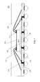
- FIGS. 3 and 4show top and side cross-sectional views of a package 300 , according to an embodiment of the present invention.
- Package 300includes IC die 302 , mold compound 304 , substrate 306 , wirebonds 308 , bond pads 310 , bond fingers 312 , solder balls 314 , contact pads 316 , die attach pad 318 , and leads 320 .
- package 300is a combination of a BGA package, such as BGA package 100 described with reference to FIG. 1 , and a leadframe package, such as leadframe package 200 described with reference to FIG. 2 .
- package 300is referred to herein as a leadframe-ball grid array (LF-BGA) package. Similar to packages 100 and 200 described above, package 300 may be used to mount an IC die onto a PCB.
- LF-BGAleadframe-ball grid array
- IC die 302is coupled to die attach pad 318 through an adhesive 322 a.
- Die attach pad 318is coupled to one or more leads of leads 320 .
- Die attach pad 318is also coupled to substrate 306 through an adhesive 322 b.
- Adhesives 302 a and 302 bmay be thermally and/or electrically conductive.
- Wirebonds 308couple bond pads 310 on the first surface of IC die 302 to bond fingers 312 on substrate 306 , die attach pad 318 , and leads of leads 320 .
- IC die 302then, may be coupled to a PCB through solder balls 314 and/or leads 320 .
- LF-BGA package 300allows for a greater number of I/O connections compared to both BGA package 100 and leadframe package 200 .
- heatmay be transferred from IC die 302 to the PCB in a variety of ways.
- IC die 302is coupled to die attach pad 318 through adhesive 322 a.
- die attach pad 318is often made out of a thermally conductive material such as a metal (e.g., copper).
- adhesive 322 ais a thermally conductive adhesive
- heatmay be transferred from the second surface of IC die 302 to die attach pad 318 .
- FIG. 4shows that die attach pad 318 is coupled to leads of leads 320 such that heat transferred from IC die 302 to die attach pad 318 may be transferred to a PCB through leads of leads 320 .
- heatmay also be transferred from the second surface of IC die 302 through die attach pad 318 , substrate 306 , and to a PCB through contact pads 316 and solder balls 314 .
- the leadframemay function as a heat spreader that spreads heat from IC die 302 .
- heatmay be transferred from the first surface of IC die 302 through wirebonds 308 that are coupled to leads 320 and die attach pad 318 and through wirebonds 308 that are coupled to bond fingers 312 .
- Heat transferred to bond fingers 312may be transferred to a PCB through contact pads 316 and solder balls 314 .
- heatmay be transferred from IC die 302 to the PCB through both leads 320 and solder balls 314 . Therefore, package 300 exhibits increased thermal performance compared to both BGA package 100 and leadframe package 200 .
- LF-BGA package 300Power and ground connections may also be enhanced using LF-BGA package 300 .
- leads of leads 320may be used to provide reliable and stable power and ground connections. As described above, leads 320 typically result in connections that have improved performance when compared to connections formed through high density solder ball connections.
- leads of leads 320may be used to provide high quality power and ground. In such an embodiment, all of solder balls 314 and some leads of leads 320 remain available for other types of connections such as I/O connections.
- LF-BGA package 300allows for high quality supply voltage and ground connections that may be available from leadframe packages such as leadframe package 200 shown in FIG.
- package 300benefits from the increased thermal performance and high quality supply voltage and ground signals that are characteristics of leadframe packages without being significantly more expensive than a BGA package similar to BGA package 100 .
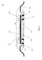
- FIG. 4shows that leads 320 may include two types of leads exemplified by a lead 402 a and a lead 402 b.
- lead 402 ais fused to die attach pad 318 .
- Leads of leads 320 that are similarly fused to die attach pad 318are collectively referred to as leads 402 a for convenience.
- Leads 402 amay be used to provide reliable ground and/or supply voltage connections to IC die 302 .
- IC die 302may be coupled to the high quality signals provided by leads 402 a through wirebonds 404 a. Wirebonds 404 a coupled bond pads 310 on IC die 302 to leads 402 a.
- adhesive 322 ais electrically conductive
- IC die 302is also electrically coupled to leads 402 a through die attach pad 318 .
- FIG. 4also shows lead 402 b that is not fused to die attach pad 318 .
- Leads similar to lead 402 bare collectively referred to as leads 402 b.
- Leads 402 bare not electrically coupled to die attach pad 318 or leads 402 a.
- leads 402 bmay be used to form connections with a PCB for other types of connections, such as I/O connections.
- leads 402 bmay be used to provide high quality connections to the PCB.
- IC die 302may be coupled to leads 402 b through wirebonds 404 b and bond pads 310 .
- IC die 302may also be coupled to a PCB through solder balls 314 .
- Bond pads 310 of IC die 302may be coupled to bond fingers 312 on substrate 306 through wirebonds 404 c and to the PCB through solder balls 314 .
- FIG. 5shows a package 500 , according to an embodiment of the present invention.
- Package 500is substantially similar to package 300 described with reference to FIG. 3 except that solder balls 314 are removed.
- contact pads 316are land grid array (LGA) contacts.
- LGAland grid array
- soldermay be placed on LGA contacts 118 to couple package 500 to the PCB.
- package 500may be termed a leadframe-land grid array (LF-LGA) package that operates substantially similar to a LF-BGA package as described above.
- LF-LGAleadframe-land grid array
- FIG. 6shows a LF-LGA package 600 , according to an embodiment of the present invention.
- LF-LGA package 600is generally similar to LF-LGA package 500 described with reference to FIG. 5 .
- LF-LGA package 600additionally includes a second IC die 602 .
- Second IC die 602is coupled to the first surface of IC die 302 through an adhesive 604 .
- Adhesive 604may be thermally and/or electrically conductive.
- bond pads 606 on a first surface of second IC die 602may be coupled to leads of leads 320 , die attach pad 318 , and substrate 306 through wirebonds 608 .
- LF-LGA package 600allows for two IC die to be included in the same package.
- IC die 302is a memory device and second IC die 602 is an application specific integrated circuit (ASIC).
- ASICapplication specific integrated circuit
- package 600may be configured such that the memory device may interact with the ASIC.
- package 600may be configured such that the memory device and the ASIC are isolated.
- IC die 302 and second IC die 602may be other combinations of memory devices, ASICs, or other elements as would be apparent to those skilled in the relevant art(s).
- FIG. 7shows a stacked die LF-LGA package 700 , according to an embodiment of the present invention.
- Package 700is generally similar to package 600 shown in FIG. 6 . However, instead of including a die up configured second IC die 602 stacked on first IC die 302 , package 700 includes a die down configured second IC die 702 stacked on first IC die 302 . In such a configuration, bond pads 704 of second IC die 702 are coupled to the first surface of IC die 302 .
- second IC die 702may then be coupled to leads 320 , die attach pad 318 , and/or, LGA contacts 118 through traces formed on the first surface of IC die 302 and wirebonds 308 and/or through IC die 302 . Additionally or alternatively, second IC die 702 may interact with first IC die 302 through bond pads 704 .
- second IC die 702may be a memory associated with IC die 302 . In such an embodiment, the contents of second IC die 702 (i.e., the memory) may be directly accessed by IC die 302 through bond pads 704 .
- second IC die 702may be a power management unit (PMU) configured to manage power used by IC die 302 .
- PMUpower management unit
- IC die 302 and second IC die 702may be any combination of memory devices, ASICs, PMUs, or other intergrated circuit devices, as would be appreciated by those skilled in the relevant art(s).
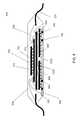
- FIG. 8shows a stacked die LF-LGA package 800 , according to an embodiment of present invention.
- Stacked die LF-LGA package 800is generally similar to stacked die LF-LGA package 700 shown in FIG. 7 .
- package 800additionally includes a third IC die 802 and a fourth IC die 804 .
- both third IC die 802 and fourth IC die 804are implemented in die down configurations.
- Third IC die 802 and fourth IC die 804are coupled to substrate 306 through bond pads 806 and bond pads 808 formed on first surfaces of third IC die 802 and fourth IC die 804 , respectively.
- third IC die 802 and fourth IC die 804are electrically coupled to a PCB to which package 800 is attached.
- third IC die 802 and fourth IC die 804may be implemented in a die-up configuration.
- wirebondsmay couple bond pads on third IC die 802 and fourth IC die 804 to substrate 306 , die attach pad 318 , leads of leads 320 , IC die 302 , and/or second IC die 702 .
- Heatmay be transferred from the first surfaces third IC die 802 and fourth IC die 804 through substrate 306 . Additionally, die attach pad 318 is coupled to second surfaces of third IC die 802 and fourth IC die 804 through adhesive 322 b. Thus, heat may also be conducted away from third IC die 802 and fourth IC die 804 through lead of leads 320 that are coupled to die attach pad 204 .
- IC die 302 , second IC die 702 , third IC die 802 , and fourth IC die 804may be any combination of ASICs, memory devices, system in package (SIP) ICs, and/or PMUs as would be appreciated by those skilled in the relevant art(s).
- SIPsystem in package
- Packages 600 , 700 , and 800are shown to be a stacked die LF-LGA packages. As would appreciated by those skilled in the relevant art(s), similar stacked die packages may also be implemented as LF-BGA packages in which contact pads 316 are solder ball pads and solder balls are formed thereon, without departing from the scope and spirit of the invention.
- FIG. 9shows a flowchart 900 providing example steps for assembling an IC package.
- Other structural and operational embodimentswill be apparent to persons skilled in the relevant art(s) based on the following discussion.
- the steps shown in FIG. 9do not necessarily have to occur in the order shown.
- the steps of FIG. 9are described in detail below.
- Flowchart 900begins in step 902 .
- a leadframeis formed.
- a leadframeis formed so as to include die attach pad 318 and leads 320 .
- Leads 320emanate in an outward direction from die attach pad 318 .
- leads 320may include leads 402 a that are coupled to die attach pad 318 and leads 402 b that are not coupled to die attach pad 318 .
- an IC dieis coupled to a die attach pad.
- IC die 302is coupled to die attach pad 318 through adhesive 322 a.
- Adhesive 322 amay be thermally and/or electrically conductive.
- a substrateis coupled to the die attach pad.
- substrate 306is coupled to die attach pad 318 through adhesive 322 b.
- Adhesive 322 bmay be thermally and/or electrically conductive.
- wirebondsare formed.
- Wirebondsmay couple bond pads on a first surface of the IC die to one or more leads, the die attach pad, and/or bond fingers on the substrate.
- wirebonds 308coupled bond pads 310 to one or more leads of leads 320 , die attach pad 318 , and bond fingers 312 on substrate 306 .
- solder ballsare formed. Solder balls may be formed on solder ball pads on the substrate. The solder balls may facilitate mounting of the IC package on to a printed circuit board (PCB). For example, in FIG. 3 , solder balls 314 are formed on contact pads 316 . In alternate embodiments, contact pads 316 may be land grid array (LGA) contacts that facilitate mounting the package on to a PCB.
- LGAland grid array
- step 912the IC die, wirebonds, die attach pad, and a portion of each lead are encapsulated in a mold material.
- IC die 302 , wirebonds 308 , die attach pad 318 , and a portion of each lead of leads 320are encapsulated in mold compound 304 .
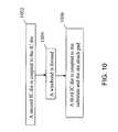
- FIG. 10provides optional steps for flowchart 900 .
- FIG. 10shows steps 1002 , 1004 , and 1006 .
- a second IC dieis coupled to the IC die.
- second IC die 602is coupled to IC die 302 through adhesive 604 in a die-up configuration.
- second IC die 702may be configured in a die-down configuration.
- a wirebondis formed.
- the wirebondsmay couple bond pads on the second IC die to the IC die, the die attach pad, one or more leads, and/or the substrate.
- wirebonds 608couple bond pads 606 to IC die 302 , die attach pad 318 , one or more leads of leads 320 , and/or substrate 306 .
- the second IC diemay be configured in a die-down configuration in which contact pads on the second IC die are coupled to the IC die.
- a third IC dieis coupled to the substrate and the die attach pad.
- third IC die 802is coupled to substrate 306 through contacts 806 and to die attach pad 318 through adhesive 322 b.
Landscapes
- Engineering & Computer Science (AREA)
- Microelectronics & Electronic Packaging (AREA)
- Physics & Mathematics (AREA)
- Condensed Matter Physics & Semiconductors (AREA)
- General Physics & Mathematics (AREA)
- Computer Hardware Design (AREA)
- Power Engineering (AREA)
- Wire Bonding (AREA)
Abstract
Description
Claims (22)
Priority Applications (1)
| Application Number | Priority Date | Filing Date | Title |
|---|---|---|---|
| US11/987,452US7872335B2 (en) | 2007-06-08 | 2007-11-30 | Lead frame-BGA package with enhanced thermal performance and I/O counts |
Applications Claiming Priority (2)
| Application Number | Priority Date | Filing Date | Title |
|---|---|---|---|
| US92901907P | 2007-06-08 | 2007-06-08 | |
| US11/987,452US7872335B2 (en) | 2007-06-08 | 2007-11-30 | Lead frame-BGA package with enhanced thermal performance and I/O counts |
Publications (2)
| Publication Number | Publication Date |
|---|---|
| US20080303124A1 US20080303124A1 (en) | 2008-12-11 |
| US7872335B2true US7872335B2 (en) | 2011-01-18 |
Family
ID=40095075
Family Applications (1)
| Application Number | Title | Priority Date | Filing Date |
|---|---|---|---|
| US11/987,452Active2029-03-16US7872335B2 (en) | 2007-06-08 | 2007-11-30 | Lead frame-BGA package with enhanced thermal performance and I/O counts |
Country Status (1)
| Country | Link |
|---|---|
| US (1) | US7872335B2 (en) |
Cited By (31)
| Publication number | Priority date | Publication date | Assignee | Title |
|---|---|---|---|---|
| US20110175212A1 (en)* | 2010-01-20 | 2011-07-21 | Freescale Semiconductor, Inc. | Dual die semiconductor package |
| US8643189B1 (en) | 2012-07-17 | 2014-02-04 | Freescale Semiconductor, Inc. | Packaged semiconductor die with power rail pads |
| US9362212B1 (en) | 2015-03-12 | 2016-06-07 | Freescale Semiconductor, Inc. | Integrated circuit package having side and bottom contact pads |
| US9812402B2 (en) | 2015-10-12 | 2017-11-07 | Invensas Corporation | Wire bond wires for interference shielding |
| US9842745B2 (en) | 2012-02-17 | 2017-12-12 | Invensas Corporation | Heat spreading substrate with embedded interconnects |
| US9852969B2 (en) | 2013-11-22 | 2017-12-26 | Invensas Corporation | Die stacks with one or more bond via arrays of wire bond wires and with one or more arrays of bump interconnects |
| US9888579B2 (en) | 2015-03-05 | 2018-02-06 | Invensas Corporation | Pressing of wire bond wire tips to provide bent-over tips |
| US9911718B2 (en) | 2015-11-17 | 2018-03-06 | Invensas Corporation | ‘RDL-First’ packaged microelectronic device for a package-on-package device |
| US9935075B2 (en) | 2016-07-29 | 2018-04-03 | Invensas Corporation | Wire bonding method and apparatus for electromagnetic interference shielding |
| US9953914B2 (en) | 2012-05-22 | 2018-04-24 | Invensas Corporation | Substrate-less stackable package with wire-bond interconnect |
| US9984992B2 (en) | 2015-12-30 | 2018-05-29 | Invensas Corporation | Embedded wire bond wires for vertical integration with separate surface mount and wire bond mounting surfaces |
| US10008469B2 (en) | 2015-04-30 | 2018-06-26 | Invensas Corporation | Wafer-level packaging using wire bond wires in place of a redistribution layer |
| US10008477B2 (en) | 2013-09-16 | 2018-06-26 | Invensas Corporation | Microelectronic element with bond elements to encapsulation surface |
| US10026717B2 (en) | 2013-11-22 | 2018-07-17 | Invensas Corporation | Multiple bond via arrays of different wire heights on a same substrate |
| US10062661B2 (en) | 2011-05-03 | 2018-08-28 | Tessera, Inc. | Package-on-package assembly with wire bonds to encapsulation surface |
| US10128216B2 (en) | 2010-07-19 | 2018-11-13 | Tessera, Inc. | Stackable molded microelectronic packages |
| US10181457B2 (en) | 2015-10-26 | 2019-01-15 | Invensas Corporation | Microelectronic package for wafer-level chip scale packaging with fan-out |
| US10199364B2 (en) | 2016-05-19 | 2019-02-05 | Sanmina Corporation | Non-volatile dual in-line memory module (NVDIMM) multichip package |
| US10299368B2 (en) | 2016-12-21 | 2019-05-21 | Invensas Corporation | Surface integrated waveguides and circuit structures therefor |
| US10297582B2 (en) | 2012-08-03 | 2019-05-21 | Invensas Corporation | BVA interposer |
| US20190164807A1 (en)* | 2017-11-27 | 2019-05-30 | Texas Instruments Incorporated | Electronic package for integrated circuits and related methods |
| US10332854B2 (en) | 2015-10-23 | 2019-06-25 | Invensas Corporation | Anchoring structure of fine pitch bva |
| US10381326B2 (en) | 2014-05-28 | 2019-08-13 | Invensas Corporation | Structure and method for integrated circuits packaging with increased density |
| US10460958B2 (en) | 2013-08-07 | 2019-10-29 | Invensas Corporation | Method of manufacturing embedded packaging with preformed vias |
| US10529636B2 (en) | 2014-01-17 | 2020-01-07 | Invensas Corporation | Fine pitch BVA using reconstituted wafer with area array accessible for testing |
| US10707153B2 (en) | 2016-04-29 | 2020-07-07 | Stmicroelectronics S.R.L. | Semiconductor device having die pad |
| US10756049B2 (en) | 2011-10-17 | 2020-08-25 | Invensas Corporation | Package-on-package assembly with wire bond vias |
| US20220221353A1 (en)* | 2021-01-12 | 2022-07-14 | Texas Instruments Incorporated | Semiconductor force sensors |
| US11498831B2 (en) | 2016-01-13 | 2022-11-15 | Texas Instruments Incorporated | Structures for packaging stress-sensitive micro-electro-mechanical system stacked onto electronic circuit chip |
| US11538767B2 (en) | 2017-12-29 | 2022-12-27 | Texas Instruments Incorporated | Integrated circuit package with partitioning based on environmental sensitivity |
| US11869837B2 (en) | 2021-07-22 | 2024-01-09 | Nxp B.V. | Semiconductor device packaging extendable lead and method therefor |
Families Citing this family (12)
| Publication number | Priority date | Publication date | Assignee | Title |
|---|---|---|---|---|
| US7875965B2 (en)* | 2008-03-18 | 2011-01-25 | Mediatek Inc. | Semiconductor chip package |
| US7834436B2 (en)* | 2008-03-18 | 2010-11-16 | Mediatek Inc. | Semiconductor chip package |
| US8018037B2 (en)* | 2009-04-16 | 2011-09-13 | Mediatek Inc. | Semiconductor chip package |
| US20100314730A1 (en)* | 2009-06-16 | 2010-12-16 | Broadcom Corporation | Stacked hybrid interposer through silicon via (TSV) package |
| US8884630B2 (en) | 2009-07-24 | 2014-11-11 | Hewlett-Packard Development Company, L.P. | Active pin connection monitoring system and method |
| CN102804940A (en)* | 2009-09-24 | 2012-11-28 | 奥普蒂恩公司 | Layout of contact pads of a system in package, comprising circuit board and electronic integrated elements |
| US8547709B2 (en) | 2010-02-12 | 2013-10-01 | Cyntec Co. Ltd. | Electronic system with a composite substrate |
| US9559064B2 (en)* | 2013-12-04 | 2017-01-31 | Taiwan Semiconductor Manufacturing Company, Ltd. | Warpage control in package-on-package structures |
| US10490528B2 (en)* | 2015-10-12 | 2019-11-26 | Invensas Corporation | Embedded wire bond wires |
| US11302611B2 (en)* | 2018-11-28 | 2022-04-12 | Texas Instruments Incorporated | Semiconductor package with top circuit and an IC with a gap over the IC |
| CN114068470A (en)* | 2021-11-16 | 2022-02-18 | 华进半导体封装先导技术研发中心有限公司 | A structure for expanding the I/O port of a ball grid array package and a manufacturing method thereof |
| CN118712161B (en)* | 2024-08-29 | 2024-11-08 | 深圳市联润丰电子科技有限公司 | High-density high-firmness packaging structure and performance detection method thereof |
Citations (80)
| Publication number | Priority date | Publication date | Assignee | Title |
|---|---|---|---|---|
| US4480262A (en) | 1982-07-15 | 1984-10-30 | Olin Corporation | Semiconductor casing |
| US4560826A (en) | 1983-12-29 | 1985-12-24 | Amp Incorporated | Hermetically sealed chip carrier |
| US4680613A (en) | 1983-12-01 | 1987-07-14 | Fairchild Semiconductor Corporation | Low impedance package for integrated circuit die |
| US4803544A (en) | 1986-07-11 | 1989-02-07 | Junghans Uhren Gmbh | Prefabricated strip conductor network assembly unit and process for making same |
| US5105260A (en) | 1989-10-31 | 1992-04-14 | Sgs-Thomson Microelectronics, Inc. | Rf transistor package with nickel oxide barrier |
| US5153379A (en) | 1990-10-09 | 1992-10-06 | Motorola, Inc. | Shielded low-profile electronic component assembly |
| US5294826A (en) | 1993-04-16 | 1994-03-15 | Northern Telecom Limited | Integrated circuit package and assembly thereof for thermal and EMI management |
| US5350943A (en) | 1992-04-18 | 1994-09-27 | Temic Telefunken Microelectronic Gmbh | Semiconductor assembly, in particular a remote control reception module |
| US5376756A (en) | 1991-12-20 | 1994-12-27 | Vlsi Technology, Inc. | Wire support and guide |
| US5386141A (en)* | 1992-03-31 | 1995-01-31 | Vlsi Technology, Inc. | Leadframe having one or more power/ground planes without vias |
| US5389816A (en) | 1992-11-19 | 1995-02-14 | Shinko Electric Industries Co., Ltd. | Multi-layer lead frame using a metal-core substrate |
| US5468910A (en) | 1993-08-02 | 1995-11-21 | Motorola, Inc. | Semiconductor device package and method of making |
| US5486720A (en) | 1994-05-26 | 1996-01-23 | Analog Devices, Inc. | EMF shielding of an integrated circuit package |
| US5497032A (en) | 1993-03-17 | 1996-03-05 | Fujitsu Limited | Semiconductor device and lead frame therefore |
| US5559306A (en) | 1994-05-17 | 1996-09-24 | Olin Corporation | Electronic package with improved electrical performance |
| US5596225A (en)* | 1994-10-27 | 1997-01-21 | National Semiconductor Corporation | Leadframe for an integrated circuit package which electrically interconnects multiple integrated circuit die |
| US5608265A (en) | 1993-03-17 | 1997-03-04 | Hitachi, Ltd. | Encapsulated semiconductor device package having holes for electrically conductive material |
| US5642261A (en) | 1993-12-20 | 1997-06-24 | Sgs-Thomson Microelectronics, Inc. | Ball-grid-array integrated circuit package with solder-connected thermal conductor |
| US5650659A (en) | 1995-08-04 | 1997-07-22 | National Semiconductor Corporation | Semiconductor component package assembly including an integral RF/EMI shield |
| US5668406A (en) | 1994-05-31 | 1997-09-16 | Nec Corporation | Semiconductor device having shielding structure made of electrically conductive paste |
| US5889316A (en) | 1993-06-18 | 1999-03-30 | Space Electronics, Inc. | Radiation shielding of plastic integrated circuits |
| US5977626A (en) | 1998-08-12 | 1999-11-02 | Industrial Technology Research Institute | Thermally and electrically enhanced PBGA package |
| US5986340A (en) | 1996-05-02 | 1999-11-16 | National Semiconductor Corporation | Ball grid array package with enhanced thermal and electrical characteristics and electronic device incorporating same |
| US6011303A (en) | 1996-11-29 | 2000-01-04 | Nec Corporation | Electronic component |
| US6020624A (en)* | 1991-06-04 | 2000-02-01 | Micron Technology, Inc. | Semiconductor package with bi-substrate die |
| US6092281A (en) | 1998-08-28 | 2000-07-25 | Amkor Technology, Inc. | Electromagnetic interference shield driver and method |
| US6229702B1 (en) | 1999-06-02 | 2001-05-08 | Advanced Semiconductor Engineering, Inc. | Ball grid array semiconductor package having improved heat dissipation efficiency, overall electrical performance and enhanced bonding capability |
| US20020024137A1 (en) | 2000-08-08 | 2002-02-28 | Lars-Anders Olofsson | Method of securing solder balls and any components fixed to one and the same side of a substrate |
| US6376914B2 (en)* | 1999-12-09 | 2002-04-23 | Atmel Corporation | Dual-die integrated circuit package |
| US6395582B1 (en) | 1997-07-14 | 2002-05-28 | Signetics | Methods for forming ground vias in semiconductor packages |
| US20020079572A1 (en) | 2000-12-22 | 2002-06-27 | Khan Reza-Ur Rahman | Enhanced die-up ball grid array and method for making the same |
| US6432742B1 (en) | 2000-08-17 | 2002-08-13 | St Assembly Test Services Pte Ltd. | Methods of forming drop-in heat spreader plastic ball grid array (PBGA) packages |
| US6501184B1 (en) | 1999-05-20 | 2002-12-31 | Amkor Technology, Inc. | Semiconductor package and method for manufacturing the same |
| US6528876B2 (en) | 2000-06-26 | 2003-03-04 | Siliconware Precision Industries Co., Ltd. | Semiconductor package having heat sink attached to substrate |
| US20030057550A1 (en) | 2000-12-22 | 2003-03-27 | Broadcom Corporation | Ball grid array package enhanced with a thermal and electrical connector |
| US6552428B1 (en) | 1998-10-12 | 2003-04-22 | Siliconware Precision Industries Co., Ltd. | Semiconductor package having an exposed heat spreader |
| US20030111728A1 (en) | 2001-09-26 | 2003-06-19 | Thai Cao Minh | Mounting material, semiconductor device and method of manufacturing semiconductor device |
| US20030146509A1 (en) | 2002-02-01 | 2003-08-07 | Broadcom Corporation | Ball grid array package with separated stiffener layer |
| US6614102B1 (en) | 2001-05-04 | 2003-09-02 | Amkor Technology, Inc. | Shielded semiconductor leadframe package |
| US6617200B2 (en) | 2000-07-05 | 2003-09-09 | Seiko Epson Corporation | System and method for fabricating a semiconductor device |
| US20030178719A1 (en) | 2002-03-22 | 2003-09-25 | Combs Edward G. | Enhanced thermal dissipation integrated circuit package and method of manufacturing enhanced thermal dissipation integrated circuit package |
| US20040038447A1 (en) | 2002-08-21 | 2004-02-26 | Corisis David J | Packaged microelectronic devices and methods for assembling microelectronic devices |
| US6707140B1 (en) | 2000-05-09 | 2004-03-16 | National Semiconductor Corporation | Arrayable, scaleable, and stackable molded package configuration |
| US20040084771A1 (en) | 2002-11-05 | 2004-05-06 | Micron Technology, Inc. | Methods and apparatus for a thin stacked ball-grid array package |
| US6737750B1 (en) | 2001-12-07 | 2004-05-18 | Amkor Technology, Inc. | Structures for improving heat dissipation in stacked semiconductor packages |
| US6775140B2 (en) | 2002-10-21 | 2004-08-10 | St Assembly Test Services Ltd. | Heat spreaders, heat spreader packages, and fabrication methods for use with flip chip semiconductor devices |
| US20040178499A1 (en) | 2003-03-10 | 2004-09-16 | Mistry Addi B. | Semiconductor package with multiple sides having package contacts |
| US6825108B2 (en) | 2002-02-01 | 2004-11-30 | Broadcom Corporation | Ball grid array package fabrication with IC die support structures |
| US6838761B2 (en) | 2002-09-17 | 2005-01-04 | Chippac, Inc. | Semiconductor multi-package module having wire bond interconnect between stacked packages and having electrical shield |
| US6853070B2 (en) | 2001-02-15 | 2005-02-08 | Broadcom Corporation | Die-down ball grid array package with die-attached heat spreader and method for making the same |
| US20050035452A1 (en) | 2001-05-07 | 2005-02-17 | Broadcom Corporation | Die-up ball grid array package including a substrate having an opening and method for making the same |
| US6861288B2 (en)* | 2003-01-23 | 2005-03-01 | St Assembly Test Services, Ltd. | Stacked semiconductor packages and method for the fabrication thereof |
| US20050077545A1 (en) | 2000-12-01 | 2005-04-14 | Broadcom Corporation | Ball grid array package with patterned stiffener surface and method of assembling the same |
| US6906414B2 (en) | 2000-12-22 | 2005-06-14 | Broadcom Corporation | Ball grid array package with patterned stiffener layer |
| US20050127501A1 (en) | 2001-12-18 | 2005-06-16 | Broadcom Corporation | Ball grid array package substrates with a modified central opening and method for making the same |
| US6919630B2 (en) | 2003-03-27 | 2005-07-19 | Siliconware Precision Industries Co. Ltd. | Semiconductor package with heat spreader |
| US6951982B2 (en)* | 2002-11-22 | 2005-10-04 | Micron Technology, Inc. | Packaged microelectronic component assemblies |
| US20050280141A1 (en) | 2004-06-21 | 2005-12-22 | Broadcom Corporation | Integrated circuit device package having both wire bond and flip-chip interconnections and method of making the same |
| US20050280139A1 (en) | 2004-06-21 | 2005-12-22 | Broadcom Corporation | Multipiece apparatus for thermal and electromagnetic interference (EMI) shielding enhancement in die-up array packages and method of making the same |
| US20050280127A1 (en) | 2004-06-21 | 2005-12-22 | Broadcom Corporation | Apparatus and method for thermal and electromagnetic interference (EMI) shielding enhancement in die-up array packages |
| US20060012037A1 (en) | 2004-07-01 | 2006-01-19 | Raedt Walter D | Methods for bonding and devices according to such methods |
| US7015072B2 (en) | 2001-07-11 | 2006-03-21 | Asat Limited | Method of manufacturing an enhanced thermal dissipation integrated circuit package |
| US7026711B2 (en) | 2003-12-16 | 2006-04-11 | Taiwan Semiconductor Manufacturing Company, Ltd. | Thermal dispensing enhancement for high performance flip chip BGA (HPFCBGA) |
| US7057277B2 (en) | 2003-04-22 | 2006-06-06 | Industrial Technology Research Institute | Chip package structure |
| US7061102B2 (en) | 2001-06-11 | 2006-06-13 | Xilinx, Inc. | High performance flipchip package that incorporates heat removal with minimal thermal mismatch |
| US20060166397A1 (en) | 2002-09-30 | 2006-07-27 | Lau Daniel K | Thermal enhanced package for block mold assembly |
| US7132744B2 (en) | 2000-12-22 | 2006-11-07 | Broadcom Corporation | Enhanced die-up ball grid array packages and method for making the same |
| US7148084B2 (en) | 1994-04-01 | 2006-12-12 | Maxwell Technologies, Inc. | Radiation shielding of integrated circuits and multi-chip modules in ceramic and metal packages |
| US7198987B1 (en) | 2004-03-04 | 2007-04-03 | Skyworks Solutions, Inc. | Overmolded semiconductor package with an integrated EMI and RFI shield |
| US20070090502A1 (en) | 2005-10-20 | 2007-04-26 | Broadcom Corporation | Methods and apparatus for improved thermal performance and electromagnetic interference (EMI) shielding in leadframe integrated circuit (IC) packages |
| US20070170570A1 (en)* | 2006-01-24 | 2007-07-26 | Stats Chippac Ltd. | Integrated circuit package system including wide flange leadframe |
| US20070200210A1 (en) | 2006-02-28 | 2007-08-30 | Broadcom Corporation | Methods and apparatus for improved thermal performance and electromagnetic interference (EMI) shielding in integrated circuit (IC) packages |
| US20070267734A1 (en) | 2006-05-16 | 2007-11-22 | Broadcom Corporation | No-lead IC packages having integrated heat spreader for electromagnetic interference (EMI) shielding and thermal enhancement |
| US20070267740A1 (en) | 2006-05-16 | 2007-11-22 | Broadcom Corporation | Method and apparatus for cooling semiconductor device hot blocks and large scale integrated circuit (IC) using integrated interposer for IC packages |
| US20070273023A1 (en) | 2006-05-26 | 2007-11-29 | Broadcom Corporation | Integrated circuit package having exposed thermally conducting body |
| US20070273049A1 (en) | 2006-05-12 | 2007-11-29 | Broadcom Corporation | Interconnect structure and formation for package stacking of molded plastic area array package |
| US20070278632A1 (en) | 2006-06-01 | 2007-12-06 | Broadcom Corporation | Leadframe IC packages having top and bottom integrated heat spreaders |
| US20070290376A1 (en) | 2006-06-20 | 2007-12-20 | Broadcom Corporation | Integrated circuit (IC) package stacking and IC packages formed by same |
| US20070290322A1 (en) | 2006-06-20 | 2007-12-20 | Broadcom Corporation | Thermal improvement for hotspots on dies in integrated circuit packages |
| US20080054432A1 (en)* | 2006-09-01 | 2008-03-06 | Corisis David J | High density stacked die assemblies, structures incorporated therein and methods of fabricating the assemblies |
Family Cites Families (1)
| Publication number | Priority date | Publication date | Assignee | Title |
|---|---|---|---|---|
| US5977636A (en)* | 1997-01-17 | 1999-11-02 | Micron Technology, Inc. | Method of forming an electrically conductive contact plug, method of forming a reactive or diffusion barrier layer over a substrate, integrated circuitry, and method of forming a layer of titanium boride |
- 2007
- 2007-11-30USUS11/987,452patent/US7872335B2/enactiveActive
Patent Citations (95)
| Publication number | Priority date | Publication date | Assignee | Title |
|---|---|---|---|---|
| US4480262A (en) | 1982-07-15 | 1984-10-30 | Olin Corporation | Semiconductor casing |
| US4680613A (en) | 1983-12-01 | 1987-07-14 | Fairchild Semiconductor Corporation | Low impedance package for integrated circuit die |
| US4560826A (en) | 1983-12-29 | 1985-12-24 | Amp Incorporated | Hermetically sealed chip carrier |
| US4803544A (en) | 1986-07-11 | 1989-02-07 | Junghans Uhren Gmbh | Prefabricated strip conductor network assembly unit and process for making same |
| US5105260A (en) | 1989-10-31 | 1992-04-14 | Sgs-Thomson Microelectronics, Inc. | Rf transistor package with nickel oxide barrier |
| US5153379A (en) | 1990-10-09 | 1992-10-06 | Motorola, Inc. | Shielded low-profile electronic component assembly |
| US6020624A (en)* | 1991-06-04 | 2000-02-01 | Micron Technology, Inc. | Semiconductor package with bi-substrate die |
| US5376756A (en) | 1991-12-20 | 1994-12-27 | Vlsi Technology, Inc. | Wire support and guide |
| US5386141A (en)* | 1992-03-31 | 1995-01-31 | Vlsi Technology, Inc. | Leadframe having one or more power/ground planes without vias |
| US5350943A (en) | 1992-04-18 | 1994-09-27 | Temic Telefunken Microelectronic Gmbh | Semiconductor assembly, in particular a remote control reception module |
| US5389816A (en) | 1992-11-19 | 1995-02-14 | Shinko Electric Industries Co., Ltd. | Multi-layer lead frame using a metal-core substrate |
| US5497032A (en) | 1993-03-17 | 1996-03-05 | Fujitsu Limited | Semiconductor device and lead frame therefore |
| US5608265A (en) | 1993-03-17 | 1997-03-04 | Hitachi, Ltd. | Encapsulated semiconductor device package having holes for electrically conductive material |
| US5294826A (en) | 1993-04-16 | 1994-03-15 | Northern Telecom Limited | Integrated circuit package and assembly thereof for thermal and EMI management |
| US5889316A (en) | 1993-06-18 | 1999-03-30 | Space Electronics, Inc. | Radiation shielding of plastic integrated circuits |
| US5468910A (en) | 1993-08-02 | 1995-11-21 | Motorola, Inc. | Semiconductor device package and method of making |
| US5642261A (en) | 1993-12-20 | 1997-06-24 | Sgs-Thomson Microelectronics, Inc. | Ball-grid-array integrated circuit package with solder-connected thermal conductor |
| US7148084B2 (en) | 1994-04-01 | 2006-12-12 | Maxwell Technologies, Inc. | Radiation shielding of integrated circuits and multi-chip modules in ceramic and metal packages |
| US5559306A (en) | 1994-05-17 | 1996-09-24 | Olin Corporation | Electronic package with improved electrical performance |
| US5486720A (en) | 1994-05-26 | 1996-01-23 | Analog Devices, Inc. | EMF shielding of an integrated circuit package |
| US5668406A (en) | 1994-05-31 | 1997-09-16 | Nec Corporation | Semiconductor device having shielding structure made of electrically conductive paste |
| US5596225A (en)* | 1994-10-27 | 1997-01-21 | National Semiconductor Corporation | Leadframe for an integrated circuit package which electrically interconnects multiple integrated circuit die |
| US5650659A (en) | 1995-08-04 | 1997-07-22 | National Semiconductor Corporation | Semiconductor component package assembly including an integral RF/EMI shield |
| US5986340A (en) | 1996-05-02 | 1999-11-16 | National Semiconductor Corporation | Ball grid array package with enhanced thermal and electrical characteristics and electronic device incorporating same |
| US6011303A (en) | 1996-11-29 | 2000-01-04 | Nec Corporation | Electronic component |
| US6395582B1 (en) | 1997-07-14 | 2002-05-28 | Signetics | Methods for forming ground vias in semiconductor packages |
| US5977626A (en) | 1998-08-12 | 1999-11-02 | Industrial Technology Research Institute | Thermally and electrically enhanced PBGA package |
| US6092281A (en) | 1998-08-28 | 2000-07-25 | Amkor Technology, Inc. | Electromagnetic interference shield driver and method |
| US6552428B1 (en) | 1998-10-12 | 2003-04-22 | Siliconware Precision Industries Co., Ltd. | Semiconductor package having an exposed heat spreader |
| US6501184B1 (en) | 1999-05-20 | 2002-12-31 | Amkor Technology, Inc. | Semiconductor package and method for manufacturing the same |
| US6229702B1 (en) | 1999-06-02 | 2001-05-08 | Advanced Semiconductor Engineering, Inc. | Ball grid array semiconductor package having improved heat dissipation efficiency, overall electrical performance and enhanced bonding capability |
| US6376914B2 (en)* | 1999-12-09 | 2002-04-23 | Atmel Corporation | Dual-die integrated circuit package |
| US6707140B1 (en) | 2000-05-09 | 2004-03-16 | National Semiconductor Corporation | Arrayable, scaleable, and stackable molded package configuration |
| US6528876B2 (en) | 2000-06-26 | 2003-03-04 | Siliconware Precision Industries Co., Ltd. | Semiconductor package having heat sink attached to substrate |
| US6617200B2 (en) | 2000-07-05 | 2003-09-09 | Seiko Epson Corporation | System and method for fabricating a semiconductor device |
| US20020024137A1 (en) | 2000-08-08 | 2002-02-28 | Lars-Anders Olofsson | Method of securing solder balls and any components fixed to one and the same side of a substrate |
| US6432742B1 (en) | 2000-08-17 | 2002-08-13 | St Assembly Test Services Pte Ltd. | Methods of forming drop-in heat spreader plastic ball grid array (PBGA) packages |
| US20050077545A1 (en) | 2000-12-01 | 2005-04-14 | Broadcom Corporation | Ball grid array package with patterned stiffener surface and method of assembling the same |
| US6989593B2 (en) | 2000-12-22 | 2006-01-24 | Broadcom Corporation | Die-up ball grid array package with patterned stiffener opening |
| US20070007644A1 (en) | 2000-12-22 | 2007-01-11 | Broadcom Corporation | Ball grid array package enhanced with a thermal and electrical connector |
| US20030057550A1 (en) | 2000-12-22 | 2003-03-27 | Broadcom Corporation | Ball grid array package enhanced with a thermal and electrical connector |
| US7102225B2 (en) | 2000-12-22 | 2006-09-05 | Broadcom Corporation | Die-up ball grid array package with printed circuit board attachable heat spreader |
| US7227256B2 (en) | 2000-12-22 | 2007-06-05 | Broadcom Corporation | Die-up ball grid array package with printed circuit board attachable heat spreader |
| US20020190361A1 (en) | 2000-12-22 | 2002-12-19 | Zhao Sam Z. | Die-up ball grid array package with die-attached heat spreader |
| US7202559B2 (en) | 2000-12-22 | 2007-04-10 | Broadcom Corporation | Method of assembling a ball grid array package with patterned stiffener layer |
| US7005737B2 (en) | 2000-12-22 | 2006-02-28 | Broadcom Corporation | Die-up ball grid array package with enhanced stiffener |
| US20070045824A1 (en) | 2000-12-22 | 2007-03-01 | Broadcom Corporation | Methods of making a die-up ball grid array package with printed circuit board attachable heat spreader |
| US20020079572A1 (en) | 2000-12-22 | 2002-06-27 | Khan Reza-Ur Rahman | Enhanced die-up ball grid array and method for making the same |
| US7161239B2 (en) | 2000-12-22 | 2007-01-09 | Broadcom Corporation | Ball grid array package enhanced with a thermal and electrical connector |
| US7038312B2 (en) | 2000-12-22 | 2006-05-02 | Broadcom Corporation | Die-up ball grid array package with attached stiffener ring |
| US20050029657A1 (en) | 2000-12-22 | 2005-02-10 | Broadcom Corporation | Enhanced die-up ball grid array and method for making the same |
| US6906414B2 (en) | 2000-12-22 | 2005-06-14 | Broadcom Corporation | Ball grid array package with patterned stiffener layer |
| US7132744B2 (en) | 2000-12-22 | 2006-11-07 | Broadcom Corporation | Enhanced die-up ball grid array packages and method for making the same |
| US6853070B2 (en) | 2001-02-15 | 2005-02-08 | Broadcom Corporation | Die-down ball grid array package with die-attached heat spreader and method for making the same |
| US6614102B1 (en) | 2001-05-04 | 2003-09-02 | Amkor Technology, Inc. | Shielded semiconductor leadframe package |
| US7259457B2 (en) | 2001-05-07 | 2007-08-21 | Broadcom Corporation | Die-up ball grid array package including a substrate capable of mounting an integrated circuit die and method for making the same |
| US20050035452A1 (en) | 2001-05-07 | 2005-02-17 | Broadcom Corporation | Die-up ball grid array package including a substrate having an opening and method for making the same |
| US7259448B2 (en) | 2001-05-07 | 2007-08-21 | Broadcom Corporation | Die-up ball grid array package with a heat spreader and method for making the same |
| US7061102B2 (en) | 2001-06-11 | 2006-06-13 | Xilinx, Inc. | High performance flipchip package that incorporates heat removal with minimal thermal mismatch |
| US7015072B2 (en) | 2001-07-11 | 2006-03-21 | Asat Limited | Method of manufacturing an enhanced thermal dissipation integrated circuit package |
| US20030111728A1 (en) | 2001-09-26 | 2003-06-19 | Thai Cao Minh | Mounting material, semiconductor device and method of manufacturing semiconductor device |
| US6737750B1 (en) | 2001-12-07 | 2004-05-18 | Amkor Technology, Inc. | Structures for improving heat dissipation in stacked semiconductor packages |
| US20050127501A1 (en) | 2001-12-18 | 2005-06-16 | Broadcom Corporation | Ball grid array package substrates with a modified central opening and method for making the same |
| US7078806B2 (en) | 2002-02-01 | 2006-07-18 | Broadcom Corporation | IC die support structures for ball grid array package fabrication |
| US20030146509A1 (en) | 2002-02-01 | 2003-08-07 | Broadcom Corporation | Ball grid array package with separated stiffener layer |
| US6825108B2 (en) | 2002-02-01 | 2004-11-30 | Broadcom Corporation | Ball grid array package fabrication with IC die support structures |
| US20030178719A1 (en) | 2002-03-22 | 2003-09-25 | Combs Edward G. | Enhanced thermal dissipation integrated circuit package and method of manufacturing enhanced thermal dissipation integrated circuit package |
| US20040038447A1 (en) | 2002-08-21 | 2004-02-26 | Corisis David J | Packaged microelectronic devices and methods for assembling microelectronic devices |
| US6838761B2 (en) | 2002-09-17 | 2005-01-04 | Chippac, Inc. | Semiconductor multi-package module having wire bond interconnect between stacked packages and having electrical shield |
| US20060166397A1 (en) | 2002-09-30 | 2006-07-27 | Lau Daniel K | Thermal enhanced package for block mold assembly |
| US7259445B2 (en) | 2002-09-30 | 2007-08-21 | Advanced Interconnect Technologies Limited | Thermal enhanced package for block mold assembly |
| US6775140B2 (en) | 2002-10-21 | 2004-08-10 | St Assembly Test Services Ltd. | Heat spreaders, heat spreader packages, and fabrication methods for use with flip chip semiconductor devices |
| US20040084771A1 (en) | 2002-11-05 | 2004-05-06 | Micron Technology, Inc. | Methods and apparatus for a thin stacked ball-grid array package |
| US6951982B2 (en)* | 2002-11-22 | 2005-10-04 | Micron Technology, Inc. | Packaged microelectronic component assemblies |
| US6861288B2 (en)* | 2003-01-23 | 2005-03-01 | St Assembly Test Services, Ltd. | Stacked semiconductor packages and method for the fabrication thereof |
| US20040178499A1 (en) | 2003-03-10 | 2004-09-16 | Mistry Addi B. | Semiconductor package with multiple sides having package contacts |
| US6919630B2 (en) | 2003-03-27 | 2005-07-19 | Siliconware Precision Industries Co. Ltd. | Semiconductor package with heat spreader |
| US7057277B2 (en) | 2003-04-22 | 2006-06-06 | Industrial Technology Research Institute | Chip package structure |
| US7026711B2 (en) | 2003-12-16 | 2006-04-11 | Taiwan Semiconductor Manufacturing Company, Ltd. | Thermal dispensing enhancement for high performance flip chip BGA (HPFCBGA) |
| US7198987B1 (en) | 2004-03-04 | 2007-04-03 | Skyworks Solutions, Inc. | Overmolded semiconductor package with an integrated EMI and RFI shield |
| US20050280141A1 (en) | 2004-06-21 | 2005-12-22 | Broadcom Corporation | Integrated circuit device package having both wire bond and flip-chip interconnections and method of making the same |
| US20050280127A1 (en) | 2004-06-21 | 2005-12-22 | Broadcom Corporation | Apparatus and method for thermal and electromagnetic interference (EMI) shielding enhancement in die-up array packages |
| US20050280139A1 (en) | 2004-06-21 | 2005-12-22 | Broadcom Corporation | Multipiece apparatus for thermal and electromagnetic interference (EMI) shielding enhancement in die-up array packages and method of making the same |
| US20060012037A1 (en) | 2004-07-01 | 2006-01-19 | Raedt Walter D | Methods for bonding and devices according to such methods |
| US20070090502A1 (en) | 2005-10-20 | 2007-04-26 | Broadcom Corporation | Methods and apparatus for improved thermal performance and electromagnetic interference (EMI) shielding in leadframe integrated circuit (IC) packages |
| US20070170570A1 (en)* | 2006-01-24 | 2007-07-26 | Stats Chippac Ltd. | Integrated circuit package system including wide flange leadframe |
| US20070200210A1 (en) | 2006-02-28 | 2007-08-30 | Broadcom Corporation | Methods and apparatus for improved thermal performance and electromagnetic interference (EMI) shielding in integrated circuit (IC) packages |
| US20070273049A1 (en) | 2006-05-12 | 2007-11-29 | Broadcom Corporation | Interconnect structure and formation for package stacking of molded plastic area array package |
| US20070267734A1 (en) | 2006-05-16 | 2007-11-22 | Broadcom Corporation | No-lead IC packages having integrated heat spreader for electromagnetic interference (EMI) shielding and thermal enhancement |
| US20070267740A1 (en) | 2006-05-16 | 2007-11-22 | Broadcom Corporation | Method and apparatus for cooling semiconductor device hot blocks and large scale integrated circuit (IC) using integrated interposer for IC packages |
| US20070273023A1 (en) | 2006-05-26 | 2007-11-29 | Broadcom Corporation | Integrated circuit package having exposed thermally conducting body |
| US20070278632A1 (en) | 2006-06-01 | 2007-12-06 | Broadcom Corporation | Leadframe IC packages having top and bottom integrated heat spreaders |
| US20070290376A1 (en) | 2006-06-20 | 2007-12-20 | Broadcom Corporation | Integrated circuit (IC) package stacking and IC packages formed by same |
| US20070290322A1 (en) | 2006-06-20 | 2007-12-20 | Broadcom Corporation | Thermal improvement for hotspots on dies in integrated circuit packages |
| US20080054432A1 (en)* | 2006-09-01 | 2008-03-06 | Corisis David J | High density stacked die assemblies, structures incorporated therein and methods of fabricating the assemblies |
Non-Patent Citations (11)
| Title |
|---|
| "ASAT's Fine-Pitch Ball Grid Array", ASAT Peak Performance, retrieved from the internet on Oct. 27, 2006, http://www.asat.com/index.php, pp. 1-2. |
| "PBGA Plastic Ball Grid Array", ASAT Peak Performance, retrieved from the internet on Oct. 27, 2006, http://www.asat.com/products/array/pbga.php, pp. 1-2. |
| "Stacked Die", ASAT Peak Performance, retrieved from the internet on Oct. 27, 2006, http://www.asat.com/products/sip/stacked.phP, p. 1. |
| "TAPPTM Thin Array Plastic Package", ASAT Peak Performance, retrieved from the internet on Oct. 27, 2006, http://www.asat.com/products/leadless/tapp.php, pp. 1-5. |
| Babinetz, Stephen, "Wire Bonding Solutions for 3-D Stacked Die Packages", Kulicke & Soffa Industries, as published in Electronics Manufacturing Engineering, Q3, 2003, pp. 1-10. |
| Carson et al. "Advances In Stacked-Die Packaging", ChipPAC Inc., 2002, pp. 7-13. |
| Dreiza et al., "Implement stacked package-on-package designs", Amkor Technology Inc., retrieved from the internet on Oct. 17, 2005 http://www.eetasia.com/ARTICLES/2005OCT/B/20050CT17-EDA-MFG-TA.pdf., pp. 1-3. |
| Dreiza et al., "Implement stacked package-on-package designs", Amkor Technology Inc., retrieved from the internet on Oct. 17, 2005 http://www.eetasia.com/ARTICLES/2005OCT/B/20050CT17—EDA—MFG—TA.pdf., pp. 1-3. |
| Freyman et al., "Overmolded Plastic Pad Array Carriers (OMPAC): A low Cost, High Interconnect Density IC Packaging Solution for Consumer and Industrial Electronics", Electronic Components and Technology Conference, IEEE, 1991, pp. 176-182. |
| Harper, Charles A., "Packaging and Interconnection of Integrated Circuits," Electronic Packaging and Interconnection Handbook, 3rd Edition, pp. 7.61-7.67, McGraw-Hill, U.S.A., copyright 2000. |
| John H. Lau "Ball Grid Array Technology", McGraw-Hill, Inc., 1995. |
Cited By (53)
| Publication number | Priority date | Publication date | Assignee | Title |
|---|---|---|---|---|
| US20110175212A1 (en)* | 2010-01-20 | 2011-07-21 | Freescale Semiconductor, Inc. | Dual die semiconductor package |
| US8288847B2 (en)* | 2010-01-20 | 2012-10-16 | Freescale Semiconductor, Inc. | Dual die semiconductor package |
| US10128216B2 (en) | 2010-07-19 | 2018-11-13 | Tessera, Inc. | Stackable molded microelectronic packages |
| US11424211B2 (en) | 2011-05-03 | 2022-08-23 | Tessera Llc | Package-on-package assembly with wire bonds to encapsulation surface |
| US10593643B2 (en) | 2011-05-03 | 2020-03-17 | Tessera, Inc. | Package-on-package assembly with wire bonds to encapsulation surface |
| US10062661B2 (en) | 2011-05-03 | 2018-08-28 | Tessera, Inc. | Package-on-package assembly with wire bonds to encapsulation surface |
| US11189595B2 (en) | 2011-10-17 | 2021-11-30 | Invensas Corporation | Package-on-package assembly with wire bond vias |
| US10756049B2 (en) | 2011-10-17 | 2020-08-25 | Invensas Corporation | Package-on-package assembly with wire bond vias |
| US11735563B2 (en) | 2011-10-17 | 2023-08-22 | Invensas Llc | Package-on-package assembly with wire bond vias |
| US9842745B2 (en) | 2012-02-17 | 2017-12-12 | Invensas Corporation | Heat spreading substrate with embedded interconnects |
| US10510659B2 (en) | 2012-05-22 | 2019-12-17 | Invensas Corporation | Substrate-less stackable package with wire-bond interconnect |
| US9953914B2 (en) | 2012-05-22 | 2018-04-24 | Invensas Corporation | Substrate-less stackable package with wire-bond interconnect |
| US10170412B2 (en) | 2012-05-22 | 2019-01-01 | Invensas Corporation | Substrate-less stackable package with wire-bond interconnect |
| US8643189B1 (en) | 2012-07-17 | 2014-02-04 | Freescale Semiconductor, Inc. | Packaged semiconductor die with power rail pads |
| US10297582B2 (en) | 2012-08-03 | 2019-05-21 | Invensas Corporation | BVA interposer |
| US10460958B2 (en) | 2013-08-07 | 2019-10-29 | Invensas Corporation | Method of manufacturing embedded packaging with preformed vias |
| US10008477B2 (en) | 2013-09-16 | 2018-06-26 | Invensas Corporation | Microelectronic element with bond elements to encapsulation surface |
| US10629567B2 (en) | 2013-11-22 | 2020-04-21 | Invensas Corporation | Multiple plated via arrays of different wire heights on same substrate |
| US10026717B2 (en) | 2013-11-22 | 2018-07-17 | Invensas Corporation | Multiple bond via arrays of different wire heights on a same substrate |
| USRE49987E1 (en) | 2013-11-22 | 2024-05-28 | Invensas Llc | Multiple plated via arrays of different wire heights on a same substrate |
| US10290613B2 (en) | 2013-11-22 | 2019-05-14 | Invensas Corporation | Multiple bond via arrays of different wire heights on a same substrate |
| US9852969B2 (en) | 2013-11-22 | 2017-12-26 | Invensas Corporation | Die stacks with one or more bond via arrays of wire bond wires and with one or more arrays of bump interconnects |
| US10529636B2 (en) | 2014-01-17 | 2020-01-07 | Invensas Corporation | Fine pitch BVA using reconstituted wafer with area array accessible for testing |
| US11404338B2 (en) | 2014-01-17 | 2022-08-02 | Invensas Corporation | Fine pitch bva using reconstituted wafer with area array accessible for testing |
| US11990382B2 (en) | 2014-01-17 | 2024-05-21 | Adeia Semiconductor Technologies Llc | Fine pitch BVA using reconstituted wafer with area array accessible for testing |
| US10381326B2 (en) | 2014-05-28 | 2019-08-13 | Invensas Corporation | Structure and method for integrated circuits packaging with increased density |
| US10806036B2 (en) | 2015-03-05 | 2020-10-13 | Invensas Corporation | Pressing of wire bond wire tips to provide bent-over tips |
| US9888579B2 (en) | 2015-03-05 | 2018-02-06 | Invensas Corporation | Pressing of wire bond wire tips to provide bent-over tips |
| US9362212B1 (en) | 2015-03-12 | 2016-06-07 | Freescale Semiconductor, Inc. | Integrated circuit package having side and bottom contact pads |
| US10008469B2 (en) | 2015-04-30 | 2018-06-26 | Invensas Corporation | Wafer-level packaging using wire bond wires in place of a redistribution layer |
| US11462483B2 (en) | 2015-10-12 | 2022-10-04 | Invensas Llc | Wire bond wires for interference shielding |
| US9812402B2 (en) | 2015-10-12 | 2017-11-07 | Invensas Corporation | Wire bond wires for interference shielding |
| US10559537B2 (en) | 2015-10-12 | 2020-02-11 | Invensas Corporation | Wire bond wires for interference shielding |
| US10115678B2 (en) | 2015-10-12 | 2018-10-30 | Invensas Corporation | Wire bond wires for interference shielding |
| US10332854B2 (en) | 2015-10-23 | 2019-06-25 | Invensas Corporation | Anchoring structure of fine pitch bva |
| US10181457B2 (en) | 2015-10-26 | 2019-01-15 | Invensas Corporation | Microelectronic package for wafer-level chip scale packaging with fan-out |
| US10043779B2 (en) | 2015-11-17 | 2018-08-07 | Invensas Corporation | Packaged microelectronic device for a package-on-package device |
| US9911718B2 (en) | 2015-11-17 | 2018-03-06 | Invensas Corporation | ‘RDL-First’ packaged microelectronic device for a package-on-package device |
| US9984992B2 (en) | 2015-12-30 | 2018-05-29 | Invensas Corporation | Embedded wire bond wires for vertical integration with separate surface mount and wire bond mounting surfaces |
| US10325877B2 (en) | 2015-12-30 | 2019-06-18 | Invensas Corporation | Embedded wire bond wires for vertical integration with separate surface mount and wire bond mounting surfaces |
| US11498831B2 (en) | 2016-01-13 | 2022-11-15 | Texas Instruments Incorporated | Structures for packaging stress-sensitive micro-electro-mechanical system stacked onto electronic circuit chip |
| US10707153B2 (en) | 2016-04-29 | 2020-07-07 | Stmicroelectronics S.R.L. | Semiconductor device having die pad |
| US10199364B2 (en) | 2016-05-19 | 2019-02-05 | Sanmina Corporation | Non-volatile dual in-line memory module (NVDIMM) multichip package |
| US9935075B2 (en) | 2016-07-29 | 2018-04-03 | Invensas Corporation | Wire bonding method and apparatus for electromagnetic interference shielding |
| US10658302B2 (en) | 2016-07-29 | 2020-05-19 | Invensas Corporation | Wire bonding method and apparatus for electromagnetic interference shielding |
| US10299368B2 (en) | 2016-12-21 | 2019-05-21 | Invensas Corporation | Surface integrated waveguides and circuit structures therefor |
| US10861741B2 (en)* | 2017-11-27 | 2020-12-08 | Texas Instruments Incorporated | Electronic package for integrated circuits and related methods |
| US11538717B2 (en) | 2017-11-27 | 2022-12-27 | Texas Instruments Incorporated | Electronic package for integrated circuits and related methods |
| US20190164807A1 (en)* | 2017-11-27 | 2019-05-30 | Texas Instruments Incorporated | Electronic package for integrated circuits and related methods |
| US11538767B2 (en) | 2017-12-29 | 2022-12-27 | Texas Instruments Incorporated | Integrated circuit package with partitioning based on environmental sensitivity |
| US20220221353A1 (en)* | 2021-01-12 | 2022-07-14 | Texas Instruments Incorporated | Semiconductor force sensors |
| US11869837B2 (en) | 2021-07-22 | 2024-01-09 | Nxp B.V. | Semiconductor device packaging extendable lead and method therefor |
| US12125780B2 (en) | 2021-07-22 | 2024-10-22 | Nxp B.V. | Extendable inner lead for leaded package |
Also Published As
| Publication number | Publication date |
|---|---|
| US20080303124A1 (en) | 2008-12-11 |
Similar Documents
| Publication | Publication Date | Title |
|---|---|---|
| US7872335B2 (en) | Lead frame-BGA package with enhanced thermal performance and I/O counts | |
| US5705851A (en) | Thermal ball lead integrated package | |
| JP3762844B2 (en) | Opposite multichip package | |
| US6630373B2 (en) | Ground plane for exposed package | |
| KR0169820B1 (en) | Chip scale package with metal wiring substrate | |
| US7323769B2 (en) | High performance chip scale leadframe package with thermal dissipating structure and annular element and method of manufacturing package | |
| US6559525B2 (en) | Semiconductor package having heat sink at the outer surface | |
| US6720649B2 (en) | Semiconductor package with heat dissipating structure | |
| US7049696B2 (en) | IC package with electrically conductive heat-radiating mechanism, connection structure and electronic device | |
| US7202561B2 (en) | Semiconductor package with heat dissipating structure and method of manufacturing the same | |
| US9147600B2 (en) | Packages for multiple semiconductor chips | |
| US6933605B2 (en) | Semiconductor package | |
| KR20010078059A (en) | A semiconductor device | |
| US7374967B2 (en) | Multi-stack chip size packaging method | |
| US6784536B1 (en) | Symmetric stack up structure for organic BGA chip carriers | |
| KR100675030B1 (en) | Integrated circuit package | |
| KR100230189B1 (en) | Ball grid array semiconductor package | |
| CN201229938Y (en) | Chip packaging structure | |
| US20050179119A1 (en) | Miniaturized chip scale package structure | |
| US8026615B2 (en) | IC package reducing wiring layers on substrate and its carrier | |
| KR19980025890A (en) | Multi-chip package with lead frame | |
| US20210320084A1 (en) | Electronic system, die assembly and device die | |
| CN111009521A (en) | Multi-chip packaging module | |
| KR20000001487A (en) | Ball grid array package having super-heat emission characteristic | |
| US20070040269A1 (en) | Thermally enhanced cavity down ball grid array package |
Legal Events
| Date | Code | Title | Description |
|---|---|---|---|
| AS | Assignment | Owner name:BROADCOM CORPORATION, CALIFORNIA Free format text:ASSIGNMENT OF ASSIGNORS INTEREST;ASSIGNORS:KHAN, REZAUR RAHMAN;WANG, KEN JIAN MING;REEL/FRAME:020239/0906 Effective date:20071114 | |
| STCF | Information on status: patent grant | Free format text:PATENTED CASE | |
| FPAY | Fee payment | Year of fee payment:4 | |
| AS | Assignment | Owner name:BANK OF AMERICA, N.A., AS COLLATERAL AGENT, NORTH CAROLINA Free format text:PATENT SECURITY AGREEMENT;ASSIGNOR:BROADCOM CORPORATION;REEL/FRAME:037806/0001 Effective date:20160201 Owner name:BANK OF AMERICA, N.A., AS COLLATERAL AGENT, NORTH Free format text:PATENT SECURITY AGREEMENT;ASSIGNOR:BROADCOM CORPORATION;REEL/FRAME:037806/0001 Effective date:20160201 | |
| AS | Assignment | Owner name:AVAGO TECHNOLOGIES GENERAL IP (SINGAPORE) PTE. LTD., SINGAPORE Free format text:ASSIGNMENT OF ASSIGNORS INTEREST;ASSIGNOR:BROADCOM CORPORATION;REEL/FRAME:041706/0001 Effective date:20170120 Owner name:AVAGO TECHNOLOGIES GENERAL IP (SINGAPORE) PTE. LTD Free format text:ASSIGNMENT OF ASSIGNORS INTEREST;ASSIGNOR:BROADCOM CORPORATION;REEL/FRAME:041706/0001 Effective date:20170120 | |
| AS | Assignment | Owner name:BROADCOM CORPORATION, CALIFORNIA Free format text:TERMINATION AND RELEASE OF SECURITY INTEREST IN PATENTS;ASSIGNOR:BANK OF AMERICA, N.A., AS COLLATERAL AGENT;REEL/FRAME:041712/0001 Effective date:20170119 | |
| MAFP | Maintenance fee payment | Free format text:PAYMENT OF MAINTENANCE FEE, 8TH YEAR, LARGE ENTITY (ORIGINAL EVENT CODE: M1552) Year of fee payment:8 | |
| AS | Assignment | Owner name:AVAGO TECHNOLOGIES INTERNATIONAL SALES PTE. LIMITE Free format text:MERGER;ASSIGNOR:AVAGO TECHNOLOGIES GENERAL IP (SINGAPORE) PTE. LTD.;REEL/FRAME:047196/0687 Effective date:20180509 | |
| AS | Assignment | Owner name:AVAGO TECHNOLOGIES INTERNATIONAL SALES PTE. LIMITE Free format text:CORRECTIVE ASSIGNMENT TO CORRECT THE EFFECTIVE DATE OF MERGER TO 9/5/2018 PREVIOUSLY RECORDED AT REEL: 047196 FRAME: 0687. ASSIGNOR(S) HEREBY CONFIRMS THE MERGER;ASSIGNOR:AVAGO TECHNOLOGIES GENERAL IP (SINGAPORE) PTE. LTD.;REEL/FRAME:047630/0344 Effective date:20180905 | |
| AS | Assignment | Owner name:AVAGO TECHNOLOGIES INTERNATIONAL SALES PTE. LIMITE Free format text:CORRECTIVE ASSIGNMENT TO CORRECT THE PROPERTY NUMBERS PREVIOUSLY RECORDED AT REEL: 47630 FRAME: 344. ASSIGNOR(S) HEREBY CONFIRMS THE ASSIGNMENT;ASSIGNOR:AVAGO TECHNOLOGIES GENERAL IP (SINGAPORE) PTE. LTD.;REEL/FRAME:048883/0267 Effective date:20180905 | |
| MAFP | Maintenance fee payment | Free format text:PAYMENT OF MAINTENANCE FEE, 12TH YEAR, LARGE ENTITY (ORIGINAL EVENT CODE: M1553); ENTITY STATUS OF PATENT OWNER: LARGE ENTITY Year of fee payment:12 |