US7869770B2 - Apparatus, methods and articles of manufacture for a multi-band switch - Google Patents
Apparatus, methods and articles of manufacture for a multi-band switchDownload PDFInfo
- Publication number
- US7869770B2 US7869770B2US10/660,355US66035503AUS7869770B2US 7869770 B2US7869770 B2US 7869770B2US 66035503 AUS66035503 AUS 66035503AUS 7869770 B2US7869770 B2US 7869770B2
- Authority
- US
- United States
- Prior art keywords
- switching
- receiver
- ports
- transmitter
- port
- Prior art date
- Legal status (The legal status is an assumption and is not a legal conclusion. Google has not performed a legal analysis and makes no representation as to the accuracy of the status listed.)
- Active, expires
Links
Images


Classifications
- H—ELECTRICITY
- H04—ELECTRIC COMMUNICATION TECHNIQUE
- H04B—TRANSMISSION
- H04B1/00—Details of transmission systems, not covered by a single one of groups H04B3/00 - H04B13/00; Details of transmission systems not characterised by the medium used for transmission
- H04B1/005—Details of transmission systems, not covered by a single one of groups H04B3/00 - H04B13/00; Details of transmission systems not characterised by the medium used for transmission adapting radio receivers, transmitters andtransceivers for operation on two or more bands, i.e. frequency ranges
- H04B1/0053—Details of transmission systems, not covered by a single one of groups H04B3/00 - H04B13/00; Details of transmission systems not characterised by the medium used for transmission adapting radio receivers, transmitters andtransceivers for operation on two or more bands, i.e. frequency ranges with common antenna for more than one band
- H04B1/0057—Details of transmission systems, not covered by a single one of groups H04B3/00 - H04B13/00; Details of transmission systems not characterised by the medium used for transmission adapting radio receivers, transmitters andtransceivers for operation on two or more bands, i.e. frequency ranges with common antenna for more than one band using diplexing or multiplexing filters for selecting the desired band
- H—ELECTRICITY
- H01—ELECTRIC ELEMENTS
- H01P—WAVEGUIDES; RESONATORS, LINES, OR OTHER DEVICES OF THE WAVEGUIDE TYPE
- H01P1/00—Auxiliary devices
- H01P1/10—Auxiliary devices for switching or interrupting
- H01P1/15—Auxiliary devices for switching or interrupting by semiconductor devices
- H—ELECTRICITY
- H03—ELECTRONIC CIRCUITRY
- H03K—PULSE TECHNIQUE
- H03K17/00—Electronic switching or gating, i.e. not by contact-making and –breaking
- H03K17/51—Electronic switching or gating, i.e. not by contact-making and –breaking characterised by the components used
- H03K17/56—Electronic switching or gating, i.e. not by contact-making and –breaking characterised by the components used by the use, as active elements, of semiconductor devices
- H03K17/687—Electronic switching or gating, i.e. not by contact-making and –breaking characterised by the components used by the use, as active elements, of semiconductor devices the devices being field-effect transistors
- H03K17/693—Switching arrangements with several input- or output-terminals, e.g. multiplexers, distributors
- H—ELECTRICITY
- H04—ELECTRIC COMMUNICATION TECHNIQUE
- H04B—TRANSMISSION
- H04B1/00—Details of transmission systems, not covered by a single one of groups H04B3/00 - H04B13/00; Details of transmission systems not characterised by the medium used for transmission
- H04B1/005—Details of transmission systems, not covered by a single one of groups H04B3/00 - H04B13/00; Details of transmission systems not characterised by the medium used for transmission adapting radio receivers, transmitters andtransceivers for operation on two or more bands, i.e. frequency ranges
- H04B1/0053—Details of transmission systems, not covered by a single one of groups H04B3/00 - H04B13/00; Details of transmission systems not characterised by the medium used for transmission adapting radio receivers, transmitters andtransceivers for operation on two or more bands, i.e. frequency ranges with common antenna for more than one band
- H04B1/006—Details of transmission systems, not covered by a single one of groups H04B3/00 - H04B13/00; Details of transmission systems not characterised by the medium used for transmission adapting radio receivers, transmitters andtransceivers for operation on two or more bands, i.e. frequency ranges with common antenna for more than one band using switches for selecting the desired band
- H—ELECTRICITY
- H04—ELECTRIC COMMUNICATION TECHNIQUE
- H04B—TRANSMISSION
- H04B1/00—Details of transmission systems, not covered by a single one of groups H04B3/00 - H04B13/00; Details of transmission systems not characterised by the medium used for transmission
- H04B1/38—Transceivers, i.e. devices in which transmitter and receiver form a structural unit and in which at least one part is used for functions of transmitting and receiving
- H04B1/40—Circuits
- H04B1/403—Circuits using the same oscillator for generating both the transmitter frequency and the receiver local oscillator frequency
- H04B1/406—Circuits using the same oscillator for generating both the transmitter frequency and the receiver local oscillator frequency with more than one transmission mode, e.g. analog and digital modes
Definitions
- the present inventionrelates generally to switched and more particularly to multi-band switches for wireless transmission and reception as fabricated on a single semiconductor chip.
- switch devicesoperate to control the path on which a signal travels.
- electromechanical and solid stateSolid state switches use some kind of semiconductor device for the switching process, which can be diodes, field effect transistors or bipolar transistors.
- diode switcheshave a lower insertion loss, while switches comprised of transistors are faster.
- Field effect transistorsFETs have been employed in the switching of high frequency signals, such as radio frequencies (RF).
- a FET switchis in an OFF status (high impedance) until a control voltage of a predetermined magnitude (saturation voltage) is applied to its gate.
- saturation voltageWhen the saturation voltage is applied to the gate, the FET switches to an ON status in which its current path between its source and drain exhibits very low resistance.
- the present inventiondiscloses apparatus, methods and articles of manufacture for a multi-band switch.
- a transmitter switching sectionhaving a plurality of transmission ports
- a receiver switching sectionhaving a plurality of receiver ports.
- the transmitter and receiver portseach have associated switching topologies which are operable to switch a selected one of the ports to an antenna port, for transmission of an outbound signal or reception of an inbound signal.
- At least one of the switching topologiesis arranged in stages, with a first stage being proximate the antenna port and a last stage being proximate each of a plurality of the transmitter or receiver ports.
- One transistor, or transistor switching element consisting of several series transistorsis energized in order to pass a signal from a selected port through the last stage, and the switching element comprising the first stages in order to connect the selected port to the antenna port.
- the remaining portions of the last stage as well as the remaining switching topologiesare deactivated so as to isolate those ports from the antenna port.
- these cascaded stagesare used in switching a selected one of the receiver ports to the antenna port.
- the switching topologiesare implemented using field effect transistors, and more preferably insulated gate n-channel field effect transistors, although other semiconductor devices can be used for the same purpose. Since the strength of the outbound transmitter signals will be substantially greater than signals received by the antenna connected to the antenna port, the transmitter port switching elements have larger switching transistors than the receiver port switching elements.
- each transmitter port switching elementincludes a plurality of series-connected FETs so as to lower the saturation voltage which needs to be applied to the gates in order to put them in an “ON” state.
- the main signal path transistors of the transmitter and receiver switching elementsbe interdigitated FETs, in which source region fingers and drain region fingers alternate within the transistor area. These interdigitated source and drain regions are spaced apart from each other by a sinuous channel region, over which is a gate metallization.
- Principal technical advantages of various embodiments of the inventioninclude the provision of a single-die integrated circuit for both the transmission and reception of wireless signals while minimizing switching element insertion loss, and the reduction of capacitive loading on the switched ports of such a chip.
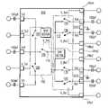
- FIG. 1is a set of schematic electrical circuit diagrams modeling the impedance of a conventional switch having two branches, two series switches per branch, with one branch in an “ON” state, according to the prior art;
- FIG. 2is a set of schematic electrical circuit diagrams modeling the impedance of a cascaded switch according to an embodiment of the invention, with the electrical switches of one selected branch being in an “ON” state;
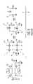
- FIG. 3is a set of schematic electrical circuit diagrams modeling the impedance of the circuit illustrated in FIG. 1 , with both branches being in an “OFF” state;
- FIG. 4is a set of schematic electrical circuit diagrams modeling the circuit shown in FIG. 2 , where both branches are in an “OFF” state;
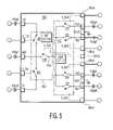
- FIG. 5is schematic electrical circuit diagram of a single-die integrated circuit for switching a plurality of transmitter and receiver ports to and from an antenna port according to one embodiment of the invention.
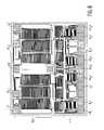
- FIG. 6is a plan view of a representative topological layout of the circuit illustrated in FIGS. 2 and 4 .
- FIGS. 1 and 2are sets of electrical schematic diagrams which model the impedance of a theoretical two-branch switching path according to conventional practice ( FIG. 1 ), and according to a cascaded method used in accordance with embodiments of the present invention ( FIG. 2 ).
- one branch 11 of illustrated switchis in an ON state, permitting a signal to pass from an input 12 to an output 14 .
- the other branch 15leads to an output 16 .
- Both topologiesare constructed of insulated gate field effect transistors (IGFETs).
- a two-branch switch indicated generally at 10has a first branch 11 which includes two FET switches 13 and 20 , here modeled as resistances with a value R.
- branch 15has two FETs 17 and 22 , which in their OFF state have dominating junction capacitances C.
- branch 11has an equivalent resistance 2R while branch 15 has an equivalent junction capacitance C/2. Simplifying by one more step, this is approximated by an overall insertion loss 21 of 2R.
- FIG. 2shows a switching schema having the same objective in which a signal propagates through the same number of switches or transistors as appear in the circuit in FIG. 1 .
- cascaded switch 23has a large capacity FET 19 with a gate perimeter that is twice that of e.g. FET 20 , therefore contributing an ON resistance of R/2.
- This FET 19takes the place of branch FETs 13 and 17 in FIG. 1 .
- ON FET 20exhibits a resistance R
- OFF FET 22shows a junction capacitance C.
- the first simplification of this circuitneglects the capacitance of FET 22 , leaving R/2 and R in series. As is shown in the last simplification, this reduces to an equivalent insertion loss of 3/2 R, which is less than the 2R insertion loss exhibited by the circuit of FIG. 1 .
- FIG. 3shows the conventional circuit of FIG. 1 but with both branches in an OFF state.
- the FETs 13 and 20 in branch 11each contribute a junction capacitance C, which reduces to C/2.
- the junction capacitance C of each of FETs 17 and 22 in branch 15combine to equivalent capacitance C/2.
- the impedance seen at input 12 of the OFF circuitis C.
- FIG. 4which is the circuit shown in FIG. 2 but with both branches OFF
- the junction capacitance contributed by large common switching FET 19is 2C.
- Branch FETs 20 and 22each show junction capacitance C. This reduces, as is shown in middle diagram 24 , to two capacitances in series each having a value of 2C.
- Simplified diagram 28shows that this reduces to an input impedance of C as seen from port 12 . In the OFF state, therefore, the conventional and cascaded methods yield the same impedance results.
- FIG. 5is a schematic layout of a cascaded-branch integrated circuit according to one embodiment of the invention.
- the present embodimentis fabricated on a single integrated circuit chip or die 100 .
- Chip 100has a plurality of signal and control ports/bonding pads at its outer margins.
- the transmitter portsare arranged along one side of the die, while the receiver ports are arranged along an opposite side of the die.
- the transmitter portsinclude ports Tx 2 and Tx 1 .
- the loads connected to these portsare modeled as 100 picofarad capacitors.
- Respectively associated with the transmitter ports Tx 1 and Tx 2are transmitter switching signal lines VTx 1 and VTx 2 .
- the left side of the diealso has an antenna port ANT to which one of the transmitter ports or one of the receiver ports is to be connected.
- the integrated circuit 100includes a single pole, three throw (SP3T) switching section 102 , the boundaries of which are shown in dotted and dashed line.
- SP3Tsingle pole, three throw
- Switching section 102includes a switch 104 which is operable by control line VTx 1 to connect transmitter port Tx 1 to the antenna port ANT.
- a similar switch 106is operable by switching signal VTx 2 to connect transmitter port Tx 2 to the antenna port ANT.
- a switch 108is a first stage in a cascaded switching system and is operable by a receiver switching signal VRxC to connect a receiver signal node 110 to the antenna port ANT. While, in the illustrated embodiment, the integrated circuit 100 selectively switches one of two transmitter ports, the invention also contemplates embodiments having one or three or more transmitter ports.
- the embodiment illustrated in FIG. 5has four receiver ports Rx 1 , Rx 2 , Rx 3 and Rx 4 , bonding pads for which are arranged along the right side (as seen in this Figure) of the die opposite the transmitter ports and the antenna port.
- a selected one of these receiver ports Rx 1 -Rx 4is switched by a single pole, four throw (SP4T) switching section 112 .
- the switching section 112is operable to switch one of four receiver ports Rx 1 -Rx 4 to the node 110 .
- the receiver switching section 112includes a switch 114 operable by control voltage VRx 4 to switch receiver port Rx 4 to the node 110 ; switch 116 operable by switching voltage VRx 3 to switch receiver port Rx 3 to node 110 ; switch 118 operable by switching voltage VRx 2 to switch receiver port Rx 2 to node 110 ; and switch 120 operable by switching voltage VRx 1 to switch receiver port Rx 1 to node 110 .
- One of the switches 114 - 120is operated in conjunction with switch 108 to connect a selected one of the receiver ports to the antenna port ANT.
- the receiver ports Rx 1 -Rx 4are modeled as including 100 picofarad external loads.
- the circuit 100switches one of two transmitter ports, or one of four receiver ports, to the antenna port, while isolating the rest.
- the number and kind of transmitter/receiver portscan be other than shown.
- a cascaded set of switcheswould be implemented for this, as is the case for the four receiver ports in this illustrated embodiment.
- a cascaded switching topologywould likewise be used on the receiver side where one of three or more receiver ports is to be switched to the antenna port.
- the number of receiver ports and/or the number of transmitter portscan be varied as desired, as the switching circuitry provided with each such port is largely modular.
- the multiple-series-FET switching elements 104 and 106are provided with the expectation that they will be switching signals of relatively high current to the antenna node for outbound, preferably wireless transmission.
- a signal sensed on the antennawill be weaker and therefore the switches 114 - 120 have a single FET each.
- the number and size of the switching transistorsmay be varied according to the contemplated strengths of the signals they are meant to switch.
- FIG. 6shows an exemplary layout and topography of an integrated switching circuit similar to that shown in FIG. 5 .
- the FETs for switching transmitter signals Tx 1 and Tx 2are shown at 102 , while the receiver switching section is shown at 112 .
- Each of the series switching FETsare high-power interdigitated switching transistors in which the sources and drains each have a plurality of fingers that are interleaved with each other.
- the interdigitated sources and drainsmay be created by suitable implants of a first conductivity type into a semiconductor substrate having an opposite conductivity type, and the implants may be self-aligned to the gates which are disposed between them.
- the gatesare sinuous metallizations, but in alternative embodiments the gates can be branched instead.
- the shapes of the channels of coursecorrespond to the gates.
- the second-stage receiver transistors in section 112are smaller, in recognition that they have to switch signals of less power.
- the transistorsare relatively small and in the illustrated embodiment have only one, noninterdigitated source and drain region apiece.
- the channels of the transistorsare doped so as to be depletion-mode devices.
- the resistorscan be created in a conventional manner, such as lines of polycrystalline silicon, and their values can be adjusted by adjusting their lengths.
- the integrated circuit in the illustrated embodimentcan operate in either of two transmission modes or any of four receiver modes. If, for example, a signal is to be transmitted from pad Tx 1 , VTx 1 will be high, and VTx 2 , VRxC, VRx 2 , VRx 1 , VRx 3 and VRx 4 will be low. This turns on series transistor topology 104 , and turns all other switching transistors off. In this condition the series transistor topology 104 will contribute a relatively low resistance to the insertion loss and the junction capacitance of the other, OFF branches of the circuit contribute little to the sensed impedance.
- control signals VTx 1 , VTx 2 , VRx 1 , VRx 2 and VRx 4will be low.
- Control signals VRx 3 and VRxCwill be high, turning on transistor topology 108 and transistor 116 .
- the ON transistors 108 , 116will contribute a relatively low amount of resistance to overall signal insertion loss; the relatively high junction capacitances contributed by the OFF branches are neglected. Hence, the cascaded circuit topology exhibits less signal insertion loss than the conventional noncascaded topology.
- FIGS. 5 and 6a single-die integrated circuit has been shown and described in FIGS. 5 and 6 which can be used to switch a plurality of wireless signals to and from an antenna.
- the described ICarranges its switching FETs in a cascaded topology, as is illustrated in FIGS. 2 and 4 , in order to reduce insertion loss in the strength of the switched signals.
- This reduced insertion loss resulting from the cascaded topologyenables a single die design in which receiver and transmission ports appear on the same die.
- prior art IC's that arrange their switching FETs using a conventional topology, as shown in FIGS. 1 and 3are required to provide receiver and transmission portions on separate dies, to avoid insertion loss and high capacitive loading.
- the integrated circuit in accordance with embodiments of the present inventionis useful for switching signals in CDMA, w-CDMA, IEEE 802.11, Bluetooth and like wireless protocols and saves space in comparison to chips which handle transmission or reception alone. While preferred embodiments of the present invention have been illustrated in the appended drawings and described in the detailed description above, the present invention is not limited thereto but only by the scope and spirit of the appended claims.
Landscapes
- Engineering & Computer Science (AREA)
- Computer Networks & Wireless Communication (AREA)
- Signal Processing (AREA)
- Electronic Switches (AREA)
- Junction Field-Effect Transistors (AREA)
Abstract
Description
Claims (16)
Priority Applications (6)
| Application Number | Priority Date | Filing Date | Title |
|---|---|---|---|
| US10/660,355US7869770B2 (en) | 2002-12-17 | 2003-09-11 | Apparatus, methods and articles of manufacture for a multi-band switch |
| US10/737,375US7515882B2 (en) | 2002-12-17 | 2003-12-16 | Apparatus, methods and articles of manufacture for a multi-band switch |
| PCT/US2003/040388WO2004059840A2 (en) | 2002-12-17 | 2003-12-17 | Apparatus, methods and articles of manufacture for a multiband switch |
| EP03814173AEP1573916A2 (en) | 2002-12-17 | 2003-12-17 | Apparatus, methods and articles of manufacture for a multiband switch |
| JP2005510009AJP2006511180A (en) | 2002-12-17 | 2003-12-17 | Manufacturing device, manufacturing method and product for multiband switch |
| AU2003301062AAU2003301062A1 (en) | 2002-12-17 | 2003-12-17 | Apparatus, methods and articles of manufacture for a multiband switch |
Applications Claiming Priority (2)
| Application Number | Priority Date | Filing Date | Title |
|---|---|---|---|
| US43438002P | 2002-12-17 | 2002-12-17 | |
| US10/660,355US7869770B2 (en) | 2002-12-17 | 2003-09-11 | Apparatus, methods and articles of manufacture for a multi-band switch |
Related Child Applications (1)
| Application Number | Title | Priority Date | Filing Date |
|---|---|---|---|
| US10/737,375Continuation-In-PartUS7515882B2 (en) | 2002-12-17 | 2003-12-16 | Apparatus, methods and articles of manufacture for a multi-band switch |
Publications (2)
| Publication Number | Publication Date |
|---|---|
| US20040113747A1 US20040113747A1 (en) | 2004-06-17 |
| US7869770B2true US7869770B2 (en) | 2011-01-11 |
Family
ID=32511749
Family Applications (1)
| Application Number | Title | Priority Date | Filing Date |
|---|---|---|---|
| US10/660,355Active2028-03-26US7869770B2 (en) | 2002-12-17 | 2003-09-11 | Apparatus, methods and articles of manufacture for a multi-band switch |
Country Status (5)
| Country | Link |
|---|---|
| US (1) | US7869770B2 (en) |
| EP (1) | EP1573916A2 (en) |
| JP (1) | JP2006511180A (en) |
| AU (1) | AU2003301062A1 (en) |
| WO (1) | WO2004059840A2 (en) |
Cited By (1)
| Publication number | Priority date | Publication date | Assignee | Title |
|---|---|---|---|---|
| US20130115895A1 (en)* | 2011-11-09 | 2013-05-09 | Skyworks Solutions, Inc. | Devices and methods related to field-effect transistor structures for radio-frequency applications |
Families Citing this family (5)
| Publication number | Priority date | Publication date | Assignee | Title |
|---|---|---|---|---|
| JP4202852B2 (en)* | 2003-08-27 | 2008-12-24 | 株式会社ルネサステクノロジ | Communication electronic parts and transmission / reception switching semiconductor device |
| US9172404B1 (en) | 2005-02-07 | 2015-10-27 | Rf Micro Devices, Inc. | Switch architecture for TDMA and FDD multiplexing |
| JP5108410B2 (en)* | 2007-07-31 | 2012-12-26 | サムソン エレクトロ−メカニックス カンパニーリミテッド. | Switch circuit |
| TWI385936B (en)* | 2007-11-21 | 2013-02-11 | Airoha Tech Corp | Wireless transceiver chip and its correction method |
| US10165516B2 (en)* | 2016-06-29 | 2018-12-25 | Silicon Laboratories Inc. | Systems and methods for switched protocol wireless connection |
Citations (19)
| Publication number | Priority date | Publication date | Assignee | Title |
|---|---|---|---|---|
| US4531235A (en) | 1983-06-20 | 1985-07-23 | Motorola, Inc. | Diversity signal strength indicator and site selection apparatus for using same |
| DE19832565A1 (en) | 1998-01-16 | 1999-08-05 | Mitsubishi Electric Corp | Transmitter-receiver selection switching module used in portable telephone |
| WO1999046859A1 (en) | 1998-03-11 | 1999-09-16 | Infineon Technologies Ag | Integrated circuit for mobile radio and mobile telephone installations |
| US6127886A (en)* | 1997-10-30 | 2000-10-03 | The Whitaker Corporation | Switched amplifying device |
| US6282186B1 (en) | 1998-02-19 | 2001-08-28 | Micron Technology, Inc. | Method of addressing messages and communications system |
| US6292060B1 (en)* | 1999-09-13 | 2001-09-18 | Chartered Semiconductor Manufacturing Ltd. | Technique to generate negative conductance in CMOS tuned cascode RF amplifiers |
| US6292047B1 (en)* | 1998-04-06 | 2001-09-18 | Motorola, Inc. | Switching down conversion mixer for use in multi-stage receiver architectures |
| US20010040479A1 (en)* | 2000-03-03 | 2001-11-15 | Shuyun Zhang | Electronic switch |
| US6324211B1 (en) | 1998-04-24 | 2001-11-27 | Micron Technology, Inc. | Interrogators communication systems communication methods and methods of processing a communication signal |
| US6366622B1 (en) | 1998-12-18 | 2002-04-02 | Silicon Wave, Inc. | Apparatus and method for wireless communications |
| US6396137B1 (en)* | 2000-03-15 | 2002-05-28 | Kevin Mark Klughart | Integrated voltage/current/power regulator/switch system and method |
| US6483391B1 (en) | 2001-03-30 | 2002-11-19 | Conexant Systems, Inc. | System for controlling the amplitude of an oscillator |
| US6492897B1 (en) | 2000-08-04 | 2002-12-10 | Richard A. Mowery, Jr. | System for coupling wireless signals to and from a power transmission line communication system |
| US6492192B1 (en) | 1996-05-13 | 2002-12-10 | Micron Technology, Inc. | Method of making a Schottky diode in an integrated circuit |
| US20030207668A1 (en)* | 2002-05-03 | 2003-11-06 | Mcfarland William J. | Dual frequency band wireless lan |
| US6671496B1 (en)* | 1999-09-02 | 2003-12-30 | Matsushita Electric Industrial Co., Ltd. | Transmitter and receiver communication apparatus with transmitter switch and receiver switch |
| US20040141470A1 (en)* | 2002-12-17 | 2004-07-22 | M/A Com, Inc. | Apparatus, methods and articles of manufacture for a multi-band switch |
| US20060118884A1 (en)* | 2004-11-05 | 2006-06-08 | Infineon Technologies Ag | High-frequency switching transistor and high-frequency circuit |
| US7269392B2 (en)* | 2003-08-27 | 2007-09-11 | Renesas Technology Corp. | Electric component for communication device and semiconductor device for switching transmission and reception |
- 2003
- 2003-09-11USUS10/660,355patent/US7869770B2/enactiveActive
- 2003-12-17EPEP03814173Apatent/EP1573916A2/ennot_activeWithdrawn
- 2003-12-17AUAU2003301062Apatent/AU2003301062A1/ennot_activeAbandoned
- 2003-12-17WOPCT/US2003/040388patent/WO2004059840A2/enactiveApplication Filing
- 2003-12-17JPJP2005510009Apatent/JP2006511180A/enactivePending
Patent Citations (22)
| Publication number | Priority date | Publication date | Assignee | Title |
|---|---|---|---|---|
| US4531235A (en) | 1983-06-20 | 1985-07-23 | Motorola, Inc. | Diversity signal strength indicator and site selection apparatus for using same |
| US6492192B1 (en) | 1996-05-13 | 2002-12-10 | Micron Technology, Inc. | Method of making a Schottky diode in an integrated circuit |
| US6351183B1 (en)* | 1997-10-30 | 2002-02-26 | The Whitaker Corporation | Switched amplifying device |
| US6127886A (en)* | 1997-10-30 | 2000-10-03 | The Whitaker Corporation | Switched amplifying device |
| US6066993A (en)* | 1998-01-16 | 2000-05-23 | Mitsubishi Denki Kabushiki Kaisha | Duplexer circuit apparatus provided with amplifier and impedance matching inductor |
| DE19832565A1 (en) | 1998-01-16 | 1999-08-05 | Mitsubishi Electric Corp | Transmitter-receiver selection switching module used in portable telephone |
| US6282186B1 (en) | 1998-02-19 | 2001-08-28 | Micron Technology, Inc. | Method of addressing messages and communications system |
| WO1999046859A1 (en) | 1998-03-11 | 1999-09-16 | Infineon Technologies Ag | Integrated circuit for mobile radio and mobile telephone installations |
| US6518855B1 (en)* | 1998-03-11 | 2003-02-11 | Infineon Technologies Ag | Integrated circuit for mobile radio and mobile telephone installations |
| US6292047B1 (en)* | 1998-04-06 | 2001-09-18 | Motorola, Inc. | Switching down conversion mixer for use in multi-stage receiver architectures |
| US6324211B1 (en) | 1998-04-24 | 2001-11-27 | Micron Technology, Inc. | Interrogators communication systems communication methods and methods of processing a communication signal |
| US6366622B1 (en) | 1998-12-18 | 2002-04-02 | Silicon Wave, Inc. | Apparatus and method for wireless communications |
| US6671496B1 (en)* | 1999-09-02 | 2003-12-30 | Matsushita Electric Industrial Co., Ltd. | Transmitter and receiver communication apparatus with transmitter switch and receiver switch |
| US6292060B1 (en)* | 1999-09-13 | 2001-09-18 | Chartered Semiconductor Manufacturing Ltd. | Technique to generate negative conductance in CMOS tuned cascode RF amplifiers |
| US20010040479A1 (en)* | 2000-03-03 | 2001-11-15 | Shuyun Zhang | Electronic switch |
| US6396137B1 (en)* | 2000-03-15 | 2002-05-28 | Kevin Mark Klughart | Integrated voltage/current/power regulator/switch system and method |
| US6492897B1 (en) | 2000-08-04 | 2002-12-10 | Richard A. Mowery, Jr. | System for coupling wireless signals to and from a power transmission line communication system |
| US6483391B1 (en) | 2001-03-30 | 2002-11-19 | Conexant Systems, Inc. | System for controlling the amplitude of an oscillator |
| US20030207668A1 (en)* | 2002-05-03 | 2003-11-06 | Mcfarland William J. | Dual frequency band wireless lan |
| US20040141470A1 (en)* | 2002-12-17 | 2004-07-22 | M/A Com, Inc. | Apparatus, methods and articles of manufacture for a multi-band switch |
| US7269392B2 (en)* | 2003-08-27 | 2007-09-11 | Renesas Technology Corp. | Electric component for communication device and semiconductor device for switching transmission and reception |
| US20060118884A1 (en)* | 2004-11-05 | 2006-06-08 | Infineon Technologies Ag | High-frequency switching transistor and high-frequency circuit |
Cited By (5)
| Publication number | Priority date | Publication date | Assignee | Title |
|---|---|---|---|---|
| US20130115895A1 (en)* | 2011-11-09 | 2013-05-09 | Skyworks Solutions, Inc. | Devices and methods related to field-effect transistor structures for radio-frequency applications |
| US20130130630A1 (en)* | 2011-11-09 | 2013-05-23 | Skyworks Solutions, Inc. | Radio-frequency switches having silicon-on-insulator field-effect transistors with reduced linear region resistance |
| US9064746B2 (en)* | 2011-11-09 | 2015-06-23 | Skyworks Solutions, Inc. | Devices and methods related to field-effect transistor structures for radio-frequency applications |
| US9159743B2 (en)* | 2011-11-09 | 2015-10-13 | Skyworks Solutions, Inc. | Radio-frequency switches having silicon-on-insulator field-effect transistors with reduced linear region resistance |
| US10014321B2 (en) | 2011-11-09 | 2018-07-03 | Skyworks Solutions, Inc. | Radio-frequency switches having silicon-on-insulator field-effect transistors with reduced linear region resistance |
Also Published As
| Publication number | Publication date |
|---|---|
| JP2006511180A (en) | 2006-03-30 |
| US20040113747A1 (en) | 2004-06-17 |
| EP1573916A2 (en) | 2005-09-14 |
| AU2003301062A1 (en) | 2004-07-22 |
| WO2004059840A3 (en) | 2004-11-18 |
| WO2004059840A2 (en) | 2004-07-15 |
Similar Documents
| Publication | Publication Date | Title |
|---|---|---|
| US7515882B2 (en) | Apparatus, methods and articles of manufacture for a multi-band switch | |
| EP3069446B1 (en) | Circuits and methods for improved quality factor in a stack of transistors | |
| US9866244B2 (en) | Electromagnetic couplers for multi-frequency power detection | |
| US9641201B2 (en) | System and method for a radio frequency integrated circuit | |
| JP4000103B2 (en) | High frequency switch device and high frequency switch structure | |
| KR102175613B1 (en) | Flexible l-network antenna tuner circuit | |
| US9941582B2 (en) | Switch module, front-end module, and driving method for switch module | |
| US7023272B2 (en) | Multi-band low noise amplifier system | |
| US10103696B1 (en) | Integrated gallium nitride power amplifier and switch | |
| US8451044B2 (en) | Switching circuit | |
| JP2019080080A (en) | Switching device, radio-frequency switching module, and electronic device | |
| US11190183B2 (en) | High throw-count RF switch | |
| JP2007129571A (en) | High frequency switch circuit and semiconductor device | |
| US7889023B2 (en) | Switching circuit for millimeter waveband control circuit | |
| US7337547B2 (en) | High frequency switching circuit device | |
| US7869770B2 (en) | Apparatus, methods and articles of manufacture for a multi-band switch | |
| KR101931682B1 (en) | SPDT switch structure including Transmission Line Transformer(TLT) for single antenna operation | |
| JP3798855B2 (en) | Signal selector switch | |
| CN100365932C (en) | Apparatus, method and article of manufacture for multiband switch | |
| JP4147827B2 (en) | High frequency switch circuit and communication device using the same | |
| US20240056056A1 (en) | Fine trimming of a radio frequency gain by modulating the periphery of a radio frequency switch | |
| Jung et al. | A CMOS single-pole-four-throw switch | |
| WO2023086789A1 (en) | Hybrid input lna rf frontend architecture | |
| JP2002026268A (en) | Ic switch | |
| JP2005005857A (en) | Switch circuit apparatus |
Legal Events
| Date | Code | Title | Description |
|---|---|---|---|
| AS | Assignment | Owner name:M/A-COM, INC., MASSACHUSETTS Free format text:ASSIGNMENT OF ASSIGNORS INTEREST;ASSIGNOR:KELCOURSE, MARK F.;REEL/FRAME:014498/0814 Effective date:20030910 | |
| AS | Assignment | Owner name:COBHAM DEFENSE ELECTRONIC SYSTEMS CORPORATION, MAS Free format text:ASSIGNMENT OF ASSIGNORS INTEREST;ASSIGNORS:M/A COM, INC.;RAYCHEM INTERNATIONAL;TYCO ELECTRONICS CORPORATION;AND OTHERS;REEL/FRAME:022266/0400;SIGNING DATES FROM 20080108 TO 20090113 Owner name:COBHAM DEFENSE ELECTRONIC SYSTEMS CORPORATION,MASS Free format text:ASSIGNMENT OF ASSIGNORS INTEREST;ASSIGNORS:M/A COM, INC.;RAYCHEM INTERNATIONAL;TYCO ELECTRONICS CORPORATION;AND OTHERS;SIGNING DATES FROM 20080108 TO 20090113;REEL/FRAME:022266/0400 Owner name:COBHAM DEFENSE ELECTRONIC SYSTEMS CORPORATION, MAS Free format text:ASSIGNMENT OF ASSIGNORS INTEREST;ASSIGNORS:M/A COM, INC.;RAYCHEM INTERNATIONAL;TYCO ELECTRONICS CORPORATION;AND OTHERS;SIGNING DATES FROM 20080108 TO 20090113;REEL/FRAME:022266/0400 | |
| AS | Assignment | Owner name:COBHAM DEFENSE ELECTRONIC SYSTEMS CORPORATION, MAS Free format text:SECURITY AGREEMENT;ASSIGNOR:KIWI STONE ACQUISITION CORP.;REEL/FRAME:022482/0016 Effective date:20090330 Owner name:COBHAM DEFENSE ELECTRONIC SYSTEMS CORPORATION,MASS Free format text:SECURITY AGREEMENT;ASSIGNOR:KIWI STONE ACQUISITION CORP.;REEL/FRAME:022482/0016 Effective date:20090330 | |
| AS | Assignment | Owner name:KIWI STONE ACQUISITION CORPORATION, CALIFORNIA Free format text:ASSIGNMENT OF ASSIGNORS INTEREST;ASSIGNOR:COBHAM DEFENSE ELECTRONIC SYSTEMS CORPORATION;REEL/FRAME:022714/0890 Effective date:20090521 Owner name:KIWI STONE ACQUISITION CORPORATION,CALIFORNIA Free format text:ASSIGNMENT OF ASSIGNORS INTEREST;ASSIGNOR:COBHAM DEFENSE ELECTRONIC SYSTEMS CORPORATION;REEL/FRAME:022714/0890 Effective date:20090521 | |
| AS | Assignment | Owner name:M/A-COM TECHNOLOGY SOLUTIONS HOLDINGS, INC., MASSA Free format text:CHANGE OF NAME;ASSIGNOR:KIWI STONE ACQUISITION CORP.;REEL/FRAME:023476/0069 Effective date:20090526 Owner name:M/A-COM TECHNOLOGY SOLUTIONS HOLDINGS, INC.,MASSAC Free format text:CHANGE OF NAME;ASSIGNOR:KIWI STONE ACQUISITION CORP.;REEL/FRAME:023476/0069 Effective date:20090526 | |
| AS | Assignment | Owner name:RBS BUSINESS CAPITAL, A DIVISION OF RBS ASSET FINA Free format text:SECURITY AGREEMENT;ASSIGNORS:MIMIX BROADBAND, INC.;M/A-COM TECHNOLOGY SOLUTIONS HOLDINGS, INC.;REEL/FRAME:025444/0920 Effective date:20101203 | |
| AS | Assignment | Owner name:M/A-COM TECHNOLOGY SOLUTIONS HOLDINGS, INC., MASSA Free format text:RELEASE BY SECURED PARTY;ASSIGNOR:COBHAM DEFENSE ELECTRONIC SYSTEMS CORPORATION;REEL/FRAME:025445/0947 Effective date:20101203 | |
| STCF | Information on status: patent grant | Free format text:PATENTED CASE | |
| AS | Assignment | Owner name:JPMORGAN CHASE BANK, N.A., AS ADMINISTRATIVE AGENT Free format text:SECURITY AGREEMENT;ASSIGNOR:M/A-COM TECHNOLOGY SOLUTIONS HOLDINGS, INC.;REEL/FRAME:027015/0444 Effective date:20110930 | |
| AS | Assignment | Owner name:M/A-COM TECHNOLOGY SOLUTIONS HOLDINGS, INC., MASSA Free format text:RELEASE OF SECURITY INTEREST RECORDED AT REEL/FRAME 25444/920;ASSIGNOR:RBS BUSINESS CAPITAL, A DIVISION OF RBS ASSET FINANCE, INC., AS ADMINISTRATIVE AGENT;REEL/FRAME:027028/0021 Effective date:20110930 Owner name:MIMIX BROADBAND, INC., MASSACHUSETTS Free format text:RELEASE OF SECURITY INTEREST RECORDED AT REEL/FRAME 25444/920;ASSIGNOR:RBS BUSINESS CAPITAL, A DIVISION OF RBS ASSET FINANCE, INC., AS ADMINISTRATIVE AGENT;REEL/FRAME:027028/0021 Effective date:20110930 | |
| AS | Assignment | Owner name:JPMORGAN CHASE BANK, N.A., AS ADMINISTRATIVE AGENT Free format text:SECURITY AGREEMENT;ASSIGNOR:M/A-COM TECHNOLOGY SOLUTIONS HOLDINGS, INC.;REEL/FRAME:031314/0183 Effective date:20130926 | |
| FEPP | Fee payment procedure | Free format text:PAYOR NUMBER ASSIGNED (ORIGINAL EVENT CODE: ASPN); ENTITY STATUS OF PATENT OWNER: LARGE ENTITY | |
| AS | Assignment | Owner name:M/A-COM TECHNOLOGY SOLUTIONS HOLDINGS, INC., MASSA Free format text:RELEASE BY SECURED PARTY;ASSIGNOR:JPMORGAN CHASE BANK, N.A.;REEL/FRAME:032857/0032 Effective date:20140508 | |
| AS | Assignment | Owner name:GOLDMAN SACHS BANK USA, NEW YORK Free format text:SECURITY INTEREST;ASSIGNORS:M/A-COM TECHNOLOGY SOLUTIONS HOLDINGS, INC.;MINDSPEED TECHNOLOGIES, INC.;BROOKTREE CORPORATION;REEL/FRAME:032859/0374 Effective date:20140508 | |
| FPAY | Fee payment | Year of fee payment:4 | |
| AS | Assignment | Owner name:MACOM TECHNOLOGY SOLUTIONS HOLDINGS, INC., MASSACH Free format text:CHANGE OF NAME;ASSIGNOR:M/A-COM TECHNOLOGY SOLUTIONS HOLDINGS, INC.;REEL/FRAME:039139/0826 Effective date:20160601 | |
| MAFP | Maintenance fee payment | Free format text:PAYMENT OF MAINTENANCE FEE, 8TH YEAR, LARGE ENTITY (ORIGINAL EVENT CODE: M1552) Year of fee payment:8 | |
| MAFP | Maintenance fee payment | Free format text:PAYMENT OF MAINTENANCE FEE, 12TH YEAR, LARGE ENTITY (ORIGINAL EVENT CODE: M1553); ENTITY STATUS OF PATENT OWNER: LARGE ENTITY Year of fee payment:12 |