US7869186B2 - High Q and low stress capacitor electrode array - Google Patents
High Q and low stress capacitor electrode arrayDownload PDFInfo
- Publication number
- US7869186B2 US7869186B2US11/598,354US59835406AUS7869186B2US 7869186 B2US7869186 B2US 7869186B2US 59835406 AUS59835406 AUS 59835406AUS 7869186 B2US7869186 B2US 7869186B2
- Authority
- US
- United States
- Prior art keywords
- electrode
- capacitor
- subsections
- tunable dielectric
- broken
- Prior art date
- Legal status (The legal status is an assumption and is not a legal conclusion. Google has not performed a legal analysis and makes no representation as to the accuracy of the status listed.)
- Active, expires
Links
- 239000003990capacitorSubstances0.000titleclaimsabstractdescription67
- 239000007787solidSubstances0.000claimsabstractdescription23
- 239000003989dielectric materialSubstances0.000claimsdescription20
- 229910052751metalInorganic materials0.000claimsdescription18
- 239000002184metalSubstances0.000claimsdescription18
- 150000002739metalsChemical class0.000claimsdescription14
- 230000009467reductionEffects0.000claimsdescription5
- 230000008859changeEffects0.000claimsdescription4
- 229910003460diamondInorganic materials0.000claimsdescription3
- 239000010432diamondSubstances0.000claimsdescription3
- 229910044991metal oxideInorganic materials0.000description15
- 150000004706metal oxidesChemical class0.000description15
- 239000000463materialSubstances0.000description14
- 239000002131composite materialSubstances0.000description12
- -1BaCaZrTiO3Inorganic materials0.000description11
- 239000000395magnesium oxideSubstances0.000description11
- CPLXHLVBOLITMK-UHFFFAOYSA-Nmagnesium oxideInorganic materials[Mg]=OCPLXHLVBOLITMK-UHFFFAOYSA-N0.000description11
- 229910052454barium strontium titanateInorganic materials0.000description10
- AXZKOIWUVFPNLO-UHFFFAOYSA-Nmagnesium;oxygen(2-)Chemical compound[O-2].[Mg+2]AXZKOIWUVFPNLO-UHFFFAOYSA-N0.000description10
- 238000000034methodMethods0.000description10
- 229910052914metal silicateInorganic materials0.000description9
- 229910052839forsteriteInorganic materials0.000description8
- 239000011777magnesiumSubstances0.000description8
- 239000011575calciumSubstances0.000description6
- 239000000919ceramicSubstances0.000description6
- 229910002971CaTiO3Inorganic materials0.000description5
- 229910017676MgTiO3Inorganic materials0.000description5
- 229910052791calciumInorganic materials0.000description5
- 239000010408filmSubstances0.000description5
- 229910052744lithiumInorganic materials0.000description5
- 229910052749magnesiumInorganic materials0.000description5
- 239000000203mixtureSubstances0.000description5
- VYPSYNLAJGMNEJ-UHFFFAOYSA-NSilicium dioxideChemical compoundO=[Si]=OVYPSYNLAJGMNEJ-UHFFFAOYSA-N0.000description4
- 239000000654additiveSubstances0.000description4
- 229910052788bariumInorganic materials0.000description4
- WMWLMWRWZQELOS-UHFFFAOYSA-Nbismuth(iii) oxideChemical compoundO=[Bi]O[Bi]=OWMWLMWRWZQELOS-UHFFFAOYSA-N0.000description4
- 150000001875compoundsChemical class0.000description4
- TWNQGVIAIRXVLR-UHFFFAOYSA-Noxo(oxoalumanyloxy)alumaneChemical compoundO=[Al]O[Al]=OTWNQGVIAIRXVLR-UHFFFAOYSA-N0.000description4
- 230000000737periodic effectEffects0.000description4
- 229910052700potassiumInorganic materials0.000description4
- 229910052708sodiumInorganic materials0.000description4
- 239000011734sodiumSubstances0.000description4
- 229910052712strontiumInorganic materials0.000description4
- 229910052882wollastoniteInorganic materials0.000description4
- 229910026161MgAl2O4Inorganic materials0.000description3
- 229910003383SrSiO3Inorganic materials0.000description3
- 239000003985ceramic capacitorSubstances0.000description3
- 229910052748manganeseInorganic materials0.000description3
- 239000011572manganeseSubstances0.000description3
- 238000004519manufacturing processMethods0.000description3
- 150000004760silicatesChemical class0.000description3
- 229910052596spinelInorganic materials0.000description3
- 239000010409thin filmSubstances0.000description3
- 229910015846BaxSr1-xTiO3Inorganic materials0.000description2
- 229910004774CaSnO3Inorganic materials0.000description2
- 229910002976CaZrO3Inorganic materials0.000description2
- PWHULOQIROXLJO-UHFFFAOYSA-NManganeseChemical compound[Mn]PWHULOQIROXLJO-UHFFFAOYSA-N0.000description2
- 229910002370SrTiO3Inorganic materials0.000description2
- 229910010252TiO3Inorganic materials0.000description2
- 150000004645aluminatesChemical class0.000description2
- 229910052782aluminiumInorganic materials0.000description2
- 230000008901benefitEffects0.000description2
- 229910052790berylliumInorganic materials0.000description2
- 229910052792caesiumInorganic materials0.000description2
- 229910010293ceramic materialInorganic materials0.000description2
- 229910052681coesiteInorganic materials0.000description2
- 239000000470constituentSubstances0.000description2
- 229910052906cristobaliteInorganic materials0.000description2
- 229910052730franciumInorganic materials0.000description2
- NUJOXMJBOLGQSY-UHFFFAOYSA-Nmanganese dioxideChemical compoundO=[Mn]=ONUJOXMJBOLGQSY-UHFFFAOYSA-N0.000description2
- RVTZCBVAJQQJTK-UHFFFAOYSA-Noxygen(2-);zirconium(4+)Chemical compound[O-2].[O-2].[Zr+4]RVTZCBVAJQQJTK-UHFFFAOYSA-N0.000description2
- 230000003071parasitic effectEffects0.000description2
- 229910052705radiumInorganic materials0.000description2
- 229910001404rare earth metal oxideInorganic materials0.000description2
- 229910052701rubidiumInorganic materials0.000description2
- 229910052710siliconInorganic materials0.000description2
- 239000000377silicon dioxideSubstances0.000description2
- VWDWKYIASSYTQR-UHFFFAOYSA-Nsodium nitrateChemical compound[Na+].[O-][N+]([O-])=OVWDWKYIASSYTQR-UHFFFAOYSA-N0.000description2
- 229910052682stishoviteInorganic materials0.000description2
- 229910052719titaniumInorganic materials0.000description2
- 229910052905tridymiteInorganic materials0.000description2
- 229910052721tungstenInorganic materials0.000description2
- 229910052726zirconiumInorganic materials0.000description2
- 229910001928zirconium oxideInorganic materials0.000description2
- 229910002929BaSnO3Inorganic materials0.000description1
- 229910004829CaWO4Inorganic materials0.000description1
- 229910052684CeriumInorganic materials0.000description1
- XEEYBQQBJWHFJM-UHFFFAOYSA-NIronChemical compound[Fe]XEEYBQQBJWHFJM-UHFFFAOYSA-N0.000description1
- 229910003334KNbO3Inorganic materials0.000description1
- 229910007562Li2SiO3Inorganic materials0.000description1
- 229910003327LiNbO3Inorganic materials0.000description1
- 229910012463LiTaO3Inorganic materials0.000description1
- WHXSMMKQMYFTQS-UHFFFAOYSA-NLithiumChemical compound[Li]WHXSMMKQMYFTQS-UHFFFAOYSA-N0.000description1
- 229910052779NeodymiumInorganic materials0.000description1
- 229910003781PbTiO3Inorganic materials0.000description1
- 229910052777PraseodymiumInorganic materials0.000description1
- 239000004115Sodium SilicateSubstances0.000description1
- 229910004481Ta2O3Inorganic materials0.000description1
- 229920002253TannatePolymers0.000description1
- RTAQQCXQSZGOHL-UHFFFAOYSA-NTitaniumChemical compound[Ti]RTAQQCXQSZGOHL-UHFFFAOYSA-N0.000description1
- MCMNRKCIXSYSNV-UHFFFAOYSA-NZrO2Inorganic materialsO=[Zr]=OMCMNRKCIXSYSNV-UHFFFAOYSA-N0.000description1
- AZJLMWQBMKNUKB-UHFFFAOYSA-N[Zr].[La]Chemical compound[Zr].[La]AZJLMWQBMKNUKB-UHFFFAOYSA-N0.000description1
- 230000000996additive effectEffects0.000description1
- 229910052656albiteInorganic materials0.000description1
- 229910000287alkaline earth metal oxideInorganic materials0.000description1
- 229910052661anorthiteInorganic materials0.000description1
- 229910021523barium zirconateInorganic materials0.000description1
- 229910052797bismuthInorganic materials0.000description1
- BRPQOXSCLDDYGP-UHFFFAOYSA-Ncalcium oxideChemical compound[O-2].[Ca+2]BRPQOXSCLDDYGP-UHFFFAOYSA-N0.000description1
- 239000000292calcium oxideSubstances0.000description1
- ODINCKMPIJJUCX-UHFFFAOYSA-Ncalcium oxideInorganic materials[Ca]=OODINCKMPIJJUCX-UHFFFAOYSA-N0.000description1
- 229910052804chromiumInorganic materials0.000description1
- 229910052637diopsideInorganic materials0.000description1
- 230000000694effectsEffects0.000description1
- 230000005684electric fieldEffects0.000description1
- 229910000174eucryptiteInorganic materials0.000description1
- 230000002349favourable effectEffects0.000description1
- 239000011521glassSubstances0.000description1
- 229910052735hafniumInorganic materials0.000description1
- JYTUFVYWTIKZGR-UHFFFAOYSA-Nholmium oxideInorganic materials[O][Ho]O[Ho][O]JYTUFVYWTIKZGR-UHFFFAOYSA-N0.000description1
- 229910052909inorganic silicateInorganic materials0.000description1
- 229910052746lanthanumInorganic materials0.000description1
- MRELNEQAGSRDBK-UHFFFAOYSA-Nlanthanum oxideInorganic materials[O-2].[O-2].[O-2].[La+3].[La+3]MRELNEQAGSRDBK-UHFFFAOYSA-N0.000description1
- 229910052745leadInorganic materials0.000description1
- HTUMBQDCCIXGCV-UHFFFAOYSA-Nlead oxideChemical compound[O-2].[Pb+2]HTUMBQDCCIXGCV-UHFFFAOYSA-N0.000description1
- YEXPOXQUZXUXJW-UHFFFAOYSA-Nlead(II) oxideInorganic materials[Pb]=OYEXPOXQUZXUXJW-UHFFFAOYSA-N0.000description1
- 238000012986modificationMethods0.000description1
- 230000004048modificationEffects0.000description1
- 229910052750molybdenumInorganic materials0.000description1
- PLDDOISOJJCEMH-UHFFFAOYSA-Nneodymium oxideInorganic materials[O-2].[O-2].[O-2].[Nd+3].[Nd+3]PLDDOISOJJCEMH-UHFFFAOYSA-N0.000description1
- 229910052758niobiumInorganic materials0.000description1
- KTUFCUMIWABKDW-UHFFFAOYSA-Noxo(oxolanthaniooxy)lanthanumChemical compoundO=[La]O[La]=OKTUFCUMIWABKDW-UHFFFAOYSA-N0.000description1
- 229910052761rare earth metalInorganic materials0.000description1
- 150000002910rare earth metalsChemical class0.000description1
- 239000003870refractory metalSubstances0.000description1
- 229910052706scandiumInorganic materials0.000description1
- 229910052911sodium silicateInorganic materials0.000description1
- 235000019351sodium silicatesNutrition0.000description1
- 125000005402stannate groupChemical group0.000description1
- 229910014031strontium zirconium oxideInorganic materials0.000description1
- 229910052715tantalumInorganic materials0.000description1
- 229910052718tinInorganic materials0.000description1
- 229910052723transition metalInorganic materials0.000description1
- 229910000314transition metal oxideInorganic materials0.000description1
- 150000003624transition metalsChemical class0.000description1
- WFKWXMTUELFFGS-UHFFFAOYSA-NtungstenChemical compound[W]WFKWXMTUELFFGS-UHFFFAOYSA-N0.000description1
- 239000010937tungstenSubstances0.000description1
- 229910052720vanadiumInorganic materials0.000description1
- 229910052844willemiteInorganic materials0.000description1
- FIXNOXLJNSSSLJ-UHFFFAOYSA-Nytterbium(III) oxideInorganic materialsO=[Yb]O[Yb]=OFIXNOXLJNSSSLJ-UHFFFAOYSA-N0.000description1
- 229910052727yttriumInorganic materials0.000description1
- 229910052845zirconInorganic materials0.000description1
Images

Classifications
- H—ELECTRICITY
- H01—ELECTRIC ELEMENTS
- H01G—CAPACITORS; CAPACITORS, RECTIFIERS, DETECTORS, SWITCHING DEVICES, LIGHT-SENSITIVE OR TEMPERATURE-SENSITIVE DEVICES OF THE ELECTROLYTIC TYPE
- H01G4/00—Fixed capacitors; Processes of their manufacture
- H01G4/002—Details
- H01G4/228—Terminals
- H—ELECTRICITY
- H01—ELECTRIC ELEMENTS
- H01G—CAPACITORS; CAPACITORS, RECTIFIERS, DETECTORS, SWITCHING DEVICES, LIGHT-SENSITIVE OR TEMPERATURE-SENSITIVE DEVICES OF THE ELECTROLYTIC TYPE
- H01G4/00—Fixed capacitors; Processes of their manufacture
- H01G4/38—Multiple capacitors, i.e. structural combinations of fixed capacitors
- H—ELECTRICITY
- H01—ELECTRIC ELEMENTS
- H01G—CAPACITORS; CAPACITORS, RECTIFIERS, DETECTORS, SWITCHING DEVICES, LIGHT-SENSITIVE OR TEMPERATURE-SENSITIVE DEVICES OF THE ELECTROLYTIC TYPE
- H01G7/00—Capacitors in which the capacitance is varied by non-mechanical means; Processes of their manufacture
- H01G7/06—Capacitors in which the capacitance is varied by non-mechanical means; Processes of their manufacture having a dielectric selected for the variation of its permittivity with applied voltage, i.e. ferroelectric capacitors
- H—ELECTRICITY
- H01—ELECTRIC ELEMENTS
- H01L—SEMICONDUCTOR DEVICES NOT COVERED BY CLASS H10
- H01L23/00—Details of semiconductor or other solid state devices
- H01L23/52—Arrangements for conducting electric current within the device in operation from one component to another, i.e. interconnections, e.g. wires, lead frames
- H01L23/522—Arrangements for conducting electric current within the device in operation from one component to another, i.e. interconnections, e.g. wires, lead frames including external interconnections consisting of a multilayer structure of conductive and insulating layers inseparably formed on the semiconductor body
- H01L23/5222—Capacitive arrangements or effects of, or between wiring layers
- H01L23/5223—Capacitor integral with wiring layers
- H—ELECTRICITY
- H01—ELECTRIC ELEMENTS
- H01L—SEMICONDUCTOR DEVICES NOT COVERED BY CLASS H10
- H01L2924/00—Indexing scheme for arrangements or methods for connecting or disconnecting semiconductor or solid-state bodies as covered by H01L24/00
- H01L2924/0001—Technical content checked by a classifier
- H01L2924/0002—Not covered by any one of groups H01L24/00, H01L24/00 and H01L2224/00
- H—ELECTRICITY
- H10—SEMICONDUCTOR DEVICES; ELECTRIC SOLID-STATE DEVICES NOT OTHERWISE PROVIDED FOR
- H10D—INORGANIC ELECTRIC SEMICONDUCTOR DEVICES
- H10D1/00—Resistors, capacitors or inductors
- H10D1/01—Manufacture or treatment
- H10D1/041—Manufacture or treatment of capacitors having no potential barriers
- H10D1/042—Manufacture or treatment of capacitors having no potential barriers using deposition processes to form electrode extensions
- H—ELECTRICITY
- H10—SEMICONDUCTOR DEVICES; ELECTRIC SOLID-STATE DEVICES NOT OTHERWISE PROVIDED FOR
- H10D—INORGANIC ELECTRIC SEMICONDUCTOR DEVICES
- H10D1/00—Resistors, capacitors or inductors
- H10D1/60—Capacitors
- H10D1/68—Capacitors having no potential barriers
- H10D1/692—Electrodes
- H10D1/711—Electrodes having non-planar surfaces, e.g. formed by texturisation
- H10D1/714—Electrodes having non-planar surfaces, e.g. formed by texturisation having horizontal extensions
- Y—GENERAL TAGGING OF NEW TECHNOLOGICAL DEVELOPMENTS; GENERAL TAGGING OF CROSS-SECTIONAL TECHNOLOGIES SPANNING OVER SEVERAL SECTIONS OF THE IPC; TECHNICAL SUBJECTS COVERED BY FORMER USPC CROSS-REFERENCE ART COLLECTIONS [XRACs] AND DIGESTS
- Y10—TECHNICAL SUBJECTS COVERED BY FORMER USPC
- Y10T—TECHNICAL SUBJECTS COVERED BY FORMER US CLASSIFICATION
- Y10T29/00—Metal working
- Y10T29/43—Electric condenser making
- Y10T29/435—Solid dielectric type
- Y—GENERAL TAGGING OF NEW TECHNOLOGICAL DEVELOPMENTS; GENERAL TAGGING OF CROSS-SECTIONAL TECHNOLOGIES SPANNING OVER SEVERAL SECTIONS OF THE IPC; TECHNICAL SUBJECTS COVERED BY FORMER USPC CROSS-REFERENCE ART COLLECTIONS [XRACs] AND DIGESTS
- Y10—TECHNICAL SUBJECTS COVERED BY FORMER USPC
- Y10T—TECHNICAL SUBJECTS COVERED BY FORMER US CLASSIFICATION
- Y10T29/00—Metal working
- Y10T29/49—Method of mechanical manufacture
- Y10T29/49002—Electrical device making
- Y10T29/49005—Acoustic transducer
Definitions
- ESRError-to-Resistance
- the ESRvaries with frequency for a given capacitor, and is “equivalent” because its source is from the characteristics of the conducting electrode structures and in the insulating dielectric structure.
- the ESRis represented as a single series parasitic element.
- all capacitor parameterswere measured at a standard of 1 MHz, but in today's high frequency world, this is far from sufficient.
- Typical values for a good high frequency capacitor of a given valuecould run in the order of about 0.05 ohms at 200 MHz, 0.11 ohms at 900 MHz, and 0.14 ohms at 2000 MHz.
- the quality factor Qis a dimensionless number that is equal to the capacitor's reactance divided by the capacitor's parasitic resistance (ESR).
- ESRparasitic resistance
- An embodiment of the present inventionprovides a capacitor, comprising a solid electrode, an electrode broken into subsections with a signal bus lines connecting the subsections; and wherein the signal bus further connects the solid electrode with the electrode broken into subsections.
- the capacitor of an embodiment of the present inventionmay further comprise a voltage tunable dielectric material between the solid electrode and the electrode broken into subsections to enable the capacitor to be voltage tunable.
- the broken electrodemay distribute the signal across the capacitor area and increase the effective width of a signal path through the solid electrode.
- the capacitormay be a planar integrated capacitors or a discrete ceramic capacitor and the capacitor may be a pair of series capacitors and wherein the subsections are arranged in such a manner that it increases the effective width of the signal path in the solid electrode.
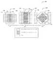
- FIG. 1illustrates three, of many possible, capacitor electrode structures of some embodiments of the present invention.
- FIG. 2illustrates a method of one embodiment of the present invention.
- Coupledmay be used to indicate that two or more elements are in direct physical or electrical contact with each other.
- Connectedmay be used to indicate that two or more elements are in direct physical or electrical contact with each other.
- Connectedmay be used to indicate that two or more elements are in either direct or indirect (with other intervening elements between them) physical or electrical contact with each other, and/or that the two or more elements co-operate or interact with each other (e.g. as in a cause an effect relationship).
- An embodiment of the present inventionprovides a capacitor electrode structure that allows for the creation of very high “Q” (low resistance) capacitors. It is particularly well suited to common capacitor material structures wherein one electrode is made from a higher resistance metal than the opposite electrode. Examples of capacitors with such material properties can be found in planar integrated capacitors, as well as discrete ceramic capacitors.
- the structure of an embodiment of the present inventionalso reduces the mechanical stresses generated in the metals and dielectric films of the capacitor.
- the inventionincludes electrodes broken into subsections, signal bus lines to connect the subsections, and a solid electrode. The broken electrode should have the lower resistance of the two. The broken electrode may distribute the signal across the capacitor area and, through proper arrangement, increase the effective width of the signal path through the higher resistance solid electrode.
- the present electrodesmay include a voltage tunable dielectric material 137 between the electrodes and the voltage tunable dielectric material may be a Parascan® voltage tunable dielectric material.
- This structurerealizes these benefits by breaking two of the electrodes of a pair of series capacitors into subsections.
- the sectionsare arranged in such a manner that it increases the effective width of the signal path in the higher resistance electrode. These subsections are then electrically connected through signal bus line. The reduction in stress occurs because the individual electrode subsections retain and create less stress than a single plate of similar area.
- FIG. 1shown generally as 100 are images of two series capacitors.
- the left most, FIG. 1A , design 110is fairly standard with solid high resistance electrode 120 and low resistance electrodes 122 connected by signal bus lines 115 .
- two exemplary embodiments of the present inventionare shown in the center 125 and on the right 140 .
- Center capacitor, FIG. 1B 125may include solid high resistance electrode 135 and low resistance electrodes 132 connected by bus 130 .
- Right capacitor, FIG. 1C 140may include solid high resistance electrode 150 and low resistance electrodes 155 connected by signal bus lines 145 .
- the reduction in resistance, leading to an increase in Qoccurs because the length of the signal path stays the same while the effective width increases. For example, breaking the electrode as shown in the middle image 125 increases the width to 3.5 times that of the conventional capacitor.
- the rightmost “diamond” configuration 140increases that width to 4.25 times that of the conventional.
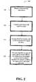
- FIG. 2generally at 200 , is provided a method according to one embodiment of the present invention which may comprise breaking an electrode into subsections 205 with signal bus lines connecting said subsections 210 and a solid electrode 215 to improve Q.
- the methodmay further comprise distributing the signal across said capacitor area by said broken electrode and thereby increasing the effective width of a signal path through said solid electrode.
- the capacitormay be a planar integrated capacitor or a discrete ceramic capacitor in the method of an embodiment of the present invention.
- the methodmay still further comprise adapting said solid electrode and said broken electrode to reduce the mechanical stresses generated in the metals and dielectric films of said capacitor and as shown at 220 using said capacitor in a pair of series capacitors and wherein said subsections are arranged in such a manner that it increases the effective width of the signal path in said solid electrode.
- the at least one voltage tunable dielectric capacitormay be a series network of voltage tunable dielectric capacitors which are all tuned using a common tuning voltage.
- BSTmay be used as a tunable dielectric material that may be used in a tunable dielectric capacitor of the present invention.
- Paratek Microwave, Inc.has developed and continues to develop tunable dielectric materials that may be utilized in embodiments of the present invention and thus the present invention is not limited to using BST material.
- This family of tunable dielectric materialsmay be referred to as Parascan®.
- Parascan®as used herein is a trademarked term indicating a tunable dielectric material developed by the assignee of the present invention.
- Parascan® tunable dielectric materialshave been described in several patents.
- Barium strontium titanate(BaTiO3-SrTiO3), also referred to as BSTO, is used for its high dielectric constant (200-6,000) and large change in dielectric constant with applied voltage (25-75 percent with a field of 2 Volts/micron).
- Tunable dielectric materials including barium strontium titanateare disclosed in U.S. Pat. No. 5,312,790 to Sengupta, et al. entitled “Ceramic Ferroelectric Material”; U.S. Pat. No.
- Barium strontium titanate of the formula Ba x Sr 1-x TiO 3is a preferred electronically tunable dielectric material due to its favorable tuning characteristics, low Curie temperatures and low microwave loss properties.
- xcan be any value from 0 to 1, preferably from about 0.15 to about 0.6. More preferably, x is from 0.3 to 0.6.
- Other electronically tunable dielectric materialsmay be used partially or entirely in place of barium strontium titanate.
- An exampleis Ba x Ca 1-x TiO 3 , where x is in a range from about 0.2 to about 0.8, preferably from about 0.4 to about 0.6.
- Additional electronically tunable ferroelectricsinclude Pb x Zr 1-x TiO 3 (PZT) where x ranges from about 0.0 to about 1.0, Pb x Zr 1-x SrTiO 3 where x ranges from about 0.05 to about 0.4, KTa x Nb 1-x O 3 where x ranges from about 0.0 to about 1.0, lead lanthanum zirconium titanate (PLZT), PbTiO 3 , BaCaZrTiO 3 , NaNO 3 , KNbO 3 , LiNbO 3 , LiTaO 3 , PbNb 2 O 6 , PbTa 2 O 6 , KSr(NbO 3 ) and NaBa 2 (NbO 3 )5KH 2 PO 4 , and mixtures and compositions thereof.
- PZTPb x Zr 1-x TiO 3
- Pb x Zr 1-x SrTiO 3where x ranges from about 0.05 to about
- these materialscan be combined with low loss dielectric materials, such as magnesium oxide (MgO), aluminum oxide (Al 2 O 3 ), and zirconium oxide (ZrO 2 ), and/or with additional doping elements, such as manganese (MN), iron (Fe), and tungsten (W), or with other alkali earth metal oxides (i.e. calcium oxide, etc.), transition metal oxides, silicates, niobates, tantalates, aluminates, zirconnates, and titanates to further reduce the dielectric loss.
- MgOmagnesium oxide
- Al 2 O 3aluminum oxide
- ZrO 2zirconium oxide
- additional doping elementssuch as manganese (MN), iron (Fe), and tungsten (W), or with other alkali earth metal oxides (i.e. calcium oxide, etc.), transition metal oxides, silicates, niobates, tantalates, aluminates, zirconnates, and titanates to further reduce the dielectric loss.
- the tunable dielectric materialscan also be combined with one or more non-tunable dielectric materials.
- the non-tunable phase(s)may include MgO, MgAl 2 O 4 , MgTiO 3 , Mg 2 SiO 4 , CaSiO 3 , MgSrZrTiO 6 , CaTiO 3 , Al 2 O 3 , SiO 2 and/or other metal silicates such as BaSiO 3 and SrSiO 3 .
- the non-tunable dielectric phasesmay be any combination of the above, e.g., MgO combined with MgTiO 3 , MgO combined with MgSrZrTiO 6 , MgO combined with Mg 2 SiO 4 , MgO combined with Mg 2 SiO 4 , Mg 2 SiO 4 combined with CaTiO 3 and the like.
- minor additivesin amounts of from about 0.1 to about 5 weight percent can be added to the composites to additionally improve the electronic properties of the films.
- These minor additivesinclude oxides such as zirconnates, tannates, rare earths, niobates and tantalates.
- the minor additivesmay include CaZrO 3 , BaZrO 3 , SrZrO 3 , BaSnO 3 , CaSnO 3 , MgSnO 3 , Bi2O 3 /2SnO 2 , Nd 2 O 3 , Pr 7 O 11 , Yb 2 O 3 , H o2 O 3 , La 2 O 3 , MgNb 2 O 6 , SrNb 2 O 6 , BaNb 2 O 6 , MgTa 2 O 6 , BaTa 2 O 6 and Ta 2 O 3 .
- Films of tunable dielectric compositesmay comprise Ba1-xSrxTiO3, where x is from 0.3 to 0.7 in combination with at least one non-tunable dielectric phase selected from MgO, MgTiO 3 , MgZrO 3 , MgSrZrTiO 6 , Mg 2 SiO 4 , CaSiO 3 , MgAl 2 O 4 , CaTiO 3 , Al 2 O 3 , SiO 2 , BaSiO 3 and SrSiO 3 .
- These compositionscan be BSTO and one of these components, or two or more of these components in quantities from 0.25 weight percent to 80 weight percent with BSTO weight ratios of 99.75 weight percent to 20 weight percent.
- the electronically tunable materialsmay also include at least one metal silicate phase.
- the metal silicatesmay include metals from Group 2A of the Periodic Table, i.e., Be, Mg, Ca, Sr, Ba and Ra, preferably Mg, Ca, Sr and Ba.
- Preferred metal silicatesinclude Mg 2 SiO 4 , CaSiO 3 , BaSiO 3 and SrSiO 3 .
- the present metal silicatesmay include metals from Group 1A, i.e., Li, Na, K, Rb, Cs and Fr, preferably Li, Na and K.
- such metal silicatesmay include sodium silicates such as Na 2 SiO 3 and NaSiO 3 —5H 2 O, and lithium-containing silicates such as LiAlSiO 4 , Li2SiO 3 and Li 4 SiO 4 .
- Metals from Groups 3A, 4A and some transition metals of the Periodic Tablemay also be suitable constituents of the metal silicate phase.
- Additional metal silicatesmay include Al 2 Si 2 O 7 , ZrSiO 4 , Ka1Si 3 O 8 , NaAlSi 3 O 8 , CaAl 2 Si 2 O 8 , CaMgSi 2 O 6 , BaTiSi 3 O 9 and Zn 2 SiO 4 .
- the above tunable materialscan be tuned at room temperature by controlling an electric field that is applied across the materials.
- the electronically tunable materialscan include at least two additional metal oxide phases.
- the additional metal oxidesmay include metals from Group 2A of the Periodic Table, i.e., Mg, Ca, Sr, Ba, Be and Ra, preferably Mg, Ca, Sr and Ba.
- the additional metal oxidesmay also include metals from Group 1A, i.e., Li, Na, K, Rb, Cs and Fr, preferably Li, Na and K.
- Metals from other Groups of the Periodic Tablemay also be suitable constituents of the metal oxide phases.
- refractory metalssuch as Ti, V, Cr, Mn, Zr, Nb, Mo, Hf, Ta and W may be used.
- metalssuch as Al, Si, Sn, Pb and Bi may be used.
- the metal oxide phasesmay comprise rare earth metals such as Sc, Y, La, Ce, Pr, Nd and the like.
- the additional metal oxidesmay include, for example, zirconnates, silicates, titanates, aluminates, stannates, niobates, tantalates and rare earth oxides.
- Preferred additional metal oxidesinclude Mg 2 SiO 4 , MgO, CaTiO 3 , MgZrSrTiO 6 , MgTiO 3 , MgA 12 O 4 , WO3, SnTiO 4 , ZrTiO 4 , CaSiO 3 , CaSnO 3 , CaWO 4 , CaZrO 3 , MgTa 2 O 6 , MgZrO 3 , MnO 2 , PbO, Bi 2 O 3 and LaO 3 .
- Particularly preferred additional metal oxidesinclude Mg 2 SiO 4 , MgO, CaTiO 3 , MgZrSrTiO 6 , MgTiO 3 , MgAl 2 O 4 , MgTa 2 O 6 and MgZrO 3 .
- the additional metal oxide phasesare typically present in total amounts of from about 1 to about 80 weight percent of the material, preferably from about 3 to about 65 weight percent, and more preferably from about 5 to about 60 weight percent.
- the additional metal oxidescomprise from about 10 to about 50 total weight percent of the material.
- the individual amount of each additional metal oxidemay be adjusted to provide the desired properties.
- their weight ratiosmay vary, for example, from about 1:100 to about 100:1, typically from about 1:10 to about 10:1 or from about 1:5 to about 5:1.
- metal oxides in total amounts of from 1 to 80 weight percentare typically used, smaller additive amounts of from 0.01 to 1 weight percent may be used for some applications.
- the additional metal oxide phasescan include at least two Mg-containing compounds.
- the materialmay optionally include Mg-free compounds, for example, oxides of metals selected from Si, Ca, Zr, Ti, Al and/or rare earths.
Landscapes
- Engineering & Computer Science (AREA)
- Power Engineering (AREA)
- Microelectronics & Electronic Packaging (AREA)
- Manufacturing & Machinery (AREA)
- Fixed Capacitors And Capacitor Manufacturing Machines (AREA)
Abstract
Description
Claims (11)
Priority Applications (4)
| Application Number | Priority Date | Filing Date | Title |
|---|---|---|---|
| US11/598,354US7869186B2 (en) | 2005-11-14 | 2006-11-13 | High Q and low stress capacitor electrode array |
| US12/321,897US8627556B2 (en) | 2005-11-14 | 2009-01-27 | High Q and low stress capacitor electrode array |
| US13/289,194US9406444B2 (en) | 2005-11-14 | 2011-11-04 | Thin film capacitors |
| US15/207,171US10163574B2 (en) | 2005-11-14 | 2016-07-11 | Thin films capacitors |
Applications Claiming Priority (2)
| Application Number | Priority Date | Filing Date | Title |
|---|---|---|---|
| US73636605P | 2005-11-14 | 2005-11-14 | |
| US11/598,354US7869186B2 (en) | 2005-11-14 | 2006-11-13 | High Q and low stress capacitor electrode array |
Related Child Applications (1)
| Application Number | Title | Priority Date | Filing Date |
|---|---|---|---|
| US12/321,897DivisionUS8627556B2 (en) | 2005-11-14 | 2009-01-27 | High Q and low stress capacitor electrode array |
Publications (2)
| Publication Number | Publication Date |
|---|---|
| US20070109716A1 US20070109716A1 (en) | 2007-05-17 |
| US7869186B2true US7869186B2 (en) | 2011-01-11 |
Family
ID=40669505
Family Applications (2)
| Application Number | Title | Priority Date | Filing Date |
|---|---|---|---|
| US11/598,354Active2028-12-27US7869186B2 (en) | 2005-11-14 | 2006-11-13 | High Q and low stress capacitor electrode array |
| US12/321,897Expired - Fee RelatedUS8627556B2 (en) | 2005-11-14 | 2009-01-27 | High Q and low stress capacitor electrode array |
Family Applications After (1)
| Application Number | Title | Priority Date | Filing Date |
|---|---|---|---|
| US12/321,897Expired - Fee RelatedUS8627556B2 (en) | 2005-11-14 | 2009-01-27 | High Q and low stress capacitor electrode array |
Country Status (1)
| Country | Link |
|---|---|
| US (2) | US7869186B2 (en) |
Cited By (1)
| Publication number | Priority date | Publication date | Assignee | Title |
|---|---|---|---|---|
| US20090135544A1 (en)* | 2005-11-14 | 2009-05-28 | James Martin | High Q and low stress capacitor electrode array |
Families Citing this family (23)
| Publication number | Priority date | Publication date | Assignee | Title |
|---|---|---|---|---|
| US8744384B2 (en) | 2000-07-20 | 2014-06-03 | Blackberry Limited | Tunable microwave devices with auto-adjusting matching circuit |
| US9406444B2 (en) | 2005-11-14 | 2016-08-02 | Blackberry Limited | Thin film capacitors |
| US7711337B2 (en) | 2006-01-14 | 2010-05-04 | Paratek Microwave, Inc. | Adaptive impedance matching module (AIMM) control architectures |
| US7535312B2 (en) | 2006-11-08 | 2009-05-19 | Paratek Microwave, Inc. | Adaptive impedance matching apparatus, system and method with improved dynamic range |
| US7714676B2 (en) | 2006-11-08 | 2010-05-11 | Paratek Microwave, Inc. | Adaptive impedance matching apparatus, system and method |
| JP5307554B2 (en)* | 2006-12-21 | 2013-10-02 | 株式会社村田製作所 | Multilayer ceramic capacitor |
| US7991363B2 (en) | 2007-11-14 | 2011-08-02 | Paratek Microwave, Inc. | Tuning matching circuits for transmitter and receiver bands as a function of transmitter metrics |
| US9026062B2 (en) | 2009-10-10 | 2015-05-05 | Blackberry Limited | Method and apparatus for managing operations of a communication device |
| US8803631B2 (en) | 2010-03-22 | 2014-08-12 | Blackberry Limited | Method and apparatus for adapting a variable impedance network |
| JP5901612B2 (en) | 2010-04-20 | 2016-04-13 | ブラックベリー リミテッド | Method and apparatus for managing interference in a communication device |
| US8712340B2 (en) | 2011-02-18 | 2014-04-29 | Blackberry Limited | Method and apparatus for radio antenna frequency tuning |
| US8594584B2 (en) | 2011-05-16 | 2013-11-26 | Blackberry Limited | Method and apparatus for tuning a communication device |
| EP2740221B1 (en) | 2011-08-05 | 2019-06-26 | BlackBerry Limited | Method and apparatus for band tuning in a communication device |
| CA2794262C (en)* | 2011-11-04 | 2016-12-13 | James Oakes | Thin film capacitors |
| US9350405B2 (en) | 2012-07-19 | 2016-05-24 | Blackberry Limited | Method and apparatus for antenna tuning and power consumption management in a communication device |
| US9374113B2 (en) | 2012-12-21 | 2016-06-21 | Blackberry Limited | Method and apparatus for adjusting the timing of radio antenna tuning |
| US10404295B2 (en) | 2012-12-21 | 2019-09-03 | Blackberry Limited | Method and apparatus for adjusting the timing of radio antenna tuning |
| CN103408301B (en)* | 2013-07-19 | 2015-04-22 | 江苏大学 | Ultrahigh voltage ceramic capacitor medium and preparation method thereof |
| US9552926B2 (en) | 2014-01-30 | 2017-01-24 | Hamilton Sundstrand Corporation | Multilayer capacitor with integrated busbar |
| US9438319B2 (en) | 2014-12-16 | 2016-09-06 | Blackberry Limited | Method and apparatus for antenna selection |
| KR102519699B1 (en)* | 2016-12-02 | 2023-04-07 | 카버 싸이언티픽, 아이엔씨. | Memory devices and capacitive energy storage devices |
| US10957807B2 (en)* | 2017-04-19 | 2021-03-23 | The Board Of Trustees Of The University Of Alabama | PLZT thin film capacitors apparatus with enhanced photocurrent and power conversion efficiency and method thereof |
| CN107285762A (en)* | 2017-06-23 | 2017-10-24 | 汕头市瑞升电子有限公司 | A kind of high pressure low-loss ceramic capacitor dielectric and preparation method thereof |
Citations (6)
| Publication number | Priority date | Publication date | Assignee | Title |
|---|---|---|---|---|
| JP2000124066A (en)* | 1998-10-13 | 2000-04-28 | Oki Electric Ind Co Ltd | Microchip capacitor and method of mounting thereof |
| US6309895B1 (en)* | 1998-10-27 | 2001-10-30 | Precision Instrument Development Center, National Science Council | Method for fabricating capacitor containing amorphous and polycrystalline ferroelectric films and method for forming amorphous ferroelectric film |
| US6452776B1 (en)* | 2000-04-06 | 2002-09-17 | Intel Corporation | Capacitor with defect isolation and bypass |
| US20030071300A1 (en)* | 2001-03-30 | 2003-04-17 | Yukihiko Yashima | Tunable thin film capacitor |
| US6875655B2 (en)* | 2003-03-17 | 2005-04-05 | Taiwan Semiconductor Manufacturing Company, Ltd. | Method of forming DRAM capacitors with protected outside crown surface for more robust structures |
| US6999297B1 (en)* | 1999-01-20 | 2006-02-14 | U.S. Philips Corporation | Breakdown-resistant thin film capacitor with interdigitated structure |
Family Cites Families (7)
| Publication number | Priority date | Publication date | Assignee | Title |
|---|---|---|---|---|
| US3742279A (en)* | 1971-02-10 | 1973-06-26 | Burroughs Corp | Segmented electrode display panel having closed structure |
| US5136478A (en)* | 1990-08-03 | 1992-08-04 | Quadri Electronics Corporation | Solid electrolyte capacitor and method of making |
| US6922330B2 (en)* | 2002-04-18 | 2005-07-26 | Medtronic, Inc. | Implantable medical device having flat electrolytic capacitor fabricated with laser welded anode sheets |
| JP4937495B2 (en)* | 2003-12-25 | 2012-05-23 | 新光電気工業株式会社 | Capacitor device, electronic component mounting structure, and method of manufacturing capacitor device |
| US7557507B2 (en)* | 2004-01-05 | 2009-07-07 | Au Optronics Corporation | Electrode and method of manufacture |
| US7453114B2 (en)* | 2005-08-05 | 2008-11-18 | Sbe, Inc. | Segmented end electrode capacitor and method of segmenting an end electrode of a capacitor |
| US7869186B2 (en)* | 2005-11-14 | 2011-01-11 | Paratek Microwave, Inc. | High Q and low stress capacitor electrode array |
- 2006
- 2006-11-13USUS11/598,354patent/US7869186B2/enactiveActive
- 2009
- 2009-01-27USUS12/321,897patent/US8627556B2/ennot_activeExpired - Fee Related
Patent Citations (6)
| Publication number | Priority date | Publication date | Assignee | Title |
|---|---|---|---|---|
| JP2000124066A (en)* | 1998-10-13 | 2000-04-28 | Oki Electric Ind Co Ltd | Microchip capacitor and method of mounting thereof |
| US6309895B1 (en)* | 1998-10-27 | 2001-10-30 | Precision Instrument Development Center, National Science Council | Method for fabricating capacitor containing amorphous and polycrystalline ferroelectric films and method for forming amorphous ferroelectric film |
| US6999297B1 (en)* | 1999-01-20 | 2006-02-14 | U.S. Philips Corporation | Breakdown-resistant thin film capacitor with interdigitated structure |
| US6452776B1 (en)* | 2000-04-06 | 2002-09-17 | Intel Corporation | Capacitor with defect isolation and bypass |
| US20030071300A1 (en)* | 2001-03-30 | 2003-04-17 | Yukihiko Yashima | Tunable thin film capacitor |
| US6875655B2 (en)* | 2003-03-17 | 2005-04-05 | Taiwan Semiconductor Manufacturing Company, Ltd. | Method of forming DRAM capacitors with protected outside crown surface for more robust structures |
Cited By (2)
| Publication number | Priority date | Publication date | Assignee | Title |
|---|---|---|---|---|
| US20090135544A1 (en)* | 2005-11-14 | 2009-05-28 | James Martin | High Q and low stress capacitor electrode array |
| US8627556B2 (en)* | 2005-11-14 | 2014-01-14 | Blackberry Limited | High Q and low stress capacitor electrode array |
Also Published As
| Publication number | Publication date |
|---|---|
| US20090135544A1 (en) | 2009-05-28 |
| US8627556B2 (en) | 2014-01-14 |
| US20070109716A1 (en) | 2007-05-17 |
Similar Documents
| Publication | Publication Date | Title |
|---|---|---|
| US7869186B2 (en) | High Q and low stress capacitor electrode array | |
| US6597265B2 (en) | Hybrid resonator microstrip line filters | |
| US6759918B2 (en) | Tunable microwave devices with auto-adjusting matching circuit | |
| US6801104B2 (en) | Electronically tunable combline filters tuned by tunable dielectric capacitors | |
| US6404614B1 (en) | Voltage tuned dielectric varactors with bottom electrodes | |
| US6717491B2 (en) | Hairpin microstrip line electrically tunable filters | |
| US9246022B2 (en) | Varactors including interconnect layers | |
| US8467169B2 (en) | Capacitors adapted for acoustic resonance cancellation | |
| US20080232023A1 (en) | Capacitors adapted for acoustic resonance cancellation | |
| US7689390B2 (en) | Method of modeling electrostrictive effects and acoustic resonances in a tunable capacitor | |
| US7236068B2 (en) | Electronically tunable combine filter with asymmetric response | |
| US7652546B2 (en) | Ferroelectric varactors suitable for capacitive shunt switching | |
| US7042316B2 (en) | Waveguide dielectric resonator electrically tunable filter | |
| US7123115B2 (en) | Loaded line phase shifter having regions of higher and lower impedance | |
| US7379711B2 (en) | Method and apparatus capable of mitigating third order inter-modulation distortion in electronic circuits | |
| US20060006961A1 (en) | Tunable dielectric phase shifters capable of operating in a digital-analog regime | |
| US20070007850A1 (en) | Apparatus and method capable of a high fundamental acoustic resonance frequency and a wide resonance-free frequency range |
Legal Events
| Date | Code | Title | Description |
|---|---|---|---|
| AS | Assignment | Owner name:PARATEK MICROWAVE, INC.,MARYLAND Free format text:ASSIGNMENT OF ASSIGNORS INTEREST;ASSIGNOR:MARTIN, JAMES;REEL/FRAME:018613/0191 Effective date:20061110 Owner name:PARATEK MICROWAVE, INC., MARYLAND Free format text:ASSIGNMENT OF ASSIGNORS INTEREST;ASSIGNOR:MARTIN, JAMES;REEL/FRAME:018613/0191 Effective date:20061110 | |
| STCF | Information on status: patent grant | Free format text:PATENTED CASE | |
| FEPP | Fee payment procedure | Free format text:PAT HOLDER NO LONGER CLAIMS SMALL ENTITY STATUS, ENTITY STATUS SET TO UNDISCOUNTED (ORIGINAL EVENT CODE: STOL); ENTITY STATUS OF PATENT OWNER: LARGE ENTITY | |
| AS | Assignment | Owner name:RESEARCH IN MOTION RF, INC., DELAWARE Free format text:CHANGE OF NAME;ASSIGNOR:PARATEK MICROWAVE, INC.;REEL/FRAME:028686/0432 Effective date:20120608 | |
| SULP | Surcharge for late payment | ||
| AS | Assignment | Owner name:RESEARCH IN MOTION CORPORATION, DELAWARE Free format text:ASSIGNMENT OF ASSIGNORS INTEREST;ASSIGNOR:RESEARCH IN MOTION RF, INC.;REEL/FRAME:030909/0908 Effective date:20130709 Owner name:BLACKBERRY LIMITED, ONTARIO Free format text:ASSIGNMENT OF ASSIGNORS INTEREST;ASSIGNOR:RESEARCH IN MOTION CORPORATION;REEL/FRAME:030909/0933 Effective date:20130710 | |
| FPAY | Fee payment | Year of fee payment:4 | |
| MAFP | Maintenance fee payment | Free format text:PAYMENT OF MAINTENANCE FEE, 8TH YEAR, LARGE ENTITY (ORIGINAL EVENT CODE: M1552) Year of fee payment:8 | |
| AS | Assignment | Owner name:NXP USA, INC., TEXAS Free format text:ASSIGNMENT OF ASSIGNORS INTEREST;ASSIGNOR:BLACKBERRY LIMITED;REEL/FRAME:052095/0443 Effective date:20200228 | |
| MAFP | Maintenance fee payment | Free format text:PAYMENT OF MAINTENANCE FEE, 12TH YEAR, LARGE ENTITY (ORIGINAL EVENT CODE: M1553); ENTITY STATUS OF PATENT OWNER: LARGE ENTITY Year of fee payment:12 | |
| AS | Assignment | Owner name:VELOCITY COMMUNICATION TECHNOLOGIES, LLC, MINNESOTA Free format text:ASSIGNMENT OF ASSIGNORS INTEREST;ASSIGNORS:NXP B.V.;NXP USA, INC.;SIGNING DATES FROM 20240321 TO 20240322;REEL/FRAME:070169/0257 |