US7867896B2 - Sequential deposition of tantalum nitride using a tantalum-containing precursor and a nitrogen-containing precursor - Google Patents
Sequential deposition of tantalum nitride using a tantalum-containing precursor and a nitrogen-containing precursorDownload PDFInfo
- Publication number
- US7867896B2 US7867896B2US12/417,439US41743909AUS7867896B2US 7867896 B2US7867896 B2US 7867896B2US 41743909 AUS41743909 AUS 41743909AUS 7867896 B2US7867896 B2US 7867896B2
- Authority
- US
- United States
- Prior art keywords
- tantalum
- substrate
- layer
- nitrogen
- precursor
- Prior art date
- Legal status (The legal status is an assumption and is not a legal conclusion. Google has not performed a legal analysis and makes no representation as to the accuracy of the status listed.)
- Expired - Lifetime
Links
- 229910052715tantalumInorganic materials0.000titleclaimsabstractdescription83
- GUVRBAGPIYLISA-UHFFFAOYSA-Ntantalum atomChemical compound[Ta]GUVRBAGPIYLISA-UHFFFAOYSA-N0.000titleclaimsabstractdescription83
- MZLGASXMSKOWSE-UHFFFAOYSA-Ntantalum nitrideChemical group[Ta]#NMZLGASXMSKOWSE-UHFFFAOYSA-N0.000titleclaimsabstractdescription66
- 239000002243precursorSubstances0.000titleclaimsabstractdescription44
- QJGQUHMNIGDVPM-UHFFFAOYSA-Nnitrogen groupChemical group[N]QJGQUHMNIGDVPM-UHFFFAOYSA-N0.000titleclaimsdescription17
- 230000008021depositionEffects0.000titleclaimsdescription13
- 239000007789gasSubstances0.000claimsabstractdescription99
- 238000000034methodMethods0.000claimsabstractdescription99
- 239000000758substrateSubstances0.000claimsabstractdescription55
- 230000008569processEffects0.000claimsabstractdescription52
- IJGRMHOSHXDMSA-UHFFFAOYSA-NAtomic nitrogenChemical compoundN#NIJGRMHOSHXDMSA-UHFFFAOYSA-N0.000claimsabstractdescription40
- 229910052757nitrogenInorganic materials0.000claimsabstractdescription24
- 239000000463materialSubstances0.000claimsabstractdescription21
- 238000000231atomic layer depositionMethods0.000claimsabstractdescription20
- QGZKDVFQNNGYKY-UHFFFAOYSA-NAmmoniaChemical compoundNQGZKDVFQNNGYKY-UHFFFAOYSA-N0.000claimsabstractdescription18
- -1radical nitrogen compoundChemical class0.000claimsabstractdescription16
- 239000003708ampulSubstances0.000claimsabstractdescription15
- 238000010438heat treatmentMethods0.000claimsabstractdescription12
- 229910017464nitrogen compoundInorganic materials0.000claimsabstractdescription8
- 230000006911nucleationEffects0.000claimsabstractdescription6
- 238000010899nucleationMethods0.000claimsabstractdescription6
- 229910021529ammoniaInorganic materials0.000claimsabstract3
- 238000000151depositionMethods0.000claimsdescription30
- RYGMFSIKBFXOCR-UHFFFAOYSA-NCopperChemical compound[Cu]RYGMFSIKBFXOCR-UHFFFAOYSA-N0.000claimsdescription13
- 229910052802copperInorganic materials0.000claimsdescription13
- 239000010949copperSubstances0.000claimsdescription13
- 238000009713electroplatingMethods0.000claimsdescription8
- 238000005240physical vapour depositionMethods0.000claimsdescription6
- 125000003368amide groupChemical group0.000claimsdescription5
- 125000003545alkoxy groupChemical group0.000claimsdescription4
- 150000004820halidesChemical class0.000claimsdescription4
- 125000002924primary amino groupChemical group[H]N([H])*0.000claimsdescription4
- 125000000524functional groupChemical group0.000claimsdescription3
- 125000002887hydroxy groupChemical group[H]O*0.000claimsdescription3
- 239000001301oxygenSubstances0.000claimsdescription3
- 229910052760oxygenInorganic materials0.000claimsdescription3
- 238000005229chemical vapour depositionMethods0.000claims4
- DHIGSAXSUWQAEI-UHFFFAOYSA-Nhydrazine azideChemical compoundNNN=[N+]=[N-]DHIGSAXSUWQAEI-UHFFFAOYSA-N0.000claims2
- 238000005137deposition processMethods0.000abstractdescription5
- 239000010410layerSubstances0.000description103
- 230000004888barrier functionEffects0.000description24
- 238000010926purgeMethods0.000description18
- 230000015572biosynthetic processEffects0.000description16
- NJPPVKZQTLUDBO-UHFFFAOYSA-NnovaluronChemical compoundC1=C(Cl)C(OC(F)(F)C(OC(F)(F)F)F)=CC=C1NC(=O)NC(=O)C1=C(F)C=CC=C1FNJPPVKZQTLUDBO-UHFFFAOYSA-N0.000description14
- 238000006243chemical reactionMethods0.000description11
- 230000001419dependent effectEffects0.000description9
- 235000012431wafersNutrition0.000description9
- 239000006227byproductSubstances0.000description8
- 238000004891communicationMethods0.000description7
- XKRFYHLGVUSROY-UHFFFAOYSA-NArgonChemical compound[Ar]XKRFYHLGVUSROY-UHFFFAOYSA-N0.000description6
- 239000012530fluidSubstances0.000description6
- 239000004065semiconductorSubstances0.000description6
- 239000012159carrier gasSubstances0.000description5
- 150000001875compoundsChemical class0.000description5
- 239000003446ligandSubstances0.000description5
- 229910052782aluminiumInorganic materials0.000description4
- XAGFODPZIPBFFR-UHFFFAOYSA-NaluminiumChemical compound[Al]XAGFODPZIPBFFR-UHFFFAOYSA-N0.000description4
- 229910052786argonInorganic materials0.000description4
- 238000009792diffusion processMethods0.000description4
- XUIMIQQOPSSXEZ-UHFFFAOYSA-NSiliconChemical compound[Si]XUIMIQQOPSSXEZ-UHFFFAOYSA-N0.000description3
- 239000000460chlorineSubstances0.000description3
- 229910052801chlorineInorganic materials0.000description3
- 238000010586diagramMethods0.000description3
- 229910052751metalInorganic materials0.000description3
- 239000002184metalSubstances0.000description3
- 239000000047productSubstances0.000description3
- 239000003870refractory metalSubstances0.000description3
- 229910052710siliconInorganic materials0.000description3
- 239000010703siliconSubstances0.000description3
- 239000002356single layerSubstances0.000description3
- 150000003482tantalum compoundsChemical class0.000description3
- 239000011800void materialSubstances0.000description3
- PXIPVTKHYLBLMZ-UHFFFAOYSA-NSodium azideChemical compound[Na+].[N-]=[N+]=[N-]PXIPVTKHYLBLMZ-UHFFFAOYSA-N0.000description2
- 125000000217alkyl groupChemical group0.000description2
- 150000001412aminesChemical class0.000description2
- 150000001540azidesChemical class0.000description2
- 230000008901benefitEffects0.000description2
- 125000000484butyl groupChemical group[H]C([*])([H])C([H])([H])C([H])([H])C([H])([H])[H]0.000description2
- 229910052799carbonInorganic materials0.000description2
- 238000004590computer programMethods0.000description2
- 239000004020conductorSubstances0.000description2
- 125000001495ethyl groupChemical group[H]C([H])([H])C([H])([H])*0.000description2
- 239000001257hydrogenSubstances0.000description2
- 229910052739hydrogenInorganic materials0.000description2
- 125000004435hydrogen atomChemical class[H]*0.000description2
- 239000012212insulatorSubstances0.000description2
- 230000010354integrationEffects0.000description2
- 239000007788liquidSubstances0.000description2
- 125000002496methyl groupChemical group[H]C([H])([H])*0.000description2
- 229910021420polycrystalline siliconInorganic materials0.000description2
- 229920005591polysiliconPolymers0.000description2
- 238000004886process controlMethods0.000description2
- 125000001436propyl groupChemical group[H]C([*])([H])C([H])([H])C([H])([H])[H]0.000description2
- 230000009467reductionEffects0.000description2
- OEIMLTQPLAGXMX-UHFFFAOYSA-Itantalum(v) chlorideChemical compoundCl[Ta](Cl)(Cl)(Cl)ClOEIMLTQPLAGXMX-UHFFFAOYSA-I0.000description2
- 239000006200vaporizerSubstances0.000description2
- VXNZUUAINFGPBY-UHFFFAOYSA-N1-ButeneChemical compoundCCC=CVXNZUUAINFGPBY-UHFFFAOYSA-N0.000description1
- PAYRUJLWNCNPSJ-UHFFFAOYSA-NAnilineChemical compoundNC1=CC=CC=C1PAYRUJLWNCNPSJ-UHFFFAOYSA-N0.000description1
- ZAMOUSCENKQFHK-UHFFFAOYSA-NChlorine atomChemical compound[Cl]ZAMOUSCENKQFHK-UHFFFAOYSA-N0.000description1
- ROSDSFDQCJNGOL-UHFFFAOYSA-NDimethylamineChemical compoundCNCROSDSFDQCJNGOL-UHFFFAOYSA-N0.000description1
- BAVYZALUXZFZLV-UHFFFAOYSA-NMethylamineChemical compoundNCBAVYZALUXZFZLV-UHFFFAOYSA-N0.000description1
- 229910052581Si3N4Inorganic materials0.000description1
- VYPSYNLAJGMNEJ-UHFFFAOYSA-NSilicium dioxideChemical compoundO=[Si]=OVYPSYNLAJGMNEJ-UHFFFAOYSA-N0.000description1
- 229910000577Silicon-germaniumInorganic materials0.000description1
- 229910004479Ta2NInorganic materials0.000description1
- 229910004156TaNxInorganic materials0.000description1
- LEVVHYCKPQWKOP-UHFFFAOYSA-N[Si].[Ge]Chemical compound[Si].[Ge]LEVVHYCKPQWKOP-UHFFFAOYSA-N0.000description1
- CUJRVFIICFDLGR-UHFFFAOYSA-NacetylacetonateChemical compoundCC(=O)[CH-]C(C)=OCUJRVFIICFDLGR-UHFFFAOYSA-N0.000description1
- 230000003213activating effectEffects0.000description1
- 150000004703alkoxidesChemical class0.000description1
- 229940051881anilide analgesics and antipyreticsDrugs0.000description1
- 150000003931anilidesChemical class0.000description1
- 150000001448anilinesChemical class0.000description1
- 238000000137annealingMethods0.000description1
- 125000004429atomChemical group0.000description1
- 238000000277atomic layer chemical vapour depositionMethods0.000description1
- 230000033228biological regulationEffects0.000description1
- IAQRGUVFOMOMEM-UHFFFAOYSA-NbuteneNatural productsCC=CCIAQRGUVFOMOMEM-UHFFFAOYSA-N0.000description1
- 238000011109contaminationMethods0.000description1
- 239000002178crystalline materialSubstances0.000description1
- 229910021419crystalline siliconInorganic materials0.000description1
- 125000000058cyclopentadienyl groupChemical groupC1(=CC=CC1)*0.000description1
- 239000003989dielectric materialSubstances0.000description1
- HPNMFZURTQLUMO-UHFFFAOYSA-NdiethylamineChemical compoundCCNCCHPNMFZURTQLUMO-UHFFFAOYSA-N0.000description1
- 238000006073displacement reactionMethods0.000description1
- 238000005530etchingMethods0.000description1
- 230000002349favourable effectEffects0.000description1
- 238000011049fillingMethods0.000description1
- 239000010408filmSubstances0.000description1
- 150000002429hydrazinesChemical class0.000description1
- 230000033444hydroxylationEffects0.000description1
- 238000005805hydroxylation reactionMethods0.000description1
- 239000011810insulating materialSubstances0.000description1
- 239000001995intermetallic alloySubstances0.000description1
- 239000012705liquid precursorSubstances0.000description1
- 238000004519manufacturing processMethods0.000description1
- 230000007246mechanismEffects0.000description1
- 150000002736metal compoundsChemical class0.000description1
- 238000004377microelectronicMethods0.000description1
- 150000004767nitridesChemical class0.000description1
- 125000000962organic groupChemical group0.000description1
- 150000002902organometallic compoundsChemical class0.000description1
- 125000002524organometallic groupChemical group0.000description1
- 230000003647oxidationEffects0.000description1
- 238000007254oxidation reactionMethods0.000description1
- TWNQGVIAIRXVLR-UHFFFAOYSA-Noxo(oxoalumanyloxy)alumaneChemical compoundO=[Al]O[Al]=OTWNQGVIAIRXVLR-UHFFFAOYSA-N0.000description1
- 238000005498polishingMethods0.000description1
- 238000011946reduction processMethods0.000description1
- 238000006722reduction reactionMethods0.000description1
- 230000001105regulatory effectEffects0.000description1
- HQVNEWCFYHHQES-UHFFFAOYSA-Nsilicon nitrideChemical compoundN12[Si]34N5[Si]62N3[Si]51N64HQVNEWCFYHHQES-UHFFFAOYSA-N0.000description1
- 229910052814silicon oxideInorganic materials0.000description1
- 239000007787solidSubstances0.000description1
- 238000001179sorption measurementMethods0.000description1
- 238000004544sputter depositionMethods0.000description1
- 230000006641stabilisationEffects0.000description1
- 238000011105stabilizationMethods0.000description1
- 238000010561standard procedureMethods0.000description1
- 238000003860storageMethods0.000description1
- 239000000126substanceSubstances0.000description1
- 238000006467substitution reactionMethods0.000description1
- 150000003481tantalumChemical class0.000description1
- 238000012876topographyMethods0.000description1
- SEDZOYHHAIAQIW-UHFFFAOYSA-Ntrimethylsilyl azideChemical compoundC[Si](C)(C)N=[N+]=[N-]SEDZOYHHAIAQIW-UHFFFAOYSA-N0.000description1
- 238000009834vaporizationMethods0.000description1
- 230000008016vaporizationEffects0.000description1
Images


Classifications
- C—CHEMISTRY; METALLURGY
- C23—COATING METALLIC MATERIAL; COATING MATERIAL WITH METALLIC MATERIAL; CHEMICAL SURFACE TREATMENT; DIFFUSION TREATMENT OF METALLIC MATERIAL; COATING BY VACUUM EVAPORATION, BY SPUTTERING, BY ION IMPLANTATION OR BY CHEMICAL VAPOUR DEPOSITION, IN GENERAL; INHIBITING CORROSION OF METALLIC MATERIAL OR INCRUSTATION IN GENERAL
- C23C—COATING METALLIC MATERIAL; COATING MATERIAL WITH METALLIC MATERIAL; SURFACE TREATMENT OF METALLIC MATERIAL BY DIFFUSION INTO THE SURFACE, BY CHEMICAL CONVERSION OR SUBSTITUTION; COATING BY VACUUM EVAPORATION, BY SPUTTERING, BY ION IMPLANTATION OR BY CHEMICAL VAPOUR DEPOSITION, IN GENERAL
- C23C16/00—Chemical coating by decomposition of gaseous compounds, without leaving reaction products of surface material in the coating, i.e. chemical vapour deposition [CVD] processes
- C23C16/44—Chemical coating by decomposition of gaseous compounds, without leaving reaction products of surface material in the coating, i.e. chemical vapour deposition [CVD] processes characterised by the method of coating
- C23C16/4401—Means for minimising impurities, e.g. dust, moisture or residual gas, in the reaction chamber
- C23C16/4408—Means for minimising impurities, e.g. dust, moisture or residual gas, in the reaction chamber by purging residual gases from the reaction chamber or gas lines
- C—CHEMISTRY; METALLURGY
- C23—COATING METALLIC MATERIAL; COATING MATERIAL WITH METALLIC MATERIAL; CHEMICAL SURFACE TREATMENT; DIFFUSION TREATMENT OF METALLIC MATERIAL; COATING BY VACUUM EVAPORATION, BY SPUTTERING, BY ION IMPLANTATION OR BY CHEMICAL VAPOUR DEPOSITION, IN GENERAL; INHIBITING CORROSION OF METALLIC MATERIAL OR INCRUSTATION IN GENERAL
- C23C—COATING METALLIC MATERIAL; COATING MATERIAL WITH METALLIC MATERIAL; SURFACE TREATMENT OF METALLIC MATERIAL BY DIFFUSION INTO THE SURFACE, BY CHEMICAL CONVERSION OR SUBSTITUTION; COATING BY VACUUM EVAPORATION, BY SPUTTERING, BY ION IMPLANTATION OR BY CHEMICAL VAPOUR DEPOSITION, IN GENERAL
- C23C16/00—Chemical coating by decomposition of gaseous compounds, without leaving reaction products of surface material in the coating, i.e. chemical vapour deposition [CVD] processes
- C23C16/04—Coating on selected surface areas, e.g. using masks
- C23C16/045—Coating cavities or hollow spaces, e.g. interior of tubes; Infiltration of porous substrates
- C—CHEMISTRY; METALLURGY
- C23—COATING METALLIC MATERIAL; COATING MATERIAL WITH METALLIC MATERIAL; CHEMICAL SURFACE TREATMENT; DIFFUSION TREATMENT OF METALLIC MATERIAL; COATING BY VACUUM EVAPORATION, BY SPUTTERING, BY ION IMPLANTATION OR BY CHEMICAL VAPOUR DEPOSITION, IN GENERAL; INHIBITING CORROSION OF METALLIC MATERIAL OR INCRUSTATION IN GENERAL
- C23C—COATING METALLIC MATERIAL; COATING MATERIAL WITH METALLIC MATERIAL; SURFACE TREATMENT OF METALLIC MATERIAL BY DIFFUSION INTO THE SURFACE, BY CHEMICAL CONVERSION OR SUBSTITUTION; COATING BY VACUUM EVAPORATION, BY SPUTTERING, BY ION IMPLANTATION OR BY CHEMICAL VAPOUR DEPOSITION, IN GENERAL
- C23C16/00—Chemical coating by decomposition of gaseous compounds, without leaving reaction products of surface material in the coating, i.e. chemical vapour deposition [CVD] processes
- C23C16/22—Chemical coating by decomposition of gaseous compounds, without leaving reaction products of surface material in the coating, i.e. chemical vapour deposition [CVD] processes characterised by the deposition of inorganic material, other than metallic material
- C23C16/30—Deposition of compounds, mixtures or solid solutions, e.g. borides, carbides, nitrides
- C23C16/34—Nitrides
- C—CHEMISTRY; METALLURGY
- C23—COATING METALLIC MATERIAL; COATING MATERIAL WITH METALLIC MATERIAL; CHEMICAL SURFACE TREATMENT; DIFFUSION TREATMENT OF METALLIC MATERIAL; COATING BY VACUUM EVAPORATION, BY SPUTTERING, BY ION IMPLANTATION OR BY CHEMICAL VAPOUR DEPOSITION, IN GENERAL; INHIBITING CORROSION OF METALLIC MATERIAL OR INCRUSTATION IN GENERAL
- C23C—COATING METALLIC MATERIAL; COATING MATERIAL WITH METALLIC MATERIAL; SURFACE TREATMENT OF METALLIC MATERIAL BY DIFFUSION INTO THE SURFACE, BY CHEMICAL CONVERSION OR SUBSTITUTION; COATING BY VACUUM EVAPORATION, BY SPUTTERING, BY ION IMPLANTATION OR BY CHEMICAL VAPOUR DEPOSITION, IN GENERAL
- C23C16/00—Chemical coating by decomposition of gaseous compounds, without leaving reaction products of surface material in the coating, i.e. chemical vapour deposition [CVD] processes
- C23C16/44—Chemical coating by decomposition of gaseous compounds, without leaving reaction products of surface material in the coating, i.e. chemical vapour deposition [CVD] processes characterised by the method of coating
- C23C16/455—Chemical coating by decomposition of gaseous compounds, without leaving reaction products of surface material in the coating, i.e. chemical vapour deposition [CVD] processes characterised by the method of coating characterised by the method used for introducing gases into reaction chamber or for modifying gas flows in reaction chamber
- C23C16/45557—Pulsed pressure or control pressure
- H—ELECTRICITY
- H01—ELECTRIC ELEMENTS
- H01L—SEMICONDUCTOR DEVICES NOT COVERED BY CLASS H10
- H01L21/00—Processes or apparatus adapted for the manufacture or treatment of semiconductor or solid state devices or of parts thereof
- H01L21/02—Manufacture or treatment of semiconductor devices or of parts thereof
- H01L21/04—Manufacture or treatment of semiconductor devices or of parts thereof the devices having potential barriers, e.g. a PN junction, depletion layer or carrier concentration layer
- H01L21/18—Manufacture or treatment of semiconductor devices or of parts thereof the devices having potential barriers, e.g. a PN junction, depletion layer or carrier concentration layer the devices having semiconductor bodies comprising elements of Group IV of the Periodic Table or AIIIBV compounds with or without impurities, e.g. doping materials
- H01L21/28—Manufacture of electrodes on semiconductor bodies using processes or apparatus not provided for in groups H01L21/20 - H01L21/268
- H01L21/283—Deposition of conductive or insulating materials for electrodes conducting electric current
- H01L21/285—Deposition of conductive or insulating materials for electrodes conducting electric current from a gas or vapour, e.g. condensation
- H01L21/28506—Deposition of conductive or insulating materials for electrodes conducting electric current from a gas or vapour, e.g. condensation of conductive layers
- H01L21/28512—Deposition of conductive or insulating materials for electrodes conducting electric current from a gas or vapour, e.g. condensation of conductive layers on semiconductor bodies comprising elements of Group IV of the Periodic Table
- H01L21/28556—Deposition of conductive or insulating materials for electrodes conducting electric current from a gas or vapour, e.g. condensation of conductive layers on semiconductor bodies comprising elements of Group IV of the Periodic Table by chemical means, e.g. CVD, LPCVD, PECVD, laser CVD
- H01L21/28562—Selective deposition
Definitions
- This inventionrelates to semiconductor processing. More particularly, this invention relates to improvements in the process of depositing refractory metal layers on semiconductor substrates using sequential deposition techniques.
- Contactsare formed by depositing conductive interconnect material in an opening on the surface of insulating material disposed between two spaced-apart conductive layers.
- the aspect ratio of such an openinginhibits deposition of conductive interconnect material that demonstrates satisfactory step coverage and gap-fill, employing traditional interconnect material such as aluminum.
- the resistance of aluminumhas frustrated attempts to increase the operational frequency of integrated circuits.
- Barrier layers formed from sputtered tantalum (Ta) and reactive sputtered tantalum nitride (TaN)have demonstrated properties suitable for use with copper. Exemplary properties include high conductivity, high thermal stability and resistance to diffusion of foreign atoms.
- sputter deposition of tantalum and/or tantalum nitride filmsis limited to use for features of relatively large sizes, e.g., >0.3 ⁇ m and contacts in vias having small aspect ratios.
- a CVD processoffers an inherent advantage over a PVD process of better conformability, even in small structures 0.25 ⁇ m with high aspect ratios.
- CVD deposition of tantalum and tantalum nitride with various metal-organic sourceshas been employed.
- metal-organic sourcesinclude tertbutylimidotris(diethylamido) tantalum (TBTDET), pentakis(dimethylamido) tantalum (PDMAT) and pentakis(diethylamido) tantalum (PDEAT).
- tantalum chemistriesthat may be employed with fewer reduction steps and shorter cycle times.
- a method for forming a tantalum-containing layer on a substrate disposed in a processing chambercomprising heating a TBTDET precursor to a predetermined temperature of at least 65° C. to form a tantalum-containing gas, forming a tantalum-containing layer upon the substrate by adsorption of the tantalum-containing gas onto the substrate, reacting a nitrogen-containing process gas with the tantalum-containing layer to produce a layer of tantalum nitride and repeating forming the tantalum-containing layer and reacting the nitrogen-containing process gas with the tantalum-containing layer to form a layer of tantalum nitride of desired thickness, defining a final tantalum nitride layer.
- an apparatusis disclosed that carries-out the steps of the method.
- FIG. 1is a detailed cross-sectional view of a substrate before deposition of a tantalum nitride layer in accordance with one embodiment of the present invention
- FIG. 2is a detailed cross-sectional view of a substrate shown above in FIG. 1 after deposition of a tantalum nitride (TaN) layer and a copper contact in accordance with one embodiment of the present invention
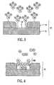
- FIG. 3is a schematic view showing deposition of a first molecule onto a substrate during sequential deposition techniques in accordance with one embodiment of the present invention
- FIG. 4is a schematic view showing deposition of second molecule onto a substrate during sequential deposition techniques in accordance with one embodiment of the present invention
- FIG. 5is a graphic representation showing the growth rate per cycle of a tantalum nitride layer versus a pre-heating temperature of a TBTDET precursor, in accordance with the present invention
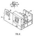
- FIG. 6is a perspective view of a semiconductor processing system in accordance with the present invention.
- FIG. 7is a detailed view of the processing chambers shown above in FIG. 6 ;
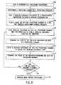
- FIG. 8is flow diagram showing a method of depositing a tantalum nitride layer, in accordance with one embodiment of the present invention.
- FIG. 9is flow diagram showing a method of depositing a tantalum nitride layer, in accordance with one embodiment of the present invention.
- FIG. 10is flow diagram showing a method of depositing a tantalum nitride layer, in accordance with one embodiment of the present invention.
- Substrate 10includes a wafer 12 that may have one or more layers, shown as layer 14 , disposed thereon.
- Wafer 12may be formed from any material suitable for semiconductor processing, such as silicon, and layer 14 may be formed from any suitable material, including dielectric or conductive materials.
- layer 14includes a void 16 , exposing a region 18 of wafer 12 .
- Embodiments of the processes described hereindeposit tantalum-containing materials or tantalum nitride on many substrates and surfaces.
- Substrates on which embodiments of the invention may be usefulinclude, but are not limited to semiconductor wafers, such as crystalline silicon (e.g., Si ⁇ 100> or Si ⁇ 111>), silicon oxide, silicon germanium, doped or undoped polysilicon, doped or undoped silicon wafers silicon nitride and patterned or non-patterned wafers.
- Surfacesinclude bare silicon wafers, films, layers and materials with dielectric, conductive and barrier properties and include aluminum oxide and polysilicon. Pretreatment of surfaces includes polishing, etching, reduction, oxidation, hydroxylation, annealing or baking the substrate.
- barrier layer 20containing a refractory metal compound, such as tantalum.
- barrier layer 20is formed from tantalum nitride, TaN, by sequentially exposing substrate 10 to processing gases to form layers of differing compounds on substrate 10 . Although not required, in this present case monolayers of differing compounds may be formed. Tantalum nitride barrier layer 20 conforms to the profile of void 16 so as to cover region 18 and layer 14 .
- a contact 22is fabricated in accordance with the present invention by formation of a copper layer 24 adjacent to barrier layer 20 , filling void 16 . Copper layer 24 may be formed using standard techniques (e.g., ALD, PVD, CVD and/or electroplating) and include seed formation and/or fill.
- Tantalum nitride barrier layer 20serves as a seed layer to promote the formation of copper layer 24 using, for example, electroplating techniques. Important characteristics that barrier layer 20 should demonstrate include good step coverage and thickness uniformity. To that end, tantalum nitride barrier layer 20 is deposited employing sequential techniques, such as atomic layer deposition.
- one example of forming barrier layer 20 employing sequential deposition techniquesincludes exposing substrate 10 to a tantalum-containing gas formed from vaporization of a liquid precursor ( t BuN)Ta(NEt 2 ) 3 (TBTDET) to form a tantalum-containing gas that includes TBTDET. It is believed that the initial surface of substrate 10 , e.g., the surface of layer 14 and region 18 , presents active ligands to the tantalum-containing gas. To that end, substrate 10 is heated within a range from about 250° C. to about 450° C. and placed in a controlled environment that is pressurized within a range from about 1 Torr to about 100 Torr, inclusive.
- a liquid precursort BuN)Ta(NEt 2 ) 3
- Substrate 10is exposed to a process gas that includes the tantalum-containing gas and a carrier gas.
- the carrier gasmay be Ar, He, N 2 , H 2 or combinations thereof and may be used as a purge gas.
- This results in a tantalum-containing layer being deposited on substrate 10 . It is believed that the tantalum-containing layer has a surface of ligands comprising amido (—NEt 2 ) and imido (N t Bu), shown generally as “a”.
- the tantalum-containing layeris exposed to another process gas that includes a nitrogen-containing gas and a carrier gas to form the tantalum-containing layer forming a barrier layer 20 of tantalum nitride.
- the nitrogen-containing gasis NH 3 gas and either Ar or N 2 is the carrier gas. It is believed that the amido and imido ligands in the exposed surface of the tantalum-containing layer react with the NH 3 process gas to form byproducts that include radicals (e.g., NH 2 , NEt 2 , N t Bu, HN t Bu or t Bu), butene, amines (e.g., HNEt 2 or H 2 N t Bu), (Et 2 N) 2 and H 2 among others. In this manner, a surface comprising a layer of tantalum nitride molecules is formed upon substrate 10 .
- radicalse.g., NH 2 , NEt 2 , N t Bu, HN t Bu or t Bu
- the tantalum nitride layermay be a monolayer of tantalum nitride molecules.
- the processproceeds cycle after cycle, until tantalum nitride barrier layer 20 has a desired thickness achieved, with each cycle having a duration from about 0.01 seconds to about 60 seconds, preferably from about 0.1 seconds to about 10 seconds, depending upon the processing system employed.
- the tantalum nitride barrier layer 20generally has a thickness in the range from about 10 ⁇ to about 1,000 ⁇ .
- Precursorsmay be a plasma, gas, liquid or solid at ambient temperature and pressure. However, within the ALD chamber, precursors are volatilized.
- Organometallic compounds or complexes that may be heated prior to deliveryinclude any chemical containing a metal and at least one organic group, such as alkyls, alkoxyls, alkylamidos and anilides. Precursors comprise of organometallic and halide compounds.
- Exemplary tantalum precursors that may be heated to form tantalum-containing gasesinclude tantalum compounds containing ligands such as alkylamidos, alkylimidos, cyclopentadienyls, halides, alkyls, alkoxides or combinations thereof.
- Alkylamido tantalum compounds used as tantalum precursorsinclude (RR′N) 5 Ta, where R or R′ are independently hydrogen, methyl, ethyl, propyl or butyl.
- Alkylimido tantalum compounds used as tantalum precursorsinclude (RN)(R′R′′N) 3 Ta, where R, R′ or R′′ are independently hydrogen, methyl, ethyl, propyl or butyl.
- tantalum precursorsinclude: (Et 2 N) 5 Ta, (Me 2 N) 5 Ta, (EtMeN) 5 Ta, (Me 5 C 5 )TaCl 4 , (acac)(EtO) 4 Ta, Br 5 Ta, Cl 5 Ta, I 5 Ta, F 5 Ta, (NO 3 ) 5 Ta, ( t BuO) 5 Ta, ( i PrO) 5 Ta, (EtO) 5 Ta and (MeO) 5 Ta.
- Exemplary nitrogen precursors utilized in nitrogen-containing gasesinclude: NH 3 , N 2 , hydrazines (e.g., N 2 H 4 or MeN 2 H 3 ), amines (e.g., Me 3 N, Me 2 NH or MeNH 2 ), anilines (e.g., C 6 H 5 NH 2 ), organic azides (e.g., MeN 3 or Me 3 SiN 3 ), inorganic azides (e.g., NaN 3 or Cp 2 CoN 3 ) and radical nitrogen compounds (e.g., N 3 , N 2 , N, NH or NH 2 ). Radical nitrogen compounds can be produced by heat, hot-wires and/or plasma.
- hydrazinese.g., N 2 H 4 or MeN 2 H 3
- aminese.g., Me 3 N, Me 2 NH or MeNH 2
- anilinese.g., C 6 H 5 NH 2
- organic azidese.g., MeN 3 or Me
- the time required to form tantalum nitride barrier layer 20may be reduced by heating the TBTDET precursor before formation of the tantalum-containing layer on substrate 10 .
- curve 30it was found that by heating the TBTDET precursor in the range from about 65° C. to about 150° C., shown as segment 32 , the growth rate of the layers of tantalum nitride per ALD cycle may be maximized.
- point 34shows the growth rate at about 65° C. being a little less than about 0.9 ⁇ per cycle.
- Point 36shows the growth rate at about 90° C. being a little less than about 1.2 ⁇ per cycle
- point 38shows the growth rate at about 150° C.
- a segment 40 of curve 30shows that for temperatures below about 65° C., the growth rate of tantalum nitride is substantially reduced.
- a segment 42 of curve 30shows that for temperatures above about 150° C., the growth rate of tantalum nitride is substantially reduced.
- the slope of a segment 32 of curve 30shows that the growth rate of tantalum nitride barrier layer 20 is greater for temperatures within a range from about 65° C. to about 150° C. compared to other temperatures for the TBTDET precursor.
- an exemplary wafer processing system employed to deposit a tantalum nitride layer in accordance with the present inventionincludes one or more processing chambers 44 , 45 and 46 .
- Processing chambers 44 , 45 and 46are disposed in a common work area 48 surrounded by a wall 50 .
- Processing chambers 44 , 45 and 46are in data communication with a controller 54 that is connected to one or more monitors, shown as 56 and 58 .
- Monitors 56 and 58typically display common information concerning the process associated with the processing chambers 44 , 45 and 46 .
- Monitor 58is mounted to the wall 50 , with monitor 56 being disposed in the work area 48 .
- Operational control of processing chambers 44 , 45 and 46may be achieved with use of a light pen, associated with one of monitors 56 and 58 , to communicate with controller 54 .
- a light pen 60 ais associated with monitor 56 and facilitates communication with the controller 54 through monitor 56 .
- a light pen 60 bfacilitates communication with controller 54 through monitor 58 .
- each of processing chambers 44 , 45 and 46includes a housing 62 having a base wall 64 , a cover 66 , disposed opposite to base wall 64 , and a sidewall 67 , extending there between.
- Housing 62defines a chamber 68 .
- a pedestal 69is disposed within processing chamber 68 to support substrate 10 .
- Pedestal 69may be mounted to move between cover 66 and base wall 64 , using a displacement mechanism (not shown), but is typically fixed proximate to base wall 64 .
- Supplies of processing fluids 70 a , 70 b , 70 c and 71are in fluid communication with processing chamber 68 via a manifold 72 .
- supply 70 amay contain NH 3
- supply 70 bmay contain N 2
- supply 70 cmay contain Ar.
- Process fluid supply 71includes an ampoule 71 a in fluid communication with a vaporizer 71 b .
- Ampoule 71 aincludes a supply of TBTDET precursor 71 c and is in fluid communication with supply 70 c .
- Ampoule 71 ais in fluid communication with vaporizer 71 b via precursor channel 71 d to deliver, to processing chamber 68 , precursor 71 c , with the aid of carrier gas in supply 70 c .
- Ampoule 71 a , liquid 71 c and channel 71 dmay be heated by conventional heating methods, e.g., heating tape in the range from about 65° C. to about 150° C. Regulation of the flow of gases from supplies 70 a , 70 b , 70 c and 71 is effectuated via flow valves 73 that are regulated by computer control, discussed more fully below.
- Flow valves 73may be any suitable valve. Actuation rates of flow valves 73 may be in the range of a microsecond to several milliseconds to seconds.
- Substrate 10is heated to processing temperature by a heater embedded within pedestal 69 .
- pedestal 69may be resistively heated by applying an electric current from an AC power supply 75 to a heater element 76 .
- Substrate 10is, in turn, heated by pedestal 69 , and can be maintained within a desired process temperature range, with the actual temperature varying dependent upon the gases employed and the topography of the surface upon which deposition is to occur.
- a temperature sensor 78such as a thermocouple, is also embedded in pedestal 69 to monitor the temperature of pedestal 69 in a conventional manner.
- the measured temperaturemay be used in a feedback loop to control the electrical current applied to heater element 76 by power supply 75 , such that the wafer temperature can be maintained or controlled at a desired temperature that is suitable for the particular process application.
- Substrate 10may be heated using radiant heat, e.g., heat lamps or plasma (not shown).
- a vacuum pump 80is used to evacuate processing chamber 68 and to help maintain the proper gas flows and pressure inside processing chamber 68 .
- a method in accordance with one embodiment of the present inventionincludes heating substrate 10 to a processing temperature within a range from about 250° C. to about 450° C. at step 100 .
- processing chamber 68is pressurized within a range from about 1 Torr to about 100 Torr. This is achieved by activating vacuum pump 80 to evacuate processing chamber 68 .
- the TBTDET precursoris heated in ampoule 71 a within a range from about 65° C. to about 150° C. This forms a tantalum-containing gas that includes TBTDET.
- a purge gassuch as argon, Ar
- argonAr
- the actual time during which Ar is flowed into processing chamber 68is dependent upon the system employed.
- Aris flowed into processing chamber 68 in a range of from about 5 to about 10 seconds to purge processing chamber 68 .
- the tantalum-containing gasis flowed into processing chamber 68 along with Ar gas to create a tantalum-containing layer on substrate 10 that includes TBTDET.
- Ar gas from supply 70 cis flowed into ampoule 71 a at a rate in the range from about 50 sccm to about 2,000 sccm, preferably about 500 sccm.
- the flow of tantalum-containing gasis terminated, at step 110 .
- the flow of tantalum-containing gasis terminated after about 5 seconds to about 25 seconds after the flow commenced.
- the flow of Ar gasmay terminate with the flow of tantalum-containing gas.
- the flow of Ar gasmay continue for a sufficient amount of time, depending upon the processing system employed, to ensure removal from processing chamber 68 of tantalum-containing gas and reaction byproducts, at step 110 .
- the time that the flow of Ar gas continuesis in the range from about 5 seconds to about 10 seconds.
- a nitrogen-containing gassuch as NH 3 gas
- NH 3 gasis pulsed into processing chamber 68 , along with the purge gas for a sufficient amount of time to create a reaction between nitrogen, in the NH 3 gas, and the tantalum-containing layer to form a layer of tantalum nitride.
- the resulting layer of tantalum nitridemay be a monolayer of tantalum nitride molecules.
- the duration of the pulse of NH 3 gasis dependent upon the processing system employed, but in the present example the flow of NH 3 gas was in the range from about 5 seconds to about 35 seconds.
- the pulse of the nitrogen-containing gas into processing chamber 68is subsequently terminated, at step 114 .
- the flow of the purge gasmay be terminated along with the flow of the nitrogen-containing gas. Alternatively, the flow of the purge gas may continue at step 114 . In this manner, NH 3 gas and byproducts of the reaction of nitrogen with the tantalum-containing layer are removed from processing chamber 68 .
- each cycleresults in the formation of a tantalum nitride layer having a thickness within a range from about 0.9 ⁇ to about 1.2 ⁇ .
- a desired thicknessemploying any known means in the art. Were it determined that the tantalum nitride layer had not reached a desired thickness, then the process would proceed to step 108 . Were it determined that tantalum nitride layer had reached a desired thickness, then the process would proceed with further processing at step 118 .
- An example of further processingcould include formation of a copper layer 24 , shown in FIG. 2 , employing standard formation techniques, such as electroplating. Further processing includes a seed layer or a nucleation layer 23 deposited on the barrier layer 20 via ALD, CVD or PVD techniques.
- controller 54includes a central processing unit (CPU) 90 , a volatile memory, such as a random access memory (RAM) 92 and permanent storage media, such as a floppy disk drive for use with a floppy diskette, or hard disk drive 94 .
- the computer program codecan be written in any conventional computer readable programming language; for example, 68000 assembly language, C, C++, Pascal, Fortran, and the like.
- Suitable program codeis entered into a single file, or multiple files, using a conventional text editor and stored or embodied in a computer-readable medium, such as the hard disk drive 94 . If the entered code text is in a high level language, the code is compiled and the resultant compiler code is then linked with an object code of precompiled Windows® library routines. To execute the linked and compiled object code the system user invokes the object code, causing CPU 90 to load the code in RAM 92 . CPU 90 then reads and executes the code to perform the tasks identified in the program.
- a method in accordance with an alternate embodimentovercomes difficulty in having vacuum pump 80 establish the processing pressure during the differing processing steps of the sequential deposition process. Specifically, it was found that relying on vacuum pump 80 to establish the processing pressure might increase the time required to form a tantalum nitride layer. This is due, in part, to the time required for vacuum pump 80 to stabilize (settle) in order to evacuate at a constant rate and thus pump down the processing chamber 68 to establish the processing pressure. To avoid the pump stabilization problem, vacuum pump 80 may be set to evacuate processing chamber 68 at a constant rate throughout the sequential deposition process. Thereafter, the processing pressure would be established by the flow rates of the process gases into process chamber 68 .
- substrate 10is heated to a processing temperature within a range from about 250° C. to about 450° C.
- the pumpis activated to evacuate processing chamber 68 at a constant rate.
- the TBTDET precursoris heated in ampoule 71 a within a range from 65° C. to about 150° C. This forms a tantalum-containing gas that includes TBTDET.
- a purge gassuch as argon, is flowed into processing chamber 68 for a sufficient time to purge processing chamber 68 and establish a processing pressure.
- the processing pressureis within a range from about 1 Torr to about 100 Torr.
- the tantalum-containing gasis flowed into processing chamber 68 along with Ar gas to create a tantalum-containing layer on substrate 10 .
- the flow rates of the tantalum-containing gas and the Ar gasis established so as to prevent varying the processing pressure established at step 206 .
- Ar gas from supply 70 cis flowed into ampoule 71 a at a rate of approximately 500 sccm.
- the flow of tantalum-containing gasis terminated, with the flow of Ar increased to maintain the processing pressure, at step 210 . This continues for a sufficient time to remove tantalum-containing gas and reaction byproducts from processing chamber 68 , typically about 5 seconds to about 10 seconds.
- a nitrogen-containing gassuch as NH 3 gas
- NH 3 gasis introduced into processing chamber 68 , along with the purge gas for a sufficient amount of time to react nitrogen, contained in the nitrogen-containing gas, with the tantalum-containing layer to form a tantalum nitride layer.
- the tantalum nitride layermay or may not be a monolayer of tantalum nitride molecules.
- the time required to achieve the nitrogen reactiondepends upon the processing system employed. In the present example, the time is in the range from about 5 seconds to about 35 seconds.
- the flow rate of the NH 3 gas and the purge gasare established so that the processing pressure established at step 206 is maintained.
- the flow of the NH 3 process gas into processing chamber 68is subsequently terminated, while the flow of purge gas is increased at step 214 to maintain a constant processing pressure. In this manner, the nitrogen-containing gas and byproducts of the nitrogen reaction with the tantalum-containing layer are removed from processing chamber 68 . This completes one cycle of the sequential deposition technique in accordance with the present invention.
- the tantalum nitride barrier layeris grown to a thickness in the range from about 10 ⁇ to about 1,000 ⁇ .
- An example of further processingcould include formation of a copper layer 24 , shown in FIG. 2 , employing standard formation techniques, such as electroplating.
- removal of byproducts and precursors from processing chamber 68may be achieved by evacuating processing chamber 68 of all gases present after formation of each tantalum-containing layer that is yet to under go a reaction with nitrogen.
- substrate 10is heated to a processing temperature within a range from about 250° C. to about 450° C. at step 300 , and the TBTDET precursor is heated in ampoule 71 a within a range from about 65° C. to about 150° C. at step 302 to form a tantalum-containing gas that includes TBTDET.
- vacuum pump 80establishes a processing pressure within a range from about 1 Torr to about 100 Torr.
- a purge gas, such as argonis flowed into processing chamber 68 for a sufficient amount of time to purge processing chamber 68 . The time required to purge processing chamber 68 is dependent upon the processing system employed.
- the time required to purge processing chamber 68is within a range from about 5 seconds to about 10 seconds.
- the tantalum-containing gasis flowed into processing chamber 68 along with Ar gas to create a tantalum-containing layer on substrate 10 .
- Ar gas from supply 70 cis flowed into ampoule 71 a at a rate of approximately 500 sccm.
- the flow of tantalum-containing gasis terminated, while the flow of Ar continues.
- the amount of time during which the tantalum-containing gas flowsis dependent upon the processing system employed.
- the tantalum-containing gasis flowed into processing chamber 68 for approximately 5 seconds to about 25 seconds during step 310 .
- the flow of Ar gas into processing chamber 68continues for a sufficient time to remove the tantalum-containing gas and reaction byproducts from processing chamber 68 .
- the duration for which Ar gas is flowed into processing chamber 68is dependent upon the processing system employed, but in the present example, is in the range from about 5 seconds to about 25 seconds.
- step 312the flow of Ar gas is terminated and the processing chamber is evacuated of all gases present.
- processing chamber 68is brought to the processing pressure and the Ar gas is introduced therein.
- the nitrogen-containing gasis introduced into processing chamber 68 , along with the purge gas for a sufficient amount of time to react nitrogen in the nitrogen-containing gas with the tantalum-containing layer to form a layer of tantalum nitride. The time required to achieve the nitrogen reaction is dependent upon the processing system employed.
- the nitrogen-containing gasis flowed into processing chamber 68 in the range from 5 seconds to about 35 seconds during step 316 .
- the flow of the tantalum-containing process gas into processing chamber 68is subsequently terminated, while the flow of purge gas continues at step 318 .
- the tantalum-containing process gas and byproducts of the nitrogen reactionare removed from processing chamber 68 .
- the flow of Ar gasis terminated and the processing chamber is evacuated of all gases present therein at step 312 . This completes one cycle of the sequential deposition technique in accordance with the present invention.
- step 322it is determined whether the aforementioned tantalum nitride layer has reached a desired thickness employing any known means in the art. Were it determined that tantalum nitride layer had not reached a desired thickness, and then the process would proceed to step 304 . Were it determined that tantalum nitride layer had reached a desired thickness, and then the process would proceed with further processing at step 324 .
- An example of further processingcould include formation of a copper layer 24 , shown in FIG. 2 , employing standard formation techniques, such as electroplating.
- tantalum nitrideis formed with stoichiometry that includes TaN x , were x is in the range from about 0.4 to about 2. Tantalum nitride is often derived with the empirical formulas TaN, Ta 3 N 5 Ta 2 N or Ta 6 N 2.57 . Tantalum nitride is deposited as amorphous or crystalline material. In some metal nitrides, slight variations of the stoichiometry can have a large impact on the electrical properties, e.g., Hf 3 N 4 is an insulator while HfN is a conductor. Therefore, ALD provides stoichiometric control during the deposition of product compounds. The stoichiometry may be altered by various procedures following the deposition process, such as when Ta 3 N 5 is thermally annealed to form TaN. Altering the precursor ratios during deposition also controls stoichiometry.
- the product compoundsmay be used as seed layers, diffusion barrier layers, adhesion layers, insulator layers, conducting layers or functionalized surface groups for patterned surfaces (e.g., selective deposition).
- reaction conditionse.g., temperature, pressure, film thickness and the like
- sequential deposition processmay have different initial sequence.
- the initial sequencemay include exposing the substrate to the reducing gas before the metal-containing gas is introduced into the processing chamber.
- the tantalum nitride layermay be employed for other features of circuits in addition to functioning as a diffusion barrier for contacts. Therefore, the scope of the invention should not be based upon the foregoing description. Rather, the scope of the invention should be determined based upon the claims recited herein, including the full scope of equivalents thereof.
Landscapes
- Chemical & Material Sciences (AREA)
- Engineering & Computer Science (AREA)
- General Chemical & Material Sciences (AREA)
- Chemical Kinetics & Catalysis (AREA)
- Materials Engineering (AREA)
- Mechanical Engineering (AREA)
- Metallurgy (AREA)
- Organic Chemistry (AREA)
- Physics & Mathematics (AREA)
- Condensed Matter Physics & Semiconductors (AREA)
- General Physics & Mathematics (AREA)
- Manufacturing & Machinery (AREA)
- Computer Hardware Design (AREA)
- Microelectronics & Electronic Packaging (AREA)
- Power Engineering (AREA)
- Inorganic Chemistry (AREA)
- Chemical Vapour Deposition (AREA)
- Electrodes Of Semiconductors (AREA)
- Internal Circuitry In Semiconductor Integrated Circuit Devices (AREA)
Abstract
Description
Claims (17)
Priority Applications (2)
| Application Number | Priority Date | Filing Date | Title |
|---|---|---|---|
| US12/417,439US7867896B2 (en) | 2002-03-04 | 2009-04-02 | Sequential deposition of tantalum nitride using a tantalum-containing precursor and a nitrogen-containing precursor |
| US12/914,937US20110070730A1 (en) | 2002-03-04 | 2010-10-28 | Sequential deposition of tantalum nitride using a tantalum-containing precursor and a nitrogen-containing precursor |
Applications Claiming Priority (4)
| Application Number | Priority Date | Filing Date | Title |
|---|---|---|---|
| US36218902P | 2002-03-04 | 2002-03-04 | |
| US10/379,438US6972267B2 (en) | 2002-03-04 | 2003-03-04 | Sequential deposition of tantalum nitride using a tantalum-containing precursor and a nitrogen-containing precursor |
| US11/231,386US7514358B2 (en) | 2002-03-04 | 2005-09-21 | Sequential deposition of tantalum nitride using a tantalum-containing precursor and a nitrogen-containing precursor |
| US12/417,439US7867896B2 (en) | 2002-03-04 | 2009-04-02 | Sequential deposition of tantalum nitride using a tantalum-containing precursor and a nitrogen-containing precursor |
Related Parent Applications (1)
| Application Number | Title | Priority Date | Filing Date |
|---|---|---|---|
| US11/231,386ContinuationUS7514358B2 (en) | 2002-03-04 | 2005-09-21 | Sequential deposition of tantalum nitride using a tantalum-containing precursor and a nitrogen-containing precursor |
Related Child Applications (1)
| Application Number | Title | Priority Date | Filing Date |
|---|---|---|---|
| US12/914,937ContinuationUS20110070730A1 (en) | 2002-03-04 | 2010-10-28 | Sequential deposition of tantalum nitride using a tantalum-containing precursor and a nitrogen-containing precursor |
Publications (2)
| Publication Number | Publication Date |
|---|---|
| US20090197406A1 US20090197406A1 (en) | 2009-08-06 |
| US7867896B2true US7867896B2 (en) | 2011-01-11 |
Family
ID=29586722
Family Applications (4)
| Application Number | Title | Priority Date | Filing Date |
|---|---|---|---|
| US10/379,438Expired - LifetimeUS6972267B2 (en) | 2002-03-04 | 2003-03-04 | Sequential deposition of tantalum nitride using a tantalum-containing precursor and a nitrogen-containing precursor |
| US11/231,386Expired - LifetimeUS7514358B2 (en) | 2002-03-04 | 2005-09-21 | Sequential deposition of tantalum nitride using a tantalum-containing precursor and a nitrogen-containing precursor |
| US12/417,439Expired - LifetimeUS7867896B2 (en) | 2002-03-04 | 2009-04-02 | Sequential deposition of tantalum nitride using a tantalum-containing precursor and a nitrogen-containing precursor |
| US12/914,937AbandonedUS20110070730A1 (en) | 2002-03-04 | 2010-10-28 | Sequential deposition of tantalum nitride using a tantalum-containing precursor and a nitrogen-containing precursor |
Family Applications Before (2)
| Application Number | Title | Priority Date | Filing Date |
|---|---|---|---|
| US10/379,438Expired - LifetimeUS6972267B2 (en) | 2002-03-04 | 2003-03-04 | Sequential deposition of tantalum nitride using a tantalum-containing precursor and a nitrogen-containing precursor |
| US11/231,386Expired - LifetimeUS7514358B2 (en) | 2002-03-04 | 2005-09-21 | Sequential deposition of tantalum nitride using a tantalum-containing precursor and a nitrogen-containing precursor |
Family Applications After (1)
| Application Number | Title | Priority Date | Filing Date |
|---|---|---|---|
| US12/914,937AbandonedUS20110070730A1 (en) | 2002-03-04 | 2010-10-28 | Sequential deposition of tantalum nitride using a tantalum-containing precursor and a nitrogen-containing precursor |
Country Status (1)
| Country | Link |
|---|---|
| US (4) | US6972267B2 (en) |
Cited By (2)
| Publication number | Priority date | Publication date | Assignee | Title |
|---|---|---|---|---|
| US20110070730A1 (en)* | 2002-03-04 | 2011-03-24 | Wei Cao | Sequential deposition of tantalum nitride using a tantalum-containing precursor and a nitrogen-containing precursor |
| US10636705B1 (en) | 2018-11-29 | 2020-04-28 | Applied Materials, Inc. | High pressure annealing of metal gate structures |
Families Citing this family (121)
| Publication number | Priority date | Publication date | Assignee | Title |
|---|---|---|---|---|
| US6974766B1 (en) | 1998-10-01 | 2005-12-13 | Applied Materials, Inc. | In situ deposition of a low κ dielectric layer, barrier layer, etch stop, and anti-reflective coating for damascene application |
| US6620723B1 (en) | 2000-06-27 | 2003-09-16 | Applied Materials, Inc. | Formation of boride barrier layers using chemisorption techniques |
| US7405158B2 (en) | 2000-06-28 | 2008-07-29 | Applied Materials, Inc. | Methods for depositing tungsten layers employing atomic layer deposition techniques |
| US7101795B1 (en) | 2000-06-28 | 2006-09-05 | Applied Materials, Inc. | Method and apparatus for depositing refractory metal layers employing sequential deposition techniques to form a nucleation layer |
| US6551929B1 (en) | 2000-06-28 | 2003-04-22 | Applied Materials, Inc. | Bifurcated deposition process for depositing refractory metal layers employing atomic layer deposition and chemical vapor deposition techniques |
| US6951804B2 (en)* | 2001-02-02 | 2005-10-04 | Applied Materials, Inc. | Formation of a tantalum-nitride layer |
| US20090004850A1 (en) | 2001-07-25 | 2009-01-01 | Seshadri Ganguli | Process for forming cobalt and cobalt silicide materials in tungsten contact applications |
| JP2005504885A (en) | 2001-07-25 | 2005-02-17 | アプライド マテリアルズ インコーポレイテッド | Barrier formation using a novel sputter deposition method |
| US9051641B2 (en) | 2001-07-25 | 2015-06-09 | Applied Materials, Inc. | Cobalt deposition on barrier surfaces |
| US20030029715A1 (en) | 2001-07-25 | 2003-02-13 | Applied Materials, Inc. | An Apparatus For Annealing Substrates In Physical Vapor Deposition Systems |
| US8110489B2 (en) | 2001-07-25 | 2012-02-07 | Applied Materials, Inc. | Process for forming cobalt-containing materials |
| US8026161B2 (en) | 2001-08-30 | 2011-09-27 | Micron Technology, Inc. | Highly reliable amorphous high-K gate oxide ZrO2 |
| US6936906B2 (en) | 2001-09-26 | 2005-08-30 | Applied Materials, Inc. | Integration of barrier layer and seed layer |
| US7049226B2 (en) | 2001-09-26 | 2006-05-23 | Applied Materials, Inc. | Integration of ALD tantalum nitride for copper metallization |
| US7780785B2 (en) | 2001-10-26 | 2010-08-24 | Applied Materials, Inc. | Gas delivery apparatus for atomic layer deposition |
| US6916398B2 (en) | 2001-10-26 | 2005-07-12 | Applied Materials, Inc. | Gas delivery apparatus and method for atomic layer deposition |
| US7081271B2 (en) | 2001-12-07 | 2006-07-25 | Applied Materials, Inc. | Cyclical deposition of refractory metal silicon nitride |
| US6767795B2 (en) | 2002-01-17 | 2004-07-27 | Micron Technology, Inc. | Highly reliable amorphous high-k gate dielectric ZrOXNY |
| US6911391B2 (en) | 2002-01-26 | 2005-06-28 | Applied Materials, Inc. | Integration of titanium and titanium nitride layers |
| US6833161B2 (en) | 2002-02-26 | 2004-12-21 | Applied Materials, Inc. | Cyclical deposition of tungsten nitride for metal oxide gate electrode |
| KR100476556B1 (en)* | 2002-04-11 | 2005-03-18 | 삼성전기주식회사 | Piezoelectric transformer, housing for piezoelectric transformer and manufacture thereof |
| US7279432B2 (en) | 2002-04-16 | 2007-10-09 | Applied Materials, Inc. | System and method for forming an integrated barrier layer |
| US7589029B2 (en) | 2002-05-02 | 2009-09-15 | Micron Technology, Inc. | Atomic layer deposition and conversion |
| US7160577B2 (en) | 2002-05-02 | 2007-01-09 | Micron Technology, Inc. | Methods for atomic-layer deposition of aluminum oxides in integrated circuits |
| US7404985B2 (en) | 2002-06-04 | 2008-07-29 | Applied Materials, Inc. | Noble metal layer formation for copper film deposition |
| US7221586B2 (en) | 2002-07-08 | 2007-05-22 | Micron Technology, Inc. | Memory utilizing oxide nanolaminates |
| US6838125B2 (en) | 2002-07-10 | 2005-01-04 | Applied Materials, Inc. | Method of film deposition using activated precursor gases |
| US7186385B2 (en) | 2002-07-17 | 2007-03-06 | Applied Materials, Inc. | Apparatus for providing gas to a processing chamber |
| US7084078B2 (en) | 2002-08-29 | 2006-08-01 | Micron Technology, Inc. | Atomic layer deposited lanthanide doped TiOx dielectric films |
| EP1420080A3 (en) | 2002-11-14 | 2005-11-09 | Applied Materials, Inc. | Apparatus and method for hybrid chemical deposition processes |
| US7244683B2 (en) | 2003-01-07 | 2007-07-17 | Applied Materials, Inc. | Integration of ALD/CVD barriers with porous low k materials |
| US7262133B2 (en)* | 2003-01-07 | 2007-08-28 | Applied Materials, Inc. | Enhancement of copper line reliability using thin ALD tan film to cap the copper line |
| US7192892B2 (en) | 2003-03-04 | 2007-03-20 | Micron Technology, Inc. | Atomic layer deposited dielectric layers |
| US7135369B2 (en) | 2003-03-31 | 2006-11-14 | Micron Technology, Inc. | Atomic layer deposited ZrAlxOy dielectric layers including Zr4AlO9 |
| US7183186B2 (en) | 2003-04-22 | 2007-02-27 | Micro Technology, Inc. | Atomic layer deposited ZrTiO4 films |
| US7211508B2 (en) | 2003-06-18 | 2007-05-01 | Applied Materials, Inc. | Atomic layer deposition of tantalum based barrier materials |
| US7235482B2 (en)* | 2003-09-08 | 2007-06-26 | Taiwan Semiconductor Manufacturing Company, Ltd. | Method of manufacturing a contact interconnection layer containing a metal and nitrogen by atomic layer deposition for deep sub-micron semiconductor technology |
| US20050252449A1 (en) | 2004-05-12 | 2005-11-17 | Nguyen Son T | Control of gas flow and delivery to suppress the formation of particles in an MOCVD/ALD system |
| US8323754B2 (en) | 2004-05-21 | 2012-12-04 | Applied Materials, Inc. | Stabilization of high-k dielectric materials |
| US7211507B2 (en)* | 2004-06-02 | 2007-05-01 | International Business Machines Corporation | PE-ALD of TaN diffusion barrier region on low-k materials |
| US7605469B2 (en)* | 2004-06-30 | 2009-10-20 | Intel Corporation | Atomic layer deposited tantalum containing adhesion layer |
| US7241686B2 (en) | 2004-07-20 | 2007-07-10 | Applied Materials, Inc. | Atomic layer deposition of tantalum-containing materials using the tantalum precursor TAIMATA |
| US7588988B2 (en) | 2004-08-31 | 2009-09-15 | Micron Technology, Inc. | Method of forming apparatus having oxide films formed using atomic layer deposition |
| KR100552820B1 (en)* | 2004-09-17 | 2006-02-21 | 동부아남반도체 주식회사 | Manufacturing Method of Semiconductor Device |
| US7429402B2 (en)* | 2004-12-10 | 2008-09-30 | Applied Materials, Inc. | Ruthenium as an underlayer for tungsten film deposition |
| US7078326B1 (en)* | 2005-01-19 | 2006-07-18 | Marsh Eugene P | Nucleation method for atomic layer deposition of cobalt on bare silicon during the formation of a semiconductor device |
| US7687409B2 (en) | 2005-03-29 | 2010-03-30 | Micron Technology, Inc. | Atomic layer deposited titanium silicon oxide films |
| US7662729B2 (en) | 2005-04-28 | 2010-02-16 | Micron Technology, Inc. | Atomic layer deposition of a ruthenium layer to a lanthanide oxide dielectric layer |
| US20070001231A1 (en)* | 2005-06-29 | 2007-01-04 | Amberwave Systems Corporation | Material systems for dielectrics and metal electrodes |
| US7432139B2 (en) | 2005-06-29 | 2008-10-07 | Amberwave Systems Corp. | Methods for forming dielectrics and metal electrodes |
| US20070020890A1 (en)* | 2005-07-19 | 2007-01-25 | Applied Materials, Inc. | Method and apparatus for semiconductor processing |
| US7927948B2 (en) | 2005-07-20 | 2011-04-19 | Micron Technology, Inc. | Devices with nanocrystals and methods of formation |
| US8110469B2 (en) | 2005-08-30 | 2012-02-07 | Micron Technology, Inc. | Graded dielectric layers |
| US20070054487A1 (en)* | 2005-09-06 | 2007-03-08 | Applied Materials, Inc. | Atomic layer deposition processes for ruthenium materials |
| US20070077750A1 (en)* | 2005-09-06 | 2007-04-05 | Paul Ma | Atomic layer deposition processes for ruthenium materials |
| US20070065576A1 (en)* | 2005-09-09 | 2007-03-22 | Vikram Singh | Technique for atomic layer deposition |
| US8993055B2 (en) | 2005-10-27 | 2015-03-31 | Asm International N.V. | Enhanced thin film deposition |
| TWI332532B (en)* | 2005-11-04 | 2010-11-01 | Applied Materials Inc | Apparatus and process for plasma-enhanced atomic layer deposition |
| US20070252299A1 (en)* | 2006-04-27 | 2007-11-01 | Applied Materials, Inc. | Synchronization of precursor pulsing and wafer rotation |
| US20070259111A1 (en)* | 2006-05-05 | 2007-11-08 | Singh Kaushal K | Method and apparatus for photo-excitation of chemicals for atomic layer deposition of dielectric film |
| US7798096B2 (en) | 2006-05-05 | 2010-09-21 | Applied Materials, Inc. | Plasma, UV and ion/neutral assisted ALD or CVD in a batch tool |
| TWI395335B (en)* | 2006-06-30 | 2013-05-01 | Applied Materials Inc | Formation of nanocrystals |
| WO2008013659A2 (en)* | 2006-07-21 | 2008-01-31 | The Boc Group, Inc. | Single precursors for atomic layer deposition |
| US8268409B2 (en)* | 2006-10-25 | 2012-09-18 | Asm America, Inc. | Plasma-enhanced deposition of metal carbide films |
| US7611751B2 (en) | 2006-11-01 | 2009-11-03 | Asm America, Inc. | Vapor deposition of metal carbide films |
| KR101482805B1 (en)* | 2006-12-28 | 2015-01-14 | 엑사테크 엘.엘.씨. | Apparatus and method for plasma arc coating |
| US7595270B2 (en)* | 2007-01-26 | 2009-09-29 | Asm America, Inc. | Passivated stoichiometric metal nitride films |
| US7598170B2 (en)* | 2007-01-26 | 2009-10-06 | Asm America, Inc. | Plasma-enhanced ALD of tantalum nitride films |
| US7713874B2 (en) | 2007-05-02 | 2010-05-11 | Asm America, Inc. | Periodic plasma annealing in an ALD-type process |
| US7678298B2 (en) | 2007-09-25 | 2010-03-16 | Applied Materials, Inc. | Tantalum carbide nitride materials by vapor deposition processes |
| US7585762B2 (en) | 2007-09-25 | 2009-09-08 | Applied Materials, Inc. | Vapor deposition processes for tantalum carbide nitride materials |
| US7824743B2 (en) | 2007-09-28 | 2010-11-02 | Applied Materials, Inc. | Deposition processes for titanium nitride barrier and aluminum |
| US7737028B2 (en)* | 2007-09-28 | 2010-06-15 | Applied Materials, Inc. | Selective ruthenium deposition on copper materials |
| KR101540077B1 (en)* | 2008-04-16 | 2015-07-28 | 에이에스엠 아메리카, 인코포레이티드 | Atomic layer deposition of metal carbide films using aluminum hydrocarbon compounds |
| US7666474B2 (en) | 2008-05-07 | 2010-02-23 | Asm America, Inc. | Plasma-enhanced pulsed deposition of metal carbide films |
| US20100037824A1 (en)* | 2008-08-13 | 2010-02-18 | Synos Technology, Inc. | Plasma Reactor Having Injector |
| US20100037820A1 (en)* | 2008-08-13 | 2010-02-18 | Synos Technology, Inc. | Vapor Deposition Reactor |
| US20100062149A1 (en) | 2008-09-08 | 2010-03-11 | Applied Materials, Inc. | Method for tuning a deposition rate during an atomic layer deposition process |
| US8491967B2 (en) | 2008-09-08 | 2013-07-23 | Applied Materials, Inc. | In-situ chamber treatment and deposition process |
| US8851012B2 (en)* | 2008-09-17 | 2014-10-07 | Veeco Ald Inc. | Vapor deposition reactor using plasma and method for forming thin film using the same |
| US8770142B2 (en)* | 2008-09-17 | 2014-07-08 | Veeco Ald Inc. | Electrode for generating plasma and plasma generator |
| US8146896B2 (en) | 2008-10-31 | 2012-04-03 | Applied Materials, Inc. | Chemical precursor ampoule for vapor deposition processes |
| US8871628B2 (en)* | 2009-01-21 | 2014-10-28 | Veeco Ald Inc. | Electrode structure, device comprising the same and method for forming electrode structure |
| US8557702B2 (en)* | 2009-02-02 | 2013-10-15 | Asm America, Inc. | Plasma-enhanced atomic layers deposition of conductive material over dielectric layers |
| US8257799B2 (en) | 2009-02-23 | 2012-09-04 | Synos Technology, Inc. | Method for forming thin film using radicals generated by plasma |
| US8758512B2 (en)* | 2009-06-08 | 2014-06-24 | Veeco Ald Inc. | Vapor deposition reactor and method for forming thin film |
| US8771791B2 (en) | 2010-10-18 | 2014-07-08 | Veeco Ald Inc. | Deposition of layer using depositing apparatus with reciprocating susceptor |
| US8877300B2 (en)* | 2011-02-16 | 2014-11-04 | Veeco Ald Inc. | Atomic layer deposition using radicals of gas mixture |
| US9163310B2 (en) | 2011-02-18 | 2015-10-20 | Veeco Ald Inc. | Enhanced deposition of layer on substrate using radicals |
| US9412602B2 (en) | 2013-03-13 | 2016-08-09 | Asm Ip Holding B.V. | Deposition of smooth metal nitride films |
| US8841182B1 (en) | 2013-03-14 | 2014-09-23 | Asm Ip Holding B.V. | Silane and borane treatments for titanium carbide films |
| US8846550B1 (en) | 2013-03-14 | 2014-09-30 | Asm Ip Holding B.V. | Silane or borane treatment of metal thin films |
| US10106887B2 (en)* | 2013-11-13 | 2018-10-23 | L'Air Liquide, Société Anonyme pour l'Etude et l'Exploitation des Procédés Georges Claude | Group 5 transition metal-containing compounds for vapor deposition of group 5 transition metal-containing films |
| US9376455B2 (en) | 2013-11-27 | 2016-06-28 | Veeco Ald Inc. | Molecular layer deposition using reduction process |
| US9394609B2 (en) | 2014-02-13 | 2016-07-19 | Asm Ip Holding B.V. | Atomic layer deposition of aluminum fluoride thin films |
| US10643925B2 (en) | 2014-04-17 | 2020-05-05 | Asm Ip Holding B.V. | Fluorine-containing conductive films |
| US10002936B2 (en) | 2014-10-23 | 2018-06-19 | Asm Ip Holding B.V. | Titanium aluminum and tantalum aluminum thin films |
| US9941425B2 (en) | 2015-10-16 | 2018-04-10 | Asm Ip Holdings B.V. | Photoactive devices and materials |
| US9786491B2 (en) | 2015-11-12 | 2017-10-10 | Asm Ip Holding B.V. | Formation of SiOCN thin films |
| US9786492B2 (en) | 2015-11-12 | 2017-10-10 | Asm Ip Holding B.V. | Formation of SiOCN thin films |
| KR102378021B1 (en) | 2016-05-06 | 2022-03-23 | 에이에스엠 아이피 홀딩 비.브이. | Formation of SiOC thin films |
| US10186420B2 (en) | 2016-11-29 | 2019-01-22 | Asm Ip Holding B.V. | Formation of silicon-containing thin films |
| US10847529B2 (en) | 2017-04-13 | 2020-11-24 | Asm Ip Holding B.V. | Substrate processing method and device manufactured by the same |
| US10504901B2 (en) | 2017-04-26 | 2019-12-10 | Asm Ip Holding B.V. | Substrate processing method and device manufactured using the same |
| CN114875388A (en) | 2017-05-05 | 2022-08-09 | Asm Ip 控股有限公司 | Plasma enhanced deposition method for controlled formation of oxygen-containing films |
| US10276411B2 (en) | 2017-08-18 | 2019-04-30 | Applied Materials, Inc. | High pressure and high temperature anneal chamber |
| TWI761636B (en) | 2017-12-04 | 2022-04-21 | 荷蘭商Asm Ip控股公司 | PLASMA ENHANCED ATOMIC LAYER DEPOSITION PROCESS AND METHOD OF DEPOSITING SiOC THIN FILM |
| US10633740B2 (en) | 2018-03-19 | 2020-04-28 | Applied Materials, Inc. | Methods for depositing coatings on aerospace components |
| US11015252B2 (en) | 2018-04-27 | 2021-05-25 | Applied Materials, Inc. | Protection of components from corrosion |
| JP7113670B2 (en)* | 2018-06-08 | 2022-08-05 | 東京エレクトロン株式会社 | ALD film forming method and ALD film forming apparatus |
| US11009339B2 (en) | 2018-08-23 | 2021-05-18 | Applied Materials, Inc. | Measurement of thickness of thermal barrier coatings using 3D imaging and surface subtraction methods for objects with complex geometries |
| KR20210077797A (en) | 2018-12-19 | 2021-06-25 | 엔테그리스, 아이엔씨. | Method of depositing a layer of tungsten or molybdenum in the presence of a reducing co-reactant |
| US12359315B2 (en) | 2019-02-14 | 2025-07-15 | Asm Ip Holding B.V. | Deposition of oxides and nitrides |
| EP3959356A4 (en) | 2019-04-26 | 2023-01-18 | Applied Materials, Inc. | Methods of protecting aerospace components against corrosion and oxidation |
| US11794382B2 (en) | 2019-05-16 | 2023-10-24 | Applied Materials, Inc. | Methods for depositing anti-coking protective coatings on aerospace components |
| US11697879B2 (en) | 2019-06-14 | 2023-07-11 | Applied Materials, Inc. | Methods for depositing sacrificial coatings on aerospace components |
| US11466364B2 (en) | 2019-09-06 | 2022-10-11 | Applied Materials, Inc. | Methods for forming protective coatings containing crystallized aluminum oxide |
| US12142479B2 (en) | 2020-01-17 | 2024-11-12 | Asm Ip Holding B.V. | Formation of SiOCN thin films |
| US12341005B2 (en) | 2020-01-17 | 2025-06-24 | Asm Ip Holding B.V. | Formation of SiCN thin films |
| US11519066B2 (en) | 2020-05-21 | 2022-12-06 | Applied Materials, Inc. | Nitride protective coatings on aerospace components and methods for making the same |
| WO2022005696A1 (en) | 2020-07-03 | 2022-01-06 | Applied Materials, Inc. | Methods for refurbishing aerospace components |
Citations (300)
| Publication number | Priority date | Publication date | Assignee | Title |
|---|---|---|---|---|
| US3594216A (en) | 1969-06-19 | 1971-07-20 | Westinghouse Electric Corp | Vapor phase deposition of metal from a metal-organic beta-ketoamine chelate |
| US4058430A (en) | 1974-11-29 | 1977-11-15 | Tuomo Suntola | Method for producing compound thin films |
| US4389973A (en) | 1980-03-18 | 1983-06-28 | Oy Lohja Ab | Apparatus for performing growth of compound thin films |
| US4413022A (en) | 1979-02-28 | 1983-11-01 | Canon Kabushiki Kaisha | Method for performing growth of compound thin films |
| US4415275A (en) | 1981-12-21 | 1983-11-15 | Dietrich David E | Swirl mixing device |
| US4761269A (en) | 1986-06-12 | 1988-08-02 | Crystal Specialties, Inc. | Apparatus for depositing material on a substrate |
| US4825809A (en) | 1987-03-17 | 1989-05-02 | Fujitsu Limited | Chemical vapor deposition apparatus having an ejecting head for ejecting a laminated reaction gas flow |
| US4834831A (en) | 1986-09-08 | 1989-05-30 | Research Development Corporation Of Japan | Method for growing single crystal thin films of element semiconductor |
| US4947790A (en) | 1988-01-16 | 1990-08-14 | U.S. Philips Corporation | Arrangement for producing a gas flow which is enriched with the vapor of a low-volatile substance |
| US4975252A (en) | 1984-07-26 | 1990-12-04 | Junichi Nishizawa | Semiconductor crystal growth apparatus |
| US4993357A (en) | 1987-12-23 | 1991-02-19 | Cs Halbleiter -Und Solartechnologie Gmbh | Apparatus for atomic layer epitaxial growth |
| US5027746A (en) | 1988-03-22 | 1991-07-02 | U.S. Philips Corporation | Epitaxial reactor having a wall which is protected from deposits |
| US5173327A (en) | 1991-06-18 | 1992-12-22 | Micron Technology, Inc. | LPCVD process for depositing titanium films for semiconductor devices |
| US5178681A (en) | 1991-01-29 | 1993-01-12 | Applied Materials, Inc. | Suspension system for semiconductor reactors |
| US5196365A (en) | 1989-07-05 | 1993-03-23 | Fujitsu Limited | Method of making semiconductor memory device having stacked capacitor |
| US5224202A (en) | 1991-07-19 | 1993-06-29 | Leybold Aktiengesellschaft | Apparatus for the evaporation of liquids |
| US5225366A (en) | 1990-06-22 | 1993-07-06 | The United States Of America As Represented By The Secretary Of The Navy | Apparatus for and a method of growing thin films of elemental semiconductors |
| US5261959A (en) | 1988-05-26 | 1993-11-16 | General Electric Company | Diamond crystal growth apparatus |
| US5294286A (en) | 1984-07-26 | 1994-03-15 | Research Development Corporation Of Japan | Process for forming a thin film of silicon |
| US5338362A (en) | 1992-08-29 | 1994-08-16 | Tokyo Electron Limited | Apparatus for processing semiconductor wafer comprising continuously rotating wafer table and plural chamber compartments |
| US5374570A (en) | 1989-03-17 | 1994-12-20 | Fujitsu Limited | Method of manufacturing active matrix display device using insulation layer formed by the ale method |
| US5441703A (en) | 1987-06-30 | 1995-08-15 | Aixtron Gmbh | Gas inlet for a plurality of reactant gases into reaction vessel |
| US5443647A (en) | 1993-04-28 | 1995-08-22 | The United States Of America As Represented By The Secretary Of The Army | Method and apparatus for depositing a refractory thin film by chemical vapor deposition |
| US5464666A (en) | 1995-02-06 | 1995-11-07 | Air Products And Chemicals, Inc. | Process for chemical vapor codeposition of copper and aluminum alloys |
| US5480818A (en) | 1992-02-10 | 1996-01-02 | Fujitsu Limited | Method for forming a film and method for manufacturing a thin film transistor |
| US5483919A (en) | 1990-08-31 | 1996-01-16 | Nippon Telegraph And Telephone Corporation | Atomic layer epitaxy method and apparatus |
| US5503875A (en) | 1993-03-18 | 1996-04-02 | Tokyo Electron Limited | Film forming method wherein a partial pressure of a reaction byproduct in a processing container is reduced temporarily |
| US5558717A (en) | 1994-11-30 | 1996-09-24 | Applied Materials | CVD Processing chamber |
| US5580421A (en) | 1994-06-14 | 1996-12-03 | Fsi International | Apparatus for surface conditioning |
| US5668054A (en) | 1996-01-11 | 1997-09-16 | United Microelectronics Corporation | Process for fabricating tantalum nitride diffusion barrier for copper matallization |
| US5674786A (en) | 1993-01-28 | 1997-10-07 | Applied Materials, Inc. | Method of heating and cooling large area glass substrates |
| US5711811A (en) | 1994-11-28 | 1998-01-27 | Mikrokemia Oy | Method and equipment for growing thin films |
| US5730802A (en) | 1994-05-20 | 1998-03-24 | Sharp Kabushiki Kaisha | Vapor growth apparatus and vapor growth method capable of growing good productivity |
| US5796116A (en) | 1994-07-27 | 1998-08-18 | Sharp Kabushiki Kaisha | Thin-film semiconductor device including a semiconductor film with high field-effect mobility |
| US5807792A (en) | 1996-12-18 | 1998-09-15 | Siemens Aktiengesellschaft | Uniform distribution of reactants in a device layer |
| US5834372A (en) | 1995-07-24 | 1998-11-10 | Lg Semicon., Ltd. | Pretreatment of semiconductor substrate |
| US5835677A (en) | 1996-10-03 | 1998-11-10 | Emcore Corporation | Liquid vaporizer system and method |
| US5846332A (en) | 1996-07-12 | 1998-12-08 | Applied Materials, Inc. | Thermally floating pedestal collar in a chemical vapor deposition chamber |
| US5855680A (en) | 1994-11-28 | 1999-01-05 | Neste Oy | Apparatus for growing thin films |
| US5879459A (en) | 1997-08-29 | 1999-03-09 | Genus, Inc. | Vertically-stacked process reactor and cluster tool system for atomic layer deposition |
| US5882411A (en) | 1996-10-21 | 1999-03-16 | Applied Materials, Inc. | Faceplate thermal choke in a CVD plasma reactor |
| US5906683A (en) | 1996-04-16 | 1999-05-25 | Applied Materials, Inc. | Lid assembly for semiconductor processing chamber |
| US5916365A (en) | 1996-08-16 | 1999-06-29 | Sherman; Arthur | Sequential chemical vapor deposition |
| US5923056A (en) | 1996-10-10 | 1999-07-13 | Lucent Technologies Inc. | Electronic components with doped metal oxide dielectric materials and a process for making electronic components with doped metal oxide dielectric materials |
| US5972430A (en) | 1997-11-26 | 1999-10-26 | Advanced Technology Materials, Inc. | Digital chemical vapor deposition (CVD) method for forming a multi-component oxide layer |
| US5989345A (en) | 1997-05-02 | 1999-11-23 | Tokyo Electron Limited | Process-gas supply apparatus |
| US6015590A (en) | 1994-11-28 | 2000-01-18 | Neste Oy | Method for growing thin films |
| US6015917A (en) | 1998-01-23 | 2000-01-18 | Advanced Technology Materials, Inc. | Tantalum amide precursors for deposition of tantalum nitride on a substrate |
| US6042652A (en) | 1999-05-01 | 2000-03-28 | P.K. Ltd | Atomic layer deposition apparatus for depositing atomic layer on multiple substrates |
| US6071572A (en) | 1996-10-15 | 2000-06-06 | Applied Materials, Inc. | Forming tin thin films using remote activated specie generation |
| US6079356A (en) | 1997-12-02 | 2000-06-27 | Applied Materials, Inc. | Reactor optimized for chemical vapor deposition of titanium |
| US6084302A (en) | 1995-12-26 | 2000-07-04 | Micron Technologies, Inc. | Barrier layer cladding around copper interconnect lines |
| JP2000212752A (en) | 1999-01-18 | 2000-08-02 | Samsung Electronics Co Ltd | Reaction chamber gas inflow method and shower head used therefor |
| US6099904A (en) | 1997-12-02 | 2000-08-08 | Applied Materials, Inc. | Low resistivity W using B2 H6 nucleation step |
| US6124158A (en) | 1999-06-08 | 2000-09-26 | Lucent Technologies Inc. | Method of reducing carbon contamination of a thin dielectric film by using gaseous organic precursors, inert gas, and ozone to react with carbon contaminants |
| US6139700A (en) | 1997-10-01 | 2000-10-31 | Samsung Electronics Co., Ltd. | Method of and apparatus for forming a metal interconnection in the contact hole of a semiconductor device |
| US6143082A (en) | 1998-10-08 | 2000-11-07 | Novellus Systems, Inc. | Isolation of incompatible processes in a multi-station processing chamber |
| US6144060A (en) | 1997-07-31 | 2000-11-07 | Samsung Electronics Co., Ltd. | Integrated circuit devices having buffer layers therein which contain metal oxide stabilized by heat treatment under low temperature |
| US6156382A (en) | 1997-05-16 | 2000-12-05 | Applied Materials, Inc. | Chemical vapor deposition process for depositing tungsten |
| US6162715A (en) | 1997-06-30 | 2000-12-19 | Applied Materials, Inc. | Method of forming gate electrode connection structure by in situ chemical vapor deposition of tungsten and tungsten nitride |
| US6174809B1 (en) | 1997-12-31 | 2001-01-16 | Samsung Electronics, Co., Ltd. | Method for forming metal layer using atomic layer deposition |
| US6174377B1 (en) | 1997-03-03 | 2001-01-16 | Genus, Inc. | Processing chamber for atomic layer deposition processes |
| JP2001020075A (en) | 1999-05-10 | 2001-01-23 | Asm Microchemistry Oy | Thin film manufacturing equipment |
| US6183563B1 (en) | 1998-05-18 | 2001-02-06 | Ips Ltd. | Apparatus for depositing thin films on semiconductor wafers |
| US6197683B1 (en) | 1997-09-29 | 2001-03-06 | Samsung Electronics Co., Ltd. | Method of forming metal nitride film by chemical vapor deposition and method of forming metal contact of semiconductor device using the same |
| US6200893B1 (en) | 1999-03-11 | 2001-03-13 | Genus, Inc | Radical-assisted sequential CVD |
| US6203613B1 (en) | 1999-10-19 | 2001-03-20 | International Business Machines Corporation | Atomic layer deposition with nitrate containing precursors |
| US6207487B1 (en) | 1998-10-13 | 2001-03-27 | Samsung Electronics Co., Ltd. | Method for forming dielectric film of capacitor having different thicknesses partly |
| JP2001111000A (en) | 1999-08-14 | 2001-04-20 | Samsung Electronics Co Ltd | Semiconductor device and manufacturing method thereof |
| US20010000866A1 (en) | 1999-03-11 | 2001-05-10 | Ofer Sneh | Apparatus and concept for minimizing parasitic chemical vapor deposition during atomic layer deposition |
| US6231672B1 (en) | 1998-05-18 | 2001-05-15 | Ips Ltd. | Apparatus for depositing thin films on semiconductor wafer by continuous gas injection |
| JP2001172767A (en) | 1999-10-14 | 2001-06-26 | Asm Microchemistry Oy | Oxide thin film growth method |
| US20010009695A1 (en) | 2000-01-18 | 2001-07-26 | Saanila Ville Antero | Process for growing metalloid thin films |
| US6268288B1 (en) | 1999-04-27 | 2001-07-31 | Tokyo Electron Limited | Plasma treated thermal CVD of TaN films from tantalum halide precursors |
| US6270839B1 (en) | 1999-08-20 | 2001-08-07 | Pioneer Corporation | Device for feeding raw material for chemical vapor phase deposition and method therefor |
| US6270572B1 (en) | 1998-08-07 | 2001-08-07 | Samsung Electronics Co., Ltd. | Method for manufacturing thin film using atomic layer deposition |
| US20010013312A1 (en) | 1999-12-28 | 2001-08-16 | Soininen Pekka T. | Apparatus for growing thin films |
| US20010014371A1 (en) | 1999-12-28 | 2001-08-16 | Vaino Kilpi | Apparatus for growing thin films |
| US6284646B1 (en) | 1997-08-19 | 2001-09-04 | Samsung Electronics Co., Ltd | Methods of forming smooth conductive layers for integrated circuit devices |
| US6287965B1 (en) | 1997-07-28 | 2001-09-11 | Samsung Electronics Co, Ltd. | Method of forming metal layer using atomic layer deposition and semiconductor device having the metal layer as barrier metal layer or upper or lower electrode of capacitor |
| US20010024387A1 (en) | 1999-12-03 | 2001-09-27 | Ivo Raaijmakers | Conformal thin films over textured capacitor electrodes |
| US6296711B1 (en) | 1998-04-14 | 2001-10-02 | Cvd Systems, Inc. | Film processing system |
| US20010025979A1 (en) | 1999-12-22 | 2001-10-04 | Min-Soo Kim | Semiconductor device incorporated therein high K capacitor dielectric and method for the manufacture thereof |
| EP1142894A2 (en) | 2000-04-03 | 2001-10-10 | Air Products And Chemicals, Inc. | Volatile precursors for deposition of metals and metal-containing films |
| US20010028924A1 (en) | 1996-08-16 | 2001-10-11 | Arthur Sherman | Sequential chemical vapor deposition |
| US6302965B1 (en) | 2000-08-15 | 2001-10-16 | Applied Materials, Inc. | Dispersion plate for flowing vaporizes compounds used in chemical vapor deposition of films onto semiconductor surfaces |
| US6306216B1 (en) | 1999-07-15 | 2001-10-23 | Moohan Co., Ltd. | Apparatus for deposition of thin films on wafers through atomic layer epitaxial process |
| US20010034123A1 (en) | 2000-04-20 | 2001-10-25 | In-Sang Jeon | Method of manufacturing a barrier metal layer using atomic layer deposition |
| US6309713B1 (en) | 1997-06-30 | 2001-10-30 | Applied Materials, Inc. | Deposition of tungsten nitride by plasma enhanced chemical vapor deposition |
| US20010041250A1 (en) | 2000-03-07 | 2001-11-15 | Werkhoven Christian J. | Graded thin films |
| US20010042799A1 (en) | 2000-02-16 | 2001-11-22 | Apex Co. Ltd. | Showerhead apparatus for radical-assisted deposition |
| US20010042523A1 (en) | 2000-04-15 | 2001-11-22 | Janne Kesala | Method and apparatus for feeding gas phase reactant into a reaction chamber |
| US20010054730A1 (en) | 2000-06-07 | 2001-12-27 | Samsung Electronics Co., Ltd. | Metal-insulator-metal capacitor and manufacturing method thereof |
| US20010054769A1 (en) | 2000-05-15 | 2001-12-27 | Ivo Raaijmakers | Protective layers prior to alternating layer deposition |
| US20010054377A1 (en) | 2000-04-14 | 2001-12-27 | Sven Lindfors | Method of growing a thin film onto a substrate |
| EP1167569A1 (en) | 2000-06-24 | 2002-01-02 | IPS Limited | Apparatus and method for depositing thin film on wafer using atomic layer deposition |
| US20020000196A1 (en) | 2000-06-24 | 2002-01-03 | Park Young-Hoon | Reactor for depositing thin film on wafer |
| US20020000598A1 (en) | 1999-12-08 | 2002-01-03 | Sang-Bom Kang | Semiconductor devices having metal layers as barrier layers on upper or lower electrodes of capacitors |
| US20020005168A1 (en) | 1999-11-30 | 2002-01-17 | Applied Materials, Inc. | Dual wafer load lock |
| US20020009544A1 (en) | 1999-08-20 | 2002-01-24 | Mcfeely F. Read | Delivery systems for gases for gases via the sublimation of solid precursors |
| US20020007790A1 (en) | 2000-07-22 | 2002-01-24 | Park Young-Hoon | Atomic layer deposition (ALD) thin film deposition equipment having cleaning apparatus and cleaning method |
| US20020009896A1 (en) | 1996-05-31 | 2002-01-24 | Sandhu Gurtej S. | Chemical vapor deposition using organometallic precursors |
| US20020017242A1 (en) | 2000-05-25 | 2002-02-14 | Kabushiki Kaisha Kobe Seiko Sho (Kobe Steel, Ltd.) | Inner tube for CVD apparatus |
| US6348376B2 (en) | 1997-09-29 | 2002-02-19 | Samsung Electronics Co., Ltd. | Method of forming metal nitride film by chemical vapor deposition and method of forming metal contact and capacitor of semiconductor device using the same |
| US20020020869A1 (en) | 1999-12-22 | 2002-02-21 | Ki-Seon Park | Semiconductor device incorporated therein high K capacitor dielectric and method for the manufacture thereof |
| US20020021544A1 (en) | 2000-08-11 | 2002-02-21 | Hag-Ju Cho | Integrated circuit devices having dielectric regions protected with multi-layer insulation structures and methods of fabricating same |
| US6358829B2 (en) | 1998-09-17 | 2002-03-19 | Samsung Electronics Company., Ltd. | Semiconductor device fabrication method using an interface control layer to improve a metal interconnection layer |
| US6372598B2 (en) | 1998-06-16 | 2002-04-16 | Samsung Electronics Co., Ltd. | Method of forming selective metal layer and method of forming capacitor and filling contact hole using the same |
| US20020048635A1 (en) | 1998-10-16 | 2002-04-25 | Kim Yeong-Kwan | Method for manufacturing thin film |
| US6391785B1 (en) | 1999-08-24 | 2002-05-21 | Interuniversitair Microelektronica Centrum (Imec) | Method for bottomless deposition of barrier layers in integrated circuit metallization schemes |
| US20020060363A1 (en) | 1997-05-14 | 2002-05-23 | Applied Materials, Inc. | Reliability barrier integration for Cu application |
| US20020068458A1 (en) | 2000-12-06 | 2002-06-06 | Chiang Tony P. | Method for integrated in-situ cleaning and susequent atomic layer deposition within a single processing chamber |
| US20020066411A1 (en)* | 2000-12-06 | 2002-06-06 | Chiang Tony P. | Method and apparatus for improved temperature control in atomic layer deposition |
| US20020076507A1 (en) | 2000-12-15 | 2002-06-20 | Chiang Tony P. | Process sequence for atomic layer deposition |
| US20020076481A1 (en) | 2000-12-15 | 2002-06-20 | Chiang Tony P. | Chamber pressure state-based control for a reactor |
| US20020073924A1 (en) | 2000-12-15 | 2002-06-20 | Chiang Tony P. | Gas introduction system for a reactor |
| US20020076508A1 (en) | 2000-12-15 | 2002-06-20 | Chiang Tony P. | Varying conductance out of a process region to control gas flux in an ALD reactor |
| US20020076837A1 (en) | 2000-11-30 | 2002-06-20 | Juha Hujanen | Thin films for magnetic device |
| US6413381B1 (en) | 2000-04-12 | 2002-07-02 | Steag Hamatech Ag | Horizontal sputtering system |
| US20020086507A1 (en) | 2000-12-29 | 2002-07-04 | Park Dae Gyu | Method of forming a metal gate in a semiconductor device |
| US20020086111A1 (en) | 2001-01-03 | 2002-07-04 | Byun Jeong Soo | Method of forming refractory metal nitride layers using chemisorption techniques |
| US20020086106A1 (en) | 2000-11-07 | 2002-07-04 | Park Chang-Soo | Apparatus and method for thin film deposition |
| US6416577B1 (en) | 1997-12-09 | 2002-07-09 | Asm Microchemistry Ltd. | Method for coating inner surfaces of equipment |
| US6416822B1 (en) | 2000-12-06 | 2002-07-09 | Angstrom Systems, Inc. | Continuous method for depositing a film by modulated ion-induced atomic layer deposition (MII-ALD) |
| US20020092584A1 (en) | 2000-05-15 | 2002-07-18 | Soininen Pekka J. | Metal anneal with oxidation prevention |
| US20020092471A1 (en) | 2001-01-17 | 2002-07-18 | Samsung Electronics Co., Ltd. | Semiconductor deposition apparatus and shower head |
| US20020098685A1 (en) | 2000-05-15 | 2002-07-25 | Sophie Auguste J.L. | In situ reduction of copper oxide prior to silicon carbide deposition |
| US20020098627A1 (en) | 2000-11-24 | 2002-07-25 | Pomarede Christophe F. | Surface preparation prior to deposition |
| US6428859B1 (en) | 2000-12-06 | 2002-08-06 | Angstron Systems, Inc. | Sequential method for depositing a film by modulated ion-induced atomic layer deposition (MII-ALD) |
| US20020106846A1 (en) | 2001-02-02 | 2002-08-08 | Applied Materials, Inc. | Formation of a tantalum-nitride layer |
| US20020104481A1 (en) | 2000-12-06 | 2002-08-08 | Chiang Tony P. | System and method for modulated ion-induced atomic layer deposition (MII-ALD) |
| US20020106536A1 (en) | 2001-02-02 | 2002-08-08 | Jongho Lee | Dielectric layer for semiconductor device and method of manufacturing the same |
| US6433314B1 (en) | 1998-04-08 | 2002-08-13 | Applied Materials, Inc. | Direct temperature control for a component of a substrate processing chamber |
| US20020108570A1 (en) | 2000-04-14 | 2002-08-15 | Sven Lindfors | Method and apparatus of growing a thin film onto a substrate |
| US20020110991A1 (en) | 2001-02-13 | 2002-08-15 | Micron Technology, Inc. | Sequential pulse deposition |
| US20020115886A1 (en) | 2000-12-25 | 2002-08-22 | Sakiko Yasuhara | Tantalum tertiary amylimido tris (dimethylamide), a process for producing the same, a solution of starting material for MOCVD using the same, and a method of forming a tantalum nitride film using the same |
| US20020117399A1 (en) | 2001-02-23 | 2002-08-29 | Applied Materials, Inc. | Atomically thin highly resistive barrier layer in a copper via |
| US20020122884A1 (en) | 2001-01-16 | 2002-09-05 | Ling Chen | Method for growing thin films by catalytic enhancement |
| US20020121342A1 (en) | 2001-03-02 | 2002-09-05 | Nguyen Anh N. | Lid assembly for a processing system to facilitate sequential deposition techniques |
| US20020121241A1 (en) | 2001-03-02 | 2002-09-05 | Nguyen Anh N. | Processing chamber and method of distributing process fluids therein to facilitate sequential deposition of films |
| US20020127745A1 (en) | 2001-03-07 | 2002-09-12 | Siqing Lu | Valve control system for atomic layer deposition chamber |
| US20020127336A1 (en) | 2001-01-16 | 2002-09-12 | Applied Materials, Inc. | Method for growing thin films by catalytic enhancement |
| US6452338B1 (en) | 1999-12-13 | 2002-09-17 | Semequip, Inc. | Electron beam ion source with integral low-temperature vaporizer |
| US6454860B2 (en) | 1998-10-27 | 2002-09-24 | Applied Materials, Inc. | Deposition reactor having vaporizing, mixing and cleaning capabilities |
| US20020134307A1 (en) | 1999-12-17 | 2002-09-26 | Choi Won-Sung | Thin film deposition apparatus for semiconductor |
| US20020144657A1 (en) | 2001-04-05 | 2002-10-10 | Chiang Tony P. | ALD reactor employing electrostatic chuck |
| US20020145210A1 (en) | 2001-04-09 | 2002-10-10 | Tompkins Gregory Edward | Bubbler for use in vapor generation systems |
| US20020144655A1 (en) | 2001-04-05 | 2002-10-10 | Chiang Tony P. | Gas valve system for a reactor |
| US6464779B1 (en) | 2001-01-19 | 2002-10-15 | Novellus Systems, Inc. | Copper atomic layer chemical vapor desposition |
| US6468924B2 (en) | 2000-12-06 | 2002-10-22 | Samsung Electronics Co., Ltd. | Methods of forming thin films by atomic layer deposition |
| US6475276B1 (en) | 1999-10-15 | 2002-11-05 | Asm Microchemistry Oy | Production of elemental thin films using a boron-containing reducing agent |
| US20020162506A1 (en) | 2000-11-29 | 2002-11-07 | Ofer Sneh | Apparatus and concept for minimizing parasitic chemical vapor deposition during atomic layer deposition |
| US20020164423A1 (en) | 2001-03-19 | 2002-11-07 | Chiang Tony P. | Continuous method for depositing a film by modulated ion-induced atomic layer deposition (MII-ALD) |
| US6481945B1 (en) | 1998-06-05 | 2002-11-19 | Asm International N.V. | Method and device for transferring wafers |
| US6482740B2 (en) | 2000-05-15 | 2002-11-19 | Asm Microchemistry Oy | Method of growing electrical conductors by reducing metal oxide film with organic compound containing -OH, -CHO, or -COOH |
| US20020177282A1 (en) | 2001-05-23 | 2002-11-28 | Samsung Electronics Co., Ltd. | Method of forming semiconductor device having a GAA type transistor |
| US20020182320A1 (en) | 2001-03-16 | 2002-12-05 | Markku Leskela | Method for preparing metal nitride thin films |
| US20020187631A1 (en)* | 2000-12-06 | 2002-12-12 | Ki-Bum Kim | Copper interconnect structure having stuffed diffusion barrier |
| US6498091B1 (en) | 2000-11-01 | 2002-12-24 | Applied Materials, Inc. | Method of using a barrier sputter reactor to remove an underlying barrier layer |
| US20020197402A1 (en) | 2000-12-06 | 2002-12-26 | Chiang Tony P. | System for depositing a film by modulated ion-induced atomic layer deposition (MII-ALD) |
| US20030004723A1 (en) | 2001-06-26 | 2003-01-02 | Keiichi Chihara | Method of controlling high-speed reading in a text-to-speech conversion system |
| US20030013320A1 (en) | 2001-05-31 | 2003-01-16 | Samsung Electronics Co., Ltd. | Method of forming a thin film using atomic layer deposition |
| US20030010451A1 (en) | 2001-07-16 | 2003-01-16 | Applied Materials, Inc. | Lid assembly for a processing system to facilitate sequential deposition techniques |
| US20030017697A1 (en) | 2001-07-19 | 2003-01-23 | Kyung-In Choi | Methods of forming metal layers using metallic precursors |
| US6511539B1 (en) | 1999-09-08 | 2003-01-28 | Asm America, Inc. | Apparatus and method for growth of a thin film |
| US20030022338A1 (en) | 1999-11-22 | 2003-01-30 | Human Genome Sciences, Inc. | Kunitz-type protease inhibitor polynucleotides, polypeptides, and antibodies |
| US20030022487A1 (en) | 2001-07-25 | 2003-01-30 | Applied Materials, Inc. | Barrier formation using novel sputter-deposition method |
| US6520218B1 (en) | 1998-09-03 | 2003-02-18 | Advanced Technology Materials, Inc. | Container chemical guard |
| US6524952B1 (en) | 1999-06-25 | 2003-02-25 | Applied Materials, Inc. | Method of forming a titanium silicide layer on a substrate |
| US20030038369A1 (en) | 2001-08-22 | 2003-02-27 | Nace Layadi | Method for reducing a metal seam in an interconnect structure and a device manufactured thereby |
| US20030042630A1 (en) | 2001-09-05 | 2003-03-06 | Babcoke Jason E. | Bubbler for gas delivery |
| US20030049942A1 (en) | 2001-08-31 | 2003-03-13 | Suvi Haukka | Low temperature gate stack |
| US20030049931A1 (en) | 2001-09-19 | 2003-03-13 | Applied Materials, Inc. | Formation of refractory metal nitrides using chemisorption techniques |
| US20030053799A1 (en) | 2001-09-14 | 2003-03-20 | Lei Lawrence C. | Apparatus and method for vaporizing solid precursor for CVD or atomic layer deposition |
| US20030059538A1 (en) | 2001-09-26 | 2003-03-27 | Applied Materials, Inc. | Integration of barrier layer and seed layer |
| US20030057527A1 (en) | 2001-09-26 | 2003-03-27 | Applied Materials, Inc. | Integration of barrier layer and seed layer |
| US20030057526A1 (en) | 2001-09-26 | 2003-03-27 | Applied Materials, Inc. | Integration of barrier layer and seed layer |
| US6548112B1 (en) | 1999-11-18 | 2003-04-15 | Tokyo Electron Limited | Apparatus and method for delivery of precursor vapor from low vapor pressure liquid sources to a CVD chamber |
| US20030072975A1 (en) | 2001-10-02 | 2003-04-17 | Shero Eric J. | Incorporation of nitrogen into high k dielectric film |
| US20030072913A1 (en) | 2001-10-12 | 2003-04-17 | Kuang-Chun Chou | Substrate strip with sides having flanges and recesses |
| US6551929B1 (en) | 2000-06-28 | 2003-04-22 | Applied Materials, Inc. | Bifurcated deposition process for depositing refractory metal layers employing atomic layer deposition and chemical vapor deposition techniques |
| US20030075273A1 (en) | 2001-08-15 | 2003-04-24 | Olli Kilpela | Atomic layer deposition reactor |
| US20030075925A1 (en) | 2001-07-03 | 2003-04-24 | Sven Lindfors | Source chemical container assembly |
| US20030082296A1 (en) | 2001-09-14 | 2003-05-01 | Kai Elers | Metal nitride deposition by ALD with reduction pulse |
| US20030082301A1 (en) | 2001-10-26 | 2003-05-01 | Applied Materials, Inc. | Enhanced copper growth with ultrathin barrier layer for high performance interconnects |
| US20030097013A1 (en) | 2001-11-16 | 2003-05-22 | Applied Materials, Inc. | Nitrogen analogs of copper II beta-diketonates as source reagents for semiconductor processing |
| US20030101938A1 (en) | 1998-10-27 | 2003-06-05 | Applied Materials, Inc. | Apparatus for the deposition of high dielectric constant films |
| US20030108674A1 (en) | 2001-12-07 | 2003-06-12 | Applied Materials, Inc. | Cyclical deposition of refractory metal silicon nitride |
| US20030106490A1 (en) | 2001-12-06 | 2003-06-12 | Applied Materials, Inc. | Apparatus and method for fast-cycle atomic layer deposition |
| US6578287B2 (en) | 1997-07-11 | 2003-06-17 | Asm America, Inc. | Substrate cooling system and method |
| US20030113187A1 (en) | 2001-12-14 | 2003-06-19 | Applied Materials, Inc. | Dual robot processing system |
| US20030116087A1 (en) | 2001-12-21 | 2003-06-26 | Nguyen Anh N. | Chamber hardware design for titanium nitride atomic layer deposition |
| US6585823B1 (en) | 2000-07-07 | 2003-07-01 | Asm International, N.V. | Atomic layer deposition |
| US20030121469A1 (en) | 2000-04-14 | 2003-07-03 | Sven Lindfors | Method and apparatus of growing a thin film |
| US20030121608A1 (en) | 2001-10-26 | 2003-07-03 | Applied Materials, Inc. | Gas delivery apparatus for atomic layer deposition |
| US20030129308A1 (en) | 2001-11-16 | 2003-07-10 | Applied Materials, Inc. | Atomic layer deposition of copper using a reducing gas and non-fluorinated copper precursors |
| US6596602B2 (en) | 2001-01-29 | 2003-07-22 | Nec Corporation | Method of fabricating a high dielectric constant metal oxide capacity insulator film using atomic layer CVD |
| US20030143328A1 (en) | 2002-01-26 | 2003-07-31 | Applied Materials, Inc. | Apparatus and method for plasma assisted deposition |
| US20030143839A1 (en) | 2000-05-15 | 2003-07-31 | Ivo Raaijmakers | Sealing porous structures |
| US20030143747A1 (en) | 2002-01-30 | 2003-07-31 | Niklas Bondestam | Active pulse monitoring in a chemical reactor |
| US20030153177A1 (en) | 2002-02-11 | 2003-08-14 | Applied Materials, Inc. | Variable flow deposition apparatus and method in semiconductor substrate processing |
| US6607976B2 (en) | 2001-09-25 | 2003-08-19 | Applied Materials, Inc. | Copper interconnect barrier layer structure and formation method |
| US20030168750A1 (en) | 2002-03-11 | 2003-09-11 | Cem Basceri | MIM capacitor with metal nitride electrode materials and method of formation |
| US6620723B1 (en) | 2000-06-27 | 2003-09-16 | Applied Materials, Inc. | Formation of boride barrier layers using chemisorption techniques |
| US20030172872A1 (en) | 2002-01-25 | 2003-09-18 | Applied Materials, Inc. | Apparatus for cyclical deposition of thin films |
| US20030173586A1 (en) | 2001-04-02 | 2003-09-18 | Masaru Moriwaki | Semiconductor device and method for manufacture thereof |
| US6630030B1 (en) | 1997-07-04 | 2003-10-07 | Asm Microchemistry Ltd. | Method and apparatus for growing thin films |
| US20030190804A1 (en) | 2002-04-09 | 2003-10-09 | Glenn W. Benjamin | Simultaneous cyclical deposition in different processing regions |
| US20030190423A1 (en) | 2002-04-08 | 2003-10-09 | Applied Materials, Inc. | Multiple precursor cyclical deposition system |
| US20030194493A1 (en) | 2002-04-16 | 2003-10-16 | Applied Materials, Inc. | Multi-station deposition apparatus and method |
| US20030198740A1 (en) | 2001-10-05 | 2003-10-23 | Applied Materials, Inc. | Apparatus and method for evenly flowing processing gas onto a semiconductor wafer |
| US20030198754A1 (en) | 2001-07-16 | 2003-10-23 | Ming Xi | Aluminum oxide chamber and process |
| US20030213560A1 (en) | 2002-05-16 | 2003-11-20 | Yaxin Wang | Tandem wafer processing system and process |
| US20030213987A1 (en) | 2002-05-16 | 2003-11-20 | Cem Basceri | MIS capacitor and method of formation |
| US20030216981A1 (en) | 2002-03-12 | 2003-11-20 | Michael Tillman | Method and system for hosting centralized online point-of-sale activities for a plurality of distributed customers and vendors |
| US20030219942A1 (en) | 2002-05-25 | 2003-11-27 | Kyung-In Choi | Methods of forming capacitors and integrated circuit devices including tantalum nitride |
| US20030224600A1 (en) | 2002-03-04 | 2003-12-04 | Wei Cao | Sequential deposition of tantalum nitride using a tantalum-containing precursor and a nitrogen-containing precursor |
| US20030224578A1 (en) | 2001-12-21 | 2003-12-04 | Hua Chung | Selective deposition of a barrier layer on a dielectric material |
| US20030224107A1 (en) | 2000-07-20 | 2003-12-04 | Sven Lindfors | Method of growing a thin film onto a substrate |
| US20030221780A1 (en) | 2002-01-26 | 2003-12-04 | Lei Lawrence C. | Clamshell and small volume chamber with fixed substrate support |
| US20030232497A1 (en) | 2002-04-16 | 2003-12-18 | Ming Xi | System and method for forming an integrated barrier layer |
| US20030235961A1 (en) | 2002-04-17 | 2003-12-25 | Applied Materials, Inc. | Cyclical sequential deposition of multicomponent films |
| US20040005749A1 (en) | 2002-07-02 | 2004-01-08 | Choi Gil-Heyun | Methods of forming dual gate semiconductor devices having a metal nitride layer |
| US20040009307A1 (en) | 2000-06-08 | 2004-01-15 | Won-Yong Koh | Thin film forming method |
| US20040009665A1 (en) | 2002-06-04 | 2004-01-15 | Applied Materials, Inc. | Deposition of copper films |
| US20040014320A1 (en) | 2002-07-17 | 2004-01-22 | Applied Materials, Inc. | Method and apparatus of generating PDMAT precursor |
| US20040011504A1 (en) | 2002-07-17 | 2004-01-22 | Ku Vincent W. | Method and apparatus for gas temperature control in a semiconductor processing system |
| US20040011404A1 (en) | 2002-07-19 | 2004-01-22 | Ku Vincent W | Valve design and configuration for fast delivery system |
| US20040015300A1 (en) | 2002-07-22 | 2004-01-22 | Seshadri Ganguli | Method and apparatus for monitoring solid precursor delivery |
| US20040016404A1 (en) | 2002-07-23 | 2004-01-29 | John Gregg | Vaporizer delivery ampoule |
| US20040018304A1 (en) | 2002-07-10 | 2004-01-29 | Applied Materials, Inc. | Method of film deposition using activated precursor gases |
| US20040018747A1 (en) | 2002-07-20 | 2004-01-29 | Lee Jung-Hyun | Deposition method of a dielectric layer |
| US20040016866A1 (en) | 2002-07-25 | 2004-01-29 | Veutron Corporation | Light source control method and apparatus of image scanner |
| US20040025370A1 (en) | 2002-07-29 | 2004-02-12 | Applied Materials, Inc. | Method and apparatus for generating gas to a processing chamber |
| US20040033698A1 (en) | 2002-08-17 | 2004-02-19 | Lee Yun-Jung | Method of forming oxide layer using atomic layer deposition method and method of forming capacitor of semiconductor device using the same |
| US20040048461A1 (en) | 2002-09-11 | 2004-03-11 | Fusen Chen | Methods and apparatus for forming barrier layers in high aspect ratio vias |
| US6716287B1 (en) | 2002-10-18 | 2004-04-06 | Applied Materials Inc. | Processing chamber with flow-restricting ring |
| US20040065255A1 (en) | 2002-10-02 | 2004-04-08 | Applied Materials, Inc. | Cyclical layer deposition system |
| US20040067641A1 (en) | 2002-10-02 | 2004-04-08 | Applied Materials, Inc. | Gas distribution system for cyclical layer deposition |
| US6720027B2 (en) | 2002-04-08 | 2004-04-13 | Applied Materials, Inc. | Cyclical deposition of a variable content titanium silicon nitride layer |
| GB2355727B (en) | 1999-10-06 | 2004-04-14 | Samsung Electronics Co Ltd | Method of forming thin film using atomic layer deposition |
| US20040071897A1 (en) | 2002-10-11 | 2004-04-15 | Applied Materials, Inc. | Activated species generator for rapid cycle deposition processes |
| US20040069227A1 (en) | 2002-10-09 | 2004-04-15 | Applied Materials, Inc. | Processing chamber configured for uniform gas flow |
| US20040077183A1 (en) | 2002-06-04 | 2004-04-22 | Hua Chung | Titanium tantalum nitride silicide layer |
| US20040078723A1 (en) | 2002-10-17 | 2004-04-22 | Gross Kenny C. | Method and apparatus for monitoring and recording computer system performance parameters |
| US20040105934A1 (en) | 2002-06-04 | 2004-06-03 | Mei Chang | Ruthenium layer formation for copper film deposition |
| US20040144308A1 (en) | 2003-01-29 | 2004-07-29 | Applied Materials, Inc. | Membrane gas valve for pulsing a gas |
| US20040144311A1 (en) | 2002-11-14 | 2004-07-29 | Ling Chen | Apparatus and method for hybrid chemical processing |
| US20040144309A1 (en) | 2003-01-29 | 2004-07-29 | Applied Materials, Inc. | Reciprocating gas valve for pulsing a gas |
| US6778762B1 (en) | 2002-04-17 | 2004-08-17 | Novellus Systems, Inc. | Sloped chamber top for substrate processing |
| US6790773B1 (en) | 2002-08-28 | 2004-09-14 | Novellus Systems, Inc. | Process for forming barrier/seed structures for integrated circuits |
| US20040187304A1 (en) | 2003-01-07 | 2004-09-30 | Applied Materials, Inc. | Enhancement of Cu line reliability using thin ALD TaN film to cap the Cu line |
| US6800173B2 (en) | 2000-12-15 | 2004-10-05 | Novellus Systems, Inc. | Variable gas conductance control for a process chamber |
| US6803272B1 (en) | 2001-12-31 | 2004-10-12 | Advanced Micro Devices, Inc. | Use of high-K dielectric material in modified ONO structure for semiconductor devices |
| US20040203254A1 (en) | 2003-04-11 | 2004-10-14 | Sharp Laboratories Of America, Inc. | Modulated temperature method of atomic layer deposition (ALD) of high dielectric constant films |
| US20040211665A1 (en) | 2001-07-25 | 2004-10-28 | Yoon Ki Hwan | Barrier formation using novel sputter-deposition method |
| US20040219784A1 (en) | 2001-07-19 | 2004-11-04 | Sang-Bom Kang | Methods for forming atomic layers and thin films including tantalum nitride and devices including the same |
| US20040235285A1 (en) | 2002-07-17 | 2004-11-25 | Sang-Bom Kang | Methods of producing integrated circuit devices utilizing tantalum amine derivatives |
| US20040241321A1 (en) | 2002-06-04 | 2004-12-02 | Applied Materials, Inc. | Ruthenium layer formation for copper film deposition |
| US6827815B2 (en) | 2002-01-15 | 2004-12-07 | Applied Materials, Inc. | Showerhead assembly for a processing chamber |
| WO2004106584A1 (en) | 2003-05-27 | 2004-12-09 | Applied Materials, Inc. | Method and apparatus for generating a precursor for a semiconductor processing system |
| US20040253375A1 (en) | 2003-06-16 | 2004-12-16 | Ivanov Igor C. | Methods and system for processing a microelectronic topography |
| US20040256351A1 (en) | 2003-01-07 | 2004-12-23 | Hua Chung | Integration of ALD/CVD barriers with porous low k materials |
| US20050006799A1 (en) | 2002-07-23 | 2005-01-13 | Gregg John N. | Method and apparatus to help promote contact of gas with vaporized material |
| US20050009325A1 (en) | 2003-06-18 | 2005-01-13 | Hua Chung | Atomic layer deposition of barrier materials |
| US20050059240A1 (en) | 2001-07-19 | 2005-03-17 | Kyung-In Choi | Method for forming a wiring of a semiconductor device, method for forming a metal layer of a semiconductor device and apparatus for performing the same |
| US6868859B2 (en) | 2003-01-29 | 2005-03-22 | Applied Materials, Inc. | Rotary gas valve for pulsing a gas |
| US20050064207A1 (en) | 2003-04-21 | 2005-03-24 | Yoshihide Senzaki | System and method for forming multi-component dielectric films |
| US20050070126A1 (en) | 2003-04-21 | 2005-03-31 | Yoshihide Senzaki | System and method for forming multi-component dielectric films |
| US20050095859A1 (en) | 2003-11-03 | 2005-05-05 | Applied Materials, Inc. | Precursor delivery system with rate control |
| US6893915B2 (en) | 2001-09-21 | 2005-05-17 | Samsung Electronics, Co., Ltd | Semiconductor device having barrier layer between ruthenium layer and metal layer and method for manufacturing the same |
| US20050104142A1 (en) | 2003-11-13 | 2005-05-19 | Vijav Narayanan | CVD tantalum compounds for FET get electrodes |
| US20050106865A1 (en) | 2001-09-26 | 2005-05-19 | Applied Materials, Inc. | Integration of ALD tantalum nitride for copper metallization |
| US6902624B2 (en) | 2001-10-29 | 2005-06-07 | Genus, Inc. | Massively parallel atomic layer deposition/chemical vapor deposition system |
| US6911093B2 (en) | 2003-06-02 | 2005-06-28 | Lsi Logic Corporation | Lid liner for chemical vapor deposition chamber |
| US20050153571A1 (en) | 2003-11-17 | 2005-07-14 | Yoshihide Senzaki | Nitridation of high-k dielectric films |
| US6946033B2 (en) | 2002-09-16 | 2005-09-20 | Applied Materials Inc. | Heated gas distribution plate for a processing chamber |
| US20050220998A1 (en) | 2002-06-04 | 2005-10-06 | Applied Materials, Inc. | Noble metal layer formation for copper film deposition |
| US20050229969A1 (en) | 2002-08-20 | 2005-10-20 | Nguyen Anh N | Electronically actuated valve |
| US20050252449A1 (en) | 2004-05-12 | 2005-11-17 | Nguyen Son T | Control of gas flow and delivery to suppress the formation of particles in an MOCVD/ALD system |
| US20050260357A1 (en) | 2004-05-21 | 2005-11-24 | Applied Materials, Inc. | Stabilization of high-k dielectric materials |
| US6983892B2 (en) | 2004-02-05 | 2006-01-10 | Applied Materials, Inc. | Gas distribution showerhead for semiconductor processing |
| US20060019495A1 (en) | 2004-07-20 | 2006-01-26 | Applied Materials, Inc. | Atomic layer deposition of tantalum-containing materials using the tantalum precursor taimata |
| US20060018639A1 (en) | 2003-10-27 | 2006-01-26 | Sundar Ramamurthy | Processing multilayer semiconductors with multiple heat sources |
| US20060019033A1 (en) | 2004-05-21 | 2006-01-26 | Applied Materials, Inc. | Plasma treatment of hafnium-containing materials |
| US20060062917A1 (en) | 2004-05-21 | 2006-03-23 | Shankar Muthukrishnan | Vapor deposition of hafnium silicate materials with tris(dimethylamino)silane |
| US20060128150A1 (en) | 2004-12-10 | 2006-06-15 | Applied Materials, Inc. | Ruthenium as an underlayer for tungsten film deposition |
| US7067422B2 (en) | 2004-03-31 | 2006-06-27 | Tokyo Electron Limited | Method of forming a tantalum-containing gate electrode structure |
| US20060153995A1 (en) | 2004-05-21 | 2006-07-13 | Applied Materials, Inc. | Method for fabricating a dielectric stack |
| US20060156979A1 (en) | 2004-11-22 | 2006-07-20 | Applied Materials, Inc. | Substrate processing apparatus using a batch processing chamber |
| US7085616B2 (en) | 2001-07-27 | 2006-08-01 | Applied Materials, Inc. | Atomic layer deposition apparatus |
| US20060199372A1 (en) | 2005-03-01 | 2006-09-07 | Applied Materials, Inc. | Reduction of copper dewetting by transition metal deposition |
| US20070006398A1 (en) | 2005-05-31 | 2007-01-11 | Leila Hercouet | Composition for dyeing keratin fibers, comprising at least one diamino-N,N-dihydropyrazolone derivative, at least one coupler, and at least one heterocyclic direct dye |
| US20070018244A1 (en) | 2005-07-20 | 2007-01-25 | Applied Materials, Inc. | Gate Electrode structures and methods of manufacture |
| US20070020890A1 (en) | 2005-07-19 | 2007-01-25 | Applied Materials, Inc. | Method and apparatus for semiconductor processing |
| US20070067609A1 (en) | 2002-07-17 | 2007-03-22 | Ling Chen | Method and apparatus for generating a precursor for a semiconductor processing system |
| US20070079759A1 (en) | 2005-10-07 | 2007-04-12 | Applied Materials, Inc. | Ampoule splash guard apparatus |
| US20070119371A1 (en) | 2005-11-04 | 2007-05-31 | Paul Ma | Apparatus and process for plasma-enhanced atomic layer deposition |
| US20070235085A1 (en) | 2006-03-30 | 2007-10-11 | Norman Nakashima | Chemical delivery apparatus for CVD or ALD |
| US20070252500A1 (en) | 2006-04-27 | 2007-11-01 | Ranish Joseph M | Substrate processing chamber with dielectric barrier discharge lamp assembly |
Family Cites Families (32)
| Publication number | Priority date | Publication date | Assignee | Title |
|---|---|---|---|---|
| FI118158B (en) | 1999-10-15 | 2007-07-31 | Asm Int | Process for modifying the starting chemical in an ALD process |
| FI117944B (en) | 1999-10-15 | 2007-04-30 | Asm Int | Process for making transition metal nitride thin films |
| JPS5898917U (en) | 1981-12-26 | 1983-07-05 | 株式会社フジ医療器 | Arm stretcher attached to chair-type pine surgery machine |
| JPH0547666Y2 (en) | 1985-03-15 | 1993-12-15 | ||
| JPS6260007U (en)* | 1985-10-02 | 1987-04-14 | ||
| JP2680202B2 (en) | 1991-03-20 | 1997-11-19 | 国際電気株式会社 | Vapor phase growth method and apparatus |
| US5316793A (en) | 1992-07-27 | 1994-05-31 | Texas Instruments Incorporated | Directed effusive beam atomic layer epitaxy system and method |
| US5216959A (en) | 1991-09-10 | 1993-06-08 | Amada Company, Ltd. | Method and device for press overload protection |
| JPH05234899A (en) | 1991-09-17 | 1993-09-10 | Hitachi Ltd | Atomic layer epitaxy system |
| JP3126787B2 (en) | 1992-01-30 | 2001-01-22 | 理化学研究所 | Film forming method and film forming apparatus |
| JP3103186B2 (en) | 1992-03-19 | 2000-10-23 | 富士通株式会社 | Atomic layer epitaxy apparatus and atomic layer epitaxy method |
| JPH07300649A (en) | 1994-04-27 | 1995-11-14 | Kobe Steel Ltd | Hard film excellent in wear resistance and oxidation resistance and high hardness member |
| US6125158A (en) | 1997-12-23 | 2000-09-26 | Nortel Networks Corporation | Phase locked loop and multi-stage phase comparator |
| KR20000022003A (en) | 1998-09-10 | 2000-04-25 | 이경수 | Method for forming three-components compound comprising metal and silicon |
| JP4726369B2 (en) | 1999-06-19 | 2011-07-20 | エー・エス・エムジニテックコリア株式会社 | Chemical vapor deposition reactor and thin film forming method using the same |
| KR100737901B1 (en) | 1999-10-15 | 2007-07-10 | 에이에스엠 인터내셔널 엔.브이. | Deposition of Nano-Laminated Thin Films on Sensitive Surfaces |
| WO2001029893A1 (en) | 1999-10-15 | 2001-04-26 | Asm America, Inc. | Method for depositing nanolaminate thin films on sensitive surfaces |
| KR100795534B1 (en) | 1999-10-15 | 2008-01-16 | 에이에스엠 인터내셔널 엔.브이. | Uniform lining layer for inlay metallization |
| KR20010047128A (en) | 1999-11-18 | 2001-06-15 | 이경수 | Method of vaporizing a liquid source and apparatus used therefor |
| KR20020004539A (en)* | 2000-07-06 | 2002-01-16 | 박종섭 | Method for forming FeRAM capable of preventing hydrogen diffusion |
| US6592942B1 (en) | 2000-07-07 | 2003-07-15 | Asm International N.V. | Method for vapour deposition of a film onto a substrate |
| KR100370098B1 (en)* | 2000-08-10 | 2003-01-29 | 엘지전자 주식회사 | Method for choosing the base station or sector to demand forwarding data in Mobile Station |
| TW511135B (en) | 2000-12-06 | 2002-11-21 | Angstron Systems Inc | Method for integrated in-situ cleaning and subsequent atomic layer deposition within a single processing chamber |
| WO2002070142A1 (en) | 2000-12-06 | 2002-09-12 | Angstron Systems, Inc. | Method and apparatus for improved temperature control in atomic layer deposition |
| US7026219B2 (en)* | 2001-02-12 | 2006-04-11 | Asm America, Inc. | Integration of high k gate dielectric |
| AU2002306436A1 (en)* | 2001-02-12 | 2002-10-15 | Asm America, Inc. | Improved process for deposition of semiconductor films |
| JP4666912B2 (en) | 2001-08-06 | 2011-04-06 | エー・エス・エムジニテックコリア株式会社 | Plasma reinforced atomic layer deposition apparatus and thin film forming method using the same |
| US20030042830A1 (en)* | 2001-08-29 | 2003-03-06 | Gregorio Michael A. | Pivoting television support shelf |
| US20030140857A1 (en)* | 2002-01-28 | 2003-07-31 | Applied Materials, Inc. | Apparatus and method for low pressure CVD deposition of tungsten and tungsten nitride |
| US6849464B2 (en)* | 2002-06-10 | 2005-02-01 | Micron Technology, Inc. | Method of fabricating a multilayer dielectric tunnel barrier structure |
| US6730802B2 (en)* | 2002-07-09 | 2004-05-04 | Starfire Systems, Inc. | Silicon carbide precursor |
| WO2004007800A1 (en) | 2002-07-15 | 2004-01-22 | Aviza Technology, Inc. | Thermal processing apparatus and method for evacuating a process chamber |
- 2003
- 2003-03-04USUS10/379,438patent/US6972267B2/ennot_activeExpired - Lifetime
- 2005
- 2005-09-21USUS11/231,386patent/US7514358B2/ennot_activeExpired - Lifetime
- 2009
- 2009-04-02USUS12/417,439patent/US7867896B2/ennot_activeExpired - Lifetime
- 2010
- 2010-10-28USUS12/914,937patent/US20110070730A1/ennot_activeAbandoned
Patent Citations (460)
| Publication number | Priority date | Publication date | Assignee | Title |
|---|---|---|---|---|
| US6482262B1 (en) | 1959-10-10 | 2002-11-19 | Asm Microchemistry Oy | Deposition of transition metal carbides |
| US3594216A (en) | 1969-06-19 | 1971-07-20 | Westinghouse Electric Corp | Vapor phase deposition of metal from a metal-organic beta-ketoamine chelate |
| US4058430A (en) | 1974-11-29 | 1977-11-15 | Tuomo Suntola | Method for producing compound thin films |
| US4413022A (en) | 1979-02-28 | 1983-11-01 | Canon Kabushiki Kaisha | Method for performing growth of compound thin films |
| US4389973A (en) | 1980-03-18 | 1983-06-28 | Oy Lohja Ab | Apparatus for performing growth of compound thin films |
| US4415275A (en) | 1981-12-21 | 1983-11-15 | Dietrich David E | Swirl mixing device |
| US4975252A (en) | 1984-07-26 | 1990-12-04 | Junichi Nishizawa | Semiconductor crystal growth apparatus |
| US5294286A (en) | 1984-07-26 | 1994-03-15 | Research Development Corporation Of Japan | Process for forming a thin film of silicon |
| US4761269A (en) | 1986-06-12 | 1988-08-02 | Crystal Specialties, Inc. | Apparatus for depositing material on a substrate |
| US4834831A (en) | 1986-09-08 | 1989-05-30 | Research Development Corporation Of Japan | Method for growing single crystal thin films of element semiconductor |
| US4825809A (en) | 1987-03-17 | 1989-05-02 | Fujitsu Limited | Chemical vapor deposition apparatus having an ejecting head for ejecting a laminated reaction gas flow |
| US5441703A (en) | 1987-06-30 | 1995-08-15 | Aixtron Gmbh | Gas inlet for a plurality of reactant gases into reaction vessel |
| US4993357A (en) | 1987-12-23 | 1991-02-19 | Cs Halbleiter -Und Solartechnologie Gmbh | Apparatus for atomic layer epitaxial growth |
| US4947790A (en) | 1988-01-16 | 1990-08-14 | U.S. Philips Corporation | Arrangement for producing a gas flow which is enriched with the vapor of a low-volatile substance |
| US5027746A (en) | 1988-03-22 | 1991-07-02 | U.S. Philips Corporation | Epitaxial reactor having a wall which is protected from deposits |
| US5261959A (en) | 1988-05-26 | 1993-11-16 | General Electric Company | Diamond crystal growth apparatus |
| US5374570A (en) | 1989-03-17 | 1994-12-20 | Fujitsu Limited | Method of manufacturing active matrix display device using insulation layer formed by the ale method |
| US5196365A (en) | 1989-07-05 | 1993-03-23 | Fujitsu Limited | Method of making semiconductor memory device having stacked capacitor |
| US5225366A (en) | 1990-06-22 | 1993-07-06 | The United States Of America As Represented By The Secretary Of The Navy | Apparatus for and a method of growing thin films of elemental semiconductors |
| US5281274A (en) | 1990-06-22 | 1994-01-25 | The United States Of America As Represented By The Secretary Of The Navy | Atomic layer epitaxy (ALE) apparatus for growing thin films of elemental semiconductors |
| US5483919A (en) | 1990-08-31 | 1996-01-16 | Nippon Telegraph And Telephone Corporation | Atomic layer epitaxy method and apparatus |
| EP0497267B1 (en) | 1991-01-29 | 1995-05-24 | Applied Materials, Inc. | Semiconductor processing machine and suspension system for use in same |
| US5178681A (en) | 1991-01-29 | 1993-01-12 | Applied Materials, Inc. | Suspension system for semiconductor reactors |
| US5173327A (en) | 1991-06-18 | 1992-12-22 | Micron Technology, Inc. | LPCVD process for depositing titanium films for semiconductor devices |
| US5224202A (en) | 1991-07-19 | 1993-06-29 | Leybold Aktiengesellschaft | Apparatus for the evaporation of liquids |
| US5480818A (en) | 1992-02-10 | 1996-01-02 | Fujitsu Limited | Method for forming a film and method for manufacturing a thin film transistor |
| US5338362A (en) | 1992-08-29 | 1994-08-16 | Tokyo Electron Limited | Apparatus for processing semiconductor wafer comprising continuously rotating wafer table and plural chamber compartments |
| US5674786A (en) | 1993-01-28 | 1997-10-07 | Applied Materials, Inc. | Method of heating and cooling large area glass substrates |
| US5503875A (en) | 1993-03-18 | 1996-04-02 | Tokyo Electron Limited | Film forming method wherein a partial pressure of a reaction byproduct in a processing container is reduced temporarily |
| US5443647A (en) | 1993-04-28 | 1995-08-22 | The United States Of America As Represented By The Secretary Of The Army | Method and apparatus for depositing a refractory thin film by chemical vapor deposition |
| US5730802A (en) | 1994-05-20 | 1998-03-24 | Sharp Kabushiki Kaisha | Vapor growth apparatus and vapor growth method capable of growing good productivity |
| US5580421A (en) | 1994-06-14 | 1996-12-03 | Fsi International | Apparatus for surface conditioning |
| US5796116A (en) | 1994-07-27 | 1998-08-18 | Sharp Kabushiki Kaisha | Thin-film semiconductor device including a semiconductor film with high field-effect mobility |
| US5711811A (en) | 1994-11-28 | 1998-01-27 | Mikrokemia Oy | Method and equipment for growing thin films |
| US6572705B1 (en) | 1994-11-28 | 2003-06-03 | Asm America, Inc. | Method and apparatus for growing thin films |
| US5855680A (en) | 1994-11-28 | 1999-01-05 | Neste Oy | Apparatus for growing thin films |
| US20020041931A1 (en) | 1994-11-28 | 2002-04-11 | Tuomo Suntola | Method for growing thin films |
| US6015590A (en) | 1994-11-28 | 2000-01-18 | Neste Oy | Method for growing thin films |
| US5558717A (en) | 1994-11-30 | 1996-09-24 | Applied Materials | CVD Processing chamber |
| US5464666A (en) | 1995-02-06 | 1995-11-07 | Air Products And Chemicals, Inc. | Process for chemical vapor codeposition of copper and aluminum alloys |
| US5834372A (en) | 1995-07-24 | 1998-11-10 | Lg Semicon., Ltd. | Pretreatment of semiconductor substrate |
| US6084302A (en) | 1995-12-26 | 2000-07-04 | Micron Technologies, Inc. | Barrier layer cladding around copper interconnect lines |
| US5668054A (en) | 1996-01-11 | 1997-09-16 | United Microelectronics Corporation | Process for fabricating tantalum nitride diffusion barrier for copper matallization |
| US5906683A (en) | 1996-04-16 | 1999-05-25 | Applied Materials, Inc. | Lid assembly for semiconductor processing chamber |
| US20020009896A1 (en) | 1996-05-31 | 2002-01-24 | Sandhu Gurtej S. | Chemical vapor deposition using organometallic precursors |
| US5846332A (en) | 1996-07-12 | 1998-12-08 | Applied Materials, Inc. | Thermally floating pedestal collar in a chemical vapor deposition chamber |
| US20020031618A1 (en) | 1996-08-16 | 2002-03-14 | Arthur Sherman | Sequential chemical vapor deposition |
| US20010028924A1 (en) | 1996-08-16 | 2001-10-11 | Arthur Sherman | Sequential chemical vapor deposition |
| US6342277B1 (en) | 1996-08-16 | 2002-01-29 | Licensee For Microelectronics: Asm America, Inc. | Sequential chemical vapor deposition |
| US5916365A (en) | 1996-08-16 | 1999-06-29 | Sherman; Arthur | Sequential chemical vapor deposition |
| US5835677A (en) | 1996-10-03 | 1998-11-10 | Emcore Corporation | Liquid vaporizer system and method |
| US5923056A (en) | 1996-10-10 | 1999-07-13 | Lucent Technologies Inc. | Electronic components with doped metal oxide dielectric materials and a process for making electronic components with doped metal oxide dielectric materials |
| US6071572A (en) | 1996-10-15 | 2000-06-06 | Applied Materials, Inc. | Forming tin thin films using remote activated specie generation |
| US5882411A (en) | 1996-10-21 | 1999-03-16 | Applied Materials, Inc. | Faceplate thermal choke in a CVD plasma reactor |
| US5807792A (en) | 1996-12-18 | 1998-09-15 | Siemens Aktiengesellschaft | Uniform distribution of reactants in a device layer |
| US20010011526A1 (en) | 1997-03-03 | 2001-08-09 | Kenneth Doering | Processing chamber for atomic layer deposition processes |
| US6174377B1 (en) | 1997-03-03 | 2001-01-16 | Genus, Inc. | Processing chamber for atomic layer deposition processes |
| US5989345A (en) | 1997-05-02 | 1999-11-23 | Tokyo Electron Limited | Process-gas supply apparatus |
| US20020060363A1 (en) | 1997-05-14 | 2002-05-23 | Applied Materials, Inc. | Reliability barrier integration for Cu application |
| US20040209460A1 (en) | 1997-05-14 | 2004-10-21 | Ming Xi | Reliability barrier integration for Cu application |
| US7026238B2 (en) | 1997-05-14 | 2006-04-11 | Applied Materials, Inc. | Reliability barrier integration for Cu application |
| US6156382A (en) | 1997-05-16 | 2000-12-05 | Applied Materials, Inc. | Chemical vapor deposition process for depositing tungsten |
| US6309713B1 (en) | 1997-06-30 | 2001-10-30 | Applied Materials, Inc. | Deposition of tungsten nitride by plasma enhanced chemical vapor deposition |
| US6162715A (en) | 1997-06-30 | 2000-12-19 | Applied Materials, Inc. | Method of forming gate electrode connection structure by in situ chemical vapor deposition of tungsten and tungsten nitride |
| US6251190B1 (en) | 1997-06-30 | 2001-06-26 | Applied Materials, Inc. | Gate electrode connection structure by in situ chemical vapor deposition of tungsten and tungsten nitride |
| US6630030B1 (en) | 1997-07-04 | 2003-10-07 | Asm Microchemistry Ltd. | Method and apparatus for growing thin films |
| US6578287B2 (en) | 1997-07-11 | 2003-06-17 | Asm America, Inc. | Substrate cooling system and method |
| US6287965B1 (en) | 1997-07-28 | 2001-09-11 | Samsung Electronics Co, Ltd. | Method of forming metal layer using atomic layer deposition and semiconductor device having the metal layer as barrier metal layer or upper or lower electrode of capacitor |
| US6144060A (en) | 1997-07-31 | 2000-11-07 | Samsung Electronics Co., Ltd. | Integrated circuit devices having buffer layers therein which contain metal oxide stabilized by heat treatment under low temperature |
| US6284646B1 (en) | 1997-08-19 | 2001-09-04 | Samsung Electronics Co., Ltd | Methods of forming smooth conductive layers for integrated circuit devices |
| US5879459A (en) | 1997-08-29 | 1999-03-09 | Genus, Inc. | Vertically-stacked process reactor and cluster tool system for atomic layer deposition |
| US6197683B1 (en) | 1997-09-29 | 2001-03-06 | Samsung Electronics Co., Ltd. | Method of forming metal nitride film by chemical vapor deposition and method of forming metal contact of semiconductor device using the same |
| US6348376B2 (en) | 1997-09-29 | 2002-02-19 | Samsung Electronics Co., Ltd. | Method of forming metal nitride film by chemical vapor deposition and method of forming metal contact and capacitor of semiconductor device using the same |
| US6139700A (en) | 1997-10-01 | 2000-10-31 | Samsung Electronics Co., Ltd. | Method of and apparatus for forming a metal interconnection in the contact hole of a semiconductor device |
| US5972430A (en) | 1997-11-26 | 1999-10-26 | Advanced Technology Materials, Inc. | Digital chemical vapor deposition (CVD) method for forming a multi-component oxide layer |
| US6099904A (en) | 1997-12-02 | 2000-08-08 | Applied Materials, Inc. | Low resistivity W using B2 H6 nucleation step |
| US6206967B1 (en) | 1997-12-02 | 2001-03-27 | Applied Materials, Inc. | Low resistivity W using B2H6 nucleation step |
| US6079356A (en) | 1997-12-02 | 2000-06-27 | Applied Materials, Inc. | Reactor optimized for chemical vapor deposition of titanium |
| US6416577B1 (en) | 1997-12-09 | 2002-07-09 | Asm Microchemistry Ltd. | Method for coating inner surfaces of equipment |
| US6174809B1 (en) | 1997-12-31 | 2001-01-16 | Samsung Electronics, Co., Ltd. | Method for forming metal layer using atomic layer deposition |
| US6015917A (en) | 1998-01-23 | 2000-01-18 | Advanced Technology Materials, Inc. | Tantalum amide precursors for deposition of tantalum nitride on a substrate |
| US6379748B1 (en) | 1998-01-23 | 2002-04-30 | Advanced Technology Materials, Inc. | Tantalum amide precursors for deposition of tantalum nitride on a substrate |
| US6433314B1 (en) | 1998-04-08 | 2002-08-13 | Applied Materials, Inc. | Direct temperature control for a component of a substrate processing chamber |
| US6296711B1 (en) | 1998-04-14 | 2001-10-02 | Cvd Systems, Inc. | Film processing system |
| US6231672B1 (en) | 1998-05-18 | 2001-05-15 | Ips Ltd. | Apparatus for depositing thin films on semiconductor wafer by continuous gas injection |
| US6183563B1 (en) | 1998-05-18 | 2001-02-06 | Ips Ltd. | Apparatus for depositing thin films on semiconductor wafers |
| US6481945B1 (en) | 1998-06-05 | 2002-11-19 | Asm International N.V. | Method and device for transferring wafers |
| US6372598B2 (en) | 1998-06-16 | 2002-04-16 | Samsung Electronics Co., Ltd. | Method of forming selective metal layer and method of forming capacitor and filling contact hole using the same |
| US6270572B1 (en) | 1998-08-07 | 2001-08-07 | Samsung Electronics Co., Ltd. | Method for manufacturing thin film using atomic layer deposition |
| US6520218B1 (en) | 1998-09-03 | 2003-02-18 | Advanced Technology Materials, Inc. | Container chemical guard |
| US6358829B2 (en) | 1998-09-17 | 2002-03-19 | Samsung Electronics Company., Ltd. | Semiconductor device fabrication method using an interface control layer to improve a metal interconnection layer |
| US6143082A (en) | 1998-10-08 | 2000-11-07 | Novellus Systems, Inc. | Isolation of incompatible processes in a multi-station processing chamber |
| US6207487B1 (en) | 1998-10-13 | 2001-03-27 | Samsung Electronics Co., Ltd. | Method for forming dielectric film of capacitor having different thicknesses partly |
| US20020048635A1 (en) | 1998-10-16 | 2002-04-25 | Kim Yeong-Kwan | Method for manufacturing thin film |
| US6454860B2 (en) | 1998-10-27 | 2002-09-24 | Applied Materials, Inc. | Deposition reactor having vaporizing, mixing and cleaning capabilities |
| US20030101938A1 (en) | 1998-10-27 | 2003-06-05 | Applied Materials, Inc. | Apparatus for the deposition of high dielectric constant films |
| US6478872B1 (en) | 1999-01-18 | 2002-11-12 | Samsung Electronics Co., Ltd. | Method of delivering gas into reaction chamber and shower head used to deliver gas |
| JP2000212752A (en) | 1999-01-18 | 2000-08-02 | Samsung Electronics Co Ltd | Reaction chamber gas inflow method and shower head used therefor |
| US20010002280A1 (en) | 1999-03-11 | 2001-05-31 | Ofer Sneh | Radical-assisted sequential CVD |
| US6451695B2 (en) | 1999-03-11 | 2002-09-17 | Genus, Inc. | Radical-assisted sequential CVD |
| US6200893B1 (en) | 1999-03-11 | 2001-03-13 | Genus, Inc | Radical-assisted sequential CVD |
| US6475910B1 (en) | 1999-03-11 | 2002-11-05 | Genus, Inc. | Radical-assisted sequential CVD |
| US6305314B1 (en) | 1999-03-11 | 2001-10-23 | Genvs, Inc. | Apparatus and concept for minimizing parasitic chemical vapor deposition during atomic layer deposition |
| US20010000866A1 (en) | 1999-03-11 | 2001-05-10 | Ofer Sneh | Apparatus and concept for minimizing parasitic chemical vapor deposition during atomic layer deposition |
| US6451119B2 (en) | 1999-03-11 | 2002-09-17 | Genus, Inc. | Apparatus and concept for minimizing parasitic chemical vapor deposition during atomic layer deposition |
| US6268288B1 (en) | 1999-04-27 | 2001-07-31 | Tokyo Electron Limited | Plasma treated thermal CVD of TaN films from tantalum halide precursors |
| JP2000319772A (en) | 1999-05-01 | 2000-11-21 | P K Ltd | Atomic layer vapor deposition device capable of vapor- depositing thin film on plural substrate |
| US6042652A (en) | 1999-05-01 | 2000-03-28 | P.K. Ltd | Atomic layer deposition apparatus for depositing atomic layer on multiple substrates |
| JP2001020075A (en) | 1999-05-10 | 2001-01-23 | Asm Microchemistry Oy | Thin film manufacturing equipment |
| US20010009140A1 (en) | 1999-05-10 | 2001-07-26 | Niklas Bondestam | Apparatus for fabrication of thin films |
| US6124158A (en) | 1999-06-08 | 2000-09-26 | Lucent Technologies Inc. | Method of reducing carbon contamination of a thin dielectric film by using gaseous organic precursors, inert gas, and ozone to react with carbon contaminants |
| US6524952B1 (en) | 1999-06-25 | 2003-02-25 | Applied Materials, Inc. | Method of forming a titanium silicide layer on a substrate |
| US6306216B1 (en) | 1999-07-15 | 2001-10-23 | Moohan Co., Ltd. | Apparatus for deposition of thin films on wafers through atomic layer epitaxial process |
| JP2001111000A (en) | 1999-08-14 | 2001-04-20 | Samsung Electronics Co Ltd | Semiconductor device and manufacturing method thereof |
| US6270839B1 (en) | 1999-08-20 | 2001-08-07 | Pioneer Corporation | Device for feeding raw material for chemical vapor phase deposition and method therefor |
| US20020009544A1 (en) | 1999-08-20 | 2002-01-24 | Mcfeely F. Read | Delivery systems for gases for gases via the sublimation of solid precursors |
| US20020155722A1 (en) | 1999-08-24 | 2002-10-24 | Alessandra Satta | Method for bottomless deposition of barrier layers in integrated circuit metallization schemes |
| US6391785B1 (en) | 1999-08-24 | 2002-05-21 | Interuniversitair Microelektronica Centrum (Imec) | Method for bottomless deposition of barrier layers in integrated circuit metallization schemes |
| US6511539B1 (en) | 1999-09-08 | 2003-01-28 | Asm America, Inc. | Apparatus and method for growth of a thin film |
| US20030089308A1 (en) | 1999-09-08 | 2003-05-15 | Ivo Raaijmakers | Apparatus and method for growth of a thin film |
| US20030101927A1 (en) | 1999-09-08 | 2003-06-05 | Ivo Raaijmakers | Apparatus and method for growth of a thin film |
| GB2355727B (en) | 1999-10-06 | 2004-04-14 | Samsung Electronics Co Ltd | Method of forming thin film using atomic layer deposition |
| US6632279B1 (en) | 1999-10-14 | 2003-10-14 | Asm Microchemistry, Oy | Method for growing thin oxide films |
| JP2001172767A (en) | 1999-10-14 | 2001-06-26 | Asm Microchemistry Oy | Oxide thin film growth method |
| US20030031807A1 (en) | 1999-10-15 | 2003-02-13 | Kai-Erik Elers | Deposition of transition metal carbides |
| US6475276B1 (en) | 1999-10-15 | 2002-11-05 | Asm Microchemistry Oy | Production of elemental thin films using a boron-containing reducing agent |
| US20020187256A1 (en) | 1999-10-15 | 2002-12-12 | Kai-Erik Elers | Method of producing elemental thin films |
| US6203613B1 (en) | 1999-10-19 | 2001-03-20 | International Business Machines Corporation | Atomic layer deposition with nitrate containing precursors |
| US6548112B1 (en) | 1999-11-18 | 2003-04-15 | Tokyo Electron Limited | Apparatus and method for delivery of precursor vapor from low vapor pressure liquid sources to a CVD chamber |
| US20030022338A1 (en) | 1999-11-22 | 2003-01-30 | Human Genome Sciences, Inc. | Kunitz-type protease inhibitor polynucleotides, polypeptides, and antibodies |
| US6558509B2 (en) | 1999-11-30 | 2003-05-06 | Applied Materials, Inc. | Dual wafer load lock |
| US20020005168A1 (en) | 1999-11-30 | 2002-01-17 | Applied Materials, Inc. | Dual wafer load lock |
| US20030167612A1 (en) | 1999-11-30 | 2003-09-11 | Applied Materials, Inc. | Dual wafer load lock |
| US6841200B2 (en) | 1999-11-30 | 2005-01-11 | Applied Materials, Inc. | Dual wafer load lock |
| US20010024387A1 (en) | 1999-12-03 | 2001-09-27 | Ivo Raaijmakers | Conformal thin films over textured capacitor electrodes |
| US20020000598A1 (en) | 1999-12-08 | 2002-01-03 | Sang-Bom Kang | Semiconductor devices having metal layers as barrier layers on upper or lower electrodes of capacitors |
| US6452338B1 (en) | 1999-12-13 | 2002-09-17 | Semequip, Inc. | Electron beam ion source with integral low-temperature vaporizer |
| US20020134307A1 (en) | 1999-12-17 | 2002-09-26 | Choi Won-Sung | Thin film deposition apparatus for semiconductor |
| US20020020869A1 (en) | 1999-12-22 | 2002-02-21 | Ki-Seon Park | Semiconductor device incorporated therein high K capacitor dielectric and method for the manufacture thereof |
| US20010025979A1 (en) | 1999-12-22 | 2001-10-04 | Min-Soo Kim | Semiconductor device incorporated therein high K capacitor dielectric and method for the manufacture thereof |
| US6551406B2 (en) | 1999-12-28 | 2003-04-22 | Asm Microchemistry Oy | Apparatus for growing thin films |
| US20030140854A1 (en) | 1999-12-28 | 2003-07-31 | Vaino Kilpi | Apparatus for growing thin films |
| US20010014371A1 (en) | 1999-12-28 | 2001-08-16 | Vaino Kilpi | Apparatus for growing thin films |
| US20010013312A1 (en) | 1999-12-28 | 2001-08-16 | Soininen Pekka T. | Apparatus for growing thin films |
| US6447607B2 (en) | 1999-12-28 | 2002-09-10 | Asm Microchemistry Oy | Apparatus for growing thin films |
| US20030186495A1 (en) | 2000-01-18 | 2003-10-02 | Saanila Ville Antero | Process for growing metal or metal carbide thin films utilizing boron-containing reducing agents |
| US6599572B2 (en) | 2000-01-18 | 2003-07-29 | Asm Microchemistry Oy | Process for growing metalloid thin films utilizing boron-containing reducing agents |
| US20010009695A1 (en) | 2000-01-18 | 2001-07-26 | Saanila Ville Antero | Process for growing metalloid thin films |
| US20010042799A1 (en) | 2000-02-16 | 2001-11-22 | Apex Co. Ltd. | Showerhead apparatus for radical-assisted deposition |
| US20030032281A1 (en) | 2000-03-07 | 2003-02-13 | Werkhoven Christiaan J. | Graded thin films |
| US20010041250A1 (en) | 2000-03-07 | 2001-11-15 | Werkhoven Christian J. | Graded thin films |
| US6534395B2 (en) | 2000-03-07 | 2003-03-18 | Asm Microchemistry Oy | Method of forming graded thin films using alternating pulses of vapor phase reactants |
| US20030129826A1 (en) | 2000-03-07 | 2003-07-10 | Werkhoven Christiaan J. | Graded thin films |
| EP1142894A2 (en) | 2000-04-03 | 2001-10-10 | Air Products And Chemicals, Inc. | Volatile precursors for deposition of metals and metal-containing films |
| US6413381B1 (en) | 2000-04-12 | 2002-07-02 | Steag Hamatech Ag | Horizontal sputtering system |
| US20020108570A1 (en) | 2000-04-14 | 2002-08-15 | Sven Lindfors | Method and apparatus of growing a thin film onto a substrate |
| US20010054377A1 (en) | 2000-04-14 | 2001-12-27 | Sven Lindfors | Method of growing a thin film onto a substrate |
| US20030121469A1 (en) | 2000-04-14 | 2003-07-03 | Sven Lindfors | Method and apparatus of growing a thin film |
| US20010042523A1 (en) | 2000-04-15 | 2001-11-22 | Janne Kesala | Method and apparatus for feeding gas phase reactant into a reaction chamber |
| US20010034123A1 (en) | 2000-04-20 | 2001-10-25 | In-Sang Jeon | Method of manufacturing a barrier metal layer using atomic layer deposition |
| US6399491B2 (en) | 2000-04-20 | 2002-06-04 | Samsung Electronics Co., Ltd. | Method of manufacturing a barrier metal layer using atomic layer deposition |
| US20020092584A1 (en) | 2000-05-15 | 2002-07-18 | Soininen Pekka J. | Metal anneal with oxidation prevention |
| US6482733B2 (en) | 2000-05-15 | 2002-11-19 | Asm Microchemistry Oy | Protective layers prior to alternating layer deposition |
| US20020098685A1 (en) | 2000-05-15 | 2002-07-25 | Sophie Auguste J.L. | In situ reduction of copper oxide prior to silicon carbide deposition |
| US20010054769A1 (en) | 2000-05-15 | 2001-12-27 | Ivo Raaijmakers | Protective layers prior to alternating layer deposition |
| US20030054631A1 (en) | 2000-05-15 | 2003-03-20 | Ivo Raaijmakers | Protective layers prior to alternating layer deposition |
| US6686271B2 (en) | 2000-05-15 | 2004-02-03 | Asm International N.V. | Protective layers prior to alternating layer deposition |
| US20030096468A1 (en) | 2000-05-15 | 2003-05-22 | Soininen Pekka J. | Method of growing electrical conductors |
| US20030143839A1 (en) | 2000-05-15 | 2003-07-31 | Ivo Raaijmakers | Sealing porous structures |
| US6482740B2 (en) | 2000-05-15 | 2002-11-19 | Asm Microchemistry Oy | Method of growing electrical conductors by reducing metal oxide film with organic compound containing -OH, -CHO, or -COOH |
| US20030134508A1 (en) | 2000-05-15 | 2003-07-17 | Ivo Raaijmakers | Controlled conformality with alternating layer deposition |
| US20020017242A1 (en) | 2000-05-25 | 2002-02-14 | Kabushiki Kaisha Kobe Seiko Sho (Kobe Steel, Ltd.) | Inner tube for CVD apparatus |
| US20010054730A1 (en) | 2000-06-07 | 2001-12-27 | Samsung Electronics Co., Ltd. | Metal-insulator-metal capacitor and manufacturing method thereof |
| US20040009307A1 (en) | 2000-06-08 | 2004-01-15 | Won-Yong Koh | Thin film forming method |
| US6579372B2 (en) | 2000-06-24 | 2003-06-17 | Ips, Ltd. | Apparatus and method for depositing thin film on wafer using atomic layer deposition |
| US20020052097A1 (en) | 2000-06-24 | 2002-05-02 | Park Young-Hoon | Apparatus and method for depositing thin film on wafer using atomic layer deposition |
| US20020000196A1 (en) | 2000-06-24 | 2002-01-03 | Park Young-Hoon | Reactor for depositing thin film on wafer |
| EP1167569A1 (en) | 2000-06-24 | 2002-01-02 | IPS Limited | Apparatus and method for depositing thin film on wafer using atomic layer deposition |
| US20020094689A1 (en) | 2000-06-24 | 2002-07-18 | Park Young-Hoon | Apparatus and method for depositing thin film on wafer using atomic layer deposition |
| US20040018723A1 (en) | 2000-06-27 | 2004-01-29 | Applied Materials, Inc. | Formation of boride barrier layers using chemisorption techniques |
| US7208413B2 (en) | 2000-06-27 | 2007-04-24 | Applied Materials, Inc. | Formation of boride barrier layers using chemisorption techniques |
| US6620723B1 (en) | 2000-06-27 | 2003-09-16 | Applied Materials, Inc. | Formation of boride barrier layers using chemisorption techniques |
| US20050118804A1 (en) | 2000-06-27 | 2005-06-02 | Applied Materials, Inc. | Formation of boride barrier layers using chemisorption techniques |
| US6831004B2 (en) | 2000-06-27 | 2004-12-14 | Applied Materials, Inc. | Formation of boride barrier layers using chemisorption techniques |
| US6551929B1 (en) | 2000-06-28 | 2003-04-22 | Applied Materials, Inc. | Bifurcated deposition process for depositing refractory metal layers employing atomic layer deposition and chemical vapor deposition techniques |
| US6585823B1 (en) | 2000-07-07 | 2003-07-01 | Asm International, N.V. | Atomic layer deposition |
| US20030224107A1 (en) | 2000-07-20 | 2003-12-04 | Sven Lindfors | Method of growing a thin film onto a substrate |
| US20020007790A1 (en) | 2000-07-22 | 2002-01-24 | Park Young-Hoon | Atomic layer deposition (ALD) thin film deposition equipment having cleaning apparatus and cleaning method |
| US20020021544A1 (en) | 2000-08-11 | 2002-02-21 | Hag-Ju Cho | Integrated circuit devices having dielectric regions protected with multi-layer insulation structures and methods of fabricating same |
| US6302965B1 (en) | 2000-08-15 | 2001-10-16 | Applied Materials, Inc. | Dispersion plate for flowing vaporizes compounds used in chemical vapor deposition of films onto semiconductor surfaces |
| US20030087520A1 (en) | 2000-11-01 | 2003-05-08 | Ling Chen | Process for removing an underlying layer and depositing a barrier layer in one reactor |
| US6660622B2 (en) | 2000-11-01 | 2003-12-09 | Applied Materials, Inc. | Process for removing an underlying layer and depositing a barrier layer in one reactor |
| US20050074968A1 (en) | 2000-11-01 | 2005-04-07 | Ling Chen | Tantalum barrier layer for copper metallization |
| US6498091B1 (en) | 2000-11-01 | 2002-12-24 | Applied Materials, Inc. | Method of using a barrier sputter reactor to remove an underlying barrier layer |
| US6953742B2 (en) | 2000-11-01 | 2005-10-11 | Applied Materials, Inc. | Tantalum barrier layer for copper metallization |
| US20050255690A1 (en) | 2000-11-01 | 2005-11-17 | Ling Chen | Multi-step barrier deposition method |
| US20020086106A1 (en) | 2000-11-07 | 2002-07-04 | Park Chang-Soo | Apparatus and method for thin film deposition |
| US20020098627A1 (en) | 2000-11-24 | 2002-07-25 | Pomarede Christophe F. | Surface preparation prior to deposition |
| US20020162506A1 (en) | 2000-11-29 | 2002-11-07 | Ofer Sneh | Apparatus and concept for minimizing parasitic chemical vapor deposition during atomic layer deposition |
| US20020076837A1 (en) | 2000-11-30 | 2002-06-20 | Juha Hujanen | Thin films for magnetic device |
| US20020187631A1 (en)* | 2000-12-06 | 2002-12-12 | Ki-Bum Kim | Copper interconnect structure having stuffed diffusion barrier |
| US20020066411A1 (en)* | 2000-12-06 | 2002-06-06 | Chiang Tony P. | Method and apparatus for improved temperature control in atomic layer deposition |
| US6468924B2 (en) | 2000-12-06 | 2002-10-22 | Samsung Electronics Co., Ltd. | Methods of forming thin films by atomic layer deposition |
| US20020197402A1 (en) | 2000-12-06 | 2002-12-26 | Chiang Tony P. | System for depositing a film by modulated ion-induced atomic layer deposition (MII-ALD) |
| US6416822B1 (en) | 2000-12-06 | 2002-07-09 | Angstrom Systems, Inc. | Continuous method for depositing a film by modulated ion-induced atomic layer deposition (MII-ALD) |
| US6569501B2 (en) | 2000-12-06 | 2003-05-27 | Angstron Systems, Inc. | Sequential method for depositing a film by modulated ion-induced atomic layer deposition (MII-ALD) |
| US6428859B1 (en) | 2000-12-06 | 2002-08-06 | Angstron Systems, Inc. | Sequential method for depositing a film by modulated ion-induced atomic layer deposition (MII-ALD) |
| US20020164421A1 (en) | 2000-12-06 | 2002-11-07 | Chiang Tony P. | Sequential method for depositing a film by modulated ion-induced atomic layer deposition (MII-ALD) |
| US20020068458A1 (en) | 2000-12-06 | 2002-06-06 | Chiang Tony P. | Method for integrated in-situ cleaning and susequent atomic layer deposition within a single processing chamber |
| US20020104481A1 (en) | 2000-12-06 | 2002-08-08 | Chiang Tony P. | System and method for modulated ion-induced atomic layer deposition (MII-ALD) |
| US6800173B2 (en) | 2000-12-15 | 2004-10-05 | Novellus Systems, Inc. | Variable gas conductance control for a process chamber |
| US20020076507A1 (en) | 2000-12-15 | 2002-06-20 | Chiang Tony P. | Process sequence for atomic layer deposition |
| US20020076481A1 (en) | 2000-12-15 | 2002-06-20 | Chiang Tony P. | Chamber pressure state-based control for a reactor |
| US20020073924A1 (en) | 2000-12-15 | 2002-06-20 | Chiang Tony P. | Gas introduction system for a reactor |
| US20020076508A1 (en) | 2000-12-15 | 2002-06-20 | Chiang Tony P. | Varying conductance out of a process region to control gas flux in an ALD reactor |
| US20020115886A1 (en) | 2000-12-25 | 2002-08-22 | Sakiko Yasuhara | Tantalum tertiary amylimido tris (dimethylamide), a process for producing the same, a solution of starting material for MOCVD using the same, and a method of forming a tantalum nitride film using the same |
| US6593484B2 (en) | 2000-12-25 | 2003-07-15 | Kabushikikaisha Kojundokagaku Kenkyusho | Tantalum tertiary amylimido tris (dimethylamide), a process for producing the same, a solution of starting material for mocvd using the same, and a method of forming a tantalum nitride film using the same |
| US20020086507A1 (en) | 2000-12-29 | 2002-07-04 | Park Dae Gyu | Method of forming a metal gate in a semiconductor device |
| US20020086111A1 (en) | 2001-01-03 | 2002-07-04 | Byun Jeong Soo | Method of forming refractory metal nitride layers using chemisorption techniques |
| US20020122884A1 (en) | 2001-01-16 | 2002-09-05 | Ling Chen | Method for growing thin films by catalytic enhancement |
| US6811814B2 (en) | 2001-01-16 | 2004-11-02 | Applied Materials, Inc. | Method for growing thin films by catalytic enhancement |
| US20020127336A1 (en) | 2001-01-16 | 2002-09-12 | Applied Materials, Inc. | Method for growing thin films by catalytic enhancement |
| US20020092471A1 (en) | 2001-01-17 | 2002-07-18 | Samsung Electronics Co., Ltd. | Semiconductor deposition apparatus and shower head |
| US6464779B1 (en) | 2001-01-19 | 2002-10-15 | Novellus Systems, Inc. | Copper atomic layer chemical vapor desposition |
| US6596602B2 (en) | 2001-01-29 | 2003-07-22 | Nec Corporation | Method of fabricating a high dielectric constant metal oxide capacity insulator film using atomic layer CVD |
| US20020106536A1 (en) | 2001-02-02 | 2002-08-08 | Jongho Lee | Dielectric layer for semiconductor device and method of manufacturing the same |
| US20050164487A1 (en) | 2001-02-02 | 2005-07-28 | Applied Materials, Inc. | Formation of a tantalum-nitride layer |
| US7094680B2 (en) | 2001-02-02 | 2006-08-22 | Applied Materials, Inc. | Formation of a tantalum-nitride layer |
| US6951804B2 (en) | 2001-02-02 | 2005-10-04 | Applied Materials, Inc. | Formation of a tantalum-nitride layer |
| US20020106846A1 (en) | 2001-02-02 | 2002-08-08 | Applied Materials, Inc. | Formation of a tantalum-nitride layer |
| US20060030148A1 (en) | 2001-02-02 | 2006-02-09 | Applied Materials, Inc. | Formation of a tantalum-nitride layer |
| US20020110991A1 (en) | 2001-02-13 | 2002-08-15 | Micron Technology, Inc. | Sequential pulse deposition |
| US20020117399A1 (en) | 2001-02-23 | 2002-08-29 | Applied Materials, Inc. | Atomically thin highly resistive barrier layer in a copper via |
| US20020121241A1 (en) | 2001-03-02 | 2002-09-05 | Nguyen Anh N. | Processing chamber and method of distributing process fluids therein to facilitate sequential deposition of films |
| US20020121342A1 (en) | 2001-03-02 | 2002-09-05 | Nguyen Anh N. | Lid assembly for a processing system to facilitate sequential deposition techniques |
| US6660126B2 (en) | 2001-03-02 | 2003-12-09 | Applied Materials, Inc. | Lid assembly for a processing system to facilitate sequential deposition techniques |
| US20020127745A1 (en) | 2001-03-07 | 2002-09-12 | Siqing Lu | Valve control system for atomic layer deposition chamber |
| US6734020B2 (en) | 2001-03-07 | 2004-05-11 | Applied Materials, Inc. | Valve control system for atomic layer deposition chamber |
| US20040143370A1 (en) | 2001-03-07 | 2004-07-22 | Siqing Lu | Valve control system for atomic layer deposition chamber |
| US7201803B2 (en) | 2001-03-07 | 2007-04-10 | Applied Materials, Inc. | Valve control system for atomic layer deposition chamber |
| US20020182320A1 (en) | 2001-03-16 | 2002-12-05 | Markku Leskela | Method for preparing metal nitride thin films |
| US20020164423A1 (en) | 2001-03-19 | 2002-11-07 | Chiang Tony P. | Continuous method for depositing a film by modulated ion-induced atomic layer deposition (MII-ALD) |
| US20030173586A1 (en) | 2001-04-02 | 2003-09-18 | Masaru Moriwaki | Semiconductor device and method for manufacture thereof |
| US20020146511A1 (en) | 2001-04-05 | 2002-10-10 | Chiang Tony P. | Chemisorption technique for atomic layer deposition |
| US20020144657A1 (en) | 2001-04-05 | 2002-10-10 | Chiang Tony P. | ALD reactor employing electrostatic chuck |
| US6630201B2 (en) | 2001-04-05 | 2003-10-07 | Angstron Systems, Inc. | Adsorption process for atomic layer deposition |
| US20020144655A1 (en) | 2001-04-05 | 2002-10-10 | Chiang Tony P. | Gas valve system for a reactor |
| US6561498B2 (en) | 2001-04-09 | 2003-05-13 | Lorex Industries, Inc. | Bubbler for use in vapor generation systems |
| US20020145210A1 (en) | 2001-04-09 | 2002-10-10 | Tompkins Gregory Edward | Bubbler for use in vapor generation systems |
| US20020177282A1 (en) | 2001-05-23 | 2002-11-28 | Samsung Electronics Co., Ltd. | Method of forming semiconductor device having a GAA type transistor |
| US20030013320A1 (en) | 2001-05-31 | 2003-01-16 | Samsung Electronics Co., Ltd. | Method of forming a thin film using atomic layer deposition |
| US20030004723A1 (en) | 2001-06-26 | 2003-01-02 | Keiichi Chihara | Method of controlling high-speed reading in a text-to-speech conversion system |
| US20030075925A1 (en) | 2001-07-03 | 2003-04-24 | Sven Lindfors | Source chemical container assembly |
| US6878206B2 (en) | 2001-07-16 | 2005-04-12 | Applied Materials, Inc. | Lid assembly for a processing system to facilitate sequential deposition techniques |
| US20030198754A1 (en) | 2001-07-16 | 2003-10-23 | Ming Xi | Aluminum oxide chamber and process |
| US20050115675A1 (en) | 2001-07-16 | 2005-06-02 | Gwo-Chuan Tzu | Lid assembly for a processing system to facilitate sequential deposition techniques |
| US20030010451A1 (en) | 2001-07-16 | 2003-01-16 | Applied Materials, Inc. | Lid assembly for a processing system to facilitate sequential deposition techniques |
| US7098131B2 (en) | 2001-07-19 | 2006-08-29 | Samsung Electronics Co., Ltd. | Methods for forming atomic layers and thin films including tantalum nitride and devices including the same |
| US20030017697A1 (en) | 2001-07-19 | 2003-01-23 | Kyung-In Choi | Methods of forming metal layers using metallic precursors |
| US20050059240A1 (en) | 2001-07-19 | 2005-03-17 | Kyung-In Choi | Method for forming a wiring of a semiconductor device, method for forming a metal layer of a semiconductor device and apparatus for performing the same |
| US20040219784A1 (en) | 2001-07-19 | 2004-11-04 | Sang-Bom Kang | Methods for forming atomic layers and thin films including tantalum nitride and devices including the same |
| US20040224506A1 (en) | 2001-07-19 | 2004-11-11 | Kyung-In Choi | Methods of forming metal layers using metallic precursors |
| US20060276020A1 (en) | 2001-07-25 | 2006-12-07 | Yoon Ki H | Deposition methods for barrier and tungsten materials |
| US6740585B2 (en) | 2001-07-25 | 2004-05-25 | Applied Materials, Inc. | Barrier formation using novel sputter deposition method with PVD, CVD, or ALD |
| US20030029715A1 (en) | 2001-07-25 | 2003-02-13 | Applied Materials, Inc. | An Apparatus For Annealing Substrates In Physical Vapor Deposition Systems |
| US20030022487A1 (en) | 2001-07-25 | 2003-01-30 | Applied Materials, Inc. | Barrier formation using novel sputter-deposition method |
| US20040211665A1 (en) | 2001-07-25 | 2004-10-28 | Yoon Ki Hwan | Barrier formation using novel sputter-deposition method |
| US7085616B2 (en) | 2001-07-27 | 2006-08-01 | Applied Materials, Inc. | Atomic layer deposition apparatus |
| US20060223286A1 (en) | 2001-07-27 | 2006-10-05 | Chin Barry L | Atomic layer deposition apparatus |
| US20030075273A1 (en) | 2001-08-15 | 2003-04-24 | Olli Kilpela | Atomic layer deposition reactor |
| US20030038369A1 (en) | 2001-08-22 | 2003-02-27 | Nace Layadi | Method for reducing a metal seam in an interconnect structure and a device manufactured thereby |
| US20030049942A1 (en) | 2001-08-31 | 2003-03-13 | Suvi Haukka | Low temperature gate stack |
| US20030042630A1 (en) | 2001-09-05 | 2003-03-06 | Babcoke Jason E. | Bubbler for gas delivery |
| US20030053799A1 (en) | 2001-09-14 | 2003-03-20 | Lei Lawrence C. | Apparatus and method for vaporizing solid precursor for CVD or atomic layer deposition |
| US6718126B2 (en) | 2001-09-14 | 2004-04-06 | Applied Materials, Inc. | Apparatus and method for vaporizing solid precursor for CVD or atomic layer deposition |
| US20040170403A1 (en) | 2001-09-14 | 2004-09-02 | Applied Materials, Inc. | Apparatus and method for vaporizing solid precursor for CVD or atomic layer deposition |
| US20030082296A1 (en) | 2001-09-14 | 2003-05-01 | Kai Elers | Metal nitride deposition by ALD with reduction pulse |
| US20030049931A1 (en) | 2001-09-19 | 2003-03-13 | Applied Materials, Inc. | Formation of refractory metal nitrides using chemisorption techniques |
| US6893915B2 (en) | 2001-09-21 | 2005-05-17 | Samsung Electronics, Co., Ltd | Semiconductor device having barrier layer between ruthenium layer and metal layer and method for manufacturing the same |
| US6607976B2 (en) | 2001-09-25 | 2003-08-19 | Applied Materials, Inc. | Copper interconnect barrier layer structure and formation method |
| US7049226B2 (en) | 2001-09-26 | 2006-05-23 | Applied Materials, Inc. | Integration of ALD tantalum nitride for copper metallization |
| US20060148253A1 (en) | 2001-09-26 | 2006-07-06 | Applied Materials, Inc. | Integration of ALD tantalum nitride for copper metallization |
| US6936906B2 (en) | 2001-09-26 | 2005-08-30 | Applied Materials, Inc. | Integration of barrier layer and seed layer |
| US20050106865A1 (en) | 2001-09-26 | 2005-05-19 | Applied Materials, Inc. | Integration of ALD tantalum nitride for copper metallization |
| US20050139948A1 (en) | 2001-09-26 | 2005-06-30 | Applied Materials, Inc. | Integration of barrier layer and seed layer |
| US20030057526A1 (en) | 2001-09-26 | 2003-03-27 | Applied Materials, Inc. | Integration of barrier layer and seed layer |
| US20030057527A1 (en) | 2001-09-26 | 2003-03-27 | Applied Materials, Inc. | Integration of barrier layer and seed layer |
| US20030059538A1 (en) | 2001-09-26 | 2003-03-27 | Applied Materials, Inc. | Integration of barrier layer and seed layer |
| US20030072975A1 (en) | 2001-10-02 | 2003-04-17 | Shero Eric J. | Incorporation of nitrogen into high k dielectric film |
| US20030198740A1 (en) | 2001-10-05 | 2003-10-23 | Applied Materials, Inc. | Apparatus and method for evenly flowing processing gas onto a semiconductor wafer |
| US6797108B2 (en) | 2001-10-05 | 2004-09-28 | Applied Materials, Inc. | Apparatus and method for evenly flowing processing gas onto a semiconductor wafer |
| US20030072913A1 (en) | 2001-10-12 | 2003-04-17 | Kuang-Chun Chou | Substrate strip with sides having flanges and recesses |
| US20030082307A1 (en) | 2001-10-26 | 2003-05-01 | Applied Materials, Inc. | Integration of ALD tantalum nitride and alpha-phase tantalum for copper metallization application |
| US20030124262A1 (en) | 2001-10-26 | 2003-07-03 | Ling Chen | Integration of ALD tantalum nitride and alpha-phase tantalum for copper metallization application |
| US20070026147A1 (en) | 2001-10-26 | 2007-02-01 | Ling Chen | Enhanced copper growth with ultrathin barrier layer for high performance interconnects |
| US6916398B2 (en) | 2001-10-26 | 2005-07-12 | Applied Materials, Inc. | Gas delivery apparatus and method for atomic layer deposition |
| US20030082301A1 (en) | 2001-10-26 | 2003-05-01 | Applied Materials, Inc. | Enhanced copper growth with ultrathin barrier layer for high performance interconnects |
| US20030079686A1 (en) | 2001-10-26 | 2003-05-01 | Ling Chen | Gas delivery apparatus and method for atomic layer deposition |
| US20050173068A1 (en) | 2001-10-26 | 2005-08-11 | Ling Chen | Gas delivery apparatus and method for atomic layer deposition |
| US20030121608A1 (en) | 2001-10-26 | 2003-07-03 | Applied Materials, Inc. | Gas delivery apparatus for atomic layer deposition |
| US20070099415A1 (en) | 2001-10-26 | 2007-05-03 | Ling Chen | Integration process of tungsten atomic layer deposition for metallization application |
| US6902624B2 (en) | 2001-10-29 | 2005-06-07 | Genus, Inc. | Massively parallel atomic layer deposition/chemical vapor deposition system |
| US6620956B2 (en) | 2001-11-16 | 2003-09-16 | Applied Materials, Inc. | Nitrogen analogs of copper II β-diketonates as source reagents for semiconductor processing |
| US6821891B2 (en) | 2001-11-16 | 2004-11-23 | Applied Materials, Inc. | Atomic layer deposition of copper using a reducing gas and non-fluorinated copper precursors |
| US20030129308A1 (en) | 2001-11-16 | 2003-07-10 | Applied Materials, Inc. | Atomic layer deposition of copper using a reducing gas and non-fluorinated copper precursors |
| US20030097013A1 (en) | 2001-11-16 | 2003-05-22 | Applied Materials, Inc. | Nitrogen analogs of copper II beta-diketonates as source reagents for semiconductor processing |
| US20030106490A1 (en) | 2001-12-06 | 2003-06-12 | Applied Materials, Inc. | Apparatus and method for fast-cycle atomic layer deposition |
| US6773507B2 (en) | 2001-12-06 | 2004-08-10 | Applied Materials, Inc. | Apparatus and method for fast-cycle atomic layer deposition |
| US20060216928A1 (en) | 2001-12-07 | 2006-09-28 | Hua Chung | Cyclical deposition of refractory metal silicon nitride |
| US7081271B2 (en) | 2001-12-07 | 2006-07-25 | Applied Materials, Inc. | Cyclical deposition of refractory metal silicon nitride |
| US20030108674A1 (en) | 2001-12-07 | 2003-06-12 | Applied Materials, Inc. | Cyclical deposition of refractory metal silicon nitride |
| US20030113187A1 (en) | 2001-12-14 | 2003-06-19 | Applied Materials, Inc. | Dual robot processing system |
| US20030224578A1 (en) | 2001-12-21 | 2003-12-04 | Hua Chung | Selective deposition of a barrier layer on a dielectric material |
| US20030116087A1 (en) | 2001-12-21 | 2003-06-26 | Nguyen Anh N. | Chamber hardware design for titanium nitride atomic layer deposition |
| US6939801B2 (en) | 2001-12-21 | 2005-09-06 | Applied Materials, Inc. | Selective deposition of a barrier layer on a dielectric material |
| US6803272B1 (en) | 2001-12-31 | 2004-10-12 | Advanced Micro Devices, Inc. | Use of high-K dielectric material in modified ONO structure for semiconductor devices |
| US6827815B2 (en) | 2002-01-15 | 2004-12-07 | Applied Materials, Inc. | Showerhead assembly for a processing chamber |
| US20070095285A1 (en) | 2002-01-25 | 2007-05-03 | Thakur Randhir P | Apparatus for cyclical depositing of thin films |
| US7175713B2 (en) | 2002-01-25 | 2007-02-13 | Applied Materials, Inc. | Apparatus for cyclical deposition of thin films |
| US20030172872A1 (en) | 2002-01-25 | 2003-09-18 | Applied Materials, Inc. | Apparatus for cyclical deposition of thin films |
| US6866746B2 (en) | 2002-01-26 | 2005-03-15 | Applied Materials, Inc. | Clamshell and small volume chamber with fixed substrate support |
| US20030221780A1 (en) | 2002-01-26 | 2003-12-04 | Lei Lawrence C. | Clamshell and small volume chamber with fixed substrate support |
| US6998014B2 (en) | 2002-01-26 | 2006-02-14 | Applied Materials, Inc. | Apparatus and method for plasma assisted deposition |
| US20060075966A1 (en) | 2002-01-26 | 2006-04-13 | Applied Materials, Inc. | Apparatus and method for plasma assisted deposition |
| US20030143328A1 (en) | 2002-01-26 | 2003-07-31 | Applied Materials, Inc. | Apparatus and method for plasma assisted deposition |
| US20050139160A1 (en) | 2002-01-26 | 2005-06-30 | Applied Materials, Inc. | Clamshell and small volume chamber with fixed substrate support |
| US20030143747A1 (en) | 2002-01-30 | 2003-07-31 | Niklas Bondestam | Active pulse monitoring in a chemical reactor |
| US6777352B2 (en) | 2002-02-11 | 2004-08-17 | Applied Materials, Inc. | Variable flow deposition apparatus and method in semiconductor substrate processing |
| US20030153177A1 (en) | 2002-02-11 | 2003-08-14 | Applied Materials, Inc. | Variable flow deposition apparatus and method in semiconductor substrate processing |
| US20060019494A1 (en) | 2002-03-04 | 2006-01-26 | Wei Cao | Sequential deposition of tantalum nitride using a tantalum-containing precursor and a nitrogen-containing precursor |
| US7514358B2 (en)* | 2002-03-04 | 2009-04-07 | Applied Materials, Inc. | Sequential deposition of tantalum nitride using a tantalum-containing precursor and a nitrogen-containing precursor |
| US20030224600A1 (en) | 2002-03-04 | 2003-12-04 | Wei Cao | Sequential deposition of tantalum nitride using a tantalum-containing precursor and a nitrogen-containing precursor |
| US6972267B2 (en)* | 2002-03-04 | 2005-12-06 | Applied Materials, Inc. | Sequential deposition of tantalum nitride using a tantalum-containing precursor and a nitrogen-containing precursor |
| US20030168750A1 (en) | 2002-03-11 | 2003-09-11 | Cem Basceri | MIM capacitor with metal nitride electrode materials and method of formation |
| US20030205729A1 (en) | 2002-03-11 | 2003-11-06 | Cem Basceri | MIM capacitor with metal nitride electrode materials and method of formation |
| US20030216981A1 (en) | 2002-03-12 | 2003-11-20 | Michael Tillman | Method and system for hosting centralized online point-of-sale activities for a plurality of distributed customers and vendors |
| US6846516B2 (en) | 2002-04-08 | 2005-01-25 | Applied Materials, Inc. | Multiple precursor cyclical deposition system |
| US6720027B2 (en) | 2002-04-08 | 2004-04-13 | Applied Materials, Inc. | Cyclical deposition of a variable content titanium silicon nitride layer |
| US20030190423A1 (en) | 2002-04-08 | 2003-10-09 | Applied Materials, Inc. | Multiple precursor cyclical deposition system |
| US20030190804A1 (en) | 2002-04-09 | 2003-10-09 | Glenn W. Benjamin | Simultaneous cyclical deposition in different processing regions |
| US6875271B2 (en) | 2002-04-09 | 2005-04-05 | Applied Materials, Inc. | Simultaneous cyclical deposition in different processing regions |
| US20050271814A1 (en) | 2002-04-16 | 2005-12-08 | Applied Materials, Inc. | Multi-station deposition apparatus and method |
| US6932871B2 (en) | 2002-04-16 | 2005-08-23 | Applied Materials, Inc. | Multi-station deposition apparatus and method |
| US20030194493A1 (en) | 2002-04-16 | 2003-10-16 | Applied Materials, Inc. | Multi-station deposition apparatus and method |
| US20030232497A1 (en) | 2002-04-16 | 2003-12-18 | Ming Xi | System and method for forming an integrated barrier layer |
| US20030235961A1 (en) | 2002-04-17 | 2003-12-25 | Applied Materials, Inc. | Cyclical sequential deposition of multicomponent films |
| US6778762B1 (en) | 2002-04-17 | 2004-08-17 | Novellus Systems, Inc. | Sloped chamber top for substrate processing |
| US20040046197A1 (en) | 2002-05-16 | 2004-03-11 | Cem Basceri | MIS capacitor and method of formation |
| US20030213987A1 (en) | 2002-05-16 | 2003-11-20 | Cem Basceri | MIS capacitor and method of formation |
| US20030213560A1 (en) | 2002-05-16 | 2003-11-20 | Yaxin Wang | Tandem wafer processing system and process |
| US20030219942A1 (en) | 2002-05-25 | 2003-11-27 | Kyung-In Choi | Methods of forming capacitors and integrated circuit devices including tantalum nitride |
| US20050220998A1 (en) | 2002-06-04 | 2005-10-06 | Applied Materials, Inc. | Noble metal layer formation for copper film deposition |
| US20040009665A1 (en) | 2002-06-04 | 2004-01-15 | Applied Materials, Inc. | Deposition of copper films |
| US20040077183A1 (en) | 2002-06-04 | 2004-04-22 | Hua Chung | Titanium tantalum nitride silicide layer |
| US7041335B2 (en) | 2002-06-04 | 2006-05-09 | Applied Materials, Inc. | Titanium tantalum nitride silicide layer |
| US20040241321A1 (en) | 2002-06-04 | 2004-12-02 | Applied Materials, Inc. | Ruthenium layer formation for copper film deposition |
| US20060153973A1 (en) | 2002-06-04 | 2006-07-13 | Applied Materials, Inc. | Ruthenium layer formation for copper film deposition |
| US20040105934A1 (en) | 2002-06-04 | 2004-06-03 | Mei Chang | Ruthenium layer formation for copper film deposition |
| US20040005749A1 (en) | 2002-07-02 | 2004-01-08 | Choi Gil-Heyun | Methods of forming dual gate semiconductor devices having a metal nitride layer |
| US6815285B2 (en) | 2002-07-02 | 2004-11-09 | Samsung Electronics Co., Ltd. | Methods of forming dual gate semiconductor devices having a metal nitride layer |
| US20040018304A1 (en) | 2002-07-10 | 2004-01-29 | Applied Materials, Inc. | Method of film deposition using activated precursor gases |
| US6838125B2 (en) | 2002-07-10 | 2005-01-04 | Applied Materials, Inc. | Method of film deposition using activated precursor gases |
| US20060257295A1 (en) | 2002-07-17 | 2006-11-16 | Ling Chen | Apparatus and method for generating a chemical precursor |
| US20050189072A1 (en) | 2002-07-17 | 2005-09-01 | Applied Materials, Inc. | Method and apparatus of generating PDMAT precursor |
| US20040235285A1 (en) | 2002-07-17 | 2004-11-25 | Sang-Bom Kang | Methods of producing integrated circuit devices utilizing tantalum amine derivatives |
| US20070110898A1 (en) | 2002-07-17 | 2007-05-17 | Seshadri Ganguli | Method and apparatus for providing precursor gas to a processing chamber |
| US6905541B2 (en) | 2002-07-17 | 2005-06-14 | Applied Materials, Inc. | Method and apparatus of generating PDMAT precursor |
| US7270709B2 (en) | 2002-07-17 | 2007-09-18 | Applied Materials, Inc. | Method and apparatus of generating PDMAT precursor |
| US7081409B2 (en) | 2002-07-17 | 2006-07-25 | Samsung Electronics Co., Ltd. | Methods of producing integrated circuit devices utilizing tantalum amine derivatives |
| US20070067609A1 (en) | 2002-07-17 | 2007-03-22 | Ling Chen | Method and apparatus for generating a precursor for a semiconductor processing system |
| US6955211B2 (en) | 2002-07-17 | 2005-10-18 | Applied Materials, Inc. | Method and apparatus for gas temperature control in a semiconductor processing system |
| US20040011504A1 (en) | 2002-07-17 | 2004-01-22 | Ku Vincent W. | Method and apparatus for gas temperature control in a semiconductor processing system |
| US7186385B2 (en) | 2002-07-17 | 2007-03-06 | Applied Materials, Inc. | Apparatus for providing gas to a processing chamber |
| US20040013577A1 (en) | 2002-07-17 | 2004-01-22 | Seshadri Ganguli | Method and apparatus for providing gas to a processing chamber |
| US20040014320A1 (en) | 2002-07-17 | 2004-01-22 | Applied Materials, Inc. | Method and apparatus of generating PDMAT precursor |
| US20060213558A1 (en) | 2002-07-19 | 2006-09-28 | Applied Materials, Inc. | Valve design and configuration for fast delivery system |
| US20060213557A1 (en) | 2002-07-19 | 2006-09-28 | Ku Vincent W | Valve design and configuration for fast delivery system |
| US7066194B2 (en) | 2002-07-19 | 2006-06-27 | Applied Materials, Inc. | Valve design and configuration for fast delivery system |
| US7228873B2 (en) | 2002-07-19 | 2007-06-12 | Applied Materials, Inc. | Valve design and configuration for fast delivery system |
| US20040011404A1 (en) | 2002-07-19 | 2004-01-22 | Ku Vincent W | Valve design and configuration for fast delivery system |
| US20040018747A1 (en) | 2002-07-20 | 2004-01-29 | Lee Jung-Hyun | Deposition method of a dielectric layer |
| US6772072B2 (en) | 2002-07-22 | 2004-08-03 | Applied Materials, Inc. | Method and apparatus for monitoring solid precursor delivery |
| US20040015300A1 (en) | 2002-07-22 | 2004-01-22 | Seshadri Ganguli | Method and apparatus for monitoring solid precursor delivery |
| US20050006799A1 (en) | 2002-07-23 | 2005-01-13 | Gregg John N. | Method and apparatus to help promote contact of gas with vaporized material |
| US6921062B2 (en) | 2002-07-23 | 2005-07-26 | Advanced Technology Materials, Inc. | Vaporizer delivery ampoule |
| US20040016404A1 (en) | 2002-07-23 | 2004-01-29 | John Gregg | Vaporizer delivery ampoule |
| US20040016866A1 (en) | 2002-07-25 | 2004-01-29 | Veutron Corporation | Light source control method and apparatus of image scanner |
| US7294208B2 (en) | 2002-07-29 | 2007-11-13 | Applied Materials, Inc. | Apparatus for providing gas to a processing chamber |
| US20050257735A1 (en) | 2002-07-29 | 2005-11-24 | Guenther Rolf A | Method and apparatus for providing gas to a processing chamber |
| US20040025370A1 (en) | 2002-07-29 | 2004-02-12 | Applied Materials, Inc. | Method and apparatus for generating gas to a processing chamber |
| US6915592B2 (en) | 2002-07-29 | 2005-07-12 | Applied Materials, Inc. | Method and apparatus for generating gas to a processing chamber |
| US20040033698A1 (en) | 2002-08-17 | 2004-02-19 | Lee Yun-Jung | Method of forming oxide layer using atomic layer deposition method and method of forming capacitor of semiconductor device using the same |
| US20050229969A1 (en) | 2002-08-20 | 2005-10-20 | Nguyen Anh N | Electronically actuated valve |
| US7222636B2 (en) | 2002-08-20 | 2007-05-29 | Applied Materials, Inc. | Electronically actuated valve |
| US6790773B1 (en) | 2002-08-28 | 2004-09-14 | Novellus Systems, Inc. | Process for forming barrier/seed structures for integrated circuits |
| US20050266682A1 (en) | 2002-09-11 | 2005-12-01 | Applied Materials, Inc. | Methods and apparatus for forming barrier layers in high aspect ratio vias |
| US20040048461A1 (en) | 2002-09-11 | 2004-03-11 | Fusen Chen | Methods and apparatus for forming barrier layers in high aspect ratio vias |
| US6784096B2 (en) | 2002-09-11 | 2004-08-31 | Applied Materials, Inc. | Methods and apparatus for forming barrier layers in high aspect ratio vias |
| US6974771B2 (en) | 2002-09-11 | 2005-12-13 | Applied Materials, Inc. | Methods and apparatus for forming barrier layers in high aspect ratio vias |
| US20040266175A1 (en) | 2002-09-11 | 2004-12-30 | Applied Materials, Inc. | Methods and apparatus for forming barrier layers in high aspect ratio vias |
| US20060057843A1 (en) | 2002-09-11 | 2006-03-16 | Applied Materials, Inc. | Methods and apparatus for forming barrier layers in high aspect ratio vias |
| US6946033B2 (en) | 2002-09-16 | 2005-09-20 | Applied Materials Inc. | Heated gas distribution plate for a processing chamber |
| US20040067641A1 (en) | 2002-10-02 | 2004-04-08 | Applied Materials, Inc. | Gas distribution system for cyclical layer deposition |
| US20040065255A1 (en) | 2002-10-02 | 2004-04-08 | Applied Materials, Inc. | Cyclical layer deposition system |
| US6821563B2 (en) | 2002-10-02 | 2004-11-23 | Applied Materials, Inc. | Gas distribution system for cyclical layer deposition |
| US20040069227A1 (en) | 2002-10-09 | 2004-04-15 | Applied Materials, Inc. | Processing chamber configured for uniform gas flow |
| US20070044719A1 (en) | 2002-10-09 | 2007-03-01 | Applied Materials, Inc. | Processing chamber configured for uniform gas flow |
| US20060035025A1 (en) | 2002-10-11 | 2006-02-16 | Applied Materials, Inc. | Activated species generator for rapid cycle deposition processes |
| US20040071897A1 (en) | 2002-10-11 | 2004-04-15 | Applied Materials, Inc. | Activated species generator for rapid cycle deposition processes |
| US6905737B2 (en) | 2002-10-11 | 2005-06-14 | Applied Materials, Inc. | Method of delivering activated species for rapid cyclical deposition |
| US20040078723A1 (en) | 2002-10-17 | 2004-04-22 | Gross Kenny C. | Method and apparatus for monitoring and recording computer system performance parameters |
| US6716287B1 (en) | 2002-10-18 | 2004-04-06 | Applied Materials Inc. | Processing chamber with flow-restricting ring |
| US7204886B2 (en) | 2002-11-14 | 2007-04-17 | Applied Materials, Inc. | Apparatus and method for hybrid chemical processing |
| US20040144311A1 (en) | 2002-11-14 | 2004-07-29 | Ling Chen | Apparatus and method for hybrid chemical processing |
| US20040256351A1 (en) | 2003-01-07 | 2004-12-23 | Hua Chung | Integration of ALD/CVD barriers with porous low k materials |
| US20040187304A1 (en) | 2003-01-07 | 2004-09-30 | Applied Materials, Inc. | Enhancement of Cu line reliability using thin ALD TaN film to cap the Cu line |
| US6818094B2 (en) | 2003-01-29 | 2004-11-16 | Applied Materials, Inc. | Reciprocating gas valve for pulsing a gas |
| US20040144308A1 (en) | 2003-01-29 | 2004-07-29 | Applied Materials, Inc. | Membrane gas valve for pulsing a gas |
| US6868859B2 (en) | 2003-01-29 | 2005-03-22 | Applied Materials, Inc. | Rotary gas valve for pulsing a gas |
| US20040144309A1 (en) | 2003-01-29 | 2004-07-29 | Applied Materials, Inc. | Reciprocating gas valve for pulsing a gas |
| US6994319B2 (en) | 2003-01-29 | 2006-02-07 | Applied Materials, Inc. | Membrane gas valve for pulsing a gas |
| US20040203254A1 (en) | 2003-04-11 | 2004-10-14 | Sharp Laboratories Of America, Inc. | Modulated temperature method of atomic layer deposition (ALD) of high dielectric constant films |
| US20050070126A1 (en) | 2003-04-21 | 2005-03-31 | Yoshihide Senzaki | System and method for forming multi-component dielectric films |
| US20050233156A1 (en) | 2003-04-21 | 2005-10-20 | Aviza Technology, Inc. | System and method for forming multi-component dielectric films |
| US20050064207A1 (en) | 2003-04-21 | 2005-03-24 | Yoshihide Senzaki | System and method for forming multi-component dielectric films |
| WO2004106584A1 (en) | 2003-05-27 | 2004-12-09 | Applied Materials, Inc. | Method and apparatus for generating a precursor for a semiconductor processing system |
| US6911093B2 (en) | 2003-06-02 | 2005-06-28 | Lsi Logic Corporation | Lid liner for chemical vapor deposition chamber |
| US6881437B2 (en) | 2003-06-16 | 2005-04-19 | Blue29 Llc | Methods and system for processing a microelectronic topography |
| US20040253375A1 (en) | 2003-06-16 | 2004-12-16 | Ivanov Igor C. | Methods and system for processing a microelectronic topography |
| US7211508B2 (en) | 2003-06-18 | 2007-05-01 | Applied Materials, Inc. | Atomic layer deposition of tantalum based barrier materials |
| US20050009325A1 (en) | 2003-06-18 | 2005-01-13 | Hua Chung | Atomic layer deposition of barrier materials |
| US20060018639A1 (en) | 2003-10-27 | 2006-01-26 | Sundar Ramamurthy | Processing multilayer semiconductors with multiple heat sources |
| US20050095859A1 (en) | 2003-11-03 | 2005-05-05 | Applied Materials, Inc. | Precursor delivery system with rate control |
| US20050104142A1 (en) | 2003-11-13 | 2005-05-19 | Vijav Narayanan | CVD tantalum compounds for FET get electrodes |
| US20050153571A1 (en) | 2003-11-17 | 2005-07-14 | Yoshihide Senzaki | Nitridation of high-k dielectric films |
| US6983892B2 (en) | 2004-02-05 | 2006-01-10 | Applied Materials, Inc. | Gas distribution showerhead for semiconductor processing |
| US7067422B2 (en) | 2004-03-31 | 2006-06-27 | Tokyo Electron Limited | Method of forming a tantalum-containing gate electrode structure |
| US20050255243A1 (en) | 2004-04-21 | 2005-11-17 | Aviza Technology, Inc. | System and method for forming multi-component dielectric films |
| US20050271813A1 (en) | 2004-05-12 | 2005-12-08 | Shreyas Kher | Apparatuses and methods for atomic layer deposition of hafnium-containing high-k dielectric materials |
| US20050252449A1 (en) | 2004-05-12 | 2005-11-17 | Nguyen Son T | Control of gas flow and delivery to suppress the formation of particles in an MOCVD/ALD system |
| US20050271812A1 (en) | 2004-05-12 | 2005-12-08 | Myo Nyi O | Apparatuses and methods for atomic layer deposition of hafnium-containing high-k dielectric materials |
| US20060153995A1 (en) | 2004-05-21 | 2006-07-13 | Applied Materials, Inc. | Method for fabricating a dielectric stack |
| US20050260357A1 (en) | 2004-05-21 | 2005-11-24 | Applied Materials, Inc. | Stabilization of high-k dielectric materials |
| US20060019033A1 (en) | 2004-05-21 | 2006-01-26 | Applied Materials, Inc. | Plasma treatment of hafnium-containing materials |
| US20060062917A1 (en) | 2004-05-21 | 2006-03-23 | Shankar Muthukrishnan | Vapor deposition of hafnium silicate materials with tris(dimethylamino)silane |
| US20060019495A1 (en) | 2004-07-20 | 2006-01-26 | Applied Materials, Inc. | Atomic layer deposition of tantalum-containing materials using the tantalum precursor taimata |
| US20060156979A1 (en) | 2004-11-22 | 2006-07-20 | Applied Materials, Inc. | Substrate processing apparatus using a batch processing chamber |
| US20060128150A1 (en) | 2004-12-10 | 2006-06-15 | Applied Materials, Inc. | Ruthenium as an underlayer for tungsten film deposition |
| US20060199372A1 (en) | 2005-03-01 | 2006-09-07 | Applied Materials, Inc. | Reduction of copper dewetting by transition metal deposition |
| US20070006398A1 (en) | 2005-05-31 | 2007-01-11 | Leila Hercouet | Composition for dyeing keratin fibers, comprising at least one diamino-N,N-dihydropyrazolone derivative, at least one coupler, and at least one heterocyclic direct dye |
| US20070020890A1 (en) | 2005-07-19 | 2007-01-25 | Applied Materials, Inc. | Method and apparatus for semiconductor processing |
| US20070018244A1 (en) | 2005-07-20 | 2007-01-25 | Applied Materials, Inc. | Gate Electrode structures and methods of manufacture |
| US20070079759A1 (en) | 2005-10-07 | 2007-04-12 | Applied Materials, Inc. | Ampoule splash guard apparatus |
| US20070128863A1 (en) | 2005-11-04 | 2007-06-07 | Paul Ma | Apparatus and process for plasma-enhanced atomic layer deposition |
| US20070128864A1 (en) | 2005-11-04 | 2007-06-07 | Paul Ma | Apparatus and process for plasma-enhanced atomic layer deposition |
| US20070128862A1 (en) | 2005-11-04 | 2007-06-07 | Paul Ma | Apparatus and process for plasma-enhanced atomic layer deposition |
| US20070119370A1 (en) | 2005-11-04 | 2007-05-31 | Paul Ma | Apparatus and process for plasma-enhanced atomic layer deposition |
| US20070119371A1 (en) | 2005-11-04 | 2007-05-31 | Paul Ma | Apparatus and process for plasma-enhanced atomic layer deposition |
| US20070235085A1 (en) | 2006-03-30 | 2007-10-11 | Norman Nakashima | Chemical delivery apparatus for CVD or ALD |
| US20070252500A1 (en) | 2006-04-27 | 2007-11-01 | Ranish Joseph M | Substrate processing chamber with dielectric barrier discharge lamp assembly |
Non-Patent Citations (25)
| Title |
|---|
| "Ta(NtC5H11)[N(CH3)2] Taimata®," http://c1005059.securesites.net/topic/Taimata/Taimata-E.htm, Jun. 13, 2007, pp. 1-3. |
| Clark-Phelps, et al. "Engineered Tantalum Aluminate and Hafnium Aluminate ALD Films for Ultrathin Dielectric Films with Improved Electrical and Thermal Properties," Mat. Res. Soc. Symp. Proc. vol. 670 (2001). |
| Eisenbraun, et al. "Atomic Layer Deposition (ALD) of Tantalum-based materials for zero thickness copper barrier applications," Proceedings of the IEEE 2001 International Interconnect Technology Conference (Cat. No. 01EX461) 2001. |
| Goswami, et al. Transition Metals Show Promise as Copper Barriers, Semiconductor International, ATMI, San Jose-May 1, 2004. |
| Hong, et al. "Characteristics of PAALD-TaN thin films derived from TAIMATAA precursor for copper metallization", Internconnect Technology Conference, 2004. Proceedings of the IEEE 2004 International, Jun. 7-9, 2004, pp. 9-11. |
| Juppo, et al. "Deposition of Copper Films by an Alternate Supply of CuCl and Zn," Journal of Vacuum Science & Technology, vol. 15, No. 4 (Jul. 1997), pp. 2330-2333. |
| Kukli, et al. "Atomic Layer Epitaxy Growth of Tantalum Oxide Thin Films from Ta(OC2H5)5 and H2O," Journal of the Electrochemical Society, vol. 142, No. 5, May 1995; p. 1670-5. |
| Kukli, et al. "In situ Study of Atomic Layer Epitaxy Growth of Tantalum Oxide Thin Films From Ta(OC2H5)5 and H2O," Applied Surface Science, vol. 112, Mar. 1997, p. 236-42. |
| Kukli, et al. "Properties of {Nb1-xTax}2O5 Solid Solutions and {Nb1-xTax}2O5-ZrO2 Nanolaminates Grown by Atomic Layer Epitaxy," 1997; p. 785-93. |
| Kukli, et al. "Properties of Ta2O5-Based Dielectric Nanolaminates Deposited by Atomic Layer Epitaxy," Journal of the Electrochemical Society, vol. 144, No. 1, Jan. 1997; p. 300-6. |
| Kukli, et al. "Tailoring the Dielectric Properties of HfO2-Ta2-O5 Nanolaminates," Applied Physics Letters, vol. 68, No. 26, Jun. 24, 1996; p. 3737-9. |
| Martensson, et al. "Atomic Layer Epitaxy of Copper Growth and Selectivity in the Cu(II)-2,2,6,6-tetramethyl-3-5heptanedionate H2 Process," J. Electrochem. Soc., vol. 145, No. 8 (Aug. 1998), pp. 2926-2931. |
| Martensson, et al. "Atomic Layer Eptiaxy of Copper on Tantalum," Chem. Vap. Deposition (1997) vol. 3, No. 1. |
| Martensson, et al. "Cu2 as Copper Source in Atomic Layer Epitaxy," Chemical Vapor Deposition. Proceedings of the Fourteenth International Conference and EUROCVD-11 (1997), pp. 1529-1536. |
| Martensson, et al. "Use of Atomic Layer Epitaxy for Fabrication of Si/TiN/Cu Structures," Journal of Vacuum Science & Technology, vol. 17, No. 5 (Sep. 1999), pp. 2122-2128. |
| McGeachin, "Synthesis and Properties of Some beta-diketimines Derived from Acetylacetone, and Their Metal Complexes," Canadian Journal of Chemistry, vol. 46, (Jun. 1968) No. 11. |
| McGeachin, "Synthesis and Properties of Some β-diketimines Derived from Acetylacetone, and Their Metal Complexes," Canadian Journal of Chemistry, vol. 46, (Jun. 1968) No. 11. |
| Niinisto, et al. "Synthesis of Oxide Thin Films and Overlayers by Atomic Layer Epitaxy for Advanced Applications," Materials Science and Engineering B41 (1996) 23-29. |
| Park et al article, "Plasma-Enhanced Atomic Layer Deposition of Ta-N Thin Films" J. Electrochemical Society, vol. 149(2002), pp. C28-C32. |
| Park, et al. "Performance improvement of MOSFET with HfO2-Al2O3 laminate gate dielectric and CVD-TaN metal gate deposited by TAIMATA", Electron Devices Meeting, 2003. IEDM '03 Techinical Digest. IEEE International Dec. 8-10, 2003, pp. 13.6.1-13.6.4. |
| Ritala, et al. "Chemical Vapor Deposition," Jan. 1999, p. 6-9. |
| Rossnagel, et al. "Plasma-enhanced Atomic Layer Deposition of Ta and Ti for Interconnect Diffusion Barriers," J. Vac. Sci. Technol. B., vol. 18, No. 4 (Jul. 2000); p. 2016-20. |
| Shenai, et al. "Correlation of vapor pressure equation and film properties with trimethylindium purity for the MOVPE grown III-V compounds," Journal of Crystal Growth 248 (2003) pp. 91-98. |
| Solanki, et al. "Atomic Layer Deposition of Copper Seed Layers," Electrochem. Solid-State Lett., vol. 3, No. 10 (2000), pp. 479-480. |
| Utriainen, et al. "Studies of Metallic Thin Film Growth in an Atomic Layer Epitaxy Reactor Using M(acac)2(M=Ni,Cu, Pt) Precursors," Applied Surface Science, vol. 157, No. 3 (2000), pp. 151-158. |
Cited By (2)
| Publication number | Priority date | Publication date | Assignee | Title |
|---|---|---|---|---|
| US20110070730A1 (en)* | 2002-03-04 | 2011-03-24 | Wei Cao | Sequential deposition of tantalum nitride using a tantalum-containing precursor and a nitrogen-containing precursor |
| US10636705B1 (en) | 2018-11-29 | 2020-04-28 | Applied Materials, Inc. | High pressure annealing of metal gate structures |
Also Published As
| Publication number | Publication date |
|---|---|
| US7514358B2 (en) | 2009-04-07 |
| US20090197406A1 (en) | 2009-08-06 |
| US20030224600A1 (en) | 2003-12-04 |
| US20060019494A1 (en) | 2006-01-26 |
| US20110070730A1 (en) | 2011-03-24 |
| US6972267B2 (en) | 2005-12-06 |
Similar Documents
| Publication | Publication Date | Title |
|---|---|---|
| US7867896B2 (en) | Sequential deposition of tantalum nitride using a tantalum-containing precursor and a nitrogen-containing precursor | |
| KR102816991B1 (en) | A semiconductor device structure including an electrode | |
| US6827978B2 (en) | Deposition of tungsten films | |
| US7041335B2 (en) | Titanium tantalum nitride silicide layer | |
| US6939804B2 (en) | Formation of composite tungsten films | |
| US7465665B2 (en) | Method for depositing tungsten-containing layers by vapor deposition techniques | |
| CN102265383B (en) | Method of depositing tungsten film with reduced resistivity and improved surface morphology | |
| US7745329B2 (en) | Tungsten nitride atomic layer deposition processes | |
| US6551929B1 (en) | Bifurcated deposition process for depositing refractory metal layers employing atomic layer deposition and chemical vapor deposition techniques | |
| KR101427142B1 (en) | Atomic layer deposition of metal silicate films | |
| US6797340B2 (en) | Method for depositing refractory metal layers employing sequential deposition techniques | |
| WO2004053947A2 (en) | Titanium silicon nitride (tisin) barrier layer for copper diffusion | |
| US12148609B2 (en) | Silicon oxide deposition method | |
| WO2005034222A1 (en) | Method for depositing metal layers using sequential flow deposition | |
| WO2020006379A1 (en) | Deposition and etch processes of chromium-containing thin films for semiconductor manufacturing | |
| CN117721436A (en) | Method and assembly for selectively depositing transition metals | |
| Van der Straten | Atomic layer deposition of tantalum nitride liner and indium surfactant materials for applications in nanoscale copper interconnect technology |
Legal Events
| Date | Code | Title | Description |
|---|---|---|---|
| AS | Assignment | Owner name:APPLIED MATERIALS, INC., CALIFORNIA Free format text:ASSIGNMENT OF ASSIGNORS INTEREST;ASSIGNORS:CAO, WEI;CHUNG, HUA;KU, VINCENT;AND OTHERS;REEL/FRAME:022638/0596;SIGNING DATES FROM 20030508 TO 20030519 Owner name:APPLIED MATERIALS, INC., CALIFORNIA Free format text:ASSIGNMENT OF ASSIGNORS INTEREST;ASSIGNORS:CAO, WEI;CHUNG, HUA;KU, VINCENT;AND OTHERS;SIGNING DATES FROM 20030508 TO 20030519;REEL/FRAME:022638/0596 | |
| STCF | Information on status: patent grant | Free format text:PATENTED CASE | |
| FPAY | Fee payment | Year of fee payment:4 | |
| MAFP | Maintenance fee payment | Free format text:PAYMENT OF MAINTENANCE FEE, 8TH YEAR, LARGE ENTITY (ORIGINAL EVENT CODE: M1552) Year of fee payment:8 | |
| MAFP | Maintenance fee payment | Free format text:PAYMENT OF MAINTENANCE FEE, 12TH YEAR, LARGE ENTITY (ORIGINAL EVENT CODE: M1553); ENTITY STATUS OF PATENT OWNER: LARGE ENTITY Year of fee payment:12 |