US7867860B2 - Strained channel transistor formation - Google Patents
Strained channel transistor formationDownload PDFInfo
- Publication number
- US7867860B2 US7867860B2US10/897,563US89756304AUS7867860B2US 7867860 B2US7867860 B2US 7867860B2US 89756304 AUS89756304 AUS 89756304AUS 7867860 B2US7867860 B2US 7867860B2
- Authority
- US
- United States
- Prior art keywords
- forming
- masking layer
- recess
- source
- drain
- Prior art date
- Legal status (The legal status is an assumption and is not a legal conclusion. Google has not performed a legal analysis and makes no representation as to the accuracy of the status listed.)
- Active, expires
Links
- 230000015572biosynthetic processEffects0.000titledescription8
- 239000000463materialSubstances0.000claimsabstractdescription41
- 239000000758substrateSubstances0.000claimsabstractdescription29
- 125000006850spacer groupChemical group0.000claimsabstractdescription28
- 238000000034methodMethods0.000claimsdescription49
- 230000000873masking effectEffects0.000claimsdescription25
- 229910052710siliconInorganic materials0.000claimsdescription16
- 239000010703siliconSubstances0.000claimsdescription16
- 230000001939inductive effectEffects0.000claimsdescription14
- 238000005530etchingMethods0.000claimsdescription12
- 239000007943implantSubstances0.000claimsdescription12
- 238000004519manufacturing processMethods0.000claimsdescription9
- 238000004140cleaningMethods0.000claimsdescription8
- 238000000059patterningMethods0.000claimsdescription8
- 229920002120photoresistant polymerPolymers0.000claimsdescription8
- 229910021332silicideInorganic materials0.000claimsdescription7
- FVBUAEGBCNSCDD-UHFFFAOYSA-Nsilicide(4-)Chemical compound[Si-4]FVBUAEGBCNSCDD-UHFFFAOYSA-N0.000claimsdescription7
- 239000006117anti-reflective coatingSubstances0.000claimsdescription6
- 239000010410layerSubstances0.000description40
- XUIMIQQOPSSXEZ-UHFFFAOYSA-NSiliconChemical compound[Si]XUIMIQQOPSSXEZ-UHFFFAOYSA-N0.000description14
- 239000004065semiconductorSubstances0.000description9
- 238000000151depositionMethods0.000description7
- 229910021420polycrystalline siliconInorganic materials0.000description7
- 229920005591polysiliconPolymers0.000description7
- 229910000577Silicon-germaniumInorganic materials0.000description5
- 230000008901benefitEffects0.000description5
- 229910052751metalInorganic materials0.000description5
- 239000002184metalSubstances0.000description5
- KRHYYFGTRYWZRS-UHFFFAOYSA-NFluoraneChemical compoundFKRHYYFGTRYWZRS-UHFFFAOYSA-N0.000description4
- 150000002500ionsChemical class0.000description4
- 238000002955isolationMethods0.000description4
- BOTDANWDWHJENH-UHFFFAOYSA-NTetraethyl orthosilicateChemical compoundCCO[Si](OCC)(OCC)OCCBOTDANWDWHJENH-UHFFFAOYSA-N0.000description3
- LEVVHYCKPQWKOP-UHFFFAOYSA-N[Si].[Ge]Chemical compound[Si].[Ge]LEVVHYCKPQWKOP-UHFFFAOYSA-N0.000description3
- 238000000137annealingMethods0.000description3
- 230000008021depositionEffects0.000description3
- 239000000203mixtureSubstances0.000description3
- 230000003647oxidationEffects0.000description3
- 238000007254oxidation reactionMethods0.000description3
- 208000022010Lhermitte-Duclos diseaseDiseases0.000description2
- PXHVJJICTQNCMI-UHFFFAOYSA-NNickelChemical compound[Ni]PXHVJJICTQNCMI-UHFFFAOYSA-N0.000description2
- VYPSYNLAJGMNEJ-UHFFFAOYSA-NSilicium dioxideChemical compoundO=[Si]=OVYPSYNLAJGMNEJ-UHFFFAOYSA-N0.000description2
- RTAQQCXQSZGOHL-UHFFFAOYSA-NTitaniumChemical compound[Ti]RTAQQCXQSZGOHL-UHFFFAOYSA-N0.000description2
- 230000002411adverseEffects0.000description2
- 230000015556catabolic processEffects0.000description2
- 238000005229chemical vapour depositionMethods0.000description2
- 238000006731degradation reactionMethods0.000description2
- 239000002019doping agentSubstances0.000description2
- 230000005669field effectEffects0.000description2
- 238000004518low pressure chemical vapour depositionMethods0.000description2
- 238000000206photolithographyMethods0.000description2
- 239000010936titaniumSubstances0.000description2
- 229910052719titaniumInorganic materials0.000description2
- ZOXJGFHDIHLPTG-UHFFFAOYSA-NBoronChemical compound[B]ZOXJGFHDIHLPTG-UHFFFAOYSA-N0.000description1
- 229910052581Si3N4Inorganic materials0.000description1
- AXQKVSDUCKWEKE-UHFFFAOYSA-N[C].[Ge].[Si]Chemical compound[C].[Ge].[Si]AXQKVSDUCKWEKE-UHFFFAOYSA-N0.000description1
- HMDDXIMCDZRSNE-UHFFFAOYSA-N[C].[Si]Chemical compound[C].[Si]HMDDXIMCDZRSNE-UHFFFAOYSA-N0.000description1
- 230000004075alterationEffects0.000description1
- 229910021417amorphous siliconInorganic materials0.000description1
- 238000004380ashingMethods0.000description1
- QVGXLLKOCUKJST-UHFFFAOYSA-Natomic oxygenChemical compound[O]QVGXLLKOCUKJST-UHFFFAOYSA-N0.000description1
- 229910052796boronInorganic materials0.000description1
- 238000005336crackingMethods0.000description1
- 239000003989dielectric materialSubstances0.000description1
- 230000003628erosive effectEffects0.000description1
- 229910000449hafnium oxideInorganic materials0.000description1
- WIHZLLGSGQNAGK-UHFFFAOYSA-Nhafnium(4+);oxygen(2-)Chemical compound[O-2].[O-2].[Hf+4]WIHZLLGSGQNAGK-UHFFFAOYSA-N0.000description1
- 238000010438heat treatmentMethods0.000description1
- 238000011065in-situ storageMethods0.000description1
- 230000007257malfunctionEffects0.000description1
- 229910001092metal group alloyInorganic materials0.000description1
- 229910044991metal oxideInorganic materials0.000description1
- 150000004706metal oxidesChemical class0.000description1
- 150000002739metalsChemical class0.000description1
- 229910052759nickelInorganic materials0.000description1
- 229910052760oxygenInorganic materials0.000description1
- 239000001301oxygenSubstances0.000description1
- RVTZCBVAJQQJTK-UHFFFAOYSA-Noxygen(2-);zirconium(4+)Chemical compound[O-2].[O-2].[Zr+4]RVTZCBVAJQQJTK-UHFFFAOYSA-N0.000description1
- -1phosphorous ionsChemical class0.000description1
- 239000002243precursorSubstances0.000description1
- 235000012239silicon dioxideNutrition0.000description1
- 239000000377silicon dioxideSubstances0.000description1
- HQVNEWCFYHHQES-UHFFFAOYSA-Nsilicon nitrideChemical compoundN12[Si]34N5[Si]62N3[Si]51N64HQVNEWCFYHHQES-UHFFFAOYSA-N0.000description1
- 239000002356single layerSubstances0.000description1
- 238000006467substitution reactionMethods0.000description1
- WFKWXMTUELFFGS-UHFFFAOYSA-NtungstenChemical compound[W]WFKWXMTUELFFGS-UHFFFAOYSA-N0.000description1
- 229910052721tungstenInorganic materials0.000description1
- 239000010937tungstenSubstances0.000description1
- 239000011800void materialSubstances0.000description1
- 229910001928zirconium oxideInorganic materials0.000description1
Images


Classifications
- H—ELECTRICITY
- H10—SEMICONDUCTOR DEVICES; ELECTRIC SOLID-STATE DEVICES NOT OTHERWISE PROVIDED FOR
- H10D—INORGANIC ELECTRIC SEMICONDUCTOR DEVICES
- H10D62/00—Semiconductor bodies, or regions thereof, of devices having potential barriers
- H10D62/10—Shapes, relative sizes or dispositions of the regions of the semiconductor bodies; Shapes of the semiconductor bodies
- H10D62/13—Semiconductor regions connected to electrodes carrying current to be rectified, amplified or switched, e.g. source or drain regions
- H10D62/149—Source or drain regions of field-effect devices
- H10D62/151—Source or drain regions of field-effect devices of IGFETs
- H—ELECTRICITY
- H10—SEMICONDUCTOR DEVICES; ELECTRIC SOLID-STATE DEVICES NOT OTHERWISE PROVIDED FOR
- H10D—INORGANIC ELECTRIC SEMICONDUCTOR DEVICES
- H10D30/00—Field-effect transistors [FET]
- H10D30/01—Manufacture or treatment
- H10D30/021—Manufacture or treatment of FETs having insulated gates [IGFET]
- H10D30/0223—Manufacture or treatment of FETs having insulated gates [IGFET] having source and drain regions or source and drain extensions self-aligned to sides of the gate
- H10D30/0227—Manufacture or treatment of FETs having insulated gates [IGFET] having source and drain regions or source and drain extensions self-aligned to sides of the gate having both lightly-doped source and drain extensions and source and drain regions self-aligned to the sides of the gate, e.g. lightly-doped drain [LDD] MOSFET or double-diffused drain [DDD] MOSFET
- H—ELECTRICITY
- H10—SEMICONDUCTOR DEVICES; ELECTRIC SOLID-STATE DEVICES NOT OTHERWISE PROVIDED FOR
- H10D—INORGANIC ELECTRIC SEMICONDUCTOR DEVICES
- H10D30/00—Field-effect transistors [FET]
- H10D30/60—Insulated-gate field-effect transistors [IGFET]
- H10D30/601—Insulated-gate field-effect transistors [IGFET] having lightly-doped drain or source extensions, e.g. LDD IGFETs or DDD IGFETs
- H—ELECTRICITY
- H10—SEMICONDUCTOR DEVICES; ELECTRIC SOLID-STATE DEVICES NOT OTHERWISE PROVIDED FOR
- H10D—INORGANIC ELECTRIC SEMICONDUCTOR DEVICES
- H10D30/00—Field-effect transistors [FET]
- H10D30/60—Insulated-gate field-effect transistors [IGFET]
- H10D30/791—Arrangements for exerting mechanical stress on the crystal lattice of the channel regions
- H10D30/797—Arrangements for exerting mechanical stress on the crystal lattice of the channel regions being in source or drain regions, e.g. SiGe source or drain
- H—ELECTRICITY
- H10—SEMICONDUCTOR DEVICES; ELECTRIC SOLID-STATE DEVICES NOT OTHERWISE PROVIDED FOR
- H10D—INORGANIC ELECTRIC SEMICONDUCTOR DEVICES
- H10D62/00—Semiconductor bodies, or regions thereof, of devices having potential barriers
- H10D62/01—Manufacture or treatment
- H10D62/021—Forming source or drain recesses by etching e.g. recessing by etching and then refilling
- H—ELECTRICITY
- H10—SEMICONDUCTOR DEVICES; ELECTRIC SOLID-STATE DEVICES NOT OTHERWISE PROVIDED FOR
- H10D—INORGANIC ELECTRIC SEMICONDUCTOR DEVICES
- H10D64/00—Electrodes of devices having potential barriers
- H10D64/20—Electrodes characterised by their shapes, relative sizes or dispositions
- H10D64/23—Electrodes carrying the current to be rectified, amplified, oscillated or switched, e.g. sources, drains, anodes or cathodes
- H10D64/251—Source or drain electrodes for field-effect devices
- H10D64/258—Source or drain electrodes for field-effect devices characterised by the relative positions of the source or drain electrodes with respect to the gate electrode
- H10D64/259—Source or drain electrodes being self-aligned with the gate electrode and having bottom surfaces higher than the interface between the channel and the gate dielectric
- H—ELECTRICITY
- H10—SEMICONDUCTOR DEVICES; ELECTRIC SOLID-STATE DEVICES NOT OTHERWISE PROVIDED FOR
- H10D—INORGANIC ELECTRIC SEMICONDUCTOR DEVICES
- H10D84/00—Integrated devices formed in or on semiconductor substrates that comprise only semiconducting layers, e.g. on Si wafers or on GaAs-on-Si wafers
- H10D84/01—Manufacture or treatment
- H10D84/0123—Integrating together multiple components covered by H10D12/00 or H10D30/00, e.g. integrating multiple IGBTs
- H10D84/0126—Integrating together multiple components covered by H10D12/00 or H10D30/00, e.g. integrating multiple IGBTs the components including insulated gates, e.g. IGFETs
- H10D84/0128—Manufacturing their channels
- H—ELECTRICITY
- H10—SEMICONDUCTOR DEVICES; ELECTRIC SOLID-STATE DEVICES NOT OTHERWISE PROVIDED FOR
- H10D—INORGANIC ELECTRIC SEMICONDUCTOR DEVICES
- H10D84/00—Integrated devices formed in or on semiconductor substrates that comprise only semiconducting layers, e.g. on Si wafers or on GaAs-on-Si wafers
- H10D84/01—Manufacture or treatment
- H10D84/0123—Integrating together multiple components covered by H10D12/00 or H10D30/00, e.g. integrating multiple IGBTs
- H10D84/0126—Integrating together multiple components covered by H10D12/00 or H10D30/00, e.g. integrating multiple IGBTs the components including insulated gates, e.g. IGFETs
- H10D84/013—Manufacturing their source or drain regions, e.g. silicided source or drain regions
- H10D84/0133—Manufacturing common source or drain regions between multiple IGFETs
- H—ELECTRICITY
- H10—SEMICONDUCTOR DEVICES; ELECTRIC SOLID-STATE DEVICES NOT OTHERWISE PROVIDED FOR
- H10D—INORGANIC ELECTRIC SEMICONDUCTOR DEVICES
- H10D84/00—Integrated devices formed in or on semiconductor substrates that comprise only semiconducting layers, e.g. on Si wafers or on GaAs-on-Si wafers
- H10D84/01—Manufacture or treatment
- H10D84/02—Manufacture or treatment characterised by using material-based technologies
- H10D84/03—Manufacture or treatment characterised by using material-based technologies using Group IV technology, e.g. silicon technology or silicon-carbide [SiC] technology
- H10D84/038—Manufacture or treatment characterised by using material-based technologies using Group IV technology, e.g. silicon technology or silicon-carbide [SiC] technology using silicon technology, e.g. SiGe
- H—ELECTRICITY
- H10—SEMICONDUCTOR DEVICES; ELECTRIC SOLID-STATE DEVICES NOT OTHERWISE PROVIDED FOR
- H10D—INORGANIC ELECTRIC SEMICONDUCTOR DEVICES
- H10D30/00—Field-effect transistors [FET]
- H10D30/01—Manufacture or treatment
- H10D30/021—Manufacture or treatment of FETs having insulated gates [IGFET]
- H10D30/0212—Manufacture or treatment of FETs having insulated gates [IGFET] using self-aligned silicidation
- H—ELECTRICITY
- H10—SEMICONDUCTOR DEVICES; ELECTRIC SOLID-STATE DEVICES NOT OTHERWISE PROVIDED FOR
- H10D—INORGANIC ELECTRIC SEMICONDUCTOR DEVICES
- H10D64/00—Electrodes of devices having potential barriers
- H10D64/60—Electrodes characterised by their materials
- H10D64/66—Electrodes having a conductor capacitively coupled to a semiconductor by an insulator, e.g. MIS electrodes
- H10D64/68—Electrodes having a conductor capacitively coupled to a semiconductor by an insulator, e.g. MIS electrodes characterised by the insulator, e.g. by the gate insulator
- H10D64/691—Electrodes having a conductor capacitively coupled to a semiconductor by an insulator, e.g. MIS electrodes characterised by the insulator, e.g. by the gate insulator comprising metallic compounds, e.g. metal oxides or metal silicates
- Y—GENERAL TAGGING OF NEW TECHNOLOGICAL DEVELOPMENTS; GENERAL TAGGING OF CROSS-SECTIONAL TECHNOLOGIES SPANNING OVER SEVERAL SECTIONS OF THE IPC; TECHNICAL SUBJECTS COVERED BY FORMER USPC CROSS-REFERENCE ART COLLECTIONS [XRACs] AND DIGESTS
- Y10—TECHNICAL SUBJECTS COVERED BY FORMER USPC
- Y10S—TECHNICAL SUBJECTS COVERED BY FORMER USPC CROSS-REFERENCE ART COLLECTIONS [XRACs] AND DIGESTS
- Y10S438/00—Semiconductor device manufacturing: process
- Y10S438/938—Lattice strain control or utilization
Definitions
- the present inventionrelates generally to semiconductor devices and, more particularly, to a system and method for strained channel transistor formation.
- MOSFETsmetal-oxide semiconductor field-effect transistors
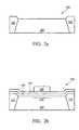
- the strained channel transistor 10includes a gate structure 11 having a gate dielectric 14 underlying a gate electrode 16 .
- the gate structure 11also includes spacers 18 formed along the sidewalls of the gate electrode 16 and the gate dielectric 14 .
- a material having a different lattice constantis formed in recessed regions 20 . Because the material in the recessed regions 20 have a different lattice constant, a lattice mismatch occurs and induces a strain in the region of the substrate positioned between the recessed regions 20 , e.g., the channel region. Ion implants may be performed to form lightly-doped drains 24 and heavily-doped source/drain regions 22 .
- the recessed regions 20may be formed in the LDD 24 and the heavily-doped source/drain regions 22 as illustrated in FIG. 1 a .
- Other attemptsform the recessed regions 20 in the heavily-doped source/drain regions 22 as illustrated in FIG. 1 b .
- Yet other attemptsmay utilize dummy spacers to position the recessed regions under a portion of the spacers 18 .
- the recessed regions 20are typically formed by a silicon etching step performed after the gate dielectric 14 and the gate electrode 16 have been formed. After the silicon etching step is performed, a material having a lattice mismatch with the underlying substrate is grown. Silicon germanium is frequently used to form the recessed regions when a silicon substrate is used. Exposing the gate structure 11 to the silicon etching steps may damage the gate structure 11 and adversely affect the performance of the transistor.
- some attemptsperform the silicon etching steps after the formation of the spacers 18 .
- the silicon etching processmay also erode the spacers 18 , as illustrated by the spacers being etched below the top of the gate electrode 16 in FIG. 1 b .
- the eroded thickness and height of spacers 18 after the silicon etch back stepprovide less protection and isolation to the gate structure 11 and may expose the gate electrode 16 to cracks 25 ( FIG. 1 b ) in an overlying dielectric layer (not shown), such as an etch stop layer or an inter-level dielectric layer, possibly leading to short-circuiting and transistor malfunction.
- the gate structure 11may also be exposed to a hydrofluoric acid or other cleaning solutions applied during a pre-cleaning process performed before depositing the lattice mismatch material.
- the pre-cleaning processmay result in spacer voids 28 , shown in FIG. 1 b , wherein the oxide liner 32 below the spacers 18 is partially etched.
- the spacer voidsmay cause silicide formation under the spacers and may cause the spacer to peel.
- the pre-bake stepmay include heating the wafer to 850° C. or more for five minutes or more before the lattice mismatch material is deposited. This pre-bake step lowers the thermal budget available for LDD implant annealing, source/drain implant annealing, and other manufacturing steps requiring high temperatures, thereby unnecessarily imposing restrictions on other processing steps.
- FIG. 1 balso illustrates a mushroom-like shape 30 that may be formed over the gate structure 11 .
- the mushroom-like shape 30is a common and undesired result of exposing the gate structure 11 to the SiGe deposition step.
- the mushroom-like shape 30may adversely affect the characteristics of the transistor.
- a strained channel transistor formed on a substrate comprising a first materialis provided.
- a source region and a drain regionare formed by creating recessed regions in the substrate prior to forming the gate electrode of the transistor.
- a stress-inducing materialis formed in the recessed regions.
- a cap layermay be formed over the stress-inducing material, and a silicide region may be formed in the source and drain regions.
- a method of forming a strained channel deviceis provided.
- Masking layersare formed and patterned on a substrate to define source and drain regions. Recessed areas are then formed in the substrate, and a stress-inducing material is formed source and drain regions.
- a cap layermay be formed over the stress-inducing material.
- a gate electrode and spacersmay then be formed. The source and drain regions may be silicided.
- FIG. 1 ais a cross-sectional view of a strained channel transistor known in the art
- FIG. 1 bshows gate structure degradation suffered during strained channel formation steps
- FIGS. 2 a - 2 hshow a method of forming a strained channel transistor in accordance with a first illustrative embodiment of the present invention.
- the present inventionrelates to the field of semiconductor devices and, more specifically, to the manufacture of strained channel field effect transistors with lattice-mismatched regions.
- a method of manufacturing in accordance with a first illustrative embodiment of the present inventionis described below.
- FIG. 2 ashows a substrate 100 having an active area 102 defined by shallow trench isolation structures 101 .
- isolation structuressuch as LOCOS and mesa isolation structures, may isolate the active area 102 .
- the substrate 100may comprise any semiconductor material and may comprise known structures including a graded layer or a buried oxide, for example.
- the substrate 100comprises bulk silicon that may be undoped or doped (e.g., p-type, n-type, or a combination thereof). Other materials that are suitable for strained channel transistor formation may be used.
- FIG. 2 bshows the substrate 100 after a first dielectric layer 103 , a second dielectric layer 104 , and a photoresist mask 106 have been formed thereon.
- the first dielectric layer 103may be, for example, a dielectric antireflective coating (DARC)
- the second dielectric layer 104may be, for example, a bottom antireflective coating material (BARC).
- a photoresist mask 106may be formed by depositing and patterning a photoresist material in accordance with standard photolithography techniques. In the embodiment illustrated in FIG. 2 b , the photoresist mask 106 is patterned over a portion of the active area 102 that is to become a strained portion 108 of the substrate 100 .
- the substrate 100 of FIG. 2 bis shown after etching steps have been performed to remove exposed portions of the first dielectric layer 103 and the second dielectric layer 104 and to etch back the substrate, thereby forming recessed areas 112 .
- a channel region 109Positioned between the recessed areas 112 is a channel region 109 .
- a plasma ashing stepmay be used to remove the remaining photoresist mask 106 and the second dielectric layer 104 .
- the depth of the recessed areas 112is about 150 ⁇ to about 2,000 ⁇ .
- a pre-cleaning process stepbe performed after performing the substrate etch back process described above.
- the pre-cleaning processmay be performed with a wet dip in a solution of hydrofluoric acid. It should be noted, however, that performing this pre-cleaning process may cause a step feature 107 to be formed along the side of the STIs 101 . This may be caused because the cleaning solution may remove a portion of the STIs 101 .
- FIG. 2 dshows the epitaxial growth of a stress-inducing layer 114 , such as silicon germanium, followed by the growth of semiconductor layer 116 in the recessed areas 112 .
- the semiconductor layer 116may be formed of silicon, for example.
- the channel region 109preferably comprises silicon and the recessed areas 112 preferably comprise silicon germanium, the channel region 109 and the recessed areas 112 may comprise any material combination that provides any type of strain (e.g., compressive, tensile, uniaxial, or biaxial) in the channel region 109 suitable for a particular application.
- the recessed areas 112may comprise silicon carbon or silicon germanium carbon and the channel region 109 may comprise silicon.
- mismatched recess areas 112may have any shape, including being directly adjacent the channel region 109 , being separated from the adjacent STI 101 , and being in the deep source/drain regions or in the lightly doped drain regions, for example.
- the stress-inducing layer 114is about 150 ⁇ to about 2,200 ⁇ in thickness, and the channel region is about 20 nm to about 150 nm.
- the dielectric layer 118which will be patterned to form a gate dielectric layer in a subsequent step, is preferably an oxide layer formed by any oxidation process, such as wet or dry thermal oxidation in an ambient comprising an oxide, H 2 O, NO, or a combination thereof, or by chemical vapor deposition (CVD) techniques using tetra-ethyl-ortho-silicate (TEOS) and oxygen as a precursor.
- the dielectric layer 118is silicon dioxide material formed by an oxidation process.
- Other materials suitable for strained channel transistor operationmay be used. For example, high-k materials such as hafnium oxide, zirconium oxide, or the like may be used.
- the conductive layer 120which will be patterned to form a gate electrode in subsequent steps, preferably comprises a semiconductor material such as polysilicon, amorphous silicon, or the like.
- the conductive layer 120may be deposited doped or undoped.
- the conductive layer 120comprises polysilicon deposited undoped by low-pressure chemical vapor deposition (LPCVD).
- LPCVDlow-pressure chemical vapor deposition
- the polysiliconmay be doped with, for example, phosphorous ions (or other P-type dopants) to form a PMOS device or boron (or other N-type dopants) to form an NMOS device.
- the polysiliconmay also be deposited, for example, by furnace deposition of an in-situ doped polysilicon.
- the conductive layer 120may comprise a polysilicon metal alloy or a metal gate comprising metals such as tungsten, nickel, and titanium, for example. Additionally, the dielectric layer 118 and the conductive layer 120 may each comprise a single layer or a plurality of layers.
- a gate electrode 119 and a gate dielectric layer 117are patterned over the channel region 109 from the conductive layer 120 ( FIG. 2 f ) and the dielectric layer 118 ( FIG. 2 f ), respectively.
- the dielectric layer 118 and the conductive layer 120may be patterned by depositing and patterning a photoresist material in accordance with photolithography techniques.
- a lightly doped drain (LDD) 130may be formed along the top portion of the substrate 102 by performing an ion implant step and a subsequent anneal.
- the use of a separate mask to form the recessed regions 112 ( FIG. 2 f ) and the gate electrode 119allows the location and size of the recessed regions 112 and the gate electrode 119 to be independently controlled without the use of dummy spacers.
- FIG. 2 hillustrates the substrate 100 after spacers 122 have been formed alongside the gate electrode 119 .
- the spacers 122may be formed by depositing a substantially uniform layer of a dielectric material and performing an anisotropic etch procedure.
- the spacers 122may be formed of silicon nitride, silicon oxynitride, TEOS, or the like.
- Heavily doped source/drain regions 152may be formed by performing an ion implant in which the spacers 122 and the gate electrode 119 act as masks. An annealing process may be performed after the ion implant. It should be noted that the depth of the source/drain regions 152 and the LDDs 130 may vary relative to the recessed regions 112 and that the illustrated depth of the source/drain regions 152 and the LDDs 130 is only provided as one example of an embodiment of the present invention.
- a top portion of the substrate 100 in the source/drain regions and the top portion of the gate electrodemay be silicided to create silicide regions 124 in the source/drain regions 152 and the gate electrode 119 .
- the silicide regions 124may be performed by forming a thin layer of metal, such as titanium or the like, over the wafer.
- a thermal processsuch as an anneal, a rapid thermal process, or the like, causes the metal to react with the exposed silicon, e.g., the exposed silicon of semiconductor layer 116 and the exposed polysilicon of the gate electrode 119 , thereby forming silicide regions 124 . Thereafter, the unreacted metal may be removed.
- embodiments of the present inventionmay be easily and cost effectively incorporated into current semiconductor fabrication processes.
- the integrity of the gate structures of the strained channel devicesis preserved.
- gate structure damagesuch as mushroom-like gate head formation, spacer erosion, spacer cracking, and spacer void formation may be prevented or reduced.
Landscapes
- Insulated Gate Type Field-Effect Transistor (AREA)
Abstract
Description
Claims (21)
Priority Applications (3)
| Application Number | Priority Date | Filing Date | Title |
|---|---|---|---|
| US10/897,563US7867860B2 (en) | 2003-07-25 | 2004-07-23 | Strained channel transistor formation |
| TW94124926ATWI279915B (en) | 2004-07-23 | 2005-07-22 | A transistor and a method for forming a strained channel device |
| CNB2005100852731ACN100401530C (en) | 2004-07-23 | 2005-07-22 | Method for forming strained channel element |
Applications Claiming Priority (2)
| Application Number | Priority Date | Filing Date | Title |
|---|---|---|---|
| US49042503P | 2003-07-25 | 2003-07-25 | |
| US10/897,563US7867860B2 (en) | 2003-07-25 | 2004-07-23 | Strained channel transistor formation |
Publications (2)
| Publication Number | Publication Date |
|---|---|
| US20050082522A1 US20050082522A1 (en) | 2005-04-21 |
| US7867860B2true US7867860B2 (en) | 2011-01-11 |
Family
ID=36082957
Family Applications (2)
| Application Number | Title | Priority Date | Filing Date |
|---|---|---|---|
| US10/655,255Expired - LifetimeUS7078742B2 (en) | 2003-07-25 | 2003-09-04 | Strained-channel semiconductor structure and method of fabricating the same |
| US10/897,563Active2026-10-14US7867860B2 (en) | 2003-07-25 | 2004-07-23 | Strained channel transistor formation |
Family Applications Before (1)
| Application Number | Title | Priority Date | Filing Date |
|---|---|---|---|
| US10/655,255Expired - LifetimeUS7078742B2 (en) | 2003-07-25 | 2003-09-04 | Strained-channel semiconductor structure and method of fabricating the same |
Country Status (3)
| Country | Link |
|---|---|
| US (2) | US7078742B2 (en) |
| CN (1) | CN2760759Y (en) |
| TW (1) | TWI253752B (en) |
Cited By (8)
| Publication number | Priority date | Publication date | Assignee | Title |
|---|---|---|---|---|
| US20090026497A1 (en)* | 2005-07-05 | 2009-01-29 | Nissan Motor Co., Ltd. | Method for Producing Semiconductor Device |
| US20110272738A1 (en)* | 2004-07-27 | 2011-11-10 | Chang-Woo Oh | Semiconductor Devices Including Fin Shaped Semiconductor Regions and Stress Inducing Layers |
| WO2014047258A1 (en)* | 2012-09-19 | 2014-03-27 | International Business Machines Corporation | Semiconductor device and method with greater epitaxial growth on 110 crystal plane |
| US9041062B2 (en) | 2013-09-19 | 2015-05-26 | International Business Machines Corporation | Silicon-on-nothing FinFETs |
| US9608117B2 (en) | 2015-03-30 | 2017-03-28 | Samsung Electronics Co., Ltd. | Semiconductor devices including a finFET |
| US9899274B2 (en) | 2015-03-16 | 2018-02-20 | International Business Machines Corporation | Low-cost SOI FinFET technology |
| US11450768B2 (en) | 2020-10-05 | 2022-09-20 | Sandisk Technologies Llc | High voltage field effect transistor with vertical current paths and method of making the same |
| US11978774B2 (en) | 2020-10-05 | 2024-05-07 | Sandisk Technologies Llc | High voltage field effect transistor with vertical current paths and method of making the same |
Families Citing this family (78)
| Publication number | Priority date | Publication date | Assignee | Title |
|---|---|---|---|---|
| US7112485B2 (en)* | 2002-08-28 | 2006-09-26 | Micron Technology, Inc. | Systems and methods for forming zirconium and/or hafnium-containing layers |
| CN100446272C (en)* | 2003-09-04 | 2008-12-24 | 台湾积体电路制造股份有限公司 | strained channel semiconductor structure |
| US7303949B2 (en)* | 2003-10-20 | 2007-12-04 | International Business Machines Corporation | High performance stress-enhanced MOSFETs using Si:C and SiGe epitaxial source/drain and method of manufacture |
| US7183221B2 (en)* | 2003-11-06 | 2007-02-27 | Texas Instruments Incorporated | Method of fabricating a semiconductor having dual gate electrodes using a composition-altered metal layer |
| KR100519800B1 (en)* | 2004-01-13 | 2005-10-10 | 삼성전자주식회사 | method of fabricating Lanthanum oxide layer and method of fabricating MOSFET transistor and capacitor using the same |
| US7205206B2 (en)* | 2004-03-03 | 2007-04-17 | International Business Machines Corporation | Method of fabricating mobility enhanced CMOS devices |
| JP2005286341A (en) | 2004-03-30 | 2005-10-13 | Samsung Electronics Co Ltd | Low noise and high performance LSI device, layout and manufacturing method thereof |
| TWI463526B (en)* | 2004-06-24 | 2014-12-01 | Ibm | Method for improving stress-induced CMOS components and components prepared by the method |
| US7227205B2 (en)* | 2004-06-24 | 2007-06-05 | International Business Machines Corporation | Strained-silicon CMOS device and method |
| US7598134B2 (en)* | 2004-07-28 | 2009-10-06 | Micron Technology, Inc. | Memory device forming methods |
| US7161199B2 (en)* | 2004-08-24 | 2007-01-09 | Freescale Semiconductor, Inc. | Transistor structure with stress modification and capacitive reduction feature in a width direction and method thereof |
| US7268399B2 (en)* | 2004-08-31 | 2007-09-11 | Texas Instruments Incorporated | Enhanced PMOS via transverse stress |
| JP2006165081A (en)* | 2004-12-03 | 2006-06-22 | Fujitsu Ltd | Semiconductor device manufacturing method and semiconductor device |
| CA2589539A1 (en)* | 2004-12-07 | 2006-06-15 | Thunderbird Technologies, Inc. | Strained silicon, gate engineered fermi-fets |
| US7732289B2 (en)* | 2005-07-05 | 2010-06-08 | Taiwan Semiconductor Manufacturing Company, Ltd. | Method of forming a MOS device with an additional layer |
| US8003470B2 (en) | 2005-09-13 | 2011-08-23 | Infineon Technologies Ag | Strained semiconductor device and method of making the same |
| TW200713455A (en)* | 2005-09-20 | 2007-04-01 | Applied Materials Inc | Method to form a device on a SOI substrate |
| DE102005052055B3 (en)* | 2005-10-31 | 2007-04-26 | Advanced Micro Devices, Inc., Sunnyvale | Transistor and semiconductor components and production process for thin film silicon on insulator transistor has embedded deformed layer |
| US8407634B1 (en) | 2005-12-01 | 2013-03-26 | Synopsys Inc. | Analysis of stress impact on transistor performance |
| CN100411146C (en)* | 2005-12-06 | 2008-08-13 | 联华电子股份有限公司 | Method for manufacturing strained silicon complementary metal oxide semiconductor transistor |
| US7656049B2 (en) | 2005-12-22 | 2010-02-02 | Micron Technology, Inc. | CMOS device with asymmetric gate strain |
| US7525160B2 (en)* | 2005-12-27 | 2009-04-28 | Intel Corporation | Multigate device with recessed strain regions |
| US8900980B2 (en)* | 2006-01-20 | 2014-12-02 | Taiwan Semiconductor Manufacturing Company, Ltd. | Defect-free SiGe source/drain formation by epitaxy-free process |
| JP2007200972A (en)* | 2006-01-24 | 2007-08-09 | Nec Electronics Corp | Semiconductor device and manufacturing method thereof |
| US8441000B2 (en)* | 2006-02-01 | 2013-05-14 | International Business Machines Corporation | Heterojunction tunneling field effect transistors, and methods for fabricating the same |
| US7544584B2 (en)* | 2006-02-16 | 2009-06-09 | Micron Technology, Inc. | Localized compressive strained semiconductor |
| US7696019B2 (en)* | 2006-03-09 | 2010-04-13 | Infineon Technologies Ag | Semiconductor devices and methods of manufacturing thereof |
| US8017487B2 (en)* | 2006-04-05 | 2011-09-13 | Globalfoundries Singapore Pte. Ltd. | Method to control source/drain stressor profiles for stress engineering |
| US8076189B2 (en) | 2006-04-11 | 2011-12-13 | Freescale Semiconductor, Inc. | Method of forming a semiconductor device and semiconductor device |
| DE102006019937B4 (en)* | 2006-04-28 | 2010-11-25 | Advanced Micro Devices, Inc., Sunnyvale | Method for producing an SOI transistor with embedded deformation layer and a reduced effect of the potential-free body |
| US7618866B2 (en)* | 2006-06-09 | 2009-11-17 | International Business Machines Corporation | Structure and method to form multilayer embedded stressors |
| KR100732318B1 (en)* | 2006-06-30 | 2007-06-25 | 주식회사 하이닉스반도체 | Nonvolatile Memory Device and Manufacturing Method Thereof |
| DE102006035665B4 (en)* | 2006-07-31 | 2010-12-09 | Advanced Micro Devices, Inc., Sunnyvale | Method for producing a field effect transistor and field effect transistor |
| US7485544B2 (en) | 2006-08-02 | 2009-02-03 | Micron Technology, Inc. | Strained semiconductor, devices and systems and methods of formation |
| US8962447B2 (en)* | 2006-08-03 | 2015-02-24 | Micron Technology, Inc. | Bonded strained semiconductor with a desired surface orientation and conductance direction |
| US7968960B2 (en) | 2006-08-18 | 2011-06-28 | Micron Technology, Inc. | Methods of forming strained semiconductor channels |
| US20080042123A1 (en)* | 2006-08-18 | 2008-02-21 | Kong-Beng Thei | Methods for controlling thickness uniformity of SiGe regions |
| CN100530654C (en)* | 2006-08-18 | 2009-08-19 | 台湾积体电路制造股份有限公司 | Integrated circuit and mask set for forming integrated circuit |
| US7612364B2 (en)* | 2006-08-30 | 2009-11-03 | Taiwan Semiconductor Manufacturing Company, Ltd. | MOS devices with source/drain regions having stressed regions and non-stressed regions |
| US7554110B2 (en)* | 2006-09-15 | 2009-06-30 | Taiwan Semiconductor Manufacturing Company, Ltd. | MOS devices with partial stressor channel |
| US8008157B2 (en)* | 2006-10-27 | 2011-08-30 | Taiwan Semiconductor Manufacturing Company, Ltd. | CMOS device with raised source and drain regions |
| US7750338B2 (en)* | 2006-12-05 | 2010-07-06 | Taiwan Semiconductor Manufacturing Company, Ltd. | Dual-SiGe epitaxy for MOS devices |
| EP1936696A1 (en)* | 2006-12-22 | 2008-06-25 | INTERUNIVERSITAIR MICROELEKTRONICA CENTRUM vzw (IMEC) | A field effect transistor device and methods of production thereof |
| US8217423B2 (en)* | 2007-01-04 | 2012-07-10 | International Business Machines Corporation | Structure and method for mobility enhanced MOSFETs with unalloyed silicide |
| US8558278B2 (en)* | 2007-01-16 | 2013-10-15 | Taiwan Semiconductor Manufacturing Company, Ltd. | Strained transistor with optimized drive current and method of forming |
| DE102007004862B4 (en)* | 2007-01-31 | 2014-01-30 | Globalfoundries Inc. | A method of fabricating Si-Ge containing drain / source regions in lower Si / Ge loss transistors |
| US8569837B2 (en)* | 2007-05-07 | 2013-10-29 | Taiwan Semiconductor Manufacturing Company, Ltd. | MOS devices having elevated source/drain regions |
| US8450165B2 (en) | 2007-05-14 | 2013-05-28 | Intel Corporation | Semiconductor device having tipless epitaxial source/drain regions |
| US7816686B2 (en)* | 2007-06-12 | 2010-10-19 | Taiwan Semiconductor Manufacturing Company, Ltd. | Forming silicides with reduced tailing on silicon germanium and silicon |
| JP5286701B2 (en) | 2007-06-27 | 2013-09-11 | ソニー株式会社 | Semiconductor device and manufacturing method of semiconductor device |
| US8115254B2 (en) | 2007-09-25 | 2012-02-14 | International Business Machines Corporation | Semiconductor-on-insulator structures including a trench containing an insulator stressor plug and method of fabricating same |
| US8288233B2 (en)* | 2007-09-28 | 2012-10-16 | Intel Corporation | Method to introduce uniaxial strain in multigate nanoscale transistors by self aligned SI to SIGE conversion processes and structures formed thereby |
| JP5389346B2 (en)* | 2007-10-11 | 2014-01-15 | 富士通セミコンダクター株式会社 | MOS field effect transistor and manufacturing method thereof |
| US8492846B2 (en) | 2007-11-15 | 2013-07-23 | International Business Machines Corporation | Stress-generating shallow trench isolation structure having dual composition |
| US20090184341A1 (en)* | 2008-01-17 | 2009-07-23 | Chartered Semiconductor Manufacturing, Ltd. | Elimination of STI recess and facet growth in embedded silicon-germanium (eSiGe) module |
| US8115194B2 (en)* | 2008-02-21 | 2012-02-14 | United Microelectronics Corp. | Semiconductor device capable of providing identical strains to each channel region of the transistors |
| US20090224328A1 (en)* | 2008-03-04 | 2009-09-10 | Shyh-Fann Ting | Semiconductor device |
| US7943961B2 (en)* | 2008-03-13 | 2011-05-17 | Taiwan Semiconductor Manufacturing Company, Ltd. | Strain bars in stressed layers of MOS devices |
| US7808051B2 (en)* | 2008-09-29 | 2010-10-05 | Taiwan Semiconductor Manufacturing Company, Ltd. | Standard cell without OD space effect in Y-direction |
| US8253200B2 (en) | 2008-11-19 | 2012-08-28 | Omnivision Technologies, Inc. | Lightly-doped drains (LDD) of image sensor transistors using selective epitaxy |
| US8232171B2 (en)* | 2009-09-17 | 2012-07-31 | International Business Machines Corporation | Structure with isotropic silicon recess profile in nanoscale dimensions |
| TWI406362B (en)* | 2009-11-19 | 2013-08-21 | Univ Nat United | A complementary gold - oxygen - semi - crystal system method for increasing the mobility of holes in PMOS element region |
| US8598003B2 (en) | 2009-12-21 | 2013-12-03 | Intel Corporation | Semiconductor device having doped epitaxial region and its methods of fabrication |
| US8236660B2 (en) | 2010-04-21 | 2012-08-07 | International Business Machines Corporation | Monolayer dopant embedded stressor for advanced CMOS |
| US8299535B2 (en)* | 2010-06-25 | 2012-10-30 | International Business Machines Corporation | Delta monolayer dopants epitaxy for embedded source/drain silicide |
| US8629426B2 (en)* | 2010-12-03 | 2014-01-14 | Taiwan Semiconductor Manufacturing Company, Ltd. | Source/drain stressor having enhanced carrier mobility manufacturing same |
| DE102011076695B4 (en)* | 2011-05-30 | 2013-05-08 | Globalfoundries Inc. | Embedded strain inducing material transistors formed in cavities formed by an oxidation etch process |
| US9817928B2 (en) | 2012-08-31 | 2017-11-14 | Synopsys, Inc. | Latch-up suppression and substrate noise coupling reduction through a substrate back-tie for 3D integrated circuits |
| US9190346B2 (en) | 2012-08-31 | 2015-11-17 | Synopsys, Inc. | Latch-up suppression and substrate noise coupling reduction through a substrate back-tie for 3D integrated circuits |
| CN103779223B (en)* | 2012-10-23 | 2016-07-06 | 中国科学院微电子研究所 | MOSFET manufacturing method |
| US8847324B2 (en) | 2012-12-17 | 2014-09-30 | Synopsys, Inc. | Increasing ION /IOFF ratio in FinFETs and nano-wires |
| US9379018B2 (en) | 2012-12-17 | 2016-06-28 | Synopsys, Inc. | Increasing Ion/Ioff ratio in FinFETs and nano-wires |
| US9299837B2 (en)* | 2013-05-22 | 2016-03-29 | Globalfoundries Inc. | Integrated circuit having MOSFET with embedded stressor and method to fabricate same |
| US9691898B2 (en)* | 2013-12-19 | 2017-06-27 | Taiwan Semiconductor Manufacturing Co., Ltd. | Germanium profile for channel strain |
| US9287398B2 (en) | 2014-02-14 | 2016-03-15 | Taiwan Semiconductor Manufacturing Co., Ltd. | Transistor strain-inducing scheme |
| US9450079B2 (en) | 2014-04-09 | 2016-09-20 | International Business Machines Corporation | FinFET having highly doped source and drain regions |
| US9793407B2 (en)* | 2015-12-15 | 2017-10-17 | Taiwan Semiconductor Manufacturing Co., Ltd. | Fin field effect transistor |
| WO2017111806A1 (en)* | 2015-12-24 | 2017-06-29 | Intel Corporation | Methods of forming doped source/drain contacts and structures formed thereby |
Citations (151)
| Publication number | Priority date | Publication date | Assignee | Title |
|---|---|---|---|---|
| US4069094A (en) | 1976-12-30 | 1978-01-17 | Rca Corporation | Method of manufacturing apertured aluminum oxide substrates |
| US4314269A (en) | 1978-06-06 | 1982-02-02 | Vlsi Technology Research Association | Semiconductor resistor comprising a resistor layer along a side surface |
| US4497683A (en) | 1982-05-03 | 1985-02-05 | At&T Bell Laboratories | Process for producing dielectrically isolated silicon devices |
| US4631803A (en) | 1985-02-14 | 1986-12-30 | Texas Instruments Incorporated | Method of fabricating defect free trench isolation devices |
| US4892614A (en)* | 1986-07-07 | 1990-01-09 | Texas Instruments Incorporated | Integrated circuit isolation process |
| US4946799A (en) | 1988-07-08 | 1990-08-07 | Texas Instruments, Incorporated | Process for making high performance silicon-on-insulator transistor with body node to source node connection |
| US4952993A (en)* | 1987-07-16 | 1990-08-28 | Kabushiki Kaisha Toshiba | Semiconductor device and manufacturing method thereof |
| US5130773A (en) | 1989-06-30 | 1992-07-14 | Hitachi, Ltd. | Semiconductor device with photosensitivity |
| US5155571A (en) | 1990-08-06 | 1992-10-13 | The Regents Of The University Of California | Complementary field effect transistors having strained superlattice structure |
| US5273915A (en) | 1992-10-05 | 1993-12-28 | Motorola, Inc. | Method for fabricating bipolar junction and MOS transistors on SOI |
| US5338960A (en) | 1992-08-05 | 1994-08-16 | Harris Corporation | Formation of dual polarity source/drain extensions in lateral complementary channel MOS architectures |
| US5378919A (en) | 1991-01-21 | 1995-01-03 | Sony Corporation | Semiconductor integrated circuit device with plural gates and plural passive devices |
| US5447884A (en) | 1994-06-29 | 1995-09-05 | International Business Machines Corporation | Shallow trench isolation with thin nitride liner |
| US5461250A (en) | 1992-08-10 | 1995-10-24 | International Business Machines Corporation | SiGe thin film or SOI MOSFET and method for making the same |
| EP0683522A2 (en) | 1994-05-20 | 1995-11-22 | International Business Machines Corporation | CMOS with strained Si/SiGe layers |
| US5479033A (en) | 1994-05-27 | 1995-12-26 | Sandia Corporation | Complementary junction heterostructure field-effect transistor |
| US5525828A (en) | 1991-10-31 | 1996-06-11 | International Business Machines Corporation | High speed silicon-based lateral junction photodetectors having recessed electrodes and thick oxide to reduce fringing fields |
| US5596529A (en) | 1993-11-30 | 1997-01-21 | Kabushiki Kaisha Toshiba | Nonvolatile semiconductor memory device |
| US5607865A (en) | 1995-01-27 | 1997-03-04 | Goldstar Electron Co., Ltd. | Structure and fabrication method for a thin film transistor |
| US5629544A (en) | 1995-04-25 | 1997-05-13 | International Business Machines Corporation | Semiconductor diode with silicide films and trench isolation |
| US5656524A (en) | 1994-05-06 | 1997-08-12 | Texas Instruments Incorporated | Method of forming a polysilicon resistor using an oxide, nitride stack |
| US5708288A (en) | 1995-11-02 | 1998-01-13 | Motorola, Inc. | Thin film silicon on insulator semiconductor integrated circuit with electrostatic damage protection and method |
| US5714777A (en) | 1997-02-19 | 1998-02-03 | International Business Machines Corporation | Si/SiGe vertical junction field effect transistor |
| EP0828296A2 (en) | 1996-09-03 | 1998-03-11 | International Business Machines Corporation | High temperature superconductivity in strained Si/SiGe |
| US5763315A (en) | 1997-01-28 | 1998-06-09 | International Business Machines Corporation | Shallow trench isolation with oxide-nitride/oxynitride liner |
| US5770881A (en) | 1996-09-12 | 1998-06-23 | International Business Machines Coproration | SOI FET design to reduce transient bipolar current |
| US5789807A (en) | 1996-10-15 | 1998-08-04 | International Business Machines Corporation | On-chip power distribution for improved decoupling |
| US5811857A (en) | 1996-10-22 | 1998-09-22 | International Business Machines Corporation | Silicon-on-insulator body-coupled gated diode for electrostatic discharge (ESD) and analog applications |
| US5955766A (en) | 1995-06-12 | 1999-09-21 | Kabushiki Kaisha Toshiba | Diode with controlled breakdown |
| US5965917A (en) | 1999-01-04 | 1999-10-12 | Advanced Micro Devices, Inc. | Structure and method of formation of body contacts in SOI MOSFETS to elimate floating body effects |
| US5972722A (en) | 1998-04-14 | 1999-10-26 | Texas Instruments Incorporated | Adhesion promoting sacrificial etch stop layer in advanced capacitor structures |
| US6008095A (en) | 1998-08-07 | 1999-12-28 | Advanced Micro Devices, Inc. | Process for formation of isolation trenches with high-K gate dielectrics |
| US6015993A (en) | 1998-08-31 | 2000-01-18 | International Business Machines Corporation | Semiconductor diode with depleted polysilicon gate structure and method |
| US6015990A (en) | 1997-02-27 | 2000-01-18 | Kabushiki Kaisha Toshiba | Semiconductor memory device and method of manufacturing the same |
| US6027988A (en) | 1997-05-28 | 2000-02-22 | The Regents Of The University Of California | Method of separating films from bulk substrates by plasma immersion ion implantation |
| US6040991A (en) | 1999-01-04 | 2000-03-21 | International Business Machines Corporation | SRAM memory cell having reduced surface area |
| US6061267A (en) | 1998-09-28 | 2000-05-09 | Texas Instruments Incorporated | Memory circuits, systems, and methods with cells using back bias to control the threshold voltage of one or more corresponding cell transistors |
| US6059895A (en) | 1997-04-30 | 2000-05-09 | International Business Machines Corporation | Strained Si/SiGe layers on insulator |
| US6096591A (en) | 1997-06-30 | 2000-08-01 | Advanced Micro Devices, Inc. | Method of making an IGFET and a protected resistor with reduced processing steps |
| US6100153A (en) | 1998-01-20 | 2000-08-08 | International Business Machines Corporation | Reliable diffusion resistor and diffusion capacitor |
| US6100204A (en) | 1998-07-28 | 2000-08-08 | Advanced Micro Devices, Inc. | Method of making ultra thin gate oxide using aluminum oxide |
| US6103599A (en) | 1997-07-25 | 2000-08-15 | Silicon Genesis Corporation | Planarizing technique for multilayered substrates |
| US6107125A (en) | 1997-06-18 | 2000-08-22 | International Business Machines Corporation | SOI/bulk hybrid substrate and method of forming the same |
| US6111267A (en) | 1997-05-13 | 2000-08-29 | Siemens Aktiengesellschaft | CMOS integrated circuit including forming doped wells, a layer of intrinsic silicon, a stressed silicon germanium layer where germanium is between 25 and 50%, and another intrinsic silicon layer |
| US6190996B1 (en) | 1997-11-12 | 2001-02-20 | Micron Technology, Inc. | Method of making an insulator for electrical structures |
| US6198173B1 (en) | 1997-10-27 | 2001-03-06 | Taiwan Semiconductor Manufacturing Company | SRAM with improved Beta ratio |
| US6222234B1 (en) | 1998-04-15 | 2001-04-24 | Nec Corporation | Semiconductor device having partially and fully depleted SOI elements on a common substrate |
| US6256239B1 (en) | 1998-10-27 | 2001-07-03 | Fujitsu Limited | Redundant decision circuit for semiconductor memory device |
| US6258664B1 (en) | 1999-02-16 | 2001-07-10 | Micron Technology, Inc. | Methods of forming silicon-comprising materials having roughened outer surfaces, and methods of forming capacitor constructions |
| US6281059B1 (en) | 2000-05-11 | 2001-08-28 | Worldwide Semiconductor Manufacturing Corp. | Method of doing ESD protective device ion implant without additional photo mask |
| US6291321B1 (en) | 1997-06-24 | 2001-09-18 | Massachusetts Institute Of Technology | Controlling threading dislocation densities in Ge on Si using graded GeSi layers and planarization |
| US6294834B1 (en) | 2000-01-21 | 2001-09-25 | United Microelectronics Corp. | Structure of combined passive elements and logic circuit on a silicon on insulator wafer |
| US20010028089A1 (en) | 2000-04-04 | 2001-10-11 | Adan Alberto O. | Semiconductor device of SOI structure |
| US6303479B1 (en) | 1999-12-16 | 2001-10-16 | Spinnaker Semiconductor, Inc. | Method of manufacturing a short-channel FET with Schottky-barrier source and drain contacts |
| US6339232B1 (en) | 1999-09-20 | 2002-01-15 | Kabushika Kaisha Toshiba | Semiconductor device |
| US6341083B1 (en) | 2000-11-13 | 2002-01-22 | International Business Machines Corporation | CMOS SRAM cell with PFET passgate devices |
| US20020008289A1 (en) | 2000-07-24 | 2002-01-24 | Junichi Murota | Mosfet with strained channel layer |
| US6342410B1 (en) | 2000-07-10 | 2002-01-29 | Advanced Micro Devices, Inc. | Fabrication of a field effect transistor with three sided gate structure on semiconductor on insulator |
| US20020031890A1 (en) | 2000-08-28 | 2002-03-14 | Takayuki Watanabe | Semiconductor device of STI structure and method of fabricating MOS transistors having consistent threshold voltages |
| US6358791B1 (en) | 1999-06-04 | 2002-03-19 | International Business Machines Corporation | Method for increasing a very-large-scale-integrated (VLSI) capacitor size on bulk silicon and silicon-on-insulator (SOI) wafers and structure formed thereby |
| US20020045318A1 (en) | 1999-04-09 | 2002-04-18 | Coming Chen | Method for manufacturing mos transistor |
| US6387739B1 (en) | 1998-08-07 | 2002-05-14 | International Business Machines Corporation | Method and improved SOI body contact structure for transistors |
| US6407406B1 (en) | 1998-06-30 | 2002-06-18 | Kabushiki Kaisha Toshiba | Semiconductor device and method of manufacturing the same |
| US20020074598A1 (en) | 1999-06-28 | 2002-06-20 | Doyle Brian S. | Methodology for control of short channel effects in MOS transistors |
| US20020076899A1 (en) | 2000-08-02 | 2002-06-20 | Stmicroelectronics S.A. | Process for fabricating a substrate of the silicon-on-insulator or silicon-on-nothing type and resulting device |
| US6413802B1 (en) | 2000-10-23 | 2002-07-02 | The Regents Of The University Of California | Finfet transistor structures having a double gate channel extending vertically from a substrate and methods of manufacture |
| US6414355B1 (en) | 2001-01-26 | 2002-07-02 | Advanced Micro Devices, Inc. | Silicon-on-insulator (SOI) chip having an active layer of non-uniform thickness |
| US6420218B1 (en) | 2000-04-24 | 2002-07-16 | Advanced Micro Devices, Inc. | Ultra-thin-body SOI MOS transistors having recessed source and drain regions |
| US6429061B1 (en) | 2000-07-26 | 2002-08-06 | International Business Machines Corporation | Method to fabricate a strained Si CMOS structure using selective epitaxial deposition of Si after device isolation formation |
| US6433382B1 (en) | 1995-04-06 | 2002-08-13 | Motorola, Inc. | Split-gate vertically oriented EEPROM device and process |
| US6448613B1 (en) | 2000-01-07 | 2002-09-10 | Advanced Micro Devices, Inc. | Fabrication of a field effect transistor with minimized parasitic Miller capacitance |
| US20020125471A1 (en) | 2000-12-04 | 2002-09-12 | Fitzgerald Eugene A. | CMOS inverter circuits utilizing strained silicon surface channel MOSFETS |
| US20020153549A1 (en) | 2001-04-20 | 2002-10-24 | Laibowitz Robert Benjamin | Tailored insulator properties for devices |
| US6475869B1 (en) | 2001-02-26 | 2002-11-05 | Advanced Micro Devices, Inc. | Method of forming a double gate transistor having an epitaxial silicon/germanium channel region |
| US6475838B1 (en) | 2000-03-14 | 2002-11-05 | International Business Machines Corporation | Methods for forming decoupling capacitors |
| US20020163036A1 (en) | 2001-05-01 | 2002-11-07 | Mitsubishi Denki Kabushiki Kaisha | Semiconductor Device |
| US6489684B1 (en) | 2001-05-14 | 2002-12-03 | Taiwan Semiconductor Manufacturing Company | Reduction of electromigration in dual damascene connector |
| US6489664B2 (en) | 1997-12-12 | 2002-12-03 | Stmicroelectronics S.R.L. | Process for fabricating integrated multi-crystal silicon resistors in MOS technology, and integrated MOS device comprising multi-crystal silicon resistors |
| US20020190284A1 (en) | 1999-12-30 | 2002-12-19 | Anand Murthy | Novel mos transistor structure and method of fabrication |
| US6498359B2 (en)* | 2000-05-22 | 2002-12-24 | Max-Planck-Gesellschaft Zur Foerderung Der Wissenschaften E.V. | Field-effect transistor based on embedded cluster structures and process for its production |
| US20030001219A1 (en) | 2001-06-29 | 2003-01-02 | Chau Robert S. | Novel transistor structure and method of fabrication |
| US6518610B2 (en) | 2001-02-20 | 2003-02-11 | Micron Technology, Inc. | Rhodium-rich oxygen barriers |
| US20030030091A1 (en) | 2001-08-13 | 2003-02-13 | Amberwave Systems Corporation | Dynamic random access memory trench capacitors |
| US6521952B1 (en) | 2001-10-22 | 2003-02-18 | United Microelectronics Corp. | Method of forming a silicon controlled rectifier devices in SOI CMOS process for on-chip ESD protection |
| US6525403B2 (en) | 2000-09-28 | 2003-02-25 | Kabushiki Kaisha Toshiba | Semiconductor device having MIS field effect transistors or three-dimensional structure |
| US6524905B2 (en) | 2000-07-14 | 2003-02-25 | Nec Corporation | Semiconductor device, and thin film capacitor |
| US6531741B1 (en) | 1999-03-03 | 2003-03-11 | International Business Machines Corporation | Dual buried oxide film SOI structure and method of manufacturing the same |
| US6541343B1 (en)* | 1999-12-30 | 2003-04-01 | Intel Corporation | Methods of making field effect transistor structure with partially isolated source/drain junctions |
| US6549450B1 (en) | 2000-11-08 | 2003-04-15 | Ibm Corporation | Method and system for improving the performance on SOI memory arrays in an SRAM architecture system |
| US20030072126A1 (en) | 2001-08-30 | 2003-04-17 | Micron Technology, Inc. | Decoupling capacitor for high frequency noise immunity |
| US6555839B2 (en) | 2000-05-26 | 2003-04-29 | Amberwave Systems Corporation | Buried channel strained silicon FET using a supply layer created through ion implantation |
| US20030080388A1 (en) | 2001-10-29 | 2003-05-01 | Power Integrations, Inc. | Lateral power mosfet for high switching speeds |
| US20030080386A1 (en) | 2001-02-15 | 2003-05-01 | United Microelectronics Corp. | Silicon-on-insulator diodes and ESD protection circuits |
| US6558998B2 (en) | 1998-06-15 | 2003-05-06 | Marc Belleville | SOI type integrated circuit with a decoupling capacity and process for embodiment of such a circuit |
| US20030089901A1 (en)* | 2001-03-02 | 2003-05-15 | Fitzgerald Eugene A. | Relaxed silicon germanium platform for high speed cmos electronics and high speed analog circuits |
| US6573172B1 (en) | 2002-09-16 | 2003-06-03 | Advanced Micro Devices, Inc. | Methods for improving carrier mobility of PMOS and NMOS devices |
| US6576526B2 (en) | 2001-07-09 | 2003-06-10 | Chartered Semiconductor Manufacturing Ltd. | Darc layer for MIM process integration |
| US6586311B2 (en) | 2001-04-25 | 2003-07-01 | Advanced Micro Devices, Inc. | Salicide block for silicon-on-insulator (SOI) applications |
| US6600170B1 (en) | 2001-12-17 | 2003-07-29 | Advanced Micro Devices, Inc. | CMOS with strained silicon channel NMOS and silicon germanium channel PMOS |
| US6605514B1 (en) | 2002-07-31 | 2003-08-12 | Advanced Micro Devices, Inc. | Planar finFET patterning using amorphous carbon |
| US6611029B1 (en) | 2002-11-08 | 2003-08-26 | Advanced Micro Devices, Inc. | Double gate semiconductor device having separate gates |
| US6617643B1 (en) | 2002-06-28 | 2003-09-09 | Mcnc | Low power tunneling metal-oxide-semiconductor (MOS) device |
| US6621131B2 (en) | 2001-11-01 | 2003-09-16 | Intel Corporation | Semiconductor transistor having a stressed channel |
| US20030183880A1 (en) | 2002-03-27 | 2003-10-02 | Yoshiro Goto | Semiconductor device covering transistor and resistance with capacitor material |
| US6635909B2 (en) | 2002-03-19 | 2003-10-21 | International Business Machines Corporation | Strained fin FETs structure and method |
| US6642090B1 (en) | 2002-06-03 | 2003-11-04 | International Business Machines Corporation | Fin FET devices from bulk semiconductor and method for forming |
| US6657276B1 (en) | 2001-12-10 | 2003-12-02 | Advanced Micro Devices, Inc. | Shallow trench isolation (STI) region with high-K liner and method of formation |
| US6657259B2 (en) | 2001-12-04 | 2003-12-02 | International Business Machines Corporation | Multiple-plane FinFET CMOS |
| US6674100B2 (en) | 1996-09-17 | 2004-01-06 | Matsushita Electric Industrial Co., Ltd. | SiGeC-based CMOSFET with separate heterojunctions |
| US20040007715A1 (en) | 2002-07-09 | 2004-01-15 | Webb Douglas A. | Heterojunction field effect transistors using silicon-germanium and silicon-carbon alloys |
| US20040016972A1 (en) | 2002-07-29 | 2004-01-29 | Dinkar Singh | Enhanced t-gate structure for modulation doped field effect transistors |
| US6686247B1 (en) | 2002-08-22 | 2004-02-03 | Intel Corporation | Self-aligned contacts to gates |
| US6690082B2 (en) | 2001-09-28 | 2004-02-10 | Agere Systems Inc. | High dopant concentration diffused resistor and method of manufacture therefor |
| US20040026765A1 (en) | 2002-06-07 | 2004-02-12 | Amberwave Systems Corporation | Semiconductor devices having strained dual channel layers |
| US20040031979A1 (en) | 2002-06-07 | 2004-02-19 | Amberwave Systems Corporation | Strained-semiconductor-on-insulator device structures |
| US6706576B1 (en) | 2002-03-14 | 2004-03-16 | Advanced Micro Devices, Inc. | Laser thermal annealing of silicon nitride for increased density and etch selectivity |
| US20040061178A1 (en) | 2002-09-30 | 2004-04-01 | Advanced Micro Devices Inc. | Finfet having improved carrier mobility and method of its formation |
| US6720619B1 (en) | 2002-12-13 | 2004-04-13 | Taiwan Semiconductor Manufacturing Company, Ltd. | Semiconductor-on-insulator chip incorporating partially-depleted, fully-depleted, and multiple-gate devices |
| US6724019B2 (en) | 2000-05-25 | 2004-04-20 | Renesas Technology Corporation | Multi-layered, single crystal field effect transistor |
| US20040075122A1 (en) | 2002-10-22 | 2004-04-22 | Ming-Ren Lin | Double and triple gate MOSFET devices and methods for making same |
| US20040087098A1 (en) | 2002-11-01 | 2004-05-06 | Chartered Semiconductor Manufacturing Ltd. | Mim and metal resistor formation at cu beol using only one extra mask |
| US6737710B2 (en)* | 1999-06-30 | 2004-05-18 | Intel Corporation | Transistor structure having silicide source/drain extensions |
| US20040114422A1 (en) | 2002-12-17 | 2004-06-17 | Tomoaki Yabe | SRAM cell and integrated memory circuit using the same |
| US6759717B2 (en) | 1997-06-30 | 2004-07-06 | Stmicroelectronics, Inc. | CMOS integrated circuit device with LDD n-channel transistor and non-LDD p-channel transistor |
| US6762448B1 (en) | 2003-04-03 | 2004-07-13 | Advanced Micro Devices, Inc. | FinFET device with multiple fin structures |
| US6784101B1 (en) | 2002-05-16 | 2004-08-31 | Advanced Micro Devices Inc | Formation of high-k gate dielectric layers for MOS devices fabricated on strained lattice semiconductor substrates with minimized stress relaxation |
| US20040173815A1 (en) | 2003-03-04 | 2004-09-09 | Yee-Chia Yeo | Strained-channel transistor structure with lattice-mismatched zone |
| US20040179391A1 (en) | 2003-03-11 | 2004-09-16 | Arup Bhattacharyya | Electronic systems, constructions for detecting properties of objects, and assemblies for identifying persons |
| US6794764B1 (en) | 2003-03-05 | 2004-09-21 | Advanced Micro Devices, Inc. | Charge-trapping memory arrays resistant to damage from contact hole information |
| US6798021B2 (en) | 2002-05-23 | 2004-09-28 | Renesas Technology Corp. | Transistor having a graded active layer and an SOI based capacitor |
| US20040195633A1 (en) | 2003-04-03 | 2004-10-07 | Srinivasan Chakravarthi | Gate edge diode leakage reduction |
| US6803641B2 (en) | 2002-12-31 | 2004-10-12 | Texas Instruments Incorporated | MIM capacitors and methods for fabricating same |
| US6812103B2 (en) | 2002-06-20 | 2004-11-02 | Micron Technology, Inc. | Methods of fabricating a dielectric plug in MOSFETS to suppress short-channel effects |
| US20040217448A1 (en)* | 2002-08-26 | 2004-11-04 | Yukihiro Kumagai | Semiconductor device |
| US6821840B2 (en) | 2002-09-02 | 2004-11-23 | Advanced Micro Devices, Inc. | Semiconductor device including a field effect transistor and a passive capacitor having reduced leakage current and an improved capacitance per unit area |
| US20040232513A1 (en)* | 2003-05-23 | 2004-11-25 | Taiwan Semiconductor Manufacturing Co. | Silicon strain engineering accomplished via use of specific shallow trench isolation fill materials |
| US20040262683A1 (en) | 2003-06-27 | 2004-12-30 | Bohr Mark T. | PMOS transistor strain optimization with raised junction regions |
| US20040266116A1 (en) | 2003-06-26 | 2004-12-30 | Rj Mears, Llc | Methods of fabricating semiconductor structures having improved conductivity effective mass |
| US20050029601A1 (en) | 2003-08-04 | 2005-02-10 | International Business Machines Corporation | Structure and method of making strained semiconductor cmos transistors having lattice-mismatched source and drain regions |
| US6855990B2 (en) | 2002-11-26 | 2005-02-15 | Taiwan Semiconductor Manufacturing Co., Ltd | Strained-channel multiple-gate transistor |
| US6867101B1 (en) | 2001-04-04 | 2005-03-15 | Advanced Micro Devices, Inc. | Method of fabricating a semiconductor device having a nitride/high-k/nitride gate dielectric stack by atomic layer deposition (ALD) and a device thereby formed |
| US6867433B2 (en) | 2003-04-30 | 2005-03-15 | Taiwan Semiconductor Manufacturing Company, Ltd. | Semiconductor-on-insulator chip incorporating strained-channel partially-depleted, fully-depleted, and multiple-gate transistors |
| US6872610B1 (en) | 2003-11-18 | 2005-03-29 | Texas Instruments Incorporated | Method for preventing polysilicon mushrooming during selective epitaxial processing |
| US20050121727A1 (en) | 2001-11-26 | 2005-06-09 | Norio Ishitsuka | Semiconductor device and manufacturing method |
| US6924181B2 (en) | 2003-02-13 | 2005-08-02 | Taiwan Semiconductor Manufacturing Co., Ltd | Strained silicon layer semiconductor product employing strained insulator layer |
| US20050224988A1 (en) | 2002-01-31 | 2005-10-13 | Imbera Electronics Oy | Method for embedding a component in a base |
| US20050224986A1 (en) | 2004-04-06 | 2005-10-13 | Horng-Huei Tseng | Stable metal structure with tungsten plug |
| US20050236694A1 (en) | 2004-04-27 | 2005-10-27 | Zhen-Cheng Wu | Silicon oxycarbide and silicon carbonitride based materials for MOS devices |
| US6969618B2 (en) | 2002-08-23 | 2005-11-29 | Micron Technology, Inc. | SOI device having increased reliability and reduced free floating body effects |
| US20060001073A1 (en) | 2003-05-21 | 2006-01-05 | Jian Chen | Use of voids between elements in semiconductor structures for isolation |
| US7013447B2 (en) | 2003-07-22 | 2006-03-14 | Freescale Semiconductor, Inc. | Method for converting a planar transistor design to a vertical double gate transistor design |
Family Cites Families (11)
| Publication number | Priority date | Publication date | Assignee | Title |
|---|---|---|---|---|
| US5338980A (en)* | 1989-10-04 | 1994-08-16 | Texas Instruments Incorporated | Circuit for providing a high-speed logic transition |
| JP2534430B2 (en)* | 1992-04-15 | 1996-09-18 | インターナショナル・ビジネス・マシーンズ・コーポレイション | Methods for achieving match of computer system output with fault tolerance |
| JP3383154B2 (en)* | 1996-06-20 | 2003-03-04 | 株式会社東芝 | Semiconductor device |
| US6258239B1 (en)* | 1998-12-14 | 2001-07-10 | Ballard Power Systems Inc. | Process for the manufacture of an electrode for a solid polymer fuel cell |
| JP3530422B2 (en)* | 1999-06-16 | 2004-05-24 | Necエレクトロニクス株式会社 | Latch circuit and register circuit |
| US6576276B1 (en)* | 2000-10-25 | 2003-06-10 | The Coca-Cola Company | CO2-hydrate product and method of manufacture thereof |
| KR100363555B1 (en)* | 2001-02-07 | 2002-12-05 | 삼성전자 주식회사 | An SOI semiconductor integrated circuit for eliminating floating body effects in SOI MOSFETs and method of fabricating the same |
| FR2823294B1 (en)* | 2001-04-06 | 2004-01-02 | Giat Ind Sa | AUTOMATIC LOADING DEVICE FOR A TURRET MOUNTED WEAPON |
| US6874100B2 (en)* | 2001-07-12 | 2005-03-29 | Digi-Data Corporation | Raid system with multiple controllers and proof against any single point of failure |
| JP3581354B2 (en)* | 2002-03-27 | 2004-10-27 | 株式会社東芝 | Field effect transistor |
| US6878592B1 (en)* | 2003-01-14 | 2005-04-12 | Advanced Micro Devices, Inc. | Selective epitaxy to improve silicidation |
- 2003
- 2003-09-04USUS10/655,255patent/US7078742B2/ennot_activeExpired - Lifetime
- 2004
- 2004-07-22TWTW093121877Apatent/TWI253752B/ennot_activeIP Right Cessation
- 2004-07-23CNCNU2004200844327Upatent/CN2760759Y/ennot_activeExpired - Lifetime
- 2004-07-23USUS10/897,563patent/US7867860B2/enactiveActive
Patent Citations (168)
| Publication number | Priority date | Publication date | Assignee | Title |
|---|---|---|---|---|
| US4069094A (en) | 1976-12-30 | 1978-01-17 | Rca Corporation | Method of manufacturing apertured aluminum oxide substrates |
| US4314269A (en) | 1978-06-06 | 1982-02-02 | Vlsi Technology Research Association | Semiconductor resistor comprising a resistor layer along a side surface |
| US4497683A (en) | 1982-05-03 | 1985-02-05 | At&T Bell Laboratories | Process for producing dielectrically isolated silicon devices |
| US4631803A (en) | 1985-02-14 | 1986-12-30 | Texas Instruments Incorporated | Method of fabricating defect free trench isolation devices |
| US4892614A (en)* | 1986-07-07 | 1990-01-09 | Texas Instruments Incorporated | Integrated circuit isolation process |
| US4952993A (en)* | 1987-07-16 | 1990-08-28 | Kabushiki Kaisha Toshiba | Semiconductor device and manufacturing method thereof |
| US4946799A (en) | 1988-07-08 | 1990-08-07 | Texas Instruments, Incorporated | Process for making high performance silicon-on-insulator transistor with body node to source node connection |
| US5130773A (en) | 1989-06-30 | 1992-07-14 | Hitachi, Ltd. | Semiconductor device with photosensitivity |
| US5155571A (en) | 1990-08-06 | 1992-10-13 | The Regents Of The University Of California | Complementary field effect transistors having strained superlattice structure |
| US5378919A (en) | 1991-01-21 | 1995-01-03 | Sony Corporation | Semiconductor integrated circuit device with plural gates and plural passive devices |
| US5525828A (en) | 1991-10-31 | 1996-06-11 | International Business Machines Corporation | High speed silicon-based lateral junction photodetectors having recessed electrodes and thick oxide to reduce fringing fields |
| US5338960A (en) | 1992-08-05 | 1994-08-16 | Harris Corporation | Formation of dual polarity source/drain extensions in lateral complementary channel MOS architectures |
| US5461250A (en) | 1992-08-10 | 1995-10-24 | International Business Machines Corporation | SiGe thin film or SOI MOSFET and method for making the same |
| US5273915A (en) | 1992-10-05 | 1993-12-28 | Motorola, Inc. | Method for fabricating bipolar junction and MOS transistors on SOI |
| US5596529A (en) | 1993-11-30 | 1997-01-21 | Kabushiki Kaisha Toshiba | Nonvolatile semiconductor memory device |
| US5656524A (en) | 1994-05-06 | 1997-08-12 | Texas Instruments Incorporated | Method of forming a polysilicon resistor using an oxide, nitride stack |
| EP0683522A2 (en) | 1994-05-20 | 1995-11-22 | International Business Machines Corporation | CMOS with strained Si/SiGe layers |
| US5534713A (en) | 1994-05-20 | 1996-07-09 | International Business Machines Corporation | Complementary metal-oxide semiconductor transistor logic using strained SI/SIGE heterostructure layers |
| US5479033A (en) | 1994-05-27 | 1995-12-26 | Sandia Corporation | Complementary junction heterostructure field-effect transistor |
| US5447884A (en) | 1994-06-29 | 1995-09-05 | International Business Machines Corporation | Shallow trench isolation with thin nitride liner |
| US5607865A (en) | 1995-01-27 | 1997-03-04 | Goldstar Electron Co., Ltd. | Structure and fabrication method for a thin film transistor |
| US6433382B1 (en) | 1995-04-06 | 2002-08-13 | Motorola, Inc. | Split-gate vertically oriented EEPROM device and process |
| US5629544A (en) | 1995-04-25 | 1997-05-13 | International Business Machines Corporation | Semiconductor diode with silicide films and trench isolation |
| US5955766A (en) | 1995-06-12 | 1999-09-21 | Kabushiki Kaisha Toshiba | Diode with controlled breakdown |
| US5708288A (en) | 1995-11-02 | 1998-01-13 | Motorola, Inc. | Thin film silicon on insulator semiconductor integrated circuit with electrostatic damage protection and method |
| EP0828296A2 (en) | 1996-09-03 | 1998-03-11 | International Business Machines Corporation | High temperature superconductivity in strained Si/SiGe |
| US5770881A (en) | 1996-09-12 | 1998-06-23 | International Business Machines Coproration | SOI FET design to reduce transient bipolar current |
| US6674100B2 (en) | 1996-09-17 | 2004-01-06 | Matsushita Electric Industrial Co., Ltd. | SiGeC-based CMOSFET with separate heterojunctions |
| US5789807A (en) | 1996-10-15 | 1998-08-04 | International Business Machines Corporation | On-chip power distribution for improved decoupling |
| US5811857A (en) | 1996-10-22 | 1998-09-22 | International Business Machines Corporation | Silicon-on-insulator body-coupled gated diode for electrostatic discharge (ESD) and analog applications |
| US5763315A (en) | 1997-01-28 | 1998-06-09 | International Business Machines Corporation | Shallow trench isolation with oxide-nitride/oxynitride liner |
| US6046487A (en) | 1997-01-28 | 2000-04-04 | International Business Machines Corporation | Shallow trench isolation with oxide-nitride/oxynitride liner |
| US5714777A (en) | 1997-02-19 | 1998-02-03 | International Business Machines Corporation | Si/SiGe vertical junction field effect transistor |
| US6015990A (en) | 1997-02-27 | 2000-01-18 | Kabushiki Kaisha Toshiba | Semiconductor memory device and method of manufacturing the same |
| US6059895A (en) | 1997-04-30 | 2000-05-09 | International Business Machines Corporation | Strained Si/SiGe layers on insulator |
| US6111267A (en) | 1997-05-13 | 2000-08-29 | Siemens Aktiengesellschaft | CMOS integrated circuit including forming doped wells, a layer of intrinsic silicon, a stressed silicon germanium layer where germanium is between 25 and 50%, and another intrinsic silicon layer |
| US6027988A (en) | 1997-05-28 | 2000-02-22 | The Regents Of The University Of California | Method of separating films from bulk substrates by plasma immersion ion implantation |
| US6107125A (en) | 1997-06-18 | 2000-08-22 | International Business Machines Corporation | SOI/bulk hybrid substrate and method of forming the same |
| US6291321B1 (en) | 1997-06-24 | 2001-09-18 | Massachusetts Institute Of Technology | Controlling threading dislocation densities in Ge on Si using graded GeSi layers and planarization |
| US6759717B2 (en) | 1997-06-30 | 2004-07-06 | Stmicroelectronics, Inc. | CMOS integrated circuit device with LDD n-channel transistor and non-LDD p-channel transistor |
| US6096591A (en) | 1997-06-30 | 2000-08-01 | Advanced Micro Devices, Inc. | Method of making an IGFET and a protected resistor with reduced processing steps |
| US6103599A (en) | 1997-07-25 | 2000-08-15 | Silicon Genesis Corporation | Planarizing technique for multilayered substrates |
| US6198173B1 (en) | 1997-10-27 | 2001-03-06 | Taiwan Semiconductor Manufacturing Company | SRAM with improved Beta ratio |
| US6495900B1 (en) | 1997-11-12 | 2002-12-17 | Micron Technology, Inc. | Insulator for electrical structure |
| US6190996B1 (en) | 1997-11-12 | 2001-02-20 | Micron Technology, Inc. | Method of making an insulator for electrical structures |
| US6489215B2 (en) | 1997-11-12 | 2002-12-03 | Micron Technology, Inc. | Method of making insulator for electrical structures |
| US6489664B2 (en) | 1997-12-12 | 2002-12-03 | Stmicroelectronics S.R.L. | Process for fabricating integrated multi-crystal silicon resistors in MOS technology, and integrated MOS device comprising multi-crystal silicon resistors |
| US6100153A (en) | 1998-01-20 | 2000-08-08 | International Business Machines Corporation | Reliable diffusion resistor and diffusion capacitor |
| US5972722A (en) | 1998-04-14 | 1999-10-26 | Texas Instruments Incorporated | Adhesion promoting sacrificial etch stop layer in advanced capacitor structures |
| US6222234B1 (en) | 1998-04-15 | 2001-04-24 | Nec Corporation | Semiconductor device having partially and fully depleted SOI elements on a common substrate |
| US6558998B2 (en) | 1998-06-15 | 2003-05-06 | Marc Belleville | SOI type integrated circuit with a decoupling capacity and process for embodiment of such a circuit |
| US6407406B1 (en) | 1998-06-30 | 2002-06-18 | Kabushiki Kaisha Toshiba | Semiconductor device and method of manufacturing the same |
| US6100204A (en) | 1998-07-28 | 2000-08-08 | Advanced Micro Devices, Inc. | Method of making ultra thin gate oxide using aluminum oxide |
| US6008095A (en) | 1998-08-07 | 1999-12-28 | Advanced Micro Devices, Inc. | Process for formation of isolation trenches with high-K gate dielectrics |
| US6387739B1 (en) | 1998-08-07 | 2002-05-14 | International Business Machines Corporation | Method and improved SOI body contact structure for transistors |
| US6232163B1 (en) | 1998-08-31 | 2001-05-15 | International Business Machines Corporation | Method of forming a semiconductor diode with depleted polysilicon gate structure |
| US6015993A (en) | 1998-08-31 | 2000-01-18 | International Business Machines Corporation | Semiconductor diode with depleted polysilicon gate structure and method |
| US6061267A (en) | 1998-09-28 | 2000-05-09 | Texas Instruments Incorporated | Memory circuits, systems, and methods with cells using back bias to control the threshold voltage of one or more corresponding cell transistors |
| US6256239B1 (en) | 1998-10-27 | 2001-07-03 | Fujitsu Limited | Redundant decision circuit for semiconductor memory device |
| US5965917A (en) | 1999-01-04 | 1999-10-12 | Advanced Micro Devices, Inc. | Structure and method of formation of body contacts in SOI MOSFETS to elimate floating body effects |
| US6040991A (en) | 1999-01-04 | 2000-03-21 | International Business Machines Corporation | SRAM memory cell having reduced surface area |
| US6258664B1 (en) | 1999-02-16 | 2001-07-10 | Micron Technology, Inc. | Methods of forming silicon-comprising materials having roughened outer surfaces, and methods of forming capacitor constructions |
| US6531741B1 (en) | 1999-03-03 | 2003-03-11 | International Business Machines Corporation | Dual buried oxide film SOI structure and method of manufacturing the same |
| US20020045318A1 (en) | 1999-04-09 | 2002-04-18 | Coming Chen | Method for manufacturing mos transistor |
| US6358791B1 (en) | 1999-06-04 | 2002-03-19 | International Business Machines Corporation | Method for increasing a very-large-scale-integrated (VLSI) capacitor size on bulk silicon and silicon-on-insulator (SOI) wafers and structure formed thereby |
| US20020074598A1 (en) | 1999-06-28 | 2002-06-20 | Doyle Brian S. | Methodology for control of short channel effects in MOS transistors |
| US6737710B2 (en)* | 1999-06-30 | 2004-05-18 | Intel Corporation | Transistor structure having silicide source/drain extensions |
| US6339232B1 (en) | 1999-09-20 | 2002-01-15 | Kabushika Kaisha Toshiba | Semiconductor device |
| US6303479B1 (en) | 1999-12-16 | 2001-10-16 | Spinnaker Semiconductor, Inc. | Method of manufacturing a short-channel FET with Schottky-barrier source and drain contacts |
| US20020190284A1 (en) | 1999-12-30 | 2002-12-19 | Anand Murthy | Novel mos transistor structure and method of fabrication |
| US20030136985A1 (en)* | 1999-12-30 | 2003-07-24 | Murthy Anand S. | Field effect transistor structure with partially isolated source/drain junctions and methods of making same |
| US6797556B2 (en) | 1999-12-30 | 2004-09-28 | Intel Corporation | MOS transistor structure and method of fabrication |
| US20030098479A1 (en)* | 1999-12-30 | 2003-05-29 | Anand Murthy | Novel MOS transistor structure and method of fabrication |
| US6541343B1 (en)* | 1999-12-30 | 2003-04-01 | Intel Corporation | Methods of making field effect transistor structure with partially isolated source/drain junctions |
| US6448613B1 (en) | 2000-01-07 | 2002-09-10 | Advanced Micro Devices, Inc. | Fabrication of a field effect transistor with minimized parasitic Miller capacitance |
| US6294834B1 (en) | 2000-01-21 | 2001-09-25 | United Microelectronics Corp. | Structure of combined passive elements and logic circuit on a silicon on insulator wafer |
| US6475838B1 (en) | 2000-03-14 | 2002-11-05 | International Business Machines Corporation | Methods for forming decoupling capacitors |
| US20010028089A1 (en) | 2000-04-04 | 2001-10-11 | Adan Alberto O. | Semiconductor device of SOI structure |
| US6420218B1 (en) | 2000-04-24 | 2002-07-16 | Advanced Micro Devices, Inc. | Ultra-thin-body SOI MOS transistors having recessed source and drain regions |
| US6281059B1 (en) | 2000-05-11 | 2001-08-28 | Worldwide Semiconductor Manufacturing Corp. | Method of doing ESD protective device ion implant without additional photo mask |
| US6498359B2 (en)* | 2000-05-22 | 2002-12-24 | Max-Planck-Gesellschaft Zur Foerderung Der Wissenschaften E.V. | Field-effect transistor based on embedded cluster structures and process for its production |
| US6724019B2 (en) | 2000-05-25 | 2004-04-20 | Renesas Technology Corporation | Multi-layered, single crystal field effect transistor |
| US6555839B2 (en) | 2000-05-26 | 2003-04-29 | Amberwave Systems Corporation | Buried channel strained silicon FET using a supply layer created through ion implantation |
| US6342410B1 (en) | 2000-07-10 | 2002-01-29 | Advanced Micro Devices, Inc. | Fabrication of a field effect transistor with three sided gate structure on semiconductor on insulator |
| US6524905B2 (en) | 2000-07-14 | 2003-02-25 | Nec Corporation | Semiconductor device, and thin film capacitor |
| US20020008289A1 (en) | 2000-07-24 | 2002-01-24 | Junichi Murota | Mosfet with strained channel layer |
| US6429061B1 (en) | 2000-07-26 | 2002-08-06 | International Business Machines Corporation | Method to fabricate a strained Si CMOS structure using selective epitaxial deposition of Si after device isolation formation |
| US20020076899A1 (en) | 2000-08-02 | 2002-06-20 | Stmicroelectronics S.A. | Process for fabricating a substrate of the silicon-on-insulator or silicon-on-nothing type and resulting device |
| US20020031890A1 (en) | 2000-08-28 | 2002-03-14 | Takayuki Watanabe | Semiconductor device of STI structure and method of fabricating MOS transistors having consistent threshold voltages |
| US6525403B2 (en) | 2000-09-28 | 2003-02-25 | Kabushiki Kaisha Toshiba | Semiconductor device having MIS field effect transistors or three-dimensional structure |
| US6413802B1 (en) | 2000-10-23 | 2002-07-02 | The Regents Of The University Of California | Finfet transistor structures having a double gate channel extending vertically from a substrate and methods of manufacture |
| US6549450B1 (en) | 2000-11-08 | 2003-04-15 | Ibm Corporation | Method and system for improving the performance on SOI memory arrays in an SRAM architecture system |
| US6341083B1 (en) | 2000-11-13 | 2002-01-22 | International Business Machines Corporation | CMOS SRAM cell with PFET passgate devices |
| US20020125471A1 (en) | 2000-12-04 | 2002-09-12 | Fitzgerald Eugene A. | CMOS inverter circuits utilizing strained silicon surface channel MOSFETS |
| US6414355B1 (en) | 2001-01-26 | 2002-07-02 | Advanced Micro Devices, Inc. | Silicon-on-insulator (SOI) chip having an active layer of non-uniform thickness |
| US6448114B1 (en) | 2001-01-26 | 2002-09-10 | Advanced Micro Devices, Inc. | Method of fabricating a silicon-on-insulator (SOI) chip having an active layer of non-uniform thickness |
| US20030080386A1 (en) | 2001-02-15 | 2003-05-01 | United Microelectronics Corp. | Silicon-on-insulator diodes and ESD protection circuits |
| US6518610B2 (en) | 2001-02-20 | 2003-02-11 | Micron Technology, Inc. | Rhodium-rich oxygen barriers |
| US6475869B1 (en) | 2001-02-26 | 2002-11-05 | Advanced Micro Devices, Inc. | Method of forming a double gate transistor having an epitaxial silicon/germanium channel region |
| US20030089901A1 (en)* | 2001-03-02 | 2003-05-15 | Fitzgerald Eugene A. | Relaxed silicon germanium platform for high speed cmos electronics and high speed analog circuits |
| US6867101B1 (en) | 2001-04-04 | 2005-03-15 | Advanced Micro Devices, Inc. | Method of fabricating a semiconductor device having a nitride/high-k/nitride gate dielectric stack by atomic layer deposition (ALD) and a device thereby formed |
| US20020153549A1 (en) | 2001-04-20 | 2002-10-24 | Laibowitz Robert Benjamin | Tailored insulator properties for devices |
| US6586311B2 (en) | 2001-04-25 | 2003-07-01 | Advanced Micro Devices, Inc. | Salicide block for silicon-on-insulator (SOI) applications |
| US6633070B2 (en) | 2001-05-01 | 2003-10-14 | Mitsubishi Denki Kabushiki Kaisha | Semiconductor device |
| US20020163036A1 (en) | 2001-05-01 | 2002-11-07 | Mitsubishi Denki Kabushiki Kaisha | Semiconductor Device |
| US6489684B1 (en) | 2001-05-14 | 2002-12-03 | Taiwan Semiconductor Manufacturing Company | Reduction of electromigration in dual damascene connector |
| US6653700B2 (en) | 2001-06-29 | 2003-11-25 | Intel Corporation | Transistor structure and method of fabrication |
| US20030001219A1 (en) | 2001-06-29 | 2003-01-02 | Chau Robert S. | Novel transistor structure and method of fabrication |
| US6576526B2 (en) | 2001-07-09 | 2003-06-10 | Chartered Semiconductor Manufacturing Ltd. | Darc layer for MIM process integration |
| WO2003017336A2 (en) | 2001-08-13 | 2003-02-27 | Amberwave Systems Corporation | Dram trench capacitor and method of making the same |
| US20030030091A1 (en) | 2001-08-13 | 2003-02-13 | Amberwave Systems Corporation | Dynamic random access memory trench capacitors |
| US20030072126A1 (en) | 2001-08-30 | 2003-04-17 | Micron Technology, Inc. | Decoupling capacitor for high frequency noise immunity |
| US6690082B2 (en) | 2001-09-28 | 2004-02-10 | Agere Systems Inc. | High dopant concentration diffused resistor and method of manufacture therefor |
| US6521952B1 (en) | 2001-10-22 | 2003-02-18 | United Microelectronics Corp. | Method of forming a silicon controlled rectifier devices in SOI CMOS process for on-chip ESD protection |
| US20030080388A1 (en) | 2001-10-29 | 2003-05-01 | Power Integrations, Inc. | Lateral power mosfet for high switching speeds |
| US6621131B2 (en) | 2001-11-01 | 2003-09-16 | Intel Corporation | Semiconductor transistor having a stressed channel |
| US6885084B2 (en)* | 2001-11-01 | 2005-04-26 | Intel Corporation | Semiconductor transistor having a stressed channel |
| US20040070035A1 (en)* | 2001-11-01 | 2004-04-15 | Anand Murthy | Semiconductor transistor having a stressed channel |
| US20050121727A1 (en) | 2001-11-26 | 2005-06-09 | Norio Ishitsuka | Semiconductor device and manufacturing method |
| US6657259B2 (en) | 2001-12-04 | 2003-12-02 | International Business Machines Corporation | Multiple-plane FinFET CMOS |
| US6657276B1 (en) | 2001-12-10 | 2003-12-02 | Advanced Micro Devices, Inc. | Shallow trench isolation (STI) region with high-K liner and method of formation |
| US6600170B1 (en) | 2001-12-17 | 2003-07-29 | Advanced Micro Devices, Inc. | CMOS with strained silicon channel NMOS and silicon germanium channel PMOS |
| US20050224988A1 (en) | 2002-01-31 | 2005-10-13 | Imbera Electronics Oy | Method for embedding a component in a base |
| US6706576B1 (en) | 2002-03-14 | 2004-03-16 | Advanced Micro Devices, Inc. | Laser thermal annealing of silicon nitride for increased density and etch selectivity |
| US6635909B2 (en) | 2002-03-19 | 2003-10-21 | International Business Machines Corporation | Strained fin FETs structure and method |
| US20030183880A1 (en) | 2002-03-27 | 2003-10-02 | Yoshiro Goto | Semiconductor device covering transistor and resistance with capacitor material |
| US6784101B1 (en) | 2002-05-16 | 2004-08-31 | Advanced Micro Devices Inc | Formation of high-k gate dielectric layers for MOS devices fabricated on strained lattice semiconductor substrates with minimized stress relaxation |
| US6798021B2 (en) | 2002-05-23 | 2004-09-28 | Renesas Technology Corp. | Transistor having a graded active layer and an SOI based capacitor |
| US6642090B1 (en) | 2002-06-03 | 2003-11-04 | International Business Machines Corporation | Fin FET devices from bulk semiconductor and method for forming |
| US20040026765A1 (en) | 2002-06-07 | 2004-02-12 | Amberwave Systems Corporation | Semiconductor devices having strained dual channel layers |
| US20040031979A1 (en) | 2002-06-07 | 2004-02-19 | Amberwave Systems Corporation | Strained-semiconductor-on-insulator device structures |
| US6812103B2 (en) | 2002-06-20 | 2004-11-02 | Micron Technology, Inc. | Methods of fabricating a dielectric plug in MOSFETS to suppress short-channel effects |
| US6617643B1 (en) | 2002-06-28 | 2003-09-09 | Mcnc | Low power tunneling metal-oxide-semiconductor (MOS) device |
| US20040007715A1 (en) | 2002-07-09 | 2004-01-15 | Webb Douglas A. | Heterojunction field effect transistors using silicon-germanium and silicon-carbon alloys |
| US20040140506A1 (en) | 2002-07-29 | 2004-07-22 | International Business Machines Corporation | Enhanced T-gate structure for modulation doped field effect transistors |
| US6740535B2 (en) | 2002-07-29 | 2004-05-25 | International Business Machines Corporation | Enhanced T-gate structure for modulation doped field effect transistors |
| US20040016972A1 (en) | 2002-07-29 | 2004-01-29 | Dinkar Singh | Enhanced t-gate structure for modulation doped field effect transistors |
| US6605514B1 (en) | 2002-07-31 | 2003-08-12 | Advanced Micro Devices, Inc. | Planar finFET patterning using amorphous carbon |
| US6686247B1 (en) | 2002-08-22 | 2004-02-03 | Intel Corporation | Self-aligned contacts to gates |
| US6969618B2 (en) | 2002-08-23 | 2005-11-29 | Micron Technology, Inc. | SOI device having increased reliability and reduced free floating body effects |
| US20040217448A1 (en)* | 2002-08-26 | 2004-11-04 | Yukihiro Kumagai | Semiconductor device |
| US6821840B2 (en) | 2002-09-02 | 2004-11-23 | Advanced Micro Devices, Inc. | Semiconductor device including a field effect transistor and a passive capacitor having reduced leakage current and an improved capacitance per unit area |
| US6573172B1 (en) | 2002-09-16 | 2003-06-03 | Advanced Micro Devices, Inc. | Methods for improving carrier mobility of PMOS and NMOS devices |
| US20040061178A1 (en) | 2002-09-30 | 2004-04-01 | Advanced Micro Devices Inc. | Finfet having improved carrier mobility and method of its formation |
| US20040075122A1 (en) | 2002-10-22 | 2004-04-22 | Ming-Ren Lin | Double and triple gate MOSFET devices and methods for making same |
| US20040087098A1 (en) | 2002-11-01 | 2004-05-06 | Chartered Semiconductor Manufacturing Ltd. | Mim and metal resistor formation at cu beol using only one extra mask |
| US6611029B1 (en) | 2002-11-08 | 2003-08-26 | Advanced Micro Devices, Inc. | Double gate semiconductor device having separate gates |
| US6855990B2 (en) | 2002-11-26 | 2005-02-15 | Taiwan Semiconductor Manufacturing Co., Ltd | Strained-channel multiple-gate transistor |
| US6720619B1 (en) | 2002-12-13 | 2004-04-13 | Taiwan Semiconductor Manufacturing Company, Ltd. | Semiconductor-on-insulator chip incorporating partially-depleted, fully-depleted, and multiple-gate devices |
| US20040114422A1 (en) | 2002-12-17 | 2004-06-17 | Tomoaki Yabe | SRAM cell and integrated memory circuit using the same |
| US6803641B2 (en) | 2002-12-31 | 2004-10-12 | Texas Instruments Incorporated | MIM capacitors and methods for fabricating same |
| US6924181B2 (en) | 2003-02-13 | 2005-08-02 | Taiwan Semiconductor Manufacturing Co., Ltd | Strained silicon layer semiconductor product employing strained insulator layer |
| US20040173815A1 (en) | 2003-03-04 | 2004-09-09 | Yee-Chia Yeo | Strained-channel transistor structure with lattice-mismatched zone |
| US6794764B1 (en) | 2003-03-05 | 2004-09-21 | Advanced Micro Devices, Inc. | Charge-trapping memory arrays resistant to damage from contact hole information |
| US20040179391A1 (en) | 2003-03-11 | 2004-09-16 | Arup Bhattacharyya | Electronic systems, constructions for detecting properties of objects, and assemblies for identifying persons |
| US20040195633A1 (en) | 2003-04-03 | 2004-10-07 | Srinivasan Chakravarthi | Gate edge diode leakage reduction |
| US6762448B1 (en) | 2003-04-03 | 2004-07-13 | Advanced Micro Devices, Inc. | FinFET device with multiple fin structures |
| US6867433B2 (en) | 2003-04-30 | 2005-03-15 | Taiwan Semiconductor Manufacturing Company, Ltd. | Semiconductor-on-insulator chip incorporating strained-channel partially-depleted, fully-depleted, and multiple-gate transistors |
| US20060001073A1 (en) | 2003-05-21 | 2006-01-05 | Jian Chen | Use of voids between elements in semiconductor structures for isolation |
| US20040232513A1 (en)* | 2003-05-23 | 2004-11-25 | Taiwan Semiconductor Manufacturing Co. | Silicon strain engineering accomplished via use of specific shallow trench isolation fill materials |
| US20040266116A1 (en) | 2003-06-26 | 2004-12-30 | Rj Mears, Llc | Methods of fabricating semiconductor structures having improved conductivity effective mass |
| US20040262683A1 (en) | 2003-06-27 | 2004-12-30 | Bohr Mark T. | PMOS transistor strain optimization with raised junction regions |
| US7013447B2 (en) | 2003-07-22 | 2006-03-14 | Freescale Semiconductor, Inc. | Method for converting a planar transistor design to a vertical double gate transistor design |
| US6891192B2 (en) | 2003-08-04 | 2005-05-10 | International Business Machines Corporation | Structure and method of making strained semiconductor CMOS transistors having lattice-mismatched semiconductor regions underlying source and drain regions |
| US20050029601A1 (en) | 2003-08-04 | 2005-02-10 | International Business Machines Corporation | Structure and method of making strained semiconductor cmos transistors having lattice-mismatched source and drain regions |
| US6872610B1 (en) | 2003-11-18 | 2005-03-29 | Texas Instruments Incorporated | Method for preventing polysilicon mushrooming during selective epitaxial processing |
| US20050224986A1 (en) | 2004-04-06 | 2005-10-13 | Horng-Huei Tseng | Stable metal structure with tungsten plug |
| US20050236694A1 (en) | 2004-04-27 | 2005-10-27 | Zhen-Cheng Wu | Silicon oxycarbide and silicon carbonitride based materials for MOS devices |
Non-Patent Citations (46)
| Title |
|---|
| "Future Gate Stack," International Sematech, 2001 Annual Report. |
| Blaauw, D., et al., "Gate Oxide and Subthreshold Leakage Characterization, Analysis and Optimization," date unknown. |
| Cavassilas, N., et al., "Capacitance-Voltage Characteristics of Metal-Oxide-Strained Semiconductor Si/SiGe Heterostructures," Nanotech 2002, vol. 1, pp. 600-603. |
| Celik, M., et al., "A 45nm Gate Length High Performance SOI Transistor for 100nm CMOS Technology Applications," Symposium on VLSI Technology, Digest of Technical Papers, 2002, pp. 166-167, IEEE. |
| Chang, L., et al., "Direct-Tunneling Gate Leakage Current in Double-Gate and Ultrathin Body MOSFETs," 2002 IEEE Transactions on Electron Devices, vol. 49, No. 12, Dec. 2002, pp. 2288-2295. |
| Chang, L., et al., "Reduction of Direct-Tunneling Gate Leakage Current in Double-Gate and Ultra-Thin Body MOSFETs," IEEE, 2001, pp. 4 pages. |
| Chau, R., et al., "A 50 nm Depleted-Substrate CMOS Transistor (DST)," International Electron Device Meeting, IEDM Technical Digest, Dec. 2001, pp. 29.1.1-29.1.4, Washington, DC. |
| Chen, W., et al., "Suppression of the SOI Floating-body Effects by Linked-body Device Structure," Symposium on VLSI Technology, Digest of Technical Papers, Jun. 11-13, 1996, pp. 92-93, Honolulu, HI. |
| Fung, S.K.H. et al., "Gate length scaling accelerated to 30nm regime using ultra-thin Film PD-SOI technology," International Electron Device Meeting, IEDM Technical Digest, Dec. 2-5, 2001, pp. 629-632, Washington, DC. |
| Gámiz, F., et al., "Electron Transport in Strained Si Inversion Layers Grown on SiGe-on-Insulator Substrates," Journal of Applied Physics, vol. 92, No. 1, Jul. 1, 2002, pp. 288-295. |
| Gámiz, F., et al., "Strained-Si/SiGe-on-Insulator Inversion Layers: The Role of Strained-Si Layer Thickness on Electron Mobility," Applied Physics Letter, vol. 80, No. 22, Jun. 3, 2002, pp. 4160-4162. |
| Geppert, L., "The Amazing Vanishing Transistor Act," IEEE Spectrum, Oct. 1, 2002, pp. 28-33, vol. 39, No. 10, IEEE. |
| Huang, X., et al., "Sub-50 nm P-Channel FinFET," IEEE Transactions on Electron Devices, vol. 48, No. 5, May 2001, pp. 880-886. |
| Ismail, K, et al., "Electron Transport Properties of Si/SiGe Heterostructures: Measurements and Device Implications," Applied Physics Letter, vol. 63, No. 5, Aug. 2, 1993, pp. 660-662. |
| Jurczak, M., "Silicon-on-Nothing (SON)-an Innovative Process for Advanced CMOS," IEEE Transactions on Electron Devices, vol. 47, No. 11, Nov. 2000, pp. 2179-2187. |
| Jurczak, M., et al., "SON (Silicon on Nothing)-A New Device Architecture for the ULSI Era," Symposium on VLSI Technology Digest of Technical Papers, 1999, pp. 29-30. |
| Kuang, J.B., et al., "SRAM Bitline Circuits on PD SOI: Advantages and Concerns," IEEE Journal of Solid-State Circuits, Jun. 1997, pp. 837-844, vol. 32, No. 6, IEEE. |
| Leitz, C.W. et al., "Channel Engineering of SiGe-Based Heterostructures for High Mobility MOSFETs," Materials Research Society Symposium Proceedings, vol. 686, 2002, pp. 113-118. |
| Leitz, C.W., et al., "Hole Mobility Enhancements in Strained Si/Si1-YGey P-Type Metal-Oxide-Semiconductor Field-Effect Transistors Grown on Relaxed Si1-XGex (x<y) Virtual Substrates," Applied Physics Letters, vol. 79, No. 25, Dec. 17, 2001, pp. 4246-4248. |
| Leitz, C.W., et al., "Hole Mobility Enhancements in Strained Si/Si1-YGey P-Type Metal-Oxide-Semiconductor Field-Effect Transistors Grown on Relaxed Si1-XGex (x<y) Virtual Substrates," Applied Physics Letters, vol. 79, No. 25, Dec. 17, 2001, pp. 4246-4248. |
| Liu, K.C., et al., "A Novel Sidewall Strained-Si Channel nMOSFET," IEDM, 1999, pp. 63-66. |
| Maiti, C.K., et al, "Film Growth and Material Parameters," Application of Silicon-Germanium Heterostructure, Institute of Physics Publishing, Ch. 2. |
| Matthews, J.W., "Defects Associated with the Accommodation of Misfit Between Crystals," J. Vac. Sci. Technol., vol. 12, No. 1, Jan./Feb. 1975, pp. 126-133. |
| Matthews, J.W., et al., "Defects in Epitaxial Multilayers-I. Misfit Dislocations," Journal of Crystal Growth, vol. 27, 1974, pp. 118-125. |
| Matthews, J.W., et al., "Defects in Epitaxial Multilayers-II. Dislocation Pile-Ups, Threading Dislocations, Slip Lines and Cracks", Journal of Crystal Growth, vol. 29, 1975, pp. 273-280. |
| Matthews, J.W., et al., "Defects in Epitaxial Multilayers-III. Preparation of Almost Perfect Multilayers," Journal of Crystal Growth, vol. 32,1976, pp. 265-273. |
| Mizuno, T., et al., "Novel SOI p-Channel MOSFETs With Higher Strain in Si Channel Using Double SiGe Heterostructures," IEEE Transactions on Electron Devices, vol. 49, No. 1, Jan. 2002, pp. 7-14. |
| Nayak, D.K., et al., "Enhancement-Mode Quantum-Well GexSi1-x PMOS," IEEE Electron Device Letters, vol. 12, No. 4, Apr. 1991, pp. 154-156. |
| Ootsuka, F., et al., "A Highly Dense, High-Performance 130nm Node CMOS Technology for Large Scale System-on-a-Chip Application," International Electron Device Meeting, 2000, pp. 575-578. |
| Schüppen, A., et al., "Mesa and Planar SiGe-HBTs on MBE-Wafers," Journal of Materials Science: Materials in Electronics, vol. 6, 1995, pp. 298-305. |
| Shahidi, G.G., "SOI Technology for the GHz Era," IBM J. Res. & Dev., vol. 46, No. 2/3, Mar./May 2002, pp. 121-131. |
| Shimizu, A., et al., "Local Mechanical-Stress Control (LMC): A New Technique for CMOS-Performance Enhancement," IEDM 2001, pp. 433-436. |
| Tezuka, T., et al., "High-Performance Strained Si-on-Insulator MOSFETs by Novel Fabrication Processes Utilizing Ge-Condensation Technique," Symposium on VLSI Technology Digest of Technical Papers, 2002, pp. 96-97. |
| Thompson, S., et al., "A 90 nm Logic Technology Featuring 50nm Strained Silicon Channel Transistors, 7 Layers of Cu Interconnects, Low k ILD, and 1 um2 SRAM Cell," IEDM, Dec. 2002, pp. 61-64. |
| Tiwari, S., et al. "Hole Mobility Improvement in Silicon-on-Insulator and Bulk Silicon Transistors Using Local Strain," International Electron Device Meeting, 1997, pp. 939-941. |
| Wang, L.K., et al., "On-Chip Decoupling Capacitor Design to Reduce Switching-Noise-Induced Instability in CMOS/SOI VLSI," Proceedings of the 1995 IEEE International SOI Conference, Oct. 1995, pp. 100-101. |
| Welser, J., et al., "NMOS and PMOS Transistors Fabricated in Strained Silicon/Relaxed Silicon-Germanium Structures," IEDM, 1992, pp. 1000-1002. |
| Wolf, S., "Silicon Processing For The VLSI Era," vol. 2: Process Integration, Lattice Press, Sunset Beach, California, 1990, pp. 144-145. |
| Wolf, S., et al., "Silicon Processing For The VLSI Era," vol. 1: Process Technology, Second Edition, Lattice Press, Sunset Beach, California, 2000, pp. 834-835. |
| Wolf, Stanley, Ph.D., "Silicon Processing for the VLSI Era," vol. 2: Process Integration, Lattice Press, Sunset Beach, CA, 1990, pp. 658-663. |
| Wolf, Stanley, Ph.D., et al., "Silicon Processing for the VLSI Era," vol. 1: Process Technology, Second Edition, Lattice Press, Sunset Beach, CA, 2000, pp. 374-385. |
| Wong, H.-S.P., "Beyond the Conventional Transistor," IBM J. Res. & Dev., vol. 46, No. 2/3, Mar./May 2002, pp. 133-167. |
| Yang, F.L., et al, "35nm CMOS FinFETs," Symposium on VLSI Technology Digest of Technical Papers, 2002, pp. 104-105. |
| Yang, F.L., et al., "25 nm CMOS Omega FETs," IEDM, 2002, pp. 255-258. |
| Yang, F.-L., et al., "Strained FIP-SOI (FinFET/FD/PD-SOI) for Sub-65 nm CMOS Scaling," Symposium on VLSI Technology, Digest of Technical Papers, Jun. 10-12, 2003, pp. 137-138. |
| Yeoh, J.C., et al., "MOS Gated Si:SiGe Quantum Wells Formed by Anodic Oxidation," Semicond. Sci. Technol., vol. 13, 1998, pp. 1442-1445. |
Cited By (13)
| Publication number | Priority date | Publication date | Assignee | Title |
|---|---|---|---|---|
| US20110272738A1 (en)* | 2004-07-27 | 2011-11-10 | Chang-Woo Oh | Semiconductor Devices Including Fin Shaped Semiconductor Regions and Stress Inducing Layers |
| US8461653B2 (en)* | 2004-07-27 | 2013-06-11 | Samsung Electronics Co., Ltd. | Semiconductor devices including fin shaped semiconductor regions and stress inducing layers |
| US9048103B2 (en)* | 2005-07-05 | 2015-06-02 | Nissan Motor Co., Ltd. | Method for producing semiconductor device |
| US20090026497A1 (en)* | 2005-07-05 | 2009-01-29 | Nissan Motor Co., Ltd. | Method for Producing Semiconductor Device |
| WO2014047258A1 (en)* | 2012-09-19 | 2014-03-27 | International Business Machines Corporation | Semiconductor device and method with greater epitaxial growth on 110 crystal plane |
| US8815656B2 (en) | 2012-09-19 | 2014-08-26 | International Business Machines Corporation | Semiconductor device and method with greater epitaxial growth on 110 crystal plane |
| US9041062B2 (en) | 2013-09-19 | 2015-05-26 | International Business Machines Corporation | Silicon-on-nothing FinFETs |
| US9343550B2 (en) | 2013-09-19 | 2016-05-17 | Globalfoundries Inc. | Silicon-on-nothing FinFETs |
| US9899274B2 (en) | 2015-03-16 | 2018-02-20 | International Business Machines Corporation | Low-cost SOI FinFET technology |
| US10438858B2 (en) | 2015-03-16 | 2019-10-08 | Internationa Business Machines Corporation | Low-cost SOI FinFET technology |
| US9608117B2 (en) | 2015-03-30 | 2017-03-28 | Samsung Electronics Co., Ltd. | Semiconductor devices including a finFET |
| US11450768B2 (en) | 2020-10-05 | 2022-09-20 | Sandisk Technologies Llc | High voltage field effect transistor with vertical current paths and method of making the same |
| US11978774B2 (en) | 2020-10-05 | 2024-05-07 | Sandisk Technologies Llc | High voltage field effect transistor with vertical current paths and method of making the same |
Also Published As
| Publication number | Publication date |
|---|---|
| US20050184345A1 (en) | 2005-08-25 |
| US20050082522A1 (en) | 2005-04-21 |
| TWI253752B (en) | 2006-04-21 |
| CN2760759Y (en) | 2006-02-22 |
| US7078742B2 (en) | 2006-07-18 |
| TW200529421A (en) | 2005-09-01 |
Similar Documents
| Publication | Publication Date | Title |
|---|---|---|
| US7867860B2 (en) | Strained channel transistor formation | |
| US10804165B2 (en) | Source and drain isolation for CMOS nanosheet with one block mask | |
| US7679135B2 (en) | FinFET device with gate electrode and spacers | |
| US7981750B2 (en) | Methods of fabrication of channel-stressed semiconductor devices | |
| US8569139B2 (en) | Method of manufacturing strained source/drain structures | |
| US7701010B2 (en) | Method of fabricating transistor including buried insulating layer and transistor fabricated using the same | |
| US7517766B2 (en) | Method of removing a spacer, method of manufacturing a metal-oxide-semiconductor transistor device, and metal-oxide-semiconductor transistor device | |
| US8361895B2 (en) | Ultra-shallow junctions using atomic-layer doping | |
| US20100001323A1 (en) | Method for manufacturing semiconductor device and semiconductor device | |
| US8106466B2 (en) | MOS transistor and method for fabricating the same | |
| CN103545213A (en) | Semiconductor device and method for manufacturing the same | |
| US8980753B2 (en) | Metal gate transistor and method for fabricating the same | |
| US7981784B2 (en) | Methods of manufacturing a semiconductor device | |
| US20060170016A1 (en) | Asymmetric spacers and asymmetric source/drain extension layers | |
| US20110156110A1 (en) | Field Effect Transistors Having Gate Electrode Silicide Layers with Reduced Surface Damage | |
| US7169659B2 (en) | Method to selectively recess ETCH regions on a wafer surface using capoly as a mask | |
| US7514309B2 (en) | Methods to selectively protect NMOS regions, PMOS regions, and gate layers during EPI process | |
| US7994591B2 (en) | Semiconductor device and method for manufacturing the same | |
| JP2009117621A (en) | Semiconductor device and manufacturing method thereof | |
| US7172936B2 (en) | Method to selectively strain NMOS devices using a cap poly layer | |
| US20110001197A1 (en) | Method for manufacturing semiconductor device and semiconductor device | |
| US20080070360A1 (en) | Method and structure for forming silicide contacts on embedded silicon germanium regions of cmos devices | |
| US7211481B2 (en) | Method to strain NMOS devices while mitigating dopant diffusion for PMOS using a capped poly layer | |
| CN103594420B (en) | Semiconductor device manufacturing method | |
| WO2008072573A1 (en) | Semiconductor device manufacturing method and semiconductor device |
Legal Events
| Date | Code | Title | Description |
|---|---|---|---|
| AS | Assignment | Owner name:TAIWAN SEMICONDUCTOR MANUFACTURING COMPANY, LTD., Free format text:ASSIGNMENT OF ASSIGNORS INTEREST;ASSIGNORS:HUANG, YI-CHUN;WANG, YEN-PING;KO, CHIH-HSIN;REEL/FRAME:015459/0277;SIGNING DATES FROM 20041019 TO 20041105 Owner name:TAIWAN SEMICONDUCTOR MANUFACTURING COMPANY, LTD., Free format text:ASSIGNMENT OF ASSIGNORS INTEREST;ASSIGNORS:HUANG, YI-CHUN;WANG, YEN-PING;KO, CHIH-HSIN;SIGNING DATES FROM 20041019 TO 20041105;REEL/FRAME:015459/0277 | |
| STCF | Information on status: patent grant | Free format text:PATENTED CASE | |
| FPAY | Fee payment | Year of fee payment:4 | |
| MAFP | Maintenance fee payment | Free format text:PAYMENT OF MAINTENANCE FEE, 8TH YEAR, LARGE ENTITY (ORIGINAL EVENT CODE: M1552) Year of fee payment:8 | |
| MAFP | Maintenance fee payment | Free format text:PAYMENT OF MAINTENANCE FEE, 12TH YEAR, LARGE ENTITY (ORIGINAL EVENT CODE: M1553); ENTITY STATUS OF PATENT OWNER: LARGE ENTITY Year of fee payment:12 |