US7867793B2 - Substrate removal during LED formation - Google Patents
Substrate removal during LED formationDownload PDFInfo
- Publication number
- US7867793B2 US7867793B2US11/775,059US77505907AUS7867793B2US 7867793 B2US7867793 B2US 7867793B2US 77505907 AUS77505907 AUS 77505907AUS 7867793 B2US7867793 B2US 7867793B2
- Authority
- US
- United States
- Prior art keywords
- submount
- led
- led layers
- layer
- underfill
- Prior art date
- Legal status (The legal status is an assumption and is not a legal conclusion. Google has not performed a legal analysis and makes no representation as to the accuracy of the status listed.)
- Active, expires
Links
Images


Classifications
- H—ELECTRICITY
- H10—SEMICONDUCTOR DEVICES; ELECTRIC SOLID-STATE DEVICES NOT OTHERWISE PROVIDED FOR
- H10H—INORGANIC LIGHT-EMITTING SEMICONDUCTOR DEVICES HAVING POTENTIAL BARRIERS
- H10H20/00—Individual inorganic light-emitting semiconductor devices having potential barriers, e.g. light-emitting diodes [LED]
- H10H20/80—Constructional details
- H10H20/85—Packages
- H—ELECTRICITY
- H01—ELECTRIC ELEMENTS
- H01L—SEMICONDUCTOR DEVICES NOT COVERED BY CLASS H10
- H01L24/00—Arrangements for connecting or disconnecting semiconductor or solid-state bodies; Methods or apparatus related thereto
- H01L24/93—Batch processes
- H01L24/95—Batch processes at chip-level, i.e. with connecting carried out on a plurality of singulated devices, i.e. on diced chips
- H01L24/97—Batch processes at chip-level, i.e. with connecting carried out on a plurality of singulated devices, i.e. on diced chips the devices being connected to a common substrate, e.g. interposer, said common substrate being separable into individual assemblies after connecting
- H—ELECTRICITY
- H10—SEMICONDUCTOR DEVICES; ELECTRIC SOLID-STATE DEVICES NOT OTHERWISE PROVIDED FOR
- H10H—INORGANIC LIGHT-EMITTING SEMICONDUCTOR DEVICES HAVING POTENTIAL BARRIERS
- H10H20/00—Individual inorganic light-emitting semiconductor devices having potential barriers, e.g. light-emitting diodes [LED]
- H10H20/01—Manufacture or treatment
- H10H20/011—Manufacture or treatment of bodies, e.g. forming semiconductor layers
- H10H20/018—Bonding of wafers
- H—ELECTRICITY
- H01—ELECTRIC ELEMENTS
- H01L—SEMICONDUCTOR DEVICES NOT COVERED BY CLASS H10
- H01L2224/00—Indexing scheme for arrangements for connecting or disconnecting semiconductor or solid-state bodies and methods related thereto as covered by H01L24/00
- H01L2224/01—Means for bonding being attached to, or being formed on, the surface to be connected, e.g. chip-to-package, die-attach, "first-level" interconnects; Manufacturing methods related thereto
- H01L2224/02—Bonding areas; Manufacturing methods related thereto
- H01L2224/04—Structure, shape, material or disposition of the bonding areas prior to the connecting process
- H01L2224/05—Structure, shape, material or disposition of the bonding areas prior to the connecting process of an individual bonding area
- H01L2224/0554—External layer
- H01L2224/0556—Disposition
- H01L2224/05568—Disposition the whole external layer protruding from the surface
- H—ELECTRICITY
- H01—ELECTRIC ELEMENTS
- H01L—SEMICONDUCTOR DEVICES NOT COVERED BY CLASS H10
- H01L2224/00—Indexing scheme for arrangements for connecting or disconnecting semiconductor or solid-state bodies and methods related thereto as covered by H01L24/00
- H01L2224/01—Means for bonding being attached to, or being formed on, the surface to be connected, e.g. chip-to-package, die-attach, "first-level" interconnects; Manufacturing methods related thereto
- H01L2224/02—Bonding areas; Manufacturing methods related thereto
- H01L2224/04—Structure, shape, material or disposition of the bonding areas prior to the connecting process
- H01L2224/05—Structure, shape, material or disposition of the bonding areas prior to the connecting process of an individual bonding area
- H01L2224/0554—External layer
- H01L2224/05573—Single external layer
- H—ELECTRICITY
- H01—ELECTRIC ELEMENTS
- H01L—SEMICONDUCTOR DEVICES NOT COVERED BY CLASS H10
- H01L2224/00—Indexing scheme for arrangements for connecting or disconnecting semiconductor or solid-state bodies and methods related thereto as covered by H01L24/00
- H01L2224/01—Means for bonding being attached to, or being formed on, the surface to be connected, e.g. chip-to-package, die-attach, "first-level" interconnects; Manufacturing methods related thereto
- H01L2224/10—Bump connectors; Manufacturing methods related thereto
- H01L2224/12—Structure, shape, material or disposition of the bump connectors prior to the connecting process
- H01L2224/13—Structure, shape, material or disposition of the bump connectors prior to the connecting process of an individual bump connector
- H—ELECTRICITY
- H01—ELECTRIC ELEMENTS
- H01L—SEMICONDUCTOR DEVICES NOT COVERED BY CLASS H10
- H01L2224/00—Indexing scheme for arrangements for connecting or disconnecting semiconductor or solid-state bodies and methods related thereto as covered by H01L24/00
- H01L2224/01—Means for bonding being attached to, or being formed on, the surface to be connected, e.g. chip-to-package, die-attach, "first-level" interconnects; Manufacturing methods related thereto
- H01L2224/10—Bump connectors; Manufacturing methods related thereto
- H01L2224/15—Structure, shape, material or disposition of the bump connectors after the connecting process
- H01L2224/16—Structure, shape, material or disposition of the bump connectors after the connecting process of an individual bump connector
- H01L2224/161—Disposition
- H01L2224/16151—Disposition the bump connector connecting between a semiconductor or solid-state body and an item not being a semiconductor or solid-state body, e.g. chip-to-substrate, chip-to-passive
- H01L2224/16221—Disposition the bump connector connecting between a semiconductor or solid-state body and an item not being a semiconductor or solid-state body, e.g. chip-to-substrate, chip-to-passive the body and the item being stacked
- H01L2224/16225—Disposition the bump connector connecting between a semiconductor or solid-state body and an item not being a semiconductor or solid-state body, e.g. chip-to-substrate, chip-to-passive the body and the item being stacked the item being non-metallic, e.g. insulating substrate with or without metallisation
- H—ELECTRICITY
- H01—ELECTRIC ELEMENTS
- H01L—SEMICONDUCTOR DEVICES NOT COVERED BY CLASS H10
- H01L2224/00—Indexing scheme for arrangements for connecting or disconnecting semiconductor or solid-state bodies and methods related thereto as covered by H01L24/00
- H01L2224/73—Means for bonding being of different types provided for in two or more of groups H01L2224/10, H01L2224/18, H01L2224/26, H01L2224/34, H01L2224/42, H01L2224/50, H01L2224/63, H01L2224/71
- H01L2224/732—Location after the connecting process
- H01L2224/73201—Location after the connecting process on the same surface
- H01L2224/73203—Bump and layer connectors
- H01L2224/73204—Bump and layer connectors the bump connector being embedded into the layer connector
- H—ELECTRICITY
- H01—ELECTRIC ELEMENTS
- H01L—SEMICONDUCTOR DEVICES NOT COVERED BY CLASS H10
- H01L2224/00—Indexing scheme for arrangements for connecting or disconnecting semiconductor or solid-state bodies and methods related thereto as covered by H01L24/00
- H01L2224/80—Methods for connecting semiconductor or other solid state bodies using means for bonding being attached to, or being formed on, the surface to be connected
- H01L2224/81—Methods for connecting semiconductor or other solid state bodies using means for bonding being attached to, or being formed on, the surface to be connected using a bump connector
- H01L2224/81001—Methods for connecting semiconductor or other solid state bodies using means for bonding being attached to, or being formed on, the surface to be connected using a bump connector involving a temporary auxiliary member not forming part of the bonding apparatus
- H—ELECTRICITY
- H01—ELECTRIC ELEMENTS
- H01L—SEMICONDUCTOR DEVICES NOT COVERED BY CLASS H10
- H01L2224/00—Indexing scheme for arrangements for connecting or disconnecting semiconductor or solid-state bodies and methods related thereto as covered by H01L24/00
- H01L2224/91—Methods for connecting semiconductor or solid state bodies including different methods provided for in two or more of groups H01L2224/80 - H01L2224/90
- H01L2224/92—Specific sequence of method steps
- H01L2224/921—Connecting a surface with connectors of different types
- H01L2224/9212—Sequential connecting processes
- H01L2224/92122—Sequential connecting processes the first connecting process involving a bump connector
- H01L2224/92125—Sequential connecting processes the first connecting process involving a bump connector the second connecting process involving a layer connector
- H—ELECTRICITY
- H01—ELECTRIC ELEMENTS
- H01L—SEMICONDUCTOR DEVICES NOT COVERED BY CLASS H10
- H01L2924/00—Indexing scheme for arrangements or methods for connecting or disconnecting semiconductor or solid-state bodies as covered by H01L24/00
- H01L2924/0001—Technical content checked by a classifier
- H01L2924/00014—Technical content checked by a classifier the subject-matter covered by the group, the symbol of which is combined with the symbol of this group, being disclosed without further technical details
- H—ELECTRICITY
- H01—ELECTRIC ELEMENTS
- H01L—SEMICONDUCTOR DEVICES NOT COVERED BY CLASS H10
- H01L2924/00—Indexing scheme for arrangements or methods for connecting or disconnecting semiconductor or solid-state bodies as covered by H01L24/00
- H01L2924/10—Details of semiconductor or other solid state devices to be connected
- H01L2924/11—Device type
- H01L2924/12—Passive devices, e.g. 2 terminal devices
- H01L2924/1204—Optical Diode
- H01L2924/12041—LED
- H—ELECTRICITY
- H10—SEMICONDUCTOR DEVICES; ELECTRIC SOLID-STATE DEVICES NOT OTHERWISE PROVIDED FOR
- H10H—INORGANIC LIGHT-EMITTING SEMICONDUCTOR DEVICES HAVING POTENTIAL BARRIERS
- H10H20/00—Individual inorganic light-emitting semiconductor devices having potential barriers, e.g. light-emitting diodes [LED]
- H10H20/80—Constructional details
- H10H20/85—Packages
- H10H20/852—Encapsulations
- H10H20/853—Encapsulations characterised by their shape
- H—ELECTRICITY
- H10—SEMICONDUCTOR DEVICES; ELECTRIC SOLID-STATE DEVICES NOT OTHERWISE PROVIDED FOR
- H10H—INORGANIC LIGHT-EMITTING SEMICONDUCTOR DEVICES HAVING POTENTIAL BARRIERS
- H10H20/00—Individual inorganic light-emitting semiconductor devices having potential barriers, e.g. light-emitting diodes [LED]
- H10H20/80—Constructional details
- H10H20/85—Packages
- H10H20/852—Encapsulations
- H10H20/854—Encapsulations characterised by their material, e.g. epoxy or silicone resins
Definitions
- the present inventionis related to the fabrication of a light emitting diode.
- LEDsSemiconductor light-emitting diodes
- Materials systems currently of interest in the manufacture of high-brightness light emitting devices capable of operation across the visible spectruminclude Group III-V semiconductors; for example, binary, ternary, and quaternary alloys of gallium, aluminum, indium, nitrogen, phosphorus, and arsenic.
- III-V devicesemit light across the visible spectrum.
- GaAs- and GaP-based devicesare often used to emit light at longer wavelengths such as yellow through red, while III-nitride devices are often used to emit light at shorter wavelengths such as near-UV through green.
- Gallium nitride LEDstypically use a transparent sapphire growth substrate due to the crystal structure of sapphire being similar to the crystal structure of gallium nitride.
- Some GaN LEDsare formed as flip chips, with both electrodes on the same surface, where the LED electrodes are bonded to electrodes on a submount without using wire bonds.
- a submountprovides an interface between the LED and an external power supply. Electrodes on the submount bonded to the LED electrodes may extend beyond the LED or extend to the opposite side of the submount for wire bonding or surface mounting to a circuit board.
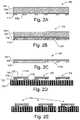
- FIGS. 1A-1Dare simplified cross-sectional views of the process of mounting GaN LEDs 10 to a submount 12 and removing the sapphire growth substrate 24 .
- the submount 12may be formed of silicon or may be a ceramic insulator. If the submount 12 is silicon, an oxide layer may insulate the metal pattern on the submount surface from the silicon, or different schemes of ion implantation can be realized for added functionality such as electrostatic discharge protection.
- a number of LED dies 10are formed with a thin GaN LED layer 18 formed on a sapphire growth substrate 24 .
- Electrodes 16are formed in electrical contact with the n-type and p-type layers in the GaN layer 18 .
- Gold stud bumps 20are placed on the electrodes 16 on the LEDs 10 or alternatively on the metal pads 14 on the submount 12 .
- the gold stud bumps 20are generally spherical gold balls placed at various points between the LED electrodes 16 and the submount metal pads 14 .
- the LED layers 18 and electrodes 16are all formed on the same sapphire substrate 24 , which is then diced to form the individual LED dies 10 .
- the LEDs 10are bonded to the substrate 12 with the metal pads 14 on the submount 12 electrically bonded to the metal electrodes 16 on the GaN layers 18 .
- Pressureis applied to the LED structure while an ultrasonic transducer rapidly vibrates the LED structure with respect to the submount to create heat at the interface. This causes the surface of the gold stud bumps to interdiffuse at the atomic level into the LED electrodes and submount electrodes to create a permanent electrical connection.
- Other types of bonding methodsinclude soldering, applying a conductive paste, and other means.
- underfill 22Between the LED layers 18 and the surface of the submount 12 there is a large void that is filled with an epoxy to provide mechanical support and to seal the area, as illustrated in FIG. 1C .
- the resulting epoxyis referred to as an underfill 22 .
- Underfillingis very time-consuming since each LED dies 10 must be underfilled separately, and a precise amount of underfill material needs to be injected.
- the underfill materialmust be a low enough viscosity that it can flow under the LED dies 10 , which may include a complicated geometry of electrodes, without trapping any bubbles that could result in poorly supported regions, as illustrated as region 22 a .
- the underfill materialhowever, must not spread in an uncontrolled fashion onto undesirable surfaces, such as the top of the LED device, as illustrated at 22 b , or pads on the submount where wire bonds must be subsequently applied.
- the sapphire substrates 24are removed after the LED dies 10 are bonded to the submount 12 and the submount 12 is separated into individual elements to form the LED structures illustrated in FIG. 1D .
- the underfillserves the additional purpose to provide the necessary mechanical support to prevent fracturing of the fragile LED layers when the supporting substrate 24 is removed.
- the gold stud bumps 20do not provide sufficient support by themselves to prevent fracturing of the LED layers since, given their limited shape and are spaced far apart.
- Conventionally used underfill materialsare typically composed of organic substances and possess very different thermal expansion properties from metal and semiconductor materials. Such spurious expansion behavior is particularly aggravated at high operating temperatures—typical of high power LED applications—where underfill materials approach their glass transition point and begin to behave as elastic substances. The net effect of such mismatch in thermal expansion behavior is to induce stresses on the LED devices that limit or reduce their operability at high power conditions.
- underfill materialshave low thermal conductivity properties that result in unnecessarily high temperature operation for the semiconductor devices.
- a light emitting diodeis fabricated using an underfill layer that is deposited on either the LED or the submount prior to mounting the LED to a submount.
- the deposition of the underfill layer prior to mounting the LED to the submountprovides for a more uniform and void free support, and increases underfill material options to permit improved thermal characteristics.
- the underfill layermay be deposited on the LEDs and used support for the thin and brittle LED layers during the removal of the growth substrate. The growth substrate can then be removed at the wafer level prior to mounting the LED to the submount.
- the underfill layermay be patterned and/or polished back so that only the contact areas of the LED and/or submount are exposed. The LEDs and submount can then be bonded with the underfill layer between them.
- the patterned underfill layermay also be used as a guide to assist in the singulating of the devices.
- FIGS. 1A-1Dare simplified cross-sectional views of the process of mounting LEDs to a submount, followed by injecting an underfill and removing the sapphire growth substrate.
- FIGS. 2A-2Eare simplified cross-sectional views of a process of removing the growth substrate from LEDs on the wafer level and mounting the LEDs to a submount in accordance with one embodiment of the present invention.
- FIG. 3illustrates a portion of the LED structure including a sapphire growth substrate and GaN layers.
- FIGS. 4A and 4Billustrate the deposition of the underfill material over a portion of the LEDs at the wafer level.
- FIGS. 5A-5Care simplified cross-sectional views of mounting LEDs to a submount and removing the growth substrate after the LEDs are mounted to the submount.
- FIGS. 6A-6Eare simplified cross-sectional views of a process of mounting LEDs to a submount that has an underfill coating.
- FIGS. 7A-7Dillustrate another embodiment in which wafer level LEDs with a patterned underfill layer are mounted to a submount.
- FIGS. 8A-8Gillustrate another embodiment in which individual LED dies are mounted to a submount on which an underfill layer has been deposited.
- FIGS. 2A-2Eare simplified cross-sectional views of a process of mounting GaN LEDs to a submount and removing the growth substrate in accordance with one embodiment of the present invention.
- FIG. 2Aillustrates a portion of a wafer level LED structure 100 including a growth substrate 102 , which may be, e.g., sapphire, upon which has been formed the thin GaN LED layers 104 .
- the GaN LED layers 104may be conventionally grown on the sapphire substrate, as described, e.g., in U.S. Publication No. 2007/0096130, which is incorporated herein by reference.
- FIG. 3illustrates a portion of the wafer structure 100 including a sapphire substrate 102 over which an n-type GaN layer 104 n is grown using conventional techniques.
- the GaN layer 104 nmay be multiple layers including a clad layer.
- the GaN layer 104 nmay include Al, In, and an n-type dopant.
- An active layer 104 ais then grown over the GaN layer 104 n.
- the active layer 104 nwill typically be multiple GaN-based layers and its composition (e.g., In x Al y Ga 1-x-y N) depends on the desired wavelength of the light emission and other factors.
- the active layer 104 amay be conventional.
- a p-type GaN layer 104 pis then grown over the active layer 104 a.
- the GaN layer 104 pmay be multiple layers including a clad layer and may also be conventional.
- the GaN layer 104 pmay include Al, In, and a p-type dopant.
- the LED structure of FIG. 3is referred to as a double heterostructure.
- the growth substrateis about 90 microns thick, and the GaN layers 104 have a combined thickness of approximately 4 microns.
- GaN based LED with a sapphire growth substrateis used in the example, other types of LEDs using other substrates such as SiC (used to form an InAlGaN LED) and GaAs (used to form an AlInGaP LED) may benefit from the present invention.
- SiCused to form an InAlGaN LED
- GaAsused to form an AlInGaP LED
- contacts 108Metal bonding layers are formed over the wafer to form n-contacts 108 n and p-contacts 108 p , referred to herein as contacts 108 .
- the contacts 108may be patterned by forming a masking layer at positions where the metal contacts are not desired, then depositing the metal contact layer over the entire wafer, and then stripping the masking layer to lift off the metal deposited over it.
- the metal layerscould also be negatively patterned by depositing similarly stacked blanket metal layers and then selectively etching them back using a masking scheme.
- the contactsmay be formed from one or more metals, such as TiAu, Au, Cu, Al, Ni or other ductile material, or a combination of such layers.
- Stud bumps 110which may be, e.g., gold, are then formed over the contacts 108 .
- the stud bumps 110are generally spherical gold balls placed at various points on the contact 108 .
- the stud bumps 110serve as part of the contacts for the LED and are used to bond the LED to a submount. If desired, other types of bonding material or structures such as plates may be used in place of stud bumps 110 .
- the underfill 120is then deposited over the GaN layers 104 , contacts 108 and bumps 110 . Because the underfill 120 is applied prior to bonding the LEDs to a submount, any suitable material may be used for the underfill 120 without depending on the flow characteristics that are needed in the case of traditional underfill.
- a polymer polyimide based materialswhich have high glass transition temperature, may be used as the underfill layer 120 .
- a solventmay be used to adjust the viscosity to 400-1000 Pa*s to assist in the deposition of the material.
- a filler powdersuch as small particle SiO 2
- the LEDs and polyimide materialmay be heated below the glass transition temperature, and then allowed to cool down to cure. Such materials will help the device withstand high temperature/high current condition without deformation of thin LEDs.
- the underfill materialmay be a bi-stage cured material, using a low temperature cure for cross-linking of additives, e.g., epoxy additives, in the underfill material that are responsible for the first stage cure.
- the underfill materialshould have B-stage cure properties in order to adhere to both LED and support wafer surfaces.
- FIGS. 4A and 4Billustrate the deposition of the underfill 120 material over a portion of the wafer 100 .
- the underfill 120may be blanket deposited over the surface of the GaN layers 104 .
- the underfill 120is patterned, e.g., using stencil printing or mesh screen-printing, so that areas 122 , such as area where the LED dies are to be separated, have no underfill 120 .
- the materialmay be deposited in the form of a viscous paste using, e.g., stencil printing techniques. Areas where underfill is not desired, e.g., the areas around the LEDs where there is wire bonding, are protected by a mask.
- Openings in the maskallow the underfill material to be deposited in desired areas.
- the underfill layeris cured at low temperature, e.g., 120°-130° C., until it is sufficiently hard to be polished.
- the underfill 120is then polished back until the metal connection, i.e., bumps 110 , are exposed.
- the underfill 120has a final thickness of 30 ⁇ m.
- the underfill 120advantageously serves as a support layer for the GaN layers 104 and, accordingly, the growth substrate 102 can be removed, as illustrated in FIG. 2C .
- the substrate 102can be removed, e.g., by laser lift-off using an excimer laser beam that is transmitted through the transparent sapphire substrate 102 and evaporates a top layer of the n-GaN layer 104 n.
- the removal of the substrate 102produces tremendous pressure at the substrate/n-GaN layer 104 n interface. The pressure forces the substrate 102 off the n-GaN layer 104 n , and the substrate 102 is removed.
- the support provided by the underfill 120prevents the high pressure during the substrate lift-off from fracturing the thin brittle LED layers 104 .
- the exposed n layer 104 nmay be roughened for increasing light extraction, e.g., using photo-electro-chemical etching, or by small scale imprinting or grinding.
- rougheningcan include forming prisms or other optical elements on the surface for increased light extraction and improved control of the radiation pattern.
- the GaN layers 104 with the underfill 120are scribed and separated into individual LED elements.
- the scribing and separationmay be accomplished using, e.g., a saw that uses the areas 122 in the underfill 120 as a guide. Alternatively, a laser scribe process may be used.
- a sawthat uses the areas 122 in the underfill 120 as a guide.
- a laser scribe processmay be used.
- the wafer of LEDsPrior to separating, the wafer of LEDs is adhered to a stretchable plastic sheet, and after the wafer is broken along the scribe lines, the sheet is stretched to separate the dies while the dies remain adhered to the stretchable sheet.
- An automatic pick and place devicethen removes each die 125 from the sheet, and mounts the die 125 on a submount 130 as illustrated in FIG. 2D .
- the bonding metali.e., bumps 110 on the LED dies 125 are ultrasonically or thermosonically welded directly to corresponding bonding metal patterns 132 on the submount 130 , which may be, e.g., gold or other appropriate material.
- the submount 130may be formed of silicon or a ceramic insulator. If the submount 130 is silicon, an oxide layer may insulate the metal pattern on the submount surface from the silicon, or different schemes of ion implantation can be realized for added functionality such as Zener diodes for electro-discharge protection. If the submount is a ceramic instead of silicon, the metal patterns can be directly formed on the ceramic surfaces.
- An ultrasonic transducermay be used to apply a downward pressure to the dies 125 and rapidly vibrates the dies 125 with respect to the submount 130 so that the atoms from the opposing bonding metals merge to create an electrical and mechanical connection between the die 125 and the submount 130 .
- Other methods for LED die-to-submount interconnectioncan also be used, such as using a soldering layer.
- the substrate temperatureis maintained above (e.g., 40-50° C.) the glass transition temperature Tg, which causes the underfill material to be in the elastic stage to soften and comply with the LEDs and to prevent the formation of voids.
- the underfill layeris permitted to cure at approximately the glass transition temperature, e.g., 200° C., for 1-2 hours in order to harden.
- the submount 130can then be scribed and singulated to form LEDs 140 as illustrated in FIG. 2E .
- the growth substrate 102is not removed until after the wafer is separated into separate dies and mounted to the submount 130 , as illustrated in FIGS. 5A , 5 B, and 5 C.
- the sapphire substrate 102 with LED GaN layers 104are scribed and separated into individual dies 150 .
- the scribing and separationmay be accomplished using, e.g., a saw that cuts through the sapphire substrate 102 using areas 122 in the underfill 120 as a guide.
- the separate dies 150are then mounted to the submount 130 , as described above. Once the dies 150 are mounted to the submount 130 , the sapphire substrate 102 can be lifted-off described above and as illustrated in FIG. 5B .
- the submount 130is then singulated to form LEDs 140 , as illustrated in FIG. 5C .
- FIGS. 6A-6Eare simplified cross-sectional views of a process of mounting GaN LEDs to a submount with an underfill coating.
- FIG. 6Aillustrates a portion of a submount 202 with bonding metal patterns 204 with bumps 206 .
- a silicon submount 202 with Au bonding metal patterns 204 and Au bumps 206may be used.
- other materialsmay be used if desired.
- An underfill layer 210is deposited over submount 202 , bonding metal patterns 204 and bumps 206 .
- the underfill layer 210may be patterned, e.g., using stencil printing or mesh screen-printing, so that areas, such as area where the LED dies are to be separated, have no underfill material.
- any suitable materialmay be used for the underfill 210 without depending on the flow characteristics that are needed in the case of traditional underfill.
- a polymer polyimide based materialswhich have high glass transition temperature, may be used as the underfill layer 210 .
- the underfill materialshould have B-stage cure properties in order to adhere to both LED and support wafer surfaces.
- an inorganic dielectric materialmay be used if desired. As illustrated in FIG. 6B , the underfill layer 210 is polished back until the metal connection, i.e., bumps 206 , are exposed.
- a growth substrate 230 with an LED GaN layer 232 and contacts 234is separated into separate LED dies 235 , which are then mounted on the submount 202 with underfill layer 210 as illustrated in FIG. 6C .
- the contacts on the LED dies 234are ultrasonically or thermosonically welded directly to corresponding the bonding bumps 206 on the submount 130 , as described above.
- the growth substrate 230is removed, e.g., using a laser lift-off process, resulting in the structure illustrated shown in FIG. 6D .
- the submount 202is then singulated to form LEDs 240 , as illustrated in FIG. 6E .
- FIGS. 7A-7Dillustrate wafer level LEDs with a patterned underfill layer that are mounted to a submount in accordance with another embodiment.
- FIG. 7Ais a simplified cross-sectional view of portions of wafer level LEDs 300 with a patterned underfill layer 310 and FIG. 7B is a plan view of the bottom surface of the wafer level LEDs 300 along line AA shown in FIG. 7A .
- the wafer level LEDs 300include a growth substrate 302 along with LED layers 304 and contacts 306 .
- the underfill layer 310is deposited, e.g., using stencil printing or mesh screen-printing to form a pattern that exposes the contacts 306 on the bottom surface of the LED layers 304 and cured.
- the underfill patternmatches the pattern of contacts 322 that are present on the submount 320 , as can be seen in FIG. 7C so that only the areas where the LEDs will be attached are exposed.
- the wafer level LEDs 300are mounted at the wafer level with a submount 320 with contacts 322 .
- the waver level LEDs 300are mounted to the submount 320 , e.g. ultrasonically or thermosonically, to bond the contacts 306 on the LED layers 304 with the contacts 322 on the submount 320 , as described above.
- the growth substrate 302can then be lift-off, e.g., using a laser lift-off process, and the LEDs singulated into individual dies.
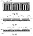
- FIGS. 8A-8Gillustrate another embodiment in which individual LED dies are mounted to a submount on which an underfill layer has been deposited.
- FIG. 8Ais a simplified cross-sectional view of portions of a submount 402 with contacts 404 .
- FIG. 8Bis a plan view of the top surface of the submount 402 along line BB shown in FIG. 8A .
- an underfill layer 410is deposited over the submount 402 and in particular is patterned to cover the contacts 404 . Once the underfill layer 410 cures, the underfill layer 410 is polished back to expose the contacts 404 , as illustrated in FIG. 8D and FIG. 8E , which illustrates another plan view of the submount 402 .
- LED dies 420each of which includes a growth substrate 422 , LED layers 424 and contacts 426 on the bottom surface of the LED layers 424 are then individually mounted to the submount 402 , as illustrated in FIG. 8F .
- the growth substrate 422can be lifted off, as illustrated in FIG. 8G , and the submount 402 can be singulated to form individual LED elements as described above.
Landscapes
- Engineering & Computer Science (AREA)
- Computer Hardware Design (AREA)
- Microelectronics & Electronic Packaging (AREA)
- Power Engineering (AREA)
- Led Device Packages (AREA)
- Led Devices (AREA)
Abstract
Description
Claims (18)
Priority Applications (9)
| Application Number | Priority Date | Filing Date | Title |
|---|---|---|---|
| US11/775,059US7867793B2 (en) | 2007-07-09 | 2007-07-09 | Substrate removal during LED formation |
| KR1020107002836AKR101535168B1 (en) | 2007-07-09 | 2008-07-03 | Substrate removal during led formation |
| PCT/IB2008/052681WO2009007886A1 (en) | 2007-07-09 | 2008-07-03 | Substrate removal during led formation |
| RU2010104249/28ARU2466480C2 (en) | 2007-07-09 | 2008-07-03 | Substrate removal during light-emitting diode formation |
| CN2008800241373ACN101743648B (en) | 2007-07-09 | 2008-07-03 | Substrate removal during LED formation |
| EP08776562.4AEP2168178B1 (en) | 2007-07-09 | 2008-07-03 | Substrate removal during led formation |
| JP2010515636AJP5654344B2 (en) | 2007-07-09 | 2008-07-03 | Removal of substrate in LED formation |
| BRPI0814501ABRPI0814501B1 (en) | 2007-07-09 | 2008-07-03 | method to fabricate a led structure |
| TW97125489ATWI467796B (en) | 2007-07-09 | 2008-07-04 | Substrate removal during formation of light-emitting diodes |
Applications Claiming Priority (1)
| Application Number | Priority Date | Filing Date | Title |
|---|---|---|---|
| US11/775,059US7867793B2 (en) | 2007-07-09 | 2007-07-09 | Substrate removal during LED formation |
Publications (2)
| Publication Number | Publication Date |
|---|---|
| US20090017566A1 US20090017566A1 (en) | 2009-01-15 |
| US7867793B2true US7867793B2 (en) | 2011-01-11 |
Family
ID=39952224
Family Applications (1)
| Application Number | Title | Priority Date | Filing Date |
|---|---|---|---|
| US11/775,059Active2028-06-05US7867793B2 (en) | 2007-07-09 | 2007-07-09 | Substrate removal during LED formation |
Country Status (9)
| Country | Link |
|---|---|
| US (1) | US7867793B2 (en) |
| EP (1) | EP2168178B1 (en) |
| JP (1) | JP5654344B2 (en) |
| KR (1) | KR101535168B1 (en) |
| CN (1) | CN101743648B (en) |
| BR (1) | BRPI0814501B1 (en) |
| RU (1) | RU2466480C2 (en) |
| TW (1) | TWI467796B (en) |
| WO (1) | WO2009007886A1 (en) |
Cited By (5)
| Publication number | Priority date | Publication date | Assignee | Title |
|---|---|---|---|---|
| US8350251B1 (en) | 2011-09-26 | 2013-01-08 | Glo Ab | Nanowire sized opto-electronic structure and method for manufacturing the same |
| US8669125B2 (en) | 2010-06-18 | 2014-03-11 | Glo Ab | Nanowire LED structure and method for manufacturing the same |
| US9640681B2 (en) | 2012-05-23 | 2017-05-02 | Samsung Display Co., Ltd. | Window structure, method of manufacturing the same, electronic device equipped with a camera including a window structure and method of manufacturing the same |
| US9721812B2 (en)* | 2015-11-20 | 2017-08-01 | International Business Machines Corporation | Optical device with precoated underfill |
| US20230402442A1 (en)* | 2022-10-26 | 2023-12-14 | Shanghai Tianma Micro-electronics Co., Ltd. | Method for manufacturing display panel, display panel, and display apparatus |
Families Citing this family (28)
| Publication number | Priority date | Publication date | Assignee | Title |
|---|---|---|---|---|
| JP2008186959A (en)* | 2007-01-29 | 2008-08-14 | Toyoda Gosei Co Ltd | III-V group semiconductor device and manufacturing method thereof |
| JP4290745B2 (en)* | 2007-03-16 | 2009-07-08 | 豊田合成株式会社 | Method for manufacturing group III-V semiconductor device |
| US20090230409A1 (en)* | 2008-03-17 | 2009-09-17 | Philips Lumileds Lighting Company, Llc | Underfill process for flip-chip leds |
| JP4724222B2 (en) | 2008-12-12 | 2011-07-13 | 株式会社東芝 | Method for manufacturing light emitting device |
| KR101601622B1 (en)* | 2009-10-13 | 2016-03-09 | 삼성전자주식회사 | Light emitting diode divice Light emitting appratus and Manufacturing method of light emitting diode divice |
| CN102194985B (en)* | 2010-03-04 | 2013-11-06 | 展晶科技(深圳)有限公司 | Wafer level package method |
| JP5343040B2 (en)* | 2010-06-07 | 2013-11-13 | 株式会社東芝 | Semiconductor light emitting device |
| JP2012094716A (en)* | 2010-10-27 | 2012-05-17 | Asahi Kasei E-Materials Corp | Connection structure and manufacturing method thereof |
| KR101591991B1 (en)* | 2010-12-02 | 2016-02-05 | 삼성전자주식회사 | Light emitting device package and method thereof |
| TW201403892A (en)* | 2012-07-10 | 2014-01-16 | Lextar Electronics Corp | Substrate of light-emitting diode and method of solid crystal using the same |
| JP6089507B2 (en)* | 2012-08-31 | 2017-03-08 | 日亜化学工業株式会社 | Light emitting device and manufacturing method thereof |
| JP2014179569A (en)* | 2013-03-15 | 2014-09-25 | Nichia Chem Ind Ltd | Light-emitting device and method of manufacturing the same |
| US9548247B2 (en) | 2013-07-22 | 2017-01-17 | Infineon Technologies Austria Ag | Methods for producing semiconductor devices |
| CN105489746B (en)* | 2014-09-19 | 2018-02-23 | 展晶科技(深圳)有限公司 | The manufacture method of light emitting chip module, light emitting diode and light emitting chip module |
| JP6519127B2 (en)* | 2014-09-19 | 2019-05-29 | 日亜化学工業株式会社 | Method of manufacturing light emitting device |
| CN106159058A (en)* | 2015-04-09 | 2016-11-23 | 江西省晶瑞光电有限公司 | A kind of LED encapsulation structure and preparation method thereof |
| CN105244423B (en)* | 2015-10-30 | 2018-11-20 | 漳州立达信光电子科技有限公司 | Packaging method of substrateless LED chip and substrateless LED chip |
| US10461068B2 (en)* | 2017-03-15 | 2019-10-29 | The United States Of America As Represented By The Secretary Of The Air Force | Highly integrated RF power and power conversion based on Ga2O3 technology |
| WO2018223391A1 (en)* | 2017-06-09 | 2018-12-13 | Goertek. Inc | Micro-led array transfer method, manufacturing method and display device |
| US10490428B2 (en)* | 2017-12-22 | 2019-11-26 | Lumidleds LLC | Method and system for dual stretching of wafers for isolated segmented chip scale packages |
| US10964867B2 (en) | 2018-10-08 | 2021-03-30 | Facebook Technologies, Llc | Using underfill or flux to promote placing and parallel bonding of light emitting diodes |
| JP7257187B2 (en)* | 2019-03-05 | 2023-04-13 | 東レエンジニアリング株式会社 | Chip transfer plate, chip transfer method, image display device manufacturing method, and semiconductor device manufacturing method |
| US11404600B2 (en) | 2019-06-11 | 2022-08-02 | Meta Platforms Technologies, Llc | Display device and its process for curing post-applied underfill material and bonding packaging contacts via pulsed lasers |
| US11575069B2 (en) | 2019-06-11 | 2023-02-07 | Meta Platforms Technologies, Llc | Employing deformable contacts and pre-applied underfill for bonding LED devices via lasers |
| US11164844B2 (en)* | 2019-09-12 | 2021-11-02 | Taiwan Semiconductor Manufacturing Company, Ltd. | Double etch stop layer to protect semiconductor device layers from wet chemical etch |
| CN116325945A (en)* | 2020-10-08 | 2023-06-23 | 富士通株式会社 | Base station device, terminal station device, wireless communication system, and wireless communication method |
| CN113611786B (en)* | 2021-08-02 | 2022-09-27 | 东莞市中麒光电技术有限公司 | LED chip bulk transfer method with high peeling yield and convenient film pouring |
| TWI812015B (en)* | 2022-02-16 | 2023-08-11 | 友達光電股份有限公司 | Light-emitting diode display and manufacturing method of the same |
Citations (20)
| Publication number | Priority date | Publication date | Assignee | Title |
|---|---|---|---|---|
| US5128746A (en) | 1990-09-27 | 1992-07-07 | Motorola, Inc. | Adhesive and encapsulant material with fluxing properties |
| US6245595B1 (en) | 1999-07-22 | 2001-06-12 | National Semiconductor Corporation | Techniques for wafer level molding of underfill encapsulant |
| WO2001047039A1 (en) | 1999-12-22 | 2001-06-28 | Lumileds Lighting, U.S., Llc | Method of making a iii-nitride light-emitting device with increased light generating capability |
| US6352881B1 (en) | 1999-07-22 | 2002-03-05 | National Semiconductor Corporation | Method and apparatus for forming an underfill adhesive layer |
| US6399426B1 (en) | 1998-07-21 | 2002-06-04 | Miguel Albert Capote | Semiconductor flip-chip package and method for the fabrication thereof |
| JP2002271014A (en) | 2001-03-09 | 2002-09-20 | Hitachi Kokusai Electric Inc | Electronic component mounting method |
| US20030148024A1 (en)* | 2001-10-05 | 2003-08-07 | Kodas Toivo T. | Low viscosity precursor compositons and methods for the depositon of conductive electronic features |
| US6838311B2 (en)* | 2001-10-12 | 2005-01-04 | Advanced Semiconductor Engineering, Inc. | Flip chip package and method for forming the same |
| US20050012208A1 (en) | 2003-07-18 | 2005-01-20 | Samsung Electronics Co., Ltd. | Method of surface-mounting semiconductor chip on PCB |
| US6869832B2 (en) | 2003-02-07 | 2005-03-22 | Lockheed Martin Corporation | Method for planarizing bumped die |
| WO2005062905A2 (en) | 2003-12-24 | 2005-07-14 | Gelcore Llc | Laser lift-off of sapphire from a nitride flip-chip |
| US20050161779A1 (en) | 2004-01-26 | 2005-07-28 | Hui Peng | Flip chip assemblies and lamps of high power GaN LEDs, wafer level flip chip package process, and method of fabricating the same |
| US6943061B1 (en) | 2004-04-12 | 2005-09-13 | Ns Electronics Bangkok (1993) Ltd. | Method of fabricating semiconductor chip package using screen printing of epoxy on wafer |
| US20060043402A1 (en) | 2004-08-31 | 2006-03-02 | Toyoda Gosei Co., Ltd. | Light emitting device and light emitting element |
| EP1653523A2 (en) | 2004-10-28 | 2006-05-03 | LumiLeds Lighting U.S., LLC | Light emitting diode package |
| WO2006131843A2 (en) | 2005-06-09 | 2006-12-14 | Koninklijke Philips Electronics N.V. | Method of removing the growth substrate of a semiconductor light-emitting device |
| WO2007009042A1 (en) | 2005-07-11 | 2007-01-18 | Gelcore Llc | Laser lift-off led with improved light extraction |
| US20070096130A1 (en) | 2005-06-09 | 2007-05-03 | Philips Lumileds Lighting Company, Llc | LED Assembly Having Maximum Metal Support for Laser Lift-Off of Growth Substrate |
| WO2008007235A2 (en) | 2006-06-09 | 2008-01-17 | Koninklijke Philips Electronics N.V. | Semiconductor light emitting device including porous layer |
| WO2008038249A2 (en) | 2006-09-28 | 2008-04-03 | Koninklijke Philips Electronics N.V. | Process for preparing a semiconductor structure for mounting and mounted optoelectronic semiconductor structure |
Family Cites Families (9)
| Publication number | Priority date | Publication date | Assignee | Title |
|---|---|---|---|---|
| US5376580A (en)* | 1993-03-19 | 1994-12-27 | Hewlett-Packard Company | Wafer bonding of light emitting diode layers |
| RU2142176C1 (en)* | 1997-06-10 | 1999-11-27 | Карпович Нина Васильевна | Light source |
| JP3906653B2 (en)* | 2000-07-18 | 2007-04-18 | ソニー株式会社 | Image display device and manufacturing method thereof |
| JP3589187B2 (en)* | 2000-07-31 | 2004-11-17 | 日亜化学工業株式会社 | Method for forming light emitting device |
| WO2002033750A1 (en)* | 2000-10-17 | 2002-04-25 | 3M Innovative Properties Company | Solvent assisted burnishing of pre-underfilled solder-bumped wafers for flipchip bonding |
| RU2200358C1 (en)* | 2001-06-05 | 2003-03-10 | Хан Владимир Александрович | Semiconductor light-emitting diode |
| US7019330B2 (en)* | 2003-08-28 | 2006-03-28 | Lumileds Lighting U.S., Llc | Resonant cavity light emitting device |
| JP4438492B2 (en)* | 2003-09-11 | 2010-03-24 | 日亜化学工業株式会社 | Semiconductor device and manufacturing method thereof |
| US7932111B2 (en)* | 2005-02-23 | 2011-04-26 | Cree, Inc. | Substrate removal process for high light extraction LEDs |
- 2007
- 2007-07-09USUS11/775,059patent/US7867793B2/enactiveActive
- 2008
- 2008-07-03RURU2010104249/28Apatent/RU2466480C2/enactive
- 2008-07-03WOPCT/IB2008/052681patent/WO2009007886A1/enactiveApplication Filing
- 2008-07-03BRBRPI0814501Apatent/BRPI0814501B1/enactiveIP Right Grant
- 2008-07-03KRKR1020107002836Apatent/KR101535168B1/enactiveActive
- 2008-07-03EPEP08776562.4Apatent/EP2168178B1/enactiveActive
- 2008-07-03CNCN2008800241373Apatent/CN101743648B/enactiveActive
- 2008-07-03JPJP2010515636Apatent/JP5654344B2/enactiveActive
- 2008-07-04TWTW97125489Apatent/TWI467796B/enactive
Patent Citations (22)
| Publication number | Priority date | Publication date | Assignee | Title |
|---|---|---|---|---|
| US5128746A (en) | 1990-09-27 | 1992-07-07 | Motorola, Inc. | Adhesive and encapsulant material with fluxing properties |
| US6399426B1 (en) | 1998-07-21 | 2002-06-04 | Miguel Albert Capote | Semiconductor flip-chip package and method for the fabrication thereof |
| US6245595B1 (en) | 1999-07-22 | 2001-06-12 | National Semiconductor Corporation | Techniques for wafer level molding of underfill encapsulant |
| US6352881B1 (en) | 1999-07-22 | 2002-03-05 | National Semiconductor Corporation | Method and apparatus for forming an underfill adhesive layer |
| WO2001047039A1 (en) | 1999-12-22 | 2001-06-28 | Lumileds Lighting, U.S., Llc | Method of making a iii-nitride light-emitting device with increased light generating capability |
| JP2002271014A (en) | 2001-03-09 | 2002-09-20 | Hitachi Kokusai Electric Inc | Electronic component mounting method |
| US20030148024A1 (en)* | 2001-10-05 | 2003-08-07 | Kodas Toivo T. | Low viscosity precursor compositons and methods for the depositon of conductive electronic features |
| US6838311B2 (en)* | 2001-10-12 | 2005-01-04 | Advanced Semiconductor Engineering, Inc. | Flip chip package and method for forming the same |
| US6869832B2 (en) | 2003-02-07 | 2005-03-22 | Lockheed Martin Corporation | Method for planarizing bumped die |
| US20050012208A1 (en) | 2003-07-18 | 2005-01-20 | Samsung Electronics Co., Ltd. | Method of surface-mounting semiconductor chip on PCB |
| WO2005062905A2 (en) | 2003-12-24 | 2005-07-14 | Gelcore Llc | Laser lift-off of sapphire from a nitride flip-chip |
| US20050161779A1 (en) | 2004-01-26 | 2005-07-28 | Hui Peng | Flip chip assemblies and lamps of high power GaN LEDs, wafer level flip chip package process, and method of fabricating the same |
| US6943061B1 (en) | 2004-04-12 | 2005-09-13 | Ns Electronics Bangkok (1993) Ltd. | Method of fabricating semiconductor chip package using screen printing of epoxy on wafer |
| US20060043402A1 (en) | 2004-08-31 | 2006-03-02 | Toyoda Gosei Co., Ltd. | Light emitting device and light emitting element |
| EP1653523A2 (en) | 2004-10-28 | 2006-05-03 | LumiLeds Lighting U.S., LLC | Light emitting diode package |
| EP1653523A3 (en) | 2004-10-28 | 2009-02-11 | Philips Lumileds Lighting Company LLC | Light emitting diode package |
| WO2006131843A2 (en) | 2005-06-09 | 2006-12-14 | Koninklijke Philips Electronics N.V. | Method of removing the growth substrate of a semiconductor light-emitting device |
| US20060281203A1 (en)* | 2005-06-09 | 2006-12-14 | Lumileds Lighting U.S, Llc | Method of removing the growth substrate of a semiconductor light emitting device |
| US20070096130A1 (en) | 2005-06-09 | 2007-05-03 | Philips Lumileds Lighting Company, Llc | LED Assembly Having Maximum Metal Support for Laser Lift-Off of Growth Substrate |
| WO2007009042A1 (en) | 2005-07-11 | 2007-01-18 | Gelcore Llc | Laser lift-off led with improved light extraction |
| WO2008007235A2 (en) | 2006-06-09 | 2008-01-17 | Koninklijke Philips Electronics N.V. | Semiconductor light emitting device including porous layer |
| WO2008038249A2 (en) | 2006-09-28 | 2008-04-03 | Koninklijke Philips Electronics N.V. | Process for preparing a semiconductor structure for mounting and mounted optoelectronic semiconductor structure |
Cited By (11)
| Publication number | Priority date | Publication date | Assignee | Title |
|---|---|---|---|---|
| US8669125B2 (en) | 2010-06-18 | 2014-03-11 | Glo Ab | Nanowire LED structure and method for manufacturing the same |
| US9117990B2 (en) | 2010-06-18 | 2015-08-25 | Glo Ab | Nanowire LED structure and method for manufacturing the same |
| US9312442B2 (en) | 2010-06-18 | 2016-04-12 | Glo Ab | Nanowire structure and method for manufacturing the same |
| US8350251B1 (en) | 2011-09-26 | 2013-01-08 | Glo Ab | Nanowire sized opto-electronic structure and method for manufacturing the same |
| US8937295B2 (en) | 2011-09-26 | 2015-01-20 | Glo Ab | Nanowire sized opto-electronic structure and method for manufacturing the same |
| US9419183B2 (en) | 2011-09-26 | 2016-08-16 | Glo Ab | Nanowire sized opto-electronic structure and method for manufacturing the same |
| US9640681B2 (en) | 2012-05-23 | 2017-05-02 | Samsung Display Co., Ltd. | Window structure, method of manufacturing the same, electronic device equipped with a camera including a window structure and method of manufacturing the same |
| US10134922B2 (en) | 2012-05-23 | 2018-11-20 | Samsung Display Co., Ltd. | Window structure, method of manufacturing the same, electronic device equipped with a camera including a window structure and method of manufacturing the same |
| US9721812B2 (en)* | 2015-11-20 | 2017-08-01 | International Business Machines Corporation | Optical device with precoated underfill |
| US20230402442A1 (en)* | 2022-10-26 | 2023-12-14 | Shanghai Tianma Micro-electronics Co., Ltd. | Method for manufacturing display panel, display panel, and display apparatus |
| US12176334B2 (en)* | 2022-10-26 | 2024-12-24 | Shanghai Tianma Micro-electronics Co., Ltd. | Method for manufacturing display panel, display panel, and display apparatus |
Also Published As
| Publication number | Publication date |
|---|---|
| US20090017566A1 (en) | 2009-01-15 |
| CN101743648A (en) | 2010-06-16 |
| KR101535168B1 (en) | 2015-07-09 |
| KR20100047255A (en) | 2010-05-07 |
| TWI467796B (en) | 2015-01-01 |
| BRPI0814501B1 (en) | 2018-12-11 |
| JP2010533374A (en) | 2010-10-21 |
| EP2168178B1 (en) | 2019-03-20 |
| BRPI0814501A2 (en) | 2015-02-03 |
| CN101743648B (en) | 2013-02-06 |
| RU2466480C2 (en) | 2012-11-10 |
| EP2168178A1 (en) | 2010-03-31 |
| JP5654344B2 (en) | 2015-01-14 |
| WO2009007886A1 (en) | 2009-01-15 |
| RU2010104249A (en) | 2011-08-20 |
| TW200924237A (en) | 2009-06-01 |
Similar Documents
| Publication | Publication Date | Title |
|---|---|---|
| US7867793B2 (en) | Substrate removal during LED formation | |
| US7736945B2 (en) | LED assembly having maximum metal support for laser lift-off of growth substrate | |
| JP6712579B2 (en) | Method of mounting light emitting device on supporting substrate | |
| TWI437724B (en) | Robust light-emitting diode structure for substrate stripping | |
| TWI569469B (en) | P-N separation metal filling for flip chip light-emitting diode | |
| EP2438625B1 (en) | Method of forming a dielectric layer on a semiconductor light emitting device, and semiconductor light emitting device with a dielectric layer | |
| CN105340089A (en) | LED with stress buffer layer under metallization layer | |
| EP2831930B1 (en) | Sealed semiconductor light emitting device and method of forming thereof | |
| US7732231B1 (en) | Method of forming a dielectric layer on a semiconductor light emitting device | |
| TWI672836B (en) | Semiconductor light emitting device and manufacturing method thereof | |
| US9362471B2 (en) | Semiconductor light emitting device with thick metal layers | |
| CN1971952A (en) | Converse welding method of high power LED chip | |
| WO2013084103A1 (en) | Semiconductor light emitting device with thick metal layers |
Legal Events
| Date | Code | Title | Description |
|---|---|---|---|
| AS | Assignment | Owner name:PHILIPS LUMILEDS LIGHTING COMPANY LLC, CALIFORNIA Free format text:ASSIGNMENT OF ASSIGNORS INTEREST;ASSIGNORS:BASIN, GRIGORIY;WEST, ROBERT S.;MARTIN, PAUL S.;REEL/FRAME:019532/0706;SIGNING DATES FROM 20070607 TO 20070709 Owner name:PHILIPS LUMILEDS LIGHTING COMPANY LLC, CALIFORNIA Free format text:ASSIGNMENT OF ASSIGNORS INTEREST;ASSIGNORS:BASIN, GRIGORIY;WEST, ROBERT S.;MARTIN, PAUL S.;SIGNING DATES FROM 20070607 TO 20070709;REEL/FRAME:019532/0706 | |
| STCF | Information on status: patent grant | Free format text:PATENTED CASE | |
| FPAY | Fee payment | Year of fee payment:4 | |
| AS | Assignment | Owner name:DEUTSCHE BANK AG NEW YORK BRANCH, AS COLLATERAL AGENT, NEW YORK Free format text:SECURITY INTEREST;ASSIGNOR:LUMILEDS LLC;REEL/FRAME:043108/0001 Effective date:20170630 Owner name:DEUTSCHE BANK AG NEW YORK BRANCH, AS COLLATERAL AG Free format text:SECURITY INTEREST;ASSIGNOR:LUMILEDS LLC;REEL/FRAME:043108/0001 Effective date:20170630 | |
| MAFP | Maintenance fee payment | Free format text:PAYMENT OF MAINTENANCE FEE, 8TH YEAR, LARGE ENTITY (ORIGINAL EVENT CODE: M1552) Year of fee payment:8 | |
| MAFP | Maintenance fee payment | Free format text:PAYMENT OF MAINTENANCE FEE, 12TH YEAR, LARGE ENTITY (ORIGINAL EVENT CODE: M1553); ENTITY STATUS OF PATENT OWNER: LARGE ENTITY Year of fee payment:12 | |
| AS | Assignment | Owner name:LUMILEDS SINGAPORE PTE. LTD., SINGAPORE Free format text:ASSIGNMENT OF ASSIGNORS INTEREST;ASSIGNOR:LUMILEDS LLC;REEL/FRAME:071888/0086 Effective date:20250708 |