US7862857B2 - Scalable lead zirconium titanate (PZT) thin film material and deposition method, and ferroelectric memory device structures comprising such thin film material - Google Patents
Scalable lead zirconium titanate (PZT) thin film material and deposition method, and ferroelectric memory device structures comprising such thin film materialDownload PDFInfo
- Publication number
- US7862857B2 US7862857B2US12/768,374US76837410AUS7862857B2US 7862857 B2US7862857 B2US 7862857B2US 76837410 AUS76837410 AUS 76837410AUS 7862857 B2US7862857 B2US 7862857B2
- Authority
- US
- United States
- Prior art keywords
- pzt
- thd
- scalable
- ferroelectric
- zirconium
- Prior art date
- Legal status (The legal status is an assumption and is not a legal conclusion. Google has not performed a legal analysis and makes no representation as to the accuracy of the status listed.)
- Expired - Fee Related
Links
Images


Classifications
- H—ELECTRICITY
- H01—ELECTRIC ELEMENTS
- H01L—SEMICONDUCTOR DEVICES NOT COVERED BY CLASS H10
- H01L21/00—Processes or apparatus adapted for the manufacture or treatment of semiconductor or solid state devices or of parts thereof
- H01L21/02—Manufacture or treatment of semiconductor devices or of parts thereof
- H01L21/02104—Forming layers
- H01L21/02107—Forming insulating materials on a substrate
- H01L21/02109—Forming insulating materials on a substrate characterised by the type of layer, e.g. type of material, porous/non-porous, pre-cursors, mixtures or laminates
- H01L21/02112—Forming insulating materials on a substrate characterised by the type of layer, e.g. type of material, porous/non-porous, pre-cursors, mixtures or laminates characterised by the material of the layer
- H01L21/02172—Forming insulating materials on a substrate characterised by the type of layer, e.g. type of material, porous/non-porous, pre-cursors, mixtures or laminates characterised by the material of the layer the material containing at least one metal element, e.g. metal oxides, metal nitrides, metal oxynitrides or metal carbides
- H01L21/02197—Forming insulating materials on a substrate characterised by the type of layer, e.g. type of material, porous/non-porous, pre-cursors, mixtures or laminates characterised by the material of the layer the material containing at least one metal element, e.g. metal oxides, metal nitrides, metal oxynitrides or metal carbides the material having a perovskite structure, e.g. BaTiO3
- H—ELECTRICITY
- H10—SEMICONDUCTOR DEVICES; ELECTRIC SOLID-STATE DEVICES NOT OTHERWISE PROVIDED FOR
- H10D—INORGANIC ELECTRIC SEMICONDUCTOR DEVICES
- H10D84/00—Integrated devices formed in or on semiconductor substrates that comprise only semiconducting layers, e.g. on Si wafers or on GaAs-on-Si wafers
- H10D84/80—Integrated devices formed in or on semiconductor substrates that comprise only semiconducting layers, e.g. on Si wafers or on GaAs-on-Si wafers characterised by the integration of at least one component covered by groups H10D12/00 or H10D30/00, e.g. integration of IGFETs
- C—CHEMISTRY; METALLURGY
- C04—CEMENTS; CONCRETE; ARTIFICIAL STONE; CERAMICS; REFRACTORIES
- C04B—LIME, MAGNESIA; SLAG; CEMENTS; COMPOSITIONS THEREOF, e.g. MORTARS, CONCRETE OR LIKE BUILDING MATERIALS; ARTIFICIAL STONE; CERAMICS; REFRACTORIES; TREATMENT OF NATURAL STONE
- C04B35/00—Shaped ceramic products characterised by their composition; Ceramics compositions; Processing powders of inorganic compounds preparatory to the manufacturing of ceramic products
- C04B35/01—Shaped ceramic products characterised by their composition; Ceramics compositions; Processing powders of inorganic compounds preparatory to the manufacturing of ceramic products based on oxide ceramics
- C04B35/48—Shaped ceramic products characterised by their composition; Ceramics compositions; Processing powders of inorganic compounds preparatory to the manufacturing of ceramic products based on oxide ceramics based on zirconium or hafnium oxides, zirconates, zircon or hafnates
- C04B35/49—Shaped ceramic products characterised by their composition; Ceramics compositions; Processing powders of inorganic compounds preparatory to the manufacturing of ceramic products based on oxide ceramics based on zirconium or hafnium oxides, zirconates, zircon or hafnates containing also titanium oxides or titanates
- C04B35/491—Shaped ceramic products characterised by their composition; Ceramics compositions; Processing powders of inorganic compounds preparatory to the manufacturing of ceramic products based on oxide ceramics based on zirconium or hafnium oxides, zirconates, zircon or hafnates containing also titanium oxides or titanates based on lead zirconates and lead titanates, e.g. PZT
- C—CHEMISTRY; METALLURGY
- C07—ORGANIC CHEMISTRY
- C07C—ACYCLIC OR CARBOCYCLIC COMPOUNDS
- C07C49/00—Ketones; Ketenes; Dimeric ketenes; Ketonic chelates
- C07C49/92—Ketonic chelates
- C—CHEMISTRY; METALLURGY
- C07—ORGANIC CHEMISTRY
- C07F—ACYCLIC, CARBOCYCLIC OR HETEROCYCLIC COMPOUNDS CONTAINING ELEMENTS OTHER THAN CARBON, HYDROGEN, HALOGEN, OXYGEN, NITROGEN, SULFUR, SELENIUM OR TELLURIUM
- C07F7/00—Compounds containing elements of Groups 4 or 14 of the Periodic Table
- C07F7/003—Compounds containing elements of Groups 4 or 14 of the Periodic Table without C-Metal linkages
- C—CHEMISTRY; METALLURGY
- C23—COATING METALLIC MATERIAL; COATING MATERIAL WITH METALLIC MATERIAL; CHEMICAL SURFACE TREATMENT; DIFFUSION TREATMENT OF METALLIC MATERIAL; COATING BY VACUUM EVAPORATION, BY SPUTTERING, BY ION IMPLANTATION OR BY CHEMICAL VAPOUR DEPOSITION, IN GENERAL; INHIBITING CORROSION OF METALLIC MATERIAL OR INCRUSTATION IN GENERAL
- C23C—COATING METALLIC MATERIAL; COATING MATERIAL WITH METALLIC MATERIAL; SURFACE TREATMENT OF METALLIC MATERIAL BY DIFFUSION INTO THE SURFACE, BY CHEMICAL CONVERSION OR SUBSTITUTION; COATING BY VACUUM EVAPORATION, BY SPUTTERING, BY ION IMPLANTATION OR BY CHEMICAL VAPOUR DEPOSITION, IN GENERAL
- C23C16/00—Chemical coating by decomposition of gaseous compounds, without leaving reaction products of surface material in the coating, i.e. chemical vapour deposition [CVD] processes
- C23C16/22—Chemical coating by decomposition of gaseous compounds, without leaving reaction products of surface material in the coating, i.e. chemical vapour deposition [CVD] processes characterised by the deposition of inorganic material, other than metallic material
- C23C16/30—Deposition of compounds, mixtures or solid solutions, e.g. borides, carbides, nitrides
- C23C16/40—Oxides
- C23C16/409—Oxides of the type ABO3 with A representing alkali, alkaline earth metal or lead and B representing a refractory metal, nickel, scandium or a lanthanide
- H—ELECTRICITY
- H01—ELECTRIC ELEMENTS
- H01G—CAPACITORS; CAPACITORS, RECTIFIERS, DETECTORS, SWITCHING DEVICES, LIGHT-SENSITIVE OR TEMPERATURE-SENSITIVE DEVICES OF THE ELECTROLYTIC TYPE
- H01G4/00—Fixed capacitors; Processes of their manufacture
- H01G4/002—Details
- H01G4/018—Dielectrics
- H01G4/06—Solid dielectrics
- H01G4/08—Inorganic dielectrics
- H01G4/12—Ceramic dielectrics
- H01G4/1209—Ceramic dielectrics characterised by the ceramic dielectric material
- H01G4/1236—Ceramic dielectrics characterised by the ceramic dielectric material based on zirconium oxides or zirconates
- H01G4/1245—Ceramic dielectrics characterised by the ceramic dielectric material based on zirconium oxides or zirconates containing also titanates
- H—ELECTRICITY
- H10—SEMICONDUCTOR DEVICES; ELECTRIC SOLID-STATE DEVICES NOT OTHERWISE PROVIDED FOR
- H10B—ELECTRONIC MEMORY DEVICES
- H10B53/00—Ferroelectric RAM [FeRAM] devices comprising ferroelectric memory capacitors
- H—ELECTRICITY
- H10—SEMICONDUCTOR DEVICES; ELECTRIC SOLID-STATE DEVICES NOT OTHERWISE PROVIDED FOR
- H10B—ELECTRONIC MEMORY DEVICES
- H10B53/00—Ferroelectric RAM [FeRAM] devices comprising ferroelectric memory capacitors
- H10B53/30—Ferroelectric RAM [FeRAM] devices comprising ferroelectric memory capacitors characterised by the memory core region
- H—ELECTRICITY
- H10—SEMICONDUCTOR DEVICES; ELECTRIC SOLID-STATE DEVICES NOT OTHERWISE PROVIDED FOR
- H10D—INORGANIC ELECTRIC SEMICONDUCTOR DEVICES
- H10D1/00—Resistors, capacitors or inductors
- H10D1/60—Capacitors
- H10D1/68—Capacitors having no potential barriers
- H10D1/682—Capacitors having no potential barriers having dielectrics comprising perovskite structures
- C—CHEMISTRY; METALLURGY
- C04—CEMENTS; CONCRETE; ARTIFICIAL STONE; CERAMICS; REFRACTORIES
- C04B—LIME, MAGNESIA; SLAG; CEMENTS; COMPOSITIONS THEREOF, e.g. MORTARS, CONCRETE OR LIKE BUILDING MATERIALS; ARTIFICIAL STONE; CERAMICS; REFRACTORIES; TREATMENT OF NATURAL STONE
- C04B2235/00—Aspects relating to ceramic starting mixtures or sintered ceramic products
- C04B2235/02—Composition of constituents of the starting material or of secondary phases of the final product
- C04B2235/30—Constituents and secondary phases not being of a fibrous nature
- C04B2235/44—Metal salt constituents or additives chosen for the nature of the anions, e.g. hydrides or acetylacetonate
- C04B2235/441—Alkoxides, e.g. methoxide, tert-butoxide
- C—CHEMISTRY; METALLURGY
- C04—CEMENTS; CONCRETE; ARTIFICIAL STONE; CERAMICS; REFRACTORIES
- C04B—LIME, MAGNESIA; SLAG; CEMENTS; COMPOSITIONS THEREOF, e.g. MORTARS, CONCRETE OR LIKE BUILDING MATERIALS; ARTIFICIAL STONE; CERAMICS; REFRACTORIES; TREATMENT OF NATURAL STONE
- C04B2235/00—Aspects relating to ceramic starting mixtures or sintered ceramic products
- C04B2235/02—Composition of constituents of the starting material or of secondary phases of the final product
- C04B2235/30—Constituents and secondary phases not being of a fibrous nature
- C04B2235/44—Metal salt constituents or additives chosen for the nature of the anions, e.g. hydrides or acetylacetonate
- C04B2235/449—Organic acids, e.g. EDTA, citrate, acetate, oxalate
- C—CHEMISTRY; METALLURGY
- C04—CEMENTS; CONCRETE; ARTIFICIAL STONE; CERAMICS; REFRACTORIES
- C04B—LIME, MAGNESIA; SLAG; CEMENTS; COMPOSITIONS THEREOF, e.g. MORTARS, CONCRETE OR LIKE BUILDING MATERIALS; ARTIFICIAL STONE; CERAMICS; REFRACTORIES; TREATMENT OF NATURAL STONE
- C04B2235/00—Aspects relating to ceramic starting mixtures or sintered ceramic products
- C04B2235/70—Aspects relating to sintered or melt-casted ceramic products
- C04B2235/96—Properties of ceramic products, e.g. mechanical properties such as strength, toughness, wear resistance
- C04B2235/963—Surface properties, e.g. surface roughness
- H—ELECTRICITY
- H01—ELECTRIC ELEMENTS
- H01G—CAPACITORS; CAPACITORS, RECTIFIERS, DETECTORS, SWITCHING DEVICES, LIGHT-SENSITIVE OR TEMPERATURE-SENSITIVE DEVICES OF THE ELECTROLYTIC TYPE
- H01G4/00—Fixed capacitors; Processes of their manufacture
- H01G4/33—Thin- or thick-film capacitors (thin- or thick-film circuits; capacitors without a potential-jump or surface barrier specially adapted for integrated circuits, details thereof, multistep manufacturing processes therefor)
- H—ELECTRICITY
- H01—ELECTRIC ELEMENTS
- H01L—SEMICONDUCTOR DEVICES NOT COVERED BY CLASS H10
- H01L21/00—Processes or apparatus adapted for the manufacture or treatment of semiconductor or solid state devices or of parts thereof
- H01L21/02—Manufacture or treatment of semiconductor devices or of parts thereof
- H01L21/02104—Forming layers
- H01L21/02107—Forming insulating materials on a substrate
- H01L21/02109—Forming insulating materials on a substrate characterised by the type of layer, e.g. type of material, porous/non-porous, pre-cursors, mixtures or laminates
- H01L21/02205—Forming insulating materials on a substrate characterised by the type of layer, e.g. type of material, porous/non-porous, pre-cursors, mixtures or laminates the layer being characterised by the precursor material for deposition
- H—ELECTRICITY
- H01—ELECTRIC ELEMENTS
- H01L—SEMICONDUCTOR DEVICES NOT COVERED BY CLASS H10
- H01L21/00—Processes or apparatus adapted for the manufacture or treatment of semiconductor or solid state devices or of parts thereof
- H01L21/02—Manufacture or treatment of semiconductor devices or of parts thereof
- H01L21/02104—Forming layers
- H01L21/02107—Forming insulating materials on a substrate
- H01L21/02225—Forming insulating materials on a substrate characterised by the process for the formation of the insulating layer
- H01L21/0226—Forming insulating materials on a substrate characterised by the process for the formation of the insulating layer formation by a deposition process
- H01L21/02263—Forming insulating materials on a substrate characterised by the process for the formation of the insulating layer formation by a deposition process deposition from the gas or vapour phase
- H01L21/02271—Forming insulating materials on a substrate characterised by the process for the formation of the insulating layer formation by a deposition process deposition from the gas or vapour phase deposition by decomposition or reaction of gaseous or vapour phase compounds, i.e. chemical vapour deposition
Definitions
- This inventionrelates generally to a novel lead zirconium titanate (PZT) material having unique properties and application for PZT thin film capacitors, as well as to a deposition method for forming PZT films of such material, and ferroelectric capacitor structures employing such thin film material.
- PZTlead zirconium titanate
- DRAMsdynamic random access memories
- FeRAMsferroelectric random access memories
- ferroelectric SrBi 2 Ta 2 O 9SBT
- Pb(Zr,Ti)O 3PZT
- SBTferroelectric SrBi 2 Ta 2 O 9
- PZTPb(Zr,Ti)O 3
- Pt/SBT/Pt capacitorsfor example, have been shown to have excellent fatigue and retention characteristics, although processing temperatures in excess of 750° C. pose integration issues.
- phase-pure thin filmscan be deposited at temperatures in the 450-650° C. range, although Pt/PZT/Pt capacitors are known to suffer from poor fatigue and retention.
- doping and/or oxide electrodeshave been needed to produce satisfactory capacitor electrical properties.
- E ccoercive field
- film thicknessa combination of adequately low coercive field (E c ) and film thickness.
- SBT filmshave been shown to have low E c ( ⁇ 35 kV/cm) at thicknesses on the order of 140 nm, resulting in coercive voltages of 0.5V.
- SBTis handicapped by a low value of switched ferroelectric polarization (P sw ), typically less than 25 ⁇ C/cm 2 .
- P swswitched ferroelectric polarization
- thermal processing800° C.
- the high ferroelectric polarization and low processing temperatures of PZTprovide a compelling motivation to identify a form of PZT and a deposition process that allows scaling the material to low operating voltages.
- a still further object of the inventionis to provide a PZT material that is useful for ferroelectric capacitors over a broad range of pulse lengths, particularly in the range of from about 5 nanoseconds to about 200 microseconds.
- the present inventionrelates generally to a novel lead zirconium titanate (PZT) material, as well as to a deposition method for forming PZT thin films of such material, and ferroelectric capacitor structures employing such thin film material.
- PZTlead zirconium titanate
- E cis the electric field at which the polarization is zero during a polarization versus voltage hysteresis loop.
- the E-field frequencyis 50 Hertz for this purpose.
- Leakage current densityJ is measured at the operating voltage, V op , and a step voltage response at 5 seconds.
- Retentionis the remanent polarization as measured by the method described in Integrated Ferroelectrics, Vol. 16 [669], No. 3, page 63 (1997).
- “Cycling fatigue P sw ,”is the ferroelectric polarization measured with a frequency of 0.5 MegaHertz or slower square pulse, at a 50% duty cycle, and a capacitor area of ⁇ 10 ⁇ 4 cm 2 .
- “Dimensionally-scalable PZT” materialmeans a PZT material that is un-doped and has useful ferroelectric properties for PZT thin film capacitors over a range of thickness of from about 20 to about 150 nanometers, and with lateral dimensions as low as 0.15 ⁇ m and lower, and corresponding capacitor areas from about 10 4 to about 10 ⁇ 2 ⁇ m 2 .
- E-field scalable PZTmaterial means a PZT material that is un-doped and has useful ferroelectric properties for PZT thin film capacitors over the range of film thickness of 20 to 150 nanometers, at a voltage below 3 Volts.
- PZT materialmeans a PZT material that is un-doped and has useful ferroelectric properties over a range of excitation (voltage) pulse length from 5 nanoseconds to 200 microseconds.
- “Ferroelectric operating voltage”means a voltage that when applied to a PZT thin film in a capacitor causes the material to be dielectrically switched from one to another of its orientational polar states.
- Platinum effect determinationmeans establishing a correlative empirical matrix of plots of each of ferroelectric polarization, leakage current density and atomic percent lead in PZT films, as a function of each of temperature, pressure and liquid precursor solution A/B ratio, wherein A/B ratio is the ratio of Pb to (Zr+Ti), and identifying from the plots the “knee” or inflection point of each plot as defining a region of operation with respect to the independent process variables of temperature, pressure and liquid precursor solution A/B ratio, and conducting the MOCVD process at a corresponding value of the temperature, pressure and liquid precursor solution A/B ratio selected from such region of operation, as hereinafter described.
- Type 1 propertiesmeans, collectively, a ferroelectric polarization P sw greater than 20 microCoulombs ( ⁇ C) per square centimeter, a leakage current density (J) less than 10 ⁇ 5 amperes per square centimeter at operating voltage, a dielectric relaxation defined by J ⁇ n log (time) wherein n is greater than 0.5 and a cycling fatigue defined by P sw being less than 10% lower than its original value after 10 10 polarization switching cycles.
- Type 2 propertiesmeans, collectively, the following dimensionally scaled properties of ferroelectric polarization, coercive E-field, leakage current density, retention and cycling fatigue:
- Un-doped in reference to PZT film materialmeans that the dopants and modifiers (heterologous atomic species that are added into the crystal structure of the PZT material and are responsible for the observed or enhanced ferroelectric properties of the material) are present in the material at concentrations of less than 1 atomic percent.
- the present inventionrelates to a dimensionally scalable, pulse length scalable and/or E-field scalable ferroelectric PZT material.
- Another aspect of the inventionrelates to a ferroelectric PZT material having Type 1 and/or Type 2 characteristics.
- the inventionrelates to a ferroelectric PZT material that has at least one, more preferably at least two, still more preferably at least three, and most preferably all four, of the Type 1 properties.
- the present inventionrelates to a ferroelectric PZT material having at least one of the Type 2 properties and progressively more preferably having two, three, four or five of such properties.
- the inventionrelates in another aspect to a ferroelectric PZT material capacitor comprising a ferroelectric PZT material of a dimensionally-scalable, pulse length scalable and/or E-field scalable character, and a capacitor area of from about 10 4 to about 10 ⁇ 2 ⁇ m 2 .
- a FeRAM deviceincluding a capacitor comprising a ferroelectric PZT material of a dimensionally-scalable, pulse length scalable and/or E-field scalable character, and a capacitor area of from about 10 4 to about 10 ⁇ 2 ⁇ m 2 .
- the inventionin another aspect, relates to a method of fabricating a ferroelectric PZT film on a substrate, comprising forming the film by liquid delivery MOCVD on the substrate under MOCVD conditions producing a ferroelectric film on the substrate having Type 1 and/or Type 2 characteristics.
- a further aspect of the inventionrelates to a method of fabricating a ferroelectric PZT film on a substrate, comprising forming the film by liquid delivery MOCVD on the substrate under MOCVD conditions including nucleation conditions producing a dimensionally scalable, pulse length scalable and/or E-field scalable PZT film on the substrate.
- Another aspect of the inventionrelates to a method of fabricating a ferroelectric PZT film on a substrate, comprising forming the film by liquid delivery MOCVD on the substrate under MOCVD conditions including temperature, pressure and liquid precursor solution A/B ratio determined by plateau effect determination from a correlative empirical matrix of plots of each of ferroelectric polarization, leakage current density and atomic percent lead in PZT films, as a function of each of temperature, pressure and liquid precursor solution A/B ratio, wherein A/B ratio is the ratio of Pb to (Zr+Ti).
- a further aspect of the inventionrelates to a method of fabricating a ferroelectric PZT film on a substrate, comprising forming the film by liquid delivery MOCVD on the substrate under MOCVD conditions including Correlative Materials or Processing Requirements, to yield a ferroelectric PZT film having PZT Properties, wherein such Correlative Materials or Processing Requirements and PZT Properties comprise:
- a still further method aspect of the present inventionrelates to a method of fabricating a FeRAM device, comprising forming a capacitor on a substrate including a ferroelectric PZT material of a dimensionally-scalable, pulse length-scalable and/or E-field scalable character, wherein the PZT material is deposited by liquid delivery MOCVD under processing conditions yielding a ferroelectric film on the substrate having Type 1 and/or Type 2 characteristics as such ferroelectric PZT material.
- Yet another aspect of the inventionrelates to a mixture of liquid precursor solutions comprising precursors of lead, zirconium and titanium dissolved or suspended in a solvent medium, wherein the precursors of lead, zirconium and titanium do not undergo ligand exchange.
- a further aspect of the inventionrelates to a precursor vapor composition
- a precursor vapor compositioncomprising precursors of lead, zirconium and titanium, wherein the precursors of lead, zirconium and titanium do not undergo ligand exchange.
- FIG. 1is a graph of film composition (A/B) f as a function of gas-phase composition (A/B) g for a PZT thin film material, showing the insensitivity of the stoichiometry to the precursor concentration.
- FIG. 2is a model data matrix derived for empirically determined values of the logarithm of the leakage current density (Log J), the ferroelectric polarization (P sw ) and atomic % Pb in the film, as a function of pressure (P), temperature (T) and solution A/B ratio.
- FIG. 3is a schematic cross-section of a semiconductor device utilizing a stack capacitor configuration.
- FIG. 4is a plot of TGA data comparing Pb and Ti compounds with Zr(thd) 4 and Zr(O-i-Pr) 2 (thd) 2 .
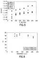
- FIG. 5is a plot of current density versus E-field for PZT films varying thickness showing the current density is only weakly dependent on film thickness above ⁇ 125 nm.
- FIG. 6is a plot of coercive field (E u ) versus film thickness showing that E c is nearly independent of film thickness.
- FIG. 7is a plot of a) P sw versus voltage; and b) P sw versus electric field.
- FIG. 8is a plot of P*-P ⁇ versus number of cycles for PZT films showing that fatigue is nearly independent of film thickness.
- FIG. 9is a plot of imprint behavior for PZT films of varying thickness.
- FIG. 10shows the test configuration for the shunt method of ferroelectric pulse testing.
- FIG. 11is a plot of test signal and response signal versus time for a 10 ⁇ m ⁇ 10 ⁇ m capacitor tested with a 1 ⁇ s pulse.
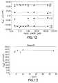
- FIG. 12is a plot of Q sw versus pulse length for various applied voltages showing Q sw to be independent of pulse length over the range investigated.
- FIG. 13is a plot of Q sw versus capacitor dimension showing Q sw to be independent of area over the range investigated.
- the present inventionprovides a unique PZT material that is scalable in character and provides major advantages over the prior art in application to the formation and use of PZT in ferroelectric thin film capacitor structures.
- the PZT material of the present inventionis useful for ferroelectric capacitors over a wide range of thicknesses, e.g., from about 20 nanometers to about 150 nanometers, and a range of lateral dimensions extending to as low as 0.15 ⁇ m.
- Corresponding capacitor areas (i.e., lateral scaling) in a preferred embodimentare in the range of from about 10 4 to about 10 ⁇ 2 ⁇ m 2 .
- the foregoing propertiesprovide a dimensional scaling capability that is achievable without PZT film modification techniques such as acceptor doping or the use of film modifiers such as Nb, Ta, La, Sr, Ca and the like.
- the novel PZT material of the present inventionin one embodiment has Type 1 properties, viz., a ferroelectric polarization P s , greater than 20 ⁇ C/cm 2 , a leakage current density J less than 10 ⁇ 5 A/cm 2 at V op , a dielectric relaxation defined by J′ log(time) wherein n is greater than 0.5, and a cycling fatigue defined by P sw being less than 10% lower than its original value after 10 10 polarization switching cycles.
- Type 1 propertiesviz., a ferroelectric polarization P s , greater than 20 ⁇ C/cm 2 , a leakage current density J less than 10 ⁇ 5 A/cm 2 at V op , a dielectric relaxation defined by J′ log(time) wherein n is greater than 0.5, and a cycling fatigue defined by P sw being less than 10% lower than its original value after 10 10 polarization switching cycles.
- Such PZT materialis a substantial advance over the PZT materials of the prior art lacking such Type 1 properties, and the present invention provides a reproducible method of fabricating such material by liquid delivery metalorganic chemical vapor deposition.
- the present inventionrelates in one aspect to a method to deposit thin film ferroelectric materials by MOCVD utilizing a liquid delivery technique.
- This techniqueaffords precise compositional control by virtue of mixing liquid precursor solutions and flash vaporizing them. Flash vaporization has the added benefit of preventing unwanted premature decomposition of the precursor species.
- tailored precursor chemistriesmay be employed that are compatible for forming the thin film material because the precursors do not undergo ligand exchange (or they have degenerate exchange) which prevents the formation of involatile species.
- a process thereforeis desired for the formation of thin films of PZT and related materials, which affords compositional control, provides uniformity of the thin film material over large areas, and achieves a high degree of conformality on the substrate structure as well as a high deposition rate.
- the deposited materialshould also be free of pinholes, since in capacitive structures and in many other devices, pinholes will result in an electrically shorted, useless device.
- the metalorganic precursors of the component metals of the desired PbZr x Ti 1-x O 3 filmare introduced in liquid form, either as neat liquids or dilute solutions if the precursor is a liquid at ambient temperature and pressure (e.g., 25° C. and atmospheric pressure) conditions, or if the precursor composition is a solid at such ambient conditions, then as a solution of the precursor in a compatible solvent medium.
- the solvent mediummay be of any suitable type that is compatible with the specific precursor composition employed, as is known and understood by those skilled in the art of liquid delivery MOCVD, and may be constituted by single-component solvent species, or alternatively by multicomponent solvent mixtures.
- the metalorganic precursors utilized for such liquid delivery techniquemay for example comprise lead bis(2,2,6,6-tetramethyl-3,5-heptanedionate), [Pb(thd) 2 ], as a Pb precursor; titanium bis(isopropoxide)bis(2,2,6,6-tetramethyl-3,5-heptanedionate), [Ti(O-i-Pr) 2 (thd) 2 ], as a Ti precursor; and zirconium tetrakis(2,2,6,6-tetramethyl-3,5-heptanedionate), [Zr(thd) 4 ], as a Zr precursor.
- the lead precursormay comprise lead bis(2,2,6,6-tetramethyl-3,5-heptanedionate) N,N′,N′′-pentamethyl diethylenetriamine, [Pb(thd) 2 pmdeta]
- the zirconium precursormay alternatively comprise zirconium bis(isopropoxide)bis(2,2,6,6-tetramethyl-3,5-heptanedionate), [Zr(O-i-Pr) 2 (thd) 2 ].
- the solvent media used in the liquid delivery MOCVD process of the inventionmay suitably comprise by way of example the solvent compositions that are disclosed in U.S. patent application Ser. No. 08/414,504 filed Mar. 31, 1995 in the names of Robin A. Gardiner, et al., and issued on Dec. 8, 1998 as U.S. Pat. No. 5,820,664, U.S. patent application Ser. No. 08/484,654 filed Jun. 7, 1995 in the names of Robin A. Gardiner, et al., and issued on Aug. 29, 2000 as U.S. Pat. No. 6,110,529, and U.S. patent application Ser. No. 08/975,372 filed Nov. 20, 1997 in the names of Thomas H. Baum, et al., and issued on Jun.
- the solvent mediais comprised of a solution containing approximately 8 parts tetrahydrofuran (THF), 2 parts isopropanol and one part tetraglyme (parts by volume).
- THFtetrahydrofuran
- Pb(thd) 2one or both of the isopropanol and tetraglyme would be excluded from the preferred solvent media.
- Other illustrative multicomponent solvent compositionsinclude a solvent medium comprising octane: decane:polyamine in an 5:4:1 ratio, and a solvent medium comprising octane:polyamine in an 9:1 ratio.
- One particularly preferred single component solvent mediumis tetrahydrofuran (THF).
- the liquid precursor composition once formulatedis introduced into a vaporization zone, in which the liquid is rapidly vaporized, e.g., by flash vaporization on a foraminous vaporization element (e.g., a porous frit element, or a wire, grid or other high surface area structural element) heated to suitable temperature, to produce a corresponding precursor vapor.
- a foraminous vaporization elemente.g., a porous frit element, or a wire, grid or other high surface area structural element
- the precursor vaporthen is transported to the chemical vapor deposition chamber, which may for example comprise a CVD reactor of known or conventional type.
- the CVD systemmay be suitably equipped to introduce the precursor vapor into the deposition chamber for contact with a heated substrate, at a temperature that is suitable to effect deposition of the metal constituents of the vapor onto the substrate element.
- the substratemay be mounted on a heated susceptor or other substrate mounting structure, with the spent vapor from the process being discharged from the deposition chamber and subjected to further treatment or processing in a known and conventional manner.
- the film as depositedmay be further processed in any suitable manner, e.g., by annealing according to a specific time/temperature relationship, and/or in a specific atmosphere or environment, to produce the final desired thin film PbZrTiO 3 material.
- the precursors for the metal components of the product filmare dissolved in a solvent and flash vaporized at temperatures between about 100 to about 300° C. and transported into the MOCVD reactor with a carrier gas (e.g., Ar, N 2 , H 2 , He, or NH 3 ).
- a carrier gase.g., Ar, N 2 , H 2 , He, or NH 3
- the resulting carrier gas/precursor vapor mixturethen may be mixed with an oxidizing co-reactant gas (e.g., O 2 , N 2 O, O 3 or mixtures thereof) and transported to the deposition chamber to undergo decomposition at a substrate heated to a temperature of from about 400° C. to about 1200° C. at chamber pressures in the range of from about 0.1 to about 760 torr.
- Other active oxidizing speciesmay be used to reduce deposition temperature, as through the use of a remote plasma source.
- MOCVD processes for deposition of PZThave the desirable property of the stoichiometry being largely insensitive to process conditions over a fairly wide range of process conditions.
- properties of deposited films with the same stoichiometric compositionare not functionally equivalent.
- the present inventionresolves this incongruity by an approach that identifies process conditions with optimum electrical properties.
- the inventionrelates to a methodology for selection of CVD process conditions that result in PZT films with superior properties.
- the methodologyexploits the “A/B plateau effect” to achieve the fabrication of capacitive PZT films whose electrical properties are congruent with optimum requirements of ferroelectric non-volatile (NV) memories such as ferroelectric random access memories (FeRAMs).
- NVferroelectric non-volatile
- FeRAMsferroelectric random access memories
- Process Set Autilizes a specific precursor chemistry including precursor reagents and solvent compositions, substrate and barrier layer materials (the barrier layer being deposited or otherwise provided between the substrate and the PZT material layer), to provide an electrical environment suitable for the achievement of optimum electrical and performance properties of the PZT material, electrode materials of construction, carrier gas species and oxidant species.
- Process Set AProcess Condition/Material Precursor Chemistry Reagents: [Pb(thd) 2 , Ti(O-i-Pr) 2 (thd) 2 ; Zr(thd) 4 ]
- Solventstetrahydrofuran, glyme solvents, alcohols, hydrocarbon and aryl solvents, amines, polyamines, and mixtures of two or more of the foregoing; examples of illustrative multicomponent solvent compositions are tetrahydrofuran: isopropanol: tetraglyme in a 8:2:1 volume ratio and/or octane:decane:polyamine in a volume ratio of 5:4:1.
- Electrodes and Barriers Bottom ElectrodeIr bottom electrode on TiAIN barrier layer on substrate deposition via sputtering using a collimator and deposition-etch processing
- Top ElectrodeStructures containing Ir and IrO x for top electrode Carrier Gas, Oxidant: Ar, He, H 2 or other inert or non-adverse carrier gas; O 2 , O 3 , N 2 O, O 2 /N 2 O, etc.
- Vaporizeroperate the vaporizer of the liquid delivery system to achieve the foregoing process conditions, as appropriate to the specific vaporizer apparatus employed; examples of vaporizer operating parameters that may be involved include: back pressure, delivery tube ID, frit porosity, vaporizer temperature, gas co-injection, delivery tube/frit composition, and tube/frit installation procedure
- Process Set A elementsare by way of exemplification only, and that the specific precursor chemistries, carrier gas species, device structure layers, etc. may be widely varied in the broad practice of the present invention to achieve a scalable PZT film material within the scope of the present invention.
- the thickness of the ferroelectric film material in the practice of the present inventionmay be widely varied.
- a preferred thickness for FeRAM applicationsis typically in the range of from about 20 to about 150 nanometers.
- Operating voltages for such PZT material films in FeRAM applicationsare typically below 3.3 Volts, down to much lower voltage levels.
- perovskite oxidesThe general formula for perovskite oxides is ABO 3 , where specific metal elements occupy the A and B sites in the crystal lattice, and O is oxygen.
- PZTPb is on the A site and Zr and Ti share the B site. Because the vapor pressure of PbO is lower when its incorporated in the perovskite structure, fairly wide ranges of CVD process parameters result in PZT films with the same or very slightly varying A/B site ratio ⁇ 1.00.
- this A/B “self-correcting effect”is utilized to advantage in the present invention to achieve the formation of PZT material with the properties of: a ferroelectric polarization P sw greater than 20 ⁇ C/cm 2 , a leakage current density J less than 10 ⁇ 5 A/cm 2 at V op , a dielectric relaxation defined by J ⁇ n log(time) wherein n is greater than 0.5, and a cycling fatigue defined by P s , being less than 10% lower than its original value after 10 10 polarization switching cycles (Type 1 properties).
- FIG. 2is a model data matrix derived for empirically determined values of the logarithm of the leakage current density (Log J), the ferroelectric polarization (P sw ) and atomic % Pb in the film, as a function of pressure (P), temperature (T) and solution A/B ratio.
- Model data from the matrixshow the basic relationships between the independent (process variables) P, T and (A/B) solution , on the dependent variables: atomic % Pb in the film, ferroelectric polarization (P sw ) and leakage current density (log J).
- (A/B) solutionis equivalent to (A/B) gas since the precursor liquid reagent solution is vaporized to achieve a same gas-phase composition as is present in the liquid solution of the precursor.
- this “knee” pointis 1.02 for the solution A/B ratio, 1750 millitorr for the deposition pressure, and 575° C. for the deposition temperature.
- the corresponding dependent values producing the superior PZT material of the invention produced with such A/B solution ratio, pressure and temperaturemay be readily determined, including a Log J avg center value of ⁇ 4.35 amperes per square centimeter at operating voltage, Log J avg edge value of ⁇ 6.77 amperes per square centimeter at operating voltage, a P sw edge value of 35.1 ⁇ C per square centimeter, a P sw center value of 33.7 ⁇ C per square centimeter, and an atomic % Pb of 52.3%.
- the present inventionthus encompasses a “plateau effect determination” comprising the steps of establishing a correlative empirical matrix of plots of each of ferroelectric polarization, leakage current density and atomic percent lead in PZT films, as a function of each of temperature, pressure and liquid precursor solution A/B ratio, wherein A/B ratio is the ratio of Pb to (Zr+Ti), and identifying from the plots the “knee” or inflection point of each plot as defining a region of operation with respect to the independent process variables of temperature, pressure and liquid precursor solution A/B ratio, and conducting the MOCVD process at a corresponding value of the temperature, pressure and liquid precursor solution A/B ratio selected from such region of operation, as hereinafter described.
- Table Bis a tabulation listing of the most preferred material properties (Type 2 properties) of the thickness-scalable and dimensionally-scalable PZT material of the invention, wherein t is the film thickness of the PZT material, and 1 is the effective lateral dimension, defined as side of a square with an area that is the same as the capacitor area.
- the inventioncontemplates the use of the “plateau effect” to achieve ferroelectric properties with the scaling properties specified in Table B, as well as the use of nucleation/smoothness methods to achieve ferroelectric properties with the scaling properties that are specified in Table B.
- the ferroelectric PZT material of the inventionthus is a dimensionally scalable material, and suitably comprises at least one of the Table A and/or Table B properties.
- the ferroelectric PZT material of the inventionis also E-field scalable and pulse length scalable in character.
- the PZT material of the present inventionmay be used to form capacitive structures such as FeRAM devices, as well as other microelectronic devices and precursor structures in which PZT may be used to advantage.
- the inventionthus contemplates the provision of a microelectronic device structure including the PZT material of the invention, e.g., a pulse length scalable PZT material of the invention in combination with a power supply and associated power circuitry including such PZT material, as a microelectronic structure arranged for excitation of the PZT material, wherein the excitation is characterized by an excitation (voltage) pulse length in the range of from 5 nanoseconds to 200 nanoseconds.
- the PZT materialmay be used to fabricate a ferroelectric capacitor device structure, by forming a ferroelectric stack capacitor comprising a PZT ferroelectric material of the present invention as a capacitor element on a substrate containing buried transistor circuitry beneath an insulator layer having a via therein containing a conductive plug to the transistor circuitry.
- Such fabrication processmay comprise the steps of patterning, deposition, etch, diffusion, ion implantation, ion bombardment, chemical modification, etc.
- Device 200includes a semiconductor substrate 202 that may include active device structures, not shown, and an insulator layer 204 .
- the semiconductor substrate 202may be silicon, doped silicon, or another semiconductor material.
- the insulator layer 204is deposited on the substrate 202 by any suitable deposition process.
- the insulator layer 204may be, for example, silicon dioxide, silicon nitride, or some combination thereof.
- a conductive diffusion barrier layer 210such as titanium aluminum nitride TiAlN is deposited over the insulator layer 204 .
- a layer of conductive material 212such as iridium, iridium oxide, platinum or combinations thereof, is deposited over the conductive diffusion barrier layer 210 .
- a layer of high dielectric constant material 214such as PZT is deposited by MOCVD over the conductive layer 212 .
- a second layer of conductive material 216such as iridium, iridium oxide, platinum, or combinations thereof, is shown deposited over the layer of high dielectric constant material 214 .
- a diffusion barrier materialsuch as titanium aluminum nitride (TiAlN) will substantially reduce the possibility of diffusion of oxygen during subsequent processing steps that require high temperatures in excess of 500° C.
- Other materialscan be used for the diffusion barrier, such as those disclosed in U.S. patent application Ser. No. 08/994,089 filed Dec. 19, 1997 in the names of Peter S. Kirlin, et al., the disclosure of which hereby is incorporated herein by reference in its entirety.
- FIG. 3shows the portion of the device 200 after the device has been patterned with photoresist and etched. Desired portions of the conductive diffusion barrier layer, upper and lower layers of iridium or other conductive material and of the high dielectric constant material are left to form the upper electrode 216 , capacitor dielectric 214 , lower electrode 212 , and lower electrode barrier layer 210 .
- a layer of interlevel dielectric 218such as silicon dioxide or silicon nitride, is deposited over all.
- the layer of interlevel dielectricis patterned with photoresist and etch to form contact plug holes 221 , 222 , and 223 .
- the insulatoris etched down at the contract plug hole locations 221 and 222 until the iridium or other conductor of the lower electrode 212 and the upper electrode 216 , respectively, are reached.
- the contact plug hole 223is etched down through the insulator layers 218 and 204 until the semiconductor substrate is reached. Once the contact plug openings are prepared, the device 200 is ready for deposition of a layer of oxidation-barrier material.
- FIG. 3shows the semiconductor device 200 following an overall etch of the diffusion barrier layer leaving a diffusion barrier layer 232 in contact with the lower capacitor electrode 212 , a diffusion barrier layer 234 in contact with the upper capacitor electrode 216 , and a diffusion barrier layer 236 in contact with the semiconductor substrate 202 .
- a transfer transistor of the memory cellmay be located below the diffusion barrier layer 236 , but it is not shown.
- the barrier layers 232 , 234 , and 236could be deposited as a single continuous layer prior to the capacitor stack etch and deposition of insulating layer 218 .
- the barrier layercould be patterned and used as a hardmask for the subsequent patterning of the capacitor stack. The alternate process flow would continue with the deposition and patterning of the insulating layer 218 .
- a conductive material, or metallization,is deposited over the interlevel dielectric 218 and the diffusion barrier layers 232 , 234 , and 236 .
- the conductive material 238makes contact with the diffusion barrier layers 232 , 234 , and 236 .
- the conductive material 238may be selected from a group of conductive materials such as aluminum, aluminum alloys, tungsten, tungsten alloys, iridium, and iridium alloys.
- the diffusion barrier layers 232 , 234 , and 236significantly reduce the possibility of any diffusion of the layer of conductive material 238 to the capacitor electrodes 212 and 216 of the semiconductor substrate 202 .
- FIG. 3shown the semiconductor device 200 after the layer of conductive material 238 is patterned and etched to form desired lead lines in the layer of conductive material.
- the patternis formed of photoresist material. Etching is accomplished in accordance with well-established practices known to those of ordinary skill in the semiconductor manufacturing arts.
- a layer of passivation dielectric 240is deposited over the conductive material layer 238 and the interlevel dielectric 218 .
- the passivation dielectricmay be a material such as silicon dioxide, silicon nitride, or other insulator that can provide mechanical and electrical protection for the top surface of the semiconductor device.
- Material of the passivation dielectric layer 240is deposited by well-known techniques.
- the inventioncontemplates as an aspect thereof a microelectronic device structure comprising a PZT material of the present invention. While the invention has been describe herein with reference to specific features, aspects and embodiments, it will be appreciated that the utility of the invention is not thus limited, and that the invention contemplates variations, modifications and embodiments other than those shown and described herein.
- the aforementioned capacitor geometrymay comprise a recessed capacitor geometry, for example, or other structures and conformations that will be readily apparent to those with ordinary skill in the art. Accordingly, the invention is to be broadly interpreted and construed to encompass all such variations and modifications
- the lead precursor chosenwas lead bis(2,2,6,6-tetramethyl-3,5-heptanedionate) [Pb(thd) 2 ].
- Pb(thd) 2lead bis(2,2,6,6-tetramethyl-3,5-heptanedionate)
- This compoundhas no appreciable vapor pressure at room temperature, which makes it much safer to handle than tetra-alkyl lead reagents.
- the low volatility of Pb(thd) 2(0.05 Torr at 180° C.) requires the use of liquid precursor delivery.
- Titanium bis(isopropoxide)bis(2,2,6,6-tetramethyl-3,5-heptanedionate) [Ti(O-i-Pr) 2 (thd) 2 ]was used as the titanium precursor.
- Zr(thd) 4Zirconium tetrakis(2,2,6,6-tetramethyl-3,5-heptanedionate) [Zr(thd) 4 ] was used as the Zr source reagent. These compounds are extremely soluble in organic media and no possible detrimental ligand exchange occurs since the titanium atom is coordinatively saturated.
- the filmwas deposited at 565° C. on Ir/SiO 2 /Si.
- the pressurewas 1.2 Torr
- the oxidizer flowwas a mixture of 500 sccm O 2 and 500 sccm N 2 O
- the reagent flow ratewas 0.14 ml/min for 32.5 minutes.
- XRF analysisgave the following thickness and composition data for the resulting PbZrTiO 3 film:
- the presence of the plateau at (A/B) f values exceeding 1.00may be influenced by inaccuracy in the XRF measurement or by excess Pb diffused into the bottom electrode.
- Analysis of incorporation efficiencies for the metallic constituentsrevealed a decrease in Pb efficiency for (A/B) g >0.83, while Zr and Ti efficiencies remained nearly constant over the same range. This is consistent with the appearance of the plateau, and the absence of PbO from XRD analysis of the films.
- Film thicknessdecreased slightly with increased (A/B) g . This corresponded to an approximate growth rate decrease from 3.8 to 3.2 nm/min.
- the as-deposited filmswere all smooth, dense, and fine-grained.
- the roughness and grain size values calculated from these imagesare given in Table 2 below.
- the measured film roughnesswas insensitive to gas phase composition and was approximately double the starting surface roughness of the Ir films used as substrates.
- PZT films on Ir/MgOdisplayed dominant (001) and (101) PZT orientations; furthermore, the (001)/(101) ratio of PZT peak intensities increased with increased (A/B) g , i.e., oriented toward the tetragonal c-axis with a c-axis lattice constant of 0.406 nm.
- No appreciable (111) PZT texturewas observed on Ir/MgO.
- X-ray diffraction of the as-received substratesrevealed principally (111) oriented Ir; however, a considerable (200) Ir peak was present.
- a central-composite-design experimentwas used to probe a large volume of process space and assess interactions between principal process variables.
- Deposition temperature550, 575, 600° C.
- pressures500, 1750, 3000 mTorr
- A/B g0.53, 0.73, 0.93, 1.13, 1.53
- a constant deposition time of 1660 secondswas used.
- FIG. 4shows comparative TGA data for Pb(thd) 2 , Ti(O-i-Pr) 2 (thd) 2 and two selected Zr compounds: Zr(thd) 4 and Zr(O-i-Pr) 2 (thd) 2 .
- Zr(O-i-Pr) 2 (thd) 2 compoundpossesses an undesirable residuals content of nearly 20% at 400° C., it possesses a desirable thermal stability match with the Pb and Ti compounds commonly used for MOCVD PZT.
- MOCVD PZT depositionswere conducted on standard Ir/TiAlN bottom electrodes (BEs) using the novel Zr(O-i-Pr) 2 (thd) 2 (Zr-2-2) compound with a vaporizer temperature set to 200° C. Additional depositions were processed using the standard Zr(thd) 4 (Zr-0-4) compound at a vaporizer temperature of 203° C. All other deposition conditions were held constant. Following PZT deposition, Pt top electrodes (TEs) were e-beam evaporated, and the samples were annealed at 650° C. in flowing argon for 30 min.
- TEsPt top electrodes
- composition and electrical data for the Zr-2-2 samplesare presented along with data collected from the Zr-0-2 samples.
- the Zr-2-2 samplesthough appreciably lower in Pb and Zr content than the Zr-0-4 samples, were electrically comparable.
- MOCVD PZTmay be prepared using still other novel Zr source precursors.
- Zr 2 (O-i-Pr) 6 (thd) 2has good ambient stability, high volatility and excellent thermal compatibility with Pb and Ti precursors.
- a number of samplesare made up using PZT material formed in accordance with the present invention.
- the samplesare comprised of bottom electrodes formed by sputtering techniques, deposition on the electrodes of PZT material in accordance with the present invention, followed by deposition of top electrodes through a shadow mask by e-beam deposition.
- the PZT deposition timewas varied between 165 sec and 4065 sec to target film a thickness between 10 nm and 260 nm.
- Leakage current density versus E-fieldis given in FIG. 5 .
- the high “leakage” for the 77 nm filmwas directly confirmed.
- the qualitatively different electrical behavior for films below a thickness thresholdmay be due to the high relative roughness (roughness/thickness), which results in some extremely thin regions in thinner films.
- Locally high E-fieldsare expected in those cases.
- Current density for the thicker films in the set (>77 nm)showed remarkably consistent E-field dependence. Leakage in both polarities was in the 10 ⁇ 6 to 10 ⁇ 7 A/cm 2 range for 150 kV/cm. (150 kV/cm corresponds to 1.9 V for the 125 nm film, for example.)
- Leakagewas one of four properties that was insensitive to thickness when plotted as a function of E-field; the other properties were coercive voltage (V c ), polarization saturation (P sw versus V op ), and fatigue endurance.
- E cwas approximately 50 kV/cm.
- FIG. 7shows the dependence of switched polarization on voltage and E-field. The data shows the expected increase of polarization for higher voltages. Clear saturation behavior is seen for the thicker films, which can withstand higher fields. For 125 nm and thicker films, saturated Psw>40 ⁇ C/cm 2 . Normalized to P sw near saturation (300 kV/cm), P sw versus E is nearly independent of film thickness. For all of the samples P sw reaches nearly 90% of it maximum value at 3E c ( ⁇ 150 kV/cm).
- Fatigue properties for this sample setalso displayed consistent properties in terms of E-field scaling ( FIG. 8 ). Fatigue measurements were made at 150 kV/cm, which corresponds to 3E c . The fatigue waveform was a square wave with a period of 10 ⁇ 5 seconds. Fatigue is nearly independent of PZT thickness with a reduction in P sw by ⁇ 50% at 10 9 cycles.
- Static imprintis manifested as an asymmetry in coercive voltage, and is defined as [V c ( ⁇ )+V c (+)]/2.
- FIG. 9show a semi-log plot of imprint voltage versus time.
- the sample used for these measurementsoriginated with a 6-inch diameter Si wafer with an Ir bottom electrode, standard PZT, and a top electrode that consisted of 40 nm of IrO 2 and 60 nm of Ir, as described in Process Set A.
- Individual capacitorswere defined using patterned photoresist and reactive ion etching in a Cl 2 /Ar/O 2 mixture. Following patterning the sample was annealed at 650° C. in flowing oxygen for 30 min.
- the test systemconsisted of an SRS DS345 arbitrary waveform generator, a Tektronix 620B digital storage oscilloscope, and a shunt resistor as shown in FIG. 10 . Details of this testing protocol are further described in P. K. Larsen, G. Kampschoer, M. Ulenaers, G. Spierings and R. Cuppens, Applied Physics Letters, Vol. 59, Issue 5, pp. 611-613 (1991).
- a standard square-pulse ferroelectric pulse trainwas used. This pulse train consisted of one negative polarity pulse, followed by two positive pulses and two negative pulses (set, positive, up, negative, down).
- a typical drive signal, as measured at position X in FIG. 10 , and response signal as measured at position Y in FIG. 10are shown in FIG. 11 .
- Ferroelectric switchingoccurs when a ferroelectric capacitor that has been previously poled by a negative (positive) pulse is poled up (down) by a subsequent positive (negative) pulse.
Landscapes
- Chemical & Material Sciences (AREA)
- Engineering & Computer Science (AREA)
- Organic Chemistry (AREA)
- Ceramic Engineering (AREA)
- Power Engineering (AREA)
- Manufacturing & Machinery (AREA)
- Materials Engineering (AREA)
- Microelectronics & Electronic Packaging (AREA)
- Inorganic Chemistry (AREA)
- Computer Hardware Design (AREA)
- Condensed Matter Physics & Semiconductors (AREA)
- Chemical Kinetics & Catalysis (AREA)
- General Physics & Mathematics (AREA)
- Physics & Mathematics (AREA)
- Structural Engineering (AREA)
- Mechanical Engineering (AREA)
- Metallurgy (AREA)
- General Chemical & Material Sciences (AREA)
- Composite Materials (AREA)
- Semiconductor Memories (AREA)
- Inorganic Insulating Materials (AREA)
- Chemical Vapour Deposition (AREA)
- Fixed Capacitors And Capacitor Manufacturing Machines (AREA)
- Ceramic Capacitors (AREA)
- Internal Circuitry In Semiconductor Integrated Circuit Devices (AREA)
- Formation Of Insulating Films (AREA)
Abstract
Description
| Basic property | Thickness Scaling (t) | Lateral dimension scaling (l) |
| Ferroelectric | Psw> 40 μC/cm2for t > 90 nm | Psw> 30 for l > 1 μm |
| polarization (Psw) | Psw> 30 μC/cm2for t > 50 nm | Psw> 20 for l > 0.05 μm |
| Psw> 20 μC/cm2for t > 20 nm | ||
| Coercive E-field (Ec) | Ec< 100 kV/cm for t > 50 nm | Ec< 100 kV/cm for l > 0.05 μm |
| Ec< 150 kV/cm for t > 20 nm | ||
| Leakage current | J < 10−5A/cm2for t > 90 nm | J < 10−4A/cm2for 1 > 0.05 μm |
| density (J) | J < 10−4A/cm2for t > 50 nm | |
| Retention | <3%/natural log decade (t in | <3%/natural log decade (t in hours) |
| hours) at 150° C., per procedure | at 150° C., per procedure | |
| for t > 50 nm | for l > 0.05 μm | |
| Cycling fatigue Psw | <10% decrease after 1010cycles | <10% decrease after 1010cycles |
| for t > 50 nm | for l > 0.05 μm | |
| <10% decrease after 108cycles | ||
| for t > 20 nm | ||
| Correlative Materials or Processing | |
| PZT Properties | Requirements |
| Basic properties: | |
| Ferroelectric polarization | Film Pb concentration > threshold level; |
| Psw> 20 μC/cm2 | operation on A/B plateau above the knee region, |
| and with temperature, pressure and gas phase | |
| A/B concentration ratio defined by plateau effect | |
| determination | |
| Leakage current density | Film Pb concentration within a range (between |
| J < 10−5A/cm2at operating voltage | the minimum and maximum) on the A/B plateau, |
| and with temperature, pressure and gas phase | |
| A/B concentration ratio defined by plateau effect | |
| determination | |
| Dielectric relaxation | Zr/Ti ratio <45/55 |
| For characteristic J−n∝ log (time), n > 0.5 | Deposition P > 1.8 torr |
| and J < 1% ferroelectric switching current | |
| from 0-100 ns. | |
| Retention | Operation within ranges of temperature, pressure |
| Maintenance of ferroelectric properties | and gas phase A/B concentration ratio defined by |
| (ferroelectric domains) | plateau effect determination |
| Avoidance of cycling fatigue | Use of Ir-based electrodes |
| Psw< 10% decrease after 1010cycles | |
| E-field scalability | Operation within ranges of temperature, pressure |
| and gas phase A/B concentration ratio defined by | |
| plateau effect determination | |
| Surface smoothness | Nucleation-growth conditions during film |
| formation within ranges of temperature, pressure | |
| and gas phase A/B concentration ratio defined by | |
| plateau effect determination | |
| Grain size | Nucleation-growth conditions during film |
| formation within ranges of temperature, pressure | |
| and gas phase A/B concentration ratio defined by | |
| plateau effect determination | |
| TABLE A | |
| Correlative Materials or Processing | |
| PZT property | Requirement(s) |
| Basic properties: | |
| Ferroelectric polarization | Film Pb concentration > threshold level; |
| Psw> 20 μC/cm2 | operation on A/B plateau above the knee region; |
| the A/B plateau determines 3 process parameters: | |
| P, T and gas phase A/B concentration ratio | |
| Leakage current density | Film Pb concentration within a range (between |
| J < 10−5A/cm2at operating voltage | the minimum and maximum) on the A/B plateau; |
| A/B plateau determines 3 process parameters: P, | |
| T and gas phase A/B concentration ratio | |
| Dielectric relaxation | Zr/Ti ratio <45/55 |
| For characteristic J−n∝ log (time), n > 0.5 | Deposition P > 1.8 torr |
| and J < 1% ferroelectric switching current | |
| from 0-100 ns. | |
| Retention | Operation within ranges of P, T and gas phase |
| Maintenance of ferroelectric properties | A/B concentration ratio determined above |
| (ferroelectric domains) | |
| Avoidance of cycling fatigue | Use of Ir-based electrodes |
| Psw< 10% decrease after 1010cycles | |
| E-field scaling | Operation within ranges of P, T and gas phase |
| Achieving qualitative capacitor performance for | A/B concentration ratio determined above |
| films with reduced thickness, and at reduced | |
| voltages | |
| Surface smoothness | Nucleation-growth conditions during film |
| formation within ranges of P, T and gas phase | |
| A/B concentration ratio determined above | |
| Grain size | Nucleation-growth conditions during film |
| formation within ranges of P, T and gas phase | |
| A/B concentration ratio determined above | |
| Process Set A: |
| Process Condition/Material |
| Precursor Chemistry |
| Reagents: [Pb(thd)2, Ti(O-i-Pr)2(thd)2; Zr(thd)4] |
| Solvents: tetrahydrofuran, glyme solvents, alcohols, hydrocarbon and aryl solvents, amines, |
| polyamines, and mixtures of two or more of the foregoing; examples of illustrative multicomponent |
| solvent compositions are tetrahydrofuran: isopropanol: tetraglyme in a 8:2:1 volume ratio and/or |
| octane:decane:polyamine in a volume ratio of 5:4:1. |
| Electrodes and Barriers |
| Bottom Electrode: Ir bottom electrode on TiAIN barrier layer on substrate |
| deposition via sputtering using a collimator and deposition-etch processing |
| Top Electrode: Structures containing Ir and IrOxfor top electrode |
| Carrier Gas, Oxidant: Ar, He, H2or other inert or non-adverse carrier gas; O2, O3, |
| N2O, O2/N2O, etc. as oxidant medium |
| Deposition Conditions: Temperature, Pressure, Precursor Ratio: operate to exploit the plateau |
| effect, in combination with appropriate gas delivery, oxidizer constituents, ratios, flow rates, liquid |
| delivery, liquid flow rate, mixing and deposition time |
| Vaporizer: operate the vaporizer of the liquid delivery system to achieve the foregoing process |
| conditions, as appropriate to the specific vaporizer apparatus employed; examples of vaporizer |
| operating parameters that may be involved include: back pressure, delivery tube ID, frit porosity, |
| vaporizer temperature, gas co-injection, delivery tube/frit composition, and tube/frit installation |
| procedure |
| TABLE B | ||
| Basic property | Thickness Scaling (t) | Lateral dimension scaling (l) |
| Ferroelectric | Psw> 40 μC/cm2for t > 90 nm | Psw> 30 for l > 1 μm |
| polarization (Psw) | Psw> 30 μC/cm2for t > 50 nm | Psw> 20 for l > 0.05 μm |
| Psw> 20 μC/cm2for t > 20 nm | ||
| Coercive E-field (Ec) | Ec< 100 kV/cm for t > 50 nm | Ec< 100 kV/cm for l > 0.05 μm |
| Ec< 150 kV/cm for t > 20 nm | ||
| Leakage current | J < 10−5A/cm2for t > 90 nm | J < 10−4A/cm2for l > 0.05 μm |
| density (J) | J < 10−4A/cm2for t > 50 nm | |
| Retention | <3%/natural log decade (time in | <3%/natural log decade (time in |
| hours) at 150° C., for t > 50 nm | hours) at 150° C., for l > 0.05 μm | |
| Cycling fatigue Psw | <10% decrease after 1010cycles | <10% decrease after 1010cycles |
| for t > 50 nm | for l > 0.05 μm | |
| <10% decrease after 108cycles | ||
| for t > 20 nm | ||
| Operating Parameter | Process Condition | ||
| Substrate temperature | 550~610° | C. |
| Bottom electrode | Ir/SiO2/Si |
| 1~10 | Torr | |||
| Reactor wall temperature | ~210° | C. | ||
| Carrier Ar flow | ~200 | sccm | ||
| O2flow | 500 | sccm | ||
| N2O flow | 500 | sccm | ||
| Total reagent solution concentration | 0.29 | M | ||
| Reagent solution flow rate | 0.1~0.2 | ml/min | ||
| Thickness (μm) | Pb (at. %) | Zr (at. %) | Ti (at. %) | ||
| 0.13 | 52.0 | 23.0 | 25.0 | ||
| TABLE 1 |
| CVD deposition conditions |
| Precursors | Pb(thd)2, Zr(thd)4, Ti(O-i-Pr)2(thd)2 |
| Solution molarity | 0.29 | M | |
| Liquid flow rate | 0.14 | ml/min | |
| Substrate temperature | 550° | C. | |
| Pressure | 1.2 | torr | |
| Deposition rate | 3.5 | nm/min |
| Substrate | Ir/MgO/SiO2/Si | ||
| TABLE 2 |
| Summary of AFM data for PZT/Ir/MgO layers. |
| (A/B)g | (A/B)f | RMS roughness (nm) | Grain size (nm) | ||
| 0.631 | 0.59 | 6.6 | 67 | ||
| 0.731 | 0.97 | 8.4 | 72 | ||
| 0.831 | 1.01 | 7.8 | 86 | ||
| 1.031 | 1.08 | 7.7 | 91 | ||
| Film thickness is nominally 100 nm. | |||||
| TABLE 3 |
| Composition and electrical data for MOCVD PZT films |
| deposited using Zr(O-i-Pr)2(thd)2and Zr(thd)4 |
| Zr(O-i-Pr)2(thd)2 | Zr(thd)4 | ||
| % Pb (at. %) | 49.5 ± 0.07 | 51.8 ± 0.12 |
| Zr: (Zr ± Ti) | 0.322 ± 0.001 | 0.443 ± 0.008 |
| efficiency Pb | 5.99 ± 0.049 | 7.43 ± 0.15 |
| efficiency Zr | 6.54 ± 0.078 | 4.36 ± 0.16 |
| efficiency Ti | 9.31 ± 0.035 | 10.7 ± 0.13 |
| t (nm) | 125 | 128 |
| Psw(μC/cm2) (2 V) | 36 | 38 |
| ±J (A/cm2) (2 V) | 7.4 × 10⁻⁶; −1.5 × 10⁻⁶ | <3 × 10⁻⁶for both |
| polarities | ||
Charge: Q=(1/Rs)

Qsw=(S0+S1)−(P0+P1)
where S0and S1are the leading and trailing edge response pulses for the first switching pulse and P0and P1are the leading and trailing edge pulses for the first non-switching pulse (
Claims (20)
Priority Applications (3)
| Application Number | Priority Date | Filing Date | Title |
|---|---|---|---|
| US12/768,374US7862857B2 (en) | 1999-02-19 | 2010-04-27 | Scalable lead zirconium titanate (PZT) thin film material and deposition method, and ferroelectric memory device structures comprising such thin film material |
| US12/978,393US8501976B2 (en) | 1999-02-19 | 2010-12-23 | Scalable lead zirconium titanate (PZT) thin film material and deposition method, and ferroelectric memory device structures comprising such thin film material |
| US13/960,412US20130324390A1 (en) | 1999-02-19 | 2013-08-06 | Scalable lead zirconium titanate (pzt) thin film material and deposition method, and ferroelectric memory device structures comprising such thin film material |
Applications Claiming Priority (5)
| Application Number | Priority Date | Filing Date | Title |
|---|---|---|---|
| US09/251,890US6316797B1 (en) | 1999-02-19 | 1999-02-19 | Scalable lead zirconium titanate(PZT) thin film material and deposition method, and ferroelectric memory device structures comprising such thin film material |
| US09/928,860US6984417B2 (en) | 1999-02-19 | 2001-08-13 | Scalable lead zirconium titanate (PZT) thin film material and deposition method, and ferroelectric memory device structures comprising such thin film material |
| US11/328,582US7344589B2 (en) | 1999-02-19 | 2006-01-10 | Scalable lead zirconium titanate (PZT) thin film material and deposition method, and ferroelectric memory device structures comprising such thin film material |
| US11/924,716US7705382B2 (en) | 1999-02-19 | 2007-10-26 | Scalable lead zirconium titanate (PZT) thin film material and deposition method, and ferroelectric memory device structures comprising such thin film material |
| US12/768,374US7862857B2 (en) | 1999-02-19 | 2010-04-27 | Scalable lead zirconium titanate (PZT) thin film material and deposition method, and ferroelectric memory device structures comprising such thin film material |
Related Parent Applications (1)
| Application Number | Title | Priority Date | Filing Date |
|---|---|---|---|
| US11/924,716ContinuationUS7705382B2 (en) | 1999-02-19 | 2007-10-26 | Scalable lead zirconium titanate (PZT) thin film material and deposition method, and ferroelectric memory device structures comprising such thin film material |
Related Child Applications (1)
| Application Number | Title | Priority Date | Filing Date |
|---|---|---|---|
| US12/978,393ContinuationUS8501976B2 (en) | 1999-02-19 | 2010-12-23 | Scalable lead zirconium titanate (PZT) thin film material and deposition method, and ferroelectric memory device structures comprising such thin film material |
Publications (2)
| Publication Number | Publication Date |
|---|---|
| US20100209596A1 US20100209596A1 (en) | 2010-08-19 |
| US7862857B2true US7862857B2 (en) | 2011-01-04 |
Family
ID=22953832
Family Applications (7)
| Application Number | Title | Priority Date | Filing Date |
|---|---|---|---|
| US09/251,890Expired - LifetimeUS6316797B1 (en) | 1999-02-19 | 1999-02-19 | Scalable lead zirconium titanate(PZT) thin film material and deposition method, and ferroelectric memory device structures comprising such thin film material |
| US09/928,860Expired - LifetimeUS6984417B2 (en) | 1999-02-19 | 2001-08-13 | Scalable lead zirconium titanate (PZT) thin film material and deposition method, and ferroelectric memory device structures comprising such thin film material |
| US11/328,582Expired - Fee RelatedUS7344589B2 (en) | 1999-02-19 | 2006-01-10 | Scalable lead zirconium titanate (PZT) thin film material and deposition method, and ferroelectric memory device structures comprising such thin film material |
| US11/924,716Expired - Fee RelatedUS7705382B2 (en) | 1999-02-19 | 2007-10-26 | Scalable lead zirconium titanate (PZT) thin film material and deposition method, and ferroelectric memory device structures comprising such thin film material |
| US12/768,374Expired - Fee RelatedUS7862857B2 (en) | 1999-02-19 | 2010-04-27 | Scalable lead zirconium titanate (PZT) thin film material and deposition method, and ferroelectric memory device structures comprising such thin film material |
| US12/978,393Expired - Fee RelatedUS8501976B2 (en) | 1999-02-19 | 2010-12-23 | Scalable lead zirconium titanate (PZT) thin film material and deposition method, and ferroelectric memory device structures comprising such thin film material |
| US13/960,412AbandonedUS20130324390A1 (en) | 1999-02-19 | 2013-08-06 | Scalable lead zirconium titanate (pzt) thin film material and deposition method, and ferroelectric memory device structures comprising such thin film material |
Family Applications Before (4)
| Application Number | Title | Priority Date | Filing Date |
|---|---|---|---|
| US09/251,890Expired - LifetimeUS6316797B1 (en) | 1999-02-19 | 1999-02-19 | Scalable lead zirconium titanate(PZT) thin film material and deposition method, and ferroelectric memory device structures comprising such thin film material |
| US09/928,860Expired - LifetimeUS6984417B2 (en) | 1999-02-19 | 2001-08-13 | Scalable lead zirconium titanate (PZT) thin film material and deposition method, and ferroelectric memory device structures comprising such thin film material |
| US11/328,582Expired - Fee RelatedUS7344589B2 (en) | 1999-02-19 | 2006-01-10 | Scalable lead zirconium titanate (PZT) thin film material and deposition method, and ferroelectric memory device structures comprising such thin film material |
| US11/924,716Expired - Fee RelatedUS7705382B2 (en) | 1999-02-19 | 2007-10-26 | Scalable lead zirconium titanate (PZT) thin film material and deposition method, and ferroelectric memory device structures comprising such thin film material |
Family Applications After (2)
| Application Number | Title | Priority Date | Filing Date |
|---|---|---|---|
| US12/978,393Expired - Fee RelatedUS8501976B2 (en) | 1999-02-19 | 2010-12-23 | Scalable lead zirconium titanate (PZT) thin film material and deposition method, and ferroelectric memory device structures comprising such thin film material |
| US13/960,412AbandonedUS20130324390A1 (en) | 1999-02-19 | 2013-08-06 | Scalable lead zirconium titanate (pzt) thin film material and deposition method, and ferroelectric memory device structures comprising such thin film material |
Country Status (5)
| Country | Link |
|---|---|
| US (7) | US6316797B1 (en) |
| EP (1) | EP1183719A4 (en) |
| JP (5) | JP2003517703A (en) |
| KR (1) | KR100702925B1 (en) |
| WO (1) | WO2000049646A1 (en) |
Cited By (3)
| Publication number | Priority date | Publication date | Assignee | Title |
|---|---|---|---|---|
| US8962350B2 (en) | 2013-02-11 | 2015-02-24 | Texas Instruments Incorporated | Multi-step deposition of ferroelectric dielectric material |
| US9305998B2 (en) | 2013-02-11 | 2016-04-05 | Texas Instruments Incorporated | Adhesion of ferroelectric material to underlying conductive capacitor plate |
| US9583336B1 (en) | 2016-02-18 | 2017-02-28 | Texas Instruments Incorporated | Process to enable ferroelectric layers on large area substrates |
Families Citing this family (58)
| Publication number | Priority date | Publication date | Assignee | Title |
|---|---|---|---|---|
| US6316797B1 (en)* | 1999-02-19 | 2001-11-13 | Advanced Technology Materials, Inc. | Scalable lead zirconium titanate(PZT) thin film material and deposition method, and ferroelectric memory device structures comprising such thin film material |
| US6590243B2 (en)* | 1999-04-28 | 2003-07-08 | Sharp Laboratories Of America, Inc. | Ferroelastic lead germanate thin film and deposition method |
| US7094284B2 (en)* | 1999-10-07 | 2006-08-22 | Advanced Technology Materials, Inc. | Source reagent compositions for CVD formation of high dielectric constant and ferroelectric metal oxide thin films and method of using same |
| KR100815009B1 (en) | 2000-09-28 | 2008-03-18 | 프레지던트 앤드 펠로우즈 오브 하바드 칼리지 | Precipitation Using Vapors of Oxides, Silicates and Phosphates |
| DE10050076C2 (en)* | 2000-10-10 | 2003-09-18 | Infineon Technologies Ag | Method for producing a ferromagnetic structure and ferromagnetic component |
| US6887716B2 (en)* | 2000-12-20 | 2005-05-03 | Fujitsu Limited | Process for producing high quality PZT films for ferroelectric memory integrated circuits |
| US6503763B2 (en)* | 2001-03-27 | 2003-01-07 | Sharp Laboratories Of America, Inc. | Method of making MFMOS capacitors with high dielectric constant materials |
| US6730354B2 (en) | 2001-08-08 | 2004-05-04 | Agilent Technologies, Inc. | Forming ferroelectric Pb(Zr,Ti)O3 films |
| US6528386B1 (en) | 2001-12-20 | 2003-03-04 | Texas Instruments Incorporated | Protection of tungsten alignment mark for FeRAM processing |
| US6635498B2 (en) | 2001-12-20 | 2003-10-21 | Texas Instruments Incorporated | Method of patterning a FeRAM capacitor with a sidewall during bottom electrode etch |
| US6635497B2 (en) | 2001-12-21 | 2003-10-21 | Texas Instruments Incorporated | Methods of preventing reduction of IrOx during PZT formation by metalorganic chemical vapor deposition or other processing |
| US6596547B2 (en) | 2001-12-21 | 2003-07-22 | Texas Instruments Incorporated | Methods of preventing reduction of IrOx during PZT formation by metalorganic chemical vapor deposition or other processing |
| US6686236B2 (en) | 2001-12-21 | 2004-02-03 | Texas Instruments Incorporated | Methods of preventing reduction of IrOx during PZT formation by metalorganic chemical vapor deposition or other processing |
| US6528328B1 (en) | 2001-12-21 | 2003-03-04 | Texas Instruments Incorporated | Methods of preventing reduction of irox during PZT formation by metalorganic chemical vapor deposition or other processing |
| US6500678B1 (en) | 2001-12-21 | 2002-12-31 | Texas Instruments Incorporated | Methods of preventing reduction of IrOx during PZT formation by metalorganic chemical vapor deposition or other processing |
| US6773930B2 (en)* | 2001-12-31 | 2004-08-10 | Texas Instruments Incorporated | Method of forming an FeRAM capacitor having a bottom electrode diffusion barrier |
| US6767750B2 (en) | 2001-12-31 | 2004-07-27 | Texas Instruments Incorporated | Detection of AIOx ears for process control in FeRAM processing |
| US6713342B2 (en)* | 2001-12-31 | 2004-03-30 | Texas Instruments Incorporated | FeRAM sidewall diffusion barrier etch |
| US20030143853A1 (en)* | 2002-01-31 | 2003-07-31 | Celii Francis G. | FeRAM capacitor stack etch |
| US20040023416A1 (en)* | 2002-08-05 | 2004-02-05 | Gilbert Stephen R. | Method for forming a paraelectric semiconductor device |
| JP3894554B2 (en)* | 2002-08-07 | 2007-03-22 | 松下電器産業株式会社 | Capacitor element and manufacturing method thereof |
| JP2004095638A (en)* | 2002-08-29 | 2004-03-25 | Fujitsu Ltd | Thin film decoupling capacitor and method of manufacturing the same |
| US6660612B1 (en) | 2002-11-07 | 2003-12-09 | Texas Instruments Incorporated | Design to prevent tungsten oxidation at contact alignment in FeRAM |
| CN100470807C (en)* | 2003-01-17 | 2009-03-18 | 富士通株式会社 | Ferroelectric capacitor and its manufacturing method |
| US6998275B2 (en) | 2003-04-09 | 2006-02-14 | Texas Instruments Incorporated | Hydrogen-less CVD TiN process for FeRAM VIA0 barrier application |
| US6841396B2 (en) | 2003-05-19 | 2005-01-11 | Texas Instruments Incorporated | VIA0 etch process for FRAM integration |
| US20050019960A1 (en)* | 2003-07-25 | 2005-01-27 | Moon-Sook Lee | Method and apparatus for forming a ferroelectric layer |
| JP4500262B2 (en)* | 2003-09-05 | 2010-07-14 | 富士通セミコンダクター株式会社 | Semiconductor device and manufacturing method thereof |
| US6872669B1 (en) | 2003-12-19 | 2005-03-29 | Texas Instruments Incorporated | PZT (111) texture through Ir texture improvement |
| US20050145908A1 (en)* | 2003-12-30 | 2005-07-07 | Moise Theodore S.Iv | High polarization ferroelectric capacitors for integrated circuits |
| JP2005251843A (en)* | 2004-03-02 | 2005-09-15 | Nec Electronics Corp | Semiconductor device, manufacturing method thereof, and storage device |
| JP4551725B2 (en)* | 2004-09-13 | 2010-09-29 | Okiセミコンダクタ株式会社 | Manufacturing method of semiconductor device |
| US20060073613A1 (en)* | 2004-09-29 | 2006-04-06 | Sanjeev Aggarwal | Ferroelectric memory cells and methods for fabricating ferroelectric memory cells and ferroelectric capacitors thereof |
| KR100667633B1 (en)* | 2004-12-20 | 2007-01-12 | 삼성전자주식회사 | Thin film manufacturing method and method of manufacturing gate structure, capacitor and flash memory device using same |
| FR2881567A1 (en)* | 2005-02-01 | 2006-08-04 | Commissariat Energie Atomique | CAPACITOR WITH HIGH CLAMPING FIELD |
| KR100660550B1 (en)* | 2005-09-15 | 2006-12-22 | 삼성전자주식회사 | Ferroelectric Film and Ferroelectric Capacitor Formation Method |
| WO2007046173A1 (en)* | 2005-10-18 | 2007-04-26 | Murata Manufacturing Co., Ltd. | Thin film capacitor |
| KR101101566B1 (en)* | 2006-03-30 | 2012-01-02 | 후지쯔 세미컨덕터 가부시키가이샤 | Semiconductor device and manufacturing method thereof |
| JP5266632B2 (en)* | 2006-11-29 | 2013-08-21 | 富士通株式会社 | MIM element, electronic device, and method of manufacturing electronic device |
| JP4438963B2 (en)* | 2006-11-29 | 2010-03-24 | セイコーエプソン株式会社 | Ferroelectric capacitor |
| US20110060165A1 (en)* | 2006-12-05 | 2011-03-10 | Advanced Technology Materials, Inc. | Metal aminotroponiminates, bis-oxazolinates and guanidinates |
| WO2008128141A2 (en)* | 2007-04-12 | 2008-10-23 | Advanced Technology Materials, Inc. | Zirconium, hafnuim, titanium, and silicon precursors for ald/cvd |
| WO2009012341A2 (en)* | 2007-07-16 | 2009-01-22 | Advancaed Technology Materials, Inc. | Group iv complexes as cvd and ald precursors for forming metal-containing thin films |
| US20090275164A1 (en)* | 2008-05-02 | 2009-11-05 | Advanced Technology Materials, Inc. | Bicyclic guanidinates and bridging diamides as cvd/ald precursors |
| DE102008035235B4 (en)* | 2008-07-29 | 2014-05-22 | Ivoclar Vivadent Ag | Device for heating molded parts, in particular dental ceramic molded parts |
| US20100270508A1 (en)* | 2009-04-24 | 2010-10-28 | Advanced Technology Materials, Inc. | Zirconium precursors useful in atomic layer deposition of zirconium-containing films |
| US8088658B2 (en)* | 2009-04-28 | 2012-01-03 | E. I. Du Pont De Nemours And Company | Thin film capacitor and method of fabrication thereof |
| US7924547B1 (en)* | 2009-09-23 | 2011-04-12 | The United States Of America As Represented By The Secretary Of The Navy | RuO0.8 electrode and structure |
| JP2012256702A (en)* | 2011-06-08 | 2012-12-27 | Rohm Co Ltd | Ferroelectric capacitor |
| JP2015065277A (en)* | 2013-09-25 | 2015-04-09 | 株式会社アルバック | Method for manufacturing pzt thin film |
| US9153504B2 (en)* | 2013-10-11 | 2015-10-06 | Taiwan Semiconductor Manufacturing Company, Ltd. | Metal insulator metal capacitor and method for making the same |
| EP3154520B1 (en)* | 2014-06-13 | 2020-04-29 | HEIDELTEC GmbH | Matrix stabilized liposomes |
| JP6534036B2 (en)* | 2015-07-09 | 2019-06-26 | 国立大学法人金沢大学 | Field-effect transistor using hydrogen-terminated diamond |
| US11121139B2 (en)* | 2017-11-16 | 2021-09-14 | International Business Machines Corporation | Hafnium oxide and zirconium oxide based ferroelectric devices with textured iridium bottom electrodes |
| TWI773726B (en)* | 2018-01-18 | 2022-08-11 | 達興材料股份有限公司 | Fluorescent substance and method for producing the same |
| CN115485361A (en) | 2020-05-12 | 2022-12-16 | Pbs生物技术公司 | Material transfer apparatus and related systems and methods |
| CN114956812B (en)* | 2022-05-24 | 2023-02-24 | 沈阳工业大学 | Lead titanate-lead zirconate nano composite film and preparation method thereof |
| EP4354477B1 (en)* | 2022-10-11 | 2025-03-19 | Terra Quantum AG | Ferroelectric nanoparticle capacitor for non-binary logics |
Citations (30)
| Publication number | Priority date | Publication date | Assignee | Title |
|---|---|---|---|---|
| US3805195A (en) | 1972-12-22 | 1974-04-16 | Rca Corp | Adaptive surface wave devices |
| US5204314A (en) | 1990-07-06 | 1993-04-20 | Advanced Technology Materials, Inc. | Method for delivering an involatile reagent in vapor form to a CVD reactor |
| US5407855A (en) | 1993-06-07 | 1995-04-18 | Motorola, Inc. | Process for forming a semiconductor device having a reducing/oxidizing conductive material |
| US5453494A (en) | 1990-07-06 | 1995-09-26 | Advanced Technology Materials, Inc. | Metal complex source reagents for MOCVD |
| US5555486A (en) | 1994-12-29 | 1996-09-10 | North Carolina State University | Hybrid metal/metal oxide electrodes for ferroelectric capacitors |
| US5572052A (en)* | 1992-07-24 | 1996-11-05 | Mitsubishi Denki Kabushiki Kaisha | Electronic device using zirconate titanate and barium titanate ferroelectrics in insulating layer |
| US5644184A (en) | 1996-02-15 | 1997-07-01 | Thermodyne, Inc. | Piezo-pyroelectric energy converter and method |
| US5696394A (en) | 1993-08-02 | 1997-12-09 | Motorola, Inc. | Capacitor having a metal-oxide dielectric |
| US5757061A (en) | 1995-06-09 | 1998-05-26 | Sharp Kabushiki Kaisha | Ferroelectric thin film coated substrate, producing method thereof and capacitor structure element using thereof |
| US5820664A (en)* | 1990-07-06 | 1998-10-13 | Advanced Technology Materials, Inc. | Precursor compositions for chemical vapor deposition, and ligand exchange resistant metal-organic precursor solutions comprising same |
| US5840897A (en) | 1990-07-06 | 1998-11-24 | Advanced Technology Materials, Inc. | Metal complex source reagents for chemical vapor deposition |
| US5846275A (en) | 1996-12-31 | 1998-12-08 | Atmi Ecosys Corporation | Clog-resistant entry structure for introducing a particulate solids-containing and/or solids-forming gas stream to a gas processing system |
| US5859274A (en) | 1997-10-30 | 1999-01-12 | Advanced Technology Materials, Inc. | Anhydrous mononuclear tris(β-diketonate) bismuth compositions for deposition of bismuth-containing films, and method of making the same |
| US5913117A (en) | 1995-03-20 | 1999-06-15 | Samsung Electronics Co., Ltd. | Method for manufacturing ferroelectric capacitor |
| US5916359A (en)* | 1995-03-31 | 1999-06-29 | Advanced Technology Materials, Inc. | Alkane and polyamine solvent compositions for liquid delivery chemical vapor deposition |
| US5935283A (en) | 1996-12-31 | 1999-08-10 | Atmi Ecosys Corporation | Clog-resistant entry structure for introducing a particulate solids-containing and/or solids-forming gas stream to a gas processing system |
| US6110529A (en) | 1990-07-06 | 2000-08-29 | Advanced Tech Materials | Method of forming metal films on a substrate by chemical vapor deposition |
| US6111124A (en) | 1997-10-30 | 2000-08-29 | Advanced Technology Materials, Inc. | Lewis base adducts of anhydrous mononuclear tris(β-diketonate) bismuth compositions for deposition of bismuth-containing films, and method of making the same |
| US6165804A (en) | 1995-09-21 | 2000-12-26 | Micron Technology, Inc. | Scalable high dielectric constant capacitor |
| US6198119B1 (en) | 1996-03-13 | 2001-03-06 | Hitachi, Ltd. | Ferroelectric element and method of producing the same |
| US6211034B1 (en) | 1997-04-14 | 2001-04-03 | Texas Instruments Incorporated | Metal patterning with adhesive hardmask layer |
| US6214105B1 (en) | 1995-03-31 | 2001-04-10 | Advanced Technology Materials, Inc. | Alkane and polyamine solvent compositions for liquid delivery chemical vapor deposition |
| US6229166B1 (en) | 1997-12-31 | 2001-05-08 | Samsung Electronics Co., Ltd. | Ferroelectric random access memory device and fabrication method therefor |
| US6309894B1 (en) | 1996-07-09 | 2001-10-30 | Hitachi, Ltd | Semiconductor memory and method of manufacturing the same |
| US6316797B1 (en)* | 1999-02-19 | 2001-11-13 | Advanced Technology Materials, Inc. | Scalable lead zirconium titanate(PZT) thin film material and deposition method, and ferroelectric memory device structures comprising such thin film material |
| US6320213B1 (en) | 1997-12-19 | 2001-11-20 | Advanced Technology Materials, Inc. | Diffusion barriers between noble metal electrodes and metallization layers, and integrated circuit and semiconductor devices comprising same |
| US6344079B1 (en) | 1995-03-31 | 2002-02-05 | Advanced Technology Materials, Inc. | Alkane and polyamine solvent compositions for liquid delivery chemical vapor deposition |
| US6444264B2 (en) | 1995-03-31 | 2002-09-03 | Advanced Technology Materials, Inc. | Method for liquid delivery CVD utilizing alkane and polyamine solvent compositions |
| US7094284B2 (en) | 1999-10-07 | 2006-08-22 | Advanced Technology Materials, Inc. | Source reagent compositions for CVD formation of high dielectric constant and ferroelectric metal oxide thin films and method of using same |
| US7323581B1 (en) | 1990-07-06 | 2008-01-29 | Advanced Technology Materials, Inc. | Source reagent compositions and method for forming metal films on a substrate by chemical vapor deposition |
Family Cites Families (25)
| Publication number | Priority date | Publication date | Assignee | Title |
|---|---|---|---|---|
| US547855A (en)* | 1895-10-15 | William e | ||
| US5362328A (en)* | 1990-07-06 | 1994-11-08 | Advanced Technology Materials, Inc. | Apparatus and method for delivering reagents in vapor form to a CVD reactor, incorporating a cleaning subsystem |
| US5225561A (en)* | 1990-07-06 | 1993-07-06 | Advanced Technology Materials, Inc. | Source reagent compounds for MOCVD of refractory films containing group IIA elements |
| US5165960A (en)* | 1991-07-29 | 1992-11-24 | Ford Motor Company | Deposition of magnesium fluoride films |
| JP3383330B2 (en)* | 1992-09-22 | 2003-03-04 | 日本酸素株式会社 | Method for producing metal composite oxide film |
| GB2274456A (en)* | 1993-01-22 | 1994-07-27 | Timothy John Leedham | Volatile rare earth beta-diketone complexes |
| JPH07142600A (en)* | 1993-11-12 | 1995-06-02 | Oki Electric Ind Co Ltd | Formation of thin film |
| US6303391B1 (en) | 1997-06-26 | 2001-10-16 | Advanced Technology Materials, Inc. | Low temperature chemical vapor deposition process for forming bismuth-containing ceramic films useful in ferroelectric memory devices |
| GB2344820B (en)* | 1997-05-14 | 2002-05-08 | Secr Defence | Chemical vapour deposition precursors |
| DE19730119A1 (en)* | 1997-07-14 | 1999-01-21 | Siemens Ag | Process for the production of thin films from oxidic ceramics |
| US5980893A (en)* | 1997-07-17 | 1999-11-09 | Beth Israel Deaconess Medical Center, Inc. | Agonist murine monoclonal antibody as a stimulant for megakaryocytopoiesis |
| US5959878A (en)* | 1997-09-15 | 1999-09-28 | Celis Semiconductor Corporation | Ferroelectric memory cell with shunted ferroelectric capacitor and method of making same |
| WO1999046617A2 (en)* | 1998-03-09 | 1999-09-16 | Tyco Electronics Logistics Ag | Ferrule for receiving several optical waveguides |
| JP2000236075A (en)* | 1999-02-12 | 2000-08-29 | Sony Corp | Method for manufacturing dielectric capacitor and method for manufacturing semiconductor memory device |
| US6730354B2 (en)* | 2001-08-08 | 2004-05-04 | Agilent Technologies, Inc. | Forming ferroelectric Pb(Zr,Ti)O3 films |
| ATE340800T1 (en) | 2001-10-26 | 2006-10-15 | Epichem Ltd | PRECURSOR COMPOUNDS FOR CHEMICAL VAPOR DEPOSITION |
| TW200411923A (en) | 2002-07-19 | 2004-07-01 | Asml Us Inc | In-situ formation of metal insulator metal capacitors |
| US7279392B2 (en) | 2003-08-04 | 2007-10-09 | Samsung Electronics Co., Ltd. | Thin film structure, capacitor, and methods for forming the same |
| US6844271B2 (en) | 2003-05-23 | 2005-01-18 | Air Products And Chemicals, Inc. | Process of CVD of Hf and Zr containing oxynitride films |
| US20050056219A1 (en) | 2003-09-16 | 2005-03-17 | Tokyo Electron Limited | Formation of a metal-containing film by sequential gas exposure in a batch type processing system |
| CN101238095B (en) | 2005-08-04 | 2011-08-10 | 东曹株式会社 | Metal-containing compound, method for producing the compound, metal-containing thin film and method for forming the thin film |
| US7638645B2 (en) | 2006-06-28 | 2009-12-29 | President And Fellows Of Harvard University | Metal (IV) tetra-amidinate compounds and their use in vapor deposition |
| KR100807216B1 (en) | 2006-09-29 | 2008-02-28 | 삼성전자주식회사 | Thin film forming apparatus and method that can improve thickness uniformity |
| US7964515B2 (en) | 2007-12-21 | 2011-06-21 | Tokyo Electron Limited | Method of forming high-dielectric constant films for semiconductor devices |
| US7816278B2 (en) | 2008-03-28 | 2010-10-19 | Tokyo Electron Limited | In-situ hybrid deposition of high dielectric constant films using atomic layer deposition and chemical vapor deposition |
- 1999
- 1999-02-19USUS09/251,890patent/US6316797B1/ennot_activeExpired - Lifetime
- 2000
- 2000-02-18JPJP2000600296Apatent/JP2003517703A/enactivePending
- 2000-02-18KRKR1020017010587Apatent/KR100702925B1/ennot_activeExpired - Fee Related
- 2000-02-18WOPCT/US2000/004371patent/WO2000049646A1/enactiveIP Right Grant
- 2000-02-18EPEP00913553Apatent/EP1183719A4/ennot_activeCeased
- 2001
- 2001-08-13USUS09/928,860patent/US6984417B2/ennot_activeExpired - Lifetime
- 2006
- 2006-01-10USUS11/328,582patent/US7344589B2/ennot_activeExpired - Fee Related
- 2007
- 2007-10-26USUS11/924,716patent/US7705382B2/ennot_activeExpired - Fee Related
- 2010
- 2010-04-27USUS12/768,374patent/US7862857B2/ennot_activeExpired - Fee Related
- 2010-12-23USUS12/978,393patent/US8501976B2/ennot_activeExpired - Fee Related
- 2012
- 2012-12-20JPJP2012278476Apatent/JP5329709B2/ennot_activeExpired - Fee Related
- 2013
- 2013-06-14JPJP2013125830Apatent/JP5797230B2/ennot_activeExpired - Fee Related
- 2013-06-14JPJP2013125829Apatent/JP2013243133A/enactivePending
- 2013-08-06USUS13/960,412patent/US20130324390A1/ennot_activeAbandoned
- 2015
- 2015-10-13JPJP2015201730Apatent/JP6141380B2/ennot_activeExpired - Lifetime
Patent Citations (33)
| Publication number | Priority date | Publication date | Assignee | Title |
|---|---|---|---|---|
| US3805195A (en) | 1972-12-22 | 1974-04-16 | Rca Corp | Adaptive surface wave devices |
| US5840897A (en) | 1990-07-06 | 1998-11-24 | Advanced Technology Materials, Inc. | Metal complex source reagents for chemical vapor deposition |
| US5204314A (en) | 1990-07-06 | 1993-04-20 | Advanced Technology Materials, Inc. | Method for delivering an involatile reagent in vapor form to a CVD reactor |
| US5453494A (en) | 1990-07-06 | 1995-09-26 | Advanced Technology Materials, Inc. | Metal complex source reagents for MOCVD |
| US6110529A (en) | 1990-07-06 | 2000-08-29 | Advanced Tech Materials | Method of forming metal films on a substrate by chemical vapor deposition |
| US7323581B1 (en) | 1990-07-06 | 2008-01-29 | Advanced Technology Materials, Inc. | Source reagent compositions and method for forming metal films on a substrate by chemical vapor deposition |
| US5820664A (en)* | 1990-07-06 | 1998-10-13 | Advanced Technology Materials, Inc. | Precursor compositions for chemical vapor deposition, and ligand exchange resistant metal-organic precursor solutions comprising same |
| US5572052A (en)* | 1992-07-24 | 1996-11-05 | Mitsubishi Denki Kabushiki Kaisha | Electronic device using zirconate titanate and barium titanate ferroelectrics in insulating layer |
| US5407855A (en) | 1993-06-07 | 1995-04-18 | Motorola, Inc. | Process for forming a semiconductor device having a reducing/oxidizing conductive material |
| US5696394A (en) | 1993-08-02 | 1997-12-09 | Motorola, Inc. | Capacitor having a metal-oxide dielectric |
| US5555486A (en) | 1994-12-29 | 1996-09-10 | North Carolina State University | Hybrid metal/metal oxide electrodes for ferroelectric capacitors |
| US5913117A (en) | 1995-03-20 | 1999-06-15 | Samsung Electronics Co., Ltd. | Method for manufacturing ferroelectric capacitor |
| US6444264B2 (en) | 1995-03-31 | 2002-09-03 | Advanced Technology Materials, Inc. | Method for liquid delivery CVD utilizing alkane and polyamine solvent compositions |
| US6344079B1 (en) | 1995-03-31 | 2002-02-05 | Advanced Technology Materials, Inc. | Alkane and polyamine solvent compositions for liquid delivery chemical vapor deposition |
| US5916359A (en)* | 1995-03-31 | 1999-06-29 | Advanced Technology Materials, Inc. | Alkane and polyamine solvent compositions for liquid delivery chemical vapor deposition |
| US6214105B1 (en) | 1995-03-31 | 2001-04-10 | Advanced Technology Materials, Inc. | Alkane and polyamine solvent compositions for liquid delivery chemical vapor deposition |
| US5757061A (en) | 1995-06-09 | 1998-05-26 | Sharp Kabushiki Kaisha | Ferroelectric thin film coated substrate, producing method thereof and capacitor structure element using thereof |
| US6165804A (en) | 1995-09-21 | 2000-12-26 | Micron Technology, Inc. | Scalable high dielectric constant capacitor |
| US5644184A (en) | 1996-02-15 | 1997-07-01 | Thermodyne, Inc. | Piezo-pyroelectric energy converter and method |
| US6198119B1 (en) | 1996-03-13 | 2001-03-06 | Hitachi, Ltd. | Ferroelectric element and method of producing the same |
| US6309894B1 (en) | 1996-07-09 | 2001-10-30 | Hitachi, Ltd | Semiconductor memory and method of manufacturing the same |
| US5935283A (en) | 1996-12-31 | 1999-08-10 | Atmi Ecosys Corporation | Clog-resistant entry structure for introducing a particulate solids-containing and/or solids-forming gas stream to a gas processing system |
| US5846275A (en) | 1996-12-31 | 1998-12-08 | Atmi Ecosys Corporation | Clog-resistant entry structure for introducing a particulate solids-containing and/or solids-forming gas stream to a gas processing system |
| US6211034B1 (en) | 1997-04-14 | 2001-04-03 | Texas Instruments Incorporated | Metal patterning with adhesive hardmask layer |
| US5859274A (en) | 1997-10-30 | 1999-01-12 | Advanced Technology Materials, Inc. | Anhydrous mononuclear tris(β-diketonate) bismuth compositions for deposition of bismuth-containing films, and method of making the same |
| US6111124A (en) | 1997-10-30 | 2000-08-29 | Advanced Technology Materials, Inc. | Lewis base adducts of anhydrous mononuclear tris(β-diketonate) bismuth compositions for deposition of bismuth-containing films, and method of making the same |
| US6320213B1 (en) | 1997-12-19 | 2001-11-20 | Advanced Technology Materials, Inc. | Diffusion barriers between noble metal electrodes and metallization layers, and integrated circuit and semiconductor devices comprising same |
| US6229166B1 (en) | 1997-12-31 | 2001-05-08 | Samsung Electronics Co., Ltd. | Ferroelectric random access memory device and fabrication method therefor |
| US6316797B1 (en)* | 1999-02-19 | 2001-11-13 | Advanced Technology Materials, Inc. | Scalable lead zirconium titanate(PZT) thin film material and deposition method, and ferroelectric memory device structures comprising such thin film material |
| US6984417B2 (en)* | 1999-02-19 | 2006-01-10 | Advanced Technology Materials, Inc. | Scalable lead zirconium titanate (PZT) thin film material and deposition method, and ferroelectric memory device structures comprising such thin film material |
| US7344589B2 (en)* | 1999-02-19 | 2008-03-18 | Advanced Technology Materials, Inc. | Scalable lead zirconium titanate (PZT) thin film material and deposition method, and ferroelectric memory device structures comprising such thin film material |
| US7705382B2 (en)* | 1999-02-19 | 2010-04-27 | Advanced Technology Materials, Inc. | Scalable lead zirconium titanate (PZT) thin film material and deposition method, and ferroelectric memory device structures comprising such thin film material |
| US7094284B2 (en) | 1999-10-07 | 2006-08-22 | Advanced Technology Materials, Inc. | Source reagent compositions for CVD formation of high dielectric constant and ferroelectric metal oxide thin films and method of using same |
Non-Patent Citations (17)
| Title |
|---|
| Brooks, K.C., et al. "Synthesis and Characterization of Volatile Bismuth Beta-Diketonate Compounds for Metal-Organic Chemical Vapor Deposition of Thin Films" Chem. Mater., vol. 4, 1992, pp. 912-916 (Abstract Only). |
| Chemical Abstracts Accession No. 1994:42314; Document No. 120:42314; "The crystal and molecular structures of bismuth dipivaloylmethanates", Fukin, G. K. et al., Zh. Neorg. Khim., 1993, vol. 37, No. 7, pp. 1205-12011. |
| Chemical Abstracts Accession No. 1994:547729; Document No. 121:147729, "Complexes of bismuth (III) with fluorinated beta -dikentones," Zharkova, G. et al., Koord. Khim., 1994, vol. 20, No. 2, pp. 101-105. |
| Chemical Abstracts Accession No. 1998:359205, Document No. 129:103343; Armelao, L. et al., Inorg. Chim. Acta, 1998, vol. 275-276, No. (1,2), pp. 340-348. |
| Chemical Abstracts Accession No. 1998:724529, Document No. 129:324600; "Properties of SrBi2Ta2O9 thin films grown by MOCVD", Roeder, J. et al., Integr. Ferroelectr., vol. 21, No. 1-4, pp. 367-379, 1998. |
| Co-pending U.S. Appl. No. 11/949,871. |
| Eaton, S.S., et al., "A ferroelectric nonvolatile memory", "Solid-State Circuits Conference, 1988. Digest of Technical Papers. ISSCC", Feb. 1988, pp. 130-131, 329, Publisher: IEEE International. |
| Fukin, G.K., "Crystal and Molecular Structure of Bismuth Dipavaloylmethanate", "Russ. Journal of Inrgan. Chem.", 1993, vol. 38, No. 7, pp. 1118-1123. |
| Hardtl, K.H. and Rau, H., "PbO vapour pressure in the Pb(Ti1-x)O3", "Solid State Communications", Jan. 1969, pp. 41-45, vol. 7, No. 1. |
| Keuser, M. De, et al., "Organometallic chemical vapor deposition of lead zirconate-titanate thin films", "Materials Research Symposium Proceedings", 1993, pp. 223-234, vol. 310. |
| Larsen, P.K., et al., "Ferroelectric properties and fatigue of PbZr0.51Ti0.49O3 thin films of varying thickness: Blocking layer model", "J. Appl. Phys.", Aug. 1994, pp. 2405-2413, vol. 76, No. 4. |
| Larsen, P.K., et al., "Nanosecond switching of thin ferroelectric films", "Appl. Phys. Lett.", Jul. 1991, pp. 611-613, vol. 59, No. 5. |
| Pisarevskii, A.P. et al., "Bismuth(III) Beta-Diketonates", "Russ. Journal of Inrgan. Chem.", 1992, vol. 37, No. 1, pp. 38-40. |
| Roeder et al, "Liquid Delivery MOCVD of Ferroelectric PZT", MRS Symo. vol. 415, (1996).* |
| Roeder, J.F., et al., "Liquid delivery MOCVD of ferroelectric PZT", "Materials Research Symposium Proceedings", 1996, pp. 123-128, vol. 415. |
| Tagantsev, A.K., et al., "Built-in electric field assisted nucleation and coercive fields in ferroelectric thin films", "Integrated Ferroelectrics", 1994, pp. 1-12, vol. 4, No. 1. |
| Tagantsev, A.K., et al., "Depletion and depolarization effects in ferroelectric thin films and their manifestations in switching and fatigue", "Integrated Ferroelectrics", 1995, pp. 309-320, vol. 6, No. 1-4. |
Cited By (3)
| Publication number | Priority date | Publication date | Assignee | Title |
|---|---|---|---|---|
| US8962350B2 (en) | 2013-02-11 | 2015-02-24 | Texas Instruments Incorporated | Multi-step deposition of ferroelectric dielectric material |
| US9305998B2 (en) | 2013-02-11 | 2016-04-05 | Texas Instruments Incorporated | Adhesion of ferroelectric material to underlying conductive capacitor plate |
| US9583336B1 (en) | 2016-02-18 | 2017-02-28 | Texas Instruments Incorporated | Process to enable ferroelectric layers on large area substrates |
Also Published As
| Publication number | Publication date |
|---|---|
| JP2016033262A (en) | 2016-03-10 |
| JP2013177697A (en) | 2013-09-09 |
| US6316797B1 (en) | 2001-11-13 |
| JP2013243133A (en) | 2013-12-05 |
| JP2013145745A (en) | 2013-07-25 |
| US20100209596A1 (en) | 2010-08-19 |
| KR20010109297A (en) | 2001-12-08 |
| US7705382B2 (en) | 2010-04-27 |
| US20080049379A1 (en) | 2008-02-28 |
| JP2003517703A (en) | 2003-05-27 |
| US20060115596A1 (en) | 2006-06-01 |
| EP1183719A1 (en) | 2002-03-06 |
| US8501976B2 (en) | 2013-08-06 |
| JP5797230B2 (en) | 2015-10-21 |
| US6984417B2 (en) | 2006-01-10 |
| WO2000049646A1 (en) | 2000-08-24 |
| US20020014644A1 (en) | 2002-02-07 |
| JP5329709B2 (en) | 2013-10-30 |
| EP1183719A4 (en) | 2005-04-20 |
| US20130324390A1 (en) | 2013-12-05 |
| US7344589B2 (en) | 2008-03-18 |
| KR100702925B1 (en) | 2007-04-05 |
| JP6141380B2 (en) | 2017-06-07 |
| US20110097478A1 (en) | 2011-04-28 |
Similar Documents
| Publication | Publication Date | Title |
|---|---|---|
| US7862857B2 (en) | Scalable lead zirconium titanate (PZT) thin film material and deposition method, and ferroelectric memory device structures comprising such thin film material | |
| JP2003517703A5 (en) | ||
| US6541375B1 (en) | DC sputtering process for making smooth electrodes and thin film ferroelectric capacitors having improved memory retention | |
| US6352866B1 (en) | Method for improving the sidewall stoichiometry of thin film capacitors | |
| US6815223B2 (en) | Low thermal budget fabrication of ferroelectric memory using RTP | |
| US6348705B1 (en) | Low temperature process for high density thin film integrated capacitors and amorphously frustrated ferroelectric materials therefor | |
| KR100371299B1 (en) | Epitaxially grown lead germanate film and deposition method | |
| US6258655B1 (en) | Method for improving the resistance degradation of thin film capacitors | |
| JP4031552B2 (en) | Method for forming film of semiconductor device | |
| JP2001107238A (en) | Single-phase perovskite ferroelectric film on platinum electrode and method for forming the same | |
| KR20010085328A (en) | Vapor growth method for metal oxide dielectric film and vapor growth device for metal oxide dielectric material | |
| US20030230773A1 (en) | Ferroelectric capacitor, process for manufacturing thereof and ferroelectric memory | |
| US6952029B1 (en) | Thin film capacitor with substantially homogenous stoichiometry | |
| US20050191765A1 (en) | Thin film capacitor with substantially homogenous stoichiometry | |
| JP2002270787A (en) | Semiconductor device and manufacturing method thereof | |
| Ahn et al. | Magnetron Sputtering Technique |
Legal Events
| Date | Code | Title | Description |
|---|---|---|---|
| FEPP | Fee payment procedure | Free format text:PAYOR NUMBER ASSIGNED (ORIGINAL EVENT CODE: ASPN); ENTITY STATUS OF PATENT OWNER: LARGE ENTITY | |
| STCF | Information on status: patent grant | Free format text:PATENTED CASE | |
| AS | Assignment | Owner name:GOLDMAN SACHS BANK USA, AS COLLATERAL AGENT, NEW YORK Free format text:SECURITY INTEREST;ASSIGNORS:ENTEGRIS, INC.;POCO GRAPHITE, INC.;ATMI, INC.;AND OTHERS;REEL/FRAME:032815/0852 Effective date:20140430 Owner name:GOLDMAN SACHS BANK USA, AS COLLATERAL AGENT, NEW Y Free format text:SECURITY INTEREST;ASSIGNORS:ENTEGRIS, INC.;POCO GRAPHITE, INC.;ATMI, INC.;AND OTHERS;REEL/FRAME:032815/0852 Effective date:20140430 | |
| AS | Assignment | Owner name:GOLDMAN SACHS BANK USA, AS COLLATERAL AGENT, NEW YORK Free format text:SECURITY INTEREST;ASSIGNORS:ENTEGRIS, INC.;POCO GRAPHITE, INC.;ATMI, INC.;AND OTHERS;REEL/FRAME:032812/0192 Effective date:20140430 Owner name:GOLDMAN SACHS BANK USA, AS COLLATERAL AGENT, NEW Y Free format text:SECURITY INTEREST;ASSIGNORS:ENTEGRIS, INC.;POCO GRAPHITE, INC.;ATMI, INC.;AND OTHERS;REEL/FRAME:032812/0192 Effective date:20140430 | |
| FPAY | Fee payment | Year of fee payment:4 | |
| AS | Assignment | Owner name:ENTEGRIS, INC., MASSACHUSETTS Free format text:ASSIGNMENT OF ASSIGNORS INTEREST;ASSIGNOR:ADVANCED TECHNOLOGY MATERIALS, INC.;REEL/FRAME:034894/0025 Effective date:20150204 | |
| MAFP | Maintenance fee payment | Free format text:PAYMENT OF MAINTENANCE FEE, 8TH YEAR, LARGE ENTITY (ORIGINAL EVENT CODE: M1552) Year of fee payment:8 | |
| AS | Assignment | Owner name:ATMI, INC., CONNECTICUT Free format text:RELEASE BY SECURED PARTY;ASSIGNOR:GOLDMAN SACHS BANK USA, AS COLLATERAL AGENT;REEL/FRAME:047477/0032 Effective date:20181106 Owner name:ENTEGRIS, INC., MASSACHUSETTS Free format text:RELEASE BY SECURED PARTY;ASSIGNOR:GOLDMAN SACHS BANK USA, AS COLLATERAL AGENT;REEL/FRAME:047477/0032 Effective date:20181106 Owner name:ADVANCED TECHNOLOGY MATERIALS, INC., CONNECTICUT Free format text:RELEASE BY SECURED PARTY;ASSIGNOR:GOLDMAN SACHS BANK USA, AS COLLATERAL AGENT;REEL/FRAME:047477/0032 Effective date:20181106 Owner name:ATMI PACKAGING, INC., CONNECTICUT Free format text:RELEASE BY SECURED PARTY;ASSIGNOR:GOLDMAN SACHS BANK USA, AS COLLATERAL AGENT;REEL/FRAME:047477/0032 Effective date:20181106 Owner name:POCO GRAPHITE, INC., MASSACHUSETTS Free format text:RELEASE BY SECURED PARTY;ASSIGNOR:GOLDMAN SACHS BANK USA, AS COLLATERAL AGENT;REEL/FRAME:047477/0032 Effective date:20181106 Owner name:ATMI, INC., CONNECTICUT Free format text:RELEASE BY SECURED PARTY;ASSIGNOR:GOLDMAN SACHS BANK USA, AS COLLATERAL AGENT;REEL/FRAME:047477/0151 Effective date:20181106 Owner name:POCO GRAPHITE, INC., MASSACHUSETTS Free format text:RELEASE BY SECURED PARTY;ASSIGNOR:GOLDMAN SACHS BANK USA, AS COLLATERAL AGENT;REEL/FRAME:047477/0151 Effective date:20181106 Owner name:ADVANCED TECHNOLOGY MATERIALS, INC., CONNECTICUT Free format text:RELEASE BY SECURED PARTY;ASSIGNOR:GOLDMAN SACHS BANK USA, AS COLLATERAL AGENT;REEL/FRAME:047477/0151 Effective date:20181106 Owner name:ATMI PACKAGING, INC., CONNECTICUT Free format text:RELEASE BY SECURED PARTY;ASSIGNOR:GOLDMAN SACHS BANK USA, AS COLLATERAL AGENT;REEL/FRAME:047477/0151 Effective date:20181106 Owner name:ENTEGRIS, INC., MASSACHUSETTS Free format text:RELEASE BY SECURED PARTY;ASSIGNOR:GOLDMAN SACHS BANK USA, AS COLLATERAL AGENT;REEL/FRAME:047477/0151 Effective date:20181106 | |
| AS | Assignment | Owner name:GOLDMAN SACHS BANK USA, NEW YORK Free format text:SECURITY INTEREST;ASSIGNORS:ENTEGRIS, INC.;SAES PURE GAS, INC.;REEL/FRAME:048811/0679 Effective date:20181106 | |
| AS | Assignment | Owner name:MORGAN STANLEY SENIOR FUNDING, INC., MARYLAND Free format text:ASSIGNMENT OF PATENT SECURITY INTEREST RECORDED AT REEL/FRAME 048811/0679;ASSIGNOR:GOLDMAN SACHS BANK USA;REEL/FRAME:050965/0035 Effective date:20191031 | |
| FEPP | Fee payment procedure | Free format text:MAINTENANCE FEE REMINDER MAILED (ORIGINAL EVENT CODE: REM.); ENTITY STATUS OF PATENT OWNER: LARGE ENTITY | |
| LAPS | Lapse for failure to pay maintenance fees | Free format text:PATENT EXPIRED FOR FAILURE TO PAY MAINTENANCE FEES (ORIGINAL EVENT CODE: EXP.); ENTITY STATUS OF PATENT OWNER: LARGE ENTITY | |
| STCH | Information on status: patent discontinuation | Free format text:PATENT EXPIRED DUE TO NONPAYMENT OF MAINTENANCE FEES UNDER 37 CFR 1.362 | |
| FP | Lapsed due to failure to pay maintenance fee | Effective date:20230104 |