US7862344B2 - Electrical connector having reversed differential pairs - Google Patents
Electrical connector having reversed differential pairsDownload PDFInfo
- Publication number
- US7862344B2 US7862344B2US12/188,961US18896108AUS7862344B2US 7862344 B2US7862344 B2US 7862344B2US 18896108 AUS18896108 AUS 18896108AUS 7862344 B2US7862344 B2US 7862344B2
- Authority
- US
- United States
- Prior art keywords
- positive
- negative
- contacts
- mating
- mounting
- Prior art date
- Legal status (The legal status is an assumption and is not a legal conclusion. Google has not performed a legal analysis and makes no representation as to the accuracy of the status listed.)
- Active, expires
Links
- 230000013011matingEffects0.000claimsabstractdescription232
- 230000003247decreasing effectEffects0.000description2
- 238000000034methodMethods0.000description2
- 229910000679solderInorganic materials0.000description2
- 230000004048modificationEffects0.000description1
- 238000012986modificationMethods0.000description1
- 239000000758substrateSubstances0.000description1
- 239000011800void materialSubstances0.000description1
Images


Classifications
- H—ELECTRICITY
- H01—ELECTRIC ELEMENTS
- H01R—ELECTRICALLY-CONDUCTIVE CONNECTIONS; STRUCTURAL ASSOCIATIONS OF A PLURALITY OF MUTUALLY-INSULATED ELECTRICAL CONNECTING ELEMENTS; COUPLING DEVICES; CURRENT COLLECTORS
- H01R13/00—Details of coupling devices of the kinds covered by groups H01R12/70 or H01R24/00 - H01R33/00
- H01R13/646—Details of coupling devices of the kinds covered by groups H01R12/70 or H01R24/00 - H01R33/00 specially adapted for high-frequency, e.g. structures providing an impedance match or phase match
- H01R13/6461—Means for preventing cross-talk
- H01R13/6467—Means for preventing cross-talk by cross-over of signal conductors
- H01R13/6469—Means for preventing cross-talk by cross-over of signal conductors on substrates
- H—ELECTRICITY
- H01—ELECTRIC ELEMENTS
- H01R—ELECTRICALLY-CONDUCTIVE CONNECTIONS; STRUCTURAL ASSOCIATIONS OF A PLURALITY OF MUTUALLY-INSULATED ELECTRICAL CONNECTING ELEMENTS; COUPLING DEVICES; CURRENT COLLECTORS
- H01R12/00—Structural associations of a plurality of mutually-insulated electrical connecting elements, specially adapted for printed circuits, e.g. printed circuit boards [PCB], flat or ribbon cables, or like generally planar structures, e.g. terminal strips, terminal blocks; Coupling devices specially adapted for printed circuits, flat or ribbon cables, or like generally planar structures; Terminals specially adapted for contact with, or insertion into, printed circuits, flat or ribbon cables, or like generally planar structures
- H01R12/70—Coupling devices
- H01R12/71—Coupling devices for rigid printing circuits or like structures
- H01R12/72—Coupling devices for rigid printing circuits or like structures coupling with the edge of the rigid printed circuits or like structures
- H01R12/722—Coupling devices for rigid printing circuits or like structures coupling with the edge of the rigid printed circuits or like structures coupling devices mounted on the edge of the printed circuits
- H01R12/724—Coupling devices for rigid printing circuits or like structures coupling with the edge of the rigid printed circuits or like structures coupling devices mounted on the edge of the printed circuits containing contact members forming a right angle
- Y—GENERAL TAGGING OF NEW TECHNOLOGICAL DEVELOPMENTS; GENERAL TAGGING OF CROSS-SECTIONAL TECHNOLOGIES SPANNING OVER SEVERAL SECTIONS OF THE IPC; TECHNICAL SUBJECTS COVERED BY FORMER USPC CROSS-REFERENCE ART COLLECTIONS [XRACs] AND DIGESTS
- Y10—TECHNICAL SUBJECTS COVERED BY FORMER USPC
- Y10S—TECHNICAL SUBJECTS COVERED BY FORMER USPC CROSS-REFERENCE ART COLLECTIONS [XRACs] AND DIGESTS
- Y10S439/00—Electrical connectors
- Y10S439/941—Crosstalk suppression
Definitions
- the subject matter described and/or illustrated hereinrelates generally to electrical connectors and, more particularly, to electrical connectors that interconnect circuit boards.
- Electrical connectors that interconnect two circuit boardstypically include mating contacts that electrically connect to one of the circuit boards and mounting contacts that connect to the other circuit board.
- the mounting contactsare commonly received within vias of the corresponding circuit board, while the mating contacts engage electrical contacts extending from the corresponding circuit board or an intervening header connector.
- the patterns of vias and electrical contacts of the circuit boardare sometimes referred to as a “footprint” of the circuit board.
- Crosstalkoften occurs at the footprints of the circuit boards. Specifically, crosstalk may occur between adjacent vias or electrical contacts of the circuit boards that are engaged with the mating and mounting contacts of the electrical connector. For example, when a driven signal enters the receiving via of a other circuit board, cross talk may occur between the receiving via and one or more adjacent vias of the other circuit board. If the crosstalk then propagates in the same direction as the driven signal, the crosstalk is commonly referred to as “far-end crosstalk”. Far-end crosstalk that occurs at the footprint of a circuit board may be difficult to reduce. For example, known methods for reducing far-end crosstalk at the circuit board footprints may reduce impedance, decrease signal density, and/or increase cost.
- a contact modulefor an electrical connector.
- the contact moduleincludes a body having a mating edge portion and a mounting edge portion.
- a lead frameis held by the body.
- the lead frameincludes a differential pair of terminals extending between the mating edge portion and the mounting edge portion.
- the differential pairincludes a positive terminal and a negative terminal having positive and negative mating contacts, respectively, and positive and negative mounting contacts, respectively.
- the positive and negative mating contactsextend from the mating edge portion in a first orientation.
- the positive and negative mounting contactsextend from the mounting edge portion in a second orientation. The first orientation at the mating edge portion is inverted relative to the second orientation at the mounting edge portion.
- an electrical connectorin another embodiment, includes a housing having a mating face and a mounting face.
- a differential pair of terminalsextends between the mating face and the mounting face.
- the differential pairincludes a positive terminal and a negative terminal having positive and negative mating contacts, respectively, and positive and negative mounting contacts, respectively.
- the positive and negative mating contactsextend from the mating face in a first orientation.
- the positive and negative mounting contactsextend from the mounting face in a second orientation. The first orientation at the mating face is inverted relative to the second orientation at the mounting face.
- FIG. 1is a perspective view of an exemplary embodiment of an electrical connector.
- FIG. 2is a perspective view of an exemplary embodiment of a housing of the electrical connector shown in FIG. 1 .
- FIG. 3is a plan view illustrating an exemplary embodiment of patterns of mounting contacts and mating contacts of the connector shown in FIG. 1 .
- FIG. 4is a perspective view of an exemplary embodiment of a lead frame of a contact module for use generating the pattern shown in FIG. 3 .
- FIG. 5is a plan view illustrating another exemplary embodiment of patterns of mounting contacts and mating contacts of the connector shown in FIG. 1 .
- FIG. 6is a plan view illustrating another exemplary embodiment of patterns of mounting contacts and mating contacts of the connector shown in FIG. 1 .
- FIG. 7is a perspective view of an exemplary embodiment of a lead frame of a contact module for use with the electrical connector shown in FIG. 1 .
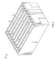
- FIG. 1is a perspective view of an exemplary embodiment of an electrical connector 10 for interconnecting electrical components (not shown), such as, but not limited to, two circuit boards.
- the connector 10includes a dielectric housing 12 having a forward mating end 14 that includes a shroud 16 and a mating face 18 .
- the mating face 18includes a plurality of mating contacts 20 arranged along the mating face 18 , such as, but not limited to, contacts within contact cavities 22 , that are configured to receive corresponding mating contacts (not shown) from a mating connector (not shown) that may be, for example, mounted on a circuit board.
- the shroud 16includes an upper surface 24 and a lower surface 26 between opposite sides 28 .
- the upper and lower surfaces 24 and 26each includes an optional chamfered forward edge portion 30 .
- the sides 28each include optional chamfered side edge portions 32 .
- an alignment rib 34is formed on the upper shroud surface 24 and lower shroud surface 26 . The chamfered edge portions 30 and 32 and the alignment ribs 34 cooperate to bring the connector 10 into alignment with the mating connector during the mating process so that the contacts in the mating connector are received in the contact cavities 22 without damage.
- a plurality of contact modules 36are received in the housing 12 from a rearward end 38 .
- the contact modules 36define a connector mounting face 40 .
- a combination of the housing 12 and a dielectric body 54 of each of the contact modules 36may be referred to herein as a “housing” of the electrical connector 10 , wherein the “housing” includes the mounting face 40 .
- the connector mounting face 40includes a plurality of mounting contacts 42 arranged therealong.
- the mounting contacts 42are configured to be mounted to a substrate (not shown), such as, but not limited to, a circuit board.
- the mounting face 40is approximately perpendicular to the mating face 18 such that the connector 10 interconnects electrical components that are approximately at a right angle to one another.
- the mounting face 40may be angled at any other suitable angle relative to the mating face 18 that enables the connector 10 to interconnect electrical components that are oriented at any other angle relative to each other.
- the housing 12may hold any number of contact modules 36 overall. Each contact module 36 have any number of the mating contacts 20 and any number of the mounting contacts 42 .
- FIG. 2is a perspective view of the housing 12 .
- the housing 12includes a plurality of dividing walls 46 that define a plurality of chambers 48 .
- the chambers 48receive a forward portion of the contact modules 36 ( FIGS. 1 , 3 , and 4 ).
- the chambers 48stabilize the contact modules 36 when the contact modules 36 are loaded into the housing 12 .
- the chambers 48each have about an equal width. However, one or more of the chambers 48 may different widths for accommodating differently sized contact modules 36 .
- each contact module 36includes a lead frame 70 that includes a plurality of electrical terminals 72 .
- the terminals 72extend along predetermined paths to electrically connect each mating contact 20 with each mounting contact 42 .
- Each terminal 72may be either a signal terminal, a ground terminal, or a power terminal.
- the terminals 72are arranged in differential pairs.
- the lead frame 70is encased, or surrounded, in a dielectric body 54 .
- the body 54extends between a mating edge portion 78 and a mounting edge portion 80 that defines a portion of the mounting face 40 .
- the mating contacts 20extend from the mating edge portion 78 of the body 54 and the mounting contacts 42 extend from the mounting edge portion 80 of the body 54 .
- the mounting edge portion 80is approximately perpendicular to the mating edge portion 78 such that the connector 10 interconnects electrical components that are approximately at a right angle to one another.
- the mounting edge portion 80may be angled at any other suitable angle relative to the mating edge portion 78 that enables the connector 10 to interconnect electrical components that are oriented at any other angle relative to each other.
- the lead frames 70 of the receptacle connector 10may be held by a single housing (not shown), which may be integral with, or alternatively held by, the housing 12 .
- FIG. 3is a plan view illustrating an exemplary embodiment of a pattern 82 of the mounting contacts 42 along the mounting face 40 of the connector 10 ( FIG. 1 ) and a pattern 84 of the mating contacts 20 along the mating face 18 of the connector 10 .
- the pattern 82matches the pattern (not shown) of a plurality of vias (not shown) or electrical contacts (not shown) of the electrical component (not shown) electrically connected to the mounting contacts 42 .
- the pattern 84matches the pattern (not shown) of a plurality of vias (not shown) or electrical contacts (not shown) of the electrical component (not shown) electrically connected to the mating contacts 20 .
- the pattern 82includes a plurality of the mounting contacts 42 arranged in differential pairs 86 .
- the differential pairs 86 of mounting contacts 42are arranged in columns that are separated by ground contacts 88 .
- the pattern 84includes a plurality of the mating contacts 20 arranged in differential pairs 90 .
- the differential pairs 90 of mating contacts 20are arranged in columns that are separated by ground contacts 92 .
- Each mounting contact 42 1-12 within the pattern 82is electrically connected to a respective one of the mating contacts 20 1-12 within the pattern 84 via a corresponding terminal 72 (not shown in FIG. 3 ).
- each differential pair 86 of mounting contacts 42one of the two corresponding terminals 72 is selected as a positive terminal 72 while the other terminal 72 is selected as a negative terminal 72 . Accordingly, within each differential pair 86 of the mounting contacts 42 , one of the mounting contacts 42 is a positive mounting contact 42 while the other is a negative mounting contact 42 . Similarly, within each differential pair 90 of mating contacts 20 , the mating contact 20 connected to the corresponding positive terminal 72 is a positive mating contact 20 while the mating contact 20 connected to the corresponding negative terminal 72 is a negative mating contact 20 .
- the pattern 82 of the differential pairs 86 of mounting contacts 42includes two different groups 86 a and 86 b of differential pairs 86 .
- the positive and negative mounting contacts 42 of each differential pair 86 within the group 86 aare aligned along a line 94
- the positive and negative mounting contacts 42 of each differential pair 86 within the group 86 bare aligned along a line 96 .
- the lines 94 of the differential pair group 86 aextend parallel to one another, as do each of the lines 96 of the differential pair group 86 b .
- each of the lines 94is approximately perpendicular to the each of the lines 96 such that the positive and negative mounting contacts 42 of each differential pair 86 within the group 86 a are aligned approximately perpendicular to the positive and negative mounting contacts 42 of each differential pair within the group 86 b . Accordingly, each of the differential pairs 86 within the differential pair group 86 a is aligned approximately perpendicular to each of the differential pairs 86 within the differential pair group 86 b.
- the pattern 84 of the differential pairs 90 of mating contacts 20includes two different groups 90 a and 90 b of differential pairs 90 .
- the positive and negative mating contacts 20 of each differential pair 90 within the group 90 aare aligned along a line 98
- the positive and negative mating contacts 20 of each differential pair 90 within the group 90 bare aligned along a line 100 .
- the lines 98 of the differential pair group 90 aextend parallel to one another, as do each of the lines 100 of the differential pair group 90 b .
- each of the lines 98is approximately perpendicular to the each of the lines 100 such that the positive and negative mating contacts 20 of each differential pair 90 within the group 90 a are aligned approximately perpendicular to the positive and negative mating contacts 20 of each differential pair within the group 90 b . Accordingly, each of the differential pairs 90 within the differential pair group 90 a is aligned approximately perpendicular to each of the differential pairs 90 within the differential pair group 90 b.
- Each differential pair 86 of mounting contacts 42 within the group 86 ahas a common orientation along the mounting face 40 with the corresponding differential pair 90 of mating contacts 20 within the group 90 a has along the mating face 18 .
- the positive and negative mounting contacts 42 of each differential pair 86 within the group 86 awill have a common orientation with the positive and negative mating contacts 20 of the corresponding differential pair 90 within the group 90 a .
- the positive mounting contact 42 1 and the negative mounting contact 42 2have a common orientation along the mounting face 40 with the positive mating contact 20 1 and the negative mating contact 20 2 along the mating face 18
- the positive mounting contact 42 3 and the negative mounting contact 42 4have a common orientation along the mounting face 40 with the positive mating contact 20 3 and the negative mating contact 20 4 along the mating face 18
- the positive mounting contact 42 5 and the negative mounting contact 42 6have a common orientation along the mounting face 40 with the positive mating contact 20 5 and the negative mating contact 20 6 along the mating face 18 .
- Each differential pair 86 of mounting contacts 42 within the group 86 bhas a different orientation along the mounting face 40 than the corresponding differential pair 90 of mating contacts 20 within the group 90 b has along the mating face 18 .
- the orientation of the positive and negative mounting contacts 42 of each differential pair 86 within the group 86 bis inverted approximately 180° relative to the positive and negative mating contacts 20 of the corresponding differential pair 90 within the group 90 b .
- the orientation of the positive mounting contact 42 7 and the negative mounting contact 42 8 along the mounting face 40is inverted relative to the orientation of the positive mating contact 20 7 and the negative mating contact 20 8 along the mating face 18
- the orientation of the positive mounting contact 42 9 and the negative mounting contact 42 10 along the mounting face 40is inverted relative to the orientation of the positive mating contact 20 9 and the negative mating contact 20 10 along the mating face 18
- the orientation of the positive mounting contact 42 11 and the negative mounting contact 42 12 along the mounting face 40is inverted relative to the orientation of the positive mating contact 20 11 and the negative mating contact 20 12 along the mating face 18 .
- Inverting the orientation of the differential pairs 86 within the group 86 b on the mounting face 40 relative to the corresponding differential pairs 90 within the group 90 b on the mating face 18may facilitate reducing overall far-end crosstalk generated by the two footprints on either side of the electrical connector 10 .
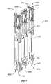
- FIG. 4is a perspective view of an exemplary embodiment of a lead frame 170 that may be used with one of the contact modules 36 to generate patterns similar to the patterns 82 and 84 ( FIG. 3 ).
- the lead frame 170includes a plurality of mounting contacts 142 , a plurality of the mating contacts 120 , and a plurality of terminals 172 .
- Each terminal 172interconnects a mounting contact 142 with the corresponding mating contact 120 .
- Each of the mating contacts 120is optionally connected to the corresponding terminal 172 via a connector 173 , as shown in the exemplary embodiment of FIG. 4 .
- each of the mounting contacts 142is optionally connected to the corresponding terminal 172 via a connector (not shown).
- the terminals 172are arranged in differential pairs. Accordingly, the mounting and mating contacts 142 and 120 , respectively, are arranged in differential pairs 186 and 190 , respectively. Within each differential pair, one terminal 172 is selected as a positive terminal 172 while the other terminal 172 is selected as a negative terminal 172 . Accordingly, within each differential pair 186 , one mounting contacts 142 is a positive mounting contact 142 while the other is a negative mounting contact 142 . Similarly, within each differential pair 190 , one mating contact 120 is a positive mating contact 120 while the other is a negative mating contact 120 .
- the differential pairs 186 of mounting contacts 142include two different groups 186 a and 186 b of differential pairs 186 . As can be seen in FIG.
- each of the differential pairs 186 within the differential pair group 186 ais aligned approximately perpendicular to each of the differential pairs 186 within the differential pair group 186 b .
- the differential pairs 190 of mating contacts 120include two different groups 190 a and 190 b of differential pairs 190 .
- Each of the differential pairs 190 within the differential pair group 190 ais aligned approximately perpendicular to each of the differential pairs 190 within the differential pair group 190 b.
- Each differential pair 186 of mounting contacts 142 within the group 186 ahas a common orientation with the corresponding differential pair 190 of mating contacts 120 within the group 190 a .
- each differential pair 186 of mounting contacts 142 within the group 186 bhas a different orientation than the corresponding differential pair 190 of mating contacts 120 within the group 190 b.
- the orientation of the positive and negative mounting contacts 142 of each differential pair 186 within the group 186 bis inverted relative to the positive and negative mating contacts 120 of the corresponding differential pair 190 within the group 190 b .
- the orientation of the positive mounting contact 142 9 and the negative mounting contact 142 10is inverted relative to the orientation of the positive mating contact 120 9 and the negative mating contact 120 10
- the orientation of the positive mounting contact 142 11 and the negative mounting contact 142 12is inverted relative to the orientation of the positive mating contact 120 11 and the negative mating contact 120 12
- the orientation of the positive mounting contact 142 13 and the negative mounting contact 142 14is inverted relative to the orientation of the positive mating contact 120 13 and the negative mating contact 120 14
- the orientation of the positive mounting contact 142 15 and the negative mounting contact 142 16is inverted relative to the orientation of the positive mating contact 120 15 and the negative mating contact 120 16 .
- the mounting contacts 142 , the mating contacts 120 , and/or the terminals 172 of the differential pair group 186 binclude geometry that provides the corresponding mounting contacts 142 and mating contacts 120 of the differential pair group 186 b with the inverted orientation.
- a positive terminal 172 + of each differential pair of the group 186 bincludes an angled portion 175 adjacent the corresponding mounting contact 142 and an angled portion 177 adjacent the corresponding mating contact 120 that each facilitate the inverted orientation.
- a negative terminal 172 ⁇ of each differential pair of the group 186 bincludes an angled portion 179 adjacent the corresponding mating contact 120 that facilitates the inverted orientation.
- any of the mating contacts 120 , the mounting contacts 142 , and/or the terminals 172may include the geometry that facilitates providing the inverted orientation.
- the geometry that facilitates providing the inverted orientationmay be at any location(s) along the mating contacts 120 , the mounting contacts 142 , and/or the terminals 172 that enables the inverted orientation.
- FIG. 5is a plan view illustrating an exemplary embodiment of a pattern 282 of mounting contacts 242 that may extend from the mounting face 40 of the connector 10 ( FIG. 1 ) and a pattern 284 of mating contacts 220 that may extend from the mating face 18 of the connector 10 .
- the pattern 282matches the pattern (not shown) of a plurality of vias (not shown) or electrical contacts (not shown) of the electrical component (not shown) electrically connected to the mounting contacts 242 .
- the pattern 284matches the pattern (not shown) of a plurality of vias (not shown) or electrical contacts (not shown) of the electrical component (not shown) electrically connected to the mating contacts 220 .
- the pattern 282includes a plurality of the mounting contacts 242 arranged in differential pairs 286 .
- the pattern 284includes a plurality of the mating contacts 220 arranged in differential pairs 290 .
- Each mounting contact 242 1-16 within the pattern 282is electrically connected to a respective one of the mating contacts 220 1-16 within the pattern 284 via a corresponding terminal (not shown).
- one of the mounting contacts 242is a positive mounting contact 242 while the other is a negative mounting contact 242 .
- one of the mating contacts 220is a positive mating contact 220 while the other mating contact 220 is a negative mating contact 220 .
- the pattern 282 of the differential pairs 286 of mounting contacts 242includes two different groups 286 a and 286 b of differential pairs 286 . Each of the differential pairs 286 within the differential pair group 286 a is aligned approximately perpendicular to each of the differential pairs 286 within the differential pair group 286 b.
- the pattern 284 of the differential pairs 290 of mating contacts 220includes two different groups 290 a and 290 b of differential pairs 290 . Each of the differential pairs 290 within the differential pair group 290 a is aligned approximately perpendicular to each of the differential pairs 290 within the differential pair group 290 b.
- the orientation of the positive and negative mounting contacts 242 of each differential pair 286 within the group 286 bis inverted relative to the positive and negative mating contacts 220 of the corresponding differential pair 290 within the group 290 b .
- the orientation of the positive and negative mounting contacts 242 of each differential pair 286 within the group 286 ais inverted relative to the positive and negative mating contacts 220 of the corresponding differential pair 290 within the group 290 a.
- FIG. 6is a plan view illustrating an exemplary embodiment of a pattern 382 of mounting contacts 342 that may extend from the mounting face 40 of the connector 10 ( FIG. 1 ) and a pattern 384 of mating contacts 320 that may extend from the mating face 18 of the connector 10 .
- the pattern 382matches the pattern (not shown) of a plurality of vias (not shown) or electrical contacts (not shown) of the electrical component (not shown) electrically connected to the mounting contacts 342 .
- the pattern 384matches the pattern (not shown) of a plurality of vias (not shown) or electrical contacts (not shown) of the electrical component (not shown) electrically connected to the mating contacts 320 .
- the pattern 382includes a plurality of the mounting contacts 342 arranged in differential pairs 386 .
- the differential pairs 386 of the mounting contacts 342are arranged in rows that are separated by ground contacts 388 .
- the pattern 384includes a plurality of the mating contacts 320 arranged in differential pairs 390 .
- the differential pairs 390 of mating contacts 320are arranged in rows that are separated by ground contacts 392 .
- Each mounting contact 342 1-16 within the pattern 382is electrically connected to a respective one of the mating contacts 320 1-16 within the pattern 384 via a corresponding terminal (not shown).
- one of the mounting contacts 342is a positive mounting contact 342 while the other is a negative mounting contact 342 .
- one of the mating contacts 320is a positive mating contact 320 while the other mating contact 320 is a negative mating contact 320 .
- the pattern 382 of the differential pairs 386 of mounting contacts 342includes two different groups 386 a and 386 b of differential pairs 386 . Each of the differential pairs 386 within the differential pair group 386 a is aligned approximately parallel to each of the differential pairs 386 within the differential pair group 386 b.
- the pattern 384 of the differential pairs 390 of mating contacts 320includes two different groups 390 a and 390 b of differential pairs 390 . Each of the differential pairs 390 within the differential pair group 390 a is aligned approximately parallel to each of the differential pairs 390 within the differential pair group 390 b.
- Each differential pair 386 of mounting contacts 342 within the group 386 ahas a common orientation with the corresponding differential pair 390 of mating contacts 320 within the group 390 a .
- the positive and negative mounting contacts 342 of each differential pair 386 within the group 386 awill have a common orientation with the positive and negative mating contacts 320 of the corresponding differential pair 390 within the group 390 a.
- the orientation of the positive and negative mounting contacts 342 of each differential pair 386 within the group 386 bis inverted relative to the positive and negative mating contacts 320 of the corresponding differential pair 390 within the group 390 b .
- the orientation of the positive and negative mounting contacts 342 of each differential pair 386 within the group 386 ais inverted relative to the positive and negative mating contacts 320 of the corresponding differential pair 390 within the group 390 a.
- connector 10is described and illustrated herein with particular reference to a receptacle connector, it is to be understood that the benefits herein described are also applicable to other connectors in other embodiments.
- the description and illustration hereinis therefore provided for purposes of illustration, rather than limitation, and is but one potential application of the subject matter described and/or illustrated herein.
- FIG. 7is a perspective view of an exemplary embodiment of a lead frame 470 that may be used with one of the contact modules 36 to generate patterns similar to the patterns 82 and 84 ( FIG. 3 ).
- the lead frame 470is configured to interconnect electrical components, such as, but not limited to, circuit boards, that are oriented approximately parallel to each other.
- the lead frame 470includes a plurality of mounting contacts 442 , a plurality of the mating contacts 420 , and a plurality of terminals 472 .
- Each terminal 472interconnects a mounting contact 442 with the corresponding mating contact 420 .
- Each of the mating contacts 420 and each of the mounting contacts 442is optionally connected to the corresponding terminal 472 via a connector (not shown).
- the terminals 472are arranged in differential pairs. Accordingly, the mounting and mating contacts 442 and 420 , respectively, are arranged in differential pairs 486 and 490 , respectively. Within each differential pair, one terminal 472 is selected as a positive terminal 472 while the other terminal 472 is selected as a negative terminal 472 .
- one mounting contacts 442is a positive mounting contact 442 while the other is a negative mounting contact 442 .
- one mating contact 420is a positive mating contact 420 while the other is a negative mating contact 420 .
- the differential pairs 486 of mounting contacts 442include two different groups 486 a and 486 b of differential pairs 486 . Each of the differential pairs 486 within the differential pair group 486 a is aligned approximately perpendicular to each of the differential pairs 486 within the differential pair group 486 b .
- the differential pairs 490 of mating contacts 420include two different groups 490 a and 490 b of differential pairs 490 . Each of the differential pairs 490 within the differential pair group 490 a is aligned approximately perpendicular to each of the differential pairs 490 within the differential pair group 490 b.
- Each differential pair 486 of mounting contacts 442 within the group 486 ahas a common orientation with the corresponding differential pair 490 of mating contacts 420 within the group 490 a .
- the orientation of the positive and negative mounting contacts 442 of each differential pair 486 within the group 486 bis inverted relative to the positive and negative mating contacts 420 of the corresponding differential pair 490 within the group 490 a.
- the mounting contacts 442 , the mating contacts 420 , and/or the terminals 472 of the differential pair group 486 binclude geometry that provides the corresponding mounting contacts 442 and mating contacts 420 of the differential pair group 486 b with the inverted orientation.
- a negative terminal 472 ⁇ of each differential pair of the group 486 binclude an angled portion 475 adjacent the corresponding mounting contact 442 that facilitates the inverted orientation.
- any of the mating contacts 420 , the mounting contacts 442 , and/or the terminals 472may include the geometry that facilitates providing the inverted orientation.
- the geometry that facilitates providing the inverted orientationmay be at any location(s) along the mating contacts 420 , the mounting contacts 442 , and/or the terminals 472 that enables the inverted orientation.
- the mounting contacts 42 , 142 , and 442may each be any suitable type of electrical contact that enables the mounting contacts 42 , 142 , and 442 to function as described herein, such as, but not limited to, a press-fit type, a surface mount type, and/or a solder tail type.
- the mating contacts 20 , 120 , and 420may each be any suitable type of electrical contact that enables the mating contacts 20 , 120 , and 420 to function as described herein, such as, but not limited to, a press-fit type, a surface mount type, and/or a solder tail type.
- the electrical connector 10is described herein as interconnecting two electrical components using both the electrical connector 10 and a mating connector mounted on one of the electrical components, alternatively the electrical connector 10 directly interconnects the two electrical components without the mating connector intervening between one of the electrical components and the electrical connector 10 .
- inventions described and/or illustrated hereinprovide an electrical interconnection that may reduce far-end crosstalk generated by two circuit board footprints on either side of an electrical connector without reducing impedance, decreasing signal density, and/or increasing cost.
Landscapes
- Details Of Connecting Devices For Male And Female Coupling (AREA)
- Coupling Device And Connection With Printed Circuit (AREA)
Abstract
Description
Claims (20)
Priority Applications (4)
| Application Number | Priority Date | Filing Date | Title |
|---|---|---|---|
| US12/188,961US7862344B2 (en) | 2008-08-08 | 2008-08-08 | Electrical connector having reversed differential pairs |
| EP09789039.6AEP2324541B1 (en) | 2008-08-08 | 2009-07-30 | Electrical connector having reversed differential pairs |
| CN200980130336.7ACN102113179B (en) | 2008-08-08 | 2009-07-30 | Electrical connector with reverse differential pair |
| PCT/US2009/004398WO2010016874A1 (en) | 2008-08-08 | 2009-07-30 | Electrical connector having reversed differential pairs |
Applications Claiming Priority (1)
| Application Number | Priority Date | Filing Date | Title |
|---|---|---|---|
| US12/188,961US7862344B2 (en) | 2008-08-08 | 2008-08-08 | Electrical connector having reversed differential pairs |
Publications (2)
| Publication Number | Publication Date |
|---|---|
| US20100035454A1 US20100035454A1 (en) | 2010-02-11 |
| US7862344B2true US7862344B2 (en) | 2011-01-04 |
Family
ID=41174900
Family Applications (1)
| Application Number | Title | Priority Date | Filing Date |
|---|---|---|---|
| US12/188,961Active2029-01-23US7862344B2 (en) | 2008-08-08 | 2008-08-08 | Electrical connector having reversed differential pairs |
Country Status (4)
| Country | Link |
|---|---|
| US (1) | US7862344B2 (en) |
| EP (1) | EP2324541B1 (en) |
| CN (1) | CN102113179B (en) |
| WO (1) | WO2010016874A1 (en) |
Cited By (37)
| Publication number | Priority date | Publication date | Assignee | Title |
|---|---|---|---|---|
| US20110207342A1 (en)* | 2010-02-24 | 2011-08-25 | Wayne Samuel Davis | Increased density connector system |
| US20130005160A1 (en)* | 2011-07-01 | 2013-01-03 | Fci Americas Technology Llc | Connection Footprint For Electrical Connector With Printed Wiring Board |
| US8449330B1 (en)* | 2011-12-08 | 2013-05-28 | Tyco Electronics Corporation | Cable header connector |
| US20140057493A1 (en)* | 2012-08-27 | 2014-02-27 | Jan De Geest | High speed electrical connector |
| US20140111960A1 (en)* | 2012-10-23 | 2014-04-24 | Tyco Electronics Corporation | Leadframe module for an electrical connector |
| US20140154927A1 (en)* | 2012-11-30 | 2014-06-05 | Hitachi Cable, Ltd. | Cable connector and cable assembly, and method of manufacturing cable assembly |
| US20140242844A1 (en)* | 2013-02-27 | 2014-08-28 | Molex Incorporated | High Speed Bypass Cable For Use With Backplanes |
| US9011177B2 (en) | 2009-01-30 | 2015-04-21 | Molex Incorporated | High speed bypass cable assembly |
| US9142921B2 (en) | 2013-02-27 | 2015-09-22 | Molex Incorporated | High speed bypass cable for use with backplanes |
| US20160036165A1 (en)* | 2014-07-29 | 2016-02-04 | Tyco Electronics Corporation | High speed signal-isolating electrical connector assembly |
| US9413112B2 (en)* | 2014-08-07 | 2016-08-09 | Tyco Electronics Corporation | Electrical connector having contact modules |
| US9520661B1 (en)* | 2015-08-25 | 2016-12-13 | Tyco Electronics Corporation | Electrical connector assembly |
| US20170077621A1 (en)* | 2015-09-15 | 2017-03-16 | Foxconn Interconnect Technology Limited | Electrical connector |
| US10062984B2 (en) | 2013-09-04 | 2018-08-28 | Molex, Llc | Connector system with cable by-pass |
| US10135211B2 (en) | 2015-01-11 | 2018-11-20 | Molex, Llc | Circuit board bypass assemblies and components therefor |
| US10367280B2 (en) | 2015-01-11 | 2019-07-30 | Molex, Llc | Wire to board connectors suitable for use in bypass routing assemblies |
| US10424856B2 (en) | 2016-01-11 | 2019-09-24 | Molex, Llc | Routing assembly and system using same |
| US10424878B2 (en) | 2016-01-11 | 2019-09-24 | Molex, Llc | Cable connector assembly |
| US10468823B2 (en)* | 2017-10-26 | 2019-11-05 | Foxconn (Kunshan) Computer Connector Co., Ltd. | Electrical connector having improved contacts structure |
| US10720735B2 (en) | 2016-10-19 | 2020-07-21 | Amphenol Corporation | Compliant shield for very high speed, high density electrical interconnection |
| US10739828B2 (en) | 2015-05-04 | 2020-08-11 | Molex, Llc | Computing device using bypass assembly |
| US10840649B2 (en) | 2014-11-12 | 2020-11-17 | Amphenol Corporation | Organizer for a very high speed, high density electrical interconnection system |
| US10931062B2 (en) | 2018-11-21 | 2021-02-23 | Amphenol Corporation | High-frequency electrical connector |
| US11070006B2 (en) | 2017-08-03 | 2021-07-20 | Amphenol Corporation | Connector for low loss interconnection system |
| US11101611B2 (en) | 2019-01-25 | 2021-08-24 | Fci Usa Llc | I/O connector configured for cabled connection to the midboard |
| US11151300B2 (en) | 2016-01-19 | 2021-10-19 | Molex, Llc | Integrated routing assembly and system using same |
| US11189943B2 (en) | 2019-01-25 | 2021-11-30 | Fci Usa Llc | I/O connector configured for cable connection to a midboard |
| US11205877B2 (en) | 2018-04-02 | 2021-12-21 | Ardent Concepts, Inc. | Controlled-impedance compliant cable termination |
| US11437762B2 (en) | 2019-02-22 | 2022-09-06 | Amphenol Corporation | High performance cable connector assembly |
| US11444398B2 (en) | 2018-03-22 | 2022-09-13 | Amphenol Corporation | High density electrical connector |
| US11469553B2 (en) | 2020-01-27 | 2022-10-11 | Fci Usa Llc | High speed connector |
| US11522310B2 (en) | 2012-08-22 | 2022-12-06 | Amphenol Corporation | High-frequency electrical connector |
| US11670879B2 (en) | 2020-01-28 | 2023-06-06 | Fci Usa Llc | High frequency midboard connector |
| US11735852B2 (en) | 2019-09-19 | 2023-08-22 | Amphenol Corporation | High speed electronic system with midboard cable connector |
| US11799246B2 (en) | 2020-01-27 | 2023-10-24 | Fci Usa Llc | High speed connector |
| USD1002553S1 (en) | 2021-11-03 | 2023-10-24 | Amphenol Corporation | Gasket for connector |
| US11831106B2 (en) | 2016-05-31 | 2023-11-28 | Amphenol Corporation | High performance cable termination |
Families Citing this family (23)
| Publication number | Priority date | Publication date | Assignee | Title |
|---|---|---|---|---|
| US8500487B2 (en)* | 2011-11-15 | 2013-08-06 | Tyco Electronics Corporation | Grounding structures for header and receptacle assemblies |
| US9407043B2 (en) | 2012-07-16 | 2016-08-02 | Commscope, Inc. Of North Carolina | Balanced pin and socket connectors |
| US8905791B2 (en)* | 2013-02-15 | 2014-12-09 | Continental Automotive Systems, Inc. | Single layer leadframe with integrated three-row connector |
| US9276386B2 (en)* | 2013-02-15 | 2016-03-01 | Continental Automotive Systems, Inc. | Single layer leadframe with integrated three-row connector |
| TWD163690S (en)* | 2013-09-06 | 2014-10-21 | 通普康電子(昆山)有限公司; | Electrical connector parts |
| TWD163691S (en)* | 2013-09-06 | 2014-10-21 | 通普康電子(昆山)有限公司; | Parts of electrical connectors |
| CN104182576B (en)* | 2014-08-20 | 2017-05-03 | 浪潮电子信息产业股份有限公司 | Design method for reducing crosstalk influence between high-speed differential pairs |
| GB2547958B (en) | 2016-03-04 | 2019-12-18 | Commscope Technologies Llc | Two-wire plug and receptacle |
| CN110233395B (en)* | 2016-11-30 | 2021-03-23 | 中航光电科技股份有限公司 | Differential connector and its differential pair arrangement, differential connector plug |
| MX2019011906A (en) | 2017-04-24 | 2019-11-25 | Commscope Technologies Llc | Connectors for a single twisted pair of conductors. |
| WO2018227057A1 (en) | 2017-06-08 | 2018-12-13 | Commscope Technologies Llc | Connectors for a single twisted pair of conductors |
| WO2019147774A1 (en) | 2018-01-26 | 2019-08-01 | Commscope Technologies Llc | Connectors for a single twisted pair of conductors |
| CN115313074A (en) | 2018-02-26 | 2022-11-08 | 康普技术有限责任公司 | Electrical contact for two wire connector only |
| US11157213B2 (en) | 2018-10-12 | 2021-10-26 | Micron Technology, Inc. | Parallel memory access and computation in memory devices |
| US10461076B1 (en) | 2018-10-24 | 2019-10-29 | Micron Technology, Inc. | 3D stacked integrated circuits having functional blocks configured to accelerate artificial neural network (ANN) computation |
| WO2020190758A1 (en) | 2019-03-15 | 2020-09-24 | Commscope Technologies Llc | Connectors and contacts for a single twisted pair of conductors |
| US12327948B2 (en) | 2019-09-30 | 2025-06-10 | Commscope Technologies Llc | High density coupling panel |
| WO2021067274A1 (en) | 2019-09-30 | 2021-04-08 | Commscope Technologies Llc | Couplers for single pair connectors |
| US12359193B2 (en) | 2022-03-04 | 2025-07-15 | Element Biosciences, Inc. | Single-stranded splint strands and methods of use |
| US12371743B2 (en) | 2022-03-04 | 2025-07-29 | Element Biosciences, Inc. | Double-stranded splint adaptors and methods of use |
| CN114628958B (en)* | 2021-02-09 | 2024-04-16 | 中航光电科技股份有限公司 | Differential signal module and differential signal connector |
| US12199372B2 (en) | 2021-02-26 | 2025-01-14 | Commscope Technologies Llc | Couplers for single pair connectors |
| JP2025530259A (en) | 2022-09-12 | 2025-09-11 | エレメント バイオサイエンシズ,インコーポレイティド | Dual-stranded splint adapter with universal long splint strand and method of use |
Citations (7)
| Publication number | Priority date | Publication date | Assignee | Title |
|---|---|---|---|---|
| WO2001039332A1 (en) | 1999-11-24 | 2001-05-31 | Teradyne, Inc. | Differential signal electrical connectors |
| US6554647B1 (en)* | 1997-02-07 | 2003-04-29 | Teradyne, Inc. | Differential signal electrical connectors |
| EP1347539A1 (en) | 2002-03-12 | 2003-09-24 | Albert Ackermann GmbH & Co. KG | Electrical connector for the data technology |
| DE102005057905A1 (en) | 2004-12-02 | 2006-06-08 | Tyco Electronics Corp. | Noise eliminating differential connector and footprint arrangement of this |
| US7255573B2 (en)* | 2005-12-30 | 2007-08-14 | Intel Corporation | Data signal interconnection with reduced crosstalk |
| US7309257B1 (en) | 2006-06-30 | 2007-12-18 | Fci Americas Technology, Inc. | Hinged leadframe assembly for an electrical connector |
| US20090068887A1 (en)* | 2007-08-03 | 2009-03-12 | Yamaichi Electronics Co., Ltd | High speed transmission connector |
- 2008
- 2008-08-08USUS12/188,961patent/US7862344B2/enactiveActive
- 2009
- 2009-07-30EPEP09789039.6Apatent/EP2324541B1/enactiveActive
- 2009-07-30WOPCT/US2009/004398patent/WO2010016874A1/enactiveApplication Filing
- 2009-07-30CNCN200980130336.7Apatent/CN102113179B/enactiveActive
Patent Citations (8)
| Publication number | Priority date | Publication date | Assignee | Title |
|---|---|---|---|---|
| US6554647B1 (en)* | 1997-02-07 | 2003-04-29 | Teradyne, Inc. | Differential signal electrical connectors |
| WO2001039332A1 (en) | 1999-11-24 | 2001-05-31 | Teradyne, Inc. | Differential signal electrical connectors |
| EP1347539A1 (en) | 2002-03-12 | 2003-09-24 | Albert Ackermann GmbH & Co. KG | Electrical connector for the data technology |
| DE102005057905A1 (en) | 2004-12-02 | 2006-06-08 | Tyco Electronics Corp. | Noise eliminating differential connector and footprint arrangement of this |
| US7207807B2 (en) | 2004-12-02 | 2007-04-24 | Tyco Electronics Corporation | Noise canceling differential connector and footprint |
| US7255573B2 (en)* | 2005-12-30 | 2007-08-14 | Intel Corporation | Data signal interconnection with reduced crosstalk |
| US7309257B1 (en) | 2006-06-30 | 2007-12-18 | Fci Americas Technology, Inc. | Hinged leadframe assembly for an electrical connector |
| US20090068887A1 (en)* | 2007-08-03 | 2009-03-12 | Yamaichi Electronics Co., Ltd | High speed transmission connector |
Non-Patent Citations (1)
| Title |
|---|
| International Search Report, International Application No. PCT/US2009/004398, International Filing Date Jul. 30, 2009. |
Cited By (87)
| Publication number | Priority date | Publication date | Assignee | Title |
|---|---|---|---|---|
| USRE48230E1 (en) | 2009-01-30 | 2020-09-29 | Molex, Llc | High speed bypass cable assembly |
| USRE47342E1 (en) | 2009-01-30 | 2019-04-09 | Molex, Llc | High speed bypass cable assembly |
| US9011177B2 (en) | 2009-01-30 | 2015-04-21 | Molex Incorporated | High speed bypass cable assembly |
| US8371876B2 (en)* | 2010-02-24 | 2013-02-12 | Tyco Electronics Corporation | Increased density connector system |
| US20110207342A1 (en)* | 2010-02-24 | 2011-08-25 | Wayne Samuel Davis | Increased density connector system |
| US8920194B2 (en)* | 2011-07-01 | 2014-12-30 | Fci Americas Technology Inc. | Connection footprint for electrical connector with printed wiring board |
| US20130005160A1 (en)* | 2011-07-01 | 2013-01-03 | Fci Americas Technology Llc | Connection Footprint For Electrical Connector With Printed Wiring Board |
| US8449330B1 (en)* | 2011-12-08 | 2013-05-28 | Tyco Electronics Corporation | Cable header connector |
| US11901663B2 (en) | 2012-08-22 | 2024-02-13 | Amphenol Corporation | High-frequency electrical connector |
| US11522310B2 (en) | 2012-08-22 | 2022-12-06 | Amphenol Corporation | High-frequency electrical connector |
| US9515429B2 (en)* | 2012-08-27 | 2016-12-06 | FCI Asia Pte. Ltd. | High speed electrical connector |
| US20140057493A1 (en)* | 2012-08-27 | 2014-02-27 | Jan De Geest | High speed electrical connector |
| US10038282B2 (en) | 2012-08-27 | 2018-07-31 | Amphenol Fci Asia Pte. Ltd. | High speed electrical connector |
| US9093800B2 (en)* | 2012-10-23 | 2015-07-28 | Tyco Electronics Corporation | Leadframe module for an electrical connector |
| US20140111960A1 (en)* | 2012-10-23 | 2014-04-24 | Tyco Electronics Corporation | Leadframe module for an electrical connector |
| US8900007B2 (en)* | 2012-11-30 | 2014-12-02 | Hitachi Metals, Ltd. | Cable connector and cable assembly, and method of manufacturing cable assembly |
| US20140154927A1 (en)* | 2012-11-30 | 2014-06-05 | Hitachi Cable, Ltd. | Cable connector and cable assembly, and method of manufacturing cable assembly |
| US10305204B2 (en) | 2013-02-27 | 2019-05-28 | Molex, Llc | High speed bypass cable for use with backplanes |
| US10056706B2 (en) | 2013-02-27 | 2018-08-21 | Molex, Llc | High speed bypass cable for use with backplanes |
| US20140242844A1 (en)* | 2013-02-27 | 2014-08-28 | Molex Incorporated | High Speed Bypass Cable For Use With Backplanes |
| US9362678B2 (en) | 2013-02-27 | 2016-06-07 | Molex, Llc | Connection system for use with a chip |
| US10069225B2 (en) | 2013-02-27 | 2018-09-04 | Molex, Llc | High speed bypass cable for use with backplanes |
| US8845364B2 (en)* | 2013-02-27 | 2014-09-30 | Molex Incorporated | High speed bypass cable for use with backplanes |
| US9608348B2 (en) | 2013-02-27 | 2017-03-28 | Molex, Llc | High speed bypass cable for use with backplanes |
| US9490558B2 (en) | 2013-02-27 | 2016-11-08 | Molex, Llc | Connection system for use with a chip |
| US9985367B2 (en) | 2013-02-27 | 2018-05-29 | Molex, Llc | High speed bypass cable for use with backplanes |
| US9257794B2 (en) | 2013-02-27 | 2016-02-09 | Molex, Llc | High speed bypass cable for use with backplanes |
| US9142921B2 (en) | 2013-02-27 | 2015-09-22 | Molex Incorporated | High speed bypass cable for use with backplanes |
| US10062984B2 (en) | 2013-09-04 | 2018-08-28 | Molex, Llc | Connector system with cable by-pass |
| US10181663B2 (en) | 2013-09-04 | 2019-01-15 | Molex, Llc | Connector system with cable by-pass |
| US9559465B2 (en)* | 2014-07-29 | 2017-01-31 | Tyco Electronics Corporation | High speed signal-isolating electrical connector assembly |
| US20160036165A1 (en)* | 2014-07-29 | 2016-02-04 | Tyco Electronics Corporation | High speed signal-isolating electrical connector assembly |
| US9413112B2 (en)* | 2014-08-07 | 2016-08-09 | Tyco Electronics Corporation | Electrical connector having contact modules |
| US11764523B2 (en) | 2014-11-12 | 2023-09-19 | Amphenol Corporation | Very high speed, high density electrical interconnection system with impedance control in mating region |
| US10840649B2 (en) | 2014-11-12 | 2020-11-17 | Amphenol Corporation | Organizer for a very high speed, high density electrical interconnection system |
| US10855034B2 (en) | 2014-11-12 | 2020-12-01 | Amphenol Corporation | Very high speed, high density electrical interconnection system with impedance control in mating region |
| US10367280B2 (en) | 2015-01-11 | 2019-07-30 | Molex, Llc | Wire to board connectors suitable for use in bypass routing assemblies |
| US11621530B2 (en) | 2015-01-11 | 2023-04-04 | Molex, Llc | Circuit board bypass assemblies and components therefor |
| US10135211B2 (en) | 2015-01-11 | 2018-11-20 | Molex, Llc | Circuit board bypass assemblies and components therefor |
| US11114807B2 (en) | 2015-01-11 | 2021-09-07 | Molex, Llc | Circuit board bypass assemblies and components therefor |
| US10637200B2 (en) | 2015-01-11 | 2020-04-28 | Molex, Llc | Circuit board bypass assemblies and components therefor |
| US10784603B2 (en) | 2015-01-11 | 2020-09-22 | Molex, Llc | Wire to board connectors suitable for use in bypass routing assemblies |
| US11003225B2 (en) | 2015-05-04 | 2021-05-11 | Molex, Llc | Computing device using bypass assembly |
| US10739828B2 (en) | 2015-05-04 | 2020-08-11 | Molex, Llc | Computing device using bypass assembly |
| US9520661B1 (en)* | 2015-08-25 | 2016-12-13 | Tyco Electronics Corporation | Electrical connector assembly |
| US20170077621A1 (en)* | 2015-09-15 | 2017-03-16 | Foxconn Interconnect Technology Limited | Electrical connector |
| US9728866B2 (en)* | 2015-09-15 | 2017-08-08 | Foxconn Interconnect Technology Limited | Electrical connector |
| US10797416B2 (en) | 2016-01-11 | 2020-10-06 | Molex, Llc | Routing assembly and system using same |
| US11108176B2 (en) | 2016-01-11 | 2021-08-31 | Molex, Llc | Routing assembly and system using same |
| US11688960B2 (en) | 2016-01-11 | 2023-06-27 | Molex, Llc | Routing assembly and system using same |
| US10424856B2 (en) | 2016-01-11 | 2019-09-24 | Molex, Llc | Routing assembly and system using same |
| US10424878B2 (en) | 2016-01-11 | 2019-09-24 | Molex, Llc | Cable connector assembly |
| US11842138B2 (en) | 2016-01-19 | 2023-12-12 | Molex, Llc | Integrated routing assembly and system using same |
| US11151300B2 (en) | 2016-01-19 | 2021-10-19 | Molex, Llc | Integrated routing assembly and system using same |
| US11831106B2 (en) | 2016-05-31 | 2023-11-28 | Amphenol Corporation | High performance cable termination |
| US11387609B2 (en) | 2016-10-19 | 2022-07-12 | Amphenol Corporation | Compliant shield for very high speed, high density electrical interconnection |
| US10720735B2 (en) | 2016-10-19 | 2020-07-21 | Amphenol Corporation | Compliant shield for very high speed, high density electrical interconnection |
| US11637401B2 (en) | 2017-08-03 | 2023-04-25 | Amphenol Corporation | Cable connector for high speed in interconnects |
| US11824311B2 (en) | 2017-08-03 | 2023-11-21 | Amphenol Corporation | Connector for low loss interconnection system |
| US11070006B2 (en) | 2017-08-03 | 2021-07-20 | Amphenol Corporation | Connector for low loss interconnection system |
| US10468823B2 (en)* | 2017-10-26 | 2019-11-05 | Foxconn (Kunshan) Computer Connector Co., Ltd. | Electrical connector having improved contacts structure |
| US11444398B2 (en) | 2018-03-22 | 2022-09-13 | Amphenol Corporation | High density electrical connector |
| US11677188B2 (en) | 2018-04-02 | 2023-06-13 | Ardent Concepts, Inc. | Controlled-impedance compliant cable termination |
| US11996654B2 (en) | 2018-04-02 | 2024-05-28 | Ardent Concepts, Inc. | Controlled-impedance compliant cable termination |
| US11205877B2 (en) | 2018-04-02 | 2021-12-21 | Ardent Concepts, Inc. | Controlled-impedance compliant cable termination |
| US12368270B2 (en) | 2018-04-02 | 2025-07-22 | Ardent Concepts, Inc. | Controlled-impedance compliant cable termination |
| US10931062B2 (en) | 2018-11-21 | 2021-02-23 | Amphenol Corporation | High-frequency electrical connector |
| US11742620B2 (en) | 2018-11-21 | 2023-08-29 | Amphenol Corporation | High-frequency electrical connector |
| US12218462B2 (en) | 2018-11-21 | 2025-02-04 | Amphenol Corporation | High-frequency electrical connector |
| US11637390B2 (en) | 2019-01-25 | 2023-04-25 | Fci Usa Llc | I/O connector configured for cable connection to a midboard |
| US12362505B2 (en) | 2019-01-25 | 2025-07-15 | Fci Usa Llc | I/O connector configured for cable connection to a midboard |
| US12272917B2 (en) | 2019-01-25 | 2025-04-08 | Fci Usa Llc | I/O connector configured for cabled connection to the midboard |
| US11189943B2 (en) | 2019-01-25 | 2021-11-30 | Fci Usa Llc | I/O connector configured for cable connection to a midboard |
| US11101611B2 (en) | 2019-01-25 | 2021-08-24 | Fci Usa Llc | I/O connector configured for cabled connection to the midboard |
| US11715922B2 (en) | 2019-01-25 | 2023-08-01 | Fci Usa Llc | I/O connector configured for cabled connection to the midboard |
| US11984678B2 (en) | 2019-01-25 | 2024-05-14 | Fci Usa Llc | I/O connector configured for cable connection to a midboard |
| US11437762B2 (en) | 2019-02-22 | 2022-09-06 | Amphenol Corporation | High performance cable connector assembly |
| US11735852B2 (en) | 2019-09-19 | 2023-08-22 | Amphenol Corporation | High speed electronic system with midboard cable connector |
| US12166304B2 (en) | 2019-09-19 | 2024-12-10 | Amphenol Corporation | High speed electronic system with midboard cable connector |
| US11817657B2 (en) | 2020-01-27 | 2023-11-14 | Fci Usa Llc | High speed, high density direct mate orthogonal connector |
| US12074398B2 (en) | 2020-01-27 | 2024-08-27 | Fci Usa Llc | High speed connector |
| US11469554B2 (en) | 2020-01-27 | 2022-10-11 | Fci Usa Llc | High speed, high density direct mate orthogonal connector |
| US12341302B2 (en) | 2020-01-27 | 2025-06-24 | Fci Usa Llc | High speed connector |
| US11799246B2 (en) | 2020-01-27 | 2023-10-24 | Fci Usa Llc | High speed connector |
| US11469553B2 (en) | 2020-01-27 | 2022-10-11 | Fci Usa Llc | High speed connector |
| US11670879B2 (en) | 2020-01-28 | 2023-06-06 | Fci Usa Llc | High frequency midboard connector |
| USD1002553S1 (en) | 2021-11-03 | 2023-10-24 | Amphenol Corporation | Gasket for connector |
Also Published As
| Publication number | Publication date |
|---|---|
| EP2324541A1 (en) | 2011-05-25 |
| WO2010016874A1 (en) | 2010-02-11 |
| CN102113179A (en) | 2011-06-29 |
| CN102113179B (en) | 2014-03-19 |
| EP2324541B1 (en) | 2017-05-31 |
| US20100035454A1 (en) | 2010-02-11 |
Similar Documents
| Publication | Publication Date | Title |
|---|---|---|
| US7862344B2 (en) | Electrical connector having reversed differential pairs | |
| EP1758209B1 (en) | Vertical docking connector | |
| US7878854B2 (en) | Electrical connector having variable length mounting contacts | |
| US7566247B2 (en) | Skew controlled leadframe for a contact module assembly | |
| US7131870B2 (en) | Electrical connector | |
| US7331802B2 (en) | Orthogonal connector | |
| EP2048744B1 (en) | Performance enhancing contact module assemblies | |
| US7018239B2 (en) | Shielded electrical connector | |
| EP1897178B1 (en) | Electrical connector | |
| US7410393B1 (en) | Electrical connector with programmable lead frame | |
| TW432178B (en) | Integrated gas control device | |
| US7651373B2 (en) | Board-to-board electrical connector | |
| CN102176557B (en) | High density bottom plate connector | |
| US20080233806A1 (en) | Electrical connector with crosstalk canceling features | |
| US8080738B2 (en) | Printed circuit having ground vias between signal vias | |
| US20110318945A1 (en) | Electrical connector with ground plates | |
| CN101171892A (en) | Orthogonal Backplane Connectors | |
| EP1930993B1 (en) | Lead frame for electrical contact module, electrical connector and contact assembly | |
| KR20250034452A (en) | Connector assembly with U-shield and ground plate |
Legal Events
| Date | Code | Title | Description |
|---|---|---|---|
| AS | Assignment | Owner name:TYCO ELECTRONICS CORPORATION,PENNSYLVANIA Free format text:ASSIGNMENT OF ASSIGNORS INTEREST;ASSIGNORS:MORGAN, CHAD WILLIAM;HELSTER, DAVID WAYNE;REEL/FRAME:021364/0018 Effective date:20080807 Owner name:TYCO ELECTRONICS CORPORATION, PENNSYLVANIA Free format text:ASSIGNMENT OF ASSIGNORS INTEREST;ASSIGNORS:MORGAN, CHAD WILLIAM;HELSTER, DAVID WAYNE;REEL/FRAME:021364/0018 Effective date:20080807 | |
| STCF | Information on status: patent grant | Free format text:PATENTED CASE | |
| FPAY | Fee payment | Year of fee payment:4 | |
| AS | Assignment | Owner name:TE CONNECTIVITY CORPORATION, PENNSYLVANIA Free format text:CHANGE OF NAME;ASSIGNOR:TYCO ELECTRONICS CORPORATION;REEL/FRAME:041350/0085 Effective date:20170101 | |
| MAFP | Maintenance fee payment | Free format text:PAYMENT OF MAINTENANCE FEE, 8TH YEAR, LARGE ENTITY (ORIGINAL EVENT CODE: M1552) Year of fee payment:8 | |
| AS | Assignment | Owner name:TE CONNECTIVITY SERVICES GMBH, SWITZERLAND Free format text:CHANGE OF ADDRESS;ASSIGNOR:TE CONNECTIVITY SERVICES GMBH;REEL/FRAME:056514/0015 Effective date:20191101 Owner name:TE CONNECTIVITY SERVICES GMBH, SWITZERLAND Free format text:ASSIGNMENT OF ASSIGNORS INTEREST;ASSIGNOR:TE CONNECTIVITY CORPORATION;REEL/FRAME:056514/0048 Effective date:20180928 | |
| AS | Assignment | Owner name:TE CONNECTIVITY SOLUTIONS GMBH, SWITZERLAND Free format text:MERGER;ASSIGNOR:TE CONNECTIVITY SERVICES GMBH;REEL/FRAME:060885/0482 Effective date:20220301 | |
| MAFP | Maintenance fee payment | Free format text:PAYMENT OF MAINTENANCE FEE, 12TH YEAR, LARGE ENTITY (ORIGINAL EVENT CODE: M1553); ENTITY STATUS OF PATENT OWNER: LARGE ENTITY Year of fee payment:12 |