US7860597B2 - Atomic layer deposition apparatus - Google Patents
Atomic layer deposition apparatusDownload PDFInfo
- Publication number
- US7860597B2 US7860597B2US12/646,706US64670609AUS7860597B2US 7860597 B2US7860597 B2US 7860597B2US 64670609 AUS64670609 AUS 64670609AUS 7860597 B2US7860597 B2US 7860597B2
- Authority
- US
- United States
- Prior art keywords
- deposition
- substrate
- region
- gas
- moving
- Prior art date
- Legal status (The legal status is an assumption and is not a legal conclusion. Google has not performed a legal analysis and makes no representation as to the accuracy of the status listed.)
- Expired - Fee Related
Links
Images


Classifications
- C—CHEMISTRY; METALLURGY
- C23—COATING METALLIC MATERIAL; COATING MATERIAL WITH METALLIC MATERIAL; CHEMICAL SURFACE TREATMENT; DIFFUSION TREATMENT OF METALLIC MATERIAL; COATING BY VACUUM EVAPORATION, BY SPUTTERING, BY ION IMPLANTATION OR BY CHEMICAL VAPOUR DEPOSITION, IN GENERAL; INHIBITING CORROSION OF METALLIC MATERIAL OR INCRUSTATION IN GENERAL
- C23C—COATING METALLIC MATERIAL; COATING MATERIAL WITH METALLIC MATERIAL; SURFACE TREATMENT OF METALLIC MATERIAL BY DIFFUSION INTO THE SURFACE, BY CHEMICAL CONVERSION OR SUBSTITUTION; COATING BY VACUUM EVAPORATION, BY SPUTTERING, BY ION IMPLANTATION OR BY CHEMICAL VAPOUR DEPOSITION, IN GENERAL
- C23C16/00—Chemical coating by decomposition of gaseous compounds, without leaving reaction products of surface material in the coating, i.e. chemical vapour deposition [CVD] processes
- C23C16/44—Chemical coating by decomposition of gaseous compounds, without leaving reaction products of surface material in the coating, i.e. chemical vapour deposition [CVD] processes characterised by the method of coating
- C23C16/455—Chemical coating by decomposition of gaseous compounds, without leaving reaction products of surface material in the coating, i.e. chemical vapour deposition [CVD] processes characterised by the method of coating characterised by the method used for introducing gases into reaction chamber or for modifying gas flows in reaction chamber
- C23C16/45523—Pulsed gas flow or change of composition over time
- C23C16/45525—Atomic layer deposition [ALD]
- C23C16/45544—Atomic layer deposition [ALD] characterized by the apparatus
- C—CHEMISTRY; METALLURGY
- C23—COATING METALLIC MATERIAL; COATING MATERIAL WITH METALLIC MATERIAL; CHEMICAL SURFACE TREATMENT; DIFFUSION TREATMENT OF METALLIC MATERIAL; COATING BY VACUUM EVAPORATION, BY SPUTTERING, BY ION IMPLANTATION OR BY CHEMICAL VAPOUR DEPOSITION, IN GENERAL; INHIBITING CORROSION OF METALLIC MATERIAL OR INCRUSTATION IN GENERAL
- C23C—COATING METALLIC MATERIAL; COATING MATERIAL WITH METALLIC MATERIAL; SURFACE TREATMENT OF METALLIC MATERIAL BY DIFFUSION INTO THE SURFACE, BY CHEMICAL CONVERSION OR SUBSTITUTION; COATING BY VACUUM EVAPORATION, BY SPUTTERING, BY ION IMPLANTATION OR BY CHEMICAL VAPOUR DEPOSITION, IN GENERAL
- C23C16/00—Chemical coating by decomposition of gaseous compounds, without leaving reaction products of surface material in the coating, i.e. chemical vapour deposition [CVD] processes
- C23C16/44—Chemical coating by decomposition of gaseous compounds, without leaving reaction products of surface material in the coating, i.e. chemical vapour deposition [CVD] processes characterised by the method of coating
- C23C16/455—Chemical coating by decomposition of gaseous compounds, without leaving reaction products of surface material in the coating, i.e. chemical vapour deposition [CVD] processes characterised by the method of coating characterised by the method used for introducing gases into reaction chamber or for modifying gas flows in reaction chamber
- C23C16/45523—Pulsed gas flow or change of composition over time
- C23C16/45525—Atomic layer deposition [ALD]
- C23C16/45544—Atomic layer deposition [ALD] characterized by the apparatus
- C23C16/45548—Atomic layer deposition [ALD] characterized by the apparatus having arrangements for gas injection at different locations of the reactor for each ALD half-reaction
- C23C16/45551—Atomic layer deposition [ALD] characterized by the apparatus having arrangements for gas injection at different locations of the reactor for each ALD half-reaction for relative movement of the substrate and the gas injectors or half-reaction reactor compartments
- C—CHEMISTRY; METALLURGY
- C23—COATING METALLIC MATERIAL; COATING MATERIAL WITH METALLIC MATERIAL; CHEMICAL SURFACE TREATMENT; DIFFUSION TREATMENT OF METALLIC MATERIAL; COATING BY VACUUM EVAPORATION, BY SPUTTERING, BY ION IMPLANTATION OR BY CHEMICAL VAPOUR DEPOSITION, IN GENERAL; INHIBITING CORROSION OF METALLIC MATERIAL OR INCRUSTATION IN GENERAL
- C23C—COATING METALLIC MATERIAL; COATING MATERIAL WITH METALLIC MATERIAL; SURFACE TREATMENT OF METALLIC MATERIAL BY DIFFUSION INTO THE SURFACE, BY CHEMICAL CONVERSION OR SUBSTITUTION; COATING BY VACUUM EVAPORATION, BY SPUTTERING, BY ION IMPLANTATION OR BY CHEMICAL VAPOUR DEPOSITION, IN GENERAL
- C23C16/00—Chemical coating by decomposition of gaseous compounds, without leaving reaction products of surface material in the coating, i.e. chemical vapour deposition [CVD] processes
- C23C16/44—Chemical coating by decomposition of gaseous compounds, without leaving reaction products of surface material in the coating, i.e. chemical vapour deposition [CVD] processes characterised by the method of coating
- C23C16/458—Chemical coating by decomposition of gaseous compounds, without leaving reaction products of surface material in the coating, i.e. chemical vapour deposition [CVD] processes characterised by the method of coating characterised by the method used for supporting substrates in the reaction chamber
- C23C16/4582—Rigid and flat substrates, e.g. plates or discs
- C23C16/4583—Rigid and flat substrates, e.g. plates or discs the substrate being supported substantially horizontally
Definitions
- the present inventionrelates to integrated circuit processing equipment and, more particularly to atomic layer deposition (ALD) equipment.
- ALDatomic layer deposition
- ALD systemsthat perform atomic layer deposition (ALD) are used to form material layers on high aspect ratio structures.
- ALD systemstypically comprise a deposition chamber 10 , a gas supply system 12 , and a gas exhaust system 14 .
- the deposition chamberincludes a pedestal 11 that is used to support a substrate 13 such as a semiconductor wafer.
- the gas supply system 12is used to provide reaction gases to the deposition chamber 10
- the gas exhaust system 14is used to remove reaction gases from the deposition chamber 10 .
- a material layeris formed on a substrate by sequentially chemisorbing alternating monolayers of two or more compounds thereon. Each of the alternating monolayers is chemisorbed onto the substrate by providing a different deposition gas to the chamber that comprises one of the two or more compounds used to form the material layer. After each monolayer is chemisorbed on the substrate, a purge gas is introduced into the deposition chamber to flush the deposition gas therefrom.
- ALDatomic layer deposition
- ALDatomic layer deposition
- a method and apparatus for atomic layer depositionis described.
- the apparatuscomprises a deposition chamber and a wafer support.
- the deposition chamberis divided into two or more deposition regions that are integrally connected one to another.
- the wafer supportis movable between the two or more interconnected deposition regions within the deposition chamber.
- the atomic layer deposition (ALD) apparatusis compatible with integrated circuit fabrication processes.
- a substrateis positioned on a wafer support in an ALD apparatus comprising two or more integrally connected deposition regions.
- the wafer support with the substrate thereonis then moved into a first one of the integrally connected deposition regions wherein a first monolayer of a first compound is formed on the surface thereof.
- the wafer supportis moved to a second one of the integrally connected deposition regions wherein a second monolayer of a second compound is formed on the first monolayer of the first compound.
- alternate monolayers of the first and second compoundsare deposited one over the other by moving the wafer support with the substrate thereon between the two or more integrally connected deposition regions until a material layer having a desired thickness is formed on the substrate.
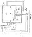
- FIG. 1is a schematic diagram of a prior art atomic layer deposition (ALD) apparatus
- FIG. 2is a schematic diagram of an atomic layer deposition (ALD) apparatus that can be used for the practice of embodiments described herein; and
- FIG. 3is a flow diagram of a process sequence for the atomic layer deposition (ALD) apparatus of FIG. 2 .
- FIG. 4is a schematic diagram of an atomic layer deposition (ALD) apparatus showing three potential deposition regions.
- ALDatomic layer deposition
- FIG. 2is perspective view of an atomic layer deposition (ALD) apparatus 100 that can be used to form a material layer on a semiconductor substrate in accordance with embodiments described herein.
- the ALD apparatus 100comprises a deposition chamber 105 , a gas panel 130 , a control unit 110 , along with other hardware components such as power supplies 106 and vacuum pumps 102 .
- the deposition chamber 105comprises two or more deposition regions 200 , 300 that are integrally connected to each other.
- the two or more deposition regions 200 , 300are configured as one above the other in a vertical arrangement, however it is contemplated that the two or more deposition regions may also be configured in a side by side horizontal arrangement (not shown).
- the two or more deposition regions 200 , 300are integrally connected one to another with an aperture 250 .
- the aperture 250is of a sufficient size to permit the passage therethrough of a wafer support 150 having a substrate thereon.
- the aperture 250is optionally sealed.
- the apertureis sealed to minimize the intermixing of deposition gases within the two or more deposition regions 200 , 300 . Physical and/or pressure differences may be used.
- an inert gas flowmay be used to minimize the intermixing of deposition gases at the aperture 250 between the two or more deposition regions 200 , 300 .
- the inert gas flowprovides a laminar flow around the area of the aperture 250 .
- the inert gas flowis provided around the area of the aperture 250 through orifices (not shown).
- the process chamber 105houses a wafer support 150 , which is used to support a substrate such as a semiconductor wafer 190 .
- the wafer support 150is moveable inside the chamber 105 between the integrally connected deposition regions 200 , 300 using a displacement mechanism (not shown).
- the semiconductor wafer 190can be heated to some desired temperature prior to material layer deposition.
- wafer support 150may be heated by an embedded heater element 170 .
- the wafer support 150may be resistively heated by applying an electric current from an AC power supply 106 to the heater element 170 .
- the wafer 190is, in turn, heated by the wafer support 190 .
- a temperature sensor 172such as a thermocouple, may also be embedded in the wafer support 150 to monitor the temperature of the support in a conventional manner. The measured temperature can be used in a feedback loop to control the power supplied to the heater element 170 , such that the wafer temperature can be maintained or controlled at a desired temperature which is suitable for the particular process application.
- the pedestalmay optionally be heated using radiant heat (not shown).
- a vacuum pump 102is used to evacuate each of the deposition regions 200 , 300 of the process chamber 105 and to maintain the proper gas flows and pressure inside the chamber 105 .
- Orifices 120provide process gases to each of the one or more deposition regions 200 , 300 .
- Each orifice 120is connected to a gas panel 130 via a gas line 125 , which controls and supplies various gases used in different steps of the deposition sequence.
- control unit 110Proper control and regulation of the gas flows through the gas panel 130 is performed by mass flow controllers (not shown) and the control unit 110 .
- the control unit 110comprises a central processing unit (CPU) 113 , as well as support circuitry 114 , and memories containing associated control software 116 .
- the control unit 110is responsible for automated control of the numerous steps required for wafer processing—such as movement of the wafer support, gas flow control, temperature control, chamber evacuation, and other steps.
- Bi-directional communications between the control unit 110 and the various components of the ALD 100are handled through numerous signal cables collectively referred to as signal buses 118 , some of which are illustrated in FIG. 2 .
- the central processing unit (CPU) 113may be one of any form of general purpose computer processor that can be used in an industrial setting for controlling process chambers as well as sub-processors.
- the computermay use any suitable memory, such as random access memory, read only memory, floppy disk drive, hard drive, or any other form of digital storage, local or remote.
- Various support circuitsmay be coupled to the CPU for supporting the processor in a conventional manner. Process sequence routines as required may be stored in the memory or executed by a second CPU that is remotely located.
- the process sequence routinesare executed after the substrate 190 is positioned on the wafer support 150 .
- the process sequence routineswhen executed, transform the general purpose computer into a specific process computer that controls the chamber operation so that the deposition process is performed.
- the chamber operationmay be controlled using remotely located hardware, as an application specific integrated circuit or other type of hardware implementation, or a combination of software and hardware.
- the ALD process sequencebegins when a semiconductor wafer is positioned on the wafer support in one of the two or more deposition regions 200 , 300 of the deposition chamber 105 , as indicated in step 350 .
- a deposition gasis provided to each of the two or more deposition regions 200 , 300 , as indicated in step 360 of FIG. 3 .
- a different deposition gasis provided to each of the two or more deposition regions 200 , 300 .
- the deposition gasesmay each be provided using a continuous flow, or optionally using a pulsed flow.
- alternating monolayers of each deposition gasare chemisorbed onto the surface of the semiconductor wafer to form a material layer having a desired thickness thereon.
- Each monolayeris chemisorbed onto the surface of the semiconductor wafer as the wafer support is alternately moved between the two or more deposition regions through aperture 250 .
Landscapes
- Chemical & Material Sciences (AREA)
- General Chemical & Material Sciences (AREA)
- Chemical Kinetics & Catalysis (AREA)
- Engineering & Computer Science (AREA)
- Materials Engineering (AREA)
- Mechanical Engineering (AREA)
- Metallurgy (AREA)
- Organic Chemistry (AREA)
- Chemical Vapour Deposition (AREA)
Abstract
Description
Claims (19)
Priority Applications (4)
| Application Number | Priority Date | Filing Date | Title |
|---|---|---|---|
| US12/646,706US7860597B2 (en) | 2001-07-27 | 2009-12-23 | Atomic layer deposition apparatus |
| US12/953,220US8027746B2 (en) | 2001-07-27 | 2010-11-23 | Atomic layer deposition apparatus |
| US13/235,855US8626330B2 (en) | 2001-07-27 | 2011-09-19 | Atomic layer deposition apparatus |
| US14/149,560US9031685B2 (en) | 2001-07-27 | 2014-01-07 | Atomic layer deposition apparatus |
Applications Claiming Priority (3)
| Application Number | Priority Date | Filing Date | Title |
|---|---|---|---|
| US09/917,842US7085616B2 (en) | 2001-07-27 | 2001-07-27 | Atomic layer deposition apparatus |
| US11/423,535US7660644B2 (en) | 2001-07-27 | 2006-06-12 | Atomic layer deposition apparatus |
| US12/646,706US7860597B2 (en) | 2001-07-27 | 2009-12-23 | Atomic layer deposition apparatus |
Related Parent Applications (1)
| Application Number | Title | Priority Date | Filing Date |
|---|---|---|---|
| US11/423,535ContinuationUS7660644B2 (en) | 2001-07-27 | 2006-06-12 | Atomic layer deposition apparatus |
Related Child Applications (1)
| Application Number | Title | Priority Date | Filing Date |
|---|---|---|---|
| US12/953,220ContinuationUS8027746B2 (en) | 2001-07-27 | 2010-11-23 | Atomic layer deposition apparatus |
Publications (2)
| Publication Number | Publication Date |
|---|---|
| US20100099270A1 US20100099270A1 (en) | 2010-04-22 |
| US7860597B2true US7860597B2 (en) | 2010-12-28 |
Family
ID=25439404
Family Applications (6)
| Application Number | Title | Priority Date | Filing Date |
|---|---|---|---|
| US09/917,842Expired - Fee RelatedUS7085616B2 (en) | 2001-07-27 | 2001-07-27 | Atomic layer deposition apparatus |
| US11/423,535Expired - Fee RelatedUS7660644B2 (en) | 2001-07-27 | 2006-06-12 | Atomic layer deposition apparatus |
| US12/646,706Expired - Fee RelatedUS7860597B2 (en) | 2001-07-27 | 2009-12-23 | Atomic layer deposition apparatus |
| US12/953,220Expired - Fee RelatedUS8027746B2 (en) | 2001-07-27 | 2010-11-23 | Atomic layer deposition apparatus |
| US13/235,855Expired - Fee RelatedUS8626330B2 (en) | 2001-07-27 | 2011-09-19 | Atomic layer deposition apparatus |
| US14/149,560Expired - Fee RelatedUS9031685B2 (en) | 2001-07-27 | 2014-01-07 | Atomic layer deposition apparatus |
Family Applications Before (2)
| Application Number | Title | Priority Date | Filing Date |
|---|---|---|---|
| US09/917,842Expired - Fee RelatedUS7085616B2 (en) | 2001-07-27 | 2001-07-27 | Atomic layer deposition apparatus |
| US11/423,535Expired - Fee RelatedUS7660644B2 (en) | 2001-07-27 | 2006-06-12 | Atomic layer deposition apparatus |
Family Applications After (3)
| Application Number | Title | Priority Date | Filing Date |
|---|---|---|---|
| US12/953,220Expired - Fee RelatedUS8027746B2 (en) | 2001-07-27 | 2010-11-23 | Atomic layer deposition apparatus |
| US13/235,855Expired - Fee RelatedUS8626330B2 (en) | 2001-07-27 | 2011-09-19 | Atomic layer deposition apparatus |
| US14/149,560Expired - Fee RelatedUS9031685B2 (en) | 2001-07-27 | 2014-01-07 | Atomic layer deposition apparatus |
Country Status (1)
| Country | Link |
|---|---|
| US (6) | US7085616B2 (en) |
Cited By (2)
| Publication number | Priority date | Publication date | Assignee | Title |
|---|---|---|---|---|
| US8027746B2 (en) | 2001-07-27 | 2011-09-27 | Applied Materials, Inc. | Atomic layer deposition apparatus |
| US20110305836A1 (en)* | 2009-03-10 | 2011-12-15 | Mitsui Engineering & Shipbuilding Co., Ltd. | Atomic layer deposition apparatus and thin film forming method |
Families Citing this family (426)
| Publication number | Priority date | Publication date | Assignee | Title |
|---|---|---|---|---|
| US6951804B2 (en)* | 2001-02-02 | 2005-10-04 | Applied Materials, Inc. | Formation of a tantalum-nitride layer |
| US6878206B2 (en) | 2001-07-16 | 2005-04-12 | Applied Materials, Inc. | Lid assembly for a processing system to facilitate sequential deposition techniques |
| US6718126B2 (en)* | 2001-09-14 | 2004-04-06 | Applied Materials, Inc. | Apparatus and method for vaporizing solid precursor for CVD or atomic layer deposition |
| US7049226B2 (en) | 2001-09-26 | 2006-05-23 | Applied Materials, Inc. | Integration of ALD tantalum nitride for copper metallization |
| US6936906B2 (en) | 2001-09-26 | 2005-08-30 | Applied Materials, Inc. | Integration of barrier layer and seed layer |
| US6916398B2 (en)* | 2001-10-26 | 2005-07-12 | Applied Materials, Inc. | Gas delivery apparatus and method for atomic layer deposition |
| US7780785B2 (en) | 2001-10-26 | 2010-08-24 | Applied Materials, Inc. | Gas delivery apparatus for atomic layer deposition |
| US6670071B2 (en)* | 2002-01-15 | 2003-12-30 | Quallion Llc | Electric storage battery construction and method of manufacture |
| AU2003238853A1 (en)* | 2002-01-25 | 2003-09-02 | Applied Materials, Inc. | Apparatus for cyclical deposition of thin films |
| US6911391B2 (en) | 2002-01-26 | 2005-06-28 | Applied Materials, Inc. | Integration of titanium and titanium nitride layers |
| US6972267B2 (en) | 2002-03-04 | 2005-12-06 | Applied Materials, Inc. | Sequential deposition of tantalum nitride using a tantalum-containing precursor and a nitrogen-containing precursor |
| US6861094B2 (en)* | 2002-04-25 | 2005-03-01 | Micron Technology, Inc. | Methods for forming thin layers of materials on micro-device workpieces |
| WO2003100816A2 (en)* | 2002-05-20 | 2003-12-04 | The University Of Houston System | Energetic neutral particle lithographic apparatus and process |
| US6838114B2 (en)* | 2002-05-24 | 2005-01-04 | Micron Technology, Inc. | Methods for controlling gas pulsing in processes for depositing materials onto micro-device workpieces |
| US7118783B2 (en)* | 2002-06-26 | 2006-10-10 | Micron Technology, Inc. | Methods and apparatus for vapor processing of micro-device workpieces |
| US6821347B2 (en)* | 2002-07-08 | 2004-11-23 | Micron Technology, Inc. | Apparatus and method for depositing materials onto microelectronic workpieces |
| US7186385B2 (en) | 2002-07-17 | 2007-03-06 | Applied Materials, Inc. | Apparatus for providing gas to a processing chamber |
| US6955725B2 (en) | 2002-08-15 | 2005-10-18 | Micron Technology, Inc. | Reactors with isolated gas connectors and methods for depositing materials onto micro-device workpieces |
| AU2003258237A1 (en)* | 2002-08-26 | 2004-03-11 | Tokyo Electron Limited | Reduced volume plasma reactor |
| EP1420080A3 (en) | 2002-11-14 | 2005-11-09 | Applied Materials, Inc. | Apparatus and method for hybrid chemical deposition processes |
| US6972055B2 (en)* | 2003-03-28 | 2005-12-06 | Finens Corporation | Continuous flow deposition system |
| US7335396B2 (en)* | 2003-04-24 | 2008-02-26 | Micron Technology, Inc. | Methods for controlling mass flow rates and pressures in passageways coupled to reaction chambers and systems for depositing material onto microfeature workpieces in reaction chambers |
| US6921437B1 (en)* | 2003-05-30 | 2005-07-26 | Aviza Technology, Inc. | Gas distribution system |
| US7344755B2 (en)* | 2003-08-21 | 2008-03-18 | Micron Technology, Inc. | Methods and apparatus for processing microfeature workpieces; methods for conditioning ALD reaction chambers |
| US7235138B2 (en) | 2003-08-21 | 2007-06-26 | Micron Technology, Inc. | Microfeature workpiece processing apparatus and methods for batch deposition of materials on microfeature workpieces |
| US8346482B2 (en)* | 2003-08-22 | 2013-01-01 | Fernandez Dennis S | Integrated biosensor and simulation system for diagnosis and therapy |
| US7422635B2 (en)* | 2003-08-28 | 2008-09-09 | Micron Technology, Inc. | Methods and apparatus for processing microfeature workpieces, e.g., for depositing materials on microfeature workpieces |
| US7056806B2 (en) | 2003-09-17 | 2006-06-06 | Micron Technology, Inc. | Microfeature workpiece processing apparatus and methods for controlling deposition of materials on microfeature workpieces |
| US7282239B2 (en)* | 2003-09-18 | 2007-10-16 | Micron Technology, Inc. | Systems and methods for depositing material onto microfeature workpieces in reaction chambers |
| US7323231B2 (en)* | 2003-10-09 | 2008-01-29 | Micron Technology, Inc. | Apparatus and methods for plasma vapor deposition processes |
| US7581511B2 (en)* | 2003-10-10 | 2009-09-01 | Micron Technology, Inc. | Apparatus and methods for manufacturing microfeatures on workpieces using plasma vapor processes |
| US7647886B2 (en)* | 2003-10-15 | 2010-01-19 | Micron Technology, Inc. | Systems for depositing material onto workpieces in reaction chambers and methods for removing byproducts from reaction chambers |
| US20050095859A1 (en)* | 2003-11-03 | 2005-05-05 | Applied Materials, Inc. | Precursor delivery system with rate control |
| US7258892B2 (en)* | 2003-12-10 | 2007-08-21 | Micron Technology, Inc. | Methods and systems for controlling temperature during microfeature workpiece processing, e.g., CVD deposition |
| US7906393B2 (en) | 2004-01-28 | 2011-03-15 | Micron Technology, Inc. | Methods for forming small-scale capacitor structures |
| US7584942B2 (en) | 2004-03-31 | 2009-09-08 | Micron Technology, Inc. | Ampoules for producing a reaction gas and systems for depositing materials onto microfeature workpieces in reaction chambers |
| US7700155B1 (en)* | 2004-04-08 | 2010-04-20 | Novellus Systems, Inc. | Method and apparatus for modulation of precursor exposure during a pulsed deposition process |
| US20050249873A1 (en)* | 2004-05-05 | 2005-11-10 | Demetrius Sarigiannis | Apparatuses and methods for producing chemically reactive vapors used in manufacturing microelectronic devices |
| US8133554B2 (en) | 2004-05-06 | 2012-03-13 | Micron Technology, Inc. | Methods for depositing material onto microfeature workpieces in reaction chambers and systems for depositing materials onto microfeature workpieces |
| US20050252449A1 (en) | 2004-05-12 | 2005-11-17 | Nguyen Son T | Control of gas flow and delivery to suppress the formation of particles in an MOCVD/ALD system |
| US7699932B2 (en)* | 2004-06-02 | 2010-04-20 | Micron Technology, Inc. | Reactors, systems and methods for depositing thin films onto microfeature workpieces |
| JP2006176826A (en)* | 2004-12-22 | 2006-07-06 | Canon Anelva Corp | Thin film processing equipment |
| US20060165873A1 (en)* | 2005-01-25 | 2006-07-27 | Micron Technology, Inc. | Plasma detection and associated systems and methods for controlling microfeature workpiece deposition processes |
| US20060237138A1 (en)* | 2005-04-26 | 2006-10-26 | Micron Technology, Inc. | Apparatuses and methods for supporting microelectronic devices during plasma-based fabrication processes |
| KR20080033406A (en)* | 2005-07-29 | 2008-04-16 | 에비자 테크놀로지, 인크. | Deposition apparatus for semiconductor processing |
| TWI332532B (en) | 2005-11-04 | 2010-11-01 | Applied Materials Inc | Apparatus and process for plasma-enhanced atomic layer deposition |
| WO2007075435A2 (en)* | 2005-12-15 | 2007-07-05 | Fluens Corporation | Apparatus for reactive sputtering |
| US8226769B2 (en) | 2006-04-27 | 2012-07-24 | Applied Materials, Inc. | Substrate support with electrostatic chuck having dual temperature zones |
| US7798096B2 (en) | 2006-05-05 | 2010-09-21 | Applied Materials, Inc. | Plasma, UV and ion/neutral assisted ALD or CVD in a batch tool |
| US9275887B2 (en) | 2006-07-20 | 2016-03-01 | Applied Materials, Inc. | Substrate processing with rapid temperature gradient control |
| US7775508B2 (en)* | 2006-10-31 | 2010-08-17 | Applied Materials, Inc. | Ampoule for liquid draw and vapor draw with a continuous level sensor |
| US8821637B2 (en)* | 2007-01-29 | 2014-09-02 | Applied Materials, Inc. | Temperature controlled lid assembly for tungsten nitride deposition |
| JP5022116B2 (en)* | 2007-06-18 | 2012-09-12 | 三菱重工業株式会社 | Semiconductor device manufacturing method and manufacturing apparatus |
| US7769891B2 (en) | 2007-08-27 | 2010-08-03 | International Business Machines Corporation | System and method for providing multiple redundant direct routes between supernodes of a multi-tiered full-graph interconnect architecture |
| KR100949914B1 (en)* | 2007-11-28 | 2010-03-30 | 주식회사 케이씨텍 | Atomic layer deposition apparatus |
| JP2010073822A (en)* | 2008-09-17 | 2010-04-02 | Tokyo Electron Ltd | Film deposition apparatus, film deposition method, program and computer readable storage medium |
| US20100075488A1 (en)* | 2008-09-19 | 2010-03-25 | Applied Materials, Inc. | Cvd reactor with multiple processing levels and dual-axis motorized lift mechanism |
| US8146896B2 (en)* | 2008-10-31 | 2012-04-03 | Applied Materials, Inc. | Chemical precursor ampoule for vapor deposition processes |
| US10378106B2 (en) | 2008-11-14 | 2019-08-13 | Asm Ip Holding B.V. | Method of forming insulation film by modified PEALD |
| US20100183825A1 (en)* | 2008-12-31 | 2010-07-22 | Cambridge Nanotech Inc. | Plasma atomic layer deposition system and method |
| US20100221426A1 (en)* | 2009-03-02 | 2010-09-02 | Fluens Corporation | Web Substrate Deposition System |
| US9394608B2 (en) | 2009-04-06 | 2016-07-19 | Asm America, Inc. | Semiconductor processing reactor and components thereof |
| US8802201B2 (en) | 2009-08-14 | 2014-08-12 | Asm America, Inc. | Systems and methods for thin-film deposition of metal oxides using excited nitrogen-oxygen species |
| US20110120544A1 (en) | 2009-11-20 | 2011-05-26 | Levy David H | Deposition inhibitor composition and method of use |
| WO2011062779A1 (en) | 2009-11-20 | 2011-05-26 | Eastman Kodak Company | Method for selective deposition and devices |
| US9512520B2 (en)* | 2011-04-25 | 2016-12-06 | Applied Materials, Inc. | Semiconductor substrate processing system |
| US9312155B2 (en) | 2011-06-06 | 2016-04-12 | Asm Japan K.K. | High-throughput semiconductor-processing apparatus equipped with multiple dual-chamber modules |
| US10364496B2 (en) | 2011-06-27 | 2019-07-30 | Asm Ip Holding B.V. | Dual section module having shared and unshared mass flow controllers |
| US10854498B2 (en) | 2011-07-15 | 2020-12-01 | Asm Ip Holding B.V. | Wafer-supporting device and method for producing same |
| US20130023129A1 (en) | 2011-07-20 | 2013-01-24 | Asm America, Inc. | Pressure transmitter for a semiconductor processing environment |
| US9017481B1 (en) | 2011-10-28 | 2015-04-28 | Asm America, Inc. | Process feed management for semiconductor substrate processing |
| US8618003B2 (en) | 2011-12-05 | 2013-12-31 | Eastman Kodak Company | Method of making electronic devices using selective deposition |
| US9659799B2 (en) | 2012-08-28 | 2017-05-23 | Asm Ip Holding B.V. | Systems and methods for dynamic semiconductor process scheduling |
| US10714315B2 (en) | 2012-10-12 | 2020-07-14 | Asm Ip Holdings B.V. | Semiconductor reaction chamber showerhead |
| US20160376700A1 (en) | 2013-02-01 | 2016-12-29 | Asm Ip Holding B.V. | System for treatment of deposition reactor |
| US9484191B2 (en) | 2013-03-08 | 2016-11-01 | Asm Ip Holding B.V. | Pulsed remote plasma method and system |
| US9589770B2 (en) | 2013-03-08 | 2017-03-07 | Asm Ip Holding B.V. | Method and systems for in-situ formation of intermediate reactive species |
| US9353439B2 (en) | 2013-04-05 | 2016-05-31 | Lam Research Corporation | Cascade design showerhead for transient uniformity |
| JP6411484B2 (en)* | 2013-06-27 | 2018-10-24 | ピコサン オーワイPicosun Oy | Anti-counterfeit signature |
| US9240412B2 (en) | 2013-09-27 | 2016-01-19 | Asm Ip Holding B.V. | Semiconductor structure and device and methods of forming same using selective epitaxial process |
| KR102173047B1 (en)* | 2013-10-10 | 2020-11-03 | 삼성디스플레이 주식회사 | Vapor deposition apparatus |
| CN103602959B (en)* | 2013-11-19 | 2016-04-13 | 华中科技大学 | A kind of Atomic layer deposition precursor body output device |
| US10683571B2 (en) | 2014-02-25 | 2020-06-16 | Asm Ip Holding B.V. | Gas supply manifold and method of supplying gases to chamber using same |
| US10167557B2 (en) | 2014-03-18 | 2019-01-01 | Asm Ip Holding B.V. | Gas distribution system, reactor including the system, and methods of using the same |
| US11015245B2 (en) | 2014-03-19 | 2021-05-25 | Asm Ip Holding B.V. | Gas-phase reactor and system having exhaust plenum and components thereof |
| US10858737B2 (en) | 2014-07-28 | 2020-12-08 | Asm Ip Holding B.V. | Showerhead assembly and components thereof |
| US9890456B2 (en) | 2014-08-21 | 2018-02-13 | Asm Ip Holding B.V. | Method and system for in situ formation of gas-phase compounds |
| US10941490B2 (en) | 2014-10-07 | 2021-03-09 | Asm Ip Holding B.V. | Multiple temperature range susceptor, assembly, reactor and system including the susceptor, and methods of using the same |
| US9657845B2 (en) | 2014-10-07 | 2017-05-23 | Asm Ip Holding B.V. | Variable conductance gas distribution apparatus and method |
| JP6062413B2 (en)* | 2014-11-28 | 2017-01-18 | 株式会社日立国際電気 | Substrate processing apparatus, semiconductor device manufacturing method, and program |
| KR102263121B1 (en) | 2014-12-22 | 2021-06-09 | 에이에스엠 아이피 홀딩 비.브이. | Semiconductor device and manufacuring method thereof |
| US10529542B2 (en) | 2015-03-11 | 2020-01-07 | Asm Ip Holdings B.V. | Cross-flow reactor and method |
| US10276355B2 (en)* | 2015-03-12 | 2019-04-30 | Asm Ip Holding B.V. | Multi-zone reactor, system including the reactor, and method of using the same |
| US10023959B2 (en) | 2015-05-26 | 2018-07-17 | Lam Research Corporation | Anti-transient showerhead |
| US10458018B2 (en) | 2015-06-26 | 2019-10-29 | Asm Ip Holding B.V. | Structures including metal carbide material, devices including the structures, and methods of forming same |
| US10600673B2 (en) | 2015-07-07 | 2020-03-24 | Asm Ip Holding B.V. | Magnetic susceptor to baseplate seal |
| US10083836B2 (en) | 2015-07-24 | 2018-09-25 | Asm Ip Holding B.V. | Formation of boron-doped titanium metal films with high work function |
| US9960072B2 (en) | 2015-09-29 | 2018-05-01 | Asm Ip Holding B.V. | Variable adjustment for precise matching of multiple chamber cavity housings |
| US10211308B2 (en) | 2015-10-21 | 2019-02-19 | Asm Ip Holding B.V. | NbMC layers |
| US10322384B2 (en) | 2015-11-09 | 2019-06-18 | Asm Ip Holding B.V. | Counter flow mixer for process chamber |
| US11139308B2 (en) | 2015-12-29 | 2021-10-05 | Asm Ip Holding B.V. | Atomic layer deposition of III-V compounds to form V-NAND devices |
| US20170207078A1 (en)* | 2016-01-15 | 2017-07-20 | Taiwan Semiconductor Manufacturing Co., Ltd. | Atomic layer deposition apparatus and semiconductor process |
| US9953843B2 (en) | 2016-02-05 | 2018-04-24 | Lam Research Corporation | Chamber for patterning non-volatile metals |
| US10468251B2 (en) | 2016-02-19 | 2019-11-05 | Asm Ip Holding B.V. | Method for forming spacers using silicon nitride film for spacer-defined multiple patterning |
| US10529554B2 (en) | 2016-02-19 | 2020-01-07 | Asm Ip Holding B.V. | Method for forming silicon nitride film selectively on sidewalls or flat surfaces of trenches |
| US10501866B2 (en) | 2016-03-09 | 2019-12-10 | Asm Ip Holding B.V. | Gas distribution apparatus for improved film uniformity in an epitaxial system |
| US10343920B2 (en) | 2016-03-18 | 2019-07-09 | Asm Ip Holding B.V. | Aligned carbon nanotubes |
| US9892913B2 (en) | 2016-03-24 | 2018-02-13 | Asm Ip Holding B.V. | Radial and thickness control via biased multi-port injection settings |
| US10190213B2 (en) | 2016-04-21 | 2019-01-29 | Asm Ip Holding B.V. | Deposition of metal borides |
| US10865475B2 (en) | 2016-04-21 | 2020-12-15 | Asm Ip Holding B.V. | Deposition of metal borides and silicides |
| US10367080B2 (en) | 2016-05-02 | 2019-07-30 | Asm Ip Holding B.V. | Method of forming a germanium oxynitride film |
| US10032628B2 (en) | 2016-05-02 | 2018-07-24 | Asm Ip Holding B.V. | Source/drain performance through conformal solid state doping |
| KR102592471B1 (en) | 2016-05-17 | 2023-10-20 | 에이에스엠 아이피 홀딩 비.브이. | Method of forming metal interconnection and method of fabricating semiconductor device using the same |
| US11453943B2 (en) | 2016-05-25 | 2022-09-27 | Asm Ip Holding B.V. | Method for forming carbon-containing silicon/metal oxide or nitride film by ALD using silicon precursor and hydrocarbon precursor |
| US10388509B2 (en) | 2016-06-28 | 2019-08-20 | Asm Ip Holding B.V. | Formation of epitaxial layers via dislocation filtering |
| US9859151B1 (en) | 2016-07-08 | 2018-01-02 | Asm Ip Holding B.V. | Selective film deposition method to form air gaps |
| US10612137B2 (en) | 2016-07-08 | 2020-04-07 | Asm Ip Holdings B.V. | Organic reactants for atomic layer deposition |
| US10714385B2 (en) | 2016-07-19 | 2020-07-14 | Asm Ip Holding B.V. | Selective deposition of tungsten |
| KR102354490B1 (en) | 2016-07-27 | 2022-01-21 | 에이에스엠 아이피 홀딩 비.브이. | Method of processing a substrate |
| US9812320B1 (en) | 2016-07-28 | 2017-11-07 | Asm Ip Holding B.V. | Method and apparatus for filling a gap |
| US10395919B2 (en) | 2016-07-28 | 2019-08-27 | Asm Ip Holding B.V. | Method and apparatus for filling a gap |
| KR102532607B1 (en) | 2016-07-28 | 2023-05-15 | 에이에스엠 아이피 홀딩 비.브이. | Substrate processing apparatus and method of operating the same |
| US9887082B1 (en) | 2016-07-28 | 2018-02-06 | Asm Ip Holding B.V. | Method and apparatus for filling a gap |
| JP6446418B2 (en)* | 2016-09-13 | 2018-12-26 | 株式会社Kokusai Electric | Semiconductor device manufacturing method, substrate processing apparatus, and program |
| US10410943B2 (en) | 2016-10-13 | 2019-09-10 | Asm Ip Holding B.V. | Method for passivating a surface of a semiconductor and related systems |
| US10643826B2 (en) | 2016-10-26 | 2020-05-05 | Asm Ip Holdings B.V. | Methods for thermally calibrating reaction chambers |
| US11532757B2 (en) | 2016-10-27 | 2022-12-20 | Asm Ip Holding B.V. | Deposition of charge trapping layers |
| US10229833B2 (en) | 2016-11-01 | 2019-03-12 | Asm Ip Holding B.V. | Methods for forming a transition metal nitride film on a substrate by atomic layer deposition and related semiconductor device structures |
| US10643904B2 (en) | 2016-11-01 | 2020-05-05 | Asm Ip Holdings B.V. | Methods for forming a semiconductor device and related semiconductor device structures |
| US10714350B2 (en) | 2016-11-01 | 2020-07-14 | ASM IP Holdings, B.V. | Methods for forming a transition metal niobium nitride film on a substrate by atomic layer deposition and related semiconductor device structures |
| US10435790B2 (en) | 2016-11-01 | 2019-10-08 | Asm Ip Holding B.V. | Method of subatmospheric plasma-enhanced ALD using capacitively coupled electrodes with narrow gap |
| US10134757B2 (en) | 2016-11-07 | 2018-11-20 | Asm Ip Holding B.V. | Method of processing a substrate and a device manufactured by using the method |
| KR102546317B1 (en) | 2016-11-15 | 2023-06-21 | 에이에스엠 아이피 홀딩 비.브이. | Gas supply unit and substrate processing apparatus including the same |
| US10340135B2 (en) | 2016-11-28 | 2019-07-02 | Asm Ip Holding B.V. | Method of topologically restricted plasma-enhanced cyclic deposition of silicon or metal nitride |
| KR102762543B1 (en) | 2016-12-14 | 2025-02-05 | 에이에스엠 아이피 홀딩 비.브이. | Substrate processing apparatus |
| US11581186B2 (en) | 2016-12-15 | 2023-02-14 | Asm Ip Holding B.V. | Sequential infiltration synthesis apparatus |
| US11447861B2 (en) | 2016-12-15 | 2022-09-20 | Asm Ip Holding B.V. | Sequential infiltration synthesis apparatus and a method of forming a patterned structure |
| KR102700194B1 (en) | 2016-12-19 | 2024-08-28 | 에이에스엠 아이피 홀딩 비.브이. | Substrate processing apparatus |
| US10269558B2 (en) | 2016-12-22 | 2019-04-23 | Asm Ip Holding B.V. | Method of forming a structure on a substrate |
| US10867788B2 (en) | 2016-12-28 | 2020-12-15 | Asm Ip Holding B.V. | Method of forming a structure on a substrate |
| US11390950B2 (en) | 2017-01-10 | 2022-07-19 | Asm Ip Holding B.V. | Reactor system and method to reduce residue buildup during a film deposition process |
| US10655221B2 (en) | 2017-02-09 | 2020-05-19 | Asm Ip Holding B.V. | Method for depositing oxide film by thermal ALD and PEALD |
| US10468261B2 (en) | 2017-02-15 | 2019-11-05 | Asm Ip Holding B.V. | Methods for forming a metallic film on a substrate by cyclical deposition and related semiconductor device structures |
| US10529563B2 (en) | 2017-03-29 | 2020-01-07 | Asm Ip Holdings B.V. | Method for forming doped metal oxide films on a substrate by cyclical deposition and related semiconductor device structures |
| US10283353B2 (en) | 2017-03-29 | 2019-05-07 | Asm Ip Holding B.V. | Method of reforming insulating film deposited on substrate with recess pattern |
| KR102457289B1 (en) | 2017-04-25 | 2022-10-21 | 에이에스엠 아이피 홀딩 비.브이. | Method for depositing a thin film and manufacturing a semiconductor device |
| US10446393B2 (en) | 2017-05-08 | 2019-10-15 | Asm Ip Holding B.V. | Methods for forming silicon-containing epitaxial layers and related semiconductor device structures |
| US10770286B2 (en) | 2017-05-08 | 2020-09-08 | Asm Ip Holdings B.V. | Methods for selectively forming a silicon nitride film on a substrate and related semiconductor device structures |
| US10892156B2 (en) | 2017-05-08 | 2021-01-12 | Asm Ip Holding B.V. | Methods for forming a silicon nitride film on a substrate and related semiconductor device structures |
| US10504742B2 (en) | 2017-05-31 | 2019-12-10 | Asm Ip Holding B.V. | Method of atomic layer etching using hydrogen plasma |
| US10886123B2 (en) | 2017-06-02 | 2021-01-05 | Asm Ip Holding B.V. | Methods for forming low temperature semiconductor layers and related semiconductor device structures |
| US12040200B2 (en) | 2017-06-20 | 2024-07-16 | Asm Ip Holding B.V. | Semiconductor processing apparatus and methods for calibrating a semiconductor processing apparatus |
| US11306395B2 (en) | 2017-06-28 | 2022-04-19 | Asm Ip Holding B.V. | Methods for depositing a transition metal nitride film on a substrate by atomic layer deposition and related deposition apparatus |
| US10685834B2 (en) | 2017-07-05 | 2020-06-16 | Asm Ip Holdings B.V. | Methods for forming a silicon germanium tin layer and related semiconductor device structures |
| KR20190009245A (en) | 2017-07-18 | 2019-01-28 | 에이에스엠 아이피 홀딩 비.브이. | Methods for forming a semiconductor device structure and related semiconductor device structures |
| US10541333B2 (en) | 2017-07-19 | 2020-01-21 | Asm Ip Holding B.V. | Method for depositing a group IV semiconductor and related semiconductor device structures |
| US11374112B2 (en) | 2017-07-19 | 2022-06-28 | Asm Ip Holding B.V. | Method for depositing a group IV semiconductor and related semiconductor device structures |
| US11018002B2 (en) | 2017-07-19 | 2021-05-25 | Asm Ip Holding B.V. | Method for selectively depositing a Group IV semiconductor and related semiconductor device structures |
| US10312055B2 (en) | 2017-07-26 | 2019-06-04 | Asm Ip Holding B.V. | Method of depositing film by PEALD using negative bias |
| US10590535B2 (en) | 2017-07-26 | 2020-03-17 | Asm Ip Holdings B.V. | Chemical treatment, deposition and/or infiltration apparatus and method for using the same |
| US10605530B2 (en) | 2017-07-26 | 2020-03-31 | Asm Ip Holding B.V. | Assembly of a liner and a flange for a vertical furnace as well as the liner and the vertical furnace |
| TWI815813B (en) | 2017-08-04 | 2023-09-21 | 荷蘭商Asm智慧財產控股公司 | Showerhead assembly for distributing a gas within a reaction chamber |
| US10692741B2 (en) | 2017-08-08 | 2020-06-23 | Asm Ip Holdings B.V. | Radiation shield |
| US10770336B2 (en) | 2017-08-08 | 2020-09-08 | Asm Ip Holding B.V. | Substrate lift mechanism and reactor including same |
| US11139191B2 (en) | 2017-08-09 | 2021-10-05 | Asm Ip Holding B.V. | Storage apparatus for storing cassettes for substrates and processing apparatus equipped therewith |
| US11769682B2 (en) | 2017-08-09 | 2023-09-26 | Asm Ip Holding B.V. | Storage apparatus for storing cassettes for substrates and processing apparatus equipped therewith |
| US10249524B2 (en) | 2017-08-09 | 2019-04-02 | Asm Ip Holding B.V. | Cassette holder assembly for a substrate cassette and holding member for use in such assembly |
| USD900036S1 (en) | 2017-08-24 | 2020-10-27 | Asm Ip Holding B.V. | Heater electrical connector and adapter |
| US11830730B2 (en) | 2017-08-29 | 2023-11-28 | Asm Ip Holding B.V. | Layer forming method and apparatus |
| US11295980B2 (en) | 2017-08-30 | 2022-04-05 | Asm Ip Holding B.V. | Methods for depositing a molybdenum metal film over a dielectric surface of a substrate by a cyclical deposition process and related semiconductor device structures |
| KR102491945B1 (en) | 2017-08-30 | 2023-01-26 | 에이에스엠 아이피 홀딩 비.브이. | Substrate processing apparatus |
| US11056344B2 (en) | 2017-08-30 | 2021-07-06 | Asm Ip Holding B.V. | Layer forming method |
| KR102401446B1 (en) | 2017-08-31 | 2022-05-24 | 에이에스엠 아이피 홀딩 비.브이. | Substrate processing apparatus |
| CN107680576A (en)* | 2017-09-07 | 2018-02-09 | 国家电网公司 | Active Frequency Point Follower Phononic Crystal and Its Noise Reduction Method |
| US10607895B2 (en) | 2017-09-18 | 2020-03-31 | Asm Ip Holdings B.V. | Method for forming a semiconductor device structure comprising a gate fill metal |
| KR102630301B1 (en) | 2017-09-21 | 2024-01-29 | 에이에스엠 아이피 홀딩 비.브이. | Method of sequential infiltration synthesis treatment of infiltrateable material and structures and devices formed using same |
| US10844484B2 (en) | 2017-09-22 | 2020-11-24 | Asm Ip Holding B.V. | Apparatus for dispensing a vapor phase reactant to a reaction chamber and related methods |
| US10658205B2 (en) | 2017-09-28 | 2020-05-19 | Asm Ip Holdings B.V. | Chemical dispensing apparatus and methods for dispensing a chemical to a reaction chamber |
| US10403504B2 (en) | 2017-10-05 | 2019-09-03 | Asm Ip Holding B.V. | Method for selectively depositing a metallic film on a substrate |
| US10319588B2 (en) | 2017-10-10 | 2019-06-11 | Asm Ip Holding B.V. | Method for depositing a metal chalcogenide on a substrate by cyclical deposition |
| US10923344B2 (en) | 2017-10-30 | 2021-02-16 | Asm Ip Holding B.V. | Methods for forming a semiconductor structure and related semiconductor structures |
| US10910262B2 (en) | 2017-11-16 | 2021-02-02 | Asm Ip Holding B.V. | Method of selectively depositing a capping layer structure on a semiconductor device structure |
| KR102443047B1 (en) | 2017-11-16 | 2022-09-14 | 에이에스엠 아이피 홀딩 비.브이. | Method of processing a substrate and a device manufactured by the same |
| KR102300756B1 (en) | 2017-11-21 | 2021-09-10 | 와틀로 일렉트릭 매뉴팩츄어링 컴파니 | Ceramic pedestal with atomic protective layer |
| US11022879B2 (en) | 2017-11-24 | 2021-06-01 | Asm Ip Holding B.V. | Method of forming an enhanced unexposed photoresist layer |
| WO2019103613A1 (en) | 2017-11-27 | 2019-05-31 | Asm Ip Holding B.V. | A storage device for storing wafer cassettes for use with a batch furnace |
| CN111344522B (en) | 2017-11-27 | 2022-04-12 | 阿斯莫Ip控股公司 | Including clean mini-environment device |
| US10290508B1 (en) | 2017-12-05 | 2019-05-14 | Asm Ip Holding B.V. | Method for forming vertical spacers for spacer-defined patterning |
| US10872771B2 (en) | 2018-01-16 | 2020-12-22 | Asm Ip Holding B. V. | Method for depositing a material film on a substrate within a reaction chamber by a cyclical deposition process and related device structures |
| TWI799494B (en) | 2018-01-19 | 2023-04-21 | 荷蘭商Asm 智慧財產控股公司 | Deposition method |
| KR102695659B1 (en) | 2018-01-19 | 2024-08-14 | 에이에스엠 아이피 홀딩 비.브이. | Method for depositing a gap filling layer by plasma assisted deposition |
| USD903477S1 (en) | 2018-01-24 | 2020-12-01 | Asm Ip Holdings B.V. | Metal clamp |
| US11018047B2 (en) | 2018-01-25 | 2021-05-25 | Asm Ip Holding B.V. | Hybrid lift pin |
| USD880437S1 (en) | 2018-02-01 | 2020-04-07 | Asm Ip Holding B.V. | Gas supply plate for semiconductor manufacturing apparatus |
| US10535516B2 (en) | 2018-02-01 | 2020-01-14 | Asm Ip Holdings B.V. | Method for depositing a semiconductor structure on a surface of a substrate and related semiconductor structures |
| US11081345B2 (en) | 2018-02-06 | 2021-08-03 | Asm Ip Holding B.V. | Method of post-deposition treatment for silicon oxide film |
| WO2019158960A1 (en) | 2018-02-14 | 2019-08-22 | Asm Ip Holding B.V. | A method for depositing a ruthenium-containing film on a substrate by a cyclical deposition process |
| US10896820B2 (en) | 2018-02-14 | 2021-01-19 | Asm Ip Holding B.V. | Method for depositing a ruthenium-containing film on a substrate by a cyclical deposition process |
| US10731249B2 (en) | 2018-02-15 | 2020-08-04 | Asm Ip Holding B.V. | Method of forming a transition metal containing film on a substrate by a cyclical deposition process, a method for supplying a transition metal halide compound to a reaction chamber, and related vapor deposition apparatus |
| US10658181B2 (en) | 2018-02-20 | 2020-05-19 | Asm Ip Holding B.V. | Method of spacer-defined direct patterning in semiconductor fabrication |
| KR102636427B1 (en) | 2018-02-20 | 2024-02-13 | 에이에스엠 아이피 홀딩 비.브이. | Substrate processing method and apparatus |
| US10975470B2 (en) | 2018-02-23 | 2021-04-13 | Asm Ip Holding B.V. | Apparatus for detecting or monitoring for a chemical precursor in a high temperature environment |
| US11473195B2 (en) | 2018-03-01 | 2022-10-18 | Asm Ip Holding B.V. | Semiconductor processing apparatus and a method for processing a substrate |
| US11629406B2 (en) | 2018-03-09 | 2023-04-18 | Asm Ip Holding B.V. | Semiconductor processing apparatus comprising one or more pyrometers for measuring a temperature of a substrate during transfer of the substrate |
| US11114283B2 (en) | 2018-03-16 | 2021-09-07 | Asm Ip Holding B.V. | Reactor, system including the reactor, and methods of manufacturing and using same |
| KR102646467B1 (en) | 2018-03-27 | 2024-03-11 | 에이에스엠 아이피 홀딩 비.브이. | Method of forming an electrode on a substrate and a semiconductor device structure including an electrode |
| US10510536B2 (en) | 2018-03-29 | 2019-12-17 | Asm Ip Holding B.V. | Method of depositing a co-doped polysilicon film on a surface of a substrate within a reaction chamber |
| US11230766B2 (en) | 2018-03-29 | 2022-01-25 | Asm Ip Holding B.V. | Substrate processing apparatus and method |
| US11088002B2 (en) | 2018-03-29 | 2021-08-10 | Asm Ip Holding B.V. | Substrate rack and a substrate processing system and method |
| KR102501472B1 (en) | 2018-03-30 | 2023-02-20 | 에이에스엠 아이피 홀딩 비.브이. | Substrate processing method |
| KR102600229B1 (en) | 2018-04-09 | 2023-11-10 | 에이에스엠 아이피 홀딩 비.브이. | Substrate supporting device, substrate processing apparatus including the same and substrate processing method |
| TWI811348B (en) | 2018-05-08 | 2023-08-11 | 荷蘭商Asm 智慧財產控股公司 | Methods for depositing an oxide film on a substrate by a cyclical deposition process and related device structures |
| US12025484B2 (en) | 2018-05-08 | 2024-07-02 | Asm Ip Holding B.V. | Thin film forming method |
| US12272527B2 (en) | 2018-05-09 | 2025-04-08 | Asm Ip Holding B.V. | Apparatus for use with hydrogen radicals and method of using same |
| KR20190129718A (en) | 2018-05-11 | 2019-11-20 | 에이에스엠 아이피 홀딩 비.브이. | Methods for forming a doped metal carbide film on a substrate and related semiconductor device structures |
| KR102596988B1 (en) | 2018-05-28 | 2023-10-31 | 에이에스엠 아이피 홀딩 비.브이. | Method of processing a substrate and a device manufactured by the same |
| US11718913B2 (en) | 2018-06-04 | 2023-08-08 | Asm Ip Holding B.V. | Gas distribution system and reactor system including same |
| TWI840362B (en) | 2018-06-04 | 2024-05-01 | 荷蘭商Asm Ip私人控股有限公司 | Wafer handling chamber with moisture reduction |
| US11286562B2 (en) | 2018-06-08 | 2022-03-29 | Asm Ip Holding B.V. | Gas-phase chemical reactor and method of using same |
| KR102568797B1 (en) | 2018-06-21 | 2023-08-21 | 에이에스엠 아이피 홀딩 비.브이. | Substrate processing system |
| US10797133B2 (en) | 2018-06-21 | 2020-10-06 | Asm Ip Holding B.V. | Method for depositing a phosphorus doped silicon arsenide film and related semiconductor device structures |
| TWI873894B (en) | 2018-06-27 | 2025-02-21 | 荷蘭商Asm Ip私人控股有限公司 | Cyclic deposition methods for forming metal-containing material and films and structures including the metal-containing material |
| KR102854019B1 (en) | 2018-06-27 | 2025-09-02 | 에이에스엠 아이피 홀딩 비.브이. | Periodic deposition method for forming a metal-containing material and films and structures comprising the metal-containing material |
| KR102686758B1 (en) | 2018-06-29 | 2024-07-18 | 에이에스엠 아이피 홀딩 비.브이. | Method for depositing a thin film and manufacturing a semiconductor device |
| US10612136B2 (en) | 2018-06-29 | 2020-04-07 | ASM IP Holding, B.V. | Temperature-controlled flange and reactor system including same |
| US10755922B2 (en) | 2018-07-03 | 2020-08-25 | Asm Ip Holding B.V. | Method for depositing silicon-free carbon-containing film as gap-fill layer by pulse plasma-assisted deposition |
| US10388513B1 (en) | 2018-07-03 | 2019-08-20 | Asm Ip Holding B.V. | Method for depositing silicon-free carbon-containing film as gap-fill layer by pulse plasma-assisted deposition |
| US10767789B2 (en) | 2018-07-16 | 2020-09-08 | Asm Ip Holding B.V. | Diaphragm valves, valve components, and methods for forming valve components |
| US10483099B1 (en) | 2018-07-26 | 2019-11-19 | Asm Ip Holding B.V. | Method for forming thermally stable organosilicon polymer film |
| US11053591B2 (en) | 2018-08-06 | 2021-07-06 | Asm Ip Holding B.V. | Multi-port gas injection system and reactor system including same |
| US10883175B2 (en) | 2018-08-09 | 2021-01-05 | Asm Ip Holding B.V. | Vertical furnace for processing substrates and a liner for use therein |
| US10829852B2 (en) | 2018-08-16 | 2020-11-10 | Asm Ip Holding B.V. | Gas distribution device for a wafer processing apparatus |
| US11430674B2 (en) | 2018-08-22 | 2022-08-30 | Asm Ip Holding B.V. | Sensor array, apparatus for dispensing a vapor phase reactant to a reaction chamber and related methods |
| KR102707956B1 (en) | 2018-09-11 | 2024-09-19 | 에이에스엠 아이피 홀딩 비.브이. | Method for deposition of a thin film |
| US11024523B2 (en) | 2018-09-11 | 2021-06-01 | Asm Ip Holding B.V. | Substrate processing apparatus and method |
| US11049751B2 (en) | 2018-09-14 | 2021-06-29 | Asm Ip Holding B.V. | Cassette supply system to store and handle cassettes and processing apparatus equipped therewith |
| CN110970344B (en) | 2018-10-01 | 2024-10-25 | Asmip控股有限公司 | Substrate holding apparatus, system comprising the same and method of using the same |
| US11232963B2 (en) | 2018-10-03 | 2022-01-25 | Asm Ip Holding B.V. | Substrate processing apparatus and method |
| KR102592699B1 (en) | 2018-10-08 | 2023-10-23 | 에이에스엠 아이피 홀딩 비.브이. | Substrate support unit and apparatuses for depositing thin film and processing the substrate including the same |
| US10847365B2 (en) | 2018-10-11 | 2020-11-24 | Asm Ip Holding B.V. | Method of forming conformal silicon carbide film by cyclic CVD |
| US10811256B2 (en) | 2018-10-16 | 2020-10-20 | Asm Ip Holding B.V. | Method for etching a carbon-containing feature |
| KR102605121B1 (en) | 2018-10-19 | 2023-11-23 | 에이에스엠 아이피 홀딩 비.브이. | Substrate processing apparatus and substrate processing method |
| KR102546322B1 (en) | 2018-10-19 | 2023-06-21 | 에이에스엠 아이피 홀딩 비.브이. | Substrate processing apparatus and substrate processing method |
| USD948463S1 (en) | 2018-10-24 | 2022-04-12 | Asm Ip Holding B.V. | Susceptor for semiconductor substrate supporting apparatus |
| US10381219B1 (en) | 2018-10-25 | 2019-08-13 | Asm Ip Holding B.V. | Methods for forming a silicon nitride film |
| US12378665B2 (en) | 2018-10-26 | 2025-08-05 | Asm Ip Holding B.V. | High temperature coatings for a preclean and etch apparatus and related methods |
| US11087997B2 (en) | 2018-10-31 | 2021-08-10 | Asm Ip Holding B.V. | Substrate processing apparatus for processing substrates |
| KR102748291B1 (en) | 2018-11-02 | 2024-12-31 | 에이에스엠 아이피 홀딩 비.브이. | Substrate support unit and substrate processing apparatus including the same |
| US11572620B2 (en) | 2018-11-06 | 2023-02-07 | Asm Ip Holding B.V. | Methods for selectively depositing an amorphous silicon film on a substrate |
| US11031242B2 (en) | 2018-11-07 | 2021-06-08 | Asm Ip Holding B.V. | Methods for depositing a boron doped silicon germanium film |
| US10847366B2 (en) | 2018-11-16 | 2020-11-24 | Asm Ip Holding B.V. | Methods for depositing a transition metal chalcogenide film on a substrate by a cyclical deposition process |
| US10818758B2 (en) | 2018-11-16 | 2020-10-27 | Asm Ip Holding B.V. | Methods for forming a metal silicate film on a substrate in a reaction chamber and related semiconductor device structures |
| US10559458B1 (en) | 2018-11-26 | 2020-02-11 | Asm Ip Holding B.V. | Method of forming oxynitride film |
| US12040199B2 (en) | 2018-11-28 | 2024-07-16 | Asm Ip Holding B.V. | Substrate processing apparatus for processing substrates |
| US11217444B2 (en) | 2018-11-30 | 2022-01-04 | Asm Ip Holding B.V. | Method for forming an ultraviolet radiation responsive metal oxide-containing film |
| KR102636428B1 (en) | 2018-12-04 | 2024-02-13 | 에이에스엠 아이피 홀딩 비.브이. | A method for cleaning a substrate processing apparatus |
| US11158513B2 (en) | 2018-12-13 | 2021-10-26 | Asm Ip Holding B.V. | Methods for forming a rhenium-containing film on a substrate by a cyclical deposition process and related semiconductor device structures |
| TWI874340B (en) | 2018-12-14 | 2025-03-01 | 荷蘭商Asm Ip私人控股有限公司 | Method of forming device structure, structure formed by the method and system for performing the method |
| TWI866480B (en) | 2019-01-17 | 2024-12-11 | 荷蘭商Asm Ip 私人控股有限公司 | Methods of forming a transition metal containing film on a substrate by a cyclical deposition process |
| KR102727227B1 (en) | 2019-01-22 | 2024-11-07 | 에이에스엠 아이피 홀딩 비.브이. | Semiconductor processing device |
| CN111524788B (en) | 2019-02-01 | 2023-11-24 | Asm Ip私人控股有限公司 | Method for forming topologically selective films of silicon oxide |
| KR102626263B1 (en) | 2019-02-20 | 2024-01-16 | 에이에스엠 아이피 홀딩 비.브이. | Cyclical deposition method including treatment step and apparatus for same |
| TWI845607B (en) | 2019-02-20 | 2024-06-21 | 荷蘭商Asm Ip私人控股有限公司 | Cyclical deposition method and apparatus for filling a recess formed within a substrate surface |
| TWI838458B (en) | 2019-02-20 | 2024-04-11 | 荷蘭商Asm Ip私人控股有限公司 | Apparatus and methods for plug fill deposition in 3-d nand applications |
| TWI873122B (en) | 2019-02-20 | 2025-02-21 | 荷蘭商Asm Ip私人控股有限公司 | Method of filling a recess formed within a surface of a substrate, semiconductor structure formed according to the method, and semiconductor processing apparatus |
| TWI842826B (en) | 2019-02-22 | 2024-05-21 | 荷蘭商Asm Ip私人控股有限公司 | Substrate processing apparatus and method for processing substrate |
| US11993845B2 (en) | 2019-03-05 | 2024-05-28 | Applied Materials, Inc. | High selectivity atomic layer deposition process |
| KR102858005B1 (en) | 2019-03-08 | 2025-09-09 | 에이에스엠 아이피 홀딩 비.브이. | Method for Selective Deposition of Silicon Nitride Layer and Structure Including Selectively-Deposited Silicon Nitride Layer |
| US11742198B2 (en) | 2019-03-08 | 2023-08-29 | Asm Ip Holding B.V. | Structure including SiOCN layer and method of forming same |
| KR102782593B1 (en) | 2019-03-08 | 2025-03-14 | 에이에스엠 아이피 홀딩 비.브이. | Structure Including SiOC Layer and Method of Forming Same |
| JP2020167398A (en) | 2019-03-28 | 2020-10-08 | エーエスエム・アイピー・ホールディング・ベー・フェー | Door openers and substrate processing equipment provided with door openers |
| KR102809999B1 (en) | 2019-04-01 | 2025-05-19 | 에이에스엠 아이피 홀딩 비.브이. | Method of manufacturing semiconductor device |
| KR20200123380A (en) | 2019-04-19 | 2020-10-29 | 에이에스엠 아이피 홀딩 비.브이. | Layer forming method and apparatus |
| KR20200125453A (en) | 2019-04-24 | 2020-11-04 | 에이에스엠 아이피 홀딩 비.브이. | Gas-phase reactor system and method of using same |
| KR20200130121A (en) | 2019-05-07 | 2020-11-18 | 에이에스엠 아이피 홀딩 비.브이. | Chemical source vessel with dip tube |
| US11289326B2 (en) | 2019-05-07 | 2022-03-29 | Asm Ip Holding B.V. | Method for reforming amorphous carbon polymer film |
| KR20200130652A (en) | 2019-05-10 | 2020-11-19 | 에이에스엠 아이피 홀딩 비.브이. | Method of depositing material onto a surface and structure formed according to the method |
| JP7612342B2 (en) | 2019-05-16 | 2025-01-14 | エーエスエム・アイピー・ホールディング・ベー・フェー | Wafer boat handling apparatus, vertical batch furnace and method |
| JP7598201B2 (en) | 2019-05-16 | 2024-12-11 | エーエスエム・アイピー・ホールディング・ベー・フェー | Wafer boat handling apparatus, vertical batch furnace and method |
| USD975665S1 (en) | 2019-05-17 | 2023-01-17 | Asm Ip Holding B.V. | Susceptor shaft |
| USD947913S1 (en) | 2019-05-17 | 2022-04-05 | Asm Ip Holding B.V. | Susceptor shaft |
| USD935572S1 (en) | 2019-05-24 | 2021-11-09 | Asm Ip Holding B.V. | Gas channel plate |
| USD922229S1 (en) | 2019-06-05 | 2021-06-15 | Asm Ip Holding B.V. | Device for controlling a temperature of a gas supply unit |
| KR20200141002A (en) | 2019-06-06 | 2020-12-17 | 에이에스엠 아이피 홀딩 비.브이. | Method of using a gas-phase reactor system including analyzing exhausted gas |
| KR20200141931A (en) | 2019-06-10 | 2020-12-21 | 에이에스엠 아이피 홀딩 비.브이. | Method for cleaning quartz epitaxial chambers |
| KR20200143254A (en) | 2019-06-11 | 2020-12-23 | 에이에스엠 아이피 홀딩 비.브이. | Method of forming an electronic structure using an reforming gas, system for performing the method, and structure formed using the method |
| USD944946S1 (en) | 2019-06-14 | 2022-03-01 | Asm Ip Holding B.V. | Shower plate |
| USD931978S1 (en) | 2019-06-27 | 2021-09-28 | Asm Ip Holding B.V. | Showerhead vacuum transport |
| KR20210005515A (en) | 2019-07-03 | 2021-01-14 | 에이에스엠 아이피 홀딩 비.브이. | Temperature control assembly for substrate processing apparatus and method of using same |
| JP7499079B2 (en) | 2019-07-09 | 2024-06-13 | エーエスエム・アイピー・ホールディング・ベー・フェー | Plasma device using coaxial waveguide and substrate processing method |
| CN112216646A (en) | 2019-07-10 | 2021-01-12 | Asm Ip私人控股有限公司 | Substrate supporting assembly and substrate processing device comprising same |
| KR20210010307A (en) | 2019-07-16 | 2021-01-27 | 에이에스엠 아이피 홀딩 비.브이. | Substrate processing apparatus |
| KR102860110B1 (en) | 2019-07-17 | 2025-09-16 | 에이에스엠 아이피 홀딩 비.브이. | Methods of forming silicon germanium structures |
| KR20210010816A (en) | 2019-07-17 | 2021-01-28 | 에이에스엠 아이피 홀딩 비.브이. | Radical assist ignition plasma system and method |
| US11643724B2 (en) | 2019-07-18 | 2023-05-09 | Asm Ip Holding B.V. | Method of forming structures using a neutral beam |
| KR20210010817A (en) | 2019-07-19 | 2021-01-28 | 에이에스엠 아이피 홀딩 비.브이. | Method of Forming Topology-Controlled Amorphous Carbon Polymer Film |
| TWI839544B (en) | 2019-07-19 | 2024-04-21 | 荷蘭商Asm Ip私人控股有限公司 | Method of forming topology-controlled amorphous carbon polymer film |
| TWI851767B (en) | 2019-07-29 | 2024-08-11 | 荷蘭商Asm Ip私人控股有限公司 | Methods for selective deposition utilizing n-type dopants and/or alternative dopants to achieve high dopant incorporation |
| US12169361B2 (en) | 2019-07-30 | 2024-12-17 | Asm Ip Holding B.V. | Substrate processing apparatus and method |
| CN112309900A (en) | 2019-07-30 | 2021-02-02 | Asm Ip私人控股有限公司 | Substrate processing apparatus |
| CN112309899A (en) | 2019-07-30 | 2021-02-02 | Asm Ip私人控股有限公司 | Substrate processing apparatus |
| US11587814B2 (en) | 2019-07-31 | 2023-02-21 | Asm Ip Holding B.V. | Vertical batch furnace assembly |
| US11227782B2 (en) | 2019-07-31 | 2022-01-18 | Asm Ip Holding B.V. | Vertical batch furnace assembly |
| US11587815B2 (en) | 2019-07-31 | 2023-02-21 | Asm Ip Holding B.V. | Vertical batch furnace assembly |
| CN112323048B (en) | 2019-08-05 | 2024-02-09 | Asm Ip私人控股有限公司 | Liquid level sensor for chemical source container |
| CN112342526A (en) | 2019-08-09 | 2021-02-09 | Asm Ip私人控股有限公司 | Heater assembly including cooling device and method of using same |
| USD965044S1 (en) | 2019-08-19 | 2022-09-27 | Asm Ip Holding B.V. | Susceptor shaft |
| USD965524S1 (en) | 2019-08-19 | 2022-10-04 | Asm Ip Holding B.V. | Susceptor support |
| JP2021031769A (en) | 2019-08-21 | 2021-03-01 | エーエスエム アイピー ホールディング ビー.ブイ. | Production apparatus of mixed gas of film deposition raw material and film deposition apparatus |
| KR20210024423A (en) | 2019-08-22 | 2021-03-05 | 에이에스엠 아이피 홀딩 비.브이. | Method for forming a structure with a hole |
| USD940837S1 (en) | 2019-08-22 | 2022-01-11 | Asm Ip Holding B.V. | Electrode |
| USD930782S1 (en) | 2019-08-22 | 2021-09-14 | Asm Ip Holding B.V. | Gas distributor |
| USD979506S1 (en) | 2019-08-22 | 2023-02-28 | Asm Ip Holding B.V. | Insulator |
| USD949319S1 (en) | 2019-08-22 | 2022-04-19 | Asm Ip Holding B.V. | Exhaust duct |
| KR20210024420A (en) | 2019-08-23 | 2021-03-05 | 에이에스엠 아이피 홀딩 비.브이. | Method for depositing silicon oxide film having improved quality by peald using bis(diethylamino)silane |
| US11286558B2 (en) | 2019-08-23 | 2022-03-29 | Asm Ip Holding B.V. | Methods for depositing a molybdenum nitride film on a surface of a substrate by a cyclical deposition process and related semiconductor device structures including a molybdenum nitride film |
| KR102806450B1 (en) | 2019-09-04 | 2025-05-12 | 에이에스엠 아이피 홀딩 비.브이. | Methods for selective deposition using a sacrificial capping layer |
| KR102733104B1 (en) | 2019-09-05 | 2024-11-22 | 에이에스엠 아이피 홀딩 비.브이. | Substrate processing apparatus |
| US11562901B2 (en) | 2019-09-25 | 2023-01-24 | Asm Ip Holding B.V. | Substrate processing method |
| CN112593212B (en) | 2019-10-02 | 2023-12-22 | Asm Ip私人控股有限公司 | Method for forming topologically selective silicon oxide film by cyclic plasma enhanced deposition process |
| TW202128273A (en) | 2019-10-08 | 2021-08-01 | 荷蘭商Asm Ip私人控股有限公司 | Gas injection system, reactor system, and method of depositing material on surface of substratewithin reaction chamber |
| KR20210042810A (en) | 2019-10-08 | 2021-04-20 | 에이에스엠 아이피 홀딩 비.브이. | Reactor system including a gas distribution assembly for use with activated species and method of using same |
| TWI846953B (en) | 2019-10-08 | 2024-07-01 | 荷蘭商Asm Ip私人控股有限公司 | Substrate processing device |
| TWI846966B (en) | 2019-10-10 | 2024-07-01 | 荷蘭商Asm Ip私人控股有限公司 | Method of forming a photoresist underlayer and structure including same |
| US12009241B2 (en) | 2019-10-14 | 2024-06-11 | Asm Ip Holding B.V. | Vertical batch furnace assembly with detector to detect cassette |
| TWI834919B (en) | 2019-10-16 | 2024-03-11 | 荷蘭商Asm Ip私人控股有限公司 | Method of topology-selective film formation of silicon oxide |
| US11637014B2 (en) | 2019-10-17 | 2023-04-25 | Asm Ip Holding B.V. | Methods for selective deposition of doped semiconductor material |
| KR102845724B1 (en) | 2019-10-21 | 2025-08-13 | 에이에스엠 아이피 홀딩 비.브이. | Apparatus and methods for selectively etching films |
| KR20210050453A (en) | 2019-10-25 | 2021-05-07 | 에이에스엠 아이피 홀딩 비.브이. | Methods for filling a gap feature on a substrate surface and related semiconductor structures |
| US11646205B2 (en) | 2019-10-29 | 2023-05-09 | Asm Ip Holding B.V. | Methods of selectively forming n-type doped material on a surface, systems for selectively forming n-type doped material, and structures formed using same |
| KR20210054983A (en) | 2019-11-05 | 2021-05-14 | 에이에스엠 아이피 홀딩 비.브이. | Structures with doped semiconductor layers and methods and systems for forming same |
| US11501968B2 (en) | 2019-11-15 | 2022-11-15 | Asm Ip Holding B.V. | Method for providing a semiconductor device with silicon filled gaps |
| KR102861314B1 (en) | 2019-11-20 | 2025-09-17 | 에이에스엠 아이피 홀딩 비.브이. | Method of depositing carbon-containing material on a surface of a substrate, structure formed using the method, and system for forming the structure |
| CN112951697B (en) | 2019-11-26 | 2025-07-29 | Asmip私人控股有限公司 | Substrate processing apparatus |
| US11450529B2 (en) | 2019-11-26 | 2022-09-20 | Asm Ip Holding B.V. | Methods for selectively forming a target film on a substrate comprising a first dielectric surface and a second metallic surface |
| CN112885692B (en) | 2019-11-29 | 2025-08-15 | Asmip私人控股有限公司 | Substrate processing apparatus |
| CN120432376A (en) | 2019-11-29 | 2025-08-05 | Asm Ip私人控股有限公司 | Substrate processing apparatus |
| JP7527928B2 (en) | 2019-12-02 | 2024-08-05 | エーエスエム・アイピー・ホールディング・ベー・フェー | Substrate processing apparatus and substrate processing method |
| KR20210070898A (en) | 2019-12-04 | 2021-06-15 | 에이에스엠 아이피 홀딩 비.브이. | Substrate processing apparatus |
| KR20210078405A (en) | 2019-12-17 | 2021-06-28 | 에이에스엠 아이피 홀딩 비.브이. | Method of forming vanadium nitride layer and structure including the vanadium nitride layer |
| KR20210080214A (en) | 2019-12-19 | 2021-06-30 | 에이에스엠 아이피 홀딩 비.브이. | Methods for filling a gap feature on a substrate and related semiconductor structures |
| JP7730637B2 (en) | 2020-01-06 | 2025-08-28 | エーエスエム・アイピー・ホールディング・ベー・フェー | Gas delivery assembly, components thereof, and reactor system including same |
| JP7636892B2 (en) | 2020-01-06 | 2025-02-27 | エーエスエム・アイピー・ホールディング・ベー・フェー | Channeled Lift Pins |
| US11993847B2 (en) | 2020-01-08 | 2024-05-28 | Asm Ip Holding B.V. | Injector |
| KR20210093163A (en) | 2020-01-16 | 2021-07-27 | 에이에스엠 아이피 홀딩 비.브이. | Method of forming high aspect ratio features |
| KR102675856B1 (en) | 2020-01-20 | 2024-06-17 | 에이에스엠 아이피 홀딩 비.브이. | Method of forming thin film and method of modifying surface of thin film |
| TWI889744B (en) | 2020-01-29 | 2025-07-11 | 荷蘭商Asm Ip私人控股有限公司 | Contaminant trap system, and baffle plate stack |
| TW202513845A (en) | 2020-02-03 | 2025-04-01 | 荷蘭商Asm Ip私人控股有限公司 | Semiconductor structures and methods for forming the same |
| KR20210100010A (en) | 2020-02-04 | 2021-08-13 | 에이에스엠 아이피 홀딩 비.브이. | Method and apparatus for transmittance measurements of large articles |
| US11776846B2 (en) | 2020-02-07 | 2023-10-03 | Asm Ip Holding B.V. | Methods for depositing gap filling fluids and related systems and devices |
| TW202146691A (en) | 2020-02-13 | 2021-12-16 | 荷蘭商Asm Ip私人控股有限公司 | Gas distribution assembly, shower plate assembly, and method of adjusting conductance of gas to reaction chamber |
| KR20210103956A (en) | 2020-02-13 | 2021-08-24 | 에이에스엠 아이피 홀딩 비.브이. | Substrate processing apparatus including light receiving device and calibration method of light receiving device |
| TWI855223B (en) | 2020-02-17 | 2024-09-11 | 荷蘭商Asm Ip私人控股有限公司 | Method for growing phosphorous-doped silicon layer |
| CN113410160A (en) | 2020-02-28 | 2021-09-17 | Asm Ip私人控股有限公司 | System specially used for cleaning parts |
| KR20210113043A (en) | 2020-03-04 | 2021-09-15 | 에이에스엠 아이피 홀딩 비.브이. | Alignment fixture for a reactor system |
| US11876356B2 (en) | 2020-03-11 | 2024-01-16 | Asm Ip Holding B.V. | Lockout tagout assembly and system and method of using same |
| KR20210116240A (en) | 2020-03-11 | 2021-09-27 | 에이에스엠 아이피 홀딩 비.브이. | Substrate handling device with adjustable joints |
| KR102775390B1 (en) | 2020-03-12 | 2025-02-28 | 에이에스엠 아이피 홀딩 비.브이. | Method for Fabricating Layer Structure Having Target Topological Profile |
| US12173404B2 (en) | 2020-03-17 | 2024-12-24 | Asm Ip Holding B.V. | Method of depositing epitaxial material, structure formed using the method, and system for performing the method |
| KR102755229B1 (en) | 2020-04-02 | 2025-01-14 | 에이에스엠 아이피 홀딩 비.브이. | Thin film forming method |
| TWI887376B (en) | 2020-04-03 | 2025-06-21 | 荷蘭商Asm Ip私人控股有限公司 | Method for manufacturing semiconductor device |
| TWI888525B (en) | 2020-04-08 | 2025-07-01 | 荷蘭商Asm Ip私人控股有限公司 | Apparatus and methods for selectively etching silcon oxide films |
| US11821078B2 (en) | 2020-04-15 | 2023-11-21 | Asm Ip Holding B.V. | Method for forming precoat film and method for forming silicon-containing film |
| KR20210128343A (en) | 2020-04-15 | 2021-10-26 | 에이에스엠 아이피 홀딩 비.브이. | Method of forming chromium nitride layer and structure including the chromium nitride layer |
| US11996289B2 (en) | 2020-04-16 | 2024-05-28 | Asm Ip Holding B.V. | Methods of forming structures including silicon germanium and silicon layers, devices formed using the methods, and systems for performing the methods |
| KR20210130646A (en) | 2020-04-21 | 2021-11-01 | 에이에스엠 아이피 홀딩 비.브이. | Method for processing a substrate |
| KR20210132600A (en) | 2020-04-24 | 2021-11-04 | 에이에스엠 아이피 홀딩 비.브이. | Methods and systems for depositing a layer comprising vanadium, nitrogen, and a further element |
| KR102866804B1 (en) | 2020-04-24 | 2025-09-30 | 에이에스엠 아이피 홀딩 비.브이. | Vertical batch furnace assembly comprising a cooling gas supply |
| KR20210132612A (en) | 2020-04-24 | 2021-11-04 | 에이에스엠 아이피 홀딩 비.브이. | Methods and apparatus for stabilizing vanadium compounds |
| TW202208671A (en) | 2020-04-24 | 2022-03-01 | 荷蘭商Asm Ip私人控股有限公司 | Methods of forming structures including vanadium boride and vanadium phosphide layers |
| CN113555279A (en) | 2020-04-24 | 2021-10-26 | Asm Ip私人控股有限公司 | Methods of forming vanadium nitride-containing layers and structures comprising the same |
| KR102783898B1 (en) | 2020-04-29 | 2025-03-18 | 에이에스엠 아이피 홀딩 비.브이. | Solid source precursor vessel |
| KR20210134869A (en) | 2020-05-01 | 2021-11-11 | 에이에스엠 아이피 홀딩 비.브이. | Fast FOUP swapping with a FOUP handler |
| JP7726664B2 (en) | 2020-05-04 | 2025-08-20 | エーエスエム・アイピー・ホールディング・ベー・フェー | Substrate processing system for processing a substrate |
| KR102788543B1 (en) | 2020-05-13 | 2025-03-27 | 에이에스엠 아이피 홀딩 비.브이. | Laser alignment fixture for a reactor system |
| TW202146699A (en) | 2020-05-15 | 2021-12-16 | 荷蘭商Asm Ip私人控股有限公司 | Method of forming a silicon germanium layer, semiconductor structure, semiconductor device, method of forming a deposition layer, and deposition system |
| KR20210143653A (en) | 2020-05-19 | 2021-11-29 | 에이에스엠 아이피 홀딩 비.브이. | Substrate processing apparatus |
| KR102795476B1 (en) | 2020-05-21 | 2025-04-11 | 에이에스엠 아이피 홀딩 비.브이. | Structures including multiple carbon layers and methods of forming and using same |
| KR20210145079A (en) | 2020-05-21 | 2021-12-01 | 에이에스엠 아이피 홀딩 비.브이. | Flange and apparatus for processing substrates |
| TWI873343B (en) | 2020-05-22 | 2025-02-21 | 荷蘭商Asm Ip私人控股有限公司 | Reaction system for forming thin film on substrate |
| KR20210146802A (en) | 2020-05-26 | 2021-12-06 | 에이에스엠 아이피 홀딩 비.브이. | Method for depositing boron and gallium containing silicon germanium layers |
| TWI876048B (en) | 2020-05-29 | 2025-03-11 | 荷蘭商Asm Ip私人控股有限公司 | Substrate processing device |
| TW202212620A (en) | 2020-06-02 | 2022-04-01 | 荷蘭商Asm Ip私人控股有限公司 | Apparatus for processing substrate, method of forming film, and method of controlling apparatus for processing substrate |
| TW202208659A (en) | 2020-06-16 | 2022-03-01 | 荷蘭商Asm Ip私人控股有限公司 | Method for depositing boron containing silicon germanium layers |
| TW202218133A (en) | 2020-06-24 | 2022-05-01 | 荷蘭商Asm Ip私人控股有限公司 | Method for forming a layer provided with silicon |
| TWI873359B (en) | 2020-06-30 | 2025-02-21 | 荷蘭商Asm Ip私人控股有限公司 | Substrate processing method |
| US12431354B2 (en) | 2020-07-01 | 2025-09-30 | Asm Ip Holding B.V. | Silicon nitride and silicon oxide deposition methods using fluorine inhibitor |
| TW202202649A (en) | 2020-07-08 | 2022-01-16 | 荷蘭商Asm Ip私人控股有限公司 | Substrate processing method |
| KR20220010438A (en) | 2020-07-17 | 2022-01-25 | 에이에스엠 아이피 홀딩 비.브이. | Structures and methods for use in photolithography |
| TWI878570B (en) | 2020-07-20 | 2025-04-01 | 荷蘭商Asm Ip私人控股有限公司 | Method and system for depositing molybdenum layers |
| KR20220011092A (en) | 2020-07-20 | 2022-01-27 | 에이에스엠 아이피 홀딩 비.브이. | Method and system for forming structures including transition metal layers |
| US12322591B2 (en) | 2020-07-27 | 2025-06-03 | Asm Ip Holding B.V. | Thin film deposition process |
| KR20220021863A (en) | 2020-08-14 | 2022-02-22 | 에이에스엠 아이피 홀딩 비.브이. | Method for processing a substrate |
| US12040177B2 (en) | 2020-08-18 | 2024-07-16 | Asm Ip Holding B.V. | Methods for forming a laminate film by cyclical plasma-enhanced deposition processes |
| TW202228863A (en) | 2020-08-25 | 2022-08-01 | 荷蘭商Asm Ip私人控股有限公司 | Method for cleaning a substrate, method for selectively depositing, and reaction system |
| US11725280B2 (en) | 2020-08-26 | 2023-08-15 | Asm Ip Holding B.V. | Method for forming metal silicon oxide and metal silicon oxynitride layers |
| TW202229601A (en) | 2020-08-27 | 2022-08-01 | 荷蘭商Asm Ip私人控股有限公司 | Method of forming patterned structures, method of manipulating mechanical property, device structure, and substrate processing system |
| TW202217045A (en) | 2020-09-10 | 2022-05-01 | 荷蘭商Asm Ip私人控股有限公司 | Methods for depositing gap filing fluids and related systems and devices |
| USD990534S1 (en) | 2020-09-11 | 2023-06-27 | Asm Ip Holding B.V. | Weighted lift pin |
| KR20220036866A (en) | 2020-09-16 | 2022-03-23 | 에이에스엠 아이피 홀딩 비.브이. | Silicon oxide deposition method |
| USD1012873S1 (en) | 2020-09-24 | 2024-01-30 | Asm Ip Holding B.V. | Electrode for semiconductor processing apparatus |
| TWI889903B (en) | 2020-09-25 | 2025-07-11 | 荷蘭商Asm Ip私人控股有限公司 | Semiconductor processing method |
| US12009224B2 (en) | 2020-09-29 | 2024-06-11 | Asm Ip Holding B.V. | Apparatus and method for etching metal nitrides |
| KR20220045900A (en) | 2020-10-06 | 2022-04-13 | 에이에스엠 아이피 홀딩 비.브이. | Deposition method and an apparatus for depositing a silicon-containing material |
| CN114293174A (en) | 2020-10-07 | 2022-04-08 | Asm Ip私人控股有限公司 | Gas supply unit and substrate processing apparatus including the same |
| TW202229613A (en) | 2020-10-14 | 2022-08-01 | 荷蘭商Asm Ip私人控股有限公司 | Method of depositing material on stepped structure |
| TW202232565A (en) | 2020-10-15 | 2022-08-16 | 荷蘭商Asm Ip私人控股有限公司 | Method of manufacturing semiconductor device, and substrate treatment apparatus using ether-cat |
| TW202217037A (en) | 2020-10-22 | 2022-05-01 | 荷蘭商Asm Ip私人控股有限公司 | Method of depositing vanadium metal, structure, device and a deposition assembly |
| TW202223136A (en) | 2020-10-28 | 2022-06-16 | 荷蘭商Asm Ip私人控股有限公司 | Method for forming layer on substrate, and semiconductor processing system |
| TW202229620A (en) | 2020-11-12 | 2022-08-01 | 特文特大學 | Deposition system, method for controlling reaction condition, method for depositing |
| TW202229795A (en) | 2020-11-23 | 2022-08-01 | 荷蘭商Asm Ip私人控股有限公司 | A substrate processing apparatus with an injector |
| TW202235649A (en) | 2020-11-24 | 2022-09-16 | 荷蘭商Asm Ip私人控股有限公司 | Methods for filling a gap and related systems and devices |
| TW202235675A (en) | 2020-11-30 | 2022-09-16 | 荷蘭商Asm Ip私人控股有限公司 | Injector, and substrate processing apparatus |
| US12255053B2 (en) | 2020-12-10 | 2025-03-18 | Asm Ip Holding B.V. | Methods and systems for depositing a layer |
| TW202233884A (en) | 2020-12-14 | 2022-09-01 | 荷蘭商Asm Ip私人控股有限公司 | Method of forming structures for threshold voltage control |
| US11946137B2 (en) | 2020-12-16 | 2024-04-02 | Asm Ip Holding B.V. | Runout and wobble measurement fixtures |
| TW202232639A (en) | 2020-12-18 | 2022-08-16 | 荷蘭商Asm Ip私人控股有限公司 | Wafer processing apparatus with a rotatable table |
| TW202242184A (en) | 2020-12-22 | 2022-11-01 | 荷蘭商Asm Ip私人控股有限公司 | Precursor capsule, precursor vessel, vapor deposition assembly, and method of loading solid precursor into precursor vessel |
| TW202231903A (en) | 2020-12-22 | 2022-08-16 | 荷蘭商Asm Ip私人控股有限公司 | Transition metal deposition method, transition metal layer, and deposition assembly for depositing transition metal on substrate |
| TW202226899A (en) | 2020-12-22 | 2022-07-01 | 荷蘭商Asm Ip私人控股有限公司 | Plasma treatment device having matching box |
| USD981973S1 (en) | 2021-05-11 | 2023-03-28 | Asm Ip Holding B.V. | Reactor wall for substrate processing apparatus |
| USD1023959S1 (en) | 2021-05-11 | 2024-04-23 | Asm Ip Holding B.V. | Electrode for substrate processing apparatus |
| USD980813S1 (en) | 2021-05-11 | 2023-03-14 | Asm Ip Holding B.V. | Gas flow control plate for substrate processing apparatus |
| USD980814S1 (en) | 2021-05-11 | 2023-03-14 | Asm Ip Holding B.V. | Gas distributor for substrate processing apparatus |
| USD990441S1 (en) | 2021-09-07 | 2023-06-27 | Asm Ip Holding B.V. | Gas flow control plate |
| USD1060598S1 (en) | 2021-12-03 | 2025-02-04 | Asm Ip Holding B.V. | Split showerhead cover |
Citations (181)
| Publication number | Priority date | Publication date | Assignee | Title |
|---|---|---|---|---|
| US4058430A (en) | 1974-11-29 | 1977-11-15 | Tuomo Suntola | Method for producing compound thin films |
| US4389973A (en) | 1980-03-18 | 1983-06-28 | Oy Lohja Ab | Apparatus for performing growth of compound thin films |
| US4413022A (en) | 1979-02-28 | 1983-11-01 | Canon Kabushiki Kaisha | Method for performing growth of compound thin films |
| US4423701A (en) | 1982-03-29 | 1984-01-03 | Energy Conversion Devices, Inc. | Glow discharge deposition apparatus including a non-horizontally disposed cathode |
| US4664939A (en) | 1985-04-01 | 1987-05-12 | Energy Conversion Devices, Inc. | Vertical semiconductor processor |
| US4834831A (en) | 1986-09-08 | 1989-05-30 | Research Development Corporation Of Japan | Method for growing single crystal thin films of element semiconductor |
| US4975144A (en) | 1988-03-22 | 1990-12-04 | Semiconductor Energy Laboratory Co., Ltd. | Method of plasma etching amorphous carbon films |
| US4975252A (en) | 1984-07-26 | 1990-12-04 | Junichi Nishizawa | Semiconductor crystal growth apparatus |
| US4993357A (en) | 1987-12-23 | 1991-02-19 | Cs Halbleiter -Und Solartechnologie Gmbh | Apparatus for atomic layer epitaxial growth |
| US5022959A (en) | 1988-08-23 | 1991-06-11 | Semiconductor Energy Laboratory Co., Ltd. | Method of wet etching by use of plasma etched carbonaceous masks |
| JPH04291916A (en) | 1991-03-20 | 1992-10-16 | Kokusai Electric Co Ltd | Vapor phase growth method and apparatus |
| JPH0547668A (en) | 1991-08-20 | 1993-02-26 | Fujitsu Ltd | Crystal growth method for compound semiconductor |
| US5225368A (en) | 1991-02-08 | 1993-07-06 | The United States Of America As Represented By The United States Department Of Energy | Method of producing strained-layer semiconductor devices via subsurface-patterning |
| JPH05206036A (en) | 1992-01-30 | 1993-08-13 | Rikagaku Kenkyusho | Film formation method and film formation apparatus |
| JPH05234899A (en) | 1991-09-17 | 1993-09-10 | Hitachi Ltd | Atomic layer epitaxy system |
| US5261959A (en) | 1988-05-26 | 1993-11-16 | General Electric Company | Diamond crystal growth apparatus |
| US5262262A (en) | 1985-05-31 | 1993-11-16 | Fuji Xerox Co., Ltd. | Electrophotographic photoreceptor having conductive layer and amorphous carbon overlayer |
| US5281274A (en) | 1990-06-22 | 1994-01-25 | The United States Of America As Represented By The Secretary Of The Navy | Atomic layer epitaxy (ALE) apparatus for growing thin films of elemental semiconductors |
| US5294286A (en) | 1984-07-26 | 1994-03-15 | Research Development Corporation Of Japan | Process for forming a thin film of silicon |
| JPH06224138A (en) | 1992-07-27 | 1994-08-12 | Texas Instr Inc <Ti> | Atom layer epitaxy device |
| US5338362A (en) | 1992-08-29 | 1994-08-16 | Tokyo Electron Limited | Apparatus for processing semiconductor wafer comprising continuously rotating wafer table and plural chamber compartments |
| US5374570A (en) | 1989-03-17 | 1994-12-20 | Fujitsu Limited | Method of manufacturing active matrix display device using insulation layer formed by the ale method |
| US5441703A (en) | 1987-06-30 | 1995-08-15 | Aixtron Gmbh | Gas inlet for a plurality of reactant gases into reaction vessel |
| US5441012A (en)* | 1990-09-21 | 1995-08-15 | Anelva Corporation | Thin film deposition method for wafer |
| US5443647A (en) | 1993-04-28 | 1995-08-22 | The United States Of America As Represented By The Secretary Of The Army | Method and apparatus for depositing a refractory thin film by chemical vapor deposition |
| US5461003A (en) | 1994-05-27 | 1995-10-24 | Texas Instruments Incorporated | Multilevel interconnect structure with air gaps formed between metal leads |
| US5480818A (en) | 1992-02-10 | 1996-01-02 | Fujitsu Limited | Method for forming a film and method for manufacturing a thin film transistor |
| US5483919A (en) | 1990-08-31 | 1996-01-16 | Nippon Telegraph And Telephone Corporation | Atomic layer epitaxy method and apparatus |
| US5503875A (en) | 1993-03-18 | 1996-04-02 | Tokyo Electron Limited | Film forming method wherein a partial pressure of a reaction byproduct in a processing container is reduced temporarily |
| US5518542A (en) | 1993-11-05 | 1996-05-21 | Tokyo Electron Limited | Double-sided substrate cleaning apparatus |
| US5592581A (en) | 1993-07-19 | 1997-01-07 | Tokyo Electron Kabushiki Kaisha | Heat treatment apparatus |
| US5674573A (en) | 1989-07-31 | 1997-10-07 | Matsushita Electric Industrial Co., Ltd. | Method of synthesizing diamond-like carbon thin films |
| US5674786A (en) | 1993-01-28 | 1997-10-07 | Applied Materials, Inc. | Method of heating and cooling large area glass substrates |
| US5711811A (en) | 1994-11-28 | 1998-01-27 | Mikrokemia Oy | Method and equipment for growing thin films |
| US5730802A (en) | 1994-05-20 | 1998-03-24 | Sharp Kabushiki Kaisha | Vapor growth apparatus and vapor growth method capable of growing good productivity |
| US5759913A (en) | 1996-06-05 | 1998-06-02 | Advanced Micro Devices, Inc. | Method of formation of an air gap within a semiconductor dielectric by solvent desorption |
| US5789320A (en) | 1996-04-23 | 1998-08-04 | International Business Machines Corporation | Plating of noble metal electrodes for DRAM and FRAM |
| US5796116A (en) | 1994-07-27 | 1998-08-18 | Sharp Kabushiki Kaisha | Thin-film semiconductor device including a semiconductor film with high field-effect mobility |
| US5807792A (en) | 1996-12-18 | 1998-09-15 | Siemens Aktiengesellschaft | Uniform distribution of reactants in a device layer |
| US5830332A (en) | 1995-01-26 | 1998-11-03 | International Business Machines Corporation | Sputter deposition of hydrogenated amorphous carbon film and applications thereof |
| US5835677A (en) | 1996-10-03 | 1998-11-10 | Emcore Corporation | Liquid vaporizer system and method |
| US5855680A (en) | 1994-11-28 | 1999-01-05 | Neste Oy | Apparatus for growing thin films |
| JPH1126578A (en) | 1997-07-02 | 1999-01-29 | Sony Corp | Formation of fine connection hole |
| US5866920A (en) | 1996-03-07 | 1999-02-02 | Nec Corporation | Semiconductor device and manufacturing method of the same |
| US5879459A (en) | 1997-08-29 | 1999-03-09 | Genus, Inc. | Vertically-stacked process reactor and cluster tool system for atomic layer deposition |
| US5882830A (en) | 1998-04-30 | 1999-03-16 | Eastman Kodak Company | Photoconductive elements having multilayer protective overcoats |
| US5900288A (en) | 1994-01-03 | 1999-05-04 | Xerox Corporation | Method for improving substrate adhesion in fluoropolymer deposition processes |
| US5916365A (en) | 1996-08-16 | 1999-06-29 | Sherman; Arthur | Sequential chemical vapor deposition |
| US5930655A (en) | 1996-11-08 | 1999-07-27 | International Business Machines Corporation | Fluorine barrier layer between conductor and insulator for degradation prevention |
| US5981000A (en) | 1997-10-14 | 1999-11-09 | International Business Machines Corporation | Method for fabricating a thermally stable diamond-like carbon film |
| US5986344A (en) | 1998-04-14 | 1999-11-16 | Advanced Micro Devices, Inc. | Anti-reflective coating layer for semiconductor device |
| US5998100A (en) | 1996-05-24 | 1999-12-07 | Kabushiki Kaisha Toshiba | Fabrication process using a multi-layer antireflective layer |
| US6008140A (en) | 1997-08-13 | 1999-12-28 | Applied Materials, Inc. | Copper etch using HCI and HBr chemistry |
| US6015590A (en) | 1994-11-28 | 2000-01-18 | Neste Oy | Method for growing thin films |
| US6030901A (en) | 1999-06-24 | 2000-02-29 | Advanced Micro Devices, Inc. | Photoresist stripping without degrading low dielectric constant materials |
| US6035803A (en) | 1997-09-29 | 2000-03-14 | Applied Materials, Inc. | Method and apparatus for controlling the deposition of a fluorinated carbon film |
| US6043167A (en) | 1996-10-11 | 2000-03-28 | Lg Semicon Co., Ltd. | Method for forming low dielectric constant insulating film |
| US6042652A (en) | 1999-05-01 | 2000-03-28 | P.K. Ltd | Atomic layer deposition apparatus for depositing atomic layer on multiple substrates |
| US6054379A (en) | 1998-02-11 | 2000-04-25 | Applied Materials, Inc. | Method of depositing a low k dielectric with organo silane |
| US6057226A (en) | 1997-11-25 | 2000-05-02 | Intel Corporation | Air gap based low dielectric constant interconnect structure and method of making same |
| US6064118A (en) | 1997-04-18 | 2000-05-16 | Nec Corporation | Multilevel interconnection structure having an air gap between interconnects |
| US6080529A (en) | 1997-12-12 | 2000-06-27 | Applied Materials, Inc. | Method of etching patterned layers useful as masking during subsequent etching or for damascene structures |
| JP2000212752A (en) | 1999-01-18 | 2000-08-02 | Samsung Electronics Co Ltd | Reaction chamber gas inflow method and shower head used therefor |
| US6098568A (en) | 1997-12-01 | 2000-08-08 | Applied Materials, Inc. | Mixed frequency CVD apparatus |
| US6140224A (en) | 1999-04-19 | 2000-10-31 | Worldiwide Semiconductor Manufacturing Corporation | Method of forming a tungsten plug |
| US6140226A (en) | 1998-01-16 | 2000-10-31 | International Business Machines Corporation | Dual damascene processing for semiconductor chip interconnects |
| US6139700A (en) | 1997-10-01 | 2000-10-31 | Samsung Electronics Co., Ltd. | Method of and apparatus for forming a metal interconnection in the contact hole of a semiconductor device |
| US6153935A (en) | 1999-09-30 | 2000-11-28 | International Business Machines Corporation | Dual etch stop/diffusion barrier for damascene interconnects |
| US6165890A (en) | 1997-01-21 | 2000-12-26 | Georgia Tech Research Corporation | Fabrication of a semiconductor device with air gaps for ultra-low capacitance interconnections |
| US6174377B1 (en) | 1997-03-03 | 2001-01-16 | Genus, Inc. | Processing chamber for atomic layer deposition processes |
| JP2001020075A (en) | 1999-05-10 | 2001-01-23 | Asm Microchemistry Oy | Thin film manufacturing equipment |
| US6184572B1 (en) | 1998-04-29 | 2001-02-06 | Novellus Systems, Inc. | Interlevel dielectric stack containing plasma deposited fluorinated amorphous carbon films for semiconductor devices |
| US6183563B1 (en) | 1998-05-18 | 2001-02-06 | Ips Ltd. | Apparatus for depositing thin films on semiconductor wafers |
| US6183930B1 (en) | 1997-12-24 | 2001-02-06 | Canon Kabushiki Kaisha | Electrophotographic photosensitive member having surface of non-monocrystalline carbon with controlled wear loss |
| US6197683B1 (en) | 1997-09-29 | 2001-03-06 | Samsung Electronics Co., Ltd. | Method of forming metal nitride film by chemical vapor deposition and method of forming metal contact of semiconductor device using the same |
| US6200893B1 (en) | 1999-03-11 | 2001-03-13 | Genus, Inc | Radical-assisted sequential CVD |
| US6203898B1 (en) | 1997-08-29 | 2001-03-20 | 3M Innovatave Properties Company | Article comprising a substrate having a silicone coating |
| US6211065B1 (en) | 1997-10-10 | 2001-04-03 | Applied Materials, Inc. | Method of depositing and amorphous fluorocarbon film using HDP-CVD |
| US6214637B1 (en) | 1999-04-30 | 2001-04-10 | Samsung Electronics Co., Ltd. | Method of forming a photoresist pattern on a semiconductor substrate using an anti-reflective coating deposited using only a hydrocarbon based gas |
| US6231672B1 (en) | 1998-05-18 | 2001-05-15 | Ips Ltd. | Apparatus for depositing thin films on semiconductor wafer by continuous gas injection |
| US6235629B1 (en) | 1998-09-29 | 2001-05-22 | Sharp Kabushiki Kaisha | Process for producing a semiconductor device |
| US20010007788A1 (en) | 2000-01-09 | 2001-07-12 | Ting-Chang Chang | Air gap semiconductor structure and method of manufacture |
| US6270572B1 (en) | 1998-08-07 | 2001-08-07 | Samsung Electronics Co., Ltd. | Method for manufacturing thin film using atomic layer deposition |
| US20010013312A1 (en) | 1999-12-28 | 2001-08-16 | Soininen Pekka T. | Apparatus for growing thin films |
| US20010014371A1 (en) | 1999-12-28 | 2001-08-16 | Vaino Kilpi | Apparatus for growing thin films |
| US6291334B1 (en) | 1997-12-19 | 2001-09-18 | Applied Materials, Inc. | Etch stop layer for dual damascene process |
| US6306216B1 (en) | 1999-07-15 | 2001-10-23 | Moohan Co., Ltd. | Apparatus for deposition of thin films on wafers through atomic layer epitaxial process |
| US6305314B1 (en) | 1999-03-11 | 2001-10-23 | Genvs, Inc. | Apparatus and concept for minimizing parasitic chemical vapor deposition during atomic layer deposition |
| US6316347B1 (en) | 2000-12-18 | 2001-11-13 | United Microelectronics Corp. | Air gap semiconductor structure and method of manufacture |
| US20010042523A1 (en) | 2000-04-15 | 2001-11-22 | Janne Kesala | Method and apparatus for feeding gas phase reactant into a reaction chamber |
| US6323119B1 (en) | 1997-10-10 | 2001-11-27 | Applied Materials, Inc. | CVD deposition method to improve adhesion of F-containing dielectric metal lines for VLSI application |
| US6331380B1 (en) | 1997-12-12 | 2001-12-18 | Applied Materials, Inc. | Method of pattern etching a low K dielectric layer |
| US6333255B1 (en) | 1997-08-21 | 2001-12-25 | Matsushita Electronics Corporation | Method for making semiconductor device containing low carbon film for interconnect structures |
| US20010054377A1 (en) | 2000-04-14 | 2001-12-27 | Sven Lindfors | Method of growing a thin film onto a substrate |
| EP1167569A1 (en) | 2000-06-24 | 2002-01-02 | IPS Limited | Apparatus and method for depositing thin film on wafer using atomic layer deposition |
| US20020001778A1 (en) | 2000-06-08 | 2002-01-03 | Applied Materials, Inc. | Photolithography scheme using a silicon containing resist |
| US20020000196A1 (en) | 2000-06-24 | 2002-01-03 | Park Young-Hoon | Reactor for depositing thin film on wafer |
| US20020007790A1 (en) | 2000-07-22 | 2002-01-24 | Park Young-Hoon | Atomic layer deposition (ALD) thin film deposition equipment having cleaning apparatus and cleaning method |
| US20020009544A1 (en) | 1999-08-20 | 2002-01-24 | Mcfeely F. Read | Delivery systems for gases for gases via the sublimation of solid precursors |
| US6352922B1 (en) | 1999-07-14 | 2002-03-05 | Samsung Electronics Co., Ltd. | Method of fabrication of a semiconductor device having a double layer type anti-reflective layer |
| US6365025B1 (en) | 1998-07-17 | 2002-04-02 | Cutek Research, Inc. | Method for depositing and/or removing material on a substrate |
| US20020066411A1 (en) | 2000-12-06 | 2002-06-06 | Chiang Tony P. | Method and apparatus for improved temperature control in atomic layer deposition |
| US20020073924A1 (en) | 2000-12-15 | 2002-06-20 | Chiang Tony P. | Gas introduction system for a reactor |
| US20020076481A1 (en) | 2000-12-15 | 2002-06-20 | Chiang Tony P. | Chamber pressure state-based control for a reactor |
| US20020076507A1 (en) | 2000-12-15 | 2002-06-20 | Chiang Tony P. | Process sequence for atomic layer deposition |
| US20020076508A1 (en) | 2000-12-15 | 2002-06-20 | Chiang Tony P. | Varying conductance out of a process region to control gas flux in an ALD reactor |
| US20020086547A1 (en) | 2000-02-17 | 2002-07-04 | Applied Materials, Inc. | Etch pattern definition using a CVD organic layer as an anti-reflection coating and hardmask |
| US20020086106A1 (en) | 2000-11-07 | 2002-07-04 | Park Chang-Soo | Apparatus and method for thin film deposition |
| US20020092471A1 (en) | 2001-01-17 | 2002-07-18 | Samsung Electronics Co., Ltd. | Semiconductor deposition apparatus and shower head |
| US20020104481A1 (en) | 2000-12-06 | 2002-08-08 | Chiang Tony P. | System and method for modulated ion-induced atomic layer deposition (MII-ALD) |
| US20020108570A1 (en) | 2000-04-14 | 2002-08-15 | Sven Lindfors | Method and apparatus of growing a thin film onto a substrate |
| US20020121342A1 (en) | 2001-03-02 | 2002-09-05 | Nguyen Anh N. | Lid assembly for a processing system to facilitate sequential deposition techniques |
| US20020121241A1 (en) | 2001-03-02 | 2002-09-05 | Nguyen Anh N. | Processing chamber and method of distributing process fluids therein to facilitate sequential deposition of films |
| US20020127745A1 (en) | 2001-03-07 | 2002-09-12 | Siqing Lu | Valve control system for atomic layer deposition chamber |
| US20020134307A1 (en) | 1999-12-17 | 2002-09-26 | Choi Won-Sung | Thin film deposition apparatus for semiconductor |
| US20020144657A1 (en) | 2001-04-05 | 2002-10-10 | Chiang Tony P. | ALD reactor employing electrostatic chuck |
| US20020144655A1 (en) | 2001-04-05 | 2002-10-10 | Chiang Tony P. | Gas valve system for a reactor |
| US6481945B1 (en) | 1998-06-05 | 2002-11-19 | Asm International N.V. | Method and device for transferring wafers |
| US6497767B1 (en) | 1999-05-14 | 2002-12-24 | Tokyo Electron Limited | Thermal processing unit for single substrate |
| US20030010451A1 (en) | 2001-07-16 | 2003-01-16 | Applied Materials, Inc. | Lid assembly for a processing system to facilitate sequential deposition techniques |
| US6511539B1 (en) | 1999-09-08 | 2003-01-28 | Asm America, Inc. | Apparatus and method for growth of a thin film |
| US20030022338A1 (en) | 1999-11-22 | 2003-01-30 | Human Genome Sciences, Inc. | Kunitz-type protease inhibitor polynucleotides, polypeptides, and antibodies |
| US20030042630A1 (en) | 2001-09-05 | 2003-03-06 | Babcoke Jason E. | Bubbler for gas delivery |
| US20030053799A1 (en) | 2001-09-14 | 2003-03-20 | Lei Lawrence C. | Apparatus and method for vaporizing solid precursor for CVD or atomic layer deposition |
| US20030057527A1 (en) | 2001-09-26 | 2003-03-27 | Applied Materials, Inc. | Integration of barrier layer and seed layer |
| US20030072913A1 (en) | 2001-10-12 | 2003-04-17 | Kuang-Chun Chou | Substrate strip with sides having flanges and recesses |
| US20030075925A1 (en) | 2001-07-03 | 2003-04-24 | Sven Lindfors | Source chemical container assembly |
| US20030075273A1 (en)* | 2001-08-15 | 2003-04-24 | Olli Kilpela | Atomic layer deposition reactor |
| US20030079686A1 (en) | 2001-10-26 | 2003-05-01 | Ling Chen | Gas delivery apparatus and method for atomic layer deposition |
| US20030091938A1 (en) | 2000-02-17 | 2003-05-15 | Applied Materials, Inc. | Method of depositing an amorphous carbon layer |
| US20030106490A1 (en) | 2001-12-06 | 2003-06-12 | Applied Materials, Inc. | Apparatus and method for fast-cycle atomic layer deposition |
| US6578287B2 (en) | 1997-07-11 | 2003-06-17 | Asm America, Inc. | Substrate cooling system and method |
| US20030113187A1 (en) | 2001-12-14 | 2003-06-19 | Applied Materials, Inc. | Dual robot processing system |
| US20030116087A1 (en) | 2001-12-21 | 2003-06-26 | Nguyen Anh N. | Chamber hardware design for titanium nitride atomic layer deposition |
| US20030119307A1 (en) | 2001-12-26 | 2003-06-26 | Applied Materials, Inc. | Method of forming a dual damascene structure |
| US20030121608A1 (en) | 2001-10-26 | 2003-07-03 | Applied Materials, Inc. | Gas delivery apparatus for atomic layer deposition |
| US20030121489A1 (en) | 2001-12-28 | 2003-07-03 | Rotter Terrence M. | Balance system for single cylinder engine |
| US20030143328A1 (en) | 2002-01-26 | 2003-07-31 | Applied Materials, Inc. | Apparatus and method for plasma assisted deposition |
| US20030143747A1 (en) | 2002-01-30 | 2003-07-31 | Niklas Bondestam | Active pulse monitoring in a chemical reactor |
| US20030153177A1 (en) | 2002-02-11 | 2003-08-14 | Applied Materials, Inc. | Variable flow deposition apparatus and method in semiconductor substrate processing |
| US20030172872A1 (en)* | 2002-01-25 | 2003-09-18 | Applied Materials, Inc. | Apparatus for cyclical deposition of thin films |
| US6630030B1 (en) | 1997-07-04 | 2003-10-07 | Asm Microchemistry Ltd. | Method and apparatus for growing thin films |
| US20030194493A1 (en) | 2002-04-16 | 2003-10-16 | Applied Materials, Inc. | Multi-station deposition apparatus and method |
| US20030198754A1 (en) | 2001-07-16 | 2003-10-23 | Ming Xi | Aluminum oxide chamber and process |
| US20030213560A1 (en) | 2002-05-16 | 2003-11-20 | Yaxin Wang | Tandem wafer processing system and process |
| US20030216981A1 (en) | 2002-03-12 | 2003-11-20 | Michael Tillman | Method and system for hosting centralized online point-of-sale activities for a plurality of distributed customers and vendors |
| US6653735B1 (en) | 2002-07-30 | 2003-11-25 | Advanced Micro Devices, Inc. | CVD silicon carbide layer as a BARC and hard mask for gate patterning |
| US20030224723A1 (en) | 2002-05-30 | 2003-12-04 | Feng-Wen Sun | Method and system for providing two-way communication using an overlay of signals over a non-linear communications channel |
| US20030221780A1 (en) | 2002-01-26 | 2003-12-04 | Lei Lawrence C. | Clamshell and small volume chamber with fixed substrate support |
| US20030224107A1 (en) | 2000-07-20 | 2003-12-04 | Sven Lindfors | Method of growing a thin film onto a substrate |
| US20040014320A1 (en) | 2002-07-17 | 2004-01-22 | Applied Materials, Inc. | Method and apparatus of generating PDMAT precursor |
| US20040011504A1 (en) | 2002-07-17 | 2004-01-22 | Ku Vincent W. | Method and apparatus for gas temperature control in a semiconductor processing system |
| US20040011404A1 (en) | 2002-07-19 | 2004-01-22 | Ku Vincent W | Valve design and configuration for fast delivery system |
| US20040015300A1 (en) | 2002-07-22 | 2004-01-22 | Seshadri Ganguli | Method and apparatus for monitoring solid precursor delivery |
| US20040016404A1 (en) | 2002-07-23 | 2004-01-29 | John Gregg | Vaporizer delivery ampoule |
| US20040023502A1 (en) | 2002-08-02 | 2004-02-05 | Applied Materials Inc. | Undoped and fluorinated amorphous carbon film as pattern mask for metal etch |
| US20040025370A1 (en) | 2002-07-29 | 2004-02-12 | Applied Materials, Inc. | Method and apparatus for generating gas to a processing chamber |
| DE10328578A1 (en) | 2002-06-28 | 2004-02-26 | Infineon Technologies Ag | Hard mask made of amorphous carbon-hydrogen layers |
| US20040038537A1 (en) | 2002-08-20 | 2004-02-26 | Wei Liu | Method of preventing or suppressing sidewall buckling of mask structures used to etch feature sizes smaller than 50nm |
| US6716287B1 (en) | 2002-10-18 | 2004-04-06 | Applied Materials Inc. | Processing chamber with flow-restricting ring |
| US20040065255A1 (en) | 2002-10-02 | 2004-04-08 | Applied Materials, Inc. | Cyclical layer deposition system |
| US20040069227A1 (en) | 2002-10-09 | 2004-04-15 | Applied Materials, Inc. | Processing chamber configured for uniform gas flow |
| US20040071897A1 (en) | 2002-10-11 | 2004-04-15 | Applied Materials, Inc. | Activated species generator for rapid cycle deposition processes |
| US6723595B2 (en)* | 2001-02-02 | 2004-04-20 | Jusung Engineering Co., Ltd. | Thin film deposition method including using atomic layer deposition without purging between introducing the gaseous reactants |
| US20040144311A1 (en) | 2002-11-14 | 2004-07-29 | Ling Chen | Apparatus and method for hybrid chemical processing |
| US20040144308A1 (en) | 2003-01-29 | 2004-07-29 | Applied Materials, Inc. | Membrane gas valve for pulsing a gas |
| US6778762B1 (en) | 2002-04-17 | 2004-08-17 | Novellus Systems, Inc. | Sloped chamber top for substrate processing |
| US20040166691A1 (en) | 2003-02-26 | 2004-08-26 | Chun-Feng Nieh | Method of etching a metal line |
| US20040180551A1 (en) | 2003-03-13 | 2004-09-16 | Biles Peter John | Carbon hard mask for aluminum interconnect fabrication |
| US6812157B1 (en) | 1999-06-24 | 2004-11-02 | Prasad Narhar Gadgil | Apparatus for atomic layer chemical vapor deposition |
| US6818094B2 (en) | 2003-01-29 | 2004-11-16 | Applied Materials, Inc. | Reciprocating gas valve for pulsing a gas |
| US20040229470A1 (en) | 2003-05-14 | 2004-11-18 | Applied Materials, Inc. | Method for etching an aluminum layer using an amorphous carbon mask |
| US6821563B2 (en)* | 2002-10-02 | 2004-11-23 | Applied Materials, Inc. | Gas distribution system for cyclical layer deposition |
| US20050006799A1 (en) | 2002-07-23 | 2005-01-13 | Gregg John N. | Method and apparatus to help promote contact of gas with vaporized material |
| US20050019585A1 (en) | 2002-02-08 | 2005-01-27 | Motofumi Kashiwagi | Cover film for organic electroluminescence device, organic electroluminescence device comprising same, and its manufacturing method |
| US6868859B2 (en) | 2003-01-29 | 2005-03-22 | Applied Materials, Inc. | Rotary gas valve for pulsing a gas |
| US6884733B1 (en) | 2002-08-08 | 2005-04-26 | Advanced Micro Devices, Inc. | Use of amorphous carbon hard mask for gate patterning to eliminate requirement of poly re-oxidation |
| US20050202683A1 (en) | 2004-03-12 | 2005-09-15 | Applied Materials, Inc. | Method of depositing an amorphous carbon film for etch hardmask application |
| US20050287771A1 (en) | 2004-03-05 | 2005-12-29 | Applied Materials, Inc. | Liquid precursors for the CVD deposition of amorphous carbon films |
| US7064724B2 (en) | 2003-08-29 | 2006-06-20 | Thomson Licensing | Multiband planar antenna |
| US7079740B2 (en) | 2004-03-12 | 2006-07-18 | Applied Materials, Inc. | Use of amorphous carbon film as a hardmask in the fabrication of optical waveguides |
Family Cites Families (415)
| Publication number | Priority date | Publication date | Assignee | Title |
|---|---|---|---|---|
| US69227A (en)* | 1867-09-24 | Improvement in wagon-tongue suppoet | ||
| US14320A (en)* | 1856-02-26 | Process of painting or varnishing woven wire | ||
| US121241A (en)* | 1871-11-28 | Improvement in lanterns | ||
| US76507A (en)* | 1868-04-07 | Egbert o br | ||
| US146511A (en)* | 1874-01-20 | Improvement in reed-organs | ||
| US73924A (en)* | 1868-01-28 | Improvement in india-rubber soles | ||
| US25370A (en)* | 1859-09-06 | Improvement in harvesting-machines | ||
| US143328A (en)* | 1873-09-30 | Improvement in wheels for vehicles | ||
| US224723A (en)* | 1880-02-17 | Elevator | ||
| US224506A (en)* | 1880-02-10 | Tree for boots and shoes | ||
| US57527A (en)* | 1866-08-28 | Bronzing-machine | ||
| US113187A (en)* | 1871-03-28 | Improvement in bee-hives | ||
| US14371A (en)* | 1856-03-04 | Mode of attaching hubs to axles | ||
| US216981A (en)* | 1879-07-01 | Improvement in corking bottles | ||
| US10451A (en)* | 1854-01-24 | Harvey trumbull | ||
| US92471A (en)* | 1869-07-13 | Improvement in picker-cushions for looms | ||
| US221780A (en)* | 1879-11-18 | Improvement in adjustable ladder-steps | ||
| US42523A (en)* | 1864-04-26 | Improved device for operating blinds | ||
| US59240A (en)* | 1866-10-30 | Maeshall t | ||
| US144657A (en)* | 1873-11-18 | Improvement in loom-shuttles | ||
| US144311A (en)* | 1873-11-04 | Improvement in condensed milk | ||
| US86106A (en)* | 1869-01-19 | Improved mode of rendering safes, vaults | ||
| US144655A (en)* | 1873-11-18 | Improvement in fasteners for meeting rails of sashes | ||
| US9544A (en)* | 1853-01-18 | Driving cibcular saws | ||
| US198754A (en)* | 1878-01-01 | Improvement in clamps | ||
| US116087A (en)* | 1871-06-20 | Improvement in button-needles and fasteners | ||
| US143747A (en)* | 1873-10-21 | Improvement in wagon-brakes | ||
| US16404A (en)* | 1857-01-13 | Mode of constructing mail axles and hubs | ||
| US89308A (en)* | 1869-04-27 | Improvement in electric signals for railroads | ||
| US42630A (en)* | 1864-05-03 | Improvement in operating ships guns | ||
| US4723A (en)* | 1846-08-28 | Tailor s sheaks | ||
| US75273A (en)* | 1868-03-10 | Improvement in gbinding-mills | ||
| US218842A (en)* | 1879-08-26 | Improvement in treating vulcanized india-rubber threads or caoutchouc | ||
| US144308A (en)* | 1873-11-04 | Improvement in plows | ||
| US7790A (en)* | 1850-11-19 | Peters | ||
| US65255A (en)* | 1867-05-28 | Frederick mertens | ||
| US52097A (en)* | 1866-01-16 | Improved car-coupling | ||
| US106490A (en)* | 1870-08-16 | Improved brick-machine | ||
| US196A (en)* | 1837-05-15 | Machine for mowing and heaping grain | ||
| US194493A (en)* | 1877-08-21 | Improvement in valves for steam-engines | ||
| US15300A (en)* | 1856-07-08 | Apparatus for | ||
| US6799A (en)* | 1849-10-16 | Grate-bar | ||
| US108570A (en)* | 1870-10-25 | Improvement in stamp batteries | ||
| US17697A (en)* | 1857-06-30 | Mode of preserving green corn | ||
| US53799A (en)* | 1866-04-10 | Improvement in machines for sticking needles into paper | ||
| US79686A (en)* | 1868-07-07 | S amuel s | ||
| US95859A (en)* | 1869-10-12 | Improvement in slate-pencil holders | ||
| US13312A (en)* | 1855-07-24 | Stall for houses | ||
| US101938A (en)* | 1870-04-12 | Improvement in saw-filing machine | ||
| US11404A (en)* | 1854-07-25 | Improved arrangement of means for working and stopping chain cables | ||
| US66411A (en)* | 1867-07-02 | Benjamin d | ||
| US54377A (en)* | 1866-05-01 | Improvement in dies for making t-head bolts | ||
| US41931A (en)* | 1864-03-15 | Improved refrigerator | ||
| US172872A (en)* | 1876-02-01 | Improvement in colters | ||
| US101927A (en)* | 1870-04-12 | Improvement in couplings for hose and pipes | ||
| US224107A (en)* | 1880-02-03 | Smoking-pipe | ||
| US219784A (en)* | 1879-09-16 | Improvement in tops for children s carriages | ||
| US75925A (en)* | 1868-03-24 | John l | ||
| US140854A (en)* | 1873-07-15 | Improvement in windmills | ||
| US11504A (en)* | 1854-08-08 | woodbury | ||
| US153177A (en)* | 1874-07-21 | Improvement in inking apparatus | ||
| US94689A (en)* | 1869-09-07 | Improved slate-roofing | ||
| US104142A (en)* | 1870-06-14 | Improvement in adjustable sheds | ||
| US213560A (en)* | 1879-03-25 | Half his eight to eddie e | ||
| US13577A (en)* | 1855-09-18 | Lantern foe | ||
| US76508A (en)* | 1868-04-07 | Improved kiln foe drying malt | ||
| US104481A (en)* | 1870-06-21 | Improvement in lamps | ||
| US76481A (en)* | 1868-04-07 | Improved wash-board | ||
| US121342A (en)* | 1871-11-28 | Improvement in curtain-fixtures | ||
| US127745A (en)* | 1872-06-11 | Improvement in water-elevators | ||
| FI118158B (en) | 1999-10-15 | 2007-07-31 | Asm Int | Process for modifying the starting chemical in an ALD process |
| FI117944B (en) | 1999-10-15 | 2007-04-30 | Asm Int | Process for making transition metal nitride thin films |
| JPS6135847Y2 (en) | 1980-11-05 | 1986-10-18 | ||
| US4415275A (en)* | 1981-12-21 | 1983-11-15 | Dietrich David E | Swirl mixing device |
| JPS5898917A (en)* | 1981-12-09 | 1983-06-13 | Seiko Epson Corp | Atomic layer epitaxial device |
| JPS5898917U (en) | 1981-12-26 | 1983-07-05 | 株式会社フジ医療器 | Arm stretcher attached to chair-type pine surgery machine |
| JPS5852819Y2 (en) | 1981-12-26 | 1983-12-01 | 株式会社 ブレスト工業研究所 | Conduit support for slab concrete pouring |
| JPS58105816U (en) | 1982-01-14 | 1983-07-19 | ヤンマー農機株式会社 | Rice transplanter running device |
| JPS58145318A (en) | 1982-02-22 | 1983-08-30 | Nisshin Steel Co Ltd | Inserting type joining method of thin wall metallic pipe |
| FI64878C (en) | 1982-05-10 | 1984-01-10 | Lohja Ab Oy | KOMBINATIONSFILM FOER ISYNNERHET TUNNFILMELEKTROLUMINENSSTRUKTURER |
| DE3323337C2 (en) | 1983-06-29 | 1986-05-22 | Mtu Motoren- Und Turbinen-Union Friedrichshafen Gmbh, 7990 Friedrichshafen | Method for operating a diesel internal combustion engine |
| JPS6012272A (en) | 1983-07-01 | 1985-01-22 | Nippon Denso Co Ltd | Production of metallic tube |
| JPS6033836A (en) | 1983-08-03 | 1985-02-21 | Hitachi Ltd | Roll joint method |
| JPS6065712A (en) | 1983-09-20 | 1985-04-15 | Toshiba Corp | Method of forming silicon oxide film |
| JPS60162544A (en) | 1984-01-31 | 1985-08-24 | Toopura:Kk | Slide failure detecting device of thread in thread rolling machine |
| US5259881A (en) | 1991-05-17 | 1993-11-09 | Materials Research Corporation | Wafer processing cluster tool batch preheating and degassing apparatus |
| JPS60250168A (en) | 1984-05-25 | 1985-12-10 | 三菱電機株式会社 | vibration control device |
| US5693139A (en) | 1984-07-26 | 1997-12-02 | Research Development Corporation Of Japan | Growth of doped semiconductor monolayers |
| JPH0766910B2 (en) | 1984-07-26 | 1995-07-19 | 新技術事業団 | Semiconductor single crystal growth equipment |
| JPH0547666Y2 (en) | 1985-03-15 | 1993-12-15 | ||
| JPH0620039B2 (en) | 1985-03-15 | 1994-03-16 | ソニー株式会社 | Manufacturing method of semiconductor device |
| US5250148A (en) | 1985-05-15 | 1993-10-05 | Research Development Corporation | Process for growing GaAs monocrystal film |
| JPH0217634Y2 (en) | 1985-05-28 | 1990-05-17 | ||
| JPS6291495A (en) | 1985-10-15 | 1987-04-25 | Nec Corp | Vapor growth method for thin semiconductor film |
| JPH0319211Y2 (en) | 1985-10-17 | 1991-04-23 | ||
| JPS6269508U (en) | 1985-10-23 | 1987-05-01 | ||
| WO1987003740A1 (en) | 1985-12-09 | 1987-06-18 | Nippon Telegraph And Telephone Corporation | Process for forming thin film of compound semiconductor |
| JPH0323299Y2 (en) | 1985-12-27 | 1991-05-21 | ||
| JPS62189399A (en) | 1986-02-14 | 1987-08-19 | Fuji Electric Co Ltd | Liquid transfer pump |
| JPS62196522A (en) | 1986-02-21 | 1987-08-29 | Ebara Corp | Heat recovery method from fluidized bed and its equipment |
| JPH051780Y2 (en) | 1986-02-28 | 1993-01-18 | ||
| JPS62210342A (en) | 1986-03-11 | 1987-09-16 | Yazaki Corp | Signal transmission line equipment in systems such as air conditioning and hot water supply |
| JP2652630B2 (en) | 1986-04-02 | 1997-09-10 | 理化学研究所 | Crystal growth method |
| JPS62171999U (en) | 1986-04-09 | 1987-10-31 | ||
| JPS62167297U (en) | 1986-04-14 | 1987-10-23 | ||
| US4917556A (en) | 1986-04-28 | 1990-04-17 | Varian Associates, Inc. | Modular wafer transport and processing system |
| JPS62263385A (en) | 1986-05-06 | 1987-11-16 | Chuo Kenzai Kogyo Kk | Water-proofing sheet |
| JPH0323294Y2 (en) | 1986-05-09 | 1991-05-21 | ||
| US4761269A (en)* | 1986-06-12 | 1988-08-02 | Crystal Specialties, Inc. | Apparatus for depositing material on a substrate |
| US4838983A (en) | 1986-07-03 | 1989-06-13 | Emcore, Inc. | Gas treatment apparatus and method |
| US4767494A (en) | 1986-07-04 | 1988-08-30 | Nippon Telegraph & Telephone Corporation | Preparation process of compound semiconductor |
| JPH0431391Y2 (en) | 1986-07-15 | 1992-07-28 | ||
| JPH0834180B2 (en) | 1986-08-26 | 1996-03-29 | セイコー電子工業株式会社 | Method for growing compound semiconductor thin film |
| JPH0810211B2 (en) | 1986-09-05 | 1996-01-31 | 日本碍子株式会社 | Gas sensor and manufacturing method thereof |
| US5246536A (en) | 1986-09-08 | 1993-09-21 | Research Development Corporation Of Japan | Method for growing single crystal thin films of element semiconductor |
| JPH0322569Y2 (en) | 1986-10-24 | 1991-05-16 | ||
| FR2606603B1 (en) | 1986-11-14 | 1991-03-22 | Picardie Lainiere | THERMAL ADHESIVE PRODUCT AND MANUFACTURING METHOD |
| JPH0317678Y2 (en) | 1986-11-20 | 1991-04-15 | ||
| JPS6390833U (en) | 1986-12-03 | 1988-06-13 | ||
| JP2929291B2 (en) | 1986-12-04 | 1999-08-03 | セイコーインスツルメンツ株式会社 | Method of manufacturing insulated gate field effect transistor |
| US5000113A (en) | 1986-12-19 | 1991-03-19 | Applied Materials, Inc. | Thermal CVD/PECVD reactor and use for thermal chemical vapor deposition of silicon dioxide and in-situ multi-step planarized process |
| US4951601A (en) | 1986-12-19 | 1990-08-28 | Applied Materials, Inc. | Multi-chamber integrated process system |
| US5882165A (en) | 1986-12-19 | 1999-03-16 | Applied Materials, Inc. | Multiple chamber integrated process system |
| US5923985A (en) | 1987-01-05 | 1999-07-13 | Seiko Instruments Inc. | MOS field effect transistor and its manufacturing method |
| DE3704505A1 (en) | 1987-02-13 | 1988-08-25 | Leybold Ag | INSERT UNIT FOR VACUUM SYSTEMS |
| JPH0620047B2 (en) | 1987-03-12 | 1994-03-16 | 日本電気株式会社 | (III)-(V) Group compound semiconductor atomic layer epitaxial growth method |
| WO1990002216A1 (en) | 1988-08-25 | 1990-03-08 | Vac-Tec Systems, Inc. | Physical vapor deposition dual coating apparatus and process |
| JPH0620046B2 (en) | 1987-03-12 | 1994-03-16 | 日本電気株式会社 | (III)-(V) Group compound semiconductor atomic layer epitaxial growth method |
| JPS63227007A (en) | 1987-03-17 | 1988-09-21 | Matsushita Electric Ind Co Ltd | Vapor phase growth method |
| JPH0812844B2 (en) | 1987-03-27 | 1996-02-07 | 日本電気株式会社 | (III) -Group V compound semiconductor and method for forming the same |
| JPH0727861B2 (en) | 1987-03-27 | 1995-03-29 | 富士通株式会社 | Method for growing group III compound semiconductor crystal |
| JPS63252420A (en) | 1987-04-09 | 1988-10-19 | Nec Corp | Compound semiconductor crystal and manufacture thereof |
| JPS63266814A (en) | 1987-04-24 | 1988-11-02 | Nec Corp | Forming method for al iii-v compound semiconductor thin film |
| DE3714025C2 (en) | 1987-04-27 | 1996-03-28 | Fischer Artur Werke Gmbh | Fastener |
| JPH0431396Y2 (en) | 1987-05-14 | 1992-07-28 | ||
| US5348911A (en) | 1987-06-30 | 1994-09-20 | Aixtron Gmbh | Material-saving process for fabricating mixed crystals |
| DE3884682T2 (en) | 1987-07-01 | 1994-05-05 | Nippon Electric Co | Process for growing a III-V group compound semiconductor crystal on a Si substrate. |
| JPH0666274B2 (en) | 1987-07-01 | 1994-08-24 | 日本電気株式会社 | (III) -Method for forming group V compound semiconductor |
| JPS6437832U (en) | 1987-09-02 | 1989-03-07 | ||
| JPS6482676A (en) | 1987-09-25 | 1989-03-28 | Nec Corp | Iii-v compound semiconductor field-effect transistor and manufacture thereof |
| JPH0626190B2 (en) | 1987-09-25 | 1994-04-06 | 日本電気株式会社 | Atomic layer epitaxial growth method of ordered mixed crystal |
| JPS6482671A (en) | 1987-09-25 | 1989-03-28 | Nec Corp | Manufacture of mis field-effect transistor |
| JPS6482615A (en) | 1987-09-25 | 1989-03-28 | Nec Corp | Manufacture of semiconductor element |
| FI81926C (en) | 1987-09-29 | 1990-12-10 | Nokia Oy Ab | FOERFARANDE FOER UPPBYGGNING AV GAAS-FILMER PAO SI- OCH GAAS-SUBSTRATER. |
| JPS6490524A (en) | 1987-10-01 | 1989-04-07 | Nec Corp | Manufacture of semiconductor device |
| JP2687371B2 (en) | 1987-10-16 | 1997-12-08 | 日本電気株式会社 | Vapor growth of compound semiconductors |
| JPH01117017A (en) | 1987-10-29 | 1989-05-09 | Fujitsu Ltd | GaAs epitaxial growth method on Si substrate |
| JPH01143233A (en) | 1987-11-27 | 1989-06-05 | Nec Corp | Manufacture of semiconductor element |
| JPH01143221A (en) | 1987-11-27 | 1989-06-05 | Nec Corp | Manufacture of insulating thin film |
| JPH01103982U (en) | 1987-12-28 | 1989-07-13 | ||
| FR2626110A1 (en) | 1988-01-19 | 1989-07-21 | Thomson Csf | Process for producing a layer of a superconductive material by epitaxy |
| US5166092A (en) | 1988-01-28 | 1992-11-24 | Fujitsu Limited | Method of growing compound semiconductor epitaxial layer by atomic layer epitaxy |
| JPH0645606Y2 (en) | 1988-03-07 | 1994-11-24 | マツダ株式会社 | Engine oil return device |
| JPH01236657A (en) | 1988-03-17 | 1989-09-21 | Toshiba Corp | Semiconductor device and manufacture thereof |
| FR2628985B1 (en)* | 1988-03-22 | 1990-12-28 | Labo Electronique Physique | EPITAXY REACTOR WITH WALL PROTECTION |
| JPH01245512A (en) | 1988-03-28 | 1989-09-29 | Nippon Telegr & Teleph Corp <Ntt> | Formation of iii-v compound semiconductor by epitaxial growth |
| JPH01154511U (en) | 1988-04-13 | 1989-10-24 | ||
| JPH01264218A (en) | 1988-04-15 | 1989-10-20 | Fujitsu Ltd | Atomic layer epitaxial growth |
| JPH01270593A (en) | 1988-04-21 | 1989-10-27 | Fujitsu Ltd | Compound semiconductor layer formation method |
| JPH01272108A (en) | 1988-04-25 | 1989-10-31 | Nippon Telegr & Teleph Corp <Ntt> | Growth of compound semiconductor |
| US5130269A (en) | 1988-04-27 | 1992-07-14 | Fujitsu Limited | Hetero-epitaxially grown compound semiconductor substrate and a method of growing the same |
| JPH01290222A (en) | 1988-05-18 | 1989-11-22 | Fujitsu Ltd | Semiconductor vapor phase growth method |
| JPH01290221A (en) | 1988-05-18 | 1989-11-22 | Fujitsu Ltd | Semiconductor vapor phase growth method |
| JPH01296673A (en) | 1988-05-25 | 1989-11-30 | Nec Corp | Iii-v compound semiconductor device |
| JPH0770752B2 (en) | 1988-05-30 | 1995-07-31 | 日本電気株式会社 | Quantum interference device |
| JP2588246B2 (en) | 1988-06-01 | 1997-03-05 | 沖電気工業株式会社 | Method of manufacturing superconducting base transistor |
| JPH01305894A (en) | 1988-06-03 | 1989-12-11 | Matsushita Electric Ind Co Ltd | Thin film crystal growth apparatus and growth method |
| ATE112418T1 (en) | 1988-06-03 | 1994-10-15 | Ibm | PROCESS FOR MANUFACTURING HIGH-TEMPERATURE ARTIFICIAL SUPERCONDUCTORS WITH MULTILAYER STRUCTURE. |
| JPH01313927A (en) | 1988-06-14 | 1989-12-19 | Fujitsu Ltd | Compound-semiconductor crystal growth method |
| US4927670A (en) | 1988-06-22 | 1990-05-22 | Georgia Tech Research Corporation | Chemical vapor deposition of mixed metal oxide coatings |
| US5234561A (en) | 1988-08-25 | 1993-08-10 | Hauzer Industries Bv | Physical vapor deposition dual coating process |
| JP2712367B2 (en) | 1988-09-09 | 1998-02-10 | 富士通株式会社 | Method and apparatus for forming thin film |
| US4931132A (en) | 1988-10-07 | 1990-06-05 | Bell Communications Research, Inc. | Optical control of deposition of crystal monolayers |
| JP2986799B2 (en) | 1988-10-14 | 1999-12-06 | 株式会社日立製作所 | Thin film forming method and thin film forming apparatus |
| JPH0274029U (en) | 1988-11-28 | 1990-06-06 | ||
| JPH02162717A (en) | 1988-12-15 | 1990-06-22 | Fujitsu Ltd | How to form quantum wires |
| JPH02172895A (en) | 1988-12-22 | 1990-07-04 | Nec Corp | Method for growing semiconductor crystal |
| US5013683A (en) | 1989-01-23 | 1991-05-07 | The Regents Of The University Of California | Method for growing tilted superlattices |
| JP2725340B2 (en) | 1989-01-25 | 1998-03-11 | 住友電気工業株式会社 | Atomic layer epitaxial growth equipment for compound semiconductors |
| JPH02203517A (en) | 1989-02-01 | 1990-08-13 | Nec Corp | Selective vapor-phase epitaxy of iii-v compound semiconductor |
| EP0381109A3 (en) | 1989-02-01 | 1990-12-12 | Siemens Aktiengesellschaft | Moisture barrier for organic dielectrics |
| JPH02230722A (en) | 1989-03-03 | 1990-09-13 | Nec Corp | Vapor growth method of compound semiconductor |
| JPH02230690A (en) | 1989-03-03 | 1990-09-13 | Fujitsu Ltd | Thin film el panel |
| JPH02129913U (en) | 1989-03-31 | 1990-10-26 | ||
| JPH02264491A (en) | 1989-04-04 | 1990-10-29 | Mitsubishi Electric Corp | Manufacturing method of distributed feedback semiconductor laser |
| JPH0547668Y2 (en) | 1989-04-14 | 1993-12-15 | ||
| JPH02283084A (en) | 1989-04-25 | 1990-11-20 | Fujitsu Ltd | Manufacturing method of semiconductor laser |
| US5186718A (en) | 1989-05-19 | 1993-02-16 | Applied Materials, Inc. | Staged-vacuum wafer processing system and method |
| JP2743471B2 (en) | 1989-05-19 | 1998-04-22 | 日本電気株式会社 | (III)-Vapor phase growth apparatus for Group V compound semiconductor |
| EP0413982B1 (en) | 1989-07-27 | 1997-05-14 | Junichi Nishizawa | Impurity doping method with adsorbed diffusion source |
| US5028565A (en) | 1989-08-25 | 1991-07-02 | Applied Materials, Inc. | Process for CVD deposition of tungsten layer on semiconductor wafer |
| JP2926798B2 (en) | 1989-11-20 | 1999-07-28 | 国際電気株式会社 | Continuous processing etching method and apparatus |
| EP0430274A3 (en) | 1989-12-01 | 1993-03-24 | Seiko Instruments Inc. | Method of producing bipolar transistor |
| JPH03185716A (en) | 1989-12-14 | 1991-08-13 | Fujitsu Ltd | Method of growing compound semiconductor crystal |
| JP2799755B2 (en) | 1990-01-09 | 1998-09-21 | ティーディーケイ株式会社 | Method for depositing oxides at the atomic layer level by vapor phase epitaxy |
| US5290748A (en) | 1990-01-16 | 1994-03-01 | Neste Oy | Polymerization catalyst for olefines |
| FI87892C (en) | 1991-07-16 | 1993-03-10 | Neste Oy | METHOD OF FREQUENCY CONTAINER WITH METAL HALF |
| FI84562C (en) | 1990-01-16 | 1991-12-27 | Neste Oy | Process and apparatus for producing heterogeneous catalysts |
| US5338389A (en) | 1990-01-19 | 1994-08-16 | Research Development Corporation Of Japan | Method of epitaxially growing compound crystal and doping method therein |
| JPH07105497B2 (en) | 1990-01-31 | 1995-11-13 | 新技術事業団 | Semiconductor device and manufacturing method thereof |
| JP2940051B2 (en) | 1990-02-09 | 1999-08-25 | 富士通株式会社 | Method of forming insulating thin film |
| JP2822536B2 (en) | 1990-02-14 | 1998-11-11 | 住友電気工業株式会社 | Method for forming cubic boron nitride thin film |
| US5316615A (en) | 1990-03-23 | 1994-05-31 | International Business Machines Corporation | Surfactant-enhanced epitaxy |
| JPH03286531A (en) | 1990-04-02 | 1991-12-17 | Kawasaki Steel Corp | Formation of silicon oxide film |
| JPH03286522A (en) | 1990-04-03 | 1991-12-17 | Nec Corp | Growth method of si crystal |
| JPH042699A (en) | 1990-04-18 | 1992-01-07 | Mitsubishi Electric Corp | Growing of crystal |
| US5173474A (en) | 1990-04-18 | 1992-12-22 | Xerox Corporation | Silicon substrate having an epitaxial superconducting layer thereon and method of making same |
| JPH0431396A (en) | 1990-05-24 | 1992-02-03 | Fujitsu Ltd | Semiconductor crystal growth method |
| US5091320A (en) | 1990-06-15 | 1992-02-25 | Bell Communications Research, Inc. | Ellipsometric control of material growth |
| JPH04212411A (en) | 1990-06-19 | 1992-08-04 | Nec Corp | Epitaxial growth method |
| JPH04100292A (en) | 1990-08-20 | 1992-04-02 | Fujitsu Ltd | semiconductor laser |
| DE4027628A1 (en) | 1990-08-31 | 1992-03-05 | Wolters Peter Fa | DEVICE FOR CONTROLLING OR CONTROLLING LAEPP, HONING OR POLISHING MACHINES |
| US5085885A (en) | 1990-09-10 | 1992-02-04 | University Of Delaware | Plasma-induced, in-situ generation, transport and use or collection of reactive precursors |
| JPH04151822A (en) | 1990-10-15 | 1992-05-25 | Toshiba Corp | Metal-organic vapor phase growth method for compound semiconductors |
| JPH0344967Y2 (en) | 1990-10-17 | 1991-09-24 | ||
| JPH04162418A (en) | 1990-10-24 | 1992-06-05 | Fujitsu Ltd | Chemical vapor growth method |
| JPH0529228Y2 (en) | 1990-10-31 | 1993-07-27 | ||
| JPH04175299A (en) | 1990-11-09 | 1992-06-23 | Fujitsu Ltd | Compound semiconductor crystal growth and compound semiconductor device |
| JPH04186824A (en) | 1990-11-21 | 1992-07-03 | Fujitsu Ltd | Semiconductor substrate and its manufacturing method |
| JPH04191916A (en)* | 1990-11-26 | 1992-07-10 | Fujitsu Ltd | Keyboard with memory card |
| JPH0786269B2 (en) | 1990-11-30 | 1995-09-20 | 住友ゴム工業株式会社 | Tool for construction of sinking floor coating |
| US5286296A (en) | 1991-01-10 | 1994-02-15 | Sony Corporation | Multi-chamber wafer process equipment having plural, physically communicating transfer means |
| US5178681A (en) | 1991-01-29 | 1993-01-12 | Applied Materials, Inc. | Suspension system for semiconductor reactors |
| JP2516983Y2 (en) | 1991-02-01 | 1996-11-13 | ポップリベット・ファスナー株式会社 | Weld stud with cap |
| JPH04260696A (en) | 1991-02-08 | 1992-09-16 | Fujitsu Ltd | Method for manufacturing compound semiconductor crystal |
| JP2998244B2 (en) | 1991-02-27 | 2000-01-11 | 日本電気株式会社 | Region-selective crystal growth method |
| JPH07109032B2 (en) | 1991-03-15 | 1995-11-22 | 株式会社ライムズ | Method of forming continuous thin film |
| JPH04111418U (en) | 1991-03-19 | 1992-09-28 | 三菱重工業株式会社 | twin screw extruder |
| US5705224A (en) | 1991-03-20 | 1998-01-06 | Kokusai Electric Co., Ltd. | Vapor depositing method |
| JP3043103B2 (en) | 1991-04-26 | 2000-05-22 | 三洋電機株式会社 | Crystal surface structure control method |
| JPH04328874A (en) | 1991-04-27 | 1992-11-17 | Sanyo Electric Co Ltd | Electrostatic induction transistor and manufacture thereof |
| JPH04132681U (en) | 1991-05-30 | 1992-12-09 | 日本電気株式会社 | Magnetic disk assembly hand mechanism |
| US5173327A (en) | 1991-06-18 | 1992-12-22 | Micron Technology, Inc. | LPCVD process for depositing titanium films for semiconductor devices |
| US5270247A (en) | 1991-07-12 | 1993-12-14 | Fujitsu Limited | Atomic layer epitaxy of compound semiconductor |
| JP2828152B2 (en) | 1991-08-13 | 1998-11-25 | 富士通 株式会社 | Method of forming thin film, multilayer structure film, and method of forming silicon thin film transistor |
| JPH05251339A (en) | 1991-08-14 | 1993-09-28 | Fujitsu Ltd | Semiconductor substrate and manufacturing method thereof |
| US6001669A (en) | 1991-09-09 | 1999-12-14 | Philips Electronics North America Corporation | Method for producing II-VI compound semiconductor epitaxial layers having low defects |
| US5311055A (en) | 1991-11-22 | 1994-05-10 | The United States Of America As Represented By The Secretary Of The Navy | Trenched bipolar transistor structures |
| JP2987379B2 (en) | 1991-11-30 | 1999-12-06 | 科学技術振興事業団 | Method for epitaxial growth of semiconductor crystal |
| US5336324A (en) | 1991-12-04 | 1994-08-09 | Emcore Corporation | Apparatus for depositing a coating on a substrate |
| JPH05160152A (en) | 1991-12-05 | 1993-06-25 | Fujitsu Ltd | Manufacture of film transistor |
| US5397428A (en) | 1991-12-20 | 1995-03-14 | The University Of North Carolina At Chapel Hill | Nucleation enhancement for chemical vapor deposition of diamond |
| JPH05175145A (en) | 1991-12-26 | 1993-07-13 | Fujitsu Ltd | Crystal growth method |
| JP3189061B2 (en) | 1991-12-26 | 2001-07-16 | 富士通株式会社 | Method for manufacturing compound semiconductor device |
| JPH05182906A (en) | 1991-12-27 | 1993-07-23 | Sumitomo Electric Ind Ltd | Heteroepitaxial growth method |
| JPH05186295A (en) | 1992-01-13 | 1993-07-27 | Fujitsu Ltd | Crystal growth method |
| US5256244A (en) | 1992-02-10 | 1993-10-26 | General Electric Company | Production of diffuse reflective coatings by atomic layer epitaxy |
| JPH05235047A (en) | 1992-02-19 | 1993-09-10 | Nec Corp | Manufacture of field-effect transistor |
| JP3103186B2 (en) | 1992-03-19 | 2000-10-23 | 富士通株式会社 | Atomic layer epitaxy apparatus and atomic layer epitaxy method |
| JPH05270987A (en) | 1992-03-27 | 1993-10-19 | Kanagawa Pref Gov | Carbon 13 isotope diamond substrate and its production |
| JPH05283336A (en) | 1992-03-31 | 1993-10-29 | Nec Corp | Formation of compound semiconductor layer |
| JPH05291152A (en) | 1992-04-15 | 1993-11-05 | Hitachi Ltd | X-ray analyzer and semiconductor manufacturing apparatus using the same |
| US5458084A (en) | 1992-04-16 | 1995-10-17 | Moxtek, Inc. | X-ray wave diffraction optics constructed by atomic layer epitaxy |
| JPH05304334A (en) | 1992-04-28 | 1993-11-16 | Nec Corp | Fabrication of semiconductor laser |
| KR100279037B1 (en) | 1992-05-22 | 2001-02-01 | 스프레이그 로버트 월터 | II-VI laser diodes with quantum wells grown in the atomic layer by epitaxy and atomic shift enhancing epitaxy |
| JPH05343685A (en) | 1992-06-05 | 1993-12-24 | Fujitsu Ltd | Manufacture of silicon thin film transistor |
| US5278435A (en) | 1992-06-08 | 1994-01-11 | Apa Optics, Inc. | High responsivity ultraviolet gallium nitride detector |
| JPH05343327A (en) | 1992-06-12 | 1993-12-24 | Fujitsu Ltd | Film-forming method |
| FI91422C (en) | 1992-06-18 | 1994-06-27 | Mikrokemia Oy | Method and apparatus for feeding liquid reagents to a chemical reactor |
| JP2646941B2 (en) | 1992-07-02 | 1997-08-27 | 日新電機株式会社 | Thin film formation method |
| JPH0750690B2 (en) | 1992-08-21 | 1995-05-31 | 日本電気株式会社 | Method and apparatus for epitaxial growth of semiconductor crystal using halide |
| JP3405466B2 (en) | 1992-09-17 | 2003-05-12 | 富士通株式会社 | Fluid switching valve and semiconductor device manufacturing apparatus |
| JP3137767B2 (en) | 1992-10-20 | 2001-02-26 | 富士通株式会社 | Method for manufacturing semiconductor device |
| US5532511A (en) | 1992-10-23 | 1996-07-02 | Research Development Corp. Of Japan | Semiconductor device comprising a highspeed static induction transistor |
| US5455072A (en) | 1992-11-18 | 1995-10-03 | Bension; Rouvain M. | Initiation and bonding of diamond and other thin films |
| JPH06177349A (en) | 1992-12-02 | 1994-06-24 | Matsushita Electric Ind Co Ltd | High density dram and manufacture thereof |
| JPH06177381A (en) | 1992-12-03 | 1994-06-24 | Fujitsu Ltd | Thin film transistor matrix and manufacturing method thereof |
| JP2726209B2 (en) | 1992-12-22 | 1998-03-11 | 三菱電機株式会社 | Semiconductor optical device and method of manufacturing the same |
| JPH06222388A (en) | 1993-01-28 | 1994-08-12 | Fujitsu Ltd | Production of thin film transistor matrix |
| JPH06230421A (en) | 1993-02-02 | 1994-08-19 | Fujitsu Ltd | Method of manufacturing thin film transistor matrix |
| JPH06252057A (en) | 1993-02-24 | 1994-09-09 | Toshiba Corp | Manufacture of semiconductor device |
| JP3124861B2 (en) | 1993-03-24 | 2001-01-15 | 富士通株式会社 | Thin film growth method and semiconductor device manufacturing method |
| US5330610A (en) | 1993-05-28 | 1994-07-19 | Martin Marietta Energy Systems, Inc. | Method of digital epilaxy by externally controlled closed-loop feedback |
| US5384008A (en)* | 1993-06-18 | 1995-01-24 | Applied Materials, Inc. | Process and apparatus for full wafer deposition |
| JPH0729897A (en) | 1993-06-25 | 1995-01-31 | Nec Corp | Method for manufacturing semiconductor device |
| US6130147A (en) | 1994-04-07 | 2000-10-10 | Sdl, Inc. | Methods for forming group III-V arsenide-nitride semiconductor materials |
| US5665640A (en) | 1994-06-03 | 1997-09-09 | Sony Corporation | Method for producing titanium-containing thin films by low temperature plasma-enhanced chemical vapor deposition using a rotating susceptor reactor |
| JP3008782B2 (en) | 1994-07-15 | 2000-02-14 | 信越半導体株式会社 | Vapor phase growth method and apparatus |
| US5641984A (en) | 1994-08-19 | 1997-06-24 | General Electric Company | Hermetically sealed radiation imager |
| TW295677B (en) | 1994-08-19 | 1997-01-11 | Tokyo Electron Co Ltd | |
| US5730801A (en) | 1994-08-23 | 1998-03-24 | Applied Materials, Inc. | Compartnetalized substrate processing chamber |
| US5644128A (en) | 1994-08-25 | 1997-07-01 | Ionwerks | Fast timing position sensitive detector |
| JPH08181076A (en) | 1994-10-26 | 1996-07-12 | Fuji Xerox Co Ltd | Thin film forming method and device |
| US6158446A (en) | 1994-11-14 | 2000-12-12 | Fsi International | Ultra-low particle semiconductor cleaner |
| JPH08148431A (en) | 1994-11-24 | 1996-06-07 | Mitsubishi Electric Corp | MBE device and gas branch piping device |
| WO1996018756A1 (en) | 1994-12-16 | 1996-06-20 | Nkt Research Center A/S | A PA-CVD PROCESS FOR DEPOSITION OF A SOLID METAL-CONTAINING FILM ONTO A SUBSTRATE CONTAINING AT LEAST 50 % of Fe or WC |
| JPH08245291A (en) | 1995-03-10 | 1996-09-24 | Sumitomo Electric Ind Ltd | Method for growing III-V compound semiconductor crystal |
| JPH08264530A (en) | 1995-03-20 | 1996-10-11 | Fujitsu Ltd | Semiconductor device manufacturing method and semiconductor device manufacturing apparatus |
| JP3288200B2 (en) | 1995-06-09 | 2002-06-04 | 東京エレクトロン株式会社 | Vacuum processing equipment |
| JPH0922896A (en) | 1995-07-07 | 1997-01-21 | Toshiba Corp | Selective metal film formation method |
| KR100244041B1 (en) | 1995-08-05 | 2000-02-01 | 엔도 마코토 | Substrate processing apparatus |
| US5705044A (en)* | 1995-08-07 | 1998-01-06 | Akashic Memories Corporation | Modular sputtering machine having batch processing and serial thin film sputtering |
| US5672054A (en) | 1995-12-07 | 1997-09-30 | Carrier Corporation | Rotary compressor with reduced lubrication sensitivity |
| US6084302A (en) | 1995-12-26 | 2000-07-04 | Micron Technologies, Inc. | Barrier layer cladding around copper interconnect lines |
| JPH09260786A (en) | 1996-03-22 | 1997-10-03 | Hitachi Ltd | Semiconductor light emitting device and method of manufacturing the same |
| FI107533B (en) | 1996-04-03 | 2001-08-31 | Fortum Oil & Gas Oy | Functional surfaces for conducting chemical reactions and processes for their preparation |
| US5667592A (en) | 1996-04-16 | 1997-09-16 | Gasonics International | Process chamber sleeve with ring seals for isolating individual process modules in a common cluster |
| JP3231996B2 (en) | 1996-04-26 | 2001-11-26 | シャープ株式会社 | Vapor phase growth equipment |
| US6313035B1 (en)* | 1996-05-31 | 2001-11-06 | Micron Technology, Inc. | Chemical vapor deposition using organometallic precursors |
| US5788799A (en) | 1996-06-11 | 1998-08-04 | Applied Materials, Inc. | Apparatus and method for cleaning of semiconductor process chamber surfaces |
| US6062798A (en) | 1996-06-13 | 2000-05-16 | Brooks Automation, Inc. | Multi-level substrate processing apparatus |
| US6342277B1 (en) | 1996-08-16 | 2002-01-29 | Licensee For Microelectronics: Asm America, Inc. | Sequential chemical vapor deposition |
| US5747113A (en) | 1996-07-29 | 1998-05-05 | Tsai; Charles Su-Chang | Method of chemical vapor deposition for producing layer variation by planetary susceptor rotation |
| US5830270A (en) | 1996-08-05 | 1998-11-03 | Lockheed Martin Energy Systems, Inc. | CaTiO3 Interfacial template structure on semiconductor-based material and the growth of electroceramic thin-films in the perovskite class |
| KR100492026B1 (en) | 1996-08-16 | 2005-05-31 | 포워드 테크놀러지 인더스트리즈 인코퍼레이티드 | superheated vapor dryer device |
| JP2923753B2 (en) | 1996-08-21 | 1999-07-26 | 工業技術院長 | Method for forming group III atomic layer |
| KR100216542B1 (en) | 1996-08-27 | 1999-08-16 | 정선종 | Multi-target driver for pulsed laser deposition equipment |
| FI100758B (en) | 1996-09-11 | 1998-02-13 | Planar Internat Oy Ltd | Methods to Form a Luminescence Layer of ZnS: Mn for Thin Film Electroluminescence Components |
| US5923056A (en) | 1996-10-10 | 1999-07-13 | Lucent Technologies Inc. | Electronic components with doped metal oxide dielectric materials and a process for making electronic components with doped metal oxide dielectric materials |
| US6071572A (en)* | 1996-10-15 | 2000-06-06 | Applied Materials, Inc. | Forming tin thin films using remote activated specie generation |
| US5928389A (en) | 1996-10-21 | 1999-07-27 | Applied Materials, Inc. | Method and apparatus for priority based scheduling of wafer processing within a multiple chamber semiconductor wafer processing tool |
| AU5243598A (en)* | 1996-11-15 | 1998-06-22 | Cordant Technologies, Inc. | Extrudable black body decoy flare compositions and methods of use |
| KR100265859B1 (en) | 1996-12-21 | 2000-09-15 | 정선종 | Light emitting particles for field emission display |
| JPH10190128A (en) | 1996-12-27 | 1998-07-21 | Sony Corp | Manufacture of semiconductor light emitting device |
| US6043177A (en) | 1997-01-21 | 2000-03-28 | University Technology Corporation | Modification of zeolite or molecular sieve membranes using atomic layer controlled chemical vapor deposition |
| US6051286A (en) | 1997-02-12 | 2000-04-18 | Applied Materials, Inc. | High temperature, high deposition rate process and apparatus for depositing titanium layers |
| US5855675A (en) | 1997-03-03 | 1999-01-05 | Genus, Inc. | Multipurpose processing chamber for chemical vapor deposition processes |
| JPH10308283A (en) | 1997-03-04 | 1998-11-17 | Denso Corp | El element and its manufacture |
| US5866795A (en) | 1997-03-17 | 1999-02-02 | Applied Materials, Inc. | Liquid flow rate estimation and verification by direct liquid measurement |
| US6026762A (en) | 1997-04-23 | 2000-02-22 | Applied Materials, Inc. | Apparatus for improved remote microwave plasma source for use with substrate processing systems |
| US6156382A (en) | 1997-05-16 | 2000-12-05 | Applied Materials, Inc. | Chemical vapor deposition process for depositing tungsten |
| US5851849A (en) | 1997-05-22 | 1998-12-22 | Lucent Technologies Inc. | Process for passivating semiconductor laser structures with severe steps in surface topography |
| US6140237A (en) | 1997-06-16 | 2000-10-31 | Chartered Semiconductor Manufacturing Ltd. | Damascene process for forming coplanar top surface of copper connector isolated by barrier layers in an insulating layer |
| US5882413A (en) | 1997-07-11 | 1999-03-16 | Brooks Automation, Inc. | Substrate processing apparatus having a substrate transport with a front end extension and an internal substrate buffer |
| US5904565A (en) | 1997-07-17 | 1999-05-18 | Sharp Microelectronics Technology, Inc. | Low resistance contact between integrated circuit metal levels and method for same |
| US6287965B1 (en) | 1997-07-28 | 2001-09-11 | Samsung Electronics Co, Ltd. | Method of forming metal layer using atomic layer deposition and semiconductor device having the metal layer as barrier metal layer or upper or lower electrode of capacitor |
| KR100385946B1 (en) | 1999-12-08 | 2003-06-02 | 삼성전자주식회사 | Method for forming a metal layer by an atomic layer deposition and a semiconductor device with the metal layer as a barrier metal layer, an upper electrode, or a lower electrode of capacitor |
| KR100269306B1 (en) | 1997-07-31 | 2000-10-16 | 윤종용 | Integrate circuit device having buffer layer containing metal oxide stabilized by low temperature treatment and fabricating method thereof |
| US6133618A (en) | 1997-08-14 | 2000-10-17 | Lucent Technologies Inc. | Semiconductor device having an anti-reflective layer and a method of manufacture thereof |
| US6200441B1 (en)* | 1997-08-27 | 2001-03-13 | Western Digital Corporation | Multiple station vacuum deposition apparatus for texturing a substrate using a scanning beam |
| US5904569A (en) | 1997-09-03 | 1999-05-18 | National Semiconductor Corporation | Method for forming self-aligned vias in multi-metal integrated circuits |
| US5801634A (en) | 1997-09-08 | 1998-09-01 | Sony Corporation | Signal tower controller |
| JP4048387B2 (en) | 1997-09-10 | 2008-02-20 | 東京エレクトロン株式会社 | Load lock mechanism and processing device |
| US6110556A (en) | 1997-10-17 | 2000-08-29 | Applied Materials, Inc. | Lid assembly for a process chamber employing asymmetric flow geometries |
| KR100252049B1 (en) | 1997-11-18 | 2000-04-15 | 윤종용 | The atomic layer deposition method for fabricating aluminum layer |
| US5972430A (en) | 1997-11-26 | 1999-10-26 | Advanced Technology Materials, Inc. | Digital chemical vapor deposition (CVD) method for forming a multi-component oxide layer |
| US6099904A (en) | 1997-12-02 | 2000-08-08 | Applied Materials, Inc. | Low resistivity W using B2 H6 nucleation step |
| FI104383B (en) | 1997-12-09 | 2000-01-14 | Fortum Oil & Gas Oy | Procedure for coating the inside of a plant |
| TW439151B (en) | 1997-12-31 | 2001-06-07 | Samsung Electronics Co Ltd | Method for forming conductive layer using atomic layer deposition process |
| KR100269328B1 (en) | 1997-12-31 | 2000-10-16 | 윤종용 | Method for forming conductive layer using atomic layer deposition process |
| US6026589A (en) | 1998-02-02 | 2000-02-22 | Silicon Valley Group, Thermal Systems Llc | Wafer carrier and semiconductor apparatus for processing a semiconductor substrate |
| US6303523B2 (en) | 1998-02-11 | 2001-10-16 | Applied Materials, Inc. | Plasma processes for depositing low dielectric constant films |
| KR19990074809A (en) | 1998-03-14 | 1999-10-05 | 윤종용 | Thin Film Manufacturing Method |
| US6117244A (en) | 1998-03-24 | 2000-09-12 | Applied Materials, Inc. | Deposition resistant lining for CVD chamber |
| US6316098B1 (en) | 1998-03-27 | 2001-11-13 | Yissum Research Development Company Of The Hebrew University Of Jerusalem | Molecular layer epitaxy method and compositions |
| US6025627A (en) | 1998-05-29 | 2000-02-15 | Micron Technology, Inc. | Alternate method and structure for improved floating gate tunneling devices |
| FI105313B (en) | 1998-06-03 | 2000-07-14 | Planar Systems Oy | Process for the preparation of thin film electroluminescence structures |
| US6086677A (en) | 1998-06-16 | 2000-07-11 | Applied Materials, Inc. | Dual gas faceplate for a showerhead in a semiconductor wafer processing system |
| JP2000031387A (en) | 1998-07-14 | 2000-01-28 | Fuji Electric Co Ltd | Method of manufacturing dielectric thin film capacitor |
| US6245662B1 (en) | 1998-07-23 | 2001-06-12 | Applied Materials, Inc. | Method of producing an interconnect structure for an integrated circuit |
| KR20000013654A (en) | 1998-08-12 | 2000-03-06 | 윤종용 | Capacitor having an al2o3/aln mixed dielectric layer by using an atomic layer deposition and a manufacturing method thereof |
| KR100327105B1 (en) | 1998-08-14 | 2002-03-09 | 오길록 | High luminance-phosphor and method for fabricating the same |
| US6291876B1 (en) | 1998-08-20 | 2001-09-18 | The United States Of America As Represented By The Secretary Of The Navy | Electronic devices with composite atomic barrier film and process for making same |
| WO2000011721A1 (en) | 1998-08-20 | 2000-03-02 | The Government Of The United States Of America, Represented By The Secretary Of The Navy | Electronic devices with barrier film and process for making same |
| FI105643B (en) | 1998-08-21 | 2000-09-15 | Planar Systems Oy | Thin film electroluminescence apparatus and method for making them |
| KR20000022003A (en) | 1998-09-10 | 2000-04-25 | 이경수 | Method for forming three-components compound comprising metal and silicon |
| FI108375B (en) | 1998-09-11 | 2002-01-15 | Asm Microchemistry Oy | Still for producing insulating oxide thin films |
| KR100273474B1 (en) | 1998-09-14 | 2000-12-15 | 이경수 | Gas supply apparatus of chemical vapor deposition apparatus |
| US6143082A (en) | 1998-10-08 | 2000-11-07 | Novellus Systems, Inc. | Isolation of incompatible processes in a multi-station processing chamber |
| US20030101938A1 (en) | 1998-10-27 | 2003-06-05 | Applied Materials, Inc. | Apparatus for the deposition of high dielectric constant films |
| JP2995300B1 (en) | 1999-02-03 | 1999-12-27 | 工業技術院長 | Surface improvement method for machine element parts |
| KR100273473B1 (en) | 1999-04-06 | 2000-11-15 | 이경수 | Method for forming a thin film |
| JP2000340883A (en) | 1999-05-27 | 2000-12-08 | Fujitsu Ltd | Multi-wavelength oscillation optical semiconductor device |
| US6124158A (en) | 1999-06-08 | 2000-09-26 | Lucent Technologies Inc. | Method of reducing carbon contamination of a thin dielectric film by using gaseous organic precursors, inert gas, and ozone to react with carbon contaminants |
| JP2000353666A (en) | 1999-06-11 | 2000-12-19 | Matsushita Electric Ind Co Ltd | Semiconductor thin film and method of manufacturing the same |
| US6281098B1 (en)* | 1999-06-15 | 2001-08-28 | Midwest Research Institute | Process for Polycrystalline film silicon growth |
| US6656273B1 (en)* | 1999-06-16 | 2003-12-02 | Tokyo Electron Limited | Film forming method and film forming system |
| JP4726369B2 (en) | 1999-06-19 | 2011-07-20 | エー・エス・エムジニテックコリア株式会社 | Chemical vapor deposition reactor and thin film forming method using the same |
| US6071808A (en) | 1999-06-23 | 2000-06-06 | Lucent Technologies Inc. | Method of passivating copper interconnects in a semiconductor |
| JP2003502878A (en) | 1999-06-24 | 2003-01-21 | ナーハ ガジル、プラサード | Atomic layer chemical vapor deposition system |
| FI110311B (en) | 1999-07-20 | 2002-12-31 | Asm Microchemistry Oy | Method and apparatus for eliminating substances from gases |
| US6178660B1 (en)* | 1999-08-03 | 2001-01-30 | International Business Machines Corporation | Pass-through semiconductor wafer processing tool and process for gas treating a moving semiconductor wafer |
| US6391785B1 (en) | 1999-08-24 | 2002-05-21 | Interuniversitair Microelektronica Centrum (Imec) | Method for bottomless deposition of barrier layers in integrated circuit metallization schemes |
| DE10049257B4 (en) | 1999-10-06 | 2015-05-13 | Samsung Electronics Co., Ltd. | Process for thin film production by means of atomic layer deposition |
| FI117942B (en) | 1999-10-14 | 2007-04-30 | Asm Int | Process for making oxide thin films |
| KR100795534B1 (en) | 1999-10-15 | 2008-01-16 | 에이에스엠 인터내셔널 엔.브이. | Uniform lining layer for inlay metallization |
| WO2001029893A1 (en) | 1999-10-15 | 2001-04-26 | Asm America, Inc. | Method for depositing nanolaminate thin films on sensitive surfaces |
| KR100737901B1 (en) | 1999-10-15 | 2007-07-10 | 에이에스엠 인터내셔널 엔.브이. | Deposition of Nano-Laminated Thin Films on Sensitive Surfaces |
| US6203613B1 (en) | 1999-10-19 | 2001-03-20 | International Business Machines Corporation | Atomic layer deposition with nitrate containing precursors |
| SG99871A1 (en) | 1999-10-25 | 2003-11-27 | Motorola Inc | Method for fabricating a semiconductor structure including a metal oxide interface with silicon |
| KR20010047128A (en) | 1999-11-18 | 2001-06-15 | 이경수 | Method of vaporizing a liquid source and apparatus used therefor |
| US6780704B1 (en) | 1999-12-03 | 2004-08-24 | Asm International Nv | Conformal thin films over textured capacitor electrodes |
| FI118804B (en) | 1999-12-03 | 2008-03-31 | Asm Int | Process for making oxide films |
| JP4817210B2 (en) | 2000-01-06 | 2011-11-16 | 東京エレクトロン株式会社 | Film forming apparatus and film forming method |
| JP4776054B2 (en) | 2000-02-04 | 2011-09-21 | 株式会社デンソー | Thin film formation method by atomic layer growth |
| JP4362919B2 (en) | 2000-02-04 | 2009-11-11 | 株式会社デンソー | Deposition method by atomic layer epitaxial growth method |
| KR100378871B1 (en) | 2000-02-16 | 2003-04-07 | 주식회사 아펙스 | showerhead apparatus for radical assisted deposition |
| US6492283B2 (en) | 2000-02-22 | 2002-12-10 | Asm Microchemistry Oy | Method of forming ultrathin oxide layer |
| JP4211185B2 (en) | 2000-02-29 | 2009-01-21 | 株式会社デンソー | Glass substrate storage jig for CVD and ALE equipment |
| JP5016767B2 (en) | 2000-03-07 | 2012-09-05 | エーエスエム インターナショナル エヌ.ヴェー. | Method for forming gradient thin film |
| TW492054B (en)* | 2000-03-09 | 2002-06-21 | Semix Inc | Wafer processing apparatus and method |
| JP4556282B2 (en) | 2000-03-31 | 2010-10-06 | 株式会社デンソー | Organic EL device and method for manufacturing the same |
| US7060132B2 (en) | 2000-04-14 | 2006-06-13 | Asm International N.V. | Method and apparatus of growing a thin film |
| KR100363088B1 (en) | 2000-04-20 | 2002-12-02 | 삼성전자 주식회사 | Method of manufacturing barrier metal layer using atomic layer deposition method |
| US20020195056A1 (en)* | 2000-05-12 | 2002-12-26 | Gurtej Sandhu | Versatile atomic layer deposition apparatus |
| US6482733B2 (en) | 2000-05-15 | 2002-11-19 | Asm Microchemistry Oy | Protective layers prior to alternating layer deposition |
| JP2001328900A (en) | 2000-05-15 | 2001-11-27 | Denso Corp | Method for forming thin film |
| US6302965B1 (en)* | 2000-08-15 | 2001-10-16 | Applied Materials, Inc. | Dispersion plate for flowing vaporizes compounds used in chemical vapor deposition of films onto semiconductor surfaces |
| WO2002070142A1 (en) | 2000-12-06 | 2002-09-12 | Angstron Systems, Inc. | Method and apparatus for improved temperature control in atomic layer deposition |
| JP3963078B2 (en)* | 2000-12-25 | 2007-08-22 | 株式会社高純度化学研究所 | Tertiary amylimidotris (dimethylamido) tantalum, method for producing the same, raw material solution for MOCVD using the same, and method for forming a tantalum nitride film using the same |
| US6613656B2 (en)* | 2001-02-13 | 2003-09-02 | Micron Technology, Inc. | Sequential pulse deposition |
| JP4680429B2 (en) | 2001-06-26 | 2011-05-11 | Okiセミコンダクタ株式会社 | High speed reading control method in text-to-speech converter |
| US7105444B2 (en) | 2001-07-19 | 2006-09-12 | Samsung Electronics Co., Ltd. | Method for forming a wiring of a semiconductor device, method for forming a metal layer of a semiconductor device and apparatus for performing the same |
| US20030017697A1 (en) | 2001-07-19 | 2003-01-23 | Kyung-In Choi | Methods of forming metal layers using metallic precursors |
| US7098131B2 (en) | 2001-07-19 | 2006-08-29 | Samsung Electronics Co., Ltd. | Methods for forming atomic layers and thin films including tantalum nitride and devices including the same |
| US7085616B2 (en) | 2001-07-27 | 2006-08-01 | Applied Materials, Inc. | Atomic layer deposition apparatus |
| JP4666912B2 (en) | 2001-08-06 | 2011-04-06 | エー・エス・エムジニテックコリア株式会社 | Plasma reinforced atomic layer deposition apparatus and thin film forming method using the same |
| US6728575B2 (en) | 2001-11-30 | 2004-04-27 | St. Jude Medical Ab | Method and circuit for detecting cardiac rhythm abnormalities using a differential signal from a lead with a multi-electrode tip |
| US20030235961A1 (en) | 2002-04-17 | 2003-12-25 | Applied Materials, Inc. | Cyclical sequential deposition of multicomponent films |
| KR100505043B1 (en) | 2002-05-25 | 2005-07-29 | 삼성전자주식회사 | Method for forming a capacitor |
| KR100476926B1 (en) | 2002-07-02 | 2005-03-17 | 삼성전자주식회사 | Method for forming dual gate of semiconductor device |
| US7081409B2 (en) | 2002-07-17 | 2006-07-25 | Samsung Electronics Co., Ltd. | Methods of producing integrated circuit devices utilizing tantalum amine derivatives |
| ATE402817T1 (en)* | 2003-10-09 | 2008-08-15 | Boxal France Sas | METHOD FOR CREATING GLOSS AND MATTE SURFACE AREAS WHEN PRINTING A CAN BODY |
| US20050095859A1 (en) | 2003-11-03 | 2005-05-05 | Applied Materials, Inc. | Precursor delivery system with rate control |
| US20050104142A1 (en) | 2003-11-13 | 2005-05-19 | Vijav Narayanan | CVD tantalum compounds for FET get electrodes |
- 2001
- 2001-07-27USUS09/917,842patent/US7085616B2/ennot_activeExpired - Fee Related
- 2006
- 2006-06-12USUS11/423,535patent/US7660644B2/ennot_activeExpired - Fee Related
- 2009
- 2009-12-23USUS12/646,706patent/US7860597B2/ennot_activeExpired - Fee Related
- 2010
- 2010-11-23USUS12/953,220patent/US8027746B2/ennot_activeExpired - Fee Related
- 2011
- 2011-09-19USUS13/235,855patent/US8626330B2/ennot_activeExpired - Fee Related
- 2014
- 2014-01-07USUS14/149,560patent/US9031685B2/ennot_activeExpired - Fee Related
Patent Citations (208)
| Publication number | Priority date | Publication date | Assignee | Title |
|---|---|---|---|---|
| US4058430A (en) | 1974-11-29 | 1977-11-15 | Tuomo Suntola | Method for producing compound thin films |
| US4413022A (en) | 1979-02-28 | 1983-11-01 | Canon Kabushiki Kaisha | Method for performing growth of compound thin films |
| US4389973A (en) | 1980-03-18 | 1983-06-28 | Oy Lohja Ab | Apparatus for performing growth of compound thin films |
| US4423701A (en) | 1982-03-29 | 1984-01-03 | Energy Conversion Devices, Inc. | Glow discharge deposition apparatus including a non-horizontally disposed cathode |
| US4975252A (en) | 1984-07-26 | 1990-12-04 | Junichi Nishizawa | Semiconductor crystal growth apparatus |
| US5294286A (en) | 1984-07-26 | 1994-03-15 | Research Development Corporation Of Japan | Process for forming a thin film of silicon |
| US4664939A (en) | 1985-04-01 | 1987-05-12 | Energy Conversion Devices, Inc. | Vertical semiconductor processor |
| US5262262A (en) | 1985-05-31 | 1993-11-16 | Fuji Xerox Co., Ltd. | Electrophotographic photoreceptor having conductive layer and amorphous carbon overlayer |
| US4834831A (en) | 1986-09-08 | 1989-05-30 | Research Development Corporation Of Japan | Method for growing single crystal thin films of element semiconductor |
| US5441703A (en) | 1987-06-30 | 1995-08-15 | Aixtron Gmbh | Gas inlet for a plurality of reactant gases into reaction vessel |
| US4993357A (en) | 1987-12-23 | 1991-02-19 | Cs Halbleiter -Und Solartechnologie Gmbh | Apparatus for atomic layer epitaxial growth |
| US4975144A (en) | 1988-03-22 | 1990-12-04 | Semiconductor Energy Laboratory Co., Ltd. | Method of plasma etching amorphous carbon films |
| US5261959A (en) | 1988-05-26 | 1993-11-16 | General Electric Company | Diamond crystal growth apparatus |
| US5022959A (en) | 1988-08-23 | 1991-06-11 | Semiconductor Energy Laboratory Co., Ltd. | Method of wet etching by use of plasma etched carbonaceous masks |
| US5374570A (en) | 1989-03-17 | 1994-12-20 | Fujitsu Limited | Method of manufacturing active matrix display device using insulation layer formed by the ale method |
| US5674573A (en) | 1989-07-31 | 1997-10-07 | Matsushita Electric Industrial Co., Ltd. | Method of synthesizing diamond-like carbon thin films |
| US5281274A (en) | 1990-06-22 | 1994-01-25 | The United States Of America As Represented By The Secretary Of The Navy | Atomic layer epitaxy (ALE) apparatus for growing thin films of elemental semiconductors |
| US5483919A (en) | 1990-08-31 | 1996-01-16 | Nippon Telegraph And Telephone Corporation | Atomic layer epitaxy method and apparatus |
| US5441012A (en)* | 1990-09-21 | 1995-08-15 | Anelva Corporation | Thin film deposition method for wafer |
| US5225368A (en) | 1991-02-08 | 1993-07-06 | The United States Of America As Represented By The United States Department Of Energy | Method of producing strained-layer semiconductor devices via subsurface-patterning |
| JPH04291916A (en) | 1991-03-20 | 1992-10-16 | Kokusai Electric Co Ltd | Vapor phase growth method and apparatus |
| JPH0547668A (en) | 1991-08-20 | 1993-02-26 | Fujitsu Ltd | Crystal growth method for compound semiconductor |
| JPH05234899A (en) | 1991-09-17 | 1993-09-10 | Hitachi Ltd | Atomic layer epitaxy system |
| JPH05206036A (en) | 1992-01-30 | 1993-08-13 | Rikagaku Kenkyusho | Film formation method and film formation apparatus |
| US5480818A (en) | 1992-02-10 | 1996-01-02 | Fujitsu Limited | Method for forming a film and method for manufacturing a thin film transistor |
| JPH06224138A (en) | 1992-07-27 | 1994-08-12 | Texas Instr Inc <Ti> | Atom layer epitaxy device |
| US5338362A (en) | 1992-08-29 | 1994-08-16 | Tokyo Electron Limited | Apparatus for processing semiconductor wafer comprising continuously rotating wafer table and plural chamber compartments |
| US5674786A (en) | 1993-01-28 | 1997-10-07 | Applied Materials, Inc. | Method of heating and cooling large area glass substrates |
| US5503875A (en) | 1993-03-18 | 1996-04-02 | Tokyo Electron Limited | Film forming method wherein a partial pressure of a reaction byproduct in a processing container is reduced temporarily |
| US5443647A (en) | 1993-04-28 | 1995-08-22 | The United States Of America As Represented By The Secretary Of The Army | Method and apparatus for depositing a refractory thin film by chemical vapor deposition |
| US5592581A (en) | 1993-07-19 | 1997-01-07 | Tokyo Electron Kabushiki Kaisha | Heat treatment apparatus |
| US5518542A (en) | 1993-11-05 | 1996-05-21 | Tokyo Electron Limited | Double-sided substrate cleaning apparatus |
| US5900288A (en) | 1994-01-03 | 1999-05-04 | Xerox Corporation | Method for improving substrate adhesion in fluoropolymer deposition processes |
| US5730802A (en) | 1994-05-20 | 1998-03-24 | Sharp Kabushiki Kaisha | Vapor growth apparatus and vapor growth method capable of growing good productivity |
| US5461003A (en) | 1994-05-27 | 1995-10-24 | Texas Instruments Incorporated | Multilevel interconnect structure with air gaps formed between metal leads |
| US5796116A (en) | 1994-07-27 | 1998-08-18 | Sharp Kabushiki Kaisha | Thin-film semiconductor device including a semiconductor film with high field-effect mobility |
| US5711811A (en) | 1994-11-28 | 1998-01-27 | Mikrokemia Oy | Method and equipment for growing thin films |
| US20020041931A1 (en) | 1994-11-28 | 2002-04-11 | Tuomo Suntola | Method for growing thin films |
| US6572705B1 (en) | 1994-11-28 | 2003-06-03 | Asm America, Inc. | Method and apparatus for growing thin films |
| US6015590A (en) | 1994-11-28 | 2000-01-18 | Neste Oy | Method for growing thin films |
| US5855680A (en) | 1994-11-28 | 1999-01-05 | Neste Oy | Apparatus for growing thin films |
| US5830332A (en) | 1995-01-26 | 1998-11-03 | International Business Machines Corporation | Sputter deposition of hydrogenated amorphous carbon film and applications thereof |
| US5866920A (en) | 1996-03-07 | 1999-02-02 | Nec Corporation | Semiconductor device and manufacturing method of the same |
| US5789320A (en) | 1996-04-23 | 1998-08-04 | International Business Machines Corporation | Plating of noble metal electrodes for DRAM and FRAM |
| US5998100A (en) | 1996-05-24 | 1999-12-07 | Kabushiki Kaisha Toshiba | Fabrication process using a multi-layer antireflective layer |
| US5759913A (en) | 1996-06-05 | 1998-06-02 | Advanced Micro Devices, Inc. | Method of formation of an air gap within a semiconductor dielectric by solvent desorption |
| US5916365A (en) | 1996-08-16 | 1999-06-29 | Sherman; Arthur | Sequential chemical vapor deposition |
| US5835677A (en) | 1996-10-03 | 1998-11-10 | Emcore Corporation | Liquid vaporizer system and method |
| US6043167A (en) | 1996-10-11 | 2000-03-28 | Lg Semicon Co., Ltd. | Method for forming low dielectric constant insulating film |
| US6066577A (en) | 1996-11-08 | 2000-05-23 | International Business Machines Corporation | Method for providing fluorine barrier layer between conductor and insulator for degradation prevention |
| US5930655A (en) | 1996-11-08 | 1999-07-27 | International Business Machines Corporation | Fluorine barrier layer between conductor and insulator for degradation prevention |
| US6214730B1 (en) | 1996-11-08 | 2001-04-10 | International Business Machines Corporation | Fluorine barrier layer between conductor and insulator for degradation prevention |
| US5807792A (en) | 1996-12-18 | 1998-09-15 | Siemens Aktiengesellschaft | Uniform distribution of reactants in a device layer |
| US6165890A (en) | 1997-01-21 | 2000-12-26 | Georgia Tech Research Corporation | Fabrication of a semiconductor device with air gaps for ultra-low capacitance interconnections |
| US6387185B2 (en) | 1997-03-03 | 2002-05-14 | Genus, Inc. | Processing chamber for atomic layer deposition processes |
| US6174377B1 (en) | 1997-03-03 | 2001-01-16 | Genus, Inc. | Processing chamber for atomic layer deposition processes |
| US6064118A (en) | 1997-04-18 | 2000-05-16 | Nec Corporation | Multilevel interconnection structure having an air gap between interconnects |
| JPH1126578A (en) | 1997-07-02 | 1999-01-29 | Sony Corp | Formation of fine connection hole |
| US6630030B1 (en) | 1997-07-04 | 2003-10-07 | Asm Microchemistry Ltd. | Method and apparatus for growing thin films |
| US6578287B2 (en) | 1997-07-11 | 2003-06-17 | Asm America, Inc. | Substrate cooling system and method |
| US6008140A (en) | 1997-08-13 | 1999-12-28 | Applied Materials, Inc. | Copper etch using HCI and HBr chemistry |
| US6333255B1 (en) | 1997-08-21 | 2001-12-25 | Matsushita Electronics Corporation | Method for making semiconductor device containing low carbon film for interconnect structures |
| US5879459A (en) | 1997-08-29 | 1999-03-09 | Genus, Inc. | Vertically-stacked process reactor and cluster tool system for atomic layer deposition |
| US6203898B1 (en) | 1997-08-29 | 2001-03-20 | 3M Innovatave Properties Company | Article comprising a substrate having a silicone coating |
| US6035803A (en) | 1997-09-29 | 2000-03-14 | Applied Materials, Inc. | Method and apparatus for controlling the deposition of a fluorinated carbon film |
| US6197683B1 (en) | 1997-09-29 | 2001-03-06 | Samsung Electronics Co., Ltd. | Method of forming metal nitride film by chemical vapor deposition and method of forming metal contact of semiconductor device using the same |
| US6139700A (en) | 1997-10-01 | 2000-10-31 | Samsung Electronics Co., Ltd. | Method of and apparatus for forming a metal interconnection in the contact hole of a semiconductor device |
| US6211065B1 (en) | 1997-10-10 | 2001-04-03 | Applied Materials, Inc. | Method of depositing and amorphous fluorocarbon film using HDP-CVD |
| US6323119B1 (en) | 1997-10-10 | 2001-11-27 | Applied Materials, Inc. | CVD deposition method to improve adhesion of F-containing dielectric metal lines for VLSI application |
| US5981000A (en) | 1997-10-14 | 1999-11-09 | International Business Machines Corporation | Method for fabricating a thermally stable diamond-like carbon film |
| US6057226A (en) | 1997-11-25 | 2000-05-02 | Intel Corporation | Air gap based low dielectric constant interconnect structure and method of making same |
| US6098568A (en) | 1997-12-01 | 2000-08-08 | Applied Materials, Inc. | Mixed frequency CVD apparatus |
| US6331380B1 (en) | 1997-12-12 | 2001-12-18 | Applied Materials, Inc. | Method of pattern etching a low K dielectric layer |
| US6080529A (en) | 1997-12-12 | 2000-06-27 | Applied Materials, Inc. | Method of etching patterned layers useful as masking during subsequent etching or for damascene structures |
| US6143476A (en) | 1997-12-12 | 2000-11-07 | Applied Materials Inc | Method for high temperature etching of patterned layers using an organic mask stack |
| US6291334B1 (en) | 1997-12-19 | 2001-09-18 | Applied Materials, Inc. | Etch stop layer for dual damascene process |
| US6183930B1 (en) | 1997-12-24 | 2001-02-06 | Canon Kabushiki Kaisha | Electrophotographic photosensitive member having surface of non-monocrystalline carbon with controlled wear loss |
| US6140226A (en) | 1998-01-16 | 2000-10-31 | International Business Machines Corporation | Dual damascene processing for semiconductor chip interconnects |
| US6054379A (en) | 1998-02-11 | 2000-04-25 | Applied Materials, Inc. | Method of depositing a low k dielectric with organo silane |
| US5986344A (en) | 1998-04-14 | 1999-11-16 | Advanced Micro Devices, Inc. | Anti-reflective coating layer for semiconductor device |
| US6184572B1 (en) | 1998-04-29 | 2001-02-06 | Novellus Systems, Inc. | Interlevel dielectric stack containing plasma deposited fluorinated amorphous carbon films for semiconductor devices |
| US5882830A (en) | 1998-04-30 | 1999-03-16 | Eastman Kodak Company | Photoconductive elements having multilayer protective overcoats |
| US6183563B1 (en) | 1998-05-18 | 2001-02-06 | Ips Ltd. | Apparatus for depositing thin films on semiconductor wafers |
| US6231672B1 (en) | 1998-05-18 | 2001-05-15 | Ips Ltd. | Apparatus for depositing thin films on semiconductor wafer by continuous gas injection |
| US6481945B1 (en) | 1998-06-05 | 2002-11-19 | Asm International N.V. | Method and device for transferring wafers |
| US6365025B1 (en) | 1998-07-17 | 2002-04-02 | Cutek Research, Inc. | Method for depositing and/or removing material on a substrate |
| US6270572B1 (en) | 1998-08-07 | 2001-08-07 | Samsung Electronics Co., Ltd. | Method for manufacturing thin film using atomic layer deposition |
| US6235629B1 (en) | 1998-09-29 | 2001-05-22 | Sharp Kabushiki Kaisha | Process for producing a semiconductor device |
| US6478872B1 (en) | 1999-01-18 | 2002-11-12 | Samsung Electronics Co., Ltd. | Method of delivering gas into reaction chamber and shower head used to deliver gas |
| JP2000212752A (en) | 1999-01-18 | 2000-08-02 | Samsung Electronics Co Ltd | Reaction chamber gas inflow method and shower head used therefor |
| US6200893B1 (en) | 1999-03-11 | 2001-03-13 | Genus, Inc | Radical-assisted sequential CVD |
| US6305314B1 (en) | 1999-03-11 | 2001-10-23 | Genvs, Inc. | Apparatus and concept for minimizing parasitic chemical vapor deposition during atomic layer deposition |
| US6140224A (en) | 1999-04-19 | 2000-10-31 | Worldiwide Semiconductor Manufacturing Corporation | Method of forming a tungsten plug |
| US6214637B1 (en) | 1999-04-30 | 2001-04-10 | Samsung Electronics Co., Ltd. | Method of forming a photoresist pattern on a semiconductor substrate using an anti-reflective coating deposited using only a hydrocarbon based gas |
| US6042652A (en) | 1999-05-01 | 2000-03-28 | P.K. Ltd | Atomic layer deposition apparatus for depositing atomic layer on multiple substrates |
| JP2000319772A (en) | 1999-05-01 | 2000-11-21 | P K Ltd | Atomic layer vapor deposition device capable of vapor- depositing thin film on plural substrate |
| JP2001020075A (en) | 1999-05-10 | 2001-01-23 | Asm Microchemistry Oy | Thin film manufacturing equipment |
| US6497767B1 (en) | 1999-05-14 | 2002-12-24 | Tokyo Electron Limited | Thermal processing unit for single substrate |
| US6030901A (en) | 1999-06-24 | 2000-02-29 | Advanced Micro Devices, Inc. | Photoresist stripping without degrading low dielectric constant materials |
| US6812157B1 (en) | 1999-06-24 | 2004-11-02 | Prasad Narhar Gadgil | Apparatus for atomic layer chemical vapor deposition |
| US6352922B1 (en) | 1999-07-14 | 2002-03-05 | Samsung Electronics Co., Ltd. | Method of fabrication of a semiconductor device having a double layer type anti-reflective layer |
| US6306216B1 (en) | 1999-07-15 | 2001-10-23 | Moohan Co., Ltd. | Apparatus for deposition of thin films on wafers through atomic layer epitaxial process |
| US20020009544A1 (en) | 1999-08-20 | 2002-01-24 | Mcfeely F. Read | Delivery systems for gases for gases via the sublimation of solid precursors |
| US20030089308A1 (en) | 1999-09-08 | 2003-05-15 | Ivo Raaijmakers | Apparatus and method for growth of a thin film |
| US6511539B1 (en) | 1999-09-08 | 2003-01-28 | Asm America, Inc. | Apparatus and method for growth of a thin film |
| US20030101927A1 (en) | 1999-09-08 | 2003-06-05 | Ivo Raaijmakers | Apparatus and method for growth of a thin film |
| US6153935A (en) | 1999-09-30 | 2000-11-28 | International Business Machines Corporation | Dual etch stop/diffusion barrier for damascene interconnects |
| US20030022338A1 (en) | 1999-11-22 | 2003-01-30 | Human Genome Sciences, Inc. | Kunitz-type protease inhibitor polynucleotides, polypeptides, and antibodies |
| US20020134307A1 (en) | 1999-12-17 | 2002-09-26 | Choi Won-Sung | Thin film deposition apparatus for semiconductor |
| US20010014371A1 (en) | 1999-12-28 | 2001-08-16 | Vaino Kilpi | Apparatus for growing thin films |
| US6551406B2 (en) | 1999-12-28 | 2003-04-22 | Asm Microchemistry Oy | Apparatus for growing thin films |
| US20010013312A1 (en) | 1999-12-28 | 2001-08-16 | Soininen Pekka T. | Apparatus for growing thin films |
| US20030140854A1 (en) | 1999-12-28 | 2003-07-31 | Vaino Kilpi | Apparatus for growing thin films |
| US6447607B2 (en) | 1999-12-28 | 2002-09-10 | Asm Microchemistry Oy | Apparatus for growing thin films |
| US20010007788A1 (en) | 2000-01-09 | 2001-07-12 | Ting-Chang Chang | Air gap semiconductor structure and method of manufacture |
| US20030091938A1 (en) | 2000-02-17 | 2003-05-15 | Applied Materials, Inc. | Method of depositing an amorphous carbon layer |
| US20020086547A1 (en) | 2000-02-17 | 2002-07-04 | Applied Materials, Inc. | Etch pattern definition using a CVD organic layer as an anti-reflection coating and hardmask |
| US20010054377A1 (en) | 2000-04-14 | 2001-12-27 | Sven Lindfors | Method of growing a thin film onto a substrate |
| US20020108570A1 (en) | 2000-04-14 | 2002-08-15 | Sven Lindfors | Method and apparatus of growing a thin film onto a substrate |
| US20010042523A1 (en) | 2000-04-15 | 2001-11-22 | Janne Kesala | Method and apparatus for feeding gas phase reactant into a reaction chamber |
| US20020001778A1 (en) | 2000-06-08 | 2002-01-03 | Applied Materials, Inc. | Photolithography scheme using a silicon containing resist |
| EP1167569A1 (en) | 2000-06-24 | 2002-01-02 | IPS Limited | Apparatus and method for depositing thin film on wafer using atomic layer deposition |
| US20020094689A1 (en) | 2000-06-24 | 2002-07-18 | Park Young-Hoon | Apparatus and method for depositing thin film on wafer using atomic layer deposition |
| US20020000196A1 (en) | 2000-06-24 | 2002-01-03 | Park Young-Hoon | Reactor for depositing thin film on wafer |
| US6579372B2 (en) | 2000-06-24 | 2003-06-17 | Ips, Ltd. | Apparatus and method for depositing thin film on wafer using atomic layer deposition |
| US20020052097A1 (en) | 2000-06-24 | 2002-05-02 | Park Young-Hoon | Apparatus and method for depositing thin film on wafer using atomic layer deposition |
| US20030224107A1 (en) | 2000-07-20 | 2003-12-04 | Sven Lindfors | Method of growing a thin film onto a substrate |
| US20020007790A1 (en) | 2000-07-22 | 2002-01-24 | Park Young-Hoon | Atomic layer deposition (ALD) thin film deposition equipment having cleaning apparatus and cleaning method |
| US20020086106A1 (en) | 2000-11-07 | 2002-07-04 | Park Chang-Soo | Apparatus and method for thin film deposition |
| US20020066411A1 (en) | 2000-12-06 | 2002-06-06 | Chiang Tony P. | Method and apparatus for improved temperature control in atomic layer deposition |
| US20020104481A1 (en) | 2000-12-06 | 2002-08-08 | Chiang Tony P. | System and method for modulated ion-induced atomic layer deposition (MII-ALD) |
| US20020073924A1 (en) | 2000-12-15 | 2002-06-20 | Chiang Tony P. | Gas introduction system for a reactor |
| US20020076481A1 (en) | 2000-12-15 | 2002-06-20 | Chiang Tony P. | Chamber pressure state-based control for a reactor |
| US20020076507A1 (en) | 2000-12-15 | 2002-06-20 | Chiang Tony P. | Process sequence for atomic layer deposition |
| US20020076508A1 (en) | 2000-12-15 | 2002-06-20 | Chiang Tony P. | Varying conductance out of a process region to control gas flux in an ALD reactor |
| US6316347B1 (en) | 2000-12-18 | 2001-11-13 | United Microelectronics Corp. | Air gap semiconductor structure and method of manufacture |
| US20020090794A1 (en) | 2001-01-09 | 2002-07-11 | Ting-Chang Chang | Air gap semiconductor structure and method of manufacture |
| US20020092471A1 (en) | 2001-01-17 | 2002-07-18 | Samsung Electronics Co., Ltd. | Semiconductor deposition apparatus and shower head |
| US6723595B2 (en)* | 2001-02-02 | 2004-04-20 | Jusung Engineering Co., Ltd. | Thin film deposition method including using atomic layer deposition without purging between introducing the gaseous reactants |
| US6660126B2 (en) | 2001-03-02 | 2003-12-09 | Applied Materials, Inc. | Lid assembly for a processing system to facilitate sequential deposition techniques |
| US20020121241A1 (en) | 2001-03-02 | 2002-09-05 | Nguyen Anh N. | Processing chamber and method of distributing process fluids therein to facilitate sequential deposition of films |
| US20020121342A1 (en) | 2001-03-02 | 2002-09-05 | Nguyen Anh N. | Lid assembly for a processing system to facilitate sequential deposition techniques |
| US6734020B2 (en) | 2001-03-07 | 2004-05-11 | Applied Materials, Inc. | Valve control system for atomic layer deposition chamber |
| US20020127745A1 (en) | 2001-03-07 | 2002-09-12 | Siqing Lu | Valve control system for atomic layer deposition chamber |
| US6630201B2 (en) | 2001-04-05 | 2003-10-07 | Angstron Systems, Inc. | Adsorption process for atomic layer deposition |
| US20020144655A1 (en) | 2001-04-05 | 2002-10-10 | Chiang Tony P. | Gas valve system for a reactor |
| US20020144657A1 (en) | 2001-04-05 | 2002-10-10 | Chiang Tony P. | ALD reactor employing electrostatic chuck |
| US20020146511A1 (en)* | 2001-04-05 | 2002-10-10 | Chiang Tony P. | Chemisorption technique for atomic layer deposition |
| US20030075925A1 (en) | 2001-07-03 | 2003-04-24 | Sven Lindfors | Source chemical container assembly |
| US20030010451A1 (en) | 2001-07-16 | 2003-01-16 | Applied Materials, Inc. | Lid assembly for a processing system to facilitate sequential deposition techniques |
| US20030198754A1 (en) | 2001-07-16 | 2003-10-23 | Ming Xi | Aluminum oxide chamber and process |
| US20030075273A1 (en)* | 2001-08-15 | 2003-04-24 | Olli Kilpela | Atomic layer deposition reactor |
| US20030042630A1 (en) | 2001-09-05 | 2003-03-06 | Babcoke Jason E. | Bubbler for gas delivery |
| US6718126B2 (en) | 2001-09-14 | 2004-04-06 | Applied Materials, Inc. | Apparatus and method for vaporizing solid precursor for CVD or atomic layer deposition |
| US20030053799A1 (en) | 2001-09-14 | 2003-03-20 | Lei Lawrence C. | Apparatus and method for vaporizing solid precursor for CVD or atomic layer deposition |
| US20030057527A1 (en) | 2001-09-26 | 2003-03-27 | Applied Materials, Inc. | Integration of barrier layer and seed layer |
| US20030072913A1 (en) | 2001-10-12 | 2003-04-17 | Kuang-Chun Chou | Substrate strip with sides having flanges and recesses |
| US20030121608A1 (en) | 2001-10-26 | 2003-07-03 | Applied Materials, Inc. | Gas delivery apparatus for atomic layer deposition |
| US20030079686A1 (en) | 2001-10-26 | 2003-05-01 | Ling Chen | Gas delivery apparatus and method for atomic layer deposition |
| US6773507B2 (en)* | 2001-12-06 | 2004-08-10 | Applied Materials, Inc. | Apparatus and method for fast-cycle atomic layer deposition |
| US20030106490A1 (en) | 2001-12-06 | 2003-06-12 | Applied Materials, Inc. | Apparatus and method for fast-cycle atomic layer deposition |
| US20030113187A1 (en) | 2001-12-14 | 2003-06-19 | Applied Materials, Inc. | Dual robot processing system |
| US20030116087A1 (en) | 2001-12-21 | 2003-06-26 | Nguyen Anh N. | Chamber hardware design for titanium nitride atomic layer deposition |
| US20030119307A1 (en) | 2001-12-26 | 2003-06-26 | Applied Materials, Inc. | Method of forming a dual damascene structure |
| US20030121489A1 (en) | 2001-12-28 | 2003-07-03 | Rotter Terrence M. | Balance system for single cylinder engine |
| US20030172872A1 (en)* | 2002-01-25 | 2003-09-18 | Applied Materials, Inc. | Apparatus for cyclical deposition of thin films |
| US20030221780A1 (en) | 2002-01-26 | 2003-12-04 | Lei Lawrence C. | Clamshell and small volume chamber with fixed substrate support |
| US6866746B2 (en) | 2002-01-26 | 2005-03-15 | Applied Materials, Inc. | Clamshell and small volume chamber with fixed substrate support |
| US20030143328A1 (en) | 2002-01-26 | 2003-07-31 | Applied Materials, Inc. | Apparatus and method for plasma assisted deposition |
| US20030143747A1 (en) | 2002-01-30 | 2003-07-31 | Niklas Bondestam | Active pulse monitoring in a chemical reactor |
| US20050019585A1 (en) | 2002-02-08 | 2005-01-27 | Motofumi Kashiwagi | Cover film for organic electroluminescence device, organic electroluminescence device comprising same, and its manufacturing method |
| US6777352B2 (en) | 2002-02-11 | 2004-08-17 | Applied Materials, Inc. | Variable flow deposition apparatus and method in semiconductor substrate processing |
| US20030153177A1 (en) | 2002-02-11 | 2003-08-14 | Applied Materials, Inc. | Variable flow deposition apparatus and method in semiconductor substrate processing |
| US20030216981A1 (en) | 2002-03-12 | 2003-11-20 | Michael Tillman | Method and system for hosting centralized online point-of-sale activities for a plurality of distributed customers and vendors |
| US20030194493A1 (en) | 2002-04-16 | 2003-10-16 | Applied Materials, Inc. | Multi-station deposition apparatus and method |
| US6778762B1 (en) | 2002-04-17 | 2004-08-17 | Novellus Systems, Inc. | Sloped chamber top for substrate processing |
| US20030213560A1 (en) | 2002-05-16 | 2003-11-20 | Yaxin Wang | Tandem wafer processing system and process |
| US20030224723A1 (en) | 2002-05-30 | 2003-12-04 | Feng-Wen Sun | Method and system for providing two-way communication using an overlay of signals over a non-linear communications channel |
| DE10328578A1 (en) | 2002-06-28 | 2004-02-26 | Infineon Technologies Ag | Hard mask made of amorphous carbon-hydrogen layers |
| US20040011504A1 (en) | 2002-07-17 | 2004-01-22 | Ku Vincent W. | Method and apparatus for gas temperature control in a semiconductor processing system |
| US20040014320A1 (en) | 2002-07-17 | 2004-01-22 | Applied Materials, Inc. | Method and apparatus of generating PDMAT precursor |
| US20040013577A1 (en) | 2002-07-17 | 2004-01-22 | Seshadri Ganguli | Method and apparatus for providing gas to a processing chamber |
| US20040011404A1 (en) | 2002-07-19 | 2004-01-22 | Ku Vincent W | Valve design and configuration for fast delivery system |
| US20040015300A1 (en) | 2002-07-22 | 2004-01-22 | Seshadri Ganguli | Method and apparatus for monitoring solid precursor delivery |
| US6772072B2 (en) | 2002-07-22 | 2004-08-03 | Applied Materials, Inc. | Method and apparatus for monitoring solid precursor delivery |
| US20040016404A1 (en) | 2002-07-23 | 2004-01-29 | John Gregg | Vaporizer delivery ampoule |
| US20050006799A1 (en) | 2002-07-23 | 2005-01-13 | Gregg John N. | Method and apparatus to help promote contact of gas with vaporized material |
| US20040025370A1 (en) | 2002-07-29 | 2004-02-12 | Applied Materials, Inc. | Method and apparatus for generating gas to a processing chamber |
| US6653735B1 (en) | 2002-07-30 | 2003-11-25 | Advanced Micro Devices, Inc. | CVD silicon carbide layer as a BARC and hard mask for gate patterning |
| US20040023502A1 (en) | 2002-08-02 | 2004-02-05 | Applied Materials Inc. | Undoped and fluorinated amorphous carbon film as pattern mask for metal etch |
| US6884733B1 (en) | 2002-08-08 | 2005-04-26 | Advanced Micro Devices, Inc. | Use of amorphous carbon hard mask for gate patterning to eliminate requirement of poly re-oxidation |
| US20040038537A1 (en) | 2002-08-20 | 2004-02-26 | Wei Liu | Method of preventing or suppressing sidewall buckling of mask structures used to etch feature sizes smaller than 50nm |
| US6821563B2 (en)* | 2002-10-02 | 2004-11-23 | Applied Materials, Inc. | Gas distribution system for cyclical layer deposition |
| US20040065255A1 (en) | 2002-10-02 | 2004-04-08 | Applied Materials, Inc. | Cyclical layer deposition system |
| US20040069227A1 (en) | 2002-10-09 | 2004-04-15 | Applied Materials, Inc. | Processing chamber configured for uniform gas flow |
| US20040071897A1 (en) | 2002-10-11 | 2004-04-15 | Applied Materials, Inc. | Activated species generator for rapid cycle deposition processes |
| US6716287B1 (en) | 2002-10-18 | 2004-04-06 | Applied Materials Inc. | Processing chamber with flow-restricting ring |
| US20040144311A1 (en) | 2002-11-14 | 2004-07-29 | Ling Chen | Apparatus and method for hybrid chemical processing |
| US6818094B2 (en) | 2003-01-29 | 2004-11-16 | Applied Materials, Inc. | Reciprocating gas valve for pulsing a gas |
| US6868859B2 (en) | 2003-01-29 | 2005-03-22 | Applied Materials, Inc. | Rotary gas valve for pulsing a gas |
| US20040144308A1 (en) | 2003-01-29 | 2004-07-29 | Applied Materials, Inc. | Membrane gas valve for pulsing a gas |
| US20040166691A1 (en) | 2003-02-26 | 2004-08-26 | Chun-Feng Nieh | Method of etching a metal line |
| US20040180551A1 (en) | 2003-03-13 | 2004-09-16 | Biles Peter John | Carbon hard mask for aluminum interconnect fabrication |
| US20040229470A1 (en) | 2003-05-14 | 2004-11-18 | Applied Materials, Inc. | Method for etching an aluminum layer using an amorphous carbon mask |
| US7064724B2 (en) | 2003-08-29 | 2006-06-20 | Thomson Licensing | Multiband planar antenna |
| US20050287771A1 (en) | 2004-03-05 | 2005-12-29 | Applied Materials, Inc. | Liquid precursors for the CVD deposition of amorphous carbon films |
| US20050202683A1 (en) | 2004-03-12 | 2005-09-15 | Applied Materials, Inc. | Method of depositing an amorphous carbon film for etch hardmask application |
| US7079740B2 (en) | 2004-03-12 | 2006-07-18 | Applied Materials, Inc. | Use of amorphous carbon film as a hardmask in the fabrication of optical waveguides |
Non-Patent Citations (7)
| Title |
|---|
| Liu, et al., "Generating Sub-30nm Poly-Silicon Gates Using PECVD Amorphous Carbon as Hardmask and Anti-Reflective Coating", Proceedings of the SPIE, Bellingham, VA, US, vol. 5040, No. 1, Feb. 25, 2003, pp. 841-848. |
| PCT International Search Report for PCT/US05/005855 dated Oct. 13, 2005. |
| PCT Notification of Transmittal of the International Search Report dated May 31, 2005 for PCT/US05/008070. |
| PCT Written Opinion dated May 31, 2005 for PCT/US05/008070. |
| PCT Written Opinion for PCT/US05/005855 dated Oct. 13, 2005. |
| Prosecution history of U.S. Appl. No. 09/917,842 as of Mar. 8, 2010. |
| Prosecution history of U.S. Appl. No. 11/423,535 as of Mar. 8, 2010. |
Cited By (5)
| Publication number | Priority date | Publication date | Assignee | Title |
|---|---|---|---|---|
| US8027746B2 (en) | 2001-07-27 | 2011-09-27 | Applied Materials, Inc. | Atomic layer deposition apparatus |
| US8626330B2 (en) | 2001-07-27 | 2014-01-07 | Applied Materials, Inc. | Atomic layer deposition apparatus |
| US9031685B2 (en) | 2001-07-27 | 2015-05-12 | Applied Materials, Inc. | Atomic layer deposition apparatus |
| US20110305836A1 (en)* | 2009-03-10 | 2011-12-15 | Mitsui Engineering & Shipbuilding Co., Ltd. | Atomic layer deposition apparatus and thin film forming method |
| US9068261B2 (en)* | 2009-03-10 | 2015-06-30 | Mitsui Engineering & Shipbuilding Co., Ltd. | Atomic layer deposition apparatus and thin film forming method |
Also Published As
| Publication number | Publication date |
|---|---|
| US8027746B2 (en) | 2011-09-27 |
| US9031685B2 (en) | 2015-05-12 |
| US20110111603A1 (en) | 2011-05-12 |
| US20100099270A1 (en) | 2010-04-22 |
| US8626330B2 (en) | 2014-01-07 |
| US20120006265A1 (en) | 2012-01-12 |
| US20030023338A1 (en) | 2003-01-30 |
| US20060223286A1 (en) | 2006-10-05 |
| US20140130739A1 (en) | 2014-05-15 |
| US7085616B2 (en) | 2006-08-01 |
| US7660644B2 (en) | 2010-02-09 |
Similar Documents
| Publication | Publication Date | Title |
|---|---|---|
| US7860597B2 (en) | Atomic layer deposition apparatus | |
| KR102662595B1 (en) | Suppressing interfacial reactions by varying wafer temperature throughout deposition | |
| TWI868170B (en) | Apparatus for photoresist dry deposition | |
| TWI599673B (en) | Methods for depositing fluorine/carbon-free conformal tungsten | |
| EP0875595B1 (en) | Process-gas supply apparatus | |
| JP5347294B2 (en) | Film forming apparatus, film forming method, and storage medium | |
| US7427425B2 (en) | Reactors with isolated gas connectors and methods for depositing materials onto micro-device workpieces | |
| US20030213560A1 (en) | Tandem wafer processing system and process | |
| KR20110022036A (en) | Substrate Processing Method | |
| KR20180105587A (en) | Substrate processing apparatus and method | |
| JP2022146925A (en) | temperature controlled reaction chamber | |
| JP2020200510A (en) | Substrate treatment method and substrate treatment apparatus | |
| CN113166938A (en) | Method of operating a space deposition tool | |
| WO2012173931A1 (en) | Process gas diffuser assembly for vapor deposition system | |
| KR101878268B1 (en) | Thin film deposition apparatus and control method thereof | |
| JP6306386B2 (en) | Substrate processing method, substrate processing apparatus, and program | |
| JP4192148B2 (en) | Atomic layer deposition processing equipment | |
| US20230154744A1 (en) | Method and apparatus for forming silicon carbide-containing film | |
| JP2005142355A (en) | Substrate processing apparatus and semiconductor device manufacturing method | |
| KR101570227B1 (en) | Apparatus and method for processing substrate | |
| JP4625783B2 (en) | Substrate stage and substrate processing apparatus | |
| KR101628786B1 (en) | Apparatus and method for processing substrate | |
| KR102810422B1 (en) | Ald device for large area substrate | |
| US20140116339A1 (en) | Process gas diffuser assembly for vapor deposition system | |
| US20200002813A1 (en) | Isolated deposition zones for atomic layer deposition |
Legal Events
| Date | Code | Title | Description |
|---|---|---|---|
| AS | Assignment | Owner name:APPLIED MATERIALS, INC.,CALIFORNIA Free format text:ASSIGNMENT OF ASSIGNORS INTEREST;ASSIGNORS:CHIN, BARRY L.;MAK, ALFRED W.;LEI, LAWRENCE CHUNG-LAI;AND OTHERS;SIGNING DATES FROM 20010723 TO 20010725;REEL/FRAME:023745/0926 Owner name:APPLIED MATERIALS, INC., CALIFORNIA Free format text:ASSIGNMENT OF ASSIGNORS INTEREST;ASSIGNORS:CHIN, BARRY L.;MAK, ALFRED W.;LEI, LAWRENCE CHUNG-LAI;AND OTHERS;SIGNING DATES FROM 20010723 TO 20010725;REEL/FRAME:023745/0926 | |
| FPAY | Fee payment | Year of fee payment:4 | |
| FEPP | Fee payment procedure | Free format text:MAINTENANCE FEE REMINDER MAILED (ORIGINAL EVENT CODE: REM.); ENTITY STATUS OF PATENT OWNER: LARGE ENTITY | |
| LAPS | Lapse for failure to pay maintenance fees | Free format text:PATENT EXPIRED FOR FAILURE TO PAY MAINTENANCE FEES (ORIGINAL EVENT CODE: EXP.); ENTITY STATUS OF PATENT OWNER: LARGE ENTITY | |
| STCH | Information on status: patent discontinuation | Free format text:PATENT EXPIRED DUE TO NONPAYMENT OF MAINTENANCE FEES UNDER 37 CFR 1.362 | |
| FP | Expired due to failure to pay maintenance fee | Effective date:20181228 |